Temperature (qC)
Accuracy (%)
-50 -25 0 25 50 75 100 125
-0.75
-0.5
-0.25
0
0.25
0.5
0.75
D001
Unit 1
Unit 2
Unit 3
Unit 4
Unit 5
Avg
TPS389012
RESET
VDD
GND
SENSE
1.8 V
Microcontroller
MR
1.2 V
V
CORE
V
I/O
RESET
C
T
GND
Copyright © 2016, Texas Instruments Incorporated
Product
Folder
Sample &
Buy
Technical
Documents
Tools &
Software
Support &
Community
TPS3890
SLVSD65A –MARCH 2016–REVISED MAY 2016
TPS3890
Low Quiescent Current, 1% Accurate Supervisor with Programmable Delay
1 Features
1
• Power-On-Reset (POR) Generator with Adjustable
Delay Time: 40 μs to 30 s
• Very Low Quiescent Current: 2.1 μA (Typical)
• High Threshold Accuracy: 1% (max)
• Precision Hysteresis
• Fixed and Adjustable Threshold Voltages:
– Fixed Thresholds for Standard Rails:
1.2 V to 3.3 V
– Adjustable Down to 1.15 V
• Manual Reset (MR) Input
• Open-Drain RESET Output
• Temperature Range: –40°C to +125°C
• Package: 1.5-mm × 1.5-mm WSON
2 Applications
• DSPs or Microcontrollers
• FPGAs, ASICs
• Notebooks, Desktop Computers
• Smartphones, Hand-Held Products
• Portable, Battery-Powered Products
• Solid-State Drives
• Set-Top Boxes
• Industrial Control Systems
3 Description
The TPS3890 is a precision voltage supervisor with
low-quiescent current that monitors system voltages
as low as 1.15 V, asserting an open-drain RESET
signal when the SENSE voltage drops below a preset
threshold or when the manual reset (MR) pin drops to
a logic low. The RESET output remains low for the
user-adjustable delay time after the SENSE voltage
and manual reset (MR) return above the respective
thresholds. The TPS3890 family uses a precision
reference to achieve 1% threshold accuracy. The
reset delay time can be user-adjusted between 40 μs
and 30 s by connecting the CT pin to an external
capacitor. The TPS3890 has a very low quiescent
current of 2.1 μA and is available in a small 1.5-mm ×
1.5-mm package, making the device well-suited for
battery-powered and space-constrained applications.
The device is fully specified over a temperature range
of –40°C to +125°C (TJ).
Device Information
PART NUMBER PACKAGE BODY SIZE (NOM)
TPS3890 WSON (6) 1.50 mm × 1.50 mm
(1) For all available packages, see the orderable addendum at
the end of the data sheet.
(1)
Typical Application Circuit V
1
An IMPORTANT NOTICE at the end of this data sheet addresses availability, warranty, changes, use in safety-critical applications,
intellectual property matters and other important disclaimers. PRODUCTION DATA.
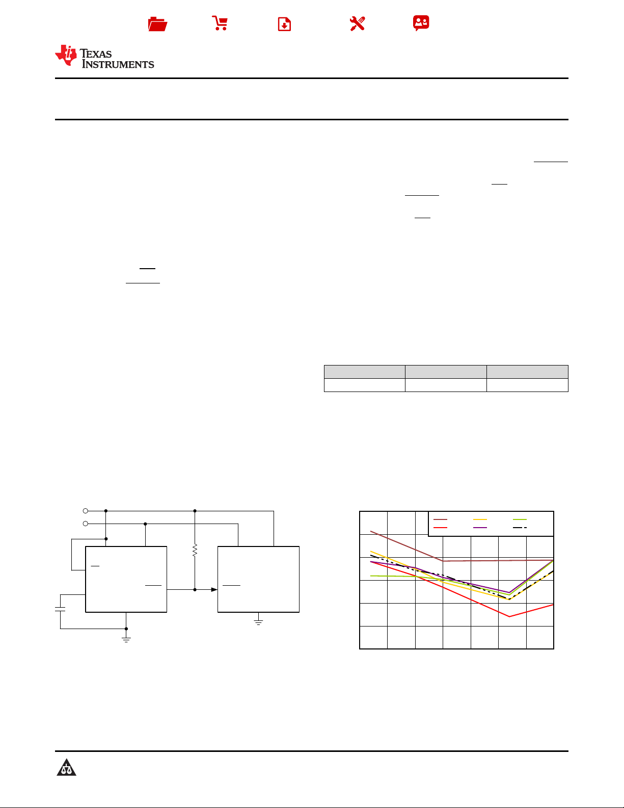
Accuracy vs Temperature
ITN

TPS3890
SLVSD65A –MARCH 2016–REVISED MAY 2016
www.ti.com
Table of Contents
1 Features.................................................................. 1
2 Applications ........................................................... 1
3 Description ............................................................. 1
4 Revision History..................................................... 2
5 Device Comparison Table..................................... 3
6 Pin Configuration and Functions......................... 3
7 Specifications......................................................... 4
7.1 Absolute Maximum Ratings...................................... 4
7.2 ESD Ratings ............................................................ 4
7.3 Recommended Operating Conditions....................... 4
7.4 Thermal Information.................................................. 4
7.5 Electrical Characteristics........................................... 5
7.6 Timing Requirements................................................ 5
7.7 Typical Characteristics.............................................. 7
8 Detailed Description............................................ 11
8.1 Overview................................................................. 11
8.2 Functional Block Diagram....................................... 11
8.3 Feature Description................................................. 11
8.4 Device Functional Modes........................................ 14
9 Application and Implementation ........................ 15
9.1 Application Information............................................ 15
9.2 Typical Application ................................................. 15
10 Power Supply Recommendations ..................... 16
11 Layout................................................................... 17
11.1 Layout Guidelines ................................................. 17
11.2 Layout Example .................................................... 17
12 Device and Documentation Support................. 18
12.1 Documentation Support ....................................... 18
12.2 Community Resources.......................................... 18
12.3 Trademarks........................................................... 18
12.4 Electrostatic Discharge Caution............................ 18
12.5 Glossary................................................................ 18
13 Mechanical, Packaging, and Orderable
Information........................................................... 18
4 Revision History
NOTE: Page numbers for previous revisions may differ from page numbers in the current version.
Changes from Original (March 2016) to Revision A Page
• Released to production........................................................................................................................................................... 1
2
Submit Documentation Feedback Copyright © 2016, Texas Instruments Incorporated
Product Folder Links: TPS3890

1SENSE
2GND
3MR 4 VDD
5 CT
6 RESET
Not to scale
www.ti.com
5 Device Comparison Table
TPS3890
SLVSD65A –MARCH 2016–REVISED MAY 2016
PART NUMBER NOMINAL SUPPLY VOLTAGE NEGATIVE THRESHOLD (V
TPS389001 Adjustable 1.15 V 1.157 V
TPS389012 1.2 V 1.15 V 1.157 V
TPS389015 1.5 V 1.44 V 1.449 V
TPS389018 1.8 V 1.73 V 1.740 V
TPS389020 2.0 V 1.90 V 1.911 V
TPS389025 2.5 V 2.40 V 2.414 V
TPS389030 3.0 V 2.89 V 2.907 V
TPS389033 3.3 V 3.17 V 3.189 V
6 Pin Configuration and Functions
DSE Package
6-Pin WSON
Top View
) POSITIVE THRESHOLD (V
ITN
ITP
)
Pin Functions
PIN
NO. NAME
5 CT —
2 GND — Ground
3 MR I Driving the manual reset pin (MR) low causes RESET to go low (assert).
6 RESET O
1 SENSE I
4 VDD I Supply voltage pin. Good analog design practice is to place a 0.1-µF ceramic capacitor close to this pin.
I/O DESCRIPTION
The CT pin offers a user-adjustable delay time. Connecting this pin to a ground-referenced capacitor sets
the RESET delay time to deassert.
t
(sec) = CCT(µF) × 1.07 + 25 µs (nom).
PD(r)
RESET is an open-drain output that is driven to a low-impedance state when either the MR pin is driven to
a logic low or the monitored voltage on the SENSE pin is lower than the negative threshold voltage (V
RESET remains low (asserted) for the delay time period after both MR is set to a logic high and the
SENSE input is above V
. A pullup resistor from 10 kΩ to 1 MΩ can be used on this pin.
ITP
This pin is connected to the voltage to be monitored. When the voltage on SENSE falls below the
negative threshold voltage V
positive threshold voltage V
, RESET goes low (asserts). When the voltage on SENSE rises above the
ITN
, RESET goes high (deasserts).
ITP
ITN
).
Product Folder Links: TPS3890
Submit Documentation FeedbackCopyright © 2016, Texas Instruments Incorporated
3

TPS3890
SLVSD65A –MARCH 2016–REVISED MAY 2016
www.ti.com
7 Specifications
7.1 Absolute Maximum Ratings
over operating junction temperature range (unless otherwise noted)
VDD –0.3 7
SENSE –0.3 7
Voltage
RESET –0.3 7
MR –0.3 7
V
CT
Current RESET –20 20 mA
Temperature
Operating junction temperature, T
Storage temperature, T
(1) Stresses beyond those listed under Absolute Maximum Ratings may cause permanent damage to the device. These are stress ratings
only, which do not imply functional operation of the device at these or any other conditions beyond those indicated under Recommended
Operating Conditions. Exposure to absolute-maximum-rated conditions for extended periods may affect device reliability.
7.2 ESD Ratings
V
(ESD)
Electrostatic discharge
(1) JEDEC document JEP155 states that 500-V HBM allows safe manufacturing with a standard ESD control process. Manufacturing with
less than 500-V HBM is possible with the necessary precautions.
(2) JEDEC document JEP157 states that 250-V CDM allows safe manufacturing with a standard ESD control process. Manufacturing with
less than 250-V CDM is possible with the necessary precautions.
Human-body model (HBM), per ANSI/ESDA/JEDEC JS-001
Charged-device model (CDM), per JEDEC specification JESD22-C101
(1)
MIN MAX UNIT
V
–0.3 7
J
stg
–40 125
–65 150
°C
VALUE UNIT
(1)
±1000
(2)
±750
V
7.3 Recommended Operating Conditions
over operating free-air temperature range (unless otherwise noted)
MIN NOM MAX UNIT
V
DD
V
SENSE
V
RESET
I
RESET
C
IN
C
CT
R
PU
T
J
Power-supply voltage 1.5 5.5 V
SENSE voltage 0 5.5 V
RESET pin voltage 0 5.5 V
RESET pin current –5 5 mA
Input capacitor, VDD pin 0 0.1 µF
Reset timeout capacitor, CT pin 0 22 µF
Pullup resistor, RESET pin 1 1000 kΩ
Junction temperature (free-air temperature) –40 25 125 ℃
7.4 Thermal Information
TPS3890
THERMAL METRIC
R
θJA
R
θJC(top)
R
θJB
ψ
JT
ψ
JB
R
θJC(bot)
Junction-to-ambient thermal resistance 321.3 °C/W
Junction-to-case (top) thermal resistance 207.9 °C/W
Junction-to-board thermal resistance 281.5 °C/W
Junction-to-top characterization parameter 42.4 °C/W
Junction-to-board characterization parameter 284.8 °C/W
Junction-to-case (bottom) thermal resistance 142.3 °C/W
(1) For more information about traditional and new thermal metrics, see the Semiconductor and IC Package Thermal Metrics application
report, SPRA953.
(1)
UNITDSE (WSON)
6 PINS
4
Submit Documentation Feedback Copyright © 2016, Texas Instruments Incorporated
Product Folder Links: TPS3890

TPS3890
www.ti.com
SLVSD65A –MARCH 2016–REVISED MAY 2016
7.5 Electrical Characteristics
over the operating junction temperature range of –40°C to +125°C, 1.5 V ≤ VDD≤ 5.5 V, and MR = VDD(unless otherwise
noted); typical values are at VDD= 5.5 V and TJ= 25°C
PARAMETER TEST CONDITIONS MIN TYP MAX UNIT
V
DD
V
POR
I
DD
V
ITN
V
HYST
I
SENSE
I
CT
V
CT
R
CT
V
IL
V
IH
V
OL
I
LKG(OD)
(1) V
, V
Input supply voltage 1.5 5.5 V
Power-on reset voltage V
Supply current (into VDD pin)
SENSE input threshold voltage
ITP
accuracy
Hysteresis
(1)
Input current
VDD= 3.3 V, I
–40°C < TJ< 85°C
VDD= 3.3 V, I
–40°C < TJ< 105°C
VDD= 3.3 V, I
VDD= 5.5 V, I
–40°C < TJ< 85°C
VDD= 5.5 V, I
–40°C < TJ< 105°C
VDD= 5.5 V, I
V
V
TPS389012
OL(max)
= 0.2 V, I
RESET
RESET
RESET
RESET
RESET
RESET
= 15 µA 0.8 V
RESET
= 0 mA,
2.09 3.72
= 0 mA,
= 0 mA 5.8
= 0 mA,
2.29 4
= 0 mA,
= 0 mA 6.5
–1% ±0.5% 1%
0.325% 0.575% 0.825%
= 5 V 8 µA
SENSE
= 5 V, TPS389001,
SENSE
10 100 nA
CT pin charge current 0.90 1.15 1.35 µA
CT pin comparator threshold voltage 1.17 1.23 1.29 V
CT pin pulldown resistance When RESET is deasserted 200 Ω
Low-level input voltage (MR pin) 0.25 × V
High-level output voltage 0.7 x V
Low-level output voltage
Open-drain output leakage
= [(V
HYST
ITP
– V
ITN
) / V
] × 100%.
ITN
VDD≥ 1.5 V, I
VDD≥ 4.5 V, I
High impedance,
V
= V
SENSE
RESET
= 0.4 mA 0.25
RESET
= 2 mA 0.25
RESET
= 3 mA 0.3
RESET
= 5.5 V
DD
4.5
5.2
DD
250 nA
µA
V
V
VVDD≥ 2.7 V, I
7.6 Timing Requirements
over the operating junction temperature range of –40°C to +125°C, 1.5 V ≤ VDD≤ 5.5 V, MR = VDD, and 5% input overdrive
(unless otherwise noted); typical values are at VDD= 5.5 V and TJ= 25°C
MIN NOM MAX UNIT
t
PD(f)
t
PD(r)
t
GI(SENSE)
t
GI(MR)
t
MRW
t
d(MR)
t
STRT
SENSE (falling) to RESET propagation delay
SENSE (rising) to RESET propagation delay CT= open, VDD= 3.3 V 25 µs
SENSE pin glitch immunity VDD= 5.5 V 9 µs
MR pin glitch immunity VDD= 5.5 V 100 ns
MR pin pulse duration to assert RESET 1 µs
MR pin low to out delay 250 ns
Startup delay 325 µs
(1) Overdrive = | (VIN/ V
THRESH
– 1) × 100% |.
Product Folder Links: TPS3890
CT= open, VDD= 3.3 V 18
CT= open, VDD= 5.5 V 8
Submit Documentation FeedbackCopyright © 2016, Texas Instruments Incorporated
µs
(1)
5
Time
0.8 V
V
ITP
V
ITN
0.7 V
DD
0.3 V
DD
MR
SENSE
RESET
V
DD
t
PD(r)
t
PD(f)
t
PD(r)
t
PD(r)
=SENSE Rising Propagation Delay
= Undefined State
t
d(MR)
=SENSE Falling Propagation Delay
t
PD(f)
TPS3890
SLVSD65A –MARCH 2016–REVISED MAY 2016
www.ti.com
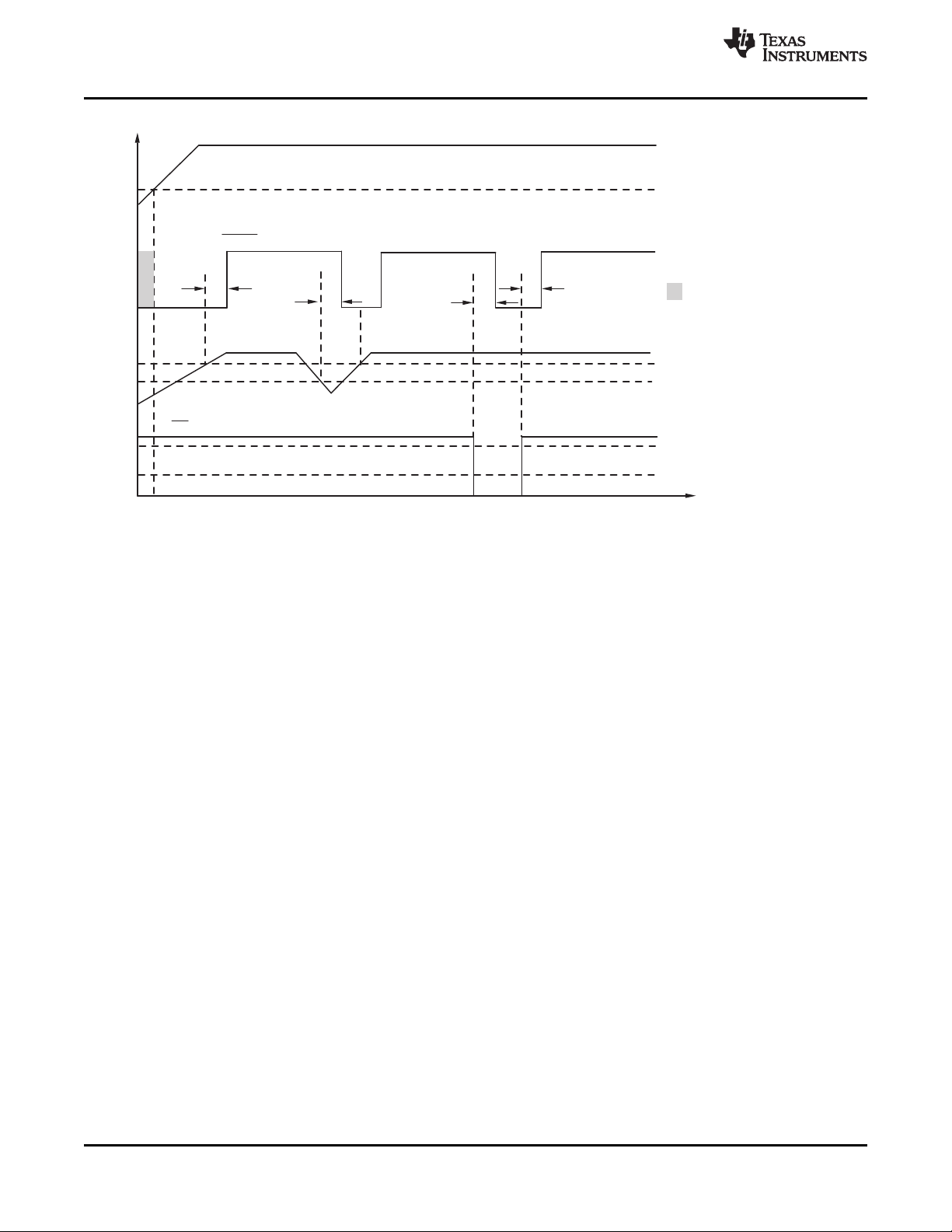
Figure 1. Timing Diagram
6
Submit Documentation Feedback Copyright © 2016, Texas Instruments Incorporated
Product Folder Links: TPS3890
Temperature (qC)
CT Current (PA)
-50 -25 0 25 50 75 100 125
1
1.05
1.1
1.15
1.2
D005
1.5 V
5.5 V
Hysteresis (%)
Frequency (%)
0
3
6
9
12
15
0.47 0.51 0.55 0.59 0.63 0.67
V
ITN
Accuracy (%)
Frequency (%)
0
2
4
6
8
10
12
-0.25 -0.15 -0.05 0.05 0.15 0.25
V
ITP
Accuracy (%)
Frequency (%)
0
2
4
6
8
10
12
-0.25 -0.15 -0.05 0.05 0.15 0.25
Temperature (qC)
Accuracy (%)
-50 -25 0 25 50 75 100 125
-0.75
-0.5
-0.25
0
0.25
0.5
0.75
D001
Unit 1
Unit 2
Unit 3
Unit 4
Unit 5
Avg
Temperature (qC)
Accuracy (%)
-50 -25 0 25 50 75 100 125
-0.75
-0.5
-0.25
0
0.25
0.5
0.75
D002
Unit 1
Unit 2
Unit 3
Unit 4
Unit 5
Avg
TPS3890
www.ti.com
SLVSD65A –MARCH 2016–REVISED MAY 2016
7.7 Typical Characteristics
over the operating junction temperature range of –40°C to +125°C, 1.5 V ≤ VDD≤ 5.5 V, and MR = VDD(unless otherwise
noted)
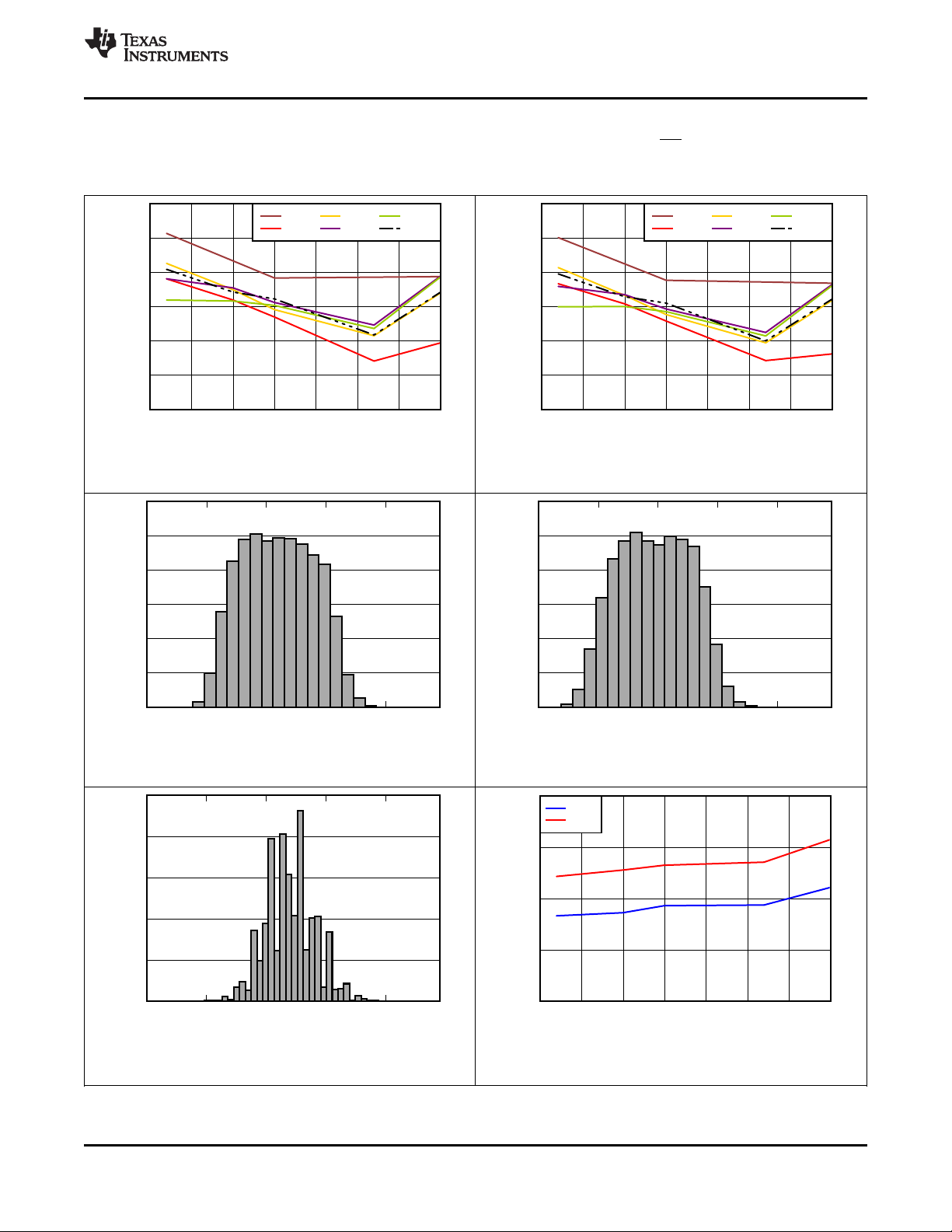
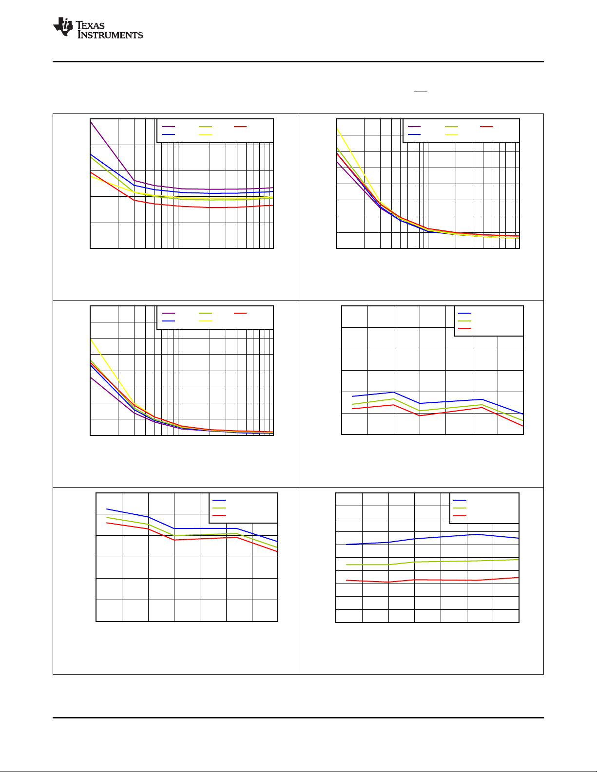
Figure 2. V
Accuracy vs Temperature Figure 3. V
ITN
Tested at VDD= 1.5 V and VDD= 5.5 V, total tests = 136,348
Figure 4. V
Accuracy Histogram
ITN
Accuracy vs Temperature
ITP
Tested at VDD= 1.5 V and VDD= 5.5 V, total tests = 136,348
Figure 5. V
Accuracy Histogram
ITP
Tested at VDD= 1.5 V and VDD= 5.5 V, total tests = 136,348
Figure 6. Hysteresis Histogram
Product Folder Links: TPS3890
Figure 7. CT Current vs Temperature
Submit Documentation FeedbackCopyright © 2016, Texas Instruments Incorporated
7
Temperature (qC)
Startup Delay (Ps)
-50 -25 0 25 50 75 100 125
0
100
200
300
400
500
600
D008
VCC = 1.5 V
VCC = 3.3 V
VCC = 5.5 V
Overdrive (%)
Propagation Delay (Ps)
1 10 100
29
30
31
32
33
34
D009
-40qC
0qC
25qC
85qC
125qC
Temperature (qC)
MR Threshold (V)
-50 -25 0 25 50 75 100 125
0
0.25
0.5
0.75
1
D006
V
IL
V
IH
Temperature (qC)
MR Threshold (V)
-50 -25 0 25 50 75 100 125
1
1.25
1.5
1.75
2
2.25
2.5
2.75
3
V
IL
V
IH
VDD (V)
Supply Current (PA)
0 0.5 1 1.5 2 2.5 3 3.5 4 4.5 5 5.5
0
1
2
3
4
5
6
D004
-40qC
0qC
25qC
85qC
105qC
125qC
VDD (V)
Supply Current (PA)
0 0.5 1 1.5 2 2.5 3 3.5 4 4.5 5 5.5
0
1
2
3
4
5
6
-40qC
0qC
25qC
85qC
105qC
125q
TPS3890
SLVSD65A –MARCH 2016–REVISED MAY 2016
www.ti.com
Typical Characteristics (continued)
over the operating junction temperature range of –40°C to +125°C, 1.5 V ≤ VDD≤ 5.5 V, and MR = VDD(unless otherwise
noted)
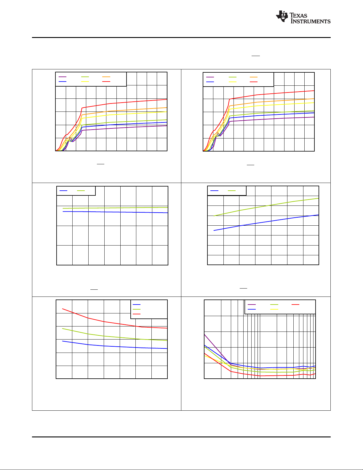
MR = V
DD
Figure 8. Supply Current vs Power-Supply Voltage
Figure 9. Supply Current vs Power-Supply Voltage
MR = 0 V
VDD= 1.5 V
Figure 10. MR Threshold vs Temperature
Figure 12. Startup Delay vs Temperature
8
Submit Documentation Feedback Copyright © 2016, Texas Instruments Incorporated
Figure 13. Propagation Delay (t
Product Folder Links: TPS3890
VDD= 5.5 V
Figure 11. MR Threshold vs Temperature
VDD= 5.5 V
) vs Overdrive
PD(r)
Temperature (qC)
SENSE Glitch Immunity (Ps)
-50 -25 0 25 50 75 100 125
0
2
4
6
8
10
12
14
16
18
20
D017
Overdrive=3%
Overdrive=5%
Overdrive=10%
Temperature (qC)
SENSE Glitch Immunity (Ps)
-50 -25 0 25 50 75 100 125
29
29.5
30
30.5
31
31.5
32
Overdrive=3%
Overdrive=5%
Overdrive=10%
Overdrive (%)
Propagation Delay (Ps)
1 10 100
2
6
10
14
18
22
26
30
34
D012
-40qC
0qC
25qC
85qC
125qC
Temperature (qC)
SENSE Glitch Immunity (Ps)
-50 -25 0 25 50 75 100 125
29
29.5
30
30.5
31
31.5
32
Overdrive=3%
Overdrive=5%
Overdrive=10%
Overdrive (%)
Propagation Delay (Ps)
1 10 100
29
30
31
32
33
34
D010
-40qC
0qC
25qC
85qC
125qC
Overdrive (%)
Propagation Delay (Ps)
1 10 100
2
6
10
14
18
22
26
30
34
D011
-40qC
0qC
25qC
85qC
125qC
TPS3890
www.ti.com
SLVSD65A –MARCH 2016–REVISED MAY 2016
Typical Characteristics (continued)
over the operating junction temperature range of –40°C to +125°C, 1.5 V ≤ VDD≤ 5.5 V, and MR = VDD(unless otherwise
noted)
VDD= 1.5 V
Figure 14. Propagation Delay (t
VDD= 1.5 V
Figure 16. Propagation Delay (t
) vs Overdrive
PD(r)
) vs Overdrive
PD(f)
VDD= 5.5 V
Figure 15. Propagation Delay (t
) vs Overdrive
PD(f)
VDD= 5.5 V
Figure 17. Low-to-High Glitch Immunity vs Temperature
Figure 18. Low-to-High Glitch Immunity vs Temperature
VDD= 1.5 V
Figure 19. High-to-Low Glitch Immunity vs Temperature
Product Folder Links: TPS3890
VDD= 5.5 V
Submit Documentation FeedbackCopyright © 2016, Texas Instruments Incorporated
9
 Loading...