V
MON(1)
RST
TPS386000
SENSE1
SENSE2
SENSE3
SENSE4L
SENSE4H
VREF
GPIO
R
S1H
Microprocessor
DSP
FPGA
GND
CT1
CT2
CT3
CT4
RESET1
RESET2
RESET3
RESET4
WDO
WDI
V
MR
DD
V
V
V
V
DD1
DD2
DD3
DD4
V
V
V
MON(2)
MON(3)
MON(4)
R
S2H
R
S3H
V
V
V
MON(2)
MON(3)
MON(4)
R
S4H
R
S4L
R
S3L
R
S2L
R
S1L
Product
Folder
Order
Now
Technical
Documents
Tools &
Software
Support &
Community
Reference
Design
TPS386000,TPS386040
SBVS105F –SEPTEMBER 2009–REVISED OCTOBER 2018
TPS386000 and TPS386040 Quad Supply Voltage Supervisors
With Adjustable Delay and Watchdog Timer
1 Features
1
• Four Independent Voltage Supervisors
• Channel 1:
– Adjustable Threshold Down to 0.4 V
– Manual Reset (MR) Input
• Channels 2, 3:
– Adjustable Threshold Down to 0.4 V
• Channel 4:
– Adjustable Threshold at Any Positive or
Negative Voltage
– Window Comparator
• Adjustable Delay Time: 1.4 ms to 10 s
• Threshold Accuracy: 0.25% Typical
• Very Low Quiescent Current: 11 μA Typical
• Watchdog Timer With Dedicated Output
• Well-Controlled Output During Power Up
• TPS386000: Open-Drain RESETn and WDO
• TPS386040: Push-Pull RESETn and WDO
• Package: 4-mm × 4-mm, 20-Pin VQFN
2 Applications
• All DSP and Microcontroller Applications
• All FPGA and ASIC Applications
• Telecom and Wireless Infrastructure
• Industrial Equipment
• Analog Sequencing
3 Description
The TPS3860x0 family of supply voltage supervisors
(SVSs) can monitor four power rails that are greater
than 0.4 V and one power rail less than 0.4 V
(including negative voltage) with a 0.25% (typical)
threshold accuracy. Each of the four supervisory
circuits (SVS-n) assert a RESETn or RESETn output
signal when the SENSEm input voltage drops below
the programmed threshold. With external resistors,
the threshold of each SVS-n can be programmed
(where n = 1, 2, 3, 4 and m = 1, 2, 3, 4L, 4H).
Each SVS-n has a programmable delay before
releasing RESETn or RESETn. The delay time can
be set independently for each SVS from 1.4 ms to 10
s through the CTn pin connection. Only SVS-1 has an
active-low manual reset (MR) input; a logic-low input
to MR asserts RESET1 or RESET1.
SVS-4 monitors the threshold window using two
comparators. The extra comparator can be
configured as a fifth SVS to monitor negative voltage
with voltage reference output VREF.
The TPS3860x0 has a very low quiescent current of
11 μA (typical) and is available in a small, 4-mm x 4mm, VQFN-20 package.
Device Information
PART NUMBER PACKAGE BODY SIZE (NOM)
TPS3860x0 VQFN (20) 4.00 mm × 4.00 mm
(1) For all available packages, see the orderable addendum at
the end of the data sheet.
(1)
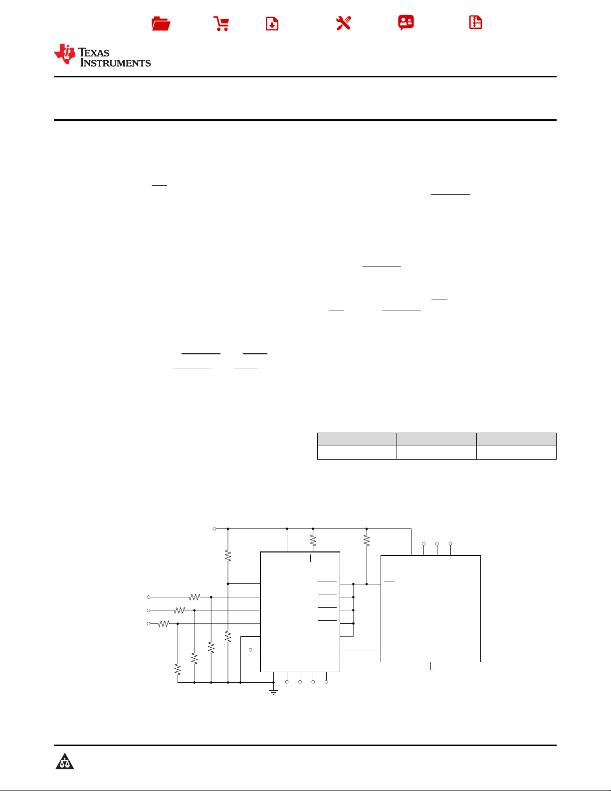
TPS386000 Typical Application Circuit:
Monitoring Supplies for an FPGA
1
An IMPORTANT NOTICE at the end of this data sheet addresses availability, warranty, changes, use in safety-critical applications,
intellectual property matters and other important disclaimers. PRODUCTION DATA.

TPS386000,TPS386040
SBVS105F –SEPTEMBER 2009–REVISED OCTOBER 2018
www.ti.com
Table of Contents
1 Features.................................................................. 1
2 Applications ........................................................... 1
3 Description ............................................................. 1
4 Revision History..................................................... 2
5 Pin Configuration and Functions......................... 4
6 Specifications......................................................... 6
6.1 Absolute Maximum Ratings ..................................... 6
6.2 ESD Ratings.............................................................. 6
6.3 Recommended Operating Conditions....................... 6
6.4 Thermal Information.................................................. 6
6.5 Electrical Characteristics........................................... 7
6.6 Timing Requirements................................................ 8
6.7 Switching Characteristics.......................................... 8
6.8 Typical Characteristics............................................ 14
7 Parameter Measurement Information ................ 18
8 Detailed Description............................................ 19
8.1 Overview ................................................................. 19
8.2 Functional Block Diagrams ..................................... 20
8.3 Feature Description................................................. 22
8.4 Device Functional Modes........................................ 23
9 Application and Implementation ........................ 25
9.1 Application Information............................................ 25
9.2 Typical Application.................................................. 28
10 Power Supply Recommendations ..................... 29
11 Layout................................................................... 30
11.1 Layout Guidelines ................................................. 30
11.2 Layout Example .................................................... 30
12 Device and Documentation Support................. 31
12.1 Device Support .................................................... 31
12.2 Documentation Support ....................................... 31
12.3 Related Links ........................................................ 31
12.4 Community Resources.......................................... 32
12.5 Trademarks........................................................... 32
12.6 Electrostatic Discharge Caution............................ 32
12.7 Glossary................................................................ 32
13 Mechanical, Packaging, and Orderable
Information........................................................... 32
4 Revision History
NOTE: Page numbers for previous revisions may differ from page numbers in the current version.
Changes from Revision E (October 2015) to Revision F Page
• Changed the text in the Power Supply Recommendations section from: This power supply should be less than 1.8 V
in normal operation to: This power supply should not be less than 1.8 V in normal operation............................................ 29
Changes from Revision D (September 2013) to Revision E Page
• Added ESD Ratings table, Feature Description section, Device Functional Modes, Application and Implementation
section, Power Supply Recommendations section, Layout section, Device and Documentation Support section, and
Mechanical, Packaging, and Orderable Information section ................................................................................................. 1
• Changed Features bullets about Channel 1, 2, 3, and 4 ...................................................................................................... 1
• Changed all references of VCC(and ICC) to VDD( and IDD) throughout the document............................................................ 4
• Changed the description of SENSE4L pin function ............................................................................................................... 4
• Changed the description of SENSE4H pin function .............................................................................................................. 4
• Changed the description of MR pin function ......................................................................................................................... 4
• Changed the description of WDI pin function ........................................................................................................................ 4
• Moved ESD ratings from the Absolute Maximum Ratings table to the ESD Ratings table.................................................... 6
• Deleted the Dissipation Ratings table and added the Thermal Information table ................................................................. 6
• Moved timing and switching parameters (tW, tD, t
) from the Electrical Characteristics table to the respective
WDT
Timing Requirements and Switching Characteristics tables .................................................................................................. 8
• Changed the x-axis title notation from CT to CTn in the TPS386040 RESETn Time-out Period vs CTn graph ................. 14
• Changed the Watchdog Timer (WDT) Truth Table; deleted RESET condition column heading ........................................ 24
• Changed title of SENSE INPUT section to Undervoltage Detection ................................................................................... 25
• Changed Equation 1, Equation 2, and Equation 3 VCC notations to V
.......................................................................... 25
MON
• Changed title of Window Comparator section to Undervoltage and Overvoltage Detection ............................................... 25
• Changed VCC4 reference in first paragraph of Undervoltage and Overvoltage Detection section to V
• Changed Equation 4 and Equation 5 VCC4 references to V
....................................................................................... 25
MON(4)
.................... 25
MON(4)
2
Submit Documentation Feedback Copyright © 2009–2018, Texas Instruments Incorporated
Product Folder Links: TPS386000 TPS386040

TPS386000,TPS386040
www.ti.com
• Changed the SVS-4: Window Comparator image ............................................................................................................... 25
• Added VCC to V
in the Window Comparator Operation image................................................................................... 26
MON(4)
• Changed title of Sensing Voltage Less Than 0.4 V to Sensing a Negative Voltage............................................................ 26
• Changed Equation 6 and Equation 7 references to VCC4 to V
MON(4)
• Changed the SVS4: Negative Voltage Sensing image ........................................................................................................ 26
Changes from Revision C (August 2011) to Revision D Page
• Deleted TPS386020 and TPS386060 devices from data sheet............................................................................................. 1
Changes from Revision B (March 2011) to Revision C Page
• Changed Figure 31............................................................................................................................................................... 21
Changes from Revision A (January 2010) to Revision B Page
• Changed data sheet title......................................................................................................................................................... 1
• Changed Features bullets ...................................................................................................................................................... 1
• Changed Applications bullets ................................................................................................................................................. 1
• Changed first sentence of second paragraph in Description text........................................................................................... 1
• Changed low quiescent current value in last paragraph of Description text from 12µA to 11µA........................................... 1
• Changed front-page typical application circuit figure.............................................................................................................. 1
• Added sentence to pin 6 description in Pin Assignments table.............................................................................................. 4
• Changed last sentence of pin 13 description in Pin Assignments table................................................................................. 4
• Added text to first sentence of first paragraph of General Description section.................................................................... 22
• Changed link in Window Comparator section to new Figure 32 .......................................................................................... 25
• Deleted typo in Equation 4 and moved Equation 4 to Window Comparator section............................................................ 25
• Deleted typo in Equation 5 and moved Equation 5 to Window Comparator section............................................................ 25
• Added Figure 32................................................................................................................................................................... 25
• Changed link in Sensing Voltage Less Than 0.4V section to new Figure 34....................................................................... 26
• Added Figure 34................................................................................................................................................................... 26
• Changed caption for Figure 35............................................................................................................................................. 28
SBVS105F –SEPTEMBER 2009–REVISED OCTOBER 2018
................................................................................... 26
Product Folder Links: TPS386000 TPS386040
Submit Documentation FeedbackCopyright © 2009–2018, Texas Instruments Incorporated
3
WDI20
RESET317
RESET2
16
RESET418WDO
19
RESET115
V
DD
14
NC
11
GND12
VREF13
MR
1
CT4
2
CT1
5
CT2 4
CT3 3
6
SENSE29SENSE1
10
SENSE3
8
SENSE4L
7
Thermal Pad
TPS386000,TPS386040
SBVS105F –SEPTEMBER 2009–REVISED OCTOBER 2018
5 Pin Configuration and Functions
www.ti.com
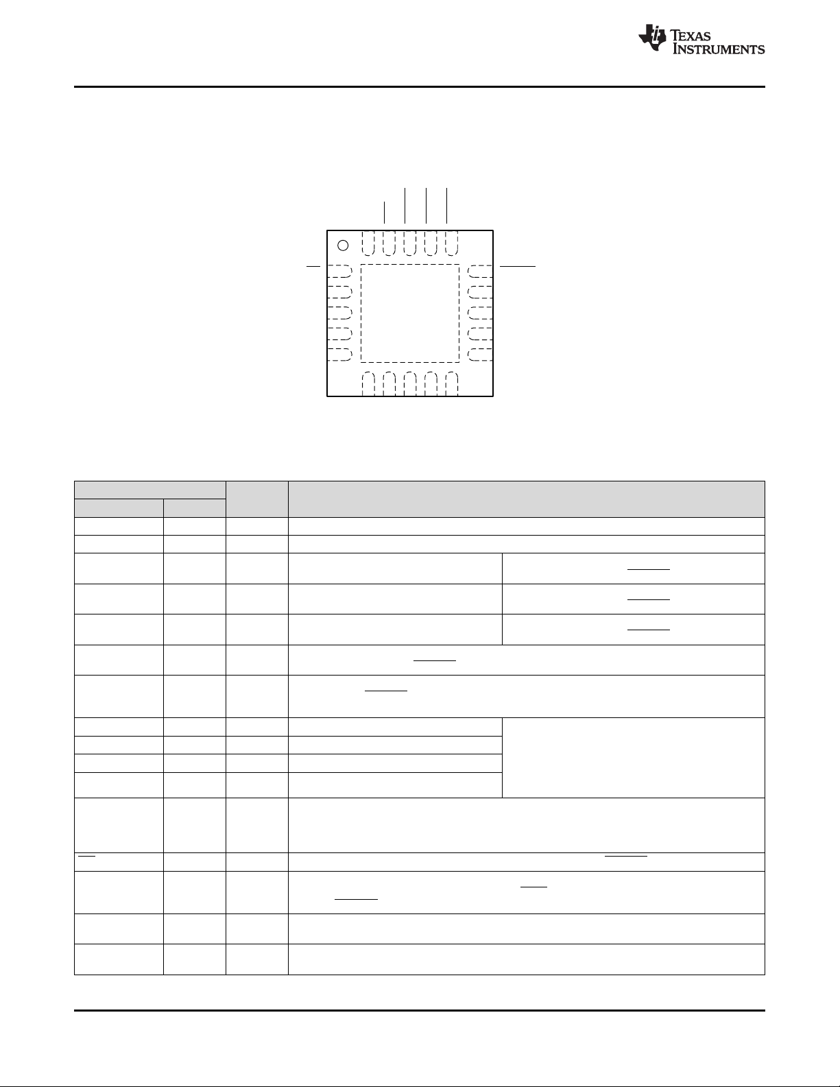
RGP Package
20-Pin VQFN
Top View
Pin Functions
PIN
NAME NO.
V
DD
14 I Supply voltage. TI recommends connecting a 0.1-μF ceramic capacitor close to this pin.
GND 12 — Ground
SENSE1 10 I Monitor voltage input to SVS-1
SENSE2 9 I Monitor voltage input to SVS-2
SENSE3 8 I Monitor voltage input to SVS-3
SENSE4L 7 I
SENSE4H 6 I
CT1 5 — Reset delay programming pin for SVS-1 Connecting this pin to VDDthrough a 40-kΩ to
CT2 4 — Reset delay programming pin for SVS-2
CT3 3 — Reset delay programming pin for SVS-3
CT4 2 — Reset delay programming pin for SVS-4
VREF 13 O
MR 1 I Manual reset input for SVS-1. Logic low level of this pin asserts RESET1.
WDI 20 I
NC 11 —
Thermal Pad PAD —
I/O DESCRIPTION
When the voltage at this terminal drops below the
threshold voltage (V
When the voltage at this terminal drops below the
threshold voltage (V
When the voltage at this terminal drops below the
threshold voltage (V
Falling monitor voltage input to SVS-4. When the voltage at this terminal drops below the
threshold voltage (V
), RESET4 is asserted.
ITN
Rising monitor voltage input to SVS-4. When the voltage at this terminal exceeds the threshold
voltage (V
rail in combination with VREF pin. Connect to GND if not being used.
), RESET4 is asserted. This pin can also be used to monitor the negative voltage
ITP
200-kΩ resistor, or leaving it open, selects a fixed
delay time (see the Electrical Characteristics).
Connecting a capacitor > 220 pF between this pin
and GND selects the programmable delay time (see
the Reset Delay Time section).
Reference voltage output. By connecting a resistor network between this pin and the negative
power rail, SENSE4H can monitor the negative power rail. This pin is intended to only source
current into resistor(s). Do not connect resistor(s) to a voltage higher than 1.2 V. Do not connect
only a capacitor.
Watchdog timer (WDT) trigger input. Inputting either a positive or negative logic edge every
610 ms (typical) prevents WDT time out at the WDO or WDO pin. Timer starts from releasing
event of RESET1.
Not internal connection. TI recommends connecting this pin to the GND pin (pin 12), which is
next to this pin.
This pad is the IC substrate. This pad must be connected only to GND or to the floating thermal
pattern on the printed-circuit board (PCB).
), RESET1 is asserted.
ITN
), RESET2 is asserted.
ITN
), RESET3 is asserted.
ITN
4
Submit Documentation Feedback Copyright © 2009–2018, Texas Instruments Incorporated
Product Folder Links: TPS386000 TPS386040
TPS386000,TPS386040
www.ti.com
SBVS105F –SEPTEMBER 2009–REVISED OCTOBER 2018
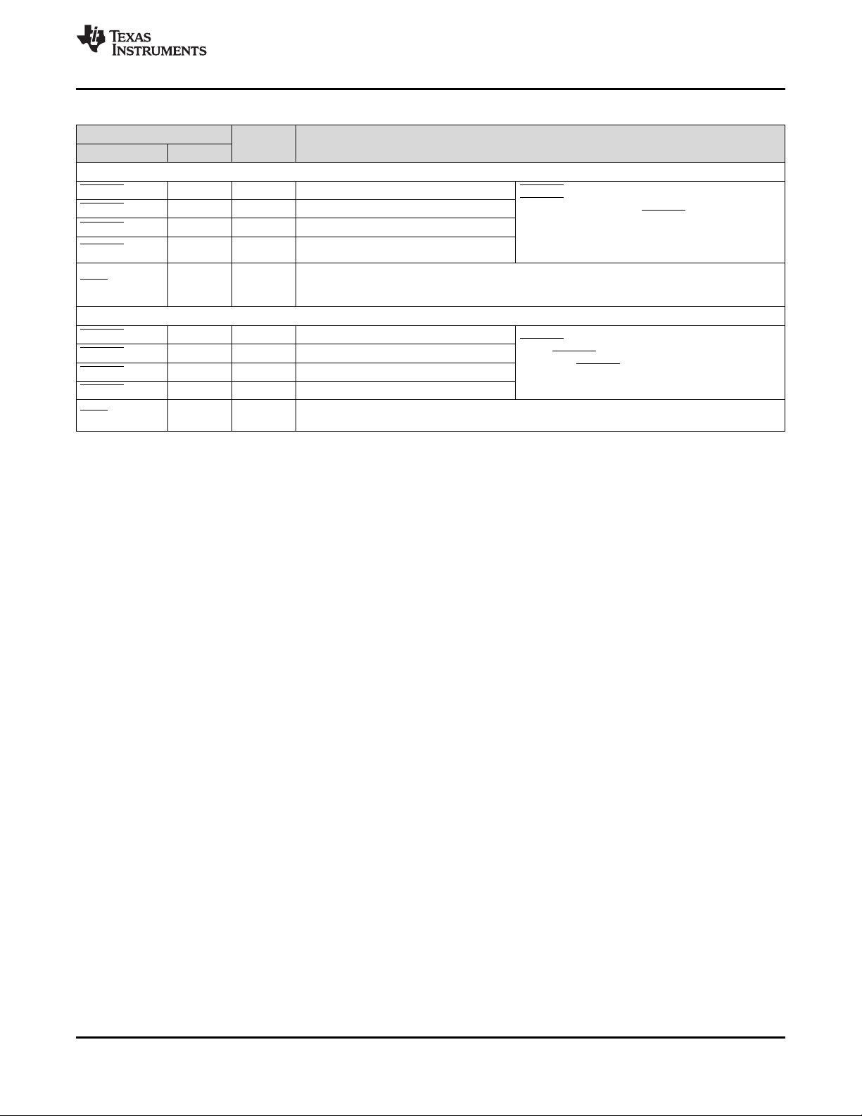
Pin Functions (continued)
PIN
NAME NO.
TPS386000
RESET1 15 O Active low reset output of SVS-1 RESETn is an open-drain output pin. When
RESET2 16 O Active low reset output of SVS-2
RESET3 17 O Active low reset output of SVS-3
RESET4 18 O Active low reset output of SVS-4
WDO 19 O
TPS386040
RESET1 15 O Active low reset output of SVS-1
RESET2 16 O Active low reset output of SVS-2
RESET3 17 O Active low reset output of SVS-3
RESET4 18 O Active low reset output of SVS-4
WDO 19 O
I/O DESCRIPTION
RESETn is asserted, this pin remains in a lowimpedance state. When RESETn is released, this
pin goes to a high-impedance state after the delay
time programmed by CTn. A pullup resistor to V
or another voltage source is required.
Watchdog timer output. This is an open-drain output pin. When WDT times out, this pin goes to
a low-impedance state to GND. If there is no WDT time-out, this pin stays in a high-impedance
state.
RESETn is a push-pull logic buffer output pin.
When RESETn is asserted, this pin remains logic
low. When RESETn is released, this pin goes to
logic high after the delay time programmed by CTn.
Watchdog timer output. This is a push-pull output pin. When WDT times out, this pin goes to
logic low. If there is no WDT time-out, this pin stays in logic high.
DD
Product Folder Links: TPS386000 TPS386040
Submit Documentation FeedbackCopyright © 2009–2018, Texas Instruments Incorporated
5
TPS386000,TPS386040
SBVS105F –SEPTEMBER 2009–REVISED OCTOBER 2018
www.ti.com
6 Specifications
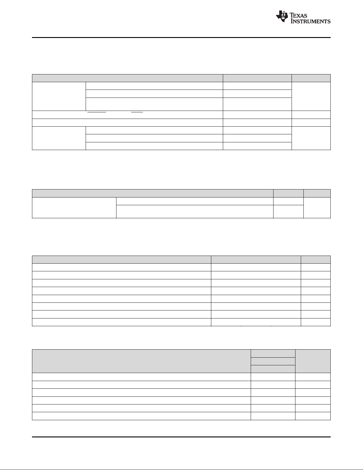
6.1 Absolute Maximum Ratings
SENSE1
(1)
, V
SENSE2
MIN MAX UNIT
–0.3 7
–0.3 VDD+ 0.3
,
–0.3 7
V
–40 150
–40 125
°COperating ambient, T
–65 150
VALUE UNIT
(1)
±2000
±500
V
Over operating junction temperature range, unless otherwise noted.
Input, V
DD
Voltage
CT pin, V
V
RESET1
V
SENSE3
CT1
, V
, V
, V
CT2
RESET2
SENSE4L
, V
, V
, V
, V
CT3
RESET3
SENSE4H
CT4
, V
RESET4
, V
WDI
, VMR, V
, V
WDO
Current RESETn , RESETn, WDO, WDO, VREF pin 5 mA
Power dissipation Continuous total See Thermal Information table
(2)
J
A
Temperature
Operating virtual junction, T
Storage, T
stg
(1) Stresses beyond those listed under Absolute Maximum Ratings may cause permanent damage to the device. These are stress ratings
only, which do not imply functional operation of the device at these or any other conditions beyond those indicated under Recommended
Operating Conditions. Exposure to absolute-maximum-rated conditions for extended periods may affect device reliability.
(2) As a result of the low dissipated power in this device, it is assumed that TJ= TA.
6.2 ESD Ratings
Human-body model (HBM), per ANSI/ESDA/JEDEC JS-001
V
(ESD)
(1) JEDEC document JEP155 states that 500-V HBM allows safe manufacturing with a standard ESD control process.
(2) JEDEC document JEP157 states that 250-V CDM allows safe manufacturing with a standard ESD control process.
Electrostatic discharge
Charged-device model (CDM), per JEDEC specification JESD22-
(2)
C101
6.3 Recommended Operating Conditions
Over operating junction temperature range (unless otherwise noted).
MIN NOM MAX UNIT
V
DD
(1)
V
SENSE
WDI
(HI)
WDI
(LO)
V
MR
CTn 0.22 1000 nF
R
PULL-UP
T
J
(1) All sense inputs.
1.8 6.5 V
0 V
0.7V
DD
0 0.3V
0 V
DD
V
DD
DD
DD
6.5 100 10000 kΩ
–40 25 125 °C
V
V
V
V
6.4 Thermal Information
TPS3860x0
THERMAL METRIC
R
θJA
R
θJC(top)
R
θJB
ψ
JT
ψ
JB
R
θJC(bot)
Junction-to-ambient thermal resistance 46 °C/W
Junction-to-case (top) thermal resistance 52.8 °C/W
Junction-to-board thermal resistance 22.4 °C/W
Junction-to-top characterization parameter 1.3 °C/W
Junction-to-board characterization parameter 22.4 °C/W
Junction-to-case (bottom) thermal resistance 4.3 °C/W
(1) For more information about traditional and new thermal metrics, see the Semiconductor and IC Package Thermal Metrics application
report (SPRA953).
6
Submit Documentation Feedback Copyright © 2009–2018, Texas Instruments Incorporated
Product Folder Links: TPS386000 TPS386040
(1)
UNITRGP (VQFN)
20 PINS
TPS386000,TPS386040
www.ti.com
SBVS105F –SEPTEMBER 2009–REVISED OCTOBER 2018
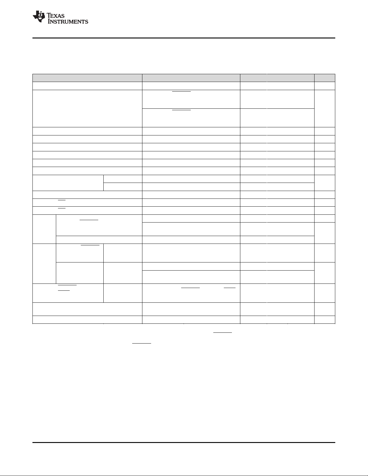
6.5 Electrical Characteristics
Over the operating temperature range of TJ= –40°C to 125°C, 1.8 V < VDD< 6.5 V, R
(TPS386000 only), C
(n = 1, 2, 3, 4L, 4H) = 50 pF to GND, R
RESETn
= 100 kΩ to VDD, C
WDO
to VDD, WDI = GND, and CTn (n = 1, 2, 3, 4) = open, unless otherwise noted. Typical values are at TJ= 25°C.
PARAMETER TEST CONDITIONS MIN TYP MAX UNIT
V
DD
I
DD
V
ITN
V
ITP
V
HYSN
V
HYSP
I
SENSE
I
CT
V
TH(CTn)
V
IL
V
IH
V
OL
V
OH
I
LKG
V
REF
C
IN
(1) Toggling WDI for a period less than t
(2) These specifications are beyond the recommended VDDrange, and only define RESETn or RESETn output performance during V
(3) The lowest supply voltage (VDD) at which RESETn or RESETn becomes active; t
(4) CTn (where n = 1, 2, 3, or 4) are constant current charging sources working from a range of 0 V to V
Input supply range 1.8 6.5 V
Supply current (current into VDDpin)
VDD= 3.3 V, RESETn or RESETn not
asserted, WDI toggling
and VREF open
VDD= 6.5 V, RESETn or RESETn not
asserted, WDI toggling
(1)
, no output load,
(1)
, no output load,
and VREF open
Power-up reset voltage
(2)(3)
VOL(max) = 0.2 V, I
= 15 μA 0.9 V
RESETn
Negative-going input threshold voltage SENSE1, SENSE2, SENSE3, SENSE4L 396 400 404 mV
Positive-going input threshold voltage SENSE4H 396 400 404 mV
Hysteresis (positive-going) on V
ITN
Hysteresis (negative-going) on V
Input current at SENSEm pin V
CTn pin charging
current
CT1 C
CT2, CT3, CT4 C
CTn pin threshold C
SENSE1, SENSE2, SENSE3, SENSE4L 3.5 10 mV
SENSE4H 3.5 10 mV
ITP
= 0.42 V –25 ±1 +25 nA
SENSEm
> 220 pF, V
CT1
> 220 pF, V
CTn
> 220 pF 1.18 1.238 1.299 V
CTn
CT1
CTn
= 0.5 V
= 0.5 V
(4)
(4)
MR and WDI logic low input 0 0.3V
MR and WDI logic high input 0.7V
Low-level RESETn or RESETn output
voltage
IOL= 1 mA 0.4 V
SENSEn = 0 V, 1.3 V < VDD< 1.8 V,
IOL= 0.4 mA
(2)
Low-level WDO output voltage IOL= 1 mA 0.4
High-level RESETn
or RESETn output
voltage
High-level WDO
output voltage
RESETn, RESETn,
WDO, and WDO
leakage current
Reference voltage output
TPS386040
only
TPS386040
only
TPS386000
only
IOL= –1 mA VDD– 0.4 V
IOL= –1 mA VDD– 0.4
SENSEn = 0 V, 1.3 V < VDD< 1.8 V,
IOL= –0.4 mA
V
RESETn
and WDO are logic high
1 μA < I
sink)
(2)
= 6.5 V, RESETn, RESETn, WDO,
< 0.2 mA (source only, no
VREF
Input pin capacitance CTn: 0 V to VDD, other pins: 0 V to 6.5 V 5 pF
negatively affects IDD.
WDT
ramp up.
RISE(VDD)
V
= 0.5 V. For ICTperformance between 0 V and V
CTn
, see Figure 28.
TH(CTn)
(n = 1, 2, 3, 4) = 100 kΩ to V
RESETn
= 50 pF to GND, VMR= 100 kΩ
WDO
11 19
13 22
245 300 355
235 300 365
DD
VDD– 0.3
–300 300 nA
1.18 1.2 1.22 V
≥ 15 μs/V.
, and the device is tested at
TH(CTn)
DD
0.3
DD
μA
nA
V
V
V
V
DD
Product Folder Links: TPS386000 TPS386040
Submit Documentation FeedbackCopyright © 2009–2018, Texas Instruments Incorporated
7
V
DD
SENSE1
V
IT–
t
d
t
d
V
hys–
0.9 V
MR
RESET1
t
t
t
t
TPS386000,TPS386040
SBVS105F –SEPTEMBER 2009–REVISED OCTOBER 2018
6.6 Timing Requirements
Over the operating temperature range of TJ= –40°C to 125°C, 1.8 V < VDD< 6.5 V, R
(TPS386000 only), C
(n = 1, 2, 3, 4L, 4H) = 50 pF to GND, R
RESETn
= 100 kΩ to VDD, C
WDO
to VDD, WDI = GND, and CTn (n = 1, 2, 3, 4) = open, unless otherwise noted. Nominal values are at TJ= 25°C.
MIN TYP MAX UNIT
t
W
Input pulse width to
SENSEm and MR pins
SENSEm: 1.05 V
0.95 V
→ 1.05 V
ITP
MR: 0.7 VDD→ 0.3 V
→ 0.95 V
ITN
ITP
DD
ITN
or
(n = 1, 2, 3, 4) = 100 kΩ to V
RESETn
= 50 pF to GND, VMR= 100 kΩ
WDO
4 μs
1 ns
6.7 Switching Characteristics
Over the operating temperature range of TJ= –40°C to 125°C, 1.8 V < VDD< 6.5 V, R
(TPS386000 only), C
(n = 1, 2, 3, 4L, 4H) = 50 pF to GND, R
RESETn
= 100 kΩ to VDD, C
WDO
to VDD, WDI = GND, and CTn (n = 1, 2, 3, 4) = open, unless otherwise noted. Typical values are at TJ= 25°C.
PARAMETER TEST CONDITIONS MIN TYP MAX UNIT
t
D
t
WDT
RESETn or RESETn
delay time
Watchdog timer time-out period
(1) Start from RESET1 or RESET1 release or last WDI transition.
CTn = Open 14 20 24
CTn = V
(1)
DD
225 300 375
450 600 750 ms
(n = 1, 2, 3, 4) = 100 kΩ to V
RESETn
= 50 pF to GND, VMR= 100 kΩ
WDO
www.ti.com
DD
DD
ms
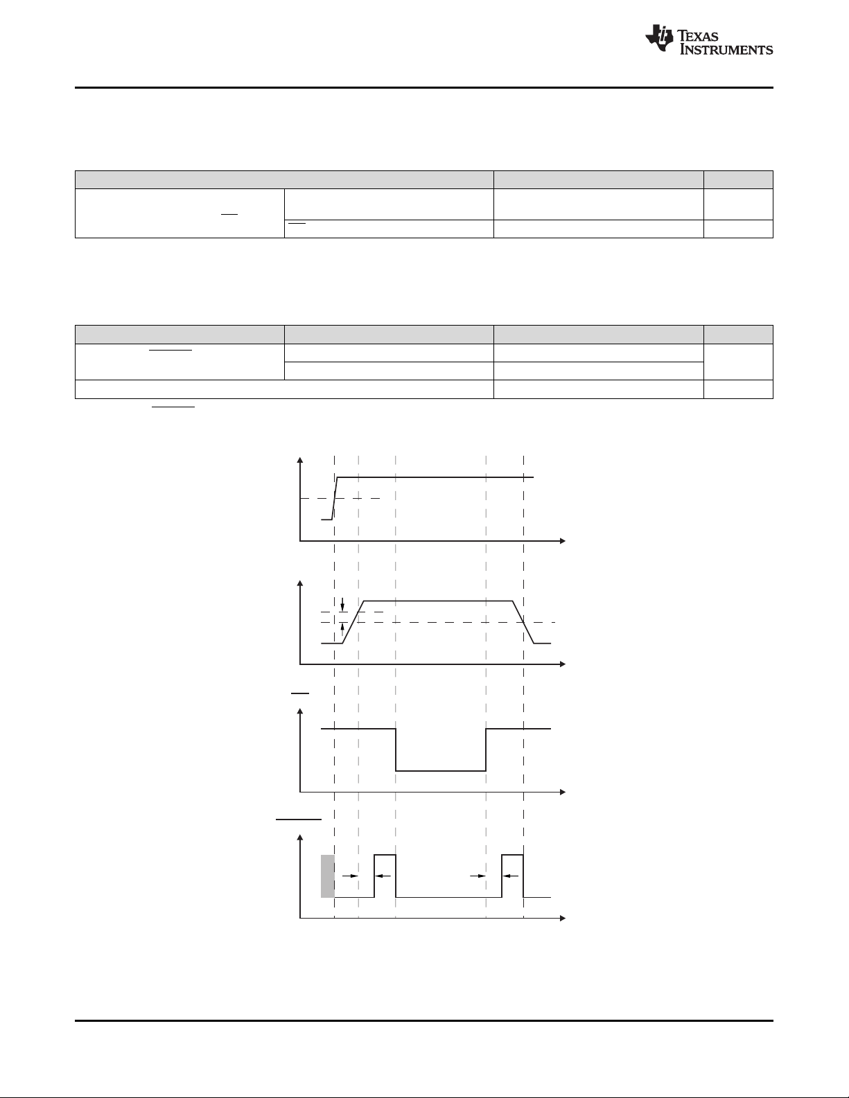
Figure 1. SVS-1 Timing Diagram
8
Submit Documentation Feedback Copyright © 2009–2018, Texas Instruments Incorporated
Product Folder Links: TPS386000 TPS386040
V
DD
SENSE3
V
IT–
V
hys–
0.9 V
RESET3
t
t
t
t
d
t
d
V
CC
SENSE2
V
IT–
V
hys–
0.9 V
RESET2
t
t
t
t
d
www.ti.com
TPS386000,TPS386040
SBVS105F –SEPTEMBER 2009–REVISED OCTOBER 2018
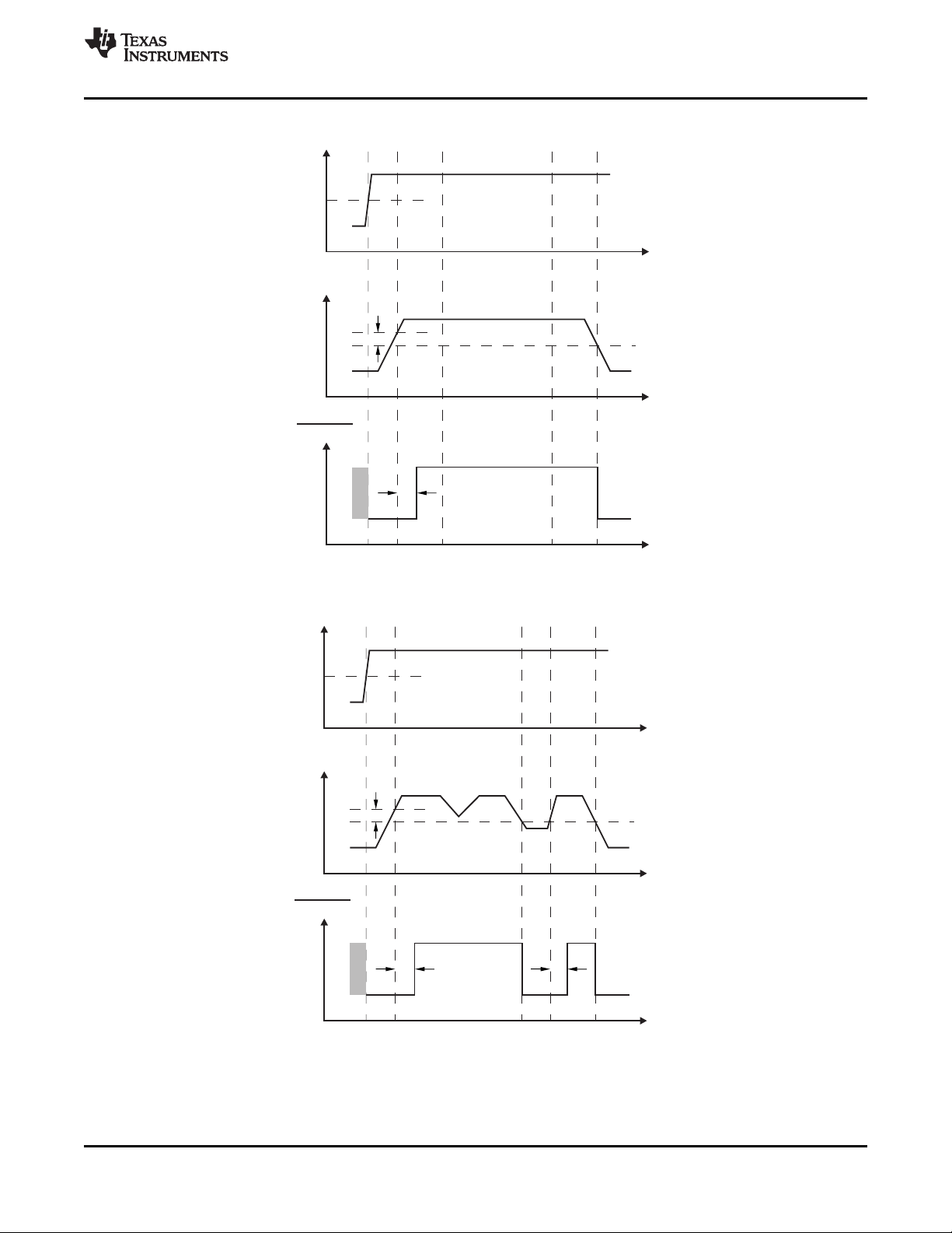
Figure 2. SVS-2 Timing Diagram
Figure 3. SVS-3 Timing Diagram
Submit Documentation FeedbackCopyright © 2009–2018, Texas Instruments Incorporated
Product Folder Links: TPS386000 TPS386040
9
V
DD
SENSE4L
SENSE4H
V
IT–
V
IT+
V
HYS+
V
HYS–
0.9 V
RESET4
t
t
t
t
t
D
TPS386000,TPS386040
SBVS105F –SEPTEMBER 2009–REVISED OCTOBER 2018
www.ti.com
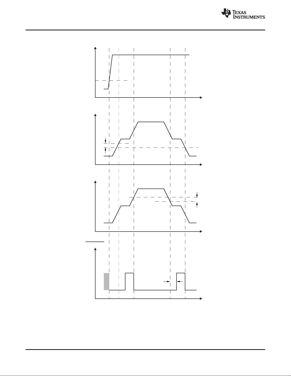
Figure 4. SVS-4 Timing Diagram
10
Submit Documentation Feedback Copyright © 2009–2018, Texas Instruments Incorporated
Product Folder Links: TPS386000 TPS386040
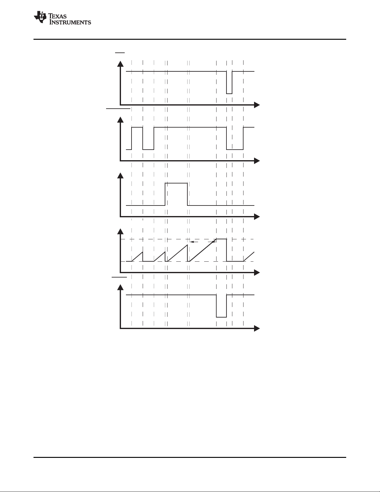
WDI
Zero
Timeout
WDO
RESET1
t
t
t
t
MR
t
t
WDT
(Internaltimer)
www.ti.com
TPS386000,TPS386040
SBVS105F –SEPTEMBER 2009–REVISED OCTOBER 2018
Figure 5. WDT Timing Diagram
Product Folder Links: TPS386000 TPS386040
Submit Documentation FeedbackCopyright © 2009–2018, Texas Instruments Incorporated
11
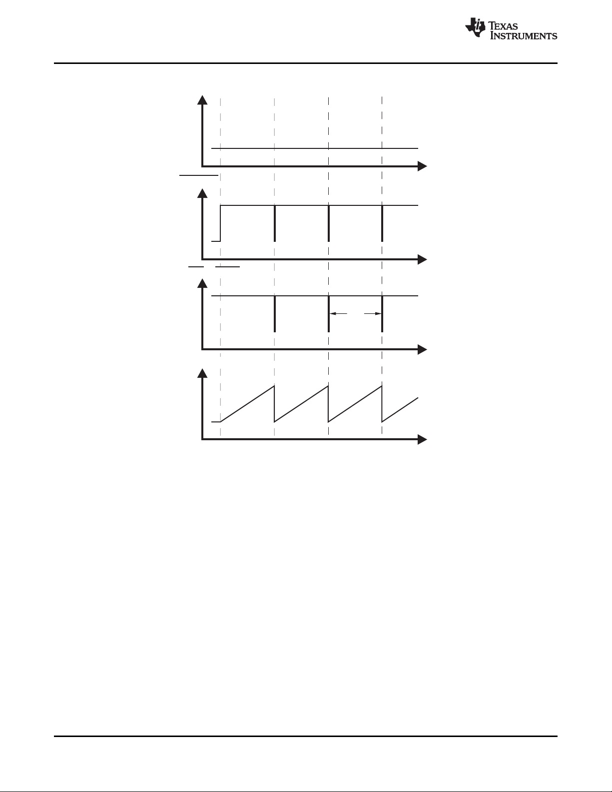
RESET1
t
t
t
(Internaltimer)
MR = WDO
t
WDT
Event1 Event2 Event3
WDI
t
TPS386000,TPS386040
SBVS105F –SEPTEMBER 2009–REVISED OCTOBER 2018
www.ti.com
Figure 6. Legacy WDT Configuration Timing Diagram
12
Submit Documentation Feedback Copyright © 2009–2018, Texas Instruments Incorporated
Product Folder Links: TPS386000 TPS386040
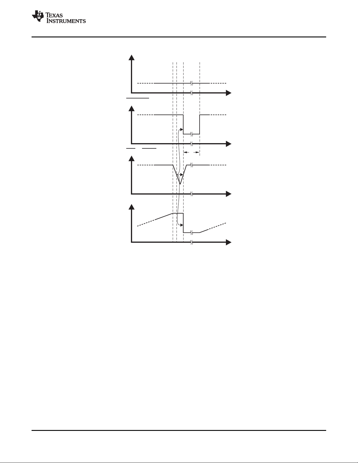
Event1
RESET1
(Internaltimer)
MR = WDO
t
D
WDI
www.ti.com
TPS386000,TPS386040
SBVS105F –SEPTEMBER 2009–REVISED OCTOBER 2018
Figure 7. Enlarged View of Event 1 from Figure 6
Product Folder Links: TPS386000 TPS386040
Submit Documentation FeedbackCopyright © 2009–2018, Texas Instruments Incorporated
13
 Loading...