

Page 1
CHIP FORM
TPS1100, TPS1100Y
SINGLE P-CHANNEL ENHANCEMENT-MODE MOSFETS
SLVS078C – DECEMBER 1993 – REVISED AUGUST 1995
D
Low r
DS(on)
D
3 V Compatible
D
Requires No External V
D
TTL and CMOS Compatible Inputs
D
V
GS(th)
D
Available in Ultrathin TSSOP Package (PW)
D
ESD Protection Up to 2 kV Per
MIL-STD-883C, Method 3015
. . . 0.18 Ω Typ at VGS = –10 V
CC
= –1.5 V Max
description
The TPS1100 is a single P-channel
enhancement-mode MOSFET. The device has
been optimized for 3-V or 5-V power distribution
in battery-powered systems by means of Texas
Instruments LinBiCMOS process. With a
maximum V
0.5 µA, the TPS1100 is the ideal high-side switch
for low-voltage, portable battery-management
systems where maximizing battery life is a primary
concern. The low r
characteristics (rise time 10 ns typical) make the
TPS1100 the logical choice for low-voltage
switching applications such as power switches for
pulse-width-modulated (PWM) controllers or
motor/bridge drivers.
of –1.5 V and an I
GS(th)
DS(on)
and excellent ac
DSS
of only
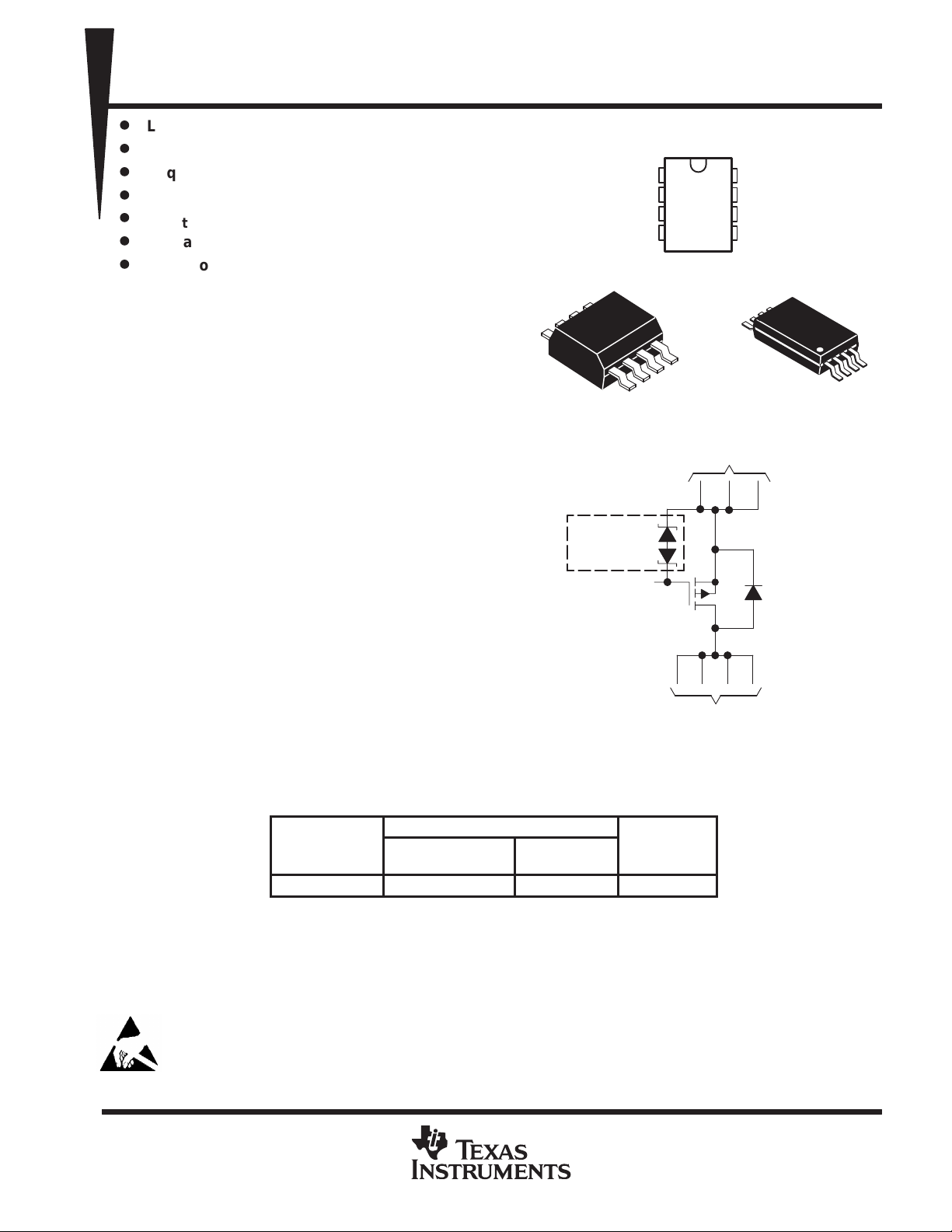
D PACKAGE PW PACKAGE
schematic
SOURCE
SOURCE
SOURCE
GATE
ESD-
Protection
Circuitry
GATE
D OR PW PACKAGE
(TOP VIEW)
1
2
3
4
DRAIN
8
DRAIN
7
DRAIN
6
DRAIN
5
SOURCE
The ultrathin thin shrink small-outline package or
TSSOP (PW) version with its smaller footprint and
reduction in height fits in places where other
P-channel MOSFET s cannot. The size advantage
is especially important where board real estate is
at a premium and height restrictions do not allow
for a small-outline integrated circuit (SOIC)
package.
AVAILABLE OPTIONS
T
A
–40°C to 85°C TPS1100D TPS1100PWLE TPS1100Y
The D package is available taped and reeled. Add an R suffix to device type (e.g.,
TPS1100DR). The PW package is available only left-end taped and reeled
(indicated by the LE suffix on the device type; e.g., TPS1 100PWLE). The chip form
is tested at 25°C.
Caution. This device contains circuits to protect its inputs and outputs against damage due to high static voltages or electrostatic
fields. These circuits have been qualified to protect this device against electrostatic discharges (ESD) of up to 2 kV according to
MIL-STD-883C, Method 3015; however, it is advised that precautions be taken to avoid application of any voltage higher than
maximum-rated voltages to these high-impedance circuits.
LinBiCMOS is a trademark of Texas Instruments Incorporated.
SMALL OUTLINE
NOTE A: For all applications, all source pins should be connected
PACKAGED DEVICES
PLASTIC DIP
(D)
DRAIN
and all drain pins should be connected.
(P)
(Y)
PRODUCTION DATA information is current as of publication date.
Products conform to specifications per the terms of Texas Instruments
standard warranty. Production processing does not necessarily include
testing of all parameters.
POST OFFICE BOX 655303 • DALLAS, TEXAS 75265
Copyright 1995, Texas Instruments Incorporated
1
Page 2
TPS1100, TPS1100Y
SINGLE P-CHANNEL ENHANCEMENT-MODE MOSFETS
SLVS078C – DECEMBER 1993 – REVISED AUGUST 1995
description (continued)
Such applications include notebook computers, personal digital assistants (PDAs), cellular telephones, and
PCMCIA cards. For existing designs, the D-packaged version has a pinout common with other p-channel
MOSFETs in SOIC packages.
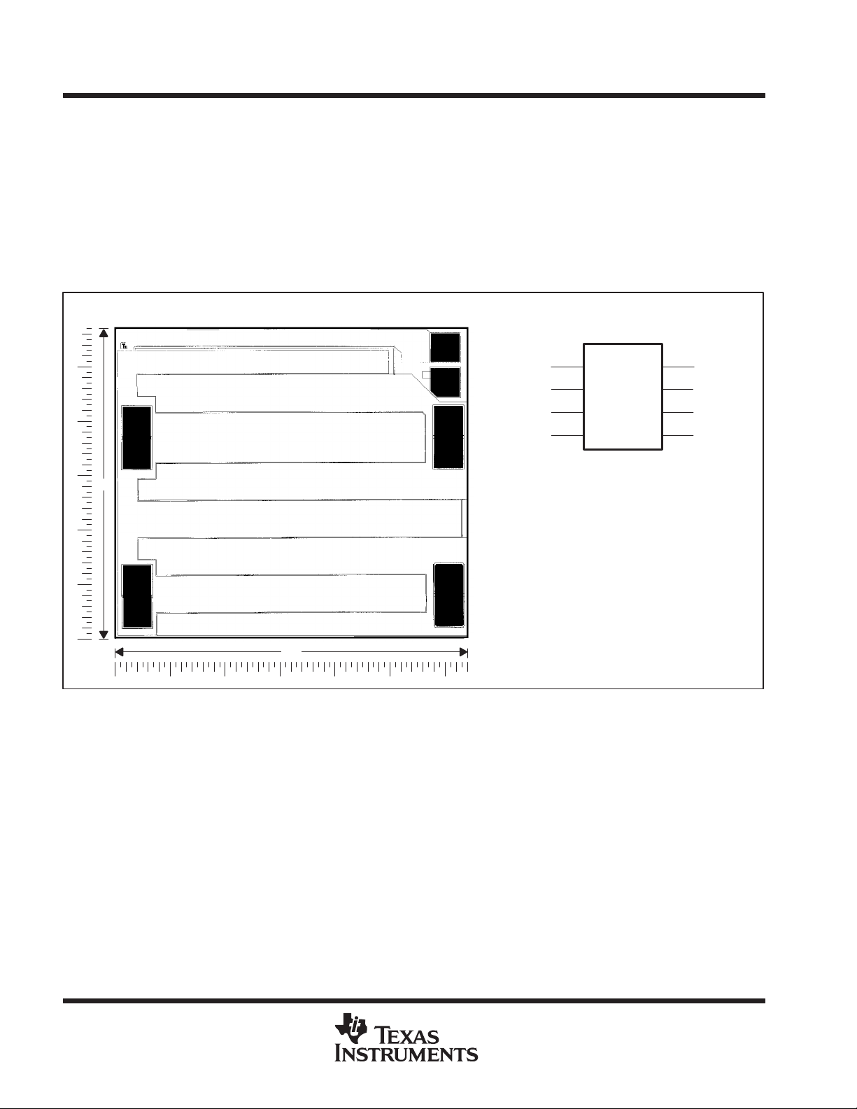
TPS1100Y chip information
This chip, when properly assembled, displays characteristics similar to the TPS1 100. Thermal compression or
ultrasonic bonding may be used on the doped aluminum bonding pads. The chips may be mounted with
conductive epoxy or a gold-silicon preform.
BONDING PAD ASSIGNMENTS
57
(5)
(6)
(8)
(7)
64
(4)
(3)
(1)
(2)
(1)
SOURCE
SOURCE
(2)
(3)
GATE
CHIP THICKNESS: 15 MILS TYPICAL
BONDING PADS: 4 × 4 MILS MINIMUM
TJmax = 150°C
TOLERANCES ARE ±10%
ALL DIMENSIONS ARE IN MILS
TPS1100Y
(8)
(7)
(6)
(5)(4)
DRAINSOURCE
DRAIN
DRAIN
DRAIN
2
POST OFFICE BOX 655303 • DALLAS, TEXAS 75265
Page 3
D package
V
2.7 V
PW package
D package
V
V
PW package
Continuous drain current (T
150°C), I
‡
A
D package
V
V
PW package
D package
V
10 V
PW package
TPS1100, TPS1100Y
SINGLE P-CHANNEL ENHANCEMENT-MODE MOSFETS
SLVS078C – DECEMBER 1993 – REVISED AUGUST 1995
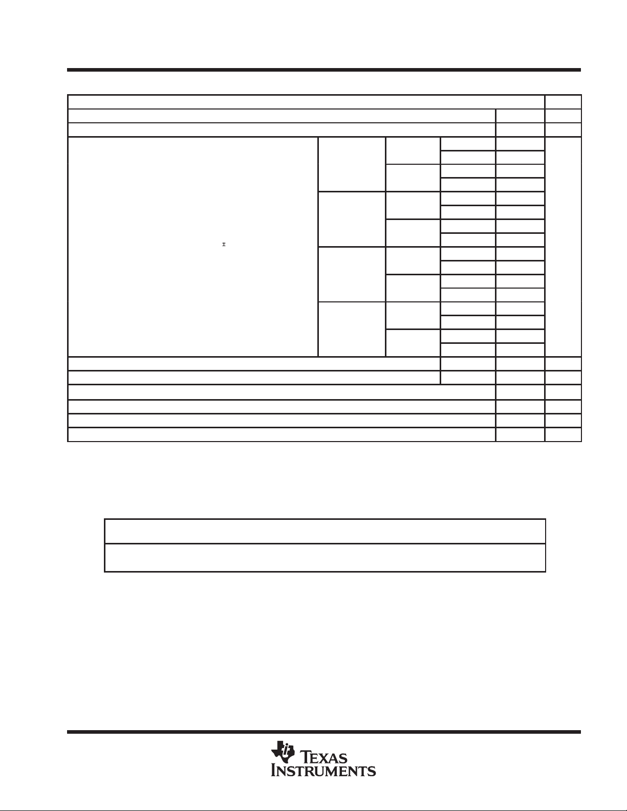
absolute maximum ratings over operating free-air temperature (unless otherwise noted)
Drain-to-source voltage, V
Gate-to-source voltage, V
Pulsed drain current, I
Continuous source current (diode conduction), I
Storage temperature range, T
Operating junction temperature range, T
Operating free-air temperature range, T
Lead temperature 1,6 mm (1/16 inch) from case for 10 seconds 260 °C
†
Stresses beyond those listed under “absolute maximum ratings” may cause permanent damage to the device. These are stress ratings only, and
functional operation of the device at these or any other conditions beyond those indicated under “recommended operating conditions” is not
implied. Exposure to absolute-maximum-rated conditions for extended periods may affect device reliability.
‡
Maximum values are calculated using a derating factor based on R
These devices are mounted on a FR4 board with no special thermal considerations.
DS
GS
p
= –
GS
p
p
= –3
GS
p
°
=
J
‡
D
stg
D
p
= –4.5
GS
p
p
= –
GS
p
S
J
A
= 158°C/W for the D package and R
θJA
TA = 25°C ±0.41
TA = 125°C ±0.28
TA = 25°C ±0.4
TA = 125°C ±0.23
TA = 25°C ±0.6
TA = 125°C ±0.33
TA = 25°C ±0.53
TA = 125°C ±0.27
TA = 25°C ±1
TA = 125°C ±0.47
TA = 25°C ±0.81
TA = 125°C ±0.37
TA = 25°C ±1.6
TA = 125°C ±0.72
TA = 25°C ±1.27
TA = 125°C ±0.58
TA = 25°C ±7 A
TA = 25°C –1 A
= 248°C/W for the PW package.
θJA
2 or –15 V
–55 to 150 °C
–40 to 150 °C
–40 to 125 °C
†
UNIT
–15 V
DISSIPATION RATING TABLE
PACKAGE
D 791 mW 6.33 mW/°C 506 mW 411 mW 158 mW
PW 504 mW 4.03 mW/°C 323 mW 262 mW 101 mW
‡
Maximum values are calculated using a derating factor based on R
for the PW package. These devices are mounted on an FR4 board with no special thermal considerations when tested.
TA ≤ 25°C
POWER RATING
DERATING FACTOR
ABOVE TA = 25°C
POST OFFICE BOX 655303 • DALLAS, TEXAS 75265
‡
TA = 70°C
POWER RATING
θJA
TA = 85°C
POWER RATING
= 158°C/W for the D package and R
POWER RATING
TA = 125°C
= 248°C/W
θJA
3
Page 4
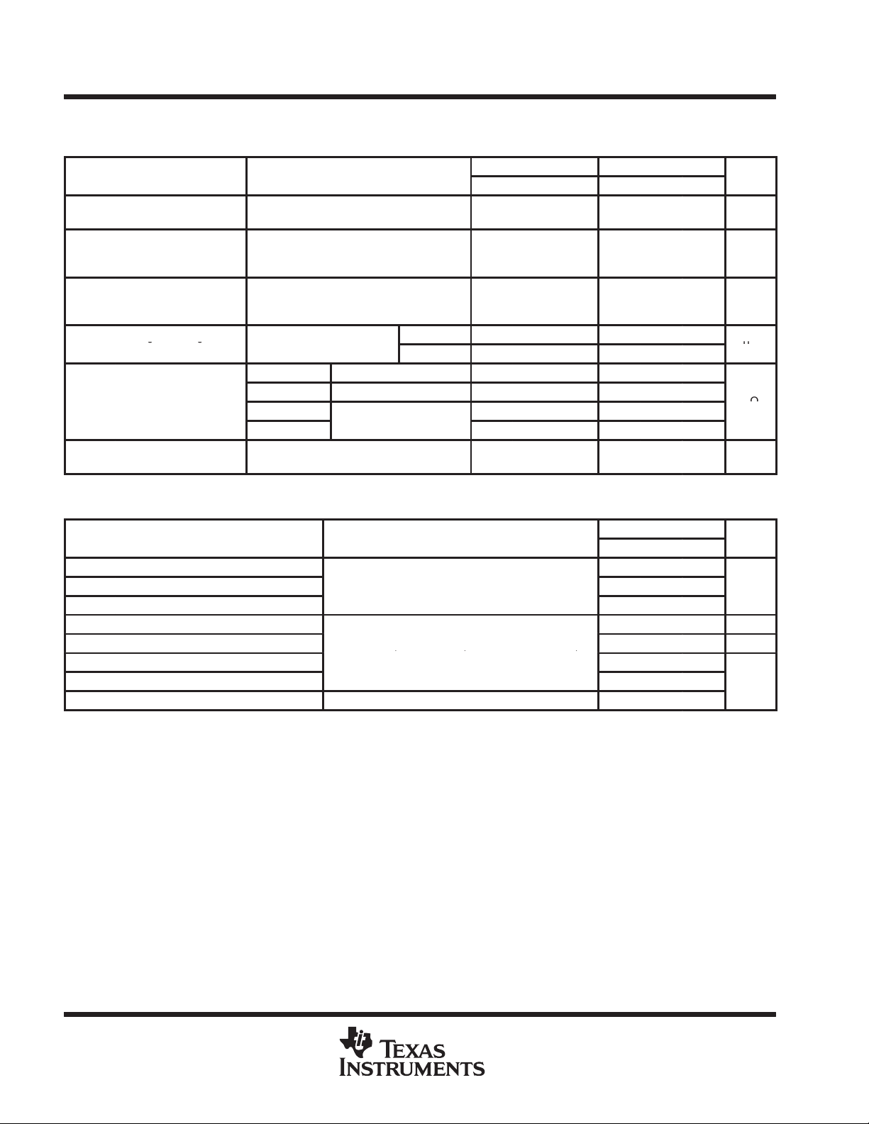
TPS1100, TPS1100Y
PARAMETER
TEST CONDITIONS
UNIT
I
gg
V
V
V
A
r
mΩ
I
A
PARAMETER
TEST CONDITIONS
UNIT
DD
,
L
,
D
,
SINGLE P-CHANNEL ENHANCEMENT-MODE MOSFETS
SLVS078C – DECEMBER 1993 – REVISED AUGUST 1995
electrical characteristics at TJ = 25°C (unless otherwise noted)
static
TPS1100 TPS1100Y
MIN TYP MAX MIN TYP MAX
V
GS(th)
V
SD
I
GSS
DSS
DS(on)
g
fs
†
Pulse test: pulse duration ≤ 300 µs, duty cycle ≤ 2%
Gate-to-source
threshold voltage
Source-to-drain voltage
(diode-forward
†
voltage)
Reverse gate current,
drain short circuited to
source
Zero-gate-voltage drain
current
Static drain-to-source
on-state resistance
Forward
transconductance
†
†
VDS = VGS, ID = –250 µA –1 –1.25 –1.50 –1.25 V
IS = –1 A, VGS = 0 V –0.9 –0.9 V
VDS = 0 V, VGS = –12 V ±100 nA
= –12 V,
DS
VGS = –10 V ID = –1.5 A 180 180
VGS = –4.5 V
VGS = –3 V
VGS = –2.7 V
VDS = –10 V, ID = –2 A 2.5 2.5 S
= 0
GS
ID = –0.5 A 291 400 291
= –0.2
D
TJ = 25°C –0.5
TJ = 125°C –10
µ
476 700 476
606 850 606
dynamic
Q
g
Q
gs
Q
gd
t
d(on)
t
d(off)
t
r
t
f
t
rr(SD)
TPS1100, TPS1100Y
MIN TYP MAX
Total gate charge 5.45
Gate-to-source charge
Gate-to-drain charge 1.4
Turn-on delay time 4.5 ns
Turn-off delay time
Rise time
Fall time 2
Source-to-drain reverse recovery time IF = 5.3 A, di/dt = 100 A/µs 16
VDS = –10 V, VGS = –10 V, ID = –1 A
V
= –10 V, R
RG = 6 Ω,
= 10 Ω,I
See Figures 1 and 2
= –1 A,
0.87
13 ns
10
nC
ns
4
POST OFFICE BOX 655303 • DALLAS, TEXAS 75265
Page 5

TPS1100, TPS1100Y
SINGLE P-CHANNEL ENHANCEMENT-MODE MOSFETS
SLVS078C – DECEMBER 1993 – REVISED AUGUST 1995
PARAMETER MEASUREMENT INFORMATION
R
L
V
V
GS
R
G
DUT
DS
–
V
DD
+
Figure 1. Switching-Time Test Circuit
Drain current vs Drain-to-source voltage 3
Drain current vs Gate-to-source voltage 4
Static drain-to-source on-state resistance vs Drain current 5
Capacitance vs Drain-to-source voltage 6
Static drain-to-source on-state resistance (normalized) vs Junction temperature 7
Source-to-drain diode current vs Source-to-drain voltage 8
Static drain-to-source on-state resistance vs Gate-to-source voltage 9
Gate-to-source threshold voltage vs Junction temperature 10
Gate-to-source voltage vs Gate charge 11
V
GS
90%
10%
V
DS
t
d(on)
t
r
t
d(off)
Figure 2. Switching-Time Waveforms
TYPICAL CHARACTERISTICS
Table of Graphs
0 V
–10 V
t
f
FIGURE
POST OFFICE BOX 655303 • DALLAS, TEXAS 75265
5
Page 6

TPS1100, TPS1100Y
SINGLE P-CHANNEL ENHANCEMENT-MODE MOSFETS
SLVS078C – DECEMBER 1993 – REVISED AUGUST 1995
TYPICAL CHARACTERISTICS
DRAIN CURRENT
vs
DRAIN-TO-SOURCE VOLTAGE
– 7
– 6
– 5
– 4
– 3
– Drain Current – A
D
I
– 2
– 1
0
0 – 1– 2– 3– 4– 5– 6
VGS = –8 V
VGS = –7 V
VGS = –6 V
VGS = –5 V
VDS – Drain-to-Source Voltage – V
VGS = –4 V
VGS = –3 V
VGS = –2 V
TJ = 25°C
– 7 – 8 – 9 – 10
Figure 3 Figure 4
STATIC DRAIN-TO-SOURCE ON-STATE RESISTANCE
vs
DRAIN CURRENT
0.7
TJ = 25°C
0.6
ΩOn-State Resistance –
VGS = –2.7 V
0.5
DRAIN CURRENT
GATE-TO-SOURCE VOLTAGE
– 7
VDS = –10 V
– 6
TJ = 25°C
– 5
TJ = –40°C
– 4
– 3
– Drain Current – A
D
I
– 2
– 1
0
0 – 2 – 3 – 5
VGS – Gate-to-Source Voltage – V
CAPACITANCE
DRAIN-TO-SOURCE VOLTAGE
350
300
250
vs
vs
TJ = 150°C
VGS = 0
f = 1 MHz
TJ = 25°C
C
iss
– 7– 1 – 4 – 6
†
VGS = –3 V
0.4
VGS = –4.5 V
0.3
– Static Drain-to-Source
DS(on)
r
6
VGS = –10 V
0.2
0.1
0
– 0.1 – 1
ID – Drain Current – A
Figure 5
POST OFFICE BOX 655303 • DALLAS, TEXAS 75265
– 10
200
150
C – Capacitance – pF
100
50
0
0 – 1 – 2 – 3 – 4 – 5 – 6
†
C
iss
‡
C
rss
VDS – Drain-to-Source Voltage – V
+
Cgs)
Cgd,C
+
Cgd,C
oss
ds(shorted)
+
Cds)
Figure 6
C
oss
‡
C
rss
– 7 – 8 – 9 –12
CgsC
Cgs)
gd
C
–10 –11
≈ Cds)
gd
C
gd
Page 7

TPS1100, TPS1100Y
SINGLE P-CHANNEL ENHANCEMENT-MODE MOSFETS
SLVS078C – DECEMBER 1993 – REVISED AUGUST 1995
TYPICAL CHARACTERISTICS
STATIC DRAIN-TO-SOURCE
ON-STATE RESISTANCE (NORMALIZED)
vs
JUNCTION TEMPERATURE
1.5
VGS = –10 V
ID = –1A
1.4
1.3
1.2
1.1
1
– Static Drain-to-Source
0.9
0.8
DS(on)
On-State Resistance (normalized)
r
0.7
0.6
–50 0 50 100 150
TJ – Junction Temperature – °C
Figure 7
SOURCE-TO-DRAIN DIODE CURRENT
vs
SOURCE-TO-DRAIN VOLTAGE
–10
Pulse Test
TJ = 150°C
–1
– Source-to-Drain Diode Current – A
SD
I
– 0.1
0 – 0.6 –1.2 –1.8
– 0.2 – 0.4 – 0.8 – 1 –1.4 –1.6
VSD – Source-to-Drain Voltage – V
TJ = 25°C
TJ = –40°C
Figure 8
STATIC DRAIN-TO-SOURCE ON-STATE RESISTANCE
vs
GATE-TO-SOURCE VOLTAGE
0.7
ID = –1 A
0.6
0.5
Ω
0.4
0.3
Resistance –
0.2
– Static Drain-to-Source On-State
0.1
DS(on)
r
0
– 1 – 3 – 5 – 7
VGS – Gate-to-Source Voltage – V
– 9 – 11
TJ = 25°C
– 13 – 15
Figure 9
GATE-TO-SOURCE THRESHOLD VOLTAGE
vs
JUNCTION TEMPERATURE
– 1.5
ID = –250 µA
– 1.4
– 1.3
– 1.2
– 1.1
– Gate-to-Source Threshold Voltage – V
– 1
GS(th)
V
– 0.9
–50 0 50 100 150
TJ – Junction Temperature – °C
Figure 10
POST OFFICE BOX 655303 • DALLAS, TEXAS 75265
7
Page 8

TPS1100, TPS1100Y
SINGLE P-CHANNEL ENHANCEMENT-MODE MOSFETS
SLVS078C – DECEMBER 1993 – REVISED AUGUST 1995
TYPICAL CHARACTERISTICS
GATE-TO-SOURCE VOLTAGE
vs
GATE CHARGE
– 10
VDS = –10 V
ID = –1 A
TJ = 25°C
– 8
– 6
– 4
– Gate-to-Source Voltage – V
GS
– 2
V
0
146
0235
Qg – Gate Charge – nC
Figure 11
8
POST OFFICE BOX 655303 • DALLAS, TEXAS 75265
Page 9

TPS1100, TPS1100Y
SINGLE P-CHANNEL ENHANCEMENT-MODE MOSFETS
SLVS078C – DECEMBER 1993 – REVISED AUGUST 1995
THERMAL INFORMATION
TRANSIENT JUNCTION-TO-AMBIENT
THERMAL IMPEDANCE
vs
PULSE DURATION
Single Pulse
See Note A
– 10
– 1
DRAIN CURRENT
vs
DRAIN-TO-SOURCE VOLTAGE
Single Pulse
See Note A
0.001 s
0.01 s
0.1 s
1 s
C/W
°
100
10
– 0.1
– Drain Current – A
D
I
TJ = 150°C
TA = 25°C
– 0.001
– 0.1 – 1 – 10 – 100
VDS – Drain-to-Source Voltage – V
10 s
DC
Figure 12
NOTE A: Values are for the D package and are FR4-board mounted only.
APPLICATION INFORMATION
3 V or 5 V
Microcontroller
1
Thermal Impedance –
– Transient Junction-to-AmbientZ
θJA
0.1
0.001 0.01 0.1 1 10
tw – Pulse Duration – s
Figure 13
5 V
Driver
Load
Figure 14. Notebook Load Management
POST OFFICE BOX 655303 • DALLAS, TEXAS 75265
Microcontroller
Figure 15. Cellular Phone Output Drive
Charge
Pump
–4 V
GaAs FET
Amplifier
9
Page 10

PACKAGE OPTION ADDENDUM
www.ti.com
8-Aug-2005
PACKAGING INFORMATION
Orderable Device Status
(1)
Package
Type
Package
Drawing
Pins Package
Qty
Eco Plan
TPS1100D ACTIVE SOIC D 8 75 Green (RoHS &
no Sb/Br)
TPS1100DR ACTIVE SOIC D 8 2500 Green (RoHS &
no Sb/Br)
TPS1100DRG4 ACTIVE SOIC D 8 2500 Green (RoHS &
no Sb/Br)
TPS1100PW ACTIVE TSSOP PW 8 150 Green (RoHS &
no Sb/Br)
TPS1100PWLE OBSOLETE TSSOP PW 8 TBD Call TI Call TI
TPS1100PWR ACTIVE TSSOP PW 8 2000 Green (RoHS &
no Sb/Br)
TPS1100PWRG4 ACTIVE TSSOP PW 8 2000 Green (RoHS &
no Sb/Br)
(1)
The marketing status values are defined as follows:
ACTIVE: Product device recommended for new designs.
LIFEBUY: TI has announced that the device will be discontinued, and a lifetime-buy period is in effect.
NRND: Not recommended for new designs. Device is in production to support existing customers, but TI does not recommend using this part in
a new design.
PREVIEW: Device has been announced but is not in production. Samples may or may not be available.
OBSOLETE: TI has discontinued the production of the device.
(2)
Lead/Ball Finish MSL Peak Temp
CU NIPDAU Level-1-260C-UNLIM
CU NIPDAU Level-1-260C-UNLIM
CU NIPDAU Level-1-260C-UNLIM
CU NIPDAU Level-1-260C-UNLIM
CU NIPDAU Level-1-260C-UNLIM
CU NIPDAU Level-1-260C-UNLIM
(3)
(2)
Eco Plan - The planned eco-friendly classification: Pb-Free (RoHS) or Green (RoHS & no Sb/Br) - please check
http://www.ti.com/productcontent for the latest availability information and additional product content details.
TBD: The Pb-Free/Green conversion plan has not been defined.
Pb-Free (RoHS): TI's terms "Lead-Free" or "Pb-Free" mean semiconductor products that are compatible with the current RoHS requirements
for all 6 substances, including the requirement that lead not exceed 0.1% by weight in homogeneous materials. Where designed to be soldered
at high temperatures, TI Pb-Free products are suitable for use in specified lead-free processes.
Green (RoHS & no Sb/Br): TI defines "Green" to mean Pb-Free (RoHS compatible), and free of Bromine (Br) and Antimony (Sb) based flame
retardants (Br or Sb do not exceed 0.1% by weight in homogeneous material)
(3)
MSL, Peak Temp. -- The Moisture Sensitivity Level rating according to the JEDEC industry standard classifications, and peak solder
temperature.
Important Information and Disclaimer:The information provided on this page represents TI's knowledge and belief as of the date that it is
provided. TI bases its knowledge and belief on information provided by third parties, and makes no representation or warranty as to the
accuracy of such information. Efforts are underway to better integrate information from third parties. TI has taken and continues to take
reasonable steps to provide representative and accurate information but may not have conducted destructive testing or chemical analysis on
incoming materials and chemicals. TI and TI suppliers consider certain information to be proprietary, and thus CAS numbers and other limited
information may not be available for release.
In no event shall TI's liability arising out of such information exceed the total purchase price of the TI part(s) at issue in this document sold by TI
to Customer on an annual basis.
Addendum-Page 1
Page 11

IMPORTANT NOTICE
Texas Instruments Incorporated and its subsidiaries (TI) reserve the right to make corrections, modifications,
enhancements, improvements, and other changes to its products and services at any time and to discontinue
any product or service without notice. Customers should obtain the latest relevant information before placing
orders and should verify that such information is current and complete. All products are sold subject to TI’s terms
and conditions of sale supplied at the time of order acknowledgment.
TI warrants performance of its hardware products to the specifications applicable at the time of sale in
accordance with TI’s standard warranty. Testing and other quality control techniques are used to the extent TI
deems necessary to support this warranty . Except where mandated by government requirements, testing of all
parameters of each product is not necessarily performed.
TI assumes no liability for applications assistance or customer product design. Customers are responsible for
their products and applications using TI components. To minimize the risks associated with customer products
and applications, customers should provide adequate design and operating safeguards.
TI does not warrant or represent that any license, either express or implied, is granted under any TI patent right,
copyright, mask work right, or other TI intellectual property right relating to any combination, machine, or process
in which TI products or services are used. Information published by TI regarding third-party products or services
does not constitute a license from TI to use such products or services or a warranty or endorsement thereof.
Use of such information may require a license from a third party under the patents or other intellectual property
of the third party, or a license from TI under the patents or other intellectual property of TI.
Reproduction of information in TI data books or data sheets is permissible only if reproduction is without
alteration and is accompanied by all associated warranties, conditions, limitations, and notices. Reproduction
of this information with alteration is an unfair and deceptive business practice. TI is not responsible or liable for
such altered documentation.
Resale of TI products or services with statements different from or beyond the parameters stated by TI for that
product or service voids all express and any implied warranties for the associated TI product or service and
is an unfair and deceptive business practice. TI is not responsible or liable for any such statements.
Following are URLs where you can obtain information on other Texas Instruments products and application
solutions:
Products Applications
Amplifiers amplifier.ti.com Audio www.ti.com/audio
Data Converters dataconverter.ti.com Automotive www.ti.com/automotive
DSP dsp.ti.com Broadband www.ti.com/broadband
Interface interface.ti.com Digital Control www.ti.com/digitalcontrol
Logic logic.ti.com Military www.ti.com/military
Power Mgmt power.ti.com Optical Networking www.ti.com/opticalnetwork
Microcontrollers microcontroller.ti.com Security www.ti.com/security
Telephony www.ti.com/telephony
Video & Imaging www.ti.com/video
Wireless www.ti.com/wireless
Mailing Address: Texas Instruments
Post Office Box 655303 Dallas, Texas 75265
Copyright 2005, Texas Instruments Incorporated
 Loading...