

Page 1
TPPM0301
400-mA LOW-DROPOUT REGULATOR
WITH AUXILIARY POWER MANAGEMENT
SLVS315 – SEPTEMBER 2000
D
Automatic Input Voltage Source Selection
D
Glitch-Free Regulated Output
D
5-V Input Voltage Source Detector With
Hysteresis
D
400-mA Load Current Capability With 5-V or
3.3-V Input Source
D
Low r
D
Thermally Enhanced Packaging Concept
for Efficient Heat Management
Auxiliary Switch
DS(on)
5VAUX
5VCC
3.3VOUT
3.3VAUX
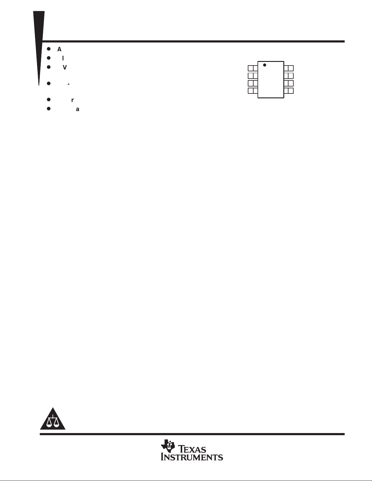
D PACKAGE
(TOP VIEW)
1
2
3
4
8
7
6
5
GND
GND
GND
GND
description
The TPPM0301 is a low-dropout regulator with auxiliary power management that provides a constant 3.3-V
supply at the output capable of driving a 400-mA load.
The TPPM0301 provides a regulated power output for systems that have multiple input sources and require a
constant voltage source with a low-dropout voltage. This is a single output, multiple input intelligent power
source selection device with a low-dropout regulator for either 5VCC or 5VAUX inputs, and a low- resistance
bypass switch for the 3.3VAUX input.
Transitions may occur from one input supply to another without generating a glitch, outside of the specification
range, on the 3.3-V output. The device has an incorporated reverse blocking scheme to prevent excess leakage
from the input terminals in the event that the output voltage is greater than the input voltage.
The input voltage is prioritized in the following order: 5VCC, 5VAUX, and 3.3VAUX.
Please be aware that an important notice concerning availability, standard warranty, and use in critical applications of
Texas Instruments semiconductor products and disclaimers thereto appears at the end of this data sheet.
PRODUCTION DATA information is current as of publication date.
Products conform to specifications per the terms of Texas Instruments
standard warranty. Production processing does not necessarily include
testing of all parameters.
POST OFFICE BOX 655303 • DALLAS, TEXAS 75265
Copyright 2000, Texas Instruments Incorporated
1
Page 2
TPPM0301
I/O
DESCRIPTION
400-mA LOW-DROPOUT REGULATOR
WITH AUXILIARY POWER MANAGEMENT
SLVS315 – SEPTEMBER 2000
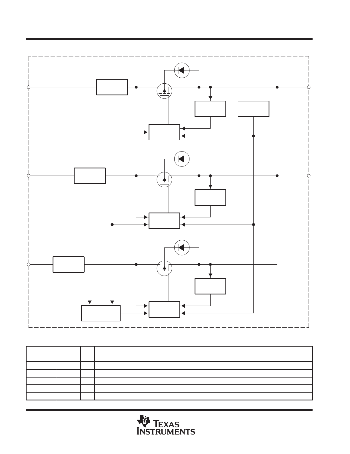
functional block diagram
Linear Regulator
5VCC
5-V
Detection
With LDO
3.3VOUT
5VAUX
3.3VAUX
3VAUX
Detection
5VAUX
Detection
Gate Drive
and Control
Linear Regulator
With LDO
Gate Drive
and Control
Low ON
Resistance
Switch
Current
Sensor
Current
Sensor
Over
Temperature
GND
5-V Detection
and Control
Gate Drive
Terminal Functions
TERMINAL
NAME NO.
3.3VAUX 4 I 3.3-V auxiliary input
3.3VOUT 3 O 3.3-V output with a typical capacitance load of 4.7 µF
5VAUX 1 I 5-V auxiliary input
5VCC 2 I 5-V main input
GND 5, 6, 7, 8 I Ground
2
POST OFFICE BOX 655303 • DALLAS, TEXAS 75265
Current
Sensor
Page 3
TPPM0301
400-mA LOW-DROPOUT REGULATOR
WITH AUXILIARY POWER MANAGEMENT
SLVS315 – SEPTEMBER 2000
Table 1. Input Selection
INPUT VOLTAGE STATUS
5VCC 5VAUX 3.3VAUX 5VCC/5VAUX/3.3VAUX 3.3VOUT IL (mA)
0 0 0 None 0 0
0 0 3.3 3.3VAUX 3.3 375
0 5 0 5VAUX 3.3 400
0 5 3.3 5VAUX 3.3 400
5 0 0 5VCC 3.3 400
5 0 3.3 5VCC 3.3 400
5 5 0 5VCC 3.3 400
5 5 3.3 5VCC 3.3 400
(V)
absolute maximum ratings over operating free-air temperature (unless otherwise noted)
Supply voltage, 5-V main input, V
Auxiliary voltage, 5-V input, V
Auxiliary voltage, 3.3-V input, V
3.3-V output current limit, I
(LIMIT)
(5VCC)
(5V AUX)
(see Notes 1 and 2) 7 V. . . . . . . . . . . . . . . . . . . . . . . . . . . . . . . . . . . . . . .
(3.3V AUX)
1.5 A. . . . . . . . . . . . . . . . . . . . . . . . . . . . . . . . . . . . . . . . . . . . . . . . . . . . . . . . . . .
INPUT SELECTED OUTPUT
(V)
OUTPUT
(I)
†
(see Notes 1 and 2) 7 V. . . . . . . . . . . . . . . . . . . . . . . . . . . . . . . . . . . . .
(see Notes 1 and 2) 5 V. . . . . . . . . . . . . . . . . . . . . . . . . . . . . . . . . . . .
Continuous power dissipation, PD (see Note 3) 1 W. . . . . . . . . . . . . . . . . . . . . . . . . . . . . . . . . . . . . . . . . . . . . . . .
Electrostatic discharge susceptibility, human body model, V
(HBMESD)
2 kV. . . . . . . . . . . . . . . . . . . . . . . . . . . .
Operating ambient temperature range, TA 0°C to 70°C. . . . . . . . . . . . . . . . . . . . . . . . . . . . . . . . . . . . . . . . . . . . . .
Storage temperature range, T
–55°C to 150°C. . . . . . . . . . . . . . . . . . . . . . . . . . . . . . . . . . . . . . . . . . . . . . . . . . .
stg
Operating junction temperature range, TJ –5°C to 120°C. . . . . . . . . . . . . . . . . . . . . . . . . . . . . . . . . . . . . . . . . . . .
Lead temperature (soldering, 10 second), T
†
Stresses beyond those listed under “absolute maximum ratings” may cause permanent damage to the device. These are stress ratings only, and
functional operation of the device at these or any other conditions beyond those indicated under “recommended operating conditions” is not
implied. Exposure to absolute-maximum-rated conditions for extended periods may affect device reliability.
NOTES: 1. All voltage values are with respect to GND.
2. Absolute negative voltage on these terminal should not be below –0.5 V.
3. R
must be less than 55°C/W, typically achieved with two square inches of copper printed circuit board area connected to the GND
θJA
terminals for heat dissipation or equivalent.
260°C. . . . . . . . . . . . . . . . . . . . . . . . . . . . . . . . . . . . . . . . . . .
(LEAD)
recommended operating conditions
5-V main input, V
5-V auxiliary input, V
3.3-V auxiliary input, V
Load capacitance, C
Load current, I
Ambient temperature, T
(5VCC)
(5VAUX)
(3.3VAUX)
L
L
A
POST OFFICE BOX 655303 • DALLAS, TEXAS 75265
MIN TYP MAX UNIT
4.5 5.5 V
4.5 5.5 V
3 3.6 V
4.23 4.7 5.17 µF
0 400 mA
0 70 °C
3
Page 4
TPPM0301
(Q)
y
A
3.3VOUT output shorted to 0 V
°C
400-mA LOW-DROPOUT REGULATOR
WITH AUXILIARY POWER MANAGEMENT
SLVS315 – SEPTEMBER 2000
electrical characteristics over recommended operating free-air temperature range, TA = 0°C to
70°C, C
V
(5VCC)
V
(5VAUX)
I
I
L
I
(LIMIT)
T
(TSD)
T
hys
V
(3.3VOUT)
C
L
I
lkg(REV)
†
Design targets only. Not tested in production.
= 4.7 µF (unless otherwise noted)
L
PARAMETER TEST CONDITIONS MIN TYP MAX UNIT
/
†
†
5-V inputs 4.5 5 5.5 V
Quiescent supply current
Output load current 0.4
Output current limit 3.3VOUT = 0 V 1 1.5
Thermal shutdown
Thermal hysteresis
3.3-V output IL = 400 mA 3.135 3.3 3.465 V
Load capacitance
Reverse leakage output current
From 5VCC or 5VAUX terminals, IL = 0 to
400 mA
From 3.3VAUX terminal, IL = 0 A 250 500 µA
p
Minimal ESR to insure stability of regulated
output
Tested for input that is grounded.
3.3VAUX, 5VAUX or 5VCC = GND,
3.3VOUT = 3.3 V
150 180
2.5 5 mA
15
4.7 µF
°
50 µA
5-V detect
PARAMETER TEST CONDITIONS MIN TYP MAX UNIT
V
(TO_LO)
V
(TO_HI)
Threshold voltage, low 5VAUX or 5VCC ↓ 3.85 4.05 4.25 V
Threshold voltage, high 5VAUX or 5VCC ↑ 4.1 4.3 4.5 V
auxiliary switch
PARAMETER TEST CONDITIONS MIN TYP MAX UNIT
R
(SWITCH)
∆V
O(∆VI)
∆V
O(∆IO)
VI – V
O
Auxiliary switch resistance
Line regulation voltage 5VAUX or 5VCC = 4.5 V to 5.5 V 2 mV
Load regulation voltage 20 mA < IL < 400 mA 40 mV
Dropout voltage IL < 400 mA 1 V
thermal characteristics
R
Thermal impedance, junction-to-case 38 °C/W
θJC
R
Thermal impedance, junction-to-ambient 97 °C/W
θJA
5VAUX = 5VCC = 0 V,
3.3VAUX = 3.3 V, IL = 150 mA
PARAMETER MIN TYP MAX UNIT
0.4 Ω
4
POST OFFICE BOX 655303 • DALLAS, TEXAS 75265
Page 5

TPPM0301
400-mA LOW-DROPOUT REGULATOR
WITH AUXILIARY POWER MANAGEMENT
SLVS315 – SEPTEMBER 2000
THERMAL INFORMATION
T o ensure reliable operation of the device, the junction temperature of the output device must be within the safe
operating area (SOA). This is achieved by having a means to dissipate the heat generated from the junction
of the output structure. There are two components that contribute to thermal resistance. They consist of two
paths in series. The first is the junction to case thermal resistance, R
thermal resistance, R
R
θJA
= R
θJC
+ R
. The overall junction to ambient thermal resistance, R
θCA
θCA
The ability to efficiently dissipate the heat from the junction is a function of the package style and board layout
incorporated in the application. The operating junction temperature is determined by the operating ambient
temperature, T
The junction temperature, T
TJ = TA + PJ (R
TJ = TA + PJ (R
, and the junction power dissipation, PJ.
A
, is equal to the following thermal equation:
J
θJC
θJA
) + PJ (R
)
θCA
)
This particular application uses the enhanced 8-pin SO package with an integral fused lead frame (terminals
5 to 8). By incorporating a dedicated heat spreading copper plane of at least two square inches on a double-side
printed-circuit board (PCB), a thermal resistance of junction to ambient, R
Alternatively, if no dedicated copper plane is incorporated for this device and the PCB has a multilayer
construction, the ground terminals (5 to 8) could be electrically connected to the ground plane of the board. This
will provide a means for heat spreading through the copper plane associated within the PCB (GND layer). This
concept could provide a thermal resistance from junction to ambient, R
Hence, maximum power dissipation allowable for an operating ambient temperature of 70°C, and a maximum
junction temperature of 150°C is determined as:
; the second is the case to ambient
θJC
θJA
, of 70°C/W if implemented correctly .
θJA
, is determined by:
θJA
, of 50°C/W can be obtained.
PJ = (TJ – TA) / R
θJA
PJ = (150 – 70) / 50 = 1.6 W
Using two square inches of dedicated copper plane on double-sided PCB,
= (150 – 70) / 70 = 1.14 W
P
J
Using a multilayer board and utilizing the ground plane for heat spreading, worst case maximum power
dissipation is determined by:
= (5.5 – 3) × 0.4 = 1 W
P
D
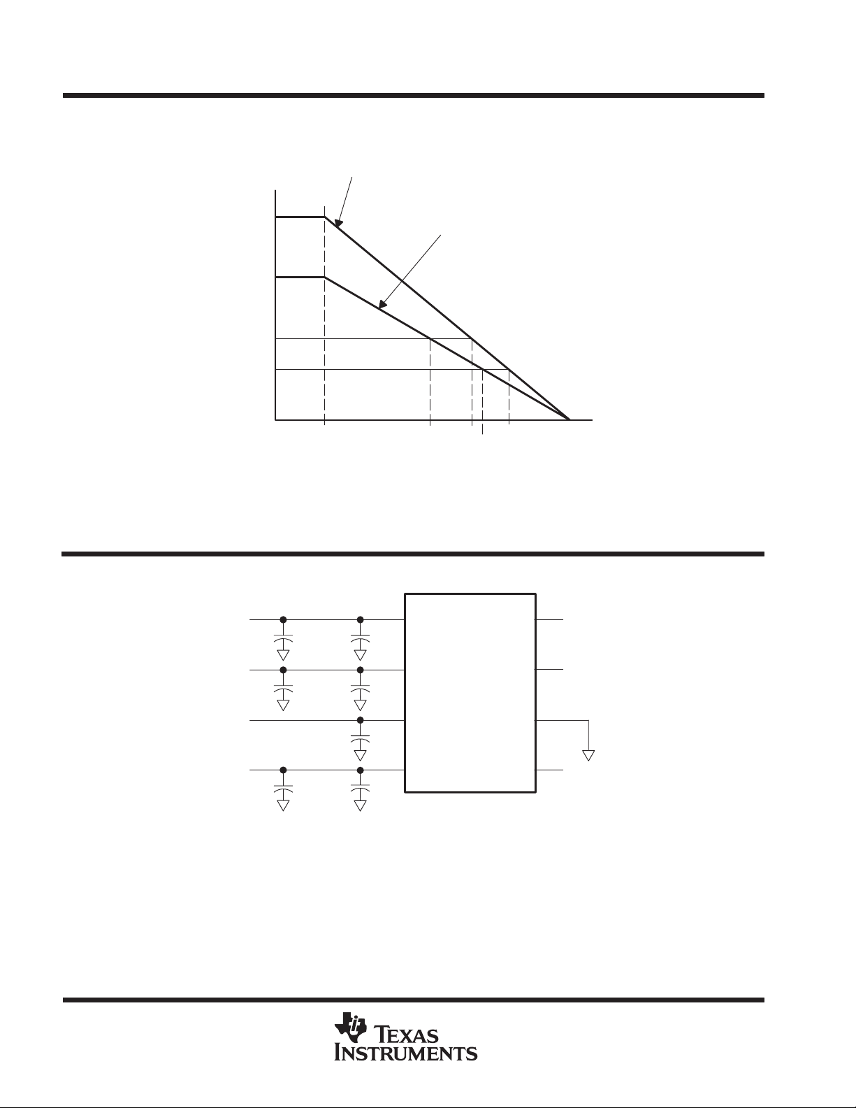
Normal operating maximum power dissipation is (see Figure 1):
PD = (5 – 3.3) × 0.4 = 0.68 W
POST OFFICE BOX 655303 • DALLAS, TEXAS 75265
5
Page 6
TPPM0301
400-mA LOW-DROPOUT REGULATOR
WITH AUXILIARY POWER MANAGEMENT
SLVS315 – SEPTEMBER 2000
THERMAL INFORMATION
Power Dissipation Derate Curve Using
Two Square Inches of Copper Heat
Spreader on a Double-Sided PCB
2.5
1.78
Power – W
1
0.68
Power Dissipation Derate Curve Using
Multilayer Board With The Ground
Plane for Heat Spreader
25
Ambient Temperature – °C
NOTE: These curves are to be used for guideline purposes only . For a particular application, a more specific thermal characterization is required.
80 100
116 150
103
Figure 1. Power Dissipation Derating Curves
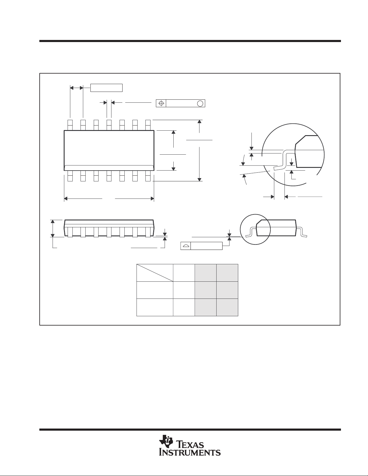
APPLICATION INFORMATION
1
5VAUX GND
4.7 µF
4.7 µF
0.1 µF
0.1 µF4.7 µF
4.7 µF
0.1 µF
5VCC GND
TPPM0301
3.3VOUT GND
3.3VAUX GND
Figure 2. Typical Application Schematic
8
72
63
54
6
POST OFFICE BOX 655303 • DALLAS, TEXAS 75265
Page 7
TPPM0301
400-mA LOW-DROPOUT REGULATOR
WITH AUXILIARY POWER MANAGEMENT
SLVS315 – SEPTEMBER 2000
MECHANICAL DATA
D (R-PDSO-G**) PLASTIC SMALL-OUTLINE PACKAGE
14 PINS SHOWN
0.050 (1,27)
14
1
0.069 (1,75) MAX
0.020 (0,51)
0.014 (0,35)
8
7
A
0.010 (0,25)
0.004 (0,10)
DIM
0.157 (4,00)
0.150 (3,81)
PINS **
0.010 (0,25)
0.244 (6,20)
0.228 (5,80)
8
M
Seating Plane
0.004 (0,10)
14
0.008 (0,20) NOM
0°–8°
16
Gage Plane
0.010 (0,25)
0.044 (1,12)
0.016 (0,40)
A MAX
A MIN
NOTES: A. All linear dimensions are in inches (millimeters).
B. This drawing is subject to change without notice.
C. Body dimensions do not include mold flash or protrusion, not to exceed 0.006 (0,15).
D. Falls within JEDEC MS-012
POST OFFICE BOX 655303 • DALLAS, TEXAS 75265
0.197
(5,00)
0.189
(4,80)
0.344
(8,75)
0.337
(8,55)
0.394
(10,00)
0.386
(9,80)
4040047/D 10/96
7
Page 8

IMPORTANT NOTICE
T exas Instruments and its subsidiaries (TI) reserve the right to make changes to their products or to discontinue
any product or service without notice, and advise customers to obtain the latest version of relevant information
to verify, before placing orders, that information being relied on is current and complete. All products are sold
subject to the terms and conditions of sale supplied at the time of order acknowledgment, including those
pertaining to warranty, patent infringement, and limitation of liability.
TI warrants performance of its semiconductor products to the specifications applicable at the time of sale in
accordance with TI’s standard warranty. Testing and other quality control techniques are utilized to the extent
TI deems necessary to support this warranty . Specific testing of all parameters of each device is not necessarily
performed, except those mandated by government requirements.
Customers are responsible for their applications using TI components.
In order to minimize risks associated with the customer’s applications, adequate design and operating
safeguards must be provided by the customer to minimize inherent or procedural hazards.
TI assumes no liability for applications assistance or customer product design. TI does not warrant or represent
that any license, either express or implied, is granted under any patent right, copyright, mask work right, or other
intellectual property right of TI covering or relating to any combination, machine, or process in which such
semiconductor products or services might be or are used. TI’s publication of information regarding any third
party’s products or services does not constitute TI’s approval, warranty or endorsement thereof.
Copyright 2000, Texas Instruments Incorporated
 Loading...