


www.ti.com
P0021-02
PWP HTSSOP PACKAGE
(TOP VIEW)
SCR1
Cboot2
Cboot1
V
L1
PGND
L2
V
5
A
driver
OUT
Vg
IN
SCR0
5Vg_ENABLE
ENABLE
V
GND
R
REST
A
RESET
CLP
logic
mod
OUT
20
19
18
17
16
15
14
13
12
11
1
2
3
4
5
6
7
8
9
10
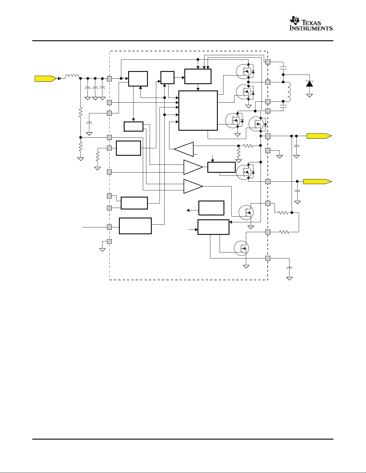
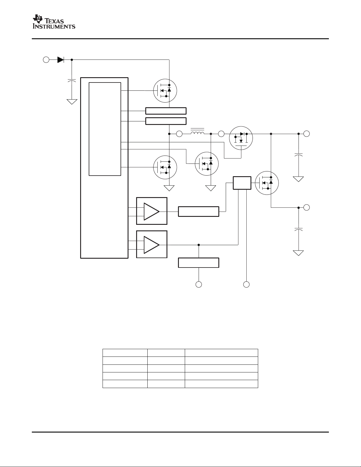
BUCK/BOOST SWITCH-MODE REGULATOR
TPIC74100-Q1
SLIS125 – DECEMBER 2006
FEATURES
• Switch-Mode Regulator
– 5 V ±2%, Normal Mode
– 5 V ±3%, Low-Power or Crossover Mode
• Switching Frequency, 440 kHz (typical)
• Input Operating Range, 1.5 V to 40 V, (V
– 1-A Load-Current Capability
– 200-mA Load-Current Capability Down to
2-V Input (V
– 120-mA Load-Current Capability Down to
1.5-V Input (V
• Enable Function
• Low-Power Operation Mode
)
driver
)
driver
• Switched 5-V Regulated Output on 5Vg With
Current Limit
• Programmable Slew Rate and Frequency
Modulation for EMI Consideration
• Reset Function With Deglitch Timer and
)
driver
Programmable Delay
• Alarm Function for Undervoltage Detection
and Indication
• Thermally Enhanced Package for Efficient
Heat Management
APPLICATIONS
• Automotive Electronic Controller Power
Supply
DESCRIPTION
The TPIC74100-Q1 is a switch-mode regulator with integrated switches for voltage-mode control. With the aid of
external components (LC combination), the device regulates the output to 5 V ±3% for a wide input-voltage
range.
The TPIC74100-Q1 offers a reset function to detect and indicate when the 5-V output rail is outside of the
specified tolerance. This reset delay is programmable using an external timing capacitor on the REST terminal.
Additionally, an alarm (A
value (set by the A
The TPIC74100-Q1 has a frequency-modulation scheme to minimize EMI. The clock modulator permits a
modulation of the switching frequency to reduce interference energy in the frequency band.
The 5Vg output is a switched 5-V regulated output with internal current limiting to prevent RESET from being
asserted when powering a capacitive load on the supply line. This function is controlled by the 5Vg_ENABLE
terminal. If there is a short to ground on this output (5Vg output), the output self-protects by operating in a
chopping mode. This does, however, increase the output ripple voltage on V
PowerPAD is a trademark of Texas Instruments.
All other trademarks are the property of their respective owners.
PRODUCTION DATA information is current as of publication date.
Products conform to specifications per the terms of the Texas
Instruments standard warranty. Production processing does not
necessarily include testing of all parameters.
) feature is activated when the input supply rail V
OUT
terminal).
IN
OUT
driver
during this fault condition.
is below a prescaled specified
Ordering Information
Part Number Package
TPIC74100QPWPRQ1 R-PDSO-G (PWP, 20-pin)
Please be aware that an important notice concerning availability, standard warranty, and use in critical applications of Texas
Instruments semiconductor products and disclaimers thereto appears at the end of this data sheet.
Copyright © 2006, Texas Instruments Incorporated
www.ti.com
B0130-01
Switch-Mode
ControllerWith
Dead Time
Charge
Pump
Vref
Bandgap
Ref
Vreg
Osc
+
-
+
-
PORWith
Delay Timer
V
driver
ENABLE
GND
L1
5VSupply
5Vg_Supply
-
+
L2
V
OUT
Q1
Q2
Q3
Q4
RESET
Temp
Monitor
Shutdown
Regulator
R
mod
Clock
Modulator
Cboot1
Cboot2
5Vg_ENABLE
A
OUT
REST
PGND
SCR0
SCR1
SlewRate
Control
5
Vg
Low-Power
Mode
Control
CLP
Inrush
CurrentLimit
4.7nF
22 H–
100 Hmm
4.7nF
5kW
12kW
R1
R2
L
C
470nF
2.2nF–150nF
Charge
Pump
Bandgap
Ref
V
logic
A
IN
Vbattery
22µF–470µF
1µF–100µF
ExternalSchottky
DiodeRequired,
Max.0.4V
@1 A
@125ºC
Low-PowerMode
DigitalSignal
5kW
TPIC74100-Q1
BUCK/BOOST SWITCH-MODE REGULATOR
SLIS125 – DECEMBER 2006
NOTE: All component values are typical.
2
Submit Documentation Feedback
www.ti.com
Table 1. Terminal Functions
TERMINAL
NAME NO. I/O
SCR1 1 I Programmable slew-rate control
Cboot2 2 I External bootstrap capacitor
Cboot1 3 I External bootstrap capacitor
V
driver
L1 5 I Inductor input (an external Schottky diode
PGND 6 I Power ground
L2 7 I Inductor output
V
OUT
5Vg 9 O Switched 5-V supply
A
IN
CLP 11 I/O Low-power operation mode (digital input)
RESET 12 O Reset function (open drain)
A
OUT
REST 14 O Programmable reset timer delay
R
mod
GND 16 I Ground
V
logic
ENABLE 18 I Switch-mode regulator enable/disable
5Vg_ENABLE 19 I Switched 5-V voltage regulator output enable/disable
SCR0 20 I Programmable slew-rate control
(1) Maximum 0.4 V @ 1 A @ 125°C
4 I Input voltage source
8 O 5-V regulated output
10 I Programmable alarm setting
13 O Alarm output (open drain)
15 I Main switching frequency modulation setting to minimize EMI
17 O Supply decoupling output (may be used as a 5-V supply for logic-level inputs)
Exposed thermal pad of the package should be connected to GND or left floating.
BUCK/BOOST SWITCH-MODE REGULATOR
DESCRIPTION
(1)
to GND must be connected to L1)
TPIC74100-Q1
SLIS125 – DECEMBER 2006
Submit Documentation Feedback
3
www.ti.com
TPIC74100-Q1
BUCK/BOOST SWITCH-MODE REGULATOR
SLIS125 – DECEMBER 2006
ABSOLUTE MAXIMUM RATINGS
over recommended operating free-air temperature range (unless otherwise noted)
Unregulated input voltage, V
Unregulated inputs, V
, V
(AIN)
Bootstrap voltages V
Switch mode voltages V
Logic input voltages, V
Low output voltages, V
(Rmod)
(RESET)
Electrostatic-discharge V
susceptibility
Thermal impedance, junction-to-case, R
Thermal impedance, R
junction-to-ambient
Continuous power dissipation, P
Operating virtual junction temperature range, T
Operating ambient temperature range, T
Storage temperature range, T
Lead temperature (soldering, 10 s), T
(1) Stresses beyond those listed under "absolute maximum ratings" may cause permanent damage to the device. These are stress ratings
only, and functional operation of the device at these or any other conditions beyond those indicated under "recommended operating
conditions" is not implied. Exposure to absolute-maximum-rated conditions for extended periods may affect device reliability.
(2) All voltage values are with respect to ground.
(3) The human body model is a 100-pF capacitor discharged through a 1.5-k Ω resistor into each terminal.
(4) The thermal data is based on using 2-oz. copper trace with at least four square inches of copper footprint for heat dissipation. The
copper pad is soldered to the thermal land pattern. Correct attachment procedure must be incorporated.
(5) The thermal data is based on using 1-oz. copper trace with at least four square inches of copper footprint for heat dissipation. The
copper pad is soldered to the thermal land pattern. Correct attachment procedure must be incorporated.
(2)
(driver)
(2)
(ENABLE)
(Cboot1)
V
(Cboot2)
(L1)
V
(L2)
,V
,V
,V
(4)
(CLP)
, and V
, and V
(5Vg_ENABLE)
(2)
(REST)
J
(SCR0)
(SCR1)
,V
,V
(AOUT)
(logic)
(3)
(HBMESD)
V
(HBMESD)
θ JA
R
θ JA
D
stg
, pin 7 (L2), pin 8 (V
(3)
, pins 1–6 and 10–20 2 kV
θ JC
(4)
(5)
A
(LEAD)
(2)
), pin 9 (5Vg) 800 V
OUT
(1)
–0.5 V to 40 V
–0.5 V to 40 V
See Dissipation
–40°C to 150°C
–40°C to 125°C
–65°C to 125°C
52 V
14 V
–1 V to 40 V
–1 V to 7 V
–0.5 V to 7 V
–0.5 V to 7 V
2°C/W
32°C/W
40°C/W
Rating Table
260°C
DISSIPATION RATING TABLE
R
32°C/W 3.9 W 31.25 mW/°C 2.03 W 0.781 W
40°C/W 3.125 W 25 mW/°C 1.625 W 0.625 W
TA≤ 25°C Power Rating Derating Factor Above TA= 25°C TA= 85°C Power Rating TA= 125°C Power Rating
θ JA
RECOMMENDED OPERATING CONDITIONS
MIN MAX UNIT
Unregulated input voltage, V
Unregulated input voltages, V
Switch-mode terminals V
Bootstrap voltages V
Logic levels (I/O), V
V
(REST)
(Rmod)
Operating ambient temperature range, T
Logic levels (I/O), V
(SCR0)
4
(driver)
and V
(AIN)
, V
(logic)
, V
(SCR1)
(ENABLE)
V
(L1)
V
(L2)
V
(Cboot1)
V
(Cboot2)
,V
,V
(SCR0)
(SCR1)
A
, V
directly connected to V
(CLP)
,V
(5Vg_ENABLE)
,V
, V
(RESET)
(logic)
, V
(AOUT)
, and
(CLP)
Submit Documentation Feedback
6 24 V
0 24 V
–1 17
5 5.5
V
+ 10
(driver)
0 5.25 V
–40 125 °C
V
(logic)
V
(logic)
8
V
www.ti.com
BUCK/BOOST SWITCH-MODE REGULATOR
ELECTRICAL CHARACTERISTICS
V
= 6 V to 17 V, TA= -40°C to 125°C, unless otherwise noted
(driver)
Parameters TEST CONDITIONS Min Typ Max Unit
V
(driver)
V
(driver)
S
OM
I
(standby)
I
q
V
O
V
O
I
O
I
O(Boost)
I
PPn
I
PPl
I
P
V
(driver)
T
ot
5Vg Output and ENABLE
r
DS(on)
I
O
V
I
V
IH
V
IL
V
(hys)
r
(pd)
ENABLE
V
I
V
IH
V
IL
V
(hys)
(1) Ensured by characterization.
(2) Tested with inductor having following characteristics: L = 33 µH, R
when inductor R
(3) Ensured by characterization. For further details, see the Buck/Boost Transitioning section.
(4) Ensured by characterization; hysteresis 15°C (typical)
Unregulated input voltage 1.5 40 V
Start-up condition voltage IO= 600 mA 5 V
CO= 36 µF (min) to 220 µF (max) 4 20
Soft-start ramp V/ms
CO= 220 µF (min) to 470 µF (max), see
(1)
Note
Standby current ENABLE = low 10 20 µA
Quiescent current CLP = 0 V, V
= 11 V, IO= 0 mA 100 160 µ A
(driver)
Output voltage DC 5 V
Normal mode 2%
Output-voltage tolerance
Boost/buck crossover or low-power
mode
Output current V
Output current, boost mode mA
Internal peak current limit (normal
mode)
Internal peak current limit (low-power
mode)
Peak current V
Boost/buck crossover voltage
window
Thermal shutdown
(4)
≥ 7 V 1 A
(driver)
V
= 2 V, see Note
(driver)
V
= 1.5 V, see Note
(driver)
(1)
(1)
= 16 V, IO= 1 A, and L = 33 µH 1.5 A
(driver)
See Note
(3)
On-state resistance 135 225 m Ω
Output current 400 mA
5Vg_ENABLE input-voltage range –0.5 V
5Vg_ENABLE threshold high voltage V
5Vg_ENABLE threshold low voltage V
= 5 V 2.5 3 3.5 V
(5Vg)
= 0 V 1.5 2 2.5 V
(5Vg)
Hysteresis voltage 0.5 1 V
Internal pulldown resistor 300 500 850 k Ω
ENABLE input-voltage range –0.5 40 V
ENABLE threshold high voltage V
8 V ≤ V
6 V ≤ V
≤ 17 V 2.5 3 3.5
(driver)
< 8 V 1.9 3 3.5
(driver)
ENABLE threshold low voltage VO= 5 V 1.5 2 2.5 V
Hysteresis voltage V
(ESR) is increased.
max
8 V ≤ V
6 V ≤ V
≤ 17 V 0.5 1
(driver)
< 8 V 0.1
(driver)
= 0.1 Ω , IR= 1.8 A. Output current must be verified in application
max
TPIC74100-Q1
SLIS125 – DECEMBER 2006
2 20
3%
(2)
(2)
1.75 2.5 A
0.75 1.25
5 5.9 V
160 180 200 °C
200
120
O
V
Submit Documentation Feedback
5

www.ti.com
TPIC74100-Q1
BUCK/BOOST SWITCH-MODE REGULATOR
SLIS125 – DECEMBER 2006
ELECTRICAL CHARACTERISTICS (continued)
V
= 6 V to 17 V, TA= -40°C to 125°C, unless otherwise noted
(driver)
Parameters TEST CONDITIONS Min Typ Max Unit
RESET
V
(th)
V
(RESET)
t
(RESET)
V
OL
t
(deglitch)
Alarm
V
I
V
IL
V
IH
V
(hys)
V
OL
Low-Power Mode (Pulse Mode) PFM
I
O(LPM)
I
I(avg)
V
O
Digital Low-Power Mode (CLP)
V
IH
V
IL
Switching Parameters
f
(sw)
f
(sw)ac
f
(sw)min
f
(sw)max
f
(mod)span
f
(mod)
f
(mod)ac
RESET threshold voltage 4.51 4.65 4.79 V
RESET tolerance 3%
RESET time ms
RESET output low voltage mV
RESET deglitch time See Note
Alarm input-voltage range –0.5 40 V
Alarm threshold low voltage 2.2 2.3 2.35 V
Alarm threshold high voltage 2.43 2.5 2.58 V
Hysteresis voltage 200 mV
Alarm output low voltage mV
Load current in low-power mode V
Average input current V
Output-voltage tolerance VO= 5 V 2.4% 3%
High-level CLP input threshold
voltage
Low-level CLP input threshold
voltage
Switching frequency V
Operating-frequency accuracy
Modulation minimum frequency 270 330 445 kHz
Modulation maximum frequency 450 550 680 kHz
Modulation span 220 kHz
Modulation frequency R
Modulation-frequency accuracy 12%
C
= 10 nF 8 10 12
(REST)
C
= 100 nF, see Note
(REST)
I
= 5 mA 450
sink
I
= 1 mA 84
sink
I
sink
I
sink
(5)
= 5 mA 450
= 1 mA 84
< 7 V 50 mA
(driver)
= 11 V, IO= 5 mA, CLP = low 3.55 mA
(driver)
(5)
80 100 120
8 10 12.5 µs
Normal mode 2.6 V
Low-power mode 1.15 V
= 0 V, modulator OFF 440 kHz
(Rmod)
f
= 440 kHz 18%
(sw)
f
= 440 kHz 20%
(sw)
= 12 k Ω ±1% 28 kHz
mod
(5) Ensured by characterization.
6
Submit Documentation Feedback

www.ti.com
I
OUT
D * D
2
Ǹ
Upper:
Lower:
V =2.5V×
(driver)
R1+R2
R1
V =2.3V×
(driver)
R1+R2
R1
.
TPIC74100-Q1
BUCK/BOOST SWITCH-MODE REGULATOR
SLIS125 – DECEMBER 2006
PRINCIPLES OF OPERATION
Functional Principle
The TPIC74100-Q1 is a buck/boost switch-mode regulator that operates in a power-supply concept to ensure a
stable output voltage with input voltage excursions and specified load range.
The device provides an alarm indicator and reset output to interface with systems that require supervisory
function.
The switching regulator offers a clock modulator and a current-mode slew-rate control for the internal switching
transistor (Q1) to minimize EMI.
An internal low-r
output.
Description of the Functional Terminals
Switch-Mode Input/Output Terminals (L1, L2)
The external inductor for the switch-mode regulator is connected between terminals L1 and L2. This inductor is
placed close to the terminals to minimize parasitic effects. For stability, an inductor with 20 µ H to 100 µ H should
be used.
switch has a current-limit feature to prevent inadvertent reset when turning on the 5Vg
DS(on)
Supply Terminal (V
The input voltage of the device is connected to the V
)
driver
terminal. This input line requires a filter capacitor to
driver
minimize noise. A low-ESR aluminum or tantalum input capacitor is recommended. The relevant parameters for
the input capacitor are the voltage rating and RMS current rating. The voltage rating should be approximately
1.5 times the maximum applied voltage for an aluminum capacitor and 2 times for a tantalum capacitor. In buck
mode, the RMS current is
reached when D = 50% with I
RMS
, where D is the duty cycle and its maximum RMS current value is
= I
/2. In boost mode, the RMS current is 0.3 × ∆ I, where ∆ I is the
OUT
peak-to-peak ripple current in the inductor. To achieve this, ESR ceramic capacitors are used in parallel with the
aluminum or tantalum capacitors.
Internal Supply Decoupling Terminal (V
The V
terminal is used to decouple the internal power-supply noise by use of a 470-nF capacitor. This
logic
)
logic
terminal can also be used as an output supply for the logic-level inputs for this device (SCR0, SCR1, ENABLE,
CLP, and 5Vg_ENABLE).
Input Voltage Monitoring Terminal (A
The A
terminal is used to program the threshold voltage for monitoring and detecting undervoltage conditions
IN
)
IN
on the input supply. A maximum of 40 V may be applied to this terminal and the voltage at this terminal may
exceed the V
input voltage without effecting the device operation. The resistor divider network is
(driver)
programmed to set the undervoltage detection threshold on this terminal (see the application schematic). The
input has a typical hysteresis of 200 mV with a typical upper limit threshold of 2.5 V and a typical lower limit
threshold of 2.3 V. When V
falls below 2.3 V, V
(AIN)
is asserted low; when V
(AOUT)
exceeds 2.5 V, V
(AIN)
(AOUT)
the high-impedance state.
The equations to set the upper and lower thresholds of V
are:
(AIN)
is in
Submit Documentation Feedback
7
www.ti.com
TPIC74100-Q1
BUCK/BOOST SWITCH-MODE REGULATOR
SLIS125 – DECEMBER 2006
PRINCIPLES OF OPERATION (continued)
Input Undervoltage Alarm Terminal (A
The A
on the A
terminal is an open-drain output that asserts low when the input voltage falls below the set threshold
OUT
input.
IN
Reset Delay Timer Terminal (REST)
The REST terminal sets the desired delay time to assert the RESET terminal low after the 5-V supply has
exceeded 4.65 V (typical). The delay can be programmed in the range of 2.2 ms to 150 ms using capacitors in
the range of 2.2 nF to 150 nF. The delay time is calculated using the following equation:
RESET delay = C
(REST)
× 1 ms, where C
Reset Terminal (RESET)
The RESET terminal is an open-drain output. The power-on reset output is asserted low until the output voltage
exceeds the 4.65-V threshold and the reset delay timer has expired. Additionally, whenever the ENABLE
terminal is low, RESET is immediately asserted low regardless of the output voltage.
)
OUT
has nF units
(REST)
Main Regulator Output Terminal (V
The V
terminal is the output of the switch-mode regulated supply. This terminal requires a filter capacitor with
OUT
)
OUT
low-ESR characteristics to minimize output ripple voltage. For stability, a capacitor with 22 µ F to 470 µ F should
be used. The total capacitance at pin V
and pin 5Vg must be less than or equal to 470 µ F.
OUT
Low-Power-Mode Terminal (CLP)
The CLP terminal controls the low-power mode of the device. An external low digital signal switches the device
to low-power mode or normal mode when the input is high.
Switch-Output Terminal (5Vg)
The 5Vg terminal switches the 5-V regulated output. The output voltage of the regulator can be enabled or
disabled using this low-r
internal switch. This switch has a current-limiting function to prevent generation of
DS(on)
a reset signal at turnon caused by the capacitive load on the output or overload condition. When the switch is
enabled, the regulated output may deviate and drop momentarily to a tolerance of 7% until the 5Vg capacitor is
fully charged. This deviation depends on the characteristics of the capacitors on V
and 5Vg.
OUT
5Vg-Enable Terminal (5Vg_ENABLE)
The 5Vg_ENABLE is a logic-level input for enabling the switch output on 5Vg.
For the functional terminal, 5Vg_ENABLE results in the following table:
5Vg_ENABLE Function
0 5Vg is off
Open (internal pulldown = 500 k Ω ) 5Vg is off
1 5Vg is on
8
Submit Documentation Feedback
www.ti.com
S0174-01
5Vg_ENABLE
Switch
Control
PeakCurrentLimit
Gate
Driver
5
Vg
Q1
Q2
Q3
Q4
V
driver
L1 L2
33µH
V
OUT
V
OUT
47µF
100µF
5
Vg
SlewRateControl
RESET
ChargePump
RESET Deglitch
RESET
typ~V – 100mV
OUT
V
OUT
typ4.65V
Buck/Boost
GateDriver
BUCK/BOOST SWITCH-MODE REGULATOR
TPIC74100-Q1
SLIS125 – DECEMBER 2006
Figure 1. Current-Limit Switched Output 5Vg
Slew-Rate Control Terminals (SCR0, SCR1)
The slew rate of the switching transistor Q1 is set using the SCR0 and SCR1 terminals.
The following table shows the values of the slew rate (SR):
SCR1 SCR0 SR
0 0 Slow
0 1 Medium-slow
1 0 Medium-fast
1 1 Fast
Q1
Submit Documentation Feedback
9

www.ti.com
TPIC74100-Q1
BUCK/BOOST SWITCH-MODE REGULATOR
SLIS125 – DECEMBER 2006
See the converter efficiency plots in the Typical Characteristics section to determine power dissipation.
Modulator Frequency Setting (Terminal R
The R
terminal adjusts the clock modulator frequency. A resistor of R
mod
frequency of 28 kHz. The modulator function may be disabled by connecting R
)
mod
= 12 k Ω generates a modulation
mod
to GND and the device
mod
operates with the nominal frequency. The modulator function cannot be activated during IC operation, only at IC
start-up.
Ground Terminal (PGND)
The PGND terminal is the power ground for the device.
Enable Terminal (ENABLE)
The ENABLE terminal allows the enabling and disabling of the switch mode regulator. A maximum of 40 V may
be applied to this terminal to enable the device and increasing it above the V
input voltage does not affect
(driver)
the device operation.
The functionality of the ENABLE terminal is described in the following table:
ENABLE Function
0 Vreg is off.
Open Undefined
1 Vreg is on.
Bootstrap Terminals (Cboot1 and Cboot2)
An external bootstrap capacitor is required for driving the internal high-side MOSFET switch. A 4.7-nF ceramic
capacitor is typically required.
Functional Modes
Clock Modulator
To minimize EMI issues associated with the switch-mode regulator, the device offers an integrated clock
modulator. The function of the clock modulator is to modulate the switching frequency and to distribute the
energy over the wave band.
The average switching frequency is 440 kHz (typical) and varies between 330 kHz and 550 kHz at a rate set by
the R
clock modulator function can only be activated during IC start-up, not during IC operation.
The equation for the modulation frequency is as follows:
f
(mod)
Buck/Boost Transitioning
The operation mode switches automatically between buck and boost modes depending on the input voltage of
V
(driver)
boost mode and continues to run in boost mode until V
over to buck mode. In buck mode, the device continues to run in buck mode until it is required to switch back to
boost to hold regulation. This crossover window to switch to boost mode is when V
5 V and depends on the loading conditions. When V
(~2%), the device remains in buck mode. However, when V
drops to 4.9 V, the device crosses over to boost mode to hold regulation. In boost mode, the device remains in
boost mode until V
resistor. A typical value of 12 k Ω on the R
mod
(Hz) = (–2.2 × R
) + 54.5 kHz, when R
mod
= 8 k Ω to 16 k Ω
mod
and output load conditions. During start up, when V
exceeds 5.8 V; at which time, the device enters the buck mode. When the device is
(driver)
terminal relates to a 28-kHz modulation frequency. The
mod
is less than 5.8 V (typical), the device starts in
(driver)
exceeds 5.8 V; at which time, the device switches
(driver)
is between 5.8 V and
drops below 5.8 V but the device is holding regulation
driver
is within the 5.8-V to 5-V window and V
(driver)
(driver)
OUT
10
Submit Documentation Feedback

www.ti.com
S0182-01
Switch
Control
Current
Control
FB
SMPS
Q1
Q2
Q3
Q4
Input
Voltage
L1
L2
33µH
V
driver
V
OUT
22µF–470µF
BUCK/BOOST SWITCH-MODE REGULATOR
TPIC74100-Q1
SLIS125 – DECEMBER 2006
operating in boost mode and V
is in the crossover window of 5.8 V to 5 V, the output regulation may
(driver)
contain a higher than normal ripple and only maintain a 3% tolerance. This ripple and tolerance depends on the
loading and improves with a higher loading condition. When the device is operated with low-power mode active
(CLP = low) and high output currents (>50 mA), the buck/boost transitioning can cause a reset signal at the
RESET pin.
Buck SMPS
In buck mode, the duty cycle of transistor Q1 sets the voltage V
to 99% depending on the input voltage, V
. If the peak inductor current (measured by Q1) exceeds 450 mA
(driver)
. The duty cycle of transistor Q1 varies 10%
OUT
(typical), Q2 is turned on for this cycle (synchronized rectification). Otherwise, the current recirculates through
Q2 as a free-wheeling diode. The detection for synchronous or asynchronous mode is done cycle-by-cycle.
To avoid a cross-conduction current between Q1 and Q2, an inherent delay is incorporated when switching Q1
off and Q2 on and vice versa.
In buck mode, transistor Q3 is not required and is switched off. Transistor Q4 is switched on to reduce power
dissipation.
The switch timings for transistors Q3 and Q4 are not considered. In buck mode, the logical control of the
transistors does not change.
Figure 2. Buck/Boost Switch Mode Configuration
Boost SMPS
In boost mode, the duty cycle of transistor Q3 controls the output voltage V
adjusted 5% to 85% depending on the internally sensed voltage of the output. Synchronized rectification occurs
when V
(driver)
is below 5 V.
. The duty cycle is internally
OUT
To avoid a discharging of the buffer capacitor, a simultaneous switching on of Q3 and Q4 is not allowed. An
inherent delay is incorporated between Q3 switching off and Q4 switching on and vice versa.
In boost mode, transistor Q2 is not required and remains off. Transistor Q1 is switched on for the duration of the
boost-mode operation (serves as a supply line).
Submit Documentation Feedback
11

www.ti.com
TPIC74100-Q1
BUCK/BOOST SWITCH-MODE REGULATOR
SLIS125 – DECEMBER 2006
The switch timings of transistors Q1 and Q2 are not considered. In boost mode, the logical control of the
transistors does not change.
Extension of the Input Voltage Range on V
To ensure a stable 5-V output voltage with the output load in the specified range, the V
(driver)
supply must be
(driver)
greater than or equal to 5 V for greater than 1 ms (typical). After a period of 1 ms (typical), the logic may be
supplied by the V
The switch-mode regulator does not start at V
regulator and the V
OUT
supply may be capable of operating down to 1.5 V.
(driver)
less than 5 V.
(driver)
Low-Power Mode
To reduce quiescent current and to provide efficient operation, the regulator enters a pulsed mode.
The device enters this mode by a logic-level low on this terminal.
Automatic low-power mode is not available.The low-power-mode function is not available in boost mode. The
device leaves low-power mode during boost mode regardless of the logic level on the CLP terminal.
Temperature and Short-Circuit Protection
To prevent thermal destruction, the device offers overtemperature protection to disable the IC. Also, short-circuit
protection is included for added protection on V
and 5Vg.
OUT
Switch Output Terminal (5Vg) Current Limitation
A charge pump drives the internal FET, which switches the primary output voltage V
OUT
to the 5Vg pin.
Protection is implemented to prevent the output voltage from dropping below its specified value while enabling
the secondary output voltage. An explanation of the block diagram (see Figure 1) is given by the following
example:
• Device is enabled, output voltage V
is up and stable.
OUT
• 5Vg is enabled (pin 5Vg_ENABLE set to high) with load resistance connected to 5Vg pin.
• If output voltage V
drops below typical ( V
OUT
– 100 mV), the charge pump of the 5Vg FET is switched off
OUT
and the FET remains on for a while as the gate voltage drops slowly.
• If V
drops below the RESET threshold of 4.65 V (typical), the FET of the secondary output voltage 5Vg is
OUT
switched off (gate drawn to ground level).
• A deglitch time ensures that a device reset does not occur if V
drops to the reset level during the 5Vg
OUT
turnon phase.
• If V
rises above typical (V
OUT
– 100 mV), the charge pump of the 5Vg FET is switched on and drives the
OUT
gate of the 5Vg FET on.
Soft Start
On power up, the device offers a soft-start feature which ramps the output of the regulator at a slew of 10 V/ms.
When a reset occurs, the soft start is reenabled. Additionally, if the output capacitor is greater than 220 µF
(typical), the slew rate decreases to a value set by the internal current limit. In boost mode, the soft-start feature
is not active.
12
Submit Documentation Feedback

www.ti.com
IO − Output Current − mA
0
1
2
3
4
5
6
0 1 2 3 4 5 6 7 8 9 10
I
I
− Input Current − mA
G001
TA = 25°
Maximum
TA = 125°
V
(driver)
= 11 V
IO − Output Current − mA
0.0
0.1
0.2
0.3
0.4
0.5
0.6
0.7
0.8
0.9
1.0
0.0 0.1 0.2 0.3 0.4 0.5 0.6 0.7 0.8 0.9 1.0
I
I
− Input Current − mA
G002
TA = 125°
TA = 25°
Maximum
V
(driver)
= 11 V
TPIC74100-Q1
BUCK/BOOST SWITCH-MODE REGULATOR
SLIS125 – DECEMBER 2006
TYPICAL CHARACTERISTICS
NOTE: Maximum characteristic specified by design.
NOTE: Maximum characteristic specified by design.
Figure 3. Low-Power Mode Current, IO= 0 mA–10 mA
Figure 4. Low-Power-Mode Current, IO= 0 mA–1 mA
Submit Documentation Feedback
13

www.ti.com
VI − Input Voltage − V
0
100
200
300
400
500
600
700
800
900
1000
1100
1.5 2.0 2.5 3.0 3.5 4.0 4.5 5.0 5.5 6.0 6.5 7.0 7.5 8.0 8.5 9.0 9.5 10.0
I
O
− Output Current − mA
G003
TA = 25°
TA = 125°
IO − Output Current − mA
50
55
60
65
70
75
80
85
100 150 200 250 300 350 400 450 500 550 600
Efficiency − %
G004
SCR: 11, V
(driver)
= 11 V
SCR: 10, V
(driver)
= 11 V
SCR: 01, V
(driver)
= 11 V
SCR: 00, V
(driver)
= 11 V
SCR: 11, V
(driver)
= 17 V
SCR: 10, V
(driver)
= 17 V
SCR: 01, V
(driver)
= 17 V
SCR: 00, V
(driver)
= 17 V
TPIC74100-Q1
BUCK/BOOST SWITCH-MODE REGULATOR
SLIS125 – DECEMBER 2006
TYPICAL CHARACTERISTICS (continued)
NOTES:
(1) Typical representation of input voltage vs output load current at TA= 25°C and 125°C, after the correct power-up sequence is
invoked.
(2) The dip in the output current at 5.8 V is caused by the buck/boost transition of the IC.
(3) The output current is clipped to 1 A by the measurement setup.
Figure 5. Typical Input Voltage (V
vs
Maximum Output Load Current (IO)
)
(driver)
NOTE: The average converter efficiency with four different slew rate controls (SCRx) on the Q1 switching FET with input voltage
V
(driver)
14
= 11 V and 17 V, TA= 125°C.
Submit Documentation Feedback
Figure 6. Converter Efficiency

www.ti.com
V(L1)
InputCurrent
(200mA/div)
G005
G010
BUCK/BOOST SWITCH-MODE REGULATOR
TYPICAL CHARACTERISTICS (continued)
Figure 7. Input Current With Slope Control, SCR0 = 0, SCR1 = 0,
Input-Current Slew Rate = 2.8 A/µs, IL= 500 mA, V
= 15 V
(driver)
TPIC74100-Q1
SLIS125 – DECEMBER 2006
Figure 8. Input Current With Slope Control, SCR1 = 0, SCR0 = 1,
Input-Current Slew Rate = 6.25 A/µs, IL= 500 mA, V
= 15 V
(driver)
Submit Documentation Feedback
15

www.ti.com
G011
G008
TPIC74100-Q1
BUCK/BOOST SWITCH-MODE REGULATOR
SLIS125 – DECEMBER 2006
TYPICAL CHARACTERISTICS (continued)
Figure 9. Input Current With Slope Control, SCR1 = 1, SCR0 = 0,
Input-Current Slew Rate = 9.4 A/µs, IL= 500 mA, V
= 15 V
(driver)
Figure 10. Input Current With Slope Control, SCR0 = 1, SCR1 = 1,
Input-Current Slew Rate = 18.8 A/µs, IL= 500 mA, V
16
Submit Documentation Feedback
= 15 V
(driver)

www.ti.com
G009
G012
BUCK/BOOST SWITCH-MODE REGULATOR
TYPICAL CHARACTERISTICS (continued)
Figure 11. Low-Power-Mode Operation, IL= 15 mA, CO= 47 µF
TPIC74100-Q1
SLIS125 – DECEMBER 2006
Figure 12. Nominal Switching Frequency of Q1 Switch (446 kHz)
Submit Documentation Feedback
17

www.ti.com
G013
G006
TPIC74100-Q1
BUCK/BOOST SWITCH-MODE REGULATOR
SLIS125 – DECEMBER 2006
TYPICAL CHARACTERISTICS (continued)
With Modulation Function Disabled, IL= 200 mA
(Reference L1 Terminal, see Figure 13 through Figure 15 )
Figure 13. Minimum Switching Frequency (333 kHz)
With Modulation Enabled, R
Figure 14. Maximum Switching Frequency (555 kHz)
With Modulation Enabled, R
= 12 k Ω , IL= 200 mA
mod
= 12 k Ω , IL= 200 mA
mod
18
Submit Documentation Feedback

www.ti.com
G007
VO
11V,IL =700mA
5V,IL =700mA
2V,IL =225mA
V(driver)
G014
TYPICAL CHARACTERISTICS (continued)
(Reference L1 Terminal, see Figure 13 through Figure 15 )
Figure 15. Modulation Frequency (Full Span) of 28 kHz
TPIC74100-Q1
BUCK/BOOST SWITCH-MODE REGULATOR
SLIS125 – DECEMBER 2006
Figure 16. Input Voltage Excursions (Similar to Low-Crank Conditions)
Submit Documentation Feedback
19

www.ti.com
G015
G016
TPIC74100-Q1
BUCK/BOOST SWITCH-MODE REGULATOR
SLIS125 – DECEMBER 2006
TYPICAL CHARACTERISTICS (continued)
(Reference L1 Terminal, see Figure 13 through Figure 15 )
Figure 17. Switch-Mode Regulator Transition From Buck Mode to Boost Mode, IL= 400 mA
Figure 18. Switch-Mode Regulator Transition From Boost Mode to Buck Mode, IL= 400 mA
20
Submit Documentation Feedback

www.ti.com
LO G 1 0 d B/ div
ModulationOff
Modulation=28kHz
G017
LO G 1 0 d B/ div
SlewRate=11
SlewRate=00
G018
TPIC74100-Q1
BUCK/BOOST SWITCH-MODE REGULATOR
SLIS125 – DECEMBER 2006
TYPICAL CHARACTERISTICS (continued)
(Reference L1 Terminal, see Figure 13 through Figure 15 )
NOTE: These values represent conducted EMI results of a test board for display purposes only. Actual results may vary greatly
depending on board layout and external components and must be verified in actual application.
Figure 19. Conducted Emissions on Test Board Showing Effects of Switching-Frequency Modulation
NOTE: These values represent conducted EMI results of a test board for display purposes only. Actual results may vary greatly
depending on board layout and external components and must be verified in actual application.
Figure 20. Conducted Emissions on Test Board Showing Effects of Minimum and Maximum Slew Rate Settings
Submit Documentation Feedback
21

www.ti.com
M0026-01
PackageThermalPad
SolderPad(LandPattern)
ThermalVias
PackageOutline
M0027-01
PowerPad
PackageSolderPad
PackageSolderPad
(BottomTrace)
ThermalVia
ComponentTraces
ThermalIsolation
PowerPlaneOnly
1,5748mm
0-mm 0,071-mmBoard
Base–andBottomPad
0,5246-mm 0,5606-mm–
PowerPlane
(1-oz.Cu)
1,0142-mm 1,0502-mm–
GroundPlane
(1-oz.Cu)
1,5038-mm 1,5748-mm–
ComponentTrace
(2-oz.Cu)
2Plane
4Plane
TPIC74100-Q1
BUCK/BOOST SWITCH-MODE REGULATOR
SLIS125 – DECEMBER 2006
APPLICATION INFORMATION
To maximize the efficiency of this package for application on a single-layer or multilayer PCB, certain guidelines
must be followed when laying out this device on the PCB.
The following information is to be used as a guideline only.
For further information see the PowerPAD Thermally Enhanced Package technical brief (SLMA002 ).
The following are guidelines for mounting the PowerPAD™ IC on a multilayer PCB with a ground plane.
Figure 21. Package and PCB Land Configuration for a Multilayer PCB
Figure 22. Multilayer Board (Side View)
In a multilayer board application, the thermal vias are the primary method of heat transfer from the package
thermal pad to the internal ground plane.
The efficiency of this method depends on several factors (die area, number of thermal vias, thickness of copper,
etc.). See the PowerPAD Thermally Enhanced Package technical brief (SLMA002).
22
Submit Documentation Feedback

www.ti.com
M0028-01
UseasMuchCopper Area
asPossibleforHeatSpread
PackageThermalPad
PackageOutline
TPIC74100-Q1
BUCK/BOOST SWITCH-MODE REGULATOR
SLIS125 – DECEMBER 2006
APPLICATION INFORMATION (continued)
Figure 23. Land Configuration for Single-Layer PCB
Layout recommendation is to use as much copper area for the power-management section of a single-layer
board as possible. In a single-layer board application, the thermal pad is attached to a heat spreader (copper
areas) by using a low-thermal-impedance attachment method (solder paste or thermal-conductive epoxy). In
both of these cases, it is advisable to use as much copper and as many traces as possible to dissipate the heat.
IMPORTANT
When this attachment method is not implemented correctly, this product may operate inefficiently. Power dissipation capability
may be adversely affected when the device is incorrectly mounted onto the circuit board.
Submit Documentation Feedback
23

www.ti.com
S0183-01
GND
R
mod
REST
A
IN
V
driver
Cboot2
Cboot1
L1 L2
V
OUT
PGND
RESET
SCR1
SCR0
TPIC74100B
ENABLE
V
logic
A
OUT
5V
Vbattery
5V
5Vg_ENABLE
5
Vg
5V
CLP
4.7nF4.7nF
L
C
R2
R1
470nF
2.2nF–150nF
Optional
Connection
5kW
5kW
1 µF–100µF
22µF–470µF
12 kW
22µH–100µH
TPIC74100-Q1
BUCK/BOOST SWITCH-MODE REGULATOR
SLIS125 – DECEMBER 2006
A. To minimize voltage ripple on the output due to transients, it is recommended to use a low-ESR capacitor on the
V
line.
OUT
B. The L and C component values are system application dependent for EMI consideration.
Layout Guidelines for Switch-Mode Power Supply
The following guidelines are recommended for PCB layout of the TPIC74100-Q1 device.
Inductor
Use a low-EMI inductor with a ferrite-type closed core. Other types of inductors may be used; however, they
must have low-EMI characteristics and be located away from the low-power traces and components in the
circuit.
Filter Capacitors
Input ceramic filter capacitors should be located in the close proximity of the V
capacitors are recommended to minimize lead length and reduce noise coupling.
Traces and Ground Plane
All power (high-current) traces should be thick and as short as possible. The inductor and output capacitors
should be as close to each other as possible. This reduces EMI radiated by the power traces due to high
switching currents.
24
Figure 24. Application Schematic
Submit Documentation Feedback
driver
terminal. Surface-mount

www.ti.com
L +
ǒ
VIN* V
OUT
Ǔ
V
OUT
fSW DIL V
IN
I
L,max
+ I
OUT
)
DI
L
2
DV
OUT
+ DI
L
ǒ
ESR )
1
8 f
SW
C
OUT
Ǔ
C
OUT
+
I
pk
(
ton) t
off
)
8 V
ripple
L +
ǒ
V
OUT
* V
IN
Ǔ
V
IN
fSW DIL V
OUT
Ip+ I
L,max
+ I
IN
)
DI
L
2
DV
OUT
+ Ip ESR)
I
OUT
ǒ
1 *
V
IN
V
OUT
Ǔ
fSW C
OUT
TPIC74100-Q1
BUCK/BOOST SWITCH-MODE REGULATOR
SLIS125 – DECEMBER 2006
In a two-sided PCB, it is recommended to have ground planes on both sides of the PCB to help reduce noise
and ground-loop errors. The ground connection for the input and output capacitors and IC ground should be
connected to this ground plane.
In a multilayer PCB, the ground plane is used to separate the power plane (where high switching currents and
components are placed) from the signal plane (where the feedback trace and components are) for improved
performance.
Also, arrange the components such that the switching-current loops curl in the same direction. Place the
high-current components such that during conduction, the current path is in the same direction. This prevents
magnetic field reversal caused by the traces between the two half-cycles, helping to reduce radiated EMI.
Buck Mode
• Select inductor ripple current DIL: for example ∆ IL= 0.2 × I
• Calculate inductor L:
where fSWis the regulator switching frequency.
• Inductor peak current:
• Output voltage ripple:
OUT
(1)
(2)
Usually, the first term is dominant.
Boost Mode
• Select inductor ripple current ∆ IL: for example ∆ IL= 0.2 × I
• Calculate inductor L:
where fSWis the regulator switching frequency.
• Inductor peak current:
• Output voltage ripple:
(3)
(4)
IN
(5)
(6)
(7)
Submit Documentation Feedback
25

PACKAGE OPTION ADDENDUM
www.ti.com
10-Dec-2007
PACKAGING INFORMATION
Orderable Device Status
(1)
Package
Type
Package
Drawing
Pins Package
Qty
Eco Plan
TPIC74100QPWPRQ1 ACTIVE HTSSOP PWP 20 1 Green (RoHS &
no Sb/Br)
(1)
The marketing status values are defined as follows:
ACTIVE: Product device recommended for new designs.
LIFEBUY: TI has announced that the device will be discontinued, and a lifetime-buy period is in effect.
NRND: Not recommended for new designs. Device is in production to support existing customers, but TI does not recommend using this part in
a new design.
PREVIEW: Device has been announced but is not in production. Samples may or may not be available.
OBSOLETE: TI has discontinued the production of the device.
(2)
Eco Plan - The planned eco-friendly classification: Pb-Free (RoHS), Pb-Free (RoHS Exempt), or Green (RoHS & no Sb/Br) - please check
http://www.ti.com/productcontent for the latest availability information and additional product content details.
TBD: The Pb-Free/Green conversion plan has not been defined.
Pb-Free (RoHS): TI's terms "Lead-Free" or "Pb-Free" mean semiconductor products that are compatible with the current RoHS requirements
for all 6 substances, including the requirement that lead not exceed 0.1% by weight in homogeneous materials. Where designed to be soldered
at high temperatures, TI Pb-Free products are suitable for use in specified lead-free processes.
Pb-Free (RoHS Exempt): This component has a RoHS exemption for either 1) lead-based flip-chip solder bumps used between the die and
package, or 2) lead-based die adhesive used between the die and leadframe. The component is otherwise considered Pb-Free (RoHS
compatible) as defined above.
Green (RoHS & no Sb/Br): TI defines "Green" to mean Pb-Free (RoHS compatible), and free of Bromine (Br) and Antimony (Sb) based flame
retardants (Br or Sb do not exceed 0.1% by weight in homogeneous material)
(2)
Lead/Ball Finish MSL Peak Temp
CU NIPDAU Level-2-260C-1 YEAR
(3)
(3)
MSL, Peak Temp. -- The Moisture Sensitivity Level rating according to the JEDEC industry standard classifications, and peak solder
temperature.
Important Information and Disclaimer:The information provided on this page represents TI's knowledge and belief as of the date that it is
provided. TI bases its knowledge and belief on information provided by third parties, and makes no representation or warranty as to the
accuracy of such information. Efforts are underway to better integrate information from third parties. TI has taken and continues to take
reasonable steps to provide representative and accurate information but may not have conducted destructive testing or chemical analysis on
incoming materials and chemicals. TI and TI suppliers consider certain information to be proprietary, and thus CAS numbers and other limited
information may not be available for release.
In no event shall TI's liability arising out of such information exceed the total purchase price of the TI part(s) at issue in this document sold by TI
to Customer on an annual basis.
Addendum-Page 1


IMPORTANT NOTICE
Texas Instruments Incorporated and its subsidiaries (TI) reserve the right to make corrections, modifications, enhancements,
improvements, and other changes to its products and services at any time and to discontinue any product or service without notice.
Customers should obtain the latest relevant information before placing orders and should verify that such information is current and
complete. All products are sold subject to TI’s terms and conditions of sale supplied at the time of order acknowledgment.
TI warrants performance of its hardware products to the specifications applicable at the time of sale in accordance with TI’s
standard warranty. Testing and other quality control techniques are used to the extent TI deems necessary to support this
warranty. Except where mandated by government requirements, testing of all parameters of each product is not necessarily
performed.
TI assumes no liability for applications assistance or customer product design. Customers are responsible for their products and
applications using TI components. To minimize the risks associated with customer products and applications, customers should
provide adequate design and operating safeguards.
TI does not warrant or represent that any license, either express or implied, is granted under any TI patent right, copyright, mask
work right, or other TI intellectual property right relating to any combination, machine, or process in which TI products or services
are used. Information published by TI regarding third-party products or services does not constitute a license from TI to use such
products or services or a warranty or endorsement thereof. Use of such information may require a license from a third party under
the patents or other intellectual property of the third party, or a license from TI under the patents or other intellectual property of TI.
Reproduction of TI information in TI data books or data sheets is permissible only if reproduction is without alteration and is
accompanied by all associated warranties, conditions, limitations, and notices. Reproduction of this information with alteration is an
unfair and deceptive business practice. TI is not responsible or liable for such altered documentation. Information of third parties
may be subject to additional restrictions.
Resale of TI products or services with statements different from or beyond the parameters stated by TI for that product or service
voids all express and any implied warranties for the associated TI product or service and is an unfair and deceptive business
practice. TI is not responsible or liable for any such statements.
TI products are not authorized for use in safety-critical applications (such as life support) where a failure of the TI product would
reasonably be expected to cause severe personal injury or death, unless officers of the parties have executed an agreement
specifically governing such use. Buyers represent that they have all necessary expertise in the safety and regulatory ramifications
of their applications, and acknowledge and agree that they are solely responsible for all legal, regulatory and safety-related
requirements concerning their products and any use of TI products in such safety-critical applications, notwithstanding any
applications-related information or support that may be provided by TI. Further, Buyers must fully indemnify TI and its
representatives against any damages arising out of the use of TI products in such safety-critical applications.
TI products are neither designed nor intended for use in military/aerospace applications or environments unless the TI products are
specifically designated by TI as military-grade or "enhanced plastic." Only products designated by TI as military-grade meet military
specifications. Buyers acknowledge and agree that any such use of TI products which TI has not designated as military-grade is
solely at the Buyer's risk, and that they are solely responsible for compliance with all legal and regulatory requirements in
connection with such use.
TI products are neither designed nor intended for use in automotive applications or environments unless the specific TI products
are designated by TI as compliant with ISO/TS 16949 requirements. Buyers acknowledge and agree that, if they use any
non-designated products in automotive applications, TI will not be responsible for any failure to meet such requirements.
Following are URLs where you can obtain information on other Texas Instruments products and application solutions:
Products Applications
Amplifiers amplifier.ti.com Audio www.ti.com/audio
Data Converters dataconverter.ti.com Automotive www.ti.com/automotive
DSP dsp.ti.com Broadband www.ti.com/broadband
Interface interface.ti.com Digital Control www.ti.com/digitalcontrol
Logic logic.ti.com Military www.ti.com/military
Power Mgmt power.ti.com Optical Networking www.ti.com/opticalnetwork
Microcontrollers microcontroller.ti.com Security www.ti.com/security
RFID www.ti-rfid.com Telephony www.ti.com/telephony
Low Power www.ti.com/lpw Video & Imaging www.ti.com/video
Wireless
Wireless www.ti.com/wireless
Mailing Address: Texas Instruments, Post Office Box 655303, Dallas, Texas 75265
Copyright © 2007, Texas Instruments Incorporated
 Loading...