Texas Instruments TPIC6B259DWR, TPIC6B259N, TPIC6B259DW Datasheet

TPIC6B259
POWER LOGIC 8-BIT ADDRESSABLE LATCH
SLIS030 – APRIL 1994 – REVISED JUL Y 1995
1
POST OFFICE BOX 655303 • DALLAS, TEXAS 75265
D
Low r
DS(on)
...5 Ω Typical
D
Avalanche Energy ...30 mJ
D
Eight Power DMOS-Transistor Outputs of
150-mA Continuous Current
D
500-mA Typical Current-Limiting Capability
D
Output Clamp Voltage . . . 50 V
D
Four Distinct Function Modes
D
Low Power Consumption
description
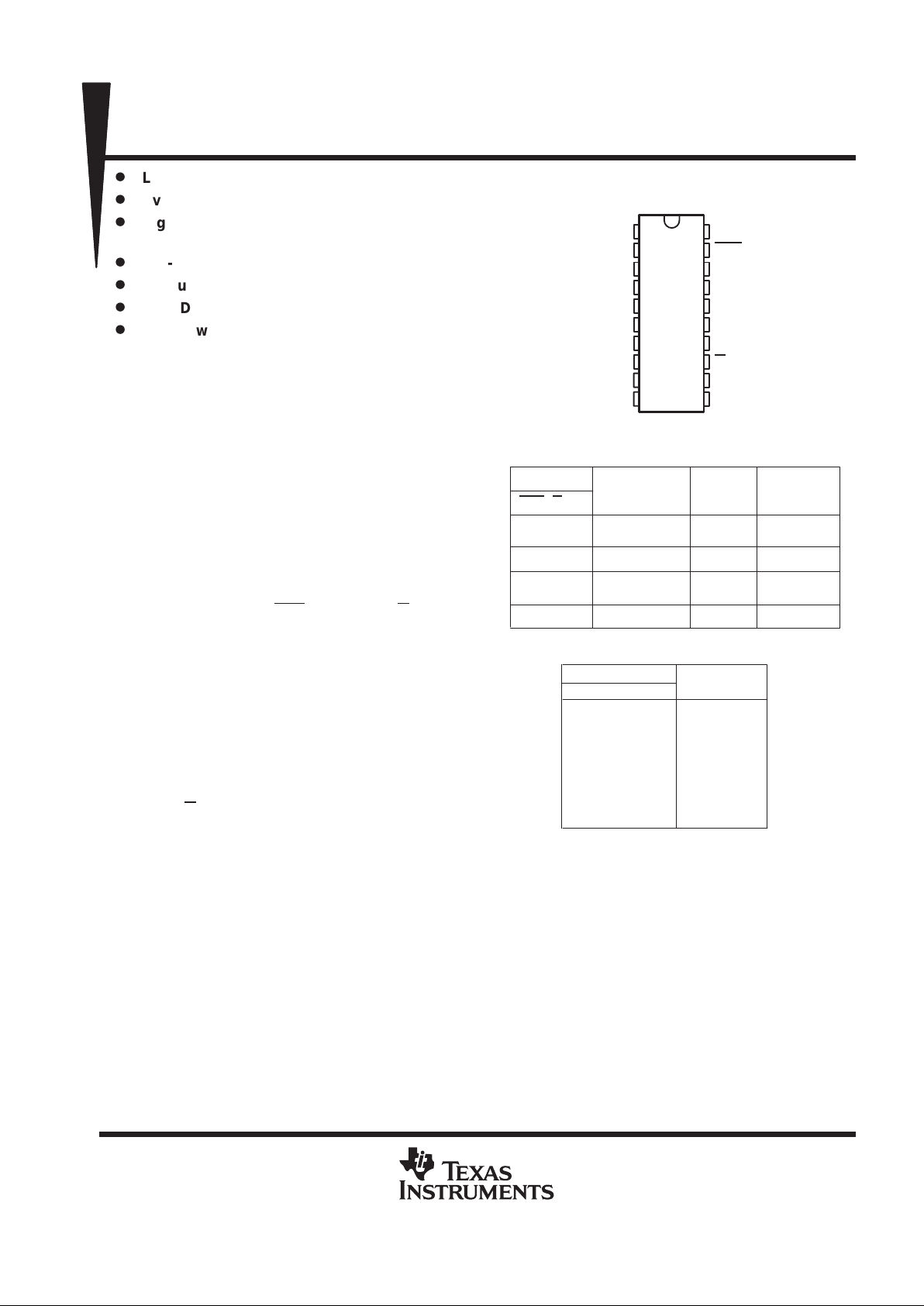
This power logic 8-bit addressable latch controls
open-drain DMOS-transistor outputs and is
designed for general-purpose storage
applications in digital systems. Specific uses
include working registers, serial-holding registers,
and decoders or demultiplexers. This is a multifunctional device capable of storing single-line
data in eight addressable latches and 3-to-8
decoder or demultiplexer with active-low DMOS
outputs.
Four distinct modes of operation are selectable by
controlling the clear (CLR
) and enable (G) inputs
as enumerated in the function table. In the
addressable-latch mode, data at the data-in (D)
terminal is written into the addressed latch. The
addressed DMOS-transistor output inverts the
data input with all unaddressed DMOS-transistor
outputs remaining in their previous states. In the
memory mode, all DMOS-transistor outputs
remain in their previous states and are unaffected
by the data or address inputs. To eliminate the
possibility of entering erroneous data in the latch,
enable G
should be held high (inactive) while the
address lines are changing. In the 3-to-8 decoding
or demultiplexing mode, the addressed output is
inverted with respect to the D input and all other
outputs are off. In the clear mode, all outputs are off and unaffected by the address and data inputs. When data
is low for a given output, the DMOS-transistor output is off. When data is high, the DMOS-transistor output has
sink-current capability .
Outputs are low-side, open-drain DMOS transistors with output ratings of 50 V and 150-mA continuous
sink-current capability. Each output provides a 500-mA typical current limit at TC = 25°C. The current limit
decreases as the junction temperature increases for additional device protection.
The TPIC6B259 is characterized for operation over the operating case temperature range of –40°C to 125°C.
Copyright 1997, Texas Instruments Incorporated
PRODUCTION DATA information is current as of publication date.
Products conform to specifications per the terms of Texas Instruments
standard warranty. Production processing does not necessarily include
testing of all parameters.
1
2
3
4
5
6
7
8
9
10
20
19
18
17
16
15
14
13
12
11
NC
V
CC
S0
DRAIN0
DRAIN1
DRAIN2
DRAIN3
S1
GND
GND
NC
CLR
D
DRAIN7
DRAIN6
DRAIN5
DRAIN4
G
S2
GND
DW OR N PACKAGE
(TOP VIEW)
OUTPUT OF
ADDRESSED
DRAIN
EACH
OTHER
DRAIN
INPUTS
FUNCTION
CLR G
FUNCTION TABLE
LATCH SELECTION TABLE
SELECT INPUTS DRAIN
ADDRESSED
0
1
2
3
4
5
6
7
L
L
L
L
H
H
H
H
D
HHLLH
L
L
H
Q
io
Q
io
Q
io
Q
io
H H X Memory
LLLLH
L
L
H
H
H
8-Line
Demultiplexer
L H X H H Clear
Addressable
Latch
S2 S1 S0
L
L
H
H
L
L
H
H
L
H
L
H
L
H
L
H
NC – No internal connection
H = high level, L = low level
PRODUCTION DATA information is current as of publication date.
Products conform to specifications per the terms of Texas Instruments
standard warranty. Production processing does not necessarily include
testing of all parameters.

TPIC6B259
POWER LOGIC 8-BIT ADDRESSABLE LATCH
SLIS030 – APRIL 1994 – REVISED JUL Y 1995
2
POST OFFICE BOX 655303 • DALLAS, TEXAS 75265
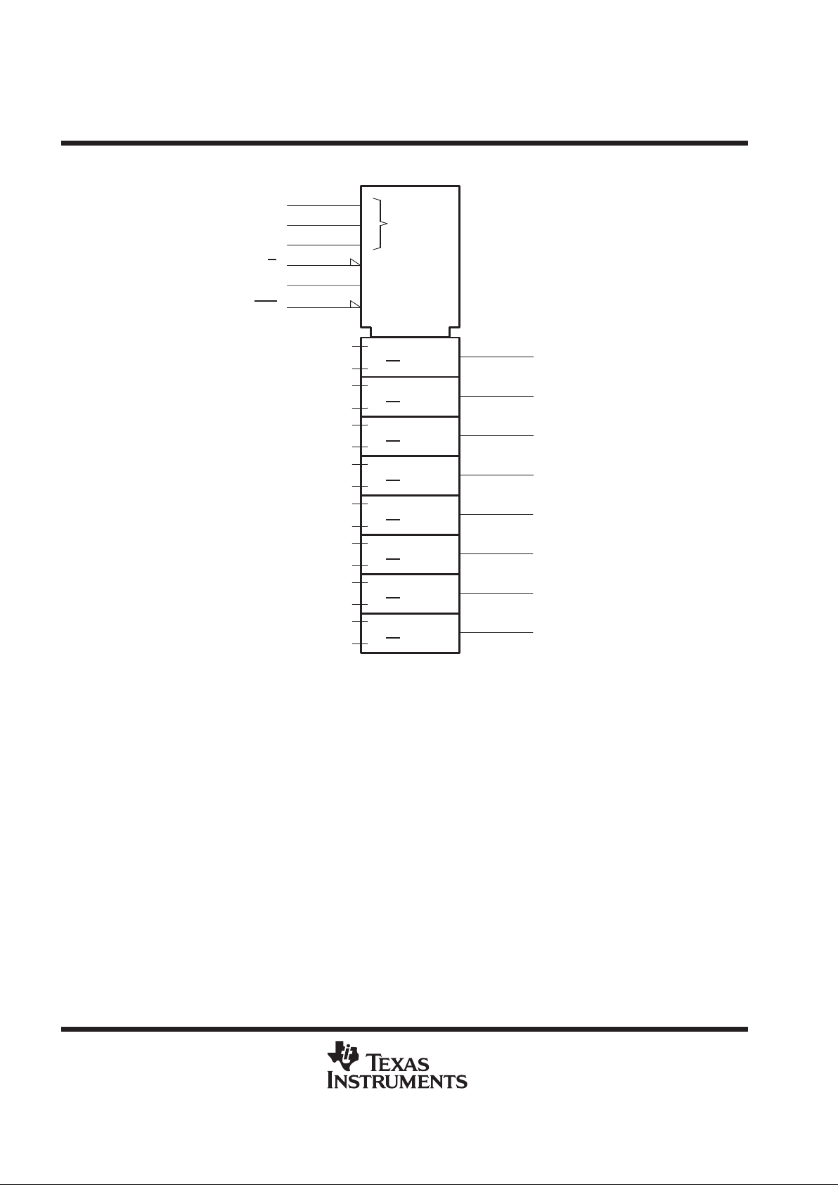
logic symbol
†
0
3
S0
8
S1
2
12
S2
G8
13
Z9
18
D
Z10
19
8M 0/7
9,0D
9,1D
9,2D
9,3D
9,4D
9,5D
9,6D
9,7D
10,0R
DRAIN0
4
DRAIN1
5
DRAIN2
6
DRAIN3
7
DRAIN4
14
DRAIN5
15
DRAIN6
16
DRAIN7
17
10,1R
10,2R
10,3R
10,4R
10,5R
10,6R
10,7R
G
CLR
†
This symbol is in accordance with ANSI/IEEE Std 91-1984 and IEC Publication 617-12.

TPIC6B259
POWER LOGIC 8-BIT ADDRESSABLE LATCH
SLIS030 – APRIL 1994 – REVISED JUL Y 1995
3
POST OFFICE BOX 655303 • DALLAS, TEXAS 75265
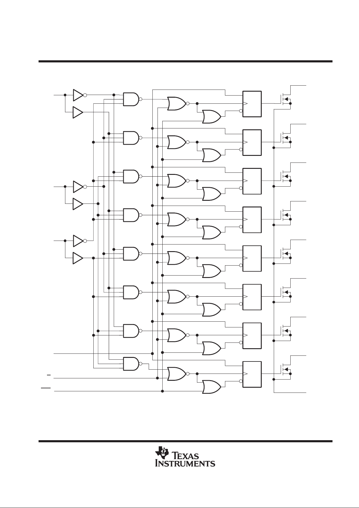
logic diagram (positive logic)
C1
S0
S2
S1
D
G
CLR
4
DRAIN0
5
DRAIN1
6
DRAIN2
7
DRAIN3
14
DRAIN4
15
DRAIN5
16
DRAIN6
17
DRAIN7
9,10,11
GND
3
12
8
18
13
19
D
CLR
C1
D
CLR
C1
D
CLR
C1
D
CLR
C1
D
CLR
C1
D
CLR
C1
D
CLR
C1
D
CLR

TPIC6B259
POWER LOGIC 8-BIT ADDRESSABLE LATCH
SLIS030 – APRIL 1994 – REVISED JUL Y 1995
4
POST OFFICE BOX 655303 • DALLAS, TEXAS 75265
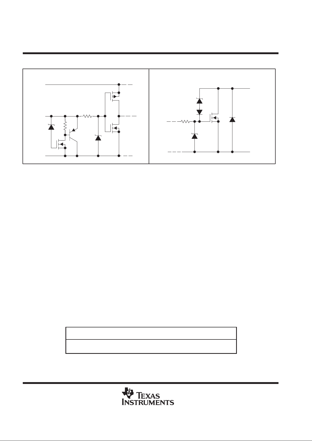
schematic of inputs and outputs
EQUIVALENT OF EACH INPUT TYPICAL OF ALL DRAIN OUTPUTS
V
CC
Input
GND
GND
DRAIN
50 V
20 V
25 V
12 V
absolute maximum ratings over the recommended operating case temperature range (unless
otherwise noted)
†
Logic supply voltage, VCC (see Note 1) 7 V. . . . . . . . . . . . . . . . . . . . . . . . . . . . . . . . . . . . . . . . . . . . . . . . . . . . . . .
Logic input voltage range, VI –0.3 V to 7 V. . . . . . . . . . . . . . . . . . . . . . . . . . . . . . . . . . . . . . . . . . . . . . . . . . . . . . . .
Power DMOS drain-to-source voltage, V
DS
(see Note 2) 50 V. . . . . . . . . . . . . . . . . . . . . . . . . . . . . . . . . . . . . . . .
Continuous source-to-drain diode anode current 500 mA. . . . . . . . . . . . . . . . . . . . . . . . . . . . . . . . . . . . . . . . . . . .
Pulsed source-to-drain diode anode current (see Note 3) 1 A. . . . . . . . . . . . . . . . . . . . . . . . . . . . . . . . . . . . . . . . .
Pulsed drain current, each output, all outputs on, ID, T
C
= 25°C (see Note 3) 500 mA. . . . . . . . . . . . . . . . . . .
Continuous drain current, each output, all outputs on, I
D
, T
C
= 25°C 150 mA. . . . . . . . . . . . . . . . . . . . . . . . . . .
Peak drain current single output, IDM, T
C
= 25°C (see Note 3) 500 mA. . . . . . . . . . . . . . . . . . . . . . . . . . . . . . . .
Single-pulse avalanche energy, EAS (see Figure 4) 30 mJ. . . . . . . . . . . . . . . . . . . . . . . . . . . . . . . . . . . . . . . . . . .
Avalanche current, IAS (see Note 4) 500 mA. . . . . . . . . . . . . . . . . . . . . . . . . . . . . . . . . . . . . . . . . . . . . . . . . . . . . .
Continuous total dissipation See Dissipating Rating Table. . . . . . . . . . . . . . . . . . . . . . . . . . . . . . . . . . . . . . . . . . .
Operating virtual junction temperature range, T
J
–40°C to 150°C. . . . . . . . . . . . . . . . . . . . . . . . . . . . . . . . . . . . .
Operating case temperature range, TC –40°C to 125°C. . . . . . . . . . . . . . . . . . . . . . . . . . . . . . . . . . . . . . . . . . . . .
Storage temperature range –65°C to 150°C. . . . . . . . . . . . . . . . . . . . . . . . . . . . . . . . . . . . . . . . . . . . . . . . . . . . . . . .
Lead temperature 1,6 mm (1/16 inch) from case for 10 seconds 260°C. . . . . . . . . . . . . . . . . . . . . . . . . . . . . . .
†
Stresses beyond those listed under “absolute maximum ratings” may cause permanent damage to the device. These are stress ratings only, and
functional operation of the device at these or any other conditions beyond those indicated under “recommended operating conditions” is not
implied. Exposure to absolute-maximum-rated conditions for extended periods may affect device reliability.
NOTES: 1. All voltage values are with respect to GND.
2. Each power DMOS source is internally connected to GND.
3. Pulse duration ≤ 100 µs and duty cycle ≤ 2%.
4. DRAIN supply voltage = 15 V , starting junction temperature (TJS) = 25°C, L = 200 mH, IAS = 0.5 A (see Figure 4).
DISSIPATION RATING TABLE
PACKAGE
TC ≤ 25°C
POWER RATING
DERATING FACTOR
ABOVE TC = 25°C
TC = 125°C
POWER RATING
DW 1389 mW 11.1 mW/°C 278 mW
N 1050 mW 10.5 mW/°C 263 mW
 Loading...