

TPIC6A595
POWER LOGIC 8-BIT SHIFT REGISTER
SLIS005A – APRIL 1993 – REVISED JANUARY 1995
1
POST OFFICE BOX 655303 • DALLAS, TEXAS 75265
D
Low r
DS(on)
...1 Ω Typ
D
Output Short-Circuit Protection
D
Avalanche Energy ...75 mJ
D
Eight 350-mA DMOS Outputs
D
50-V Switching Capability
D
Devices Are Cascadable
D
Low Power Consumption
description
The TPIC6A595 is a monolithic, high-voltage,
high-current power logic 8-bit shift register
designed for use in systems that require relatively
high load power. The device contains a built-in
voltage clamp on the outputs for inductive
transient protection. Power driver applications
include relays, solenoids, and other medium-current or high-voltage loads. Each open-drain
DMOS transistor features an independent
chopping current-limiting circuit to prevent
damage in the case of a short circuit.
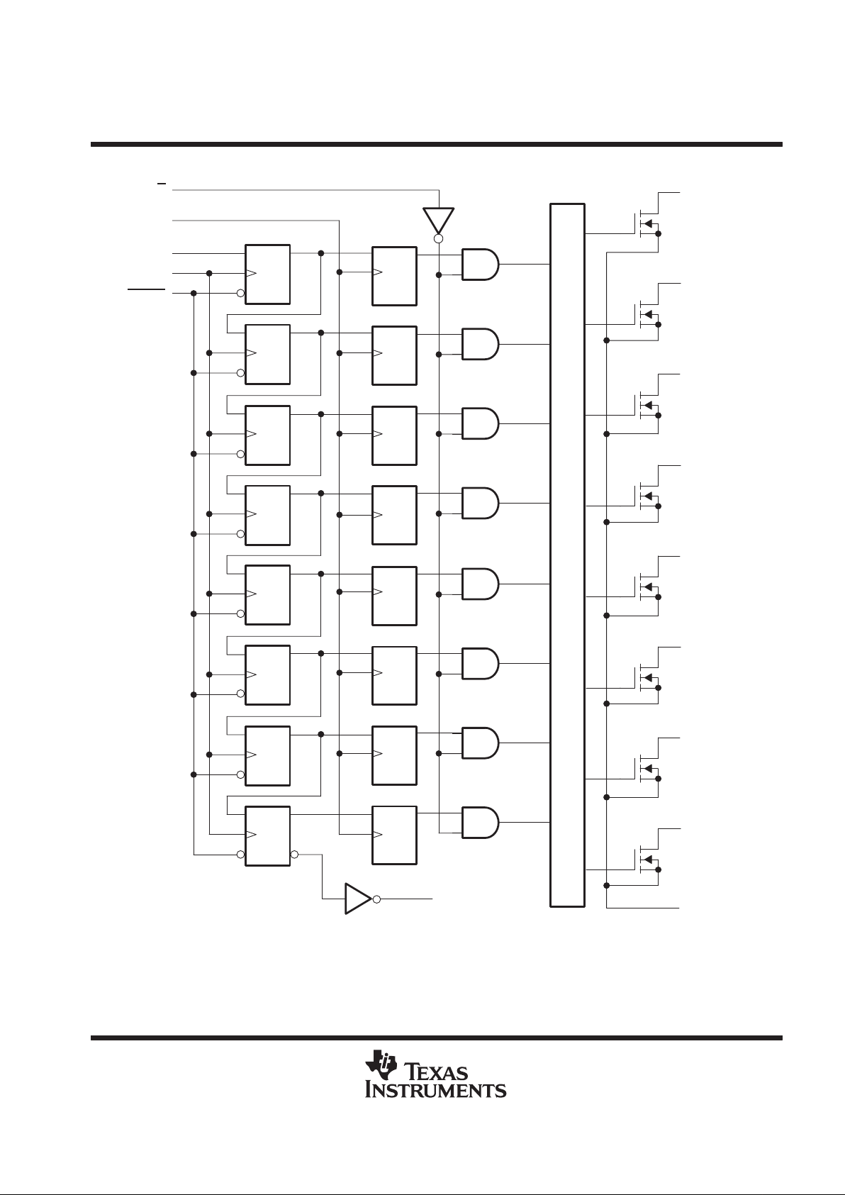
This device contains an 8-bit serial-in, parallel-out
shift register that feeds an 8-bit, D-type storage
register. Data transfers through both the shift and
storage registers on the rising edge of the shiftregister clock (SRCK) and the register clock
(RCK), respectively. The storage register
transfers data to the output buffer when shiftregister clear (SRCLR
) is high. When SRCLR is
low, the input shift register is cleared. When output
enable (G) is held high, all data in the output buffers is held low and all drain outputs are off. When G is held
low, data from the storage register is transparent to the output buf fers. The serial output (SER OUT) allows for
cascading of the data from the shift register to additional devices.
Outputs are low-side, open-drain DMOS transistors with output ratings of 50 V and a 350-mA continuous sink
current capability . When data in the output buffers is low, the DMOS-transistor outputs are off. When data is high,
the DMOS-transistor outputs have sink current capability.
Separate power ground (PGND) and logic ground (LGND) terminals are provided to facilitate maximum system
flexibility . All PGND terminals are internally connected, and each PGND terminal must be externally connected
to the power system ground in order to minimize parasitic impedance. A single-point connection between LGND
and PGND must be made externally in a manner that reduces crosstalk between the logic and load circuits.
The TPIC6A595 is offered in a thermally-enhanced dual-in-line (NE) package and a wide-body surface-mount
(DW) package. The TPIC6A595 is characterized for operation over the operating case temperature range of
–40°C to 125°C.
Copyright 1995, Texas Instruments Incorporated
PRODUCTION DATA information is current as of publication date.
Products conform to specifications per the terms of Texas Instruments
standard warranty. Production processing does not necessarily include
testing of all parameters.
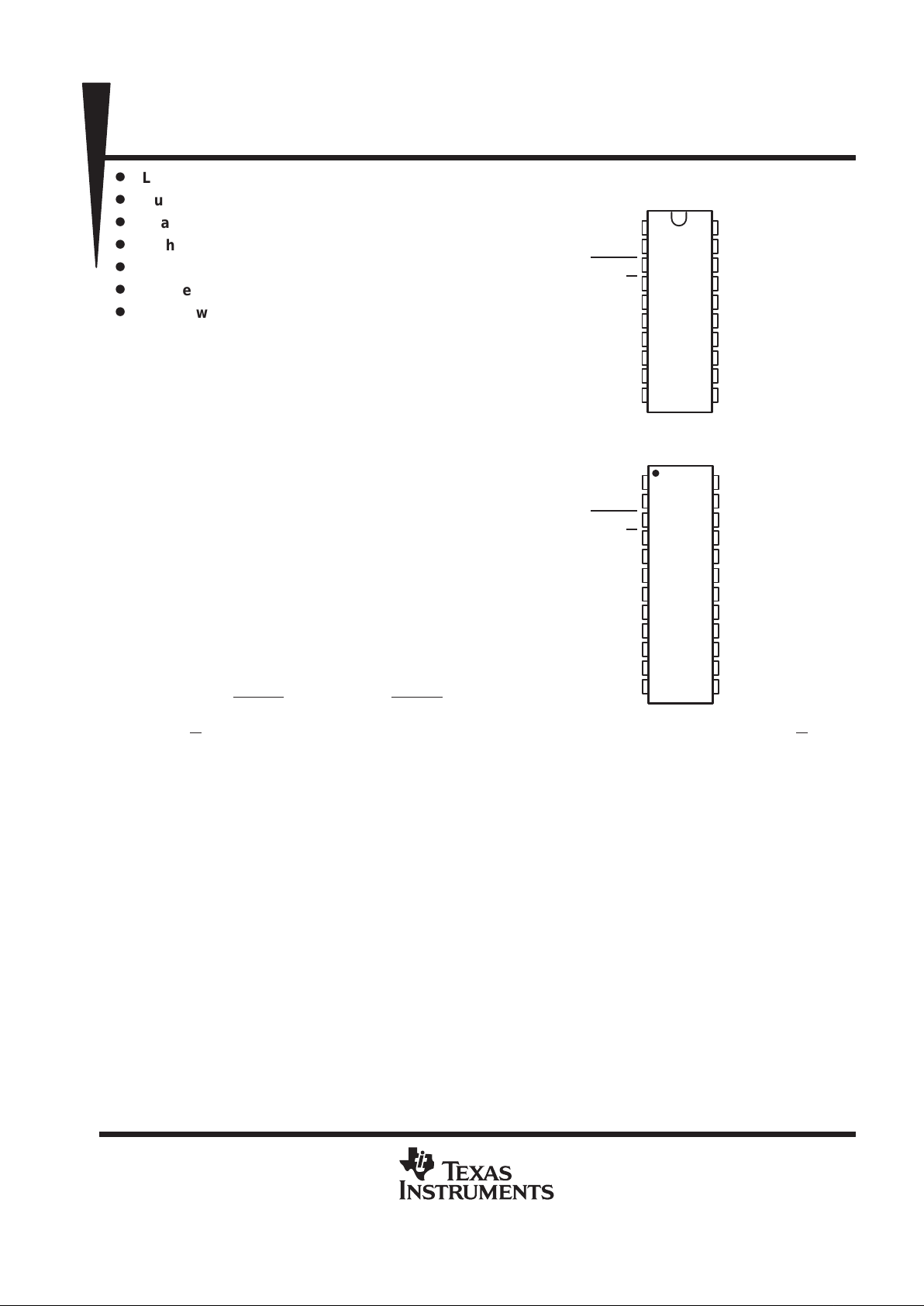
1
2
3
4
5
6
7
8
9
10
20
19
18
17
16
15
14
13
12
11
DRAIN2
DRAIN3
SRCLR
G
PGND
PGND
RCK
SRCK
DRAIN4
DRAIN5
DRAIN1
DRAN0
SER IN
V
CC
PGND
PGND
LGND
SER OUT
DRAIN7
DRAIN6
NE PACKAGE
(TOP VIEW)
1
2
3
4
5
6
7
8
9
10
11
12
24
23
22
21
20
19
18
17
16
15
14
13
DRAIN2
DRAIN3
SRCLR
G
PGND
PGND
PGND
PGND
RCK
SRCK
DRAIN4
DRAIN5
DRAIN1
DRAIN0
SER IN
V
CC
PGND
PGND
PGND
PGND
LGND
SER OUT
DRAIN7
DRAIN6
DW PACKAGE
(TOP VIEW)
TPIC6A595
POWER LOGIC 8-BIT SHIFT REGISTER
SLIS005A – APRIL 1993 – REVISED JANUARY 1995
2
POST OFFICE BOX 655303 • DALLAS, TEXAS 75265
logic symbol
†
SRG8
†
This symbol is in accordance with ANSI/IEEE Std 91-1984 and IEC Publication 617-12.
EN3
C2
R
C1
1D
G
RCK
SRCLR
SRCK
SER IN
DRAIN0
DRAIN1
DRAIN2
DRAIN3
DRAIN4
DRAIN5
DRAIN6
DRAIN7
SER OUT
2
2
3
3
TPIC6A595
POWER LOGIC 8-BIT SHIFT REGISTER
SLIS005A – APRIL 1993 – REVISED JANUARY 1995
3
POST OFFICE BOX 655303 • DALLAS, TEXAS 75265
logic diagram (positive logic)
G
RCK
SRCLR
SRCK
SER IN
CLR
D
C1
D
C2
CLR
D
C1
SER OUT
CLR
D
C1
CLR
D
C1
CLR
D
C1
CLR
D
C1
CLR
D
C1
CLR
D
C1
D
C2
D
C2
D
C2
D
C2
D
C2
D
C2
D
C2
DRAIN0
DRAIN1
DRAIN2
DRAIN3
DRAIN4
DRAIN5
DRAIN6
DRAIN7
Current Limit and Charge Pump
PGND
TPIC6A595
POWER LOGIC 8-BIT SHIFT REGISTER
SLIS005A – APRIL 1993 – REVISED JANUARY 1995
4
POST OFFICE BOX 655303 • DALLAS, TEXAS 75265
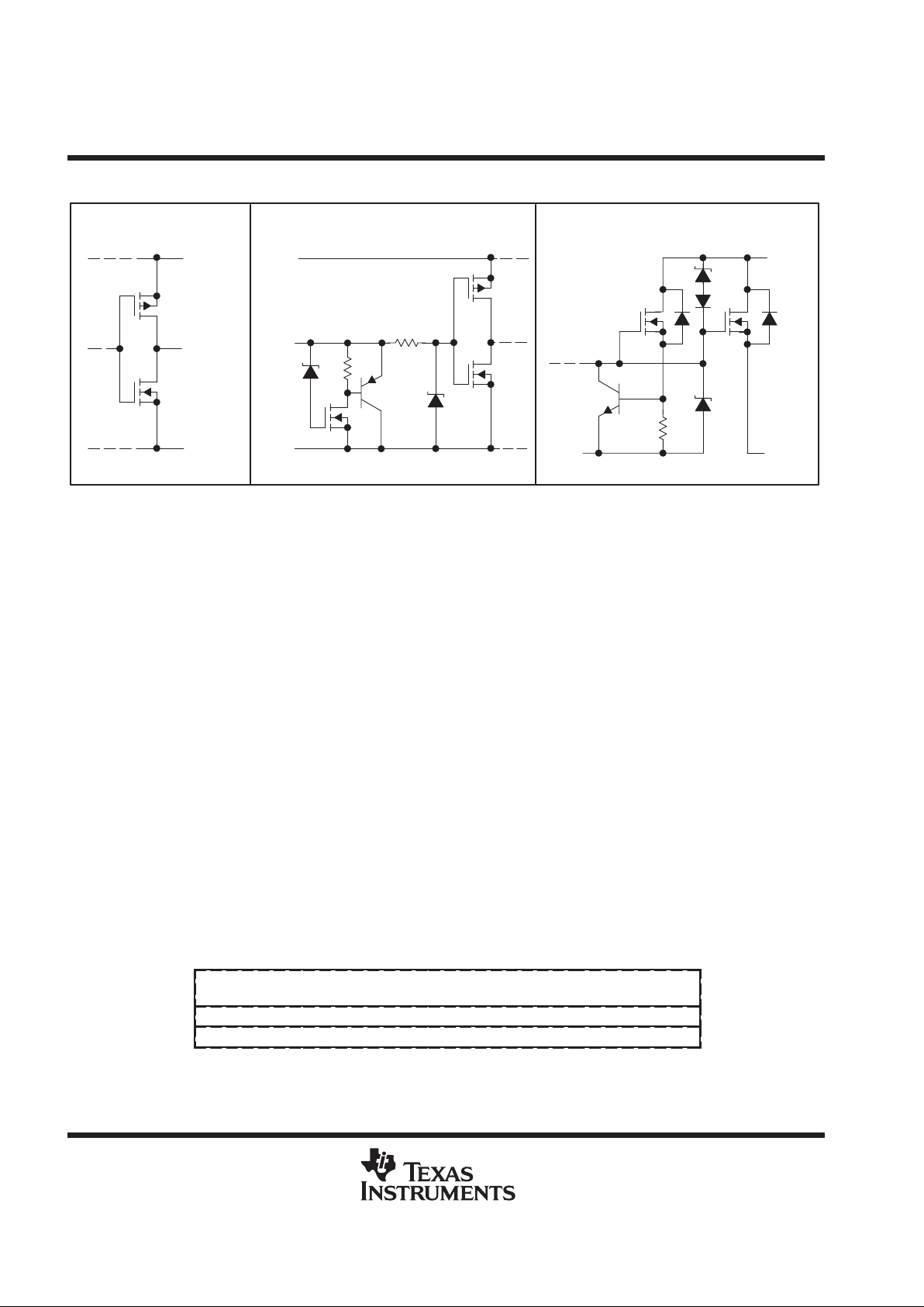
schematic of inputs and outputs
EQUIVALENT OF EACH INPUT TYPICAL OF ALL DRAIN OUTPUTS
V
CC
Input
LGND
PGND
DRAIN
25 V
12 V
LGND
R
SENSE
TYPICAL OF SERIAL OUT
V
CC
LGND
SER OUT
absolute maximum ratings over recommended operating case temperature range (unless
otherwise noted)
†
Logic supply voltage, VCC (see Note 1) 7 V. . . . . . . . . . . . . . . . . . . . . . . . . . . . . . . . . . . . . . . . . . . . . . . . . . . . . . .
Logic input voltage range, V
I
–0.3 V to 7 V. . . . . . . . . . . . . . . . . . . . . . . . . . . . . . . . . . . . . . . . . . . . . . . . . . . . . . . .
Power DMOS drain-to-source voltage, VDS (see Note 2) 50 V. . . . . . . . . . . . . . . . . . . . . . . . . . . . . . . . . . . . . . . .
Continuous source-drain diode anode current 1 A. . . . . . . . . . . . . . . . . . . . . . . . . . . . . . . . . . . . . . . . . . . . . . . . . .
Pulsed source-drain diode anode current (see Note 3) 2 A. . . . . . . . . . . . . . . . . . . . . . . . . . . . . . . . . . . . . . . . . . .
Pulsed drain current, each output, all outputs on, I
Dn,
T
A
= 25°C (see Note 3) 1.1 A. . . . . . . . . . . . . . . . . . . . .
Continuous drain current, each output, all outputs on, I
Dn,
TA = 25°C 350 mA. . . . . . . . . . . . . . . . . . . . . . . . . .
Peak drain current, single output, T
A
= 25°C (see Note 3) 1.1 A. . . . . . . . . . . . . . . . . . . . . . . . . . . . . . . . . . . . . .
Single-pulse avalanche energy, E
AS
(see Figure 6) 75 mJ. . . . . . . . . . . . . . . . . . . . . . . . . . . . . . . . . . . . . . . . . . .
Avalanche current, IAS (see Note 4) 600 mA. . . . . . . . . . . . . . . . . . . . . . . . . . . . . . . . . . . . . . . . . . . . . . . . . . . . . .
Continuous total dissipation See Dissipation Rating Table. . . . . . . . . . . . . . . . . . . . . . . . . . . . . . . . . . . . . . . . . . .
Operating case temperature range, TC –40°C to 125°C. . . . . . . . . . . . . . . . . . . . . . . . . . . . . . . . . . . . . . . . . . . . .
Operating virtual junction temperature range, TJ –40°C to 150°C. . . . . . . . . . . . . . . . . . . . . . . . . . . . . . . . . . . . .
Storage temperature range, T
stg
–65°C to 150°C. . . . . . . . . . . . . . . . . . . . . . . . . . . . . . . . . . . . . . . . . . . . . . . . . . .
Lead temperature 1,6 mm (1/16 inch) from case for 10 seconds 260°C. . . . . . . . . . . . . . . . . . . . . . . . . . . . . . .
†
Stresses beyond those listed under “absolute maximum ratings” may cause permanent damage to the device. These are stress ratings only, and
functional operation of the device at these or any other conditions beyond those indicated under “recommended operating conditions” is not
implied. Exposure to absolute-maximum-rated conditions for extended periods may affect device reliability.
NOTES: 1. All voltage values are with respect to LGND and PGND.
2. Each power DMOS source is internally connected to PGND.
3. Pulse duration ≤ 100 µs and duty cycle ≤ 2 %.
4. DRAIN supply voltage = 15 V, starting junction temperature (TJS) = 25°C, L = 210 mH, IAS = 600 mA (see Figure 6).
DISSIPATION RATING TABLE
PACKAGE
TC ≤ 25°C
POWER RATING
DERATING FACTOR
ABOVE TC = 25°C
TC = 125°C
POWER RATING
DW 1750 mW 14 mW/°C 350 mW
NE 2500 mW 20 mW/°C 500 mW

TPIC6A595
POWER LOGIC 8-BIT SHIFT REGISTER
SLIS005A – APRIL 1993 – REVISED JANUARY 1995
5
POST OFFICE BOX 655303 • DALLAS, TEXAS 75265
recommended operating conditions
MIN MAX UNIT
Logic supply voltage, V
CC
4.5 5.5 V
High-level input voltage, V
IH
0.85 V
CC
V
CC
V
Low-level input voltage, V
IL
0 0.15 V
CC
V
Pulsed drain output current, TC = 25°C, VCC = 5 V (see Notes 3 and 5) –1.8 0.6 A
Setup time, SER IN high before SRCK↑, tsu (see Figure 2) 10 ns
Hold time, SER IN high after SRCK↑, th (see Figure 2) 10 ns
Pulse duration, tw (see Figure 2) 20 ns
Operating case temperature, T
C
–40 125 °C
electrical characteristics, VCC = 5 V, TC = 25°C (unless otherwise noted)
PARAMETER TEST CONDITIONS MIN TYP MAX UNIT
V
(BR)DSX
Drain-to-source breakdown
voltage
ID = 1 mA 50 V
V
SD
Source-to-drain diode
forward voltage
IF = 350 mA, See Note 3 0.8 1.1 V
High-level output voltage,
IOH = –20 µA VCC–0.1 V
CC
V
OH
gg,
SER OUT
IOH = –4 mA
VCC–0.5 VCC–0.2
V
Low-level output voltage,
IOL = 20 µA 0 0.1
V
OL
g,
SER OUT
IOL = 4 mA
0.2 0.5
V
I
IH
High-level input current VI = V
CC
1 µA
I
IL
Low-level input current VI = 0 –1 µA
I
O(chop)
Output current at which
chopping starts
TC = 25°C,
See Note 5 and Figures 3 and 4
0.6 0.8 1.1 A
I
CC
Logic supply current IO = 0, VI = VCC or 0 0.5 5 mA
I
CC(FRQ)
Logic supply current at
frequency
f
SRCK
= 5 MHz, IO = 0, CL = 30 pF,
VI = VCC or 0, VCC = 5 V, See Figure 7
1.3 mA
I
(nom)
Nominal current
V
DS(on)
= 0.5 V, I
(nom)
= ID,TC = 85°C,
VCC = 5 V , See Notes 5, 6, and 7
350 mA
VDS = 40 V, TC = 25°C 0.1 1
IDDrain current, off-state
VDS = 40 V, TC = 125°C 0.2 5
µ
A
ID = 350 mA, TC = 25°C
1 1.5
r
DS(on
)
Static drai
n-source on-state
ID = 350 mA, TC = 125°C
S
ee Notes 5 and
6
1.7 2.5
Ω
(
resistance
ID = 350 mA, TC = 40°C
and Figures 10 and 11
NOTES: 3. Pulse duration ≤ 100 µs and duty cycle ≤ 2%.
5. Technique should limit TJ – TC to 10°C maximum.
6. These parameters are measured with voltage-sensing contacts separate from the current-carrying contacts.
7. Nominal current is defined for a consistent comparison between devices from different sources. It is the current that produces a
voltage drop of 0.5 V at TC = 85°C.

TPIC6A595
POWER LOGIC 8-BIT SHIFT REGISTER
SLIS005A – APRIL 1993 – REVISED JANUARY 1995
6
POST OFFICE BOX 655303 • DALLAS, TEXAS 75265
switching characteristics, VCC = 5 V, TC = 25°C
PARAMETER TEST CONDITIONS MIN TYP MAX UNIT
t
PHL
Propagation delay time, high-to-low-level output from G 30 ns
t
PLH
Propagation delay time, low-to-high-level output from G
C
= 30 pF, I
= 350 mA,
125 ns
t
r
Rise time, drain output
L
,
D
,
See Figures 1, 2, and 12
60 ns
t
f
Fall time, drain output 30 ns
t
a
Reverse-recovery-current rise time
IF = 350 mA, di/dt = 20 A/µs,
100 ns
t
rr
Reverse-recovery time
F
µ
See Notes 5 and 6 and Figure 5
300 ns
NOTES: 5. Technique should limit TJ – TC to 10°C maximum.
6. These parameters are measured with voltage-sensing contacts separate from the current-carrying contacts.
thermal resistance
PARAMETER TEST CONDITIONS MIN MAX UNIT
DW
p
p
10
°
R
θJC
Thermal resistance, junction-to-case
NE
All eight outputs with equal power
10
°C/W
DW
p
p
50
°
R
θJA
Thermal resistance, junction-to-ambient
NE
All eight outputs with equal power
50
°C/W

TPIC6A595
POWER LOGIC 8-BIT SHIFT REGISTER
SLIS005A – APRIL 1993 – REVISED JANUARY 1995
7
POST OFFICE BOX 655303 • DALLAS, TEXAS 75265
PARAMETER MEASUREMENT INFORMATION
TEST CIRCUIT
5 V
V
CC
DRAIN
LGND
SRCLR
SER IN
RL = 68 Ω
CL = 30 pF
(see Note B)
VOLTAGE WA VEFORMS
G
Output
SRCK
RCK
Word
Generator
(see Note A)
76543210
5 V
SRCK
5 V
G
5 V
SER IN
RCK
SRCLR
5 V
5 V
DUT
PGND
24 V
DRAIN 0, 1, 4, 5
24 V
0 V
0 V
0 V
0.5 V
0 V
0 V
I
D
24 V
DRAIN 2, 3, 6, 7
0.5 V
NOTES: A. The word generator has the following characteristics: tr ≤ 10 ns, tf ≤ 10 ns, tw = 300 ns, pulsed repetition rate (PRR) = 5 kHz,
ZO = 50 Ω.
B. CL includes probe and jig capacitance.
Figure 1. Resistive Load Operation
TEST CIRCUIT
SWITCHING TIMES
G
5 V
50%
24 V
0.5 V
90%
10%
t
PLH
t
r
50%
90%
10%
t
PHL
t
f
SRCK
5 V
50%
SER IN
5 V
50%
50%
t
su
t
h
t
w
INPUT SETUP AND HOLD WAVEFORMS
5 V 24 V
V
CC
DRAIN
LGND
SRCLR
SER IN
RL = 68 Ω
CL = 30 pF
(see Note B)
G
Output
SRCK
RCK
DUT
PGND
Output
Word
Generator
(see Note A)
0 V
0 V
0 V
I
D
NOTES: A. The word generator has the following characteristics: tr ≤ 10 ns, tf ≤ 10 ns, tw = 300 ns, pulsed repetition rate (PRR) = 5 kHz,
ZO = 50 Ω.
B. CL includes probe and jig capacitance.
Figure 2. Test Circuit, Switching Times, and Voltage Waveforms

TPIC6A595
POWER LOGIC 8-BIT SHIFT REGISTER
SLIS005A – APRIL 1993 – REVISED JANUARY 1995
8
POST OFFICE BOX 655303 • DALLAS, TEXAS 75265
PARAMETER MEASUREMENT INFORMATION
OUTPUT CURRENT
vs
TIME FOR INCREASING LOAD RESISTANCE
O
I – Output Current – A
I – Output Current
Region 1
Region 2
t
1
t
2
First output current pulses after turn-on in chopping mode with
resistive load.
0
1
1.5
O
0
t
1
≈ 40 µs
t2 ≈ 2.5 ms
Time
Time
I
OK
(see Notes A and B)
REGION 1 CURRENT WAVEFORM
I
OK
t
2
t
1
t
1
1.25
0.75
0.5
0.25
NOTES: A. Figure 3 illustrates the output current characteristics of the device energizing a load having initially low , increasing resistance, e.g.,
an incandescent lamp. In region 1, chopping occurs and the peak current is limited to IOK. In region 2, output current is continuous.
The same characteristics occur in reverse order when the device energizes a load having an initially high, decreasing resistance.
B. Region 1 duty cycle is approximately 2%.
Figure 3. Chopping-Mode Characteristics
0.9
0.6
0.3
0
– 50 – 25 0 25 50 75
1.2
OUTPUT CURRENT LIMIT
vs
CASE TEMPERATURE
100
TC – Case Temperature – °C
O
I – Output Current Limit – A
1.5
125 150
VCC = 5.5 V
VCC = 4.5 V
Figure 4

TPIC6A595
POWER LOGIC 8-BIT SHIFT REGISTER
SLIS005A – APRIL 1993 – REVISED JANUARY 1995
9
POST OFFICE BOX 655303 • DALLAS, TEXAS 75265
PARAMETER MEASUREMENT INFORMATION
+
–
2500 µF
250 V
L = 1 mH
I
F
(see Note B)
R
G
V
GG
(see Note A)
Driver
TP A
50 Ω
Circuit
Under
Test
DRAIN
24 V
t
1
t
3
t
2
TP K
TEST CIRCUIT
0.35 A
I
F
0
I
RM
(see Note C)
25% of I
RM
t
a
t
rr
di/dt = 20 A/µs
CURRENT WAVEFORM
NOTES: A. The VGG amplitude and RG are adjusted for di/dt = 20 A/µs. A VGG double-pulse train is used to set IF = 0.35 A, where t1 = 10 µs,
t2 = 7 µs, and t3 = 3 µs.
B. The DRAIN terminal under test is connected to the TP K test point. All other terminals are connected together and connected to the
TP A test point.
C. IRM = maximum recovery current
Figure 5. Reverse-Recovery-Current Test Circuit and Waveforms of Source-Drain Diode
15 V
1 Ω
210 mH
SINGLE-PULSE AVALANCHE ENERGY TEST CIRCUIT
t
w
t
av
†
IAS = 600 mA
V
(BR)DSX
= 50 V MIN
VOLTAGE AND CURRENT WAVEFORMS
Input
I
D
V
DS
See Note B
V
CC
DRAIN
LGND
SRCLR
SER IN
G
SRCK
RCK
Word
Generator
(see Note A)
DUT
PGND
5 V
V
DS
I
D
5 V
0 V
†
Non JEDEC symbol for avalanche time.
NOTES: A. The word generator has the following characteristics: tr ≤ 10 ns, tf ≤ 10 ns, ZO = 50 Ω.
B. Input pulse duration, tw, is increased until peak current IAS = 600 mA.
Energy test level is defined as EAS = (IAS × V
(BR)DSX
× tav)/2 = 75 mJ.
Figure 6. Single-Pulse Avalanche Energy Test Circuit and Waveforms

TPIC6A595
POWER LOGIC 8-BIT SHIFT REGISTER
SLIS005A – APRIL 1993 – REVISED JANUARY 1995
10
POST OFFICE BOX 655303 • DALLAS, TEXAS 75265
TYPICAL CHARACTERISTICS
Figure 7
I – Supply Current – mA
CC
SUPPLY CURRENT
vs
FREQUENCY
f – Frequency – MHz
1
0.5
0
0.1 1 10
1.5
2
100
2.5
3
3.5
4
VCC = 5 V
TJS = –40°C to 125°C
Figure 8
– Maximum Continuous Drain Current
MAXIMUM CONTINUOUS
DRAIN CURRENT OF EACH OUTPUT
vs
NUMBER OF OUTPUTS CONDUCTING
SIMULTANEOUSLY
0.4
0.2
0.1
0
12345
0.6
0.7
678
0.5
0.3
VCC = 5 V
TA = 25°C
TA = 100°C
TA = 125°C
N – Number of Outputs Conducting Simultaneously
of Each Output – A
D
I
Figure 9
– Maximum Peak Drain Current of Each Output – A
DM
N – Number of Outputs Conducting Simultaneously
I
0.2
0.1
0
12345 678
0.3
d = 20%d = 50%
d = 80%
0.4
0.7
0.6
0.5
0.8
0.9
VCC = 5 V
TA = 25°C
d = tw/t
period
d = 1 ms/t
period
MAXIMUM PEAK DRAIN CURRENT
OF EACH OUTPUT
vs
NUMBER OF OUTPUTS CONDUCTING
SIMULTANEOUSLY
Figure 10
STATIC DRAIN-SOURCE ON-STATE RESISTANCE
vs
DRAIN CURRENT
NOTE A: Technique should limit TJ – TC to 10°C maximum.
ID – Drain Current – A
Ω
DS(on)
– Static Drain-Source On-State Resistance –r
1
0.75
0.25
0
0 0.2 0.4 0.6
1.25
1.75
2
0.8 1
0.5
1.5
TC = 25°C
TC = 125°C
TC = – 40°C
1.2
VCC = 5 V
See Note A
Current Limit

TPIC6A595
POWER LOGIC 8-BIT SHIFT REGISTER
SLIS005A – APRIL 1993 – REVISED JANUARY 1995
11
POST OFFICE BOX 655303 • DALLAS, TEXAS 75265
TYPICAL CHARACTERISTICS
Figure 11
VCC – Logic Supply Voltage – V
0
0.25
0.5
0.75
1
1.25
1.5
45 67
TC = 125°C
STATIC DRAIN-SOURCE ON-STATE RESISTANCE
vs
LOGIC SUPPLY VOLTAGE
Ω
DS(on)
– Static Drain-Source On-State Resistance –r
TC = 25°C
TC = –40°C
1.75
2
ID = 350 mA
See Note A
Figure 12
100
60
40
20
140
80
– 50 0 50 100 150
120
SWITCHING TIME
vs
CASE TEMPERATURE
Switching Time – ns
t
PLH
t
r
t
f
TC – Case Temperature – °C
t
PHL
ID = 350 mA
See Note A
NOTE A: Technique should limit TJ – TC to 10°C maximum.
THERMAL INFORMATION
NE PACKAGE
TRANSIENT THERMAL IMPEDANCE
vs
ON TIME
The single-pulse curve represents measured data. The
curves for various pulse durations are based on the
following equation:
t – On Time – s
C
°
θ
Z – Transient Thermal Impedance – /W
JA
0.1
0.001 0.01 0.1 1 10 100
1
10
100
1000
Single Pulse
d = 2%
d = 5%
d = 10%
d = 20%
d = 50%
t
w
t
c
I
D
0
Z
q
JA
+
Ť
t
w
t
c
Ť
R
q
JA
)
Ť
1 –
t
w
t
c
Ť
Z
q
ǒ
tw)
t
c
Ǔ
)
Z
q
ǒ
t
w
Ǔ
–Z
q
ǒ
t
c
Ǔ
= the single-pulse thermal impedance
for t = tw seconds
= the single-pulse thermal impedance
for t = tc seconds
= the single-pulse thermal impedance
for t = tw + tc seconds
Where:
d = tw/t
c
Z
q
ǒ
t
w
Ǔ
Z
q
ǒ
t
c
Ǔ
Z
q
ǒ
tw)
t
c
Ǔ
Figure 13

IMPORTANT NOTICE
T exas Instruments and its subsidiaries (TI) reserve the right to make changes to their products or to discontinue
any product or service without notice, and advise customers to obtain the latest version of relevant information
to verify, before placing orders, that information being relied on is current and complete. All products are sold
subject to the terms and conditions of sale supplied at the time of order acknowledgement, including those
pertaining to warranty, patent infringement, and limitation of liability.
TI warrants performance of its semiconductor products to the specifications applicable at the time of sale in
accordance with TI’s standard warranty. Testing and other quality control techniques are utilized to the extent
TI deems necessary to support this warranty. Specific testing of all parameters of each device is not necessarily
performed, except those mandated by government requirements.
CERT AIN APPLICATIONS USING SEMICONDUCT OR PRODUCTS MAY INVOLVE POTENTIAL RISKS OF
DEATH, PERSONAL INJURY, OR SEVERE PROPERTY OR ENVIRONMENTAL DAMAGE (“CRITICAL
APPLICATIONS”). TI SEMICONDUCTOR PRODUCTS ARE NOT DESIGNED, AUTHORIZED, OR
WARRANTED TO BE SUITABLE FOR USE IN LIFE-SUPPORT DEVICES OR SYSTEMS OR OTHER
CRITICAL APPLICATIONS. INCLUSION OF TI PRODUCTS IN SUCH APPLICA TIONS IS UNDERSTOOD T O
BE FULLY AT THE CUSTOMER’S RISK.
In order to minimize risks associated with the customer’s applications, adequate design and operating
safeguards must be provided by the customer to minimize inherent or procedural hazards.
TI assumes no liability for applications assistance or customer product design. TI does not warrant or represent
that any license, either express or implied, is granted under any patent right, copyright, mask work right, or other
intellectual property right of TI covering or relating to any combination, machine, or process in which such
semiconductor products or services might be or are used. TI’s publication of information regarding any third
party’s products or services does not constitute TI’s approval, warranty or endorsement thereof.
Copyright 2000, Texas Instruments Incorporated
 Loading...