

Page 1
TPIC2701
7-CHANNEL COMMON-SOURCE POWER DMOS ARRAY
SLIS019A – SEPTEMBER 1992 – REVISED SEPTEMBER 1996
1
POST OFFICE BOX 655303 • DALLAS, TEXAS 75265
D
Seven 0.5-A Independent Output Channels
D
Integrated Clamp Diode With Each Output
D
Low r
DS(on)
. . . 0.5 Ω Typical
D
Output Voltage . . . 60 V
D
Pulsed Current...3 A Per Channel
D
Avalanche Energy...22 mJ
description
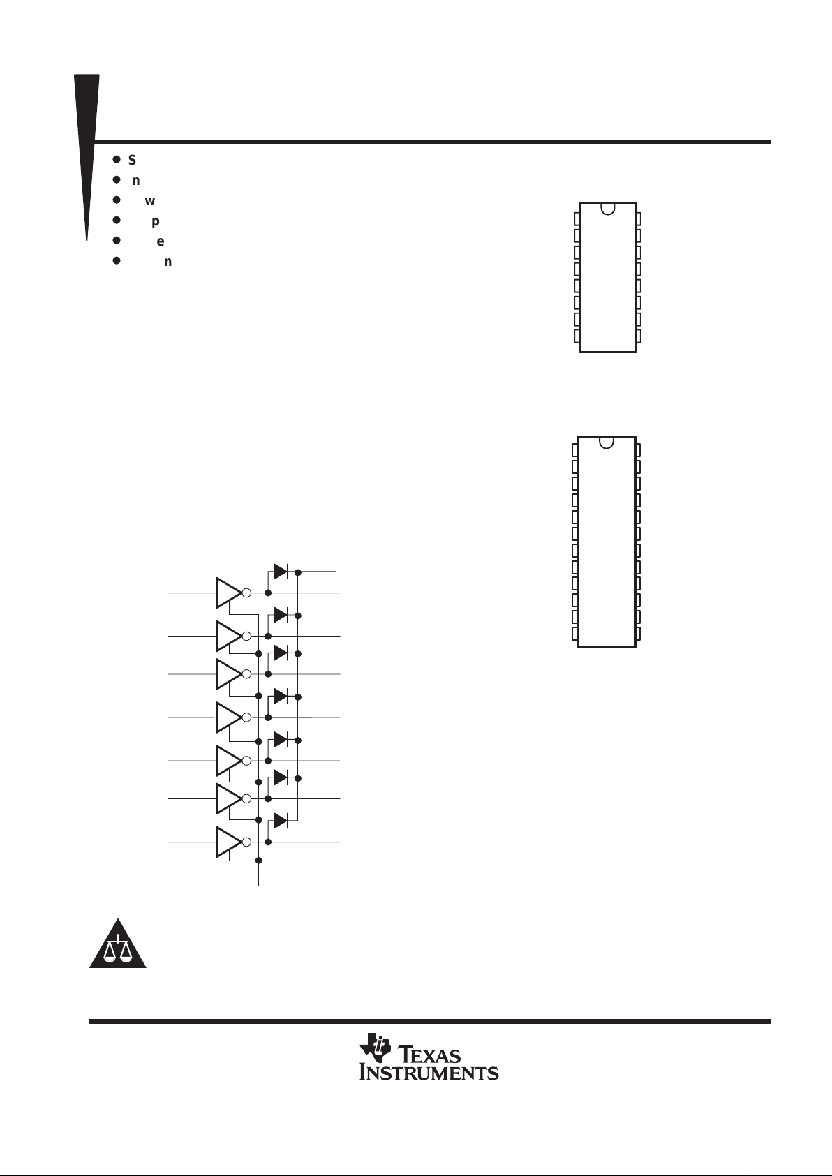
The TPIC2701 is a monolithic power DMOS
transistor array that consists of seven independent N-channel enhancement-mode DMOS
transistors connected in a common-source
configuration with open drains. The TPIC2701 is
pin-for-pin functionally compatible with the Texas
Instruments ULN2001A through ULN2004A.
The TPIC2701 is characterized for operation over
a temperature range of 0°C to 125°C.The
TPIC2701M is characterized for operation over
the full military temperature range of – 55°C to
125°C.
logic diagram
CLAMP
DRAIN1
DRAIN2
DRAIN3
DRAIN4
DRAIN5
DRAIN6
DRAIN7
GATE1
GATE2
GATE3
GATE4
GATE5
GATE6
GATE7
1
2
3
4
5
6
7
SOURCE
8
9
16
15
14
13
12
11
10
Please be aware that an important notice concerning availability, standard warranty, and use in critical applications of
Texas Instruments semiconductor products and disclaimers thereto appears at the end of this data sheet.
Copyright 1996, Texas Instruments Incorporated
PRODUCTION DATA information is current as of publication date.
Products conform to specifications per the terms of Texas Instruments
standard warranty. Production processing does not necessarily include
testing of all parameters.
1
2
3
4
5
6
7
8
16
15
14
13
12
11
10
9
GATE1
GATE2
GATE3
GATE4
GATE5
GATE6
GATE7
SOURCE
DRAIN1
DRAIN2
DRAIN3
DRAIN4
DRAIN5
DRAIN6
DRAIN7
CLAMP
1
2
3
4
5
6
7
8
9
10
11
12
24
23
22
21
20
19
18
17
16
15
14
13
GATE1
GATE2
GATE3
NC
NC
GATE4
GATE5
NC
GATE6
GATE7
SOURCE
SOURCE
DRAIN1
DRAIN2
DRAIN3
NC
NC
DRAIN4
DRAIN5
NC
DRAIN6
DRAIN7
CLAMP
SOURCE
TPIC2701M
J PACKAGE
†
(TOP VIEW)
NC – No internal connection
TPIC2701
N PACKAGE
(TOP VIEW)
†
Refer to the mechanical data for the JW package.
Page 2
TPIC2701
7-CHANNEL COMMON-SOURCE POWER DMOS ARRAY
SLIS019A – SEPTEMBER 1992 – REVISED SEPTEMBER 1996
2
POST OFFICE BOX 655303 • DALLAS, TEXAS 75265
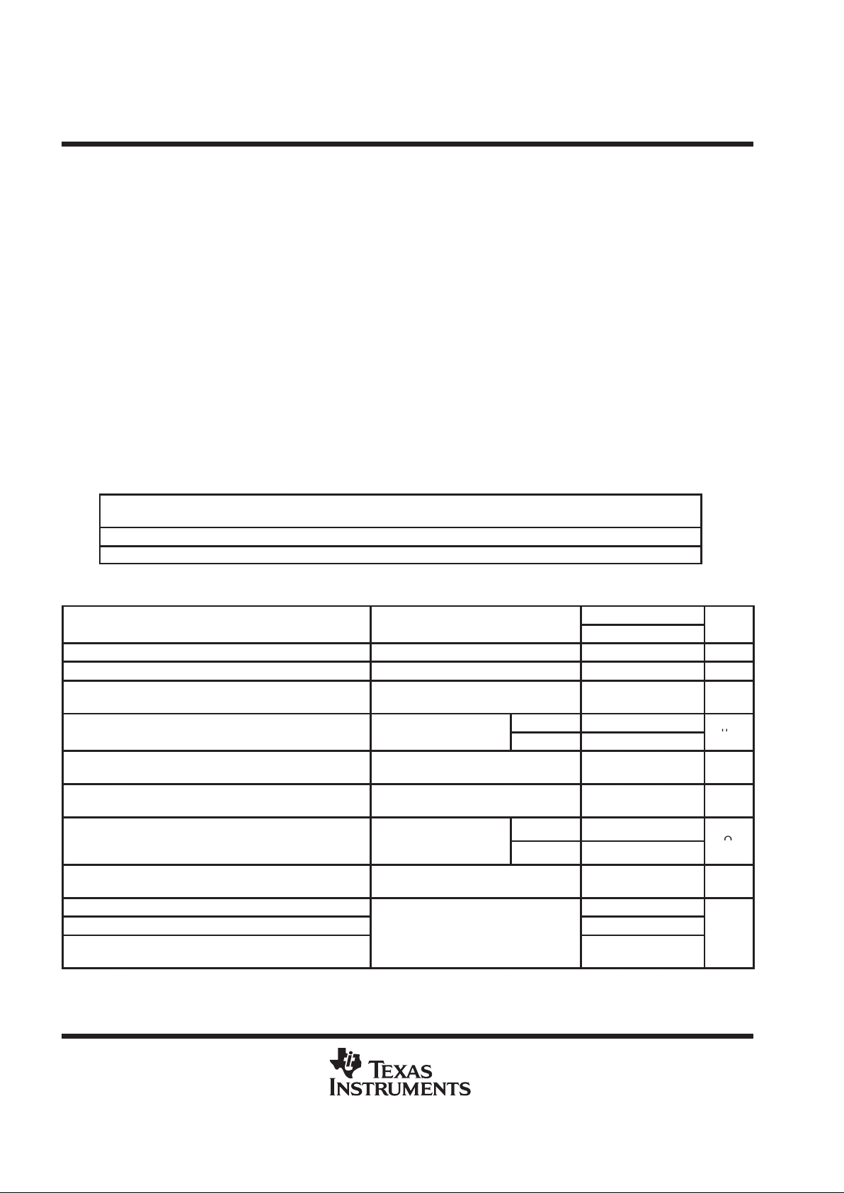
absolute maximum ratings over operating case temperature range (unless otherwise noted)
Drain-source voltage, VDS 60 V. . . . . . . . . . . . . . . . . . . . . . . . . . . . . . . . . . . . . . . . . . . . . . . . . . . . . . . . . . . . . . . . .
Gate-source voltage, V
GS
±20 V. . . . . . . . . . . . . . . . . . . . . . . . . . . . . . . . . . . . . . . . . . . . . . . . . . . . . . . . . . . . . . . . . .
Clamp-drain voltage, V
CD
60 V. . . . . . . . . . . . . . . . . . . . . . . . . . . . . . . . . . . . . . . . . . . . . . . . . . . . . . . . . . . . . . . . . . .
Continuous source-drain diode current 0.5 A. . . . . . . . . . . . . . . . . . . . . . . . . . . . . . . . . . . . . . . . . . . . . . . . . . . . . .
Pulsed drain current, each output, I
D
(see Note 1 and Figure 17) 3 A. . . . . . . . . . . . . . . . . . . . . . . . . . . . . . . . . .
Pulsed clamp current, I
CL
(see Note 1 and Figure 18) 3 A. . . . . . . . . . . . . . . . . . . . . . . . . . . . . . . . . . . . . . . . . . .
Continuous drain current, each output, all outputs on 0.5 A. . . . . . . . . . . . . . . . . . . . . . . . . . . . . . . . . . . . . . . . . .
Single-pulse avalanche energy, E
AS
(see Figure 4) 22 mJ. . . . . . . . . . . . . . . . . . . . . . . . . . . . . . . . . . . . . . . . . . . .
Continuous total power dissipation See Dissipation Rating Table. . . . . . . . . . . . . . . . . . . . . . . . . . . . . . . . . . . . .
Operating virtual junction temperature range, T
J
:TPIC2701 –40°C to 150°C. . . . . . . . . . . . . . . . . . . . . . . . . . .
TPIC2701M –55°C to 150°C. . . . . . . . . . . . . . . . . . . . . . . . . .
Operating case temperature range, T
C:
TPIC2701 –40°C to 125°C. . . . . . . . . . . . . . . . . . . . . . . . . . . . . . . . . . .
TPIC2701M –55°C to 125°C. . . . . . . . . . . . . . . . . . . . . . . . . . . . . . . . .
Storage temperature range, T
stg
–65°C to 150°C. . . . . . . . . . . . . . . . . . . . . . . . . . . . . . . . . . . . . . . . . . . . . . . . . . .
Lead temperature 1,6 mm (1/16 inch) from case for 10 seconds: N Package 260°C. . . . . . . . . . . . . . . . . . . . .
Lead temperature 1,6 mm (1/16 inch) from case for 10 seconds: J Package 300°C. . . . . . . . . . . . . . . . . . . . .
NOTE 1: Pulse duration = 10 ms, duty cycle = 6%.
DISSIPATION RATING TABLE
PACKAGE
TA ≤ 25°C
POWER RATING
DERATING FACTOR
ABOVE TA = 25°C
TA = 70°C
POWER RATING
TA = 85°C
POWER RATING
TA = 125°C
POWER RATING
J 2660 mW 21.3 mW/°C 1701 mW 1382 mW 530 mW
N 1400 mW 11.0 mW/°C 905 mW 740 mW 300 mW
electrical characteristics, TC = 25°C (unless otherwise noted)
TPIC2701
PARAMETER
TEST CONDITIONS
MIN TYP MAX
UNIT
V
(BR)DS
Drain-source breakdown voltage ID = 1 µA, VGS = 0 60 V
V
TGS
Gate-source threshold voltage ID = 1 mA, VDS = V
GS
1.2 1.75 2.4 V
V
DS(on)
Drain-source on-state voltage
ID = 0.5 A, VGS = 15 V,
See Notes 2 and 3
0.25 0.4 V
TC = 25°C 0.05 1
I
DSS
Zero-gate-voltage drain current
V
DS
= 48 V,
V
GS
=
0
TC = 125°C 0.5 10
µ
A
I
GSSF
Forward gate current, drain short circuited to
source
VGS = 20 V, VDS = 0 10 100 nA
I
GSSR
Reverse gate current, drain short circuited to
source
VGS = –20 V , VDS = 0 10 100 nA
VGS = 15 V, ID = 0.5 A,
TC = 25°C 0.5 0.8
r
DS(on)
Forward drain-source on-state resistance
S
ee Notes 2 and 3 an
d
Figures 5 and 6
TC = 125°C 0.8 1.3
Ω
g
fs
Forward transconductance
VDS = 15 V, ID = 0.5 A,
See Notes 2 and 3
0.5 0.8 S
C
iss
Short-circuit input capacitance, common source 105
C
oss
Short-circuit output capacitance, common source
65
p
C
rss
Short-circuit reverse transfer capacitance,
common source
V
DS
= 25 V,
V
GS
= 0,f =
300 kHz
15
F
NOTES: 2. Technique should limit TJ – TC to 10°C maximum.
3. These parameters are measured with voltage-sensing contacts separate from the current-carrying contacts with a single output
transistor conducting.
Page 3
TPIC2701
7-CHANNEL COMMON-SOURCE POWER DMOS ARRAY
SLIS019A – SEPTEMBER 1992 – REVISED SEPTEMBER 1996
3
POST OFFICE BOX 655303 • DALLAS, TEXAS 75265
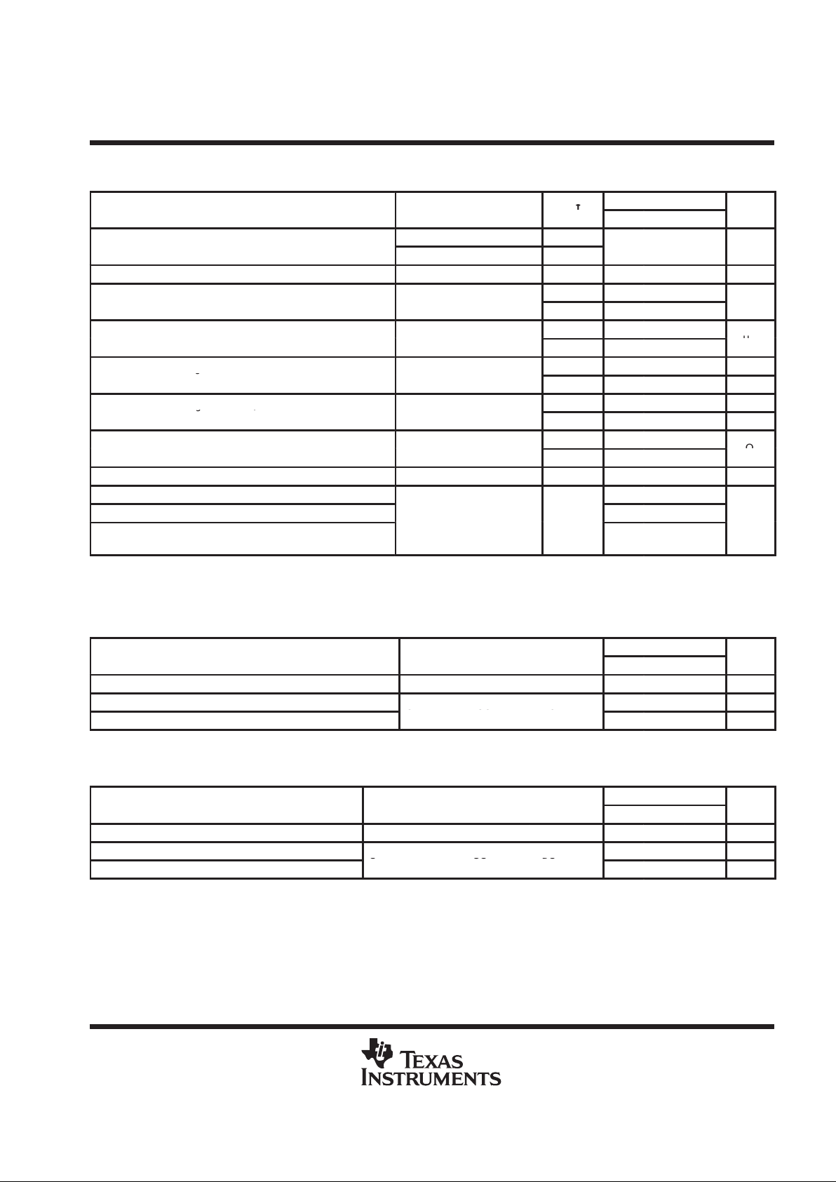
electrical characteristics over case temperature operating range (unless otherwise noted)
(see Note 4)
TPIC2701M
PARAMETER
TEST CONDITIONS
T
C
†
MIN TYP MAX
UNIT
ID = 1 µA, VGS = 0 25°C
V
(BR)DS
Drain-to-source breakdown voltage
ID = 1 mA, VGS = 0 Full range
60
V
V
TGS
Gate-to-source input threshold voltage ID = 1 mA, VDS = V
GS
Full range 1.2 1.75 2.4 V
25°C 0.25 0.45
V
DS(on)
Drain-to-source on-state voltage
I
D
=
0.5 A
,
V
GS
=
15 V
Full range 0.65
V
25°C 0.05 1
I
DSS
Zero-gate-voltage drain current
V
DS
= 48 V,
V
GS
=
0
Full range 10
µ
A
Forward gate current, drain short-circuited to
25°C 10 100 nA
I
GSSF
g,
source
V
GS
= 20 V,
V
DS
=
0
Full range 10 µA
Reverse gate current, drain short-circuited to
25°C 10 100 nA
I
GSSR
g,
source
V
GS
= –
20 V,V
DS
=
0
Full range 10 µA
25°C 0.5 0.9
r
DS(on)
Forward drain-source on-state resistance
V
GS
= 15 V,
I
D
= 0.5
A
Full range 1.3
Ω
g
fs
Forward transconductance VDS = 15 V, ID = 0.5 A 25°C 0.8 S
C
iss
Short-circuit input capacitance, common source 105
C
oss
Short-circuit output capacitance, common source
VDS = 25 V, VGS = 0,
65
p
C
rss
Short-circuit reverse transfer capacitance,
common source
f = 300 kHz
Full range
15
F
†
Full range is –55°C to 125°C.
NOTE 4: Pulse testing techniques are used to maintain the virtual junction temperature as close to the case temperature as possible. Thermal
effects must be taken into account separately.
source-drain diode characteristics, TC = 25°C
TPIC2701
PARAMETER
TEST CONDITIONS
MIN TYP MAX
UNIT
V
SD
Forward On voltage IS = 0.5 A, VGS = 0 0.9 1.4 V
t
rr(SD)
Reverse-recovery time
IS = 0.5 A, VGS = 0, VDS = 48 V,
165 ns
Q
RR
Total source-drain diode charge
SGS
di/dt = 25 A/µs,
DS
See Figure 1
250 nC
source-to-drain diode characteristics over operating case temperature range (unless otherwise
noted) (see Note 4)
TPIC2701M
PARAMETER
TEST CONDITIONS
MIN TYP MAX
UNIT
V
SD
Forward On voltage IS = 0.5 A, VGS = 0 0.9 1.4 V
t
rr
Reverse recovery time
IS = 0.5 A, VGS = 0, VDS = 48 V,
165 ns
Q
RR
Total source-to-drain diode charge
SGS
di/dt = 25 A/µs, TC = 25°C,DSSee Figure 1
250 nC
NOTE 4: Pulse testing techniques are used to maintain the virtual junction temperature as close to the case temperature as possible. Thermal
effects must be taken into account separately.
Page 4
TPIC2701
7-CHANNEL COMMON-SOURCE POWER DMOS ARRAY
SLIS019A – SEPTEMBER 1992 – REVISED SEPTEMBER 1996
4
POST OFFICE BOX 655303 • DALLAS, TEXAS 75265
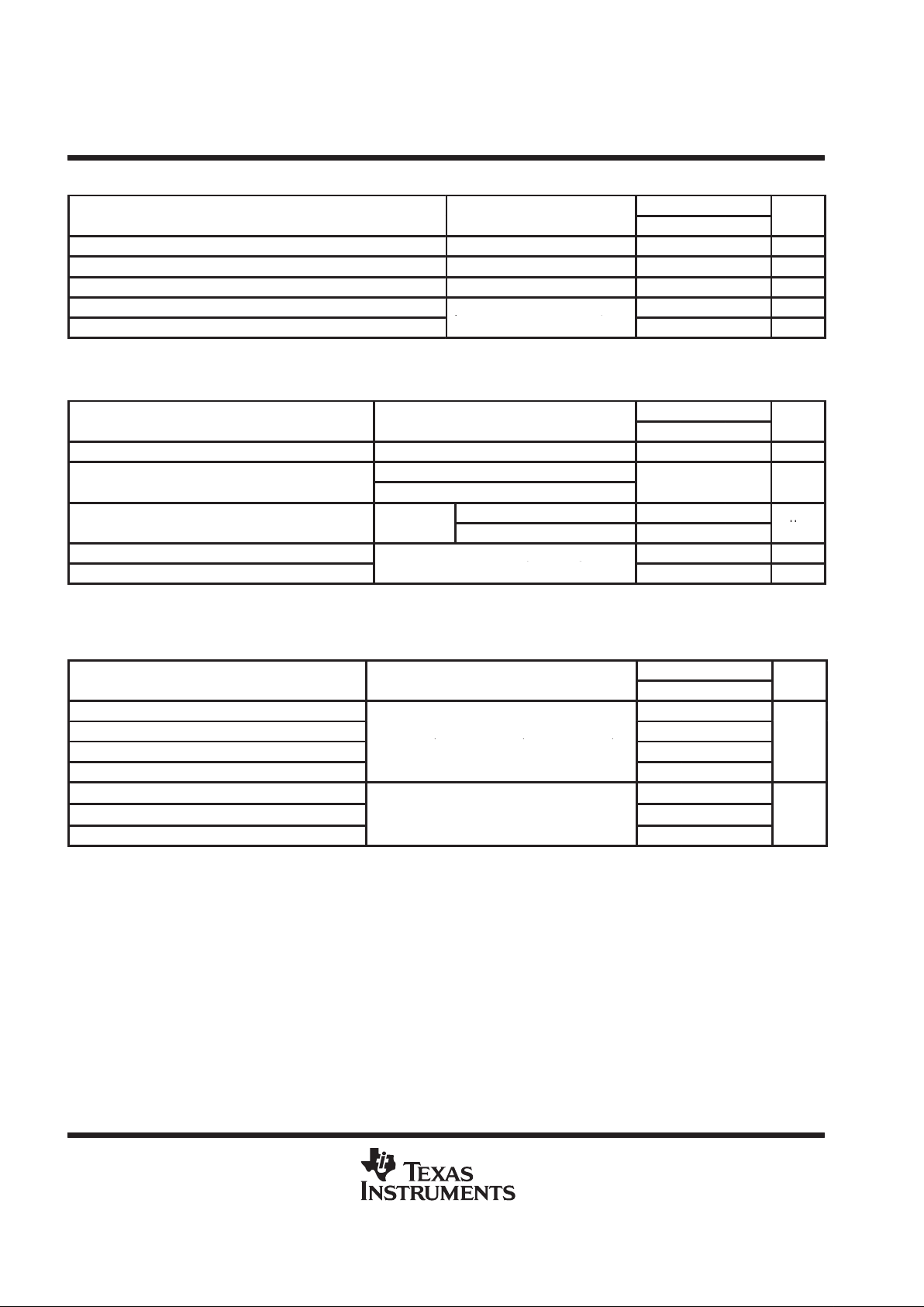
clamp diode characteristics, TC = 25°C
TPIC2701
PARAMETER
TEST CONDITIONS
MIN TYP MAX
UNIT
V
F
Forward on-voltage IF = 0.5 A 1 1.5 V
V
BR
Breakdown voltage IR = 1 µA 60 V
I
R
Reverse leakage current VR = 48 V 0.05 1 µA
t
rr(CD)
Reverse-recovery time
IF = 0.1 A, di/dt = 25 A/µs,
90 ns
Q
RR
Total source-drain diode charge
F
VCD = 48 V,µSee Figure 1
100 nC
clamp diode characteristics over operating case temperature range (unless otherwise noted)
(see Note 4)
TPIC2701M
PARAMETER
TEST CONDITIONS
MIN TYP MAX
UNIT
V
F
Forward voltage IF = 0.5 A 1 1.5 V
IR = 1 µA, TC = 25°C
V
(BR)
Breakdown voltage
IR = 1 mA
60
V
TC = 25°C 0.05 1
IRReverse leakage current
V
R
= 48
V
10
µ
A
t
rr(SD)
Reverse recovery time, source-to-drain
IF = 0.1 A, di/dt = 25 A/µs, TC = 25°C
90 ns
Q
RR
Total source-to-drain diode charge
F
VCD = 48 V,
µ
C
See Figure 1
100 nC
NOTE 4: Pulse testing techniques are used to maintain the virtual junction temperature as close to the case temperature as possible. Thermal
effects must be taken into account separately.
resistive-load switching characteristics, TC = 25°C
TPIC2701
PARAMETER
TEST CONDITIONS
MIN TYP MAX
UNIT
t
d(on)
Turn-on delay time 10
t
d(off)
Turn-off delay time
V
= 25 V, R
= 100 Ω,t
= 10 ns,
30
t
r
Rise time
DD
,
t
dis
= 10 ns,
L
,
See Figure 2
en
,
15
ns
t
f
Fall time 5
Q
g
Total gate charge
2.8 3.6
Q
gs
Gate-source charge
V
DS
= 48 V,
See
Figure
3
I
D
= 0.25 A,
V
GS
= 10 V,
1.6 2
nC
Q
gd
Gate-drain charge
See Figure 3
1.2 1.6
Page 5
TPIC2701
7-CHANNEL COMMON-SOURCE POWER DMOS ARRAY
SLIS019A – SEPTEMBER 1992 – REVISED SEPTEMBER 1996
5
POST OFFICE BOX 655303 • DALLAS, TEXAS 75265
resistive-load switching characteristics over operating case temperature range (unless otherwise
noted) (see Note 4)
TPIC2701M
PARAMETER
TEST CONDITIONS
MIN TYP MAX
UNIT
t
d(on)
Turn-on delay time 10
t
d(off)
Turn-off delay time
V
= 25 V, R
= 100 Ω,t
= 10 ns,
30
t
r
Rise time
DD
,
t
dis
= 10 ns,
L
,
See Figure 2
en
,
15
ns
t
f
Fall time 5
Q
g
Total gate charge
2.8
Q
gs
Gate-to-source charge
VDS = 48 V,
ID = 0.25 A, VGS = 10 V,
1.6
nC
Q
gd
Gate-to-drain charge
See Figure 3
1.2
NOTE 4: Pulse testing techniques are used to maintain the virtual junction temperature as close to the case temperature as possible. Thermal
effects must be taken into account separately.
thermal resistance
PARAMETER TEST CONDITIONS MIN TYP MAX UNIT
N package with all outputs at equal power 90
°
R
θJA
Junction-to-ambient thermal resistance
J package with all outputs at equal power 66
°C/W
PARAMETER MEASUREMENT INFORMATION
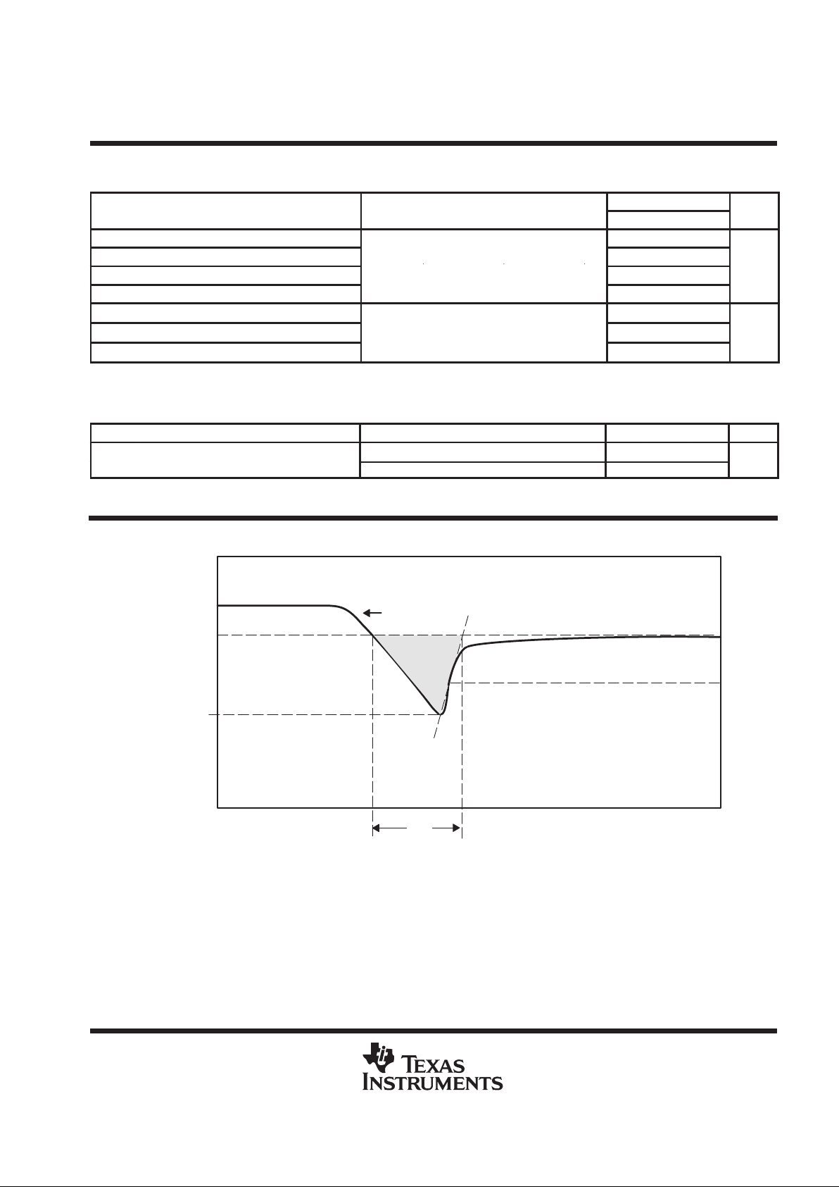
t
rr
0.5 A
IF/I
S
0
I
RM
di/dt = 25 A/µs
25% of I
RM
QRR = Shaded Area
(see Note A)
NOTE A: IRM = maximum recovery current
Figure 1. Reverse-Recovery-Current Waveforms of Source-Drain and Clamp Diodes
Page 6
TPIC2701
7-CHANNEL COMMON-SOURCE POWER DMOS ARRAY
SLIS019A – SEPTEMBER 1992 – REVISED SEPTEMBER 1996
6
POST OFFICE BOX 655303 • DALLAS, TEXAS 75265
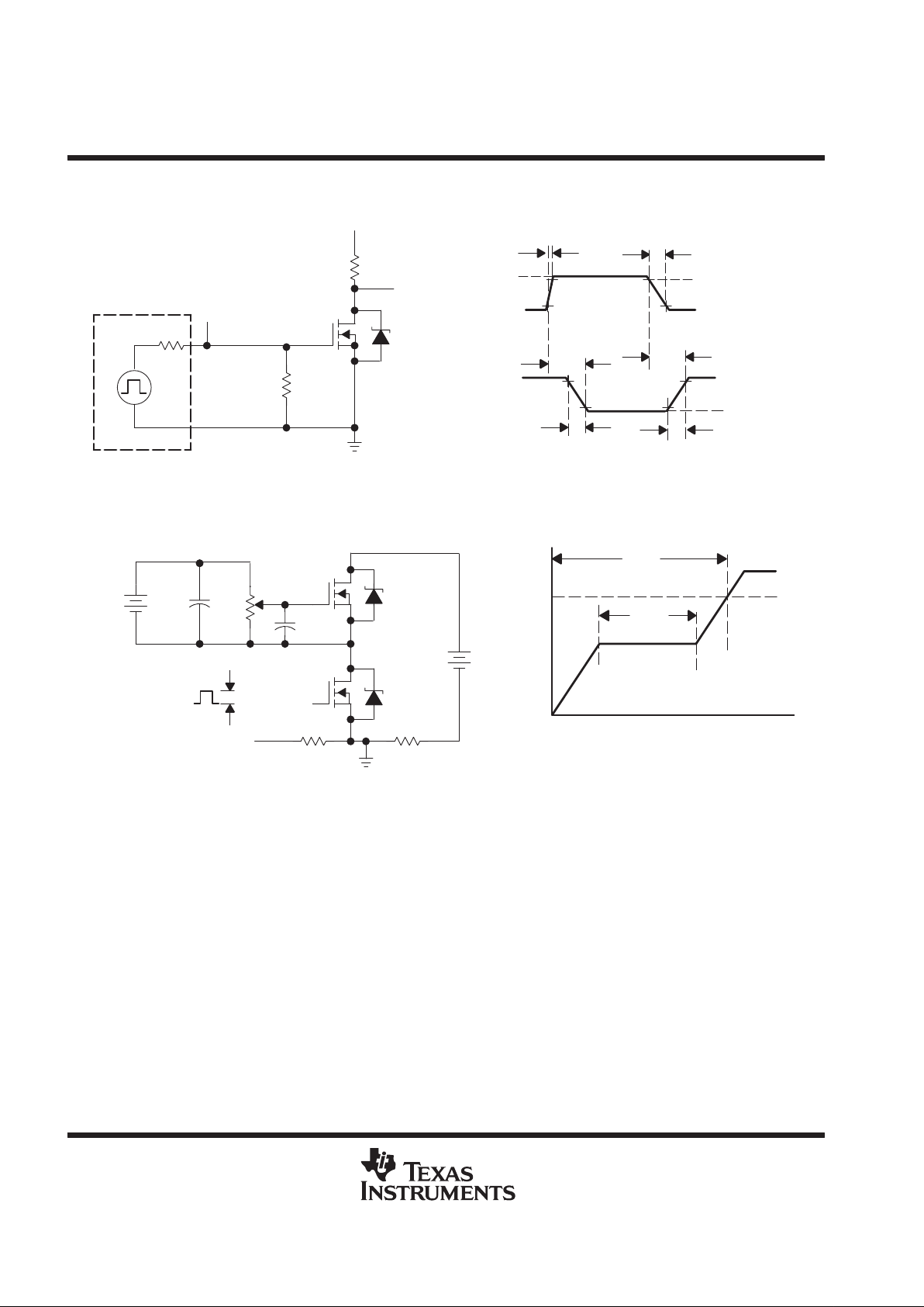
PARAMETER MEASUREMENT INFORMATION
Pulse Generator
50 Ω
R
gen
50 Ω
V
GS
25 V
DUT
V
DS
TEST CIRCUIT
R
L
V
DD
V
DS(on)
t
d(on)
t
f
t
d(off)
90%
10%
90%
10%
VOLTAGE WAVEFORM
V
GS
V
DS
15 V
0
t
r
90%
t
en
t
dis
Figure 2. Resistive Switching
Q
g
10 V
WAVEFORM
Q
gd
Time
Gate Voltage
V
GS
12-V
Battery
0.2 µF
50 kΩ
0.3 µF
Current
Regulator
DUT
Same Type
as DUT
0
IG = 100 µA
IG Current-
Sampling Resistor
ID Current-
Sampling Resistor
VDD = 48 V
Qgs = Qg – Q
gd
TEST CIRCUIT
Figure 3. Gate Charge Test Circuit and Waveform
Page 7
TPIC2701
7-CHANNEL COMMON-SOURCE POWER DMOS ARRAY
SLIS019A – SEPTEMBER 1992 – REVISED SEPTEMBER 1996
7
POST OFFICE BOX 655303 • DALLAS, TEXAS 75265
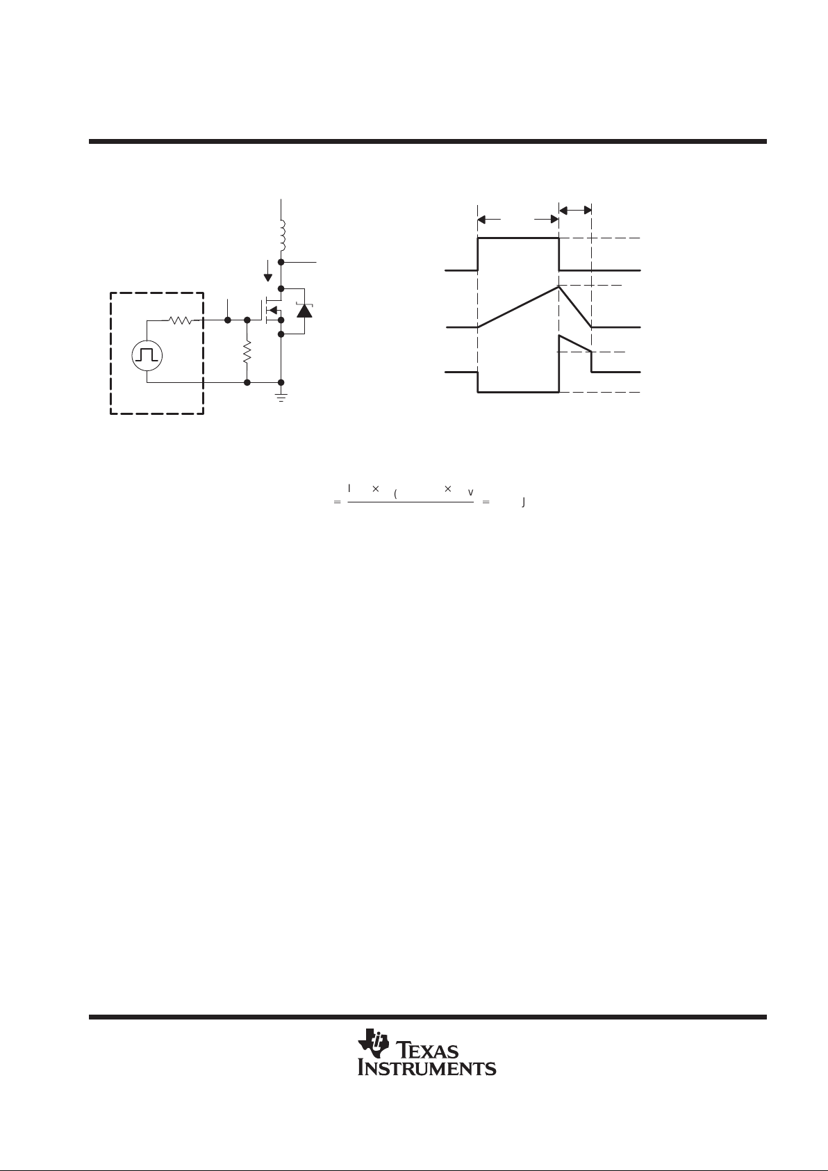
PARAMETER MEASUREMENT INFORMATION
25 V
4 mH
I
D
t
w
t
av
I
AS
V
(BR)DSX
= 60 V Min
VOLTAGE AND CURRENT WAVEFORMS
0
0
0
I
D
V
DS
DUT
V
DS
TEST CIRCUIT
(see Note A)
(see Note B)
Pulse Generator
50 Ω
R
gen
50 Ω
V
GS
V
GS
15 V
NOTES: A. The pulse generator has the following characteristics: tr ≤ 10 ns, tf ≤ 10 ns, ZO = 50 Ω.
B. Input pulse duration (tw) is increased until peak current IAS = 2.5 A.
Energy test level is defined as EAS+
IAS
V
(BR)DSX
t
av
2
+
22 mJ min.
Figure 4. Single-Pulse Avalanche Energy Test Circuit and Waveforms
Page 8
TPIC2701
7-CHANNEL COMMON-SOURCE POWER DMOS ARRAY
SLIS019A – SEPTEMBER 1992 – REVISED SEPTEMBER 1996
8
POST OFFICE BOX 655303 • DALLAS, TEXAS 75265
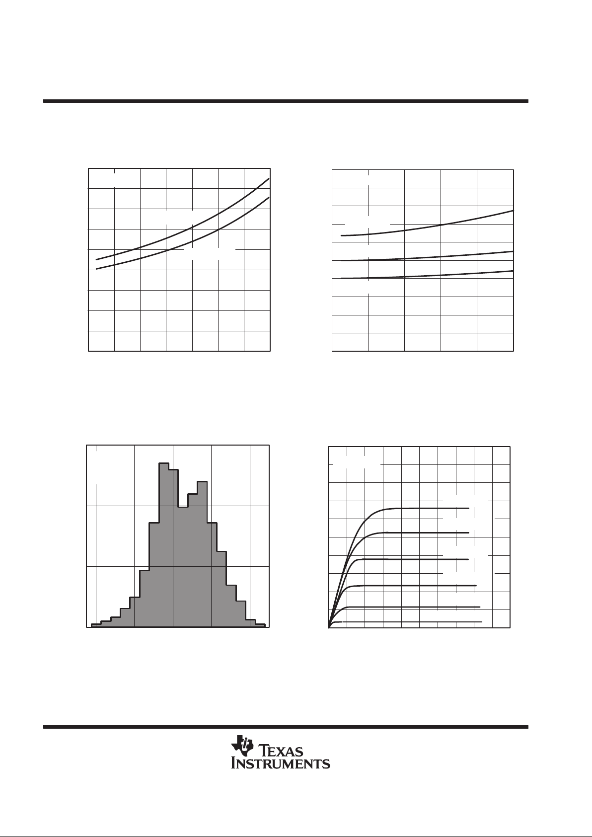
TYPICAL CHARACTERISTICS
0.3
0.2
0.1
0
0.4
0.5
0.6
0.7
0.8
STATIC DRAIN-SOURCE ON-STATE RESISTANCE
vs
FREE-AIR TEMPERATURE
TA – Free-Air Temperature – °C
ΩOn-State Resistance –
r
DS(on)
– Static Drain-Source
0.9
VGS = 15 V
VGS = 10 V
0 12550– 50 – 25 25 10075
STATIC DRAIN-SOURCE ON-STATE RESISTANCE
vs
DRAIN CURRENT
ID – Drain Current – A
ΩOn-State Resistance –
r
DS(on)
– Static Drain-Source
0.5
0.4
0.2
0.1
0
0.9
0.3
0 0.5 1 1.5
0.7
0.6
0.8
1
2 2.5
VGS = 6 V
VGS = 15 V
VGS = 20 V
ID = 0.5 A
TA = 25°C
Figure 5 Figure 6
5
0
0.76 0.775 0.79
10
15
0.805 0.82
DISTRIBUTION OF
FORWARD TRANSCONDUCTANCE
gfs – Forward Transconductance – S
Percentage of Units – %
2.5
2
1
0.5
0
4.5
1.5
0 2 10 14
3.5
3
4
5
20
DRAIN-TO-SOURCE CURRENT
vs
DRAIN-TO-SOURCE VOLTAGE
I – Drain-to-Source Current – A
D
VDS – Drain-to-Source Voltage – V
12 1816468
VGS = 5 V
VGS = 4.5 V
VGS = 4 V
VGS = 3.5 V
VGS = 3 V
TA = 25°C
ID = 0.5 A
VDS = 15 V
TA = 25°C
VGS = 2.5 V
Figure 7 Figure 8
Page 9

TPIC2701
7-CHANNEL COMMON-SOURCE POWER DMOS ARRAY
SLIS019A – SEPTEMBER 1992 – REVISED SEPTEMBER 1996
9
POST OFFICE BOX 655303 • DALLAS, TEXAS 75265
TYPICAL CHARACTERISTICS
GATE-SOURCE THRESHOLD VOLTAGE
vs
FREE-AIR TEMPERATURE
V
TGS
2.5
2
1
0.5
0
1.5
– Gate-Source Threshold Voltage – V
TA – Free-Air Temperature – °C
0 12550– 50 – 25 25 10075
ID = 10 mA
ID = 1 mA
GATE-SOURCE VOLTAGE
vs
GATE CHARGE
Q – Gate Charge – nC
10
8
4
2
0
6
0 0.3 1.5 2.1
14
12
16
3
1.8 2.72.40.6 0.9 1.2
18
20
V
GS
– Gate-Source Voltage – V
ID = 0.25 A
TA = 25°C
VDS = 20 V
VDS = 30 V
VDS = 48 V
Figure 9 Figure 10
SOURCE-TO-DRAIN DIODE CURRENT
vs
SOURCE-TO-DRAIN DIODE VOLTAGE
VSD – Source-to-Drain Diode Voltage – V
I
SD
2.5
2
1
0.5
0
1.5
0 0.2 1 1.4
3
21.2 1.81.60.4 0.6 0.8
– Source-to-Drain Diode Current – A
0.04
0.02
0.01
0.5 0.55 0.6 0.65 0.7 0.75 0.8
SOURCE-TO-DRAIN DIODE CURRENT
vs
SOURCE-TO-DRAIN DIODE VOLTAGE
0.85 0.9
0.1
0.07
0.4
0.2
1
0.7
VSD – Source-to-Drain Diode Voltage – V
– Source-to-Drain Diode Current – AI
SD
TA = 125°C
TA = 25°C
TA = 25°C
Figure 11 Figure 12
Page 10
TPIC2701
7-CHANNEL COMMON-SOURCE POWER DMOS ARRAY
SLIS019A – SEPTEMBER 1992 – REVISED SEPTEMBER 1996
10
POST OFFICE BOX 655303 • DALLAS, TEXAS 75265
TYPICAL CHARACTERISTICS
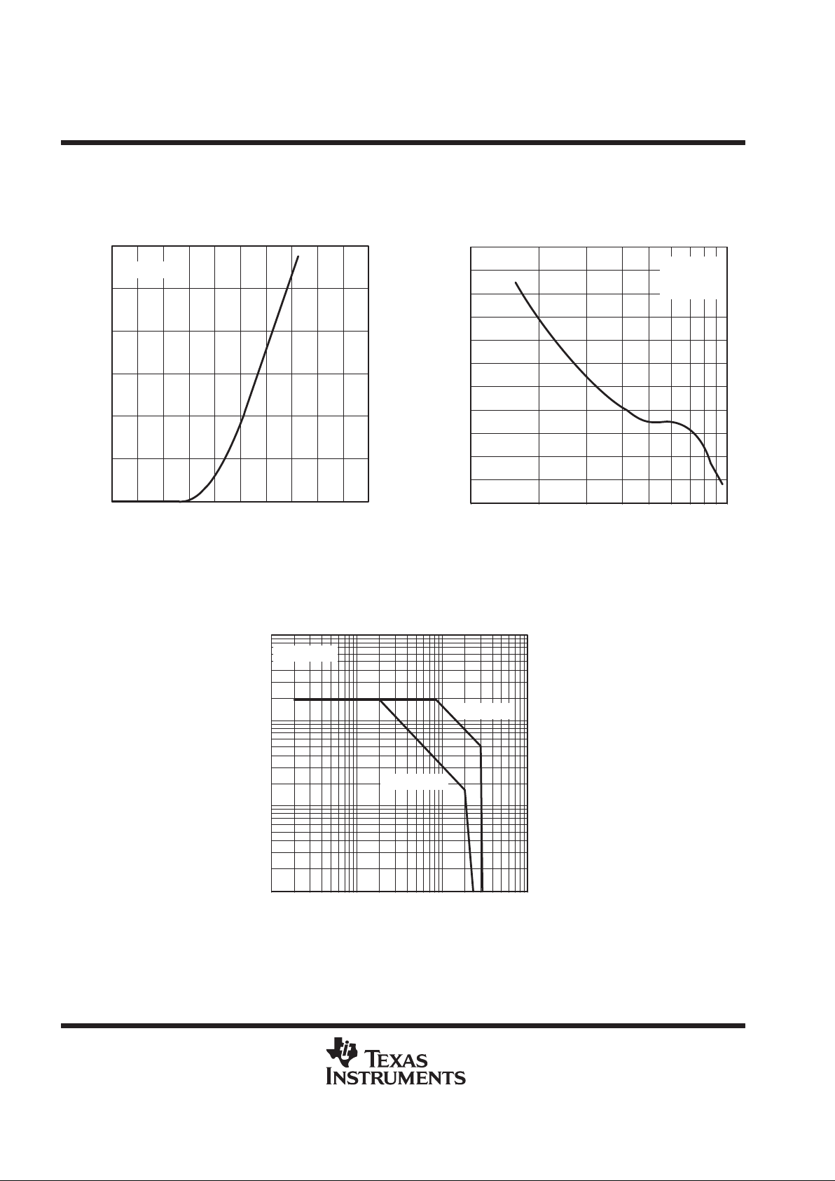
CLAMP-DIODE CURRENT
vs
CLAMP-DIODE VOLTAGE
Clamp-Diode Voltage – V
2.5
2
1
0.5
0
1.5
0 0.2 1 1.4
3
21.2 1.81.60.4 0.6 0.8
Clamp-Diode Current – A
CLAMP-DIODE REVERSE RECOVERY TIME
vs
REVERSE di/dt
Reverse di/dt – A/µs
80
70
50
40
30
120
60
10 20 60 80
100
90
110
130
1007030 40 50
– Clamp-Diode Reverse Recovery Time – ns
140
t
rr
IF = 0.1 A
VR = 48 V
TA = 25°C
TA = 25°C
Figure 13 Figure 14
REVERSE di/dt
vs
FORWARD CURRENT
IF – Forward Current – A
40
20
4
2
1
10
0.01
100
60
200
1010.1
600
1000
Reverse di/dt – A/
VCD = 40 V
VCD = 20 V
TA = 25°C
µs
6
400
NOTE A: VCD = V
clamp
– V
drain
Figure 15
Page 11
TPIC2701
7-CHANNEL COMMON-SOURCE POWER DMOS ARRAY
SLIS019A – SEPTEMBER 1992 – REVISED SEPTEMBER 1996
11
POST OFFICE BOX 655303 • DALLAS, TEXAS 75265
TYPICAL CHARACTERISTICS
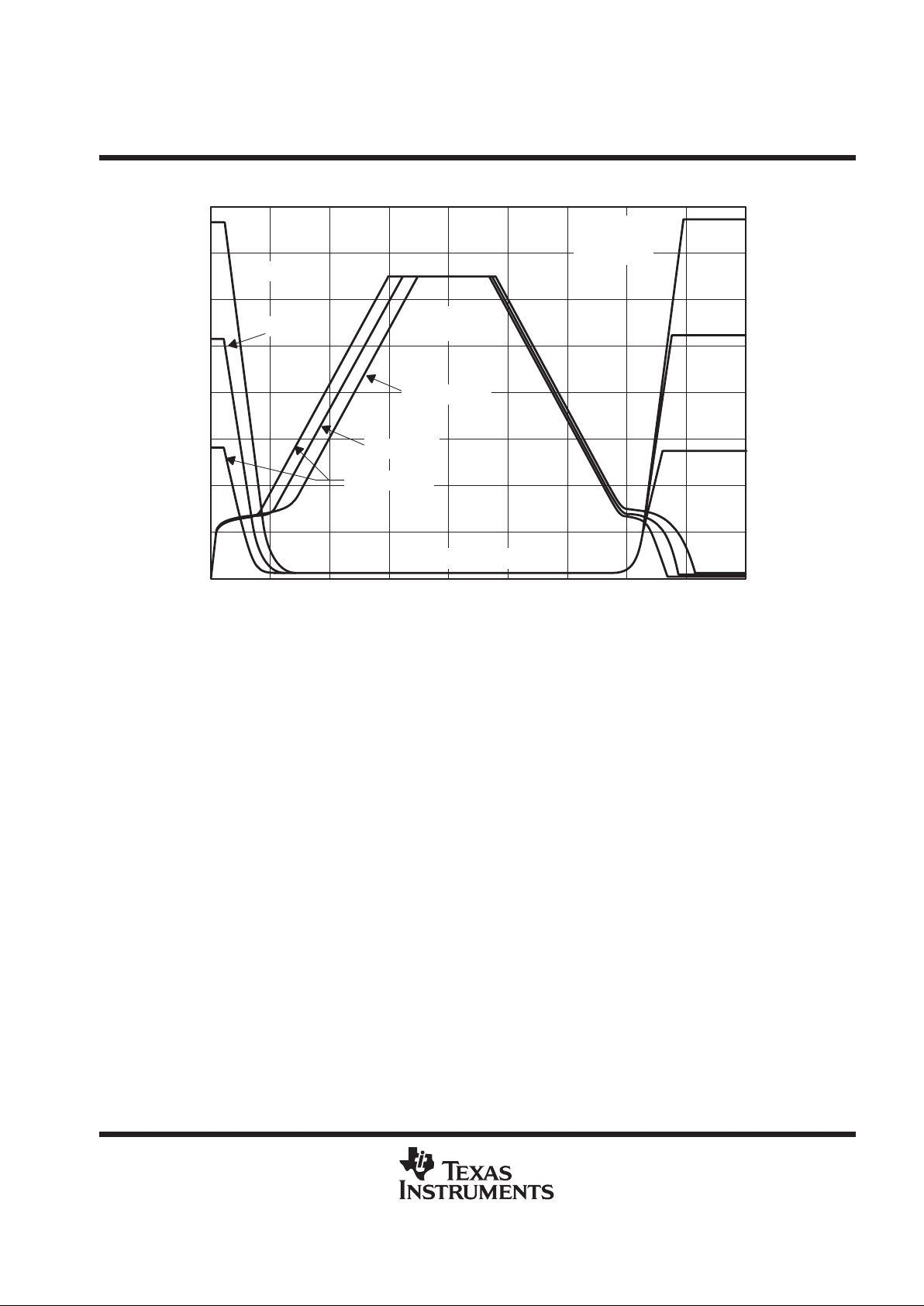
t – Time – µs
V
DS
– V
V
GS
– V
Drain-Source Voltage
–
Gate-Source Voltage
–
0 200 300 400 500 600 700 800 900
0
5
10
15
20
25
2
4
6
8
10
100
30
35
40
12
14
16
Drain-Source Voltage
Gate-Source
Voltage
RL = 2.5 Ω
IG = 10 µA
TA = 25°C
VDS = 25 V
VDS = 37.5 V
VDS = 12.5 V
VDS = 37.5 V
VDS = 25 V
Figure 16. Resistive Switching Waveforms
Page 12
TPIC2701
7-CHANNEL COMMON-SOURCE POWER DMOS ARRAY
SLIS019A – SEPTEMBER 1992 – REVISED SEPTEMBER 1996
12
POST OFFICE BOX 655303 • DALLAS, TEXAS 75265
THERMAL INFORMATION
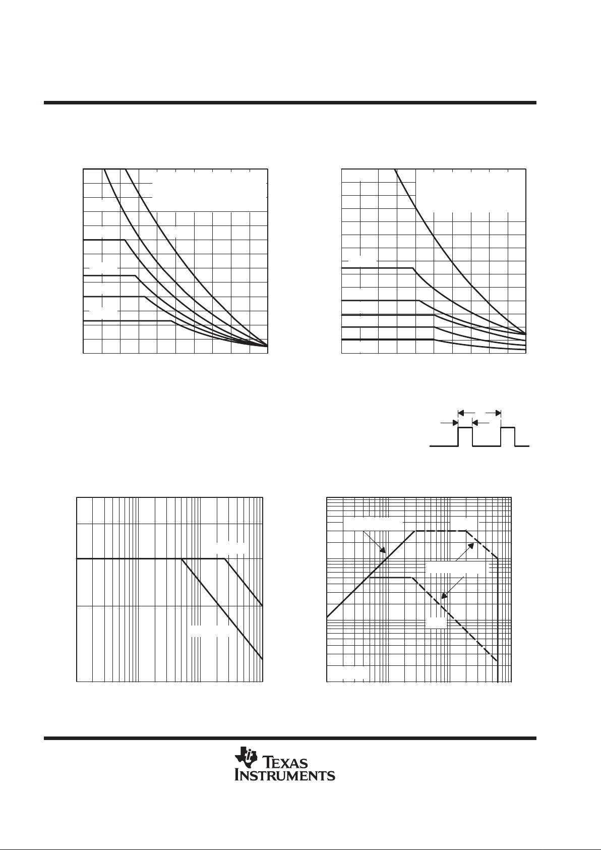
MAXIMUM DRAIN CURRENT
vs
DUTY CYCLE
Duty Cycle – %
1.4
1.2
0.8
0.6
0.4
1
010 50 70
1.8
1.6
2
100
60 908020 30 40
2.2
2.4
I
D
– Maximum Drain Current – A
N = 1
2.6
2.8
3
N = 2
N = 3
N = 4
N = 5
N = 7
TA = 25°C
N = Number of Outputs
Conducting Simultaneously
See Note A
1.4
1.2
0.8
0.6
0.4
1
010 50 70
1.8
1.6
2
100
60 908020 30 40
2.2
2.4
I
CL
– Maximum Clamp-Diode Current – A
2.6
2.8
3
MAXIMUM CLAMP-DIODE CURRENT
vs
DUTY CYCLE
Duty Cycle – %
N = 1
N = 2
N = 3
N = 4
N = 5
N = 7
TA = 25°C
N = Number of Outputs
Conducting Simultaneously
See Note A
0.2
Figure 17 Figure 18
NOTE A: For Figures 17 and 18, d = tw/tc = 10 ms / tc, where tw and tc are defined by the following:
t
c
t
w
5
4
0.001 0.1
PEAK AVALANCHE CURRENT
vs
TIME DURATION OF AVALANCHE
0.01 1
2
1
I
AS
– Peak Avalanche Current – A
tav – Time Duration of Avalanche – ms
3
TA = 25°C
MAXIMUM DRAIN CURRENT
vs
DRAIN-SOURCE VOLTAGE
VDS – Drain-To-Source Voltage – V
0.4
0.2
0.04
0.02
0.01
0.1
0.1
1
0.6
2
100101
6
10
– Maximum Drain-Diode DCurrent – A
0.06
4
I
D
r
DS(on)
Limit
DC
Thermal Limit
1 ms
TA = 25°C
TA = 125°C
Figure 19 Figure 20
Page 13
TPIC2701
7-CHANNEL COMMON-SOURCE POWER DMOS ARRAY
SLIS019A – SEPTEMBER 1992 – REVISED SEPTEMBER 1996
13
POST OFFICE BOX 655303 • DALLAS, TEXAS 75265
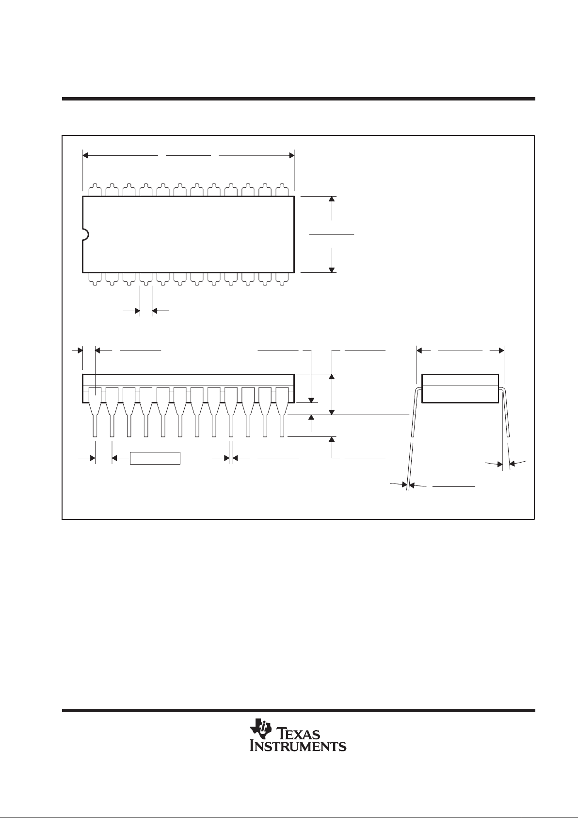
MECHANICAL INFORMATION
JW (R-GDIP-T24) CERAMIC DUAL-IN-LINE PACKAGE
4040111/B 04/95
0.515 (13,10)
0.560 (14,20)
0.225 (5,70)
0.150 (3,80)
0.610 (15,50)
0.590 (14,99)
0.008 (0,20)
0.012 (0,30)
0.125 (3,17)
0.160 (4,06)
Seating Plane
13
12
0.020 (0,51)
0.070 (1,78)
0.060 (1,52)
0.100 (2,54)
1.235 (31,30)
0.070 (1,78) MAX
1.290 (32,80)
24
1
0.020 (0,51)
0.016 (0,41)
0°–15°
0.100 (2,54)
NOTES: A. All linear dimensions are in inches (millimeters).
B. This drawing is subject to change without notice.
C. This package can be hermetically sealed with a ceramic lid using glass frit.
D. Index point is provided on cap for terminal identification only on press ceramic glass frit seal only
E. Falls within MIL-STD-1835 GDIP5-T24
Page 14
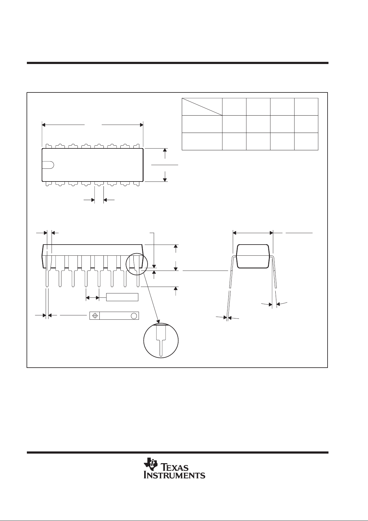
TPIC2701
7-CHANNEL COMMON-SOURCE POWER DMOS ARRAY
SLIS019A – SEPTEMBER 1992 – REVISED SEPTEMBER 1996
14
POST OFFICE BOX 655303 • DALLAS, TEXAS 75265
MECHANICAL INFORMATION
N (R-PDIP-T**) PLASTIC DUAL-IN-LINE PACKAGE
20
0.975
(24,77)
0.940
(23,88)
18
0.920
0.850
14
0.775
0.745
(19,69)
(18,92)
16
0.775
(19,69)
(18,92)
0.745
A MIN
DIM
A MAX
PINS **
0.310 (7,87)
0.290 (7,37)
(23.37)
(21.59)
Seating Plane
0.010 (0,25) NOM
14/18 PIN ONL Y
4040049/C 08/95
9
8
0.070 (1,78) MAX
A
0.035 (0,89) MAX
0.020 (0,51) MIN
16
1
0.015 (0,38)
0.021 (0,53)
0.200 (5,08) MAX
0.125 (3,18) MIN
0.240 (6,10)
0.260 (6,60)
M
0.010 (0,25)
0.100 (2,54)
0°–15°
16 PIN SHOWN
NOTES: A. All linear dimensions are in inches (millimeters).
B. This drawing is subject to change without notice.
C. Falls within JEDEC MS-001 (20 pin package is shorter then MS-001.)
Page 15

IMPORTANT NOTICE
T exas Instruments and its subsidiaries (TI) reserve the right to make changes to their products or to discontinue
any product or service without notice, and advise customers to obtain the latest version of relevant information
to verify, before placing orders, that information being relied on is current and complete. All products are sold
subject to the terms and conditions of sale supplied at the time of order acknowledgement, including those
pertaining to warranty, patent infringement, and limitation of liability.
TI warrants performance of its semiconductor products to the specifications applicable at the time of sale in
accordance with TI’s standard warranty. Testing and other quality control techniques are utilized to the extent
TI deems necessary to support this warranty. Specific testing of all parameters of each device is not necessarily
performed, except those mandated by government requirements.
CERT AIN APPLICATIONS USING SEMICONDUCTOR PRODUCTS MAY INVOLVE POTENTIAL RISKS OF
DEATH, PERSONAL INJURY, OR SEVERE PROPERTY OR ENVIRONMENTAL DAMAGE (“CRITICAL
APPLICATIONS”). TI SEMICONDUCTOR PRODUCTS ARE NOT DESIGNED, AUTHORIZED, OR
WARRANTED TO BE SUITABLE FOR USE IN LIFE-SUPPORT DEVICES OR SYSTEMS OR OTHER
CRITICAL APPLICATIONS. INCLUSION OF TI PRODUCTS IN SUCH APPLICA TIONS IS UNDERST OOD TO
BE FULLY AT THE CUSTOMER’S RISK.
In order to minimize risks associated with the customer’s applications, adequate design and operating
safeguards must be provided by the customer to minimize inherent or procedural hazards.
TI assumes no liability for applications assistance or customer product design. TI does not warrant or represent
that any license, either express or implied, is granted under any patent right, copyright, mask work right, or other
intellectual property right of TI covering or relating to any combination, machine, or process in which such
semiconductor products or services might be or are used. TI’s publication of information regarding any third
party’s products or services does not constitute TI’s approval, warranty or endorsement thereof.
Copyright 1998, Texas Instruments Incorporated
 Loading...