

Texas Instruments TPIC6273N, TPIC6273DW Datasheet
TPIC6273
POWER LOGIC OCTAL D-TYPE LATCH
SLIS01 1A – APRIL 1992 – REVISED OCTOBER 1995
• Low r
DS(on)
. . . 1.3 Ω Typ
• Avalanche Energy . . . 75 mJ
• Eight Power DMOS Transistor Outputs of
250-mA Continuous Current
• 1.5-A Pulsed Current Per Output
• Output Clamp Voltage up to 45 V
• Low Power Consumption
description
The TPIC6273 is a monolithic high-voltage
high-current power logic octal D-type latch with
DMOS transistor outputs designed for use in
systems that require relatively high load power.
The device contains a built-in voltage clamp on the
outputs for inductive transient protection. Power
driver applications include relays, solenoids, and
other medium-current or high-voltage loads.
The TPIC6273 contains eight positive-edgetriggered D-type flip-flops with a direct clear input.
Each flip-flop features an open-drain power
DMOS transistor output.
When clear (CLR
inputs meeting the setup time requirements is
transferred to the DRAIN outputs on the positivegoing edge of the clock pulse. Clock triggering
occurs at a particular voltage level and is not
directly related to the transition time of the
positive-going pulse. When the clock input (CLK)
is at either the high or low level, the D input signal
has no effect at the output. An asynchronous CLR
is provided to turn all eight DMOS-transistor
outputs off.
The TPIC6273 is characterized for operation over
the operating case temperature range of –40°C
to 125°C.
) is high, information at the D
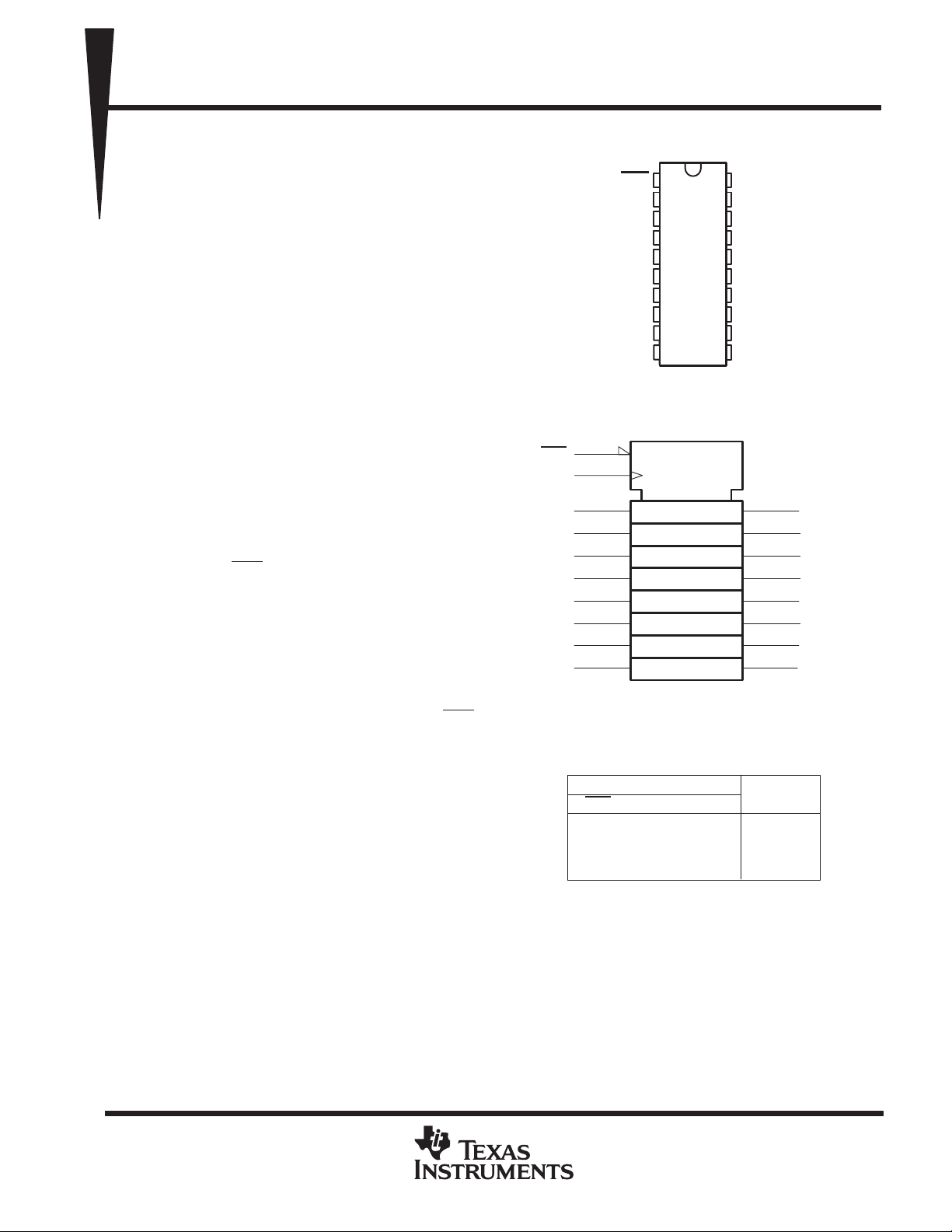
DW OR N PACKAGE
(TOP VIEW)
CLR
1
D1
2
D2
3
DRAIN1
DRAIN2
DRAIN3
DRAIN4
GND
logic symbol
CLR
CLK
D1
D2
D3
D4
D5
D6
D7
D8
†
This symbol is in accordance with ANSI/IEEE Standard 91-1984
and IEC Publication 617-12.
†
1
11
2
3
8
9
12
13
18
19
CLR
L
H
H
H
H = high level, L = low level, X = irrelevant
4
5
6
7
8
D3
9
D4
10
R
C1
1D
FUNCTION TABLE
(each channel)
INPUTS
CLK D
X
↑
↑
L
20
19
18
17
16
15
14
13
12
11
X
H
L
X
V
CC
D8
D7
DRAIN8
DRAIN7
DRAIN6
DRAIN5
D6
D5
CLK
OUTPUT
DRAIN
H
L
H
Latched
14
15
16
17
4
5
6
7
DRAIN1
DRAIN2
DRAIN3
DRAIN4
DRAIN5
DRAIN6
DRAIN7
DRAIN8
PRODUCTION DATA information is current as of publication date.
Products conform to specifications per the terms of Texas Instruments
standard warranty. Production processing does not necessarily include
testing of all parameters.
POST OFFICE BOX 655303 • DALLAS, TEXAS 75265
Copyright 1995, Texas Instruments Incorporated
1
TPIC6273
POWER LOGIC OCTAL D-TYPE LATCH
SLIS01 1A – APRIL 1992 – REVISED OCTOBER 1995
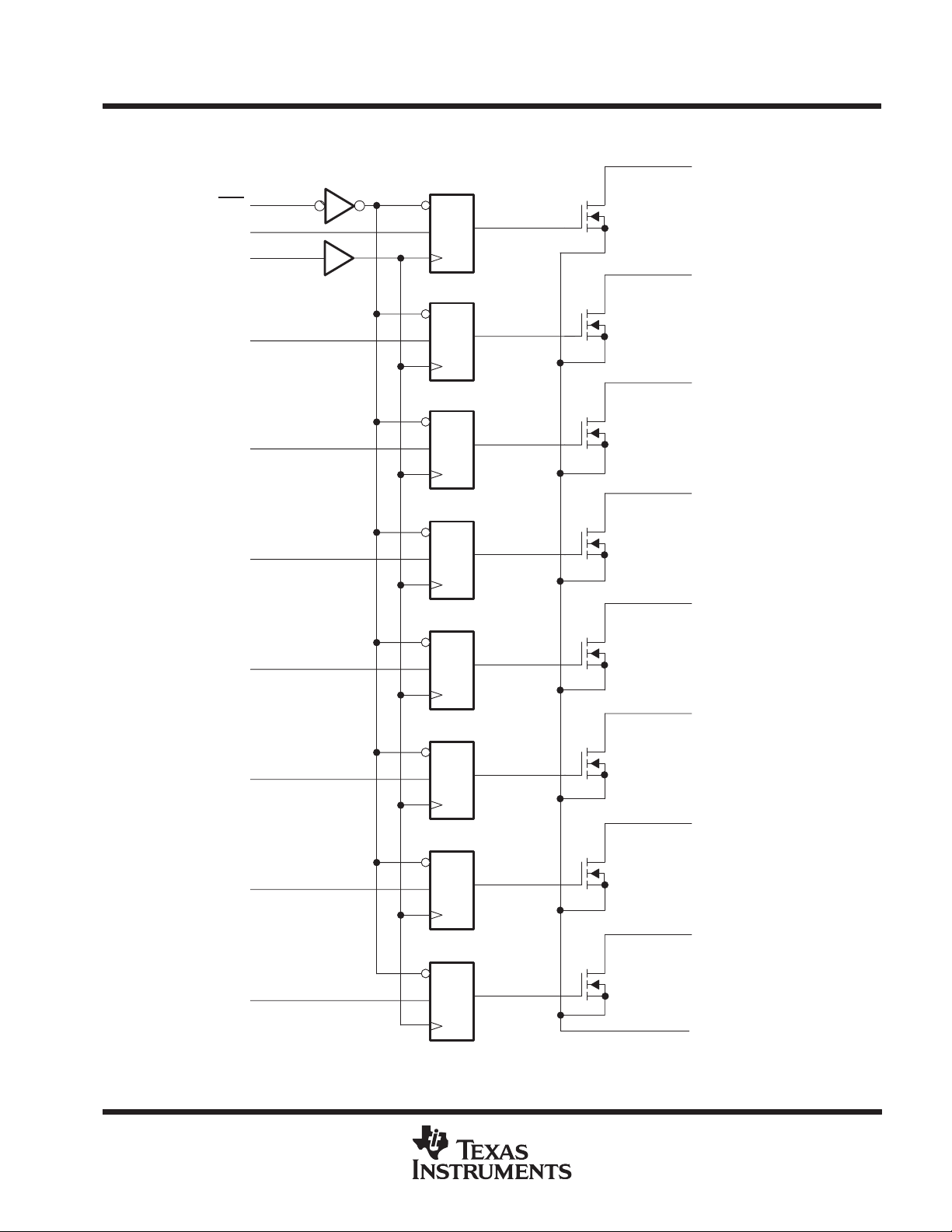
logic diagram (positive logic)
4
DRAIN1
CLR
D1
CLK
D2
D3
D4
D5
1
2
11
3
8
9
12
R
1D
R
1D
R
1D
R
1D
R
1D
C1
C1
C1
C1
C1
5
6
7
14
15
DRAIN2
DRAIN3
DRAIN4
DRAIN5
DRAIN6
R
13
D6
18
D7
19
D8
2
POST OFFICE BOX 655303 • DALLAS, TEXAS 75265
1D
R
1D
R
1D
C1
C1
C1
16
17
10
DRAIN7
DRAIN8
GND
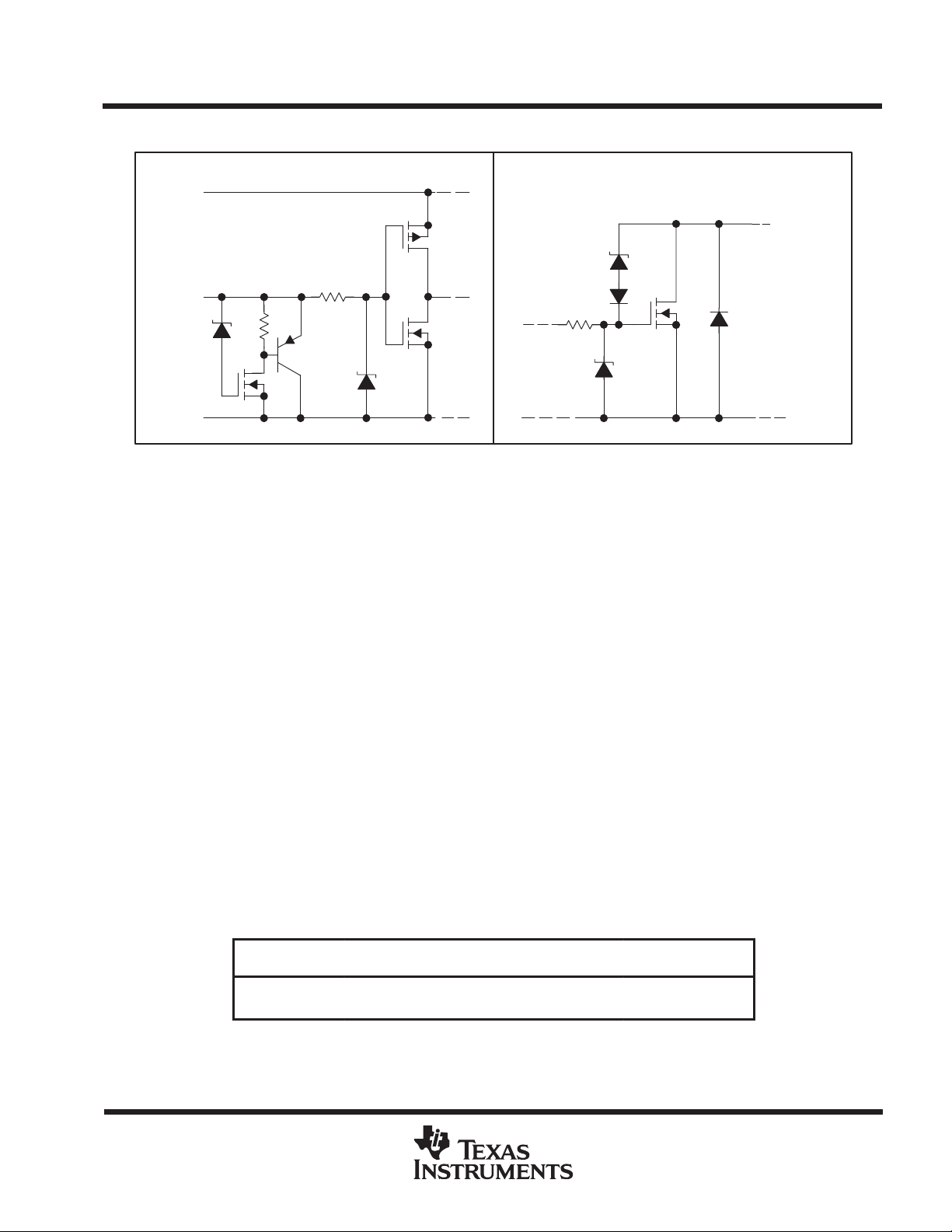
schematic of inputs and outputs
EQUIVALENT OF EACH INPUT TYPICAL OF ALL DRAIN OUTPUTS
V
CC
Input
25 V
TPIC6273
POWER LOGIC OCTAL D-TYPE LATCH
SLIS01 1A – APRIL 1992 – REVISED OCTOBER 1995
DRAIN
45 V
12 V
GND
12 V
GND
absolute maximum ratings over recommended operating case temperature range (unless
otherwise noted)
Logic supply voltage, V
Logic input voltage range, V
Power DMOS drain-to-source voltage, V
Continuous source-drain diode anode current 1 A. . . . . . . . . . . . . . . . . . . . . . . . . . . . . . . . . . . . . . . . . . . . . . . . . .
Pulsed source-drain diode anode current 2 A. . . . . . . . . . . . . . . . . . . . . . . . . . . . . . . . . . . . . . . . . . . . . . . . . . . . . .
Pulsed drain current, each output, all outputs on, I
Continuous drain current, each output, all outputs on, I
Peak drain current single output, I
Single-pulse avalanche energy, E
Avalanche current, I
Continuous total power dissipation See Dissipation Rating Table. . . . . . . . . . . . . . . . . . . . . . . . . . . . . . . . . . . . .
Operating virtual junction temperature range, T
Storage temperature range, T
Lead temperature 1,6 mm (1/16 inch) from case for 10 seconds 260°C. . . . . . . . . . . . . . . . . . . . . . . . . . . . . .
†
Stresses beyond those listed under “absolute maximum ratings” may cause permanent damage to the device. These are stress ratings only, and
functional operation of the device at these or any other conditions beyond those indicated under “recommended operating conditions” is not
implied. Exposure to absolute-maximum-rated conditions for extended periods may affect device reliability.
NOTES: 1. All voltage values are with respect to GND.
2. Each power DMOS source is internally connected to GND.
3. Pulse duration ≤ 100 µs, duty cycle ≤ 2%
4. DRAIN supply voltage = 15 V , starting junction temperature (TJS) = 25°C, L = 100 mH, IAS = 1 A (see Figure 4).
†
(see Note 1) 7 V. . . . . . . . . . . . . . . . . . . . . . . . . . . . . . . . . . . . . . . . . . . . . . . . . . . . . . .
CC
–0.3 V to 7 V. . . . . . . . . . . . . . . . . . . . . . . . . . . . . . . . . . . . . . . . . . . . . . . . . . . . . . . .
I
DM,TA
(see Note 4) 1 A. . . . . . . . . . . . . . . . . . . . . . . . . . . . . . . . . . . . . . . . . . . . . . . . . . . . . . . . . .
AS
AS
–65°C to 150°C. . . . . . . . . . . . . . . . . . . . . . . . . . . . . . . . . . . . . . . . . . . . . . . . . .
stg
(see Note 2) 45 V. . . . . . . . . . . . . . . . . . . . . . . . . . . . . . . . . . . . . . .
DS
T
= 25°C (see Note 3) 750 mA. . . . . . . . . . . . . . . . . . .
Dn,
A
T
= 25°C 250 mA. . . . . . . . . . . . . . . . . . . . . . . . . .
Dn,
= 25°C (see Note 3) 2 A. . . . . . . . . . . . . . . . . . . . . . . . . . . . . . . . . . . . .
A
(see Figure 4) 75 mJ. . . . . . . . . . . . . . . . . . . . . . . . . . . . . . . . . . . . . . . . . . .
–40°C to 150°C. . . . . . . . . . . . . . . . . . . . . . . . . . . . . . . . . . . .
J
DISSIPATION RATING TABLE
PACKAGE
DW 1125 mW 9.0 mW/°C 225 mW
N 1150 mW 9.2 mW/°C 230 mW
TA ≤ 25°C
POWER RATING
POST OFFICE BOX 655303 • DALLAS, TEXAS 75265
DERATING FACTOR
ABOVE TA = 25°C
TA = 125°C
POWER RATING
3
 Loading...