Texas Instruments TPIC6259DWR, TPIC6259N, TPIC6259DW Datasheet

TPIC6259
POWER LOGIC 8-BIT ADDRESSABLE LATCH
SLIS009A – APIRL 1992 – REVISED SEPTEMBER 1995
Copyright 1995, Texas Instruments Incorporated
1
POST OFFICE BOX 655303 • DALLAS, TEXAS 75265
POST OFFICE BOX 1443
• HOUSTON, TEXAS 77251–1443
• Low r
DS(on)
. . . 1.3 Ω Typical
• Avalanche Energy...75 mJ
•Eight Power DMOS Transistor Outputs of
250-mA Continuous Current
• 1.5-A Pulsed Current Per Output
• Output Clamp Voltage at 45 V
• Four Distinct Function Modes
• Low Power Consumption
description
This power logic 8-bit addressable latch controls
open-drain DMOS transistor outputs and is
designed for general-purpose storage applications in digital systems. Specific uses include
working registers, serial-holding registers, and
decoders or demultiplexers. This is a multifunctional device capable of storing single-line
data in eight addressable latches with 3-to-8
decoding or demultiplexing mode active-low
DMOS outputs.
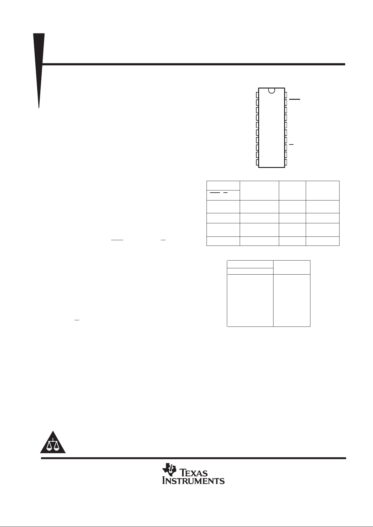
Four distinct modes of operation are selectable by
controlling the clear (CLR
) and enable (G) inputs
as enumerated in the function table. In the
addressable-latch mode, data at the data-in (D)
terminal is written into the addressed latch. The
addressed DMOS transistor output inverts the
data input with all unaddressed DMOS-transistor
outputs remaining in their previous states. In the
memory mode, all DMOS-transistor outputs
remain in their previous states and are unaffected
by the data or address inputs. To eliminate the
possibility of entering erroneous data in the latch,
enable G
should be held high (inactive) while the
address lines are changing. In the 3-to-8 decoding
or demultiplexing mode, the addressed output is inverted with respect to the D input and all other outputs are
high. In the clear mode, all outputs are high and unaffected by the address and data inputs.
Separate power and logic level ground pins are provided to facilitate maximum system flexibility . Pins 1, 10, 1 1,
and 20 are internally connected, and each pin must be externally connected to the power system ground in order
to minimize parasitic inductance. A single-point connection between pin 9, logic ground (LGND), and pins 1, 10,
11, and 20, power ground (PGND) must be externally made in a manner that reduces crosstalk between the
logic and load circuits.
The TPIC6259 is characterized for operation over the operating case temperature range of –40°C to 125°C.
Please be aware that an important notice concerning availability, standard warranty, and use in critical applications of
Texas Instruments semiconductor products and disclaimers thereto appears at the end of this data sheet.
1
2
3
4
5
6
7
8
9
10
20
19
18
17
16
15
14
13
12
11
PGND
V
CC
S0
DRAIN0
DRAIN1
DRAIN2
DRAIN3
S1
LGND
PGND
PGND
CLR
D
DRAIN7
DRAIN6
DRAIN5
DRAIN4
G
S2
PGND
DW OR N PACKAGE
(TOP VIEW)
OUTPUT OF
ADDRESSED
DRAIN
EACH
OTHER
DRAIN
INPUTS
FUNCTION
CLR G
FUNCTION TABLE
LATCH SELECTION TABLE
SELECT INPUTS DRAIN
ADDRESSED
0
1
2
3
4
5
6
7
L
L
L
L
H
H
H
H
D
HHLLH
L
L
H
Q
io
Q
io
Q
io
Q
io
H H X Memory
LLLLH
L
L
H
H
H
8-Line
Demultiplexer
L H X H H Clear
Addressable
Latch
S2 S1 S0
L
L
H
H
L
L
H
H
L
H
L
H
L
H
L
H
PRODUCTION DATA information is current as of publication date.
Products conform to specifications per the terms of Texas Instruments
standard warranty. Production processing does not necessarily include
testing of all parameters.

TPIC6259
POWER LOGIC 8-BIT ADDRESSABLE LATCH
SLIS009A – APIRL 1992 – REVISED SEPTEMBER 1995
2
POST OFFICE BOX 655303 • DALLAS, TEXAS 75265
POST OFFICE BOX 1443
• HOUSTON, TEXAS 77251–1443
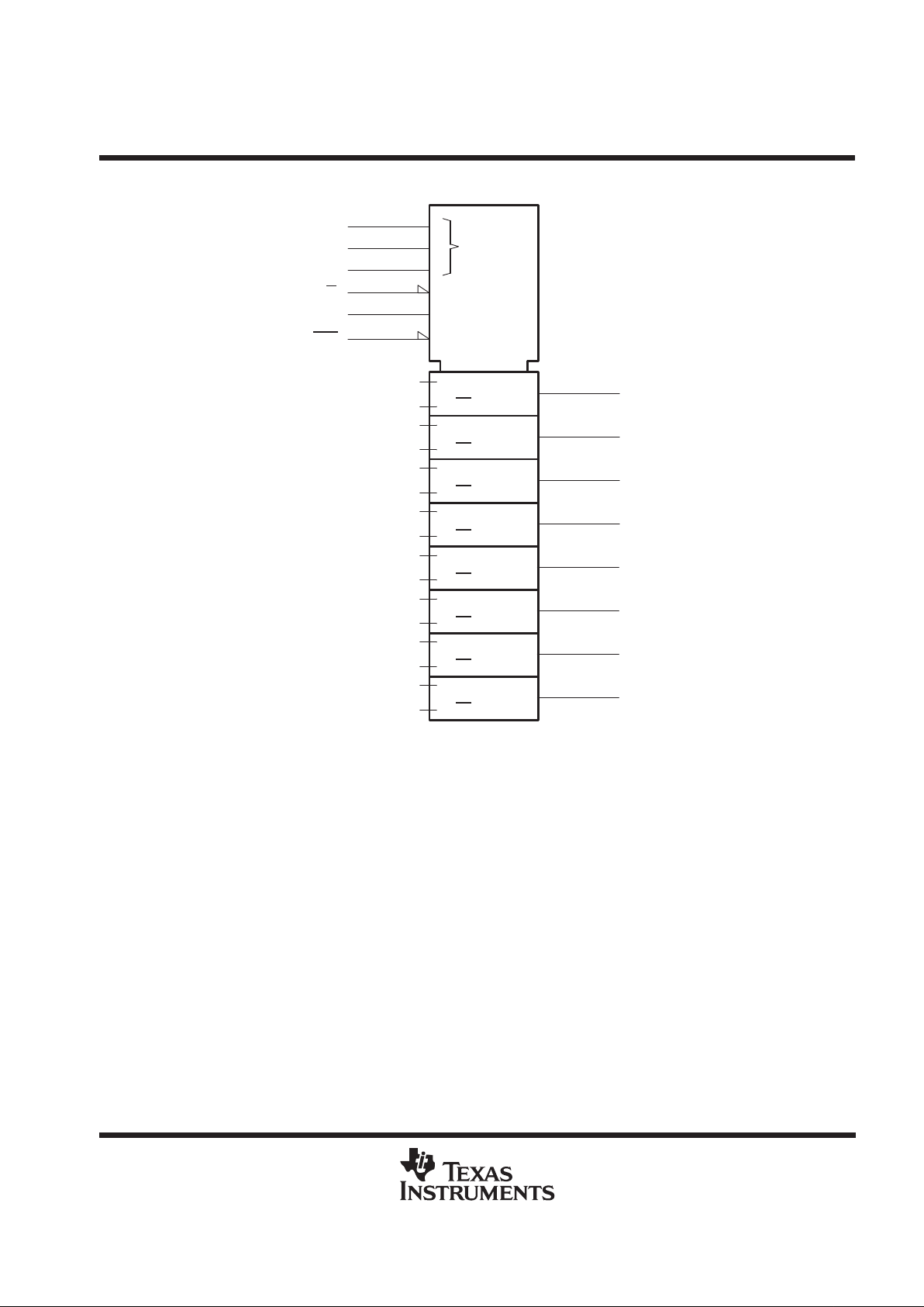
logic symbol
†
0
3
S0
8
S1
2
12
S2
G8
13
Z9
18
D
Z10
19
8M 0/7
9,0D
9,1D
9,2D
9,3D
9,4D
9,5D
9,6D
9,7D
10,0R
DRAIN0
4
DRAIN1
5
DRAIN2
6
DRAIN3
7
DRAIN4
14
DRAIN5
15
DRAIN6
16
DRAIN7
17
10,1R
10,2R
10,3R
10,4R
10,5R
10,6R
10,7R
G
CLR
†
This symbol is in accordance with ANSI/IEEE Std 91-1984 and IEC Publication 617-12.

TPIC6259
POWER LOGIC 8-BIT ADDRESSABLE LATCH
SLIS009A – APIRL 1992 – REVISED SEPTEMBER 1995
3
POST OFFICE BOX 655303 • DALLAS, TEXAS 75265
POST OFFICE BOX 1443
• HOUSTON, TEXAS 77251–1443
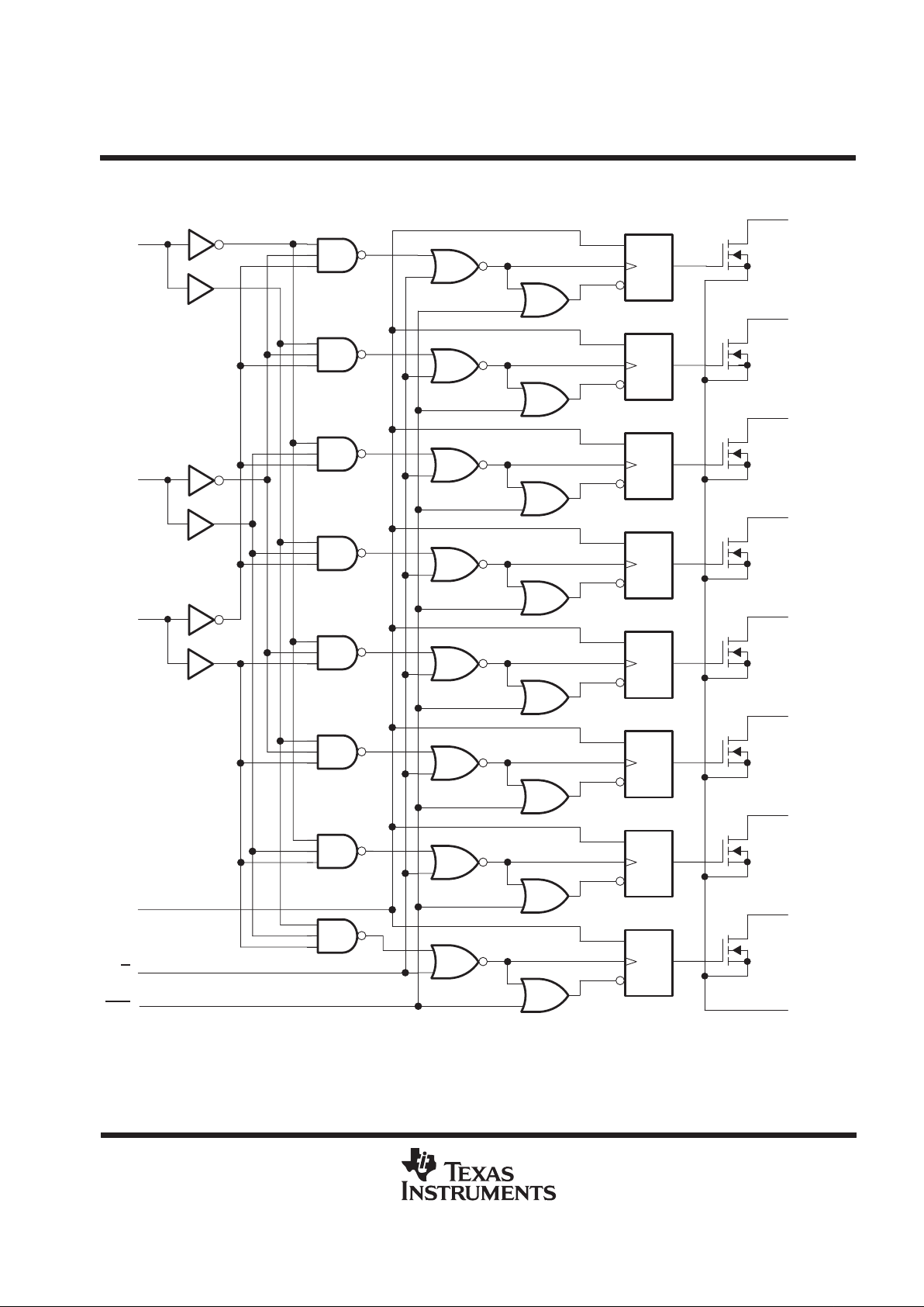
logic diagram (positive logic)
D
C1
CLR
S0
D
C1
CLR
S2
S1
D
G
CLR
D
C1
CLR
D
C1
CLR
D
C1
CLR
D
C1
CLR
D
C1
CLR
D
C1
CLR
4
DRAIN0
5
DRAIN1
6
DRAIN2
7
DRAIN3
14
DRAIN4
15
DRAIN5
16
DRAIN6
17
DRAIN7
1,10,11, 20
PGND
3
12
8
18
13
19
 Loading...