

Page 1
H-BRIDGE GATE-PROTECTED
POWER DMOS ARRAY
SLIS024A – DECEMBER 1993 – REVISED MARCH 1994
D
Low r
DS(on)
D
High Voltage Output...60 V
D
Extended ESD Capability...4000 V
description
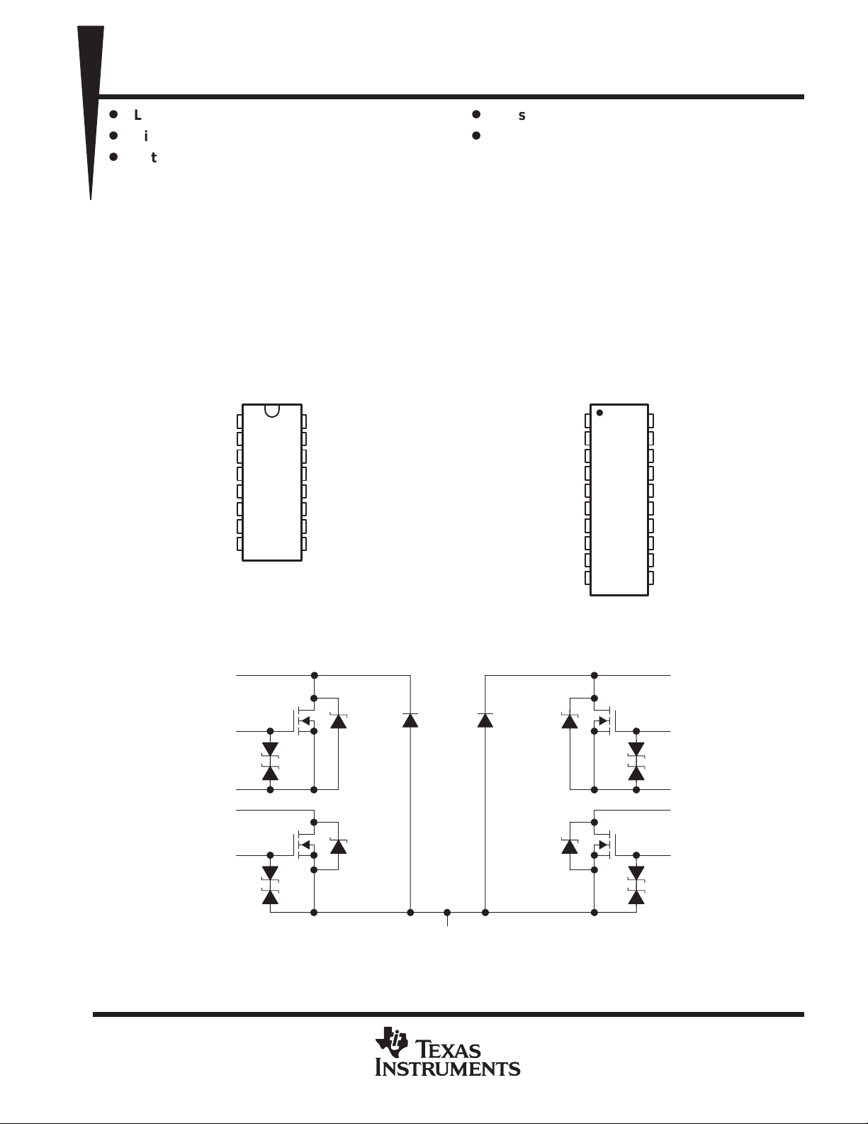
The TPIC5401 is a monolithic gate-protected power DMOS array that consists of four N-channel
enhancement-mode DMOS transistors, two of which are configured with a common source. Each transistor
features integrated high-current zener diodes (Z
overstress condition occurs. These zener diodes also provide up to 4000 V of ESD protection when tested using
the human-body model of a 100-pF capacitor in series with a 1.5-kΩ resistor.
The TPIC5401 is offered in a 16-pin thermally enhanced dual-in-line (NE) package and a 20-pin wide-body
surface-mount (DW) package and is characterized for operation over the case temperature range of –40°C to
125°C.
. . . 0.3 Ω Typ
NE PACKAGE
(TOP VIEW)
CXa
D
D
and Z
Pulsed Current...10 A Per Channel
Fast Commutation Speed
) to prevent gate damage in the event that an
CXb
DW PACKAGE
(TOP VIEW)
TPIC5401
SOURCE2/GND
SOURCE4/GND
schematic
DRAIN2
GATE2
GND
GND
GATE4
DRAIN4
DRAIN1
GATE1
SOURCE1
DRAIN2
Z
Z
C1b
C1a
16
15
14
13
12
11
10
9
Q1
Q2
SOURCE1
DRAIN1
GATE1
GND
GND
GATE3
DRAIN3
SOURCE3
D1
D2Z1 Z3
SOURCE4/GND
NC – No internal connection
1
2
3
4
5
6
7
8
GND
GATE4
NC
DRAIN4
SOURCE3
DRAIN3
GATE3
NC
NC
1
2
3
4
5
6
7
8
9
10
SOURCE2/GND
20
GATE2
19
NC
18
NC
17
DRAIN2
16
SOURCE1
15
14
DRAIN1
13
GATE1
12
NC
11
NC
Q3
Z
C3b
Z
C3a
Q4
DRAIN3
GATE3
SOURCE3
DRAIN4
GATE2
Z
C2b
Z
C2a
NOTE: For correct operation, no terminal pin may be taken below GND.
PRODUCTION DATA information is current as of publication date.
Products conform to specifications per the terms of Texas Instruments
standard warranty. Production processing does not necessarily include
testing of all parameters.
Z2 Z4
GND, SOURCE2, SOURCE4
POST OFFICE BOX 655303 • DALLAS, TEXAS 75265
GATE4
Z
C4b
Z
C4a
Copyright 1994, Texas Instruments Incorporated
1
Page 2

TPIC5401
H-BRIDGE GATE-PROTECTED
POWER DMOS ARRAY
SLIS024A – DECEMBER 1993 – REVISED MARCH 1994
absolute maximum ratings over operating case temperature range (unless otherwise noted)
Drain-to-source voltage, V
60 V. . . . . . . . . . . . . . . . . . . . . . . . . . . . . . . . . . . . . . . . . . . . . . . . . . . . . . . . . . . . . .
DS
†
Source-to-GND voltage (Q1, Q3) 100 V. . . . . . . . . . . . . . . . . . . . . . . . . . . . . . . . . . . . . . . . . . . . . . . . . . . . . . . . . . .
Drain-to-GND voltage (Q1, Q3) 100 V. . . . . . . . . . . . . . . . . . . . . . . . . . . . . . . . . . . . . . . . . . . . . . . . . . . . . . . . . . . . .
Drain-to-GND voltage (Q2, Q4) 60 V. . . . . . . . . . . . . . . . . . . . . . . . . . . . . . . . . . . . . . . . . . . . . . . . . . . . . . . . . . . . . .
Gate-to-source voltage range, V
Continuous drain current, each output, T
–9 V to 18 V. . . . . . . . . . . . . . . . . . . . . . . . . . . . . . . . . . . . . . . . . . . . . . . . . . .
GS
= 25°C: DW package 1.7 A. . . . . . . . . . . . . . . . . . . . . . . . . . . . . . . .
C
NE package 2 A. . . . . . . . . . . . . . . . . . . . . . . . . . . . . . . . . . .
Continuous source-to-drain diode current, T
Pulsed drain current, each output, I
max
Continuous gate-to-source zener-diode current, T
Pulsed gate-to-source zener-diode current, T
Single-pulse avalanche energy, E
, TC = 25°C (see Figures 4, 15, and 16) 21 mJ. . . . . . . . . . . . . . . . . . . . . .
AS
= 25°C 2 A. . . . . . . . . . . . . . . . . . . . . . . . . . . . . . . . . . . . . . . . . . . .
C
, TC = 25°C (see Note 1 and Figure 15) 10 A. . . . . . . . . . . . . . . . . . . .
= 25°C ±50 mA. . . . . . . . . . . . . . . . . . . . . . . . . . . . . . . . . .
C
= 25°C ±500 mA. . . . . . . . . . . . . . . . . . . . . . . . . . . . . . . . . . . . .
C
Continuous total dissipation See Dissipation Rating Table. . . . . . . . . . . . . . . . . . . . . . . . . . . . . . . . . . . . . . . . . . .
Operating virtual junction temperature range, T
Operating case temperature range, T
–40°C to 125°C. . . . . . . . . . . . . . . . . . . . . . . . . . . . . . . . . . . . . . . . . . . .
C
–40°C to 150°C. . . . . . . . . . . . . . . . . . . . . . . . . . . . . . . . . . . .
J
Storage temperature range, –65°C to 150°C. . . . . . . . . . . . . . . . . . . . . . . . . . . . . . . . . . . . . . . . . . . . . . . . . . . . .
Lead temperature 1,6 mm (1/16 inch) from case for 10 seconds 260°C. . . . . . . . . . . . . . . . . . . . . . . . . . . . . . .
†
Stresses beyond those listed under “absolute maximum ratings” may cause permanent damage to the device. These are stress ratings only, and
functional operation of the device at these or any other conditions beyond those indicated under “recommended operating conditions” is not
implied. Exposure to absolute-maximum-rated conditions for extended periods may affect device reliability.
NOTE 1: Pulse duration = 10 ms, duty cycle = 2%
DISSIPATION RATING TABLE
PACKAGE
DW
NE
TC ≤ 25°C
POWER RATING
1389 mW
2075 mW
DERATING FACTOR
ABOVE TC = 25°C
11.1 mW/°C
16.6 mW/°C
TC = 125°C
POWER RATING
279 mW
415 mW
2
POST OFFICE BOX 655303 • DALLAS, TEXAS 75265
Page 3
I
Zero-gate-voltage drain current
DS
,
A
I
Leakage current, drain-to-GND
V
V
A
r
Static drain-to-source on-state resistance
D
,
Ω
F
V
GS
g
di/dt
100 A/µs
See Figures 1 and 14
electrical characteristics, TC = 25°C (unless otherwise noted)
PARAMETER TEST CONDITIONS MIN TYP MAX UNIT
V
(BR)DSX
V
GS(th)
V
(BR)GS
V
(BR)SG
V
(BR)
V
DS(on)
V
F(SD)
V
F
DSS
I
GSSF
I
GSSR
lkg
DS(on)
g
fs
C
iss
C
oss
C
rss
NOTES: 2. Technique should limit TJ – TC to 10°C maximum.
Drain-to-source breakdown voltage ID = 250 µA, VGS = 0 60 V
Gate-to-source threshold voltage
Gate-to-source breakdown voltage IGS = 250 µA 18 V
Source-to-gate breakdown voltage ISG = 250 µA 9 V
Reverse drain-to-GND breakdown voltage
(across D1, D2)
Drain-to-source on-state voltage
Forward on-state voltage, source-to-drain
Forward on-state voltage, GND-to-drain
Forward-gate current, drain short circuited to source VGS = 15 V, VDS = 0 20 200 nA
Reverse-gate current, drain short circuited to source VSG = 5 V, VDS = 0 10 100 nA
Forward transconductance
Short-circuit input capacitance, common source 220 275
Short-circuit output capacitance, common source
Short-circuit reverse-transfer capacitance,
common source
3. These parameters are measured with voltage-sensing contacts separate from the current-carrying contacts.
ID = 1 mA,
See Figure 5
Drain-to-GND current = 250 µA 100 V
ID = 2 A,
See Notes 2 and 3
IS = 2 A,
VGS = 0 (Z1, Z2, Z3, Z4),
See Notes 2 and 3 and Figure 12
ID = 2 A (D1, D2),
See Notes 2 and 3
V
= 48 V,
VGS = 0
= 48
DGND
VGS = 10 V,
I
= 2 A,
See Notes 2 and 3
and Figures 6 and 7
VDS = 15 V, ID = 1 A,
See Notes 2 and 3 and Figure 9
VDS = 25 V, VGS = 0,
f = 1 MHz, See Figure 11
TPIC5401
H-BRIDGE GATE-PROTECTED
POWER DMOS ARRAY
SLIS024A – DECEMBER 1993 – REVISED MARCH 1994
VDS = V
VGS = 10 V,
TC = 25°C 0.05 1
TC = 125°C 0.5 10
TC = 25°C 0.05 1
TC = 125°C 0.5 10
TC = 25°C 0.3 0.35
TC = 125°C 0.47 0.5
GS,
1.5 1.85 2.2 V
0.6 0.7 V
1 1.2 V
7.5 V
1.6 1.9 S
120 150
100 125
µ
µ
p
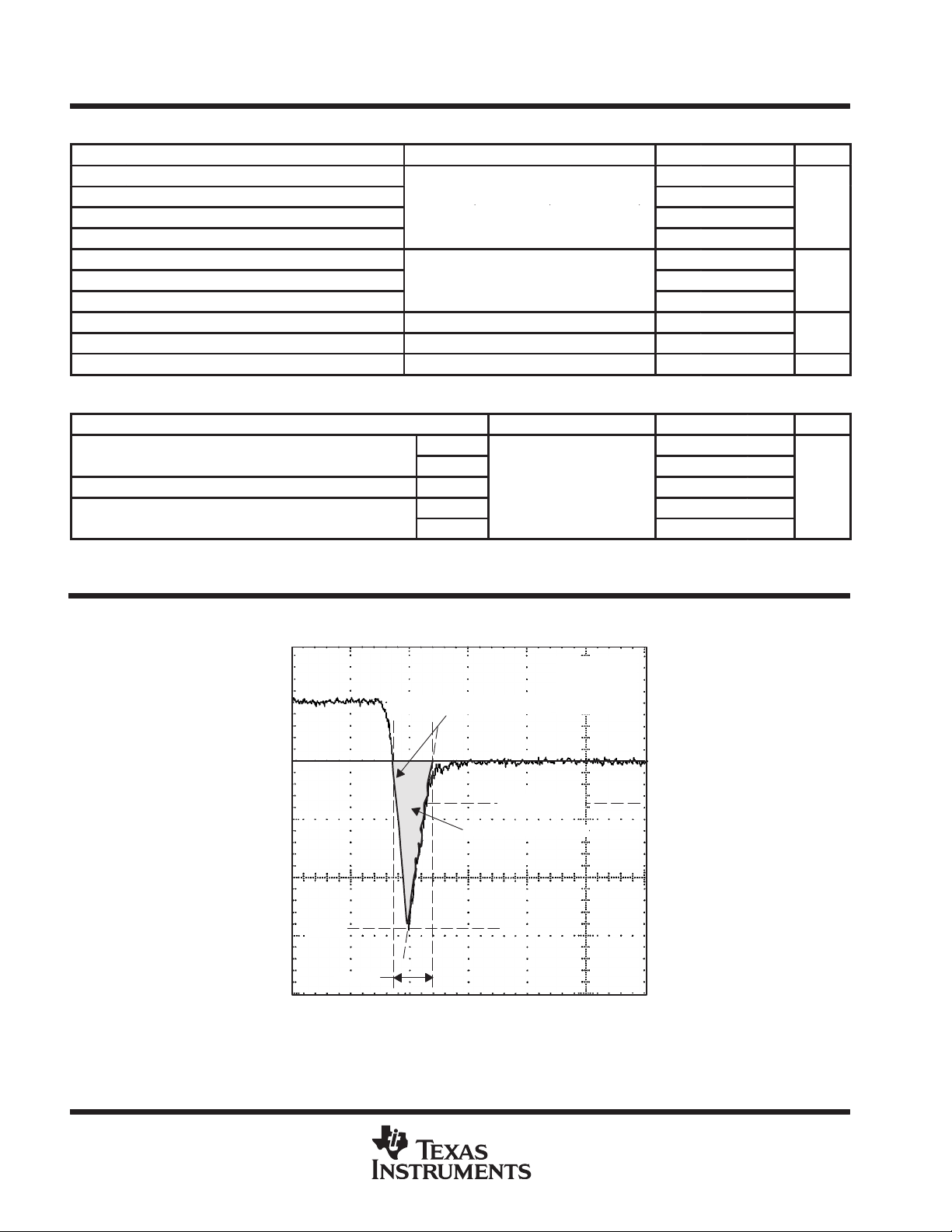
source-to-drain and GND-to-drain diode characteristics, TC = 25°C
PARAMETER TEST CONDITIONS MIN TYP MAX UNIT
t
rr
Q
Reverse-recovery time
Total diode charge
RR
IS = 1 A,
= 0,
See Fi
ures 1 and 14
POST OFFICE BOX 655303 • DALLAS, TEXAS 75265
VDS = 48 V,
=
Z1 and Z3 120
Z2 and Z4 280
D1 and D2 260
,
Z1 and Z3
Z2 and Z4 0.9
D1 and D2 2.2
ns
0.12
µC
3
Page 4
TPIC5401
DD
,
L
,
en
,
ns
See Figure 3
nH
R
Junction-to-ambient thermal resistance (see Note 4)
R
Junction-to-pin thermal resistance
H-BRIDGE GATE-PROTECTED
POWER DMOS ARRAY
SLIS024A – DECEMBER 1993 – REVISED MARCH 1994
resistive-load switching characteristics, TC = 25°C
PARAMETER TEST CONDITIONS MIN TYP MAX UNIT
t
d(on)
t
d(off)
t
r
t
f
Q
Q
Q
L
d
L
s
R
thermal resistances
R
NOTE 4: Package mounted on an FR4 printed-circuit board with no heatsink.
Turn-on delay time 32 65
Turn-off delay time
Rise time
Fall time 25 50
Total gate charge
g
Threshold gate-to-source charge
gs(th)
Gate-to-drain charge
gd
Internal drain inductance 5
Internal source inductance 5
Internal gate resistance 0.25 Ω
g
PARAMETER TEST CONDITIONS MIN TYP MAX UNIT
θJA
Junction-to-board thermal resistance DW
θJB
θJP
p
V
= 25 V, R
t
= 10 ns,
dis
VDS = 48 V,
DW 90
NE 60
DW 30
NE 25
= 25 Ω,t
See Figure 2
ID = 1 A, VGS = 10 V,
All outputs with equal power
= 10 ns,
40 80
15 30
6.6 8
0.8 1
2.6 3.2
53
nC
°C/W
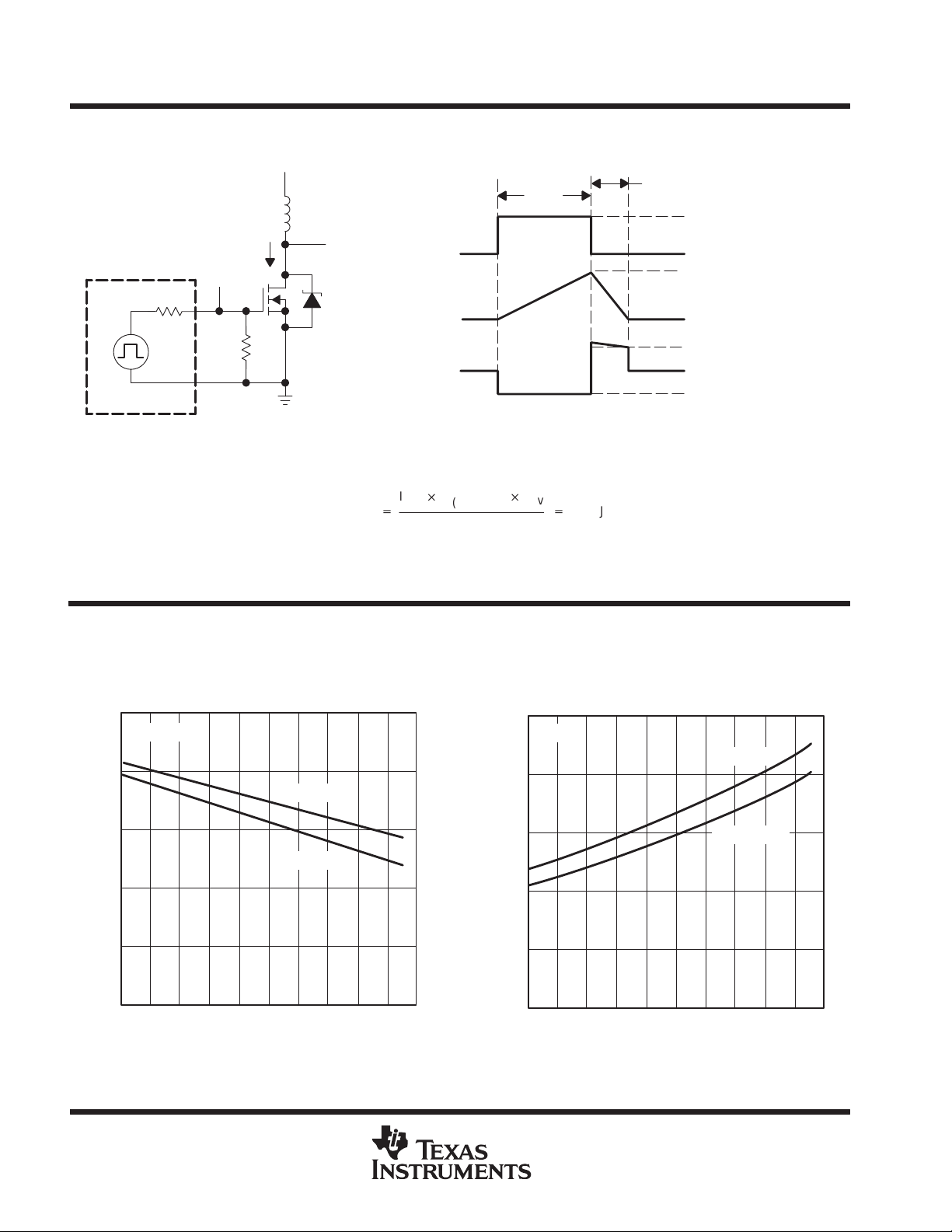
PARAMETER MEASUREMENT INFORMATION
2
1
0
– 1
– 2
– Source-to-Drain Diode Current – AI
S
– 3
– 4
0 200 400 600 800 1000 1200
†
IRM = maximum recovery current
‡
The above waveform is representative of Z2, Z4, D1, and D2 in shape only.
I
RM
†
t
rr(SD)
Reverse di/dt = 100 A/µs
25% of I
Shaded Area = Q
Time – ns
Figure 1. Reverse-Recovery-Current Waveform of Source-to-Drain Diode
VDS = 48 V
VGS = 0
TJ = 25°C
Z1 and Z3
†
RM
RR
‡
4
POST OFFICE BOX 655303 • DALLAS, TEXAS 75265
Page 5
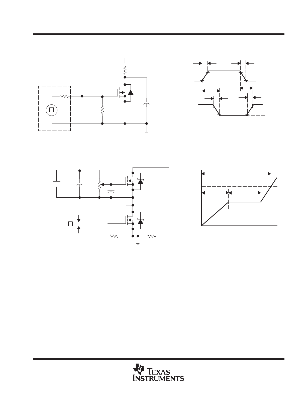
PARAMETER MEASUREMENT INFORMATION
Pulse Generator
R
gen
NOTE A: CL includes probe and jig capacitance.
50 Ω
V
GS
50 Ω
TEST CIRCUIT
Figure 2. Resistive-Switching Test Circuit and Voltage Waveforms
VDD = 25 V
R
L
DUT
V
DS
CL 30 pF
(see Note A)
H-BRIDGE GATE-PROTECTED
POWER DMOS ARRAY
SLIS024A – DECEMBER 1993 – REVISED MARCH 1994
t
en
V
GS
t
d(on)
t
f
V
DS
VOLTAGE WAVEFORMS
TPIC5401
t
dis
10 V
0 V
t
d(off)
t
r
V
DD
V
DS(on)
12-V
Battery
0 V
0.2 µF
50 kΩ
IG = 100 µA
IG Current-
Sampling Resistor
TEST CIRCUIT
Figure 3. Gate-Charge Test Circuit and Waveform
Current
Regulator
0.3 µF
V
DS
Same Type
as DUT
V
DD
DUT
ID Current-
Sampling Resistor
10 V
V
GS
Q
gs(th)
Q
g
Q
Gate Voltage
WAVEFORM
gd
Time
POST OFFICE BOX 655303 • DALLAS, TEXAS 75265
5
Page 6
TPIC5401
H-BRIDGE GATE-PROTECTED
POWER DMOS ARRAY
SLIS024A – DECEMBER 1993 – REVISED MARCH 1994
PARAMETER MEASUREMENT INFORMATION
VDD = 25 V
t
354 µH
V
V
Pulse Generator
(see Note A)
50 Ω
R
gen
TEST CIRCUIT
NOTES: A. The pulse generator has the following characteristics: tr ≤ 10 ns, tf ≤ 10 ns, ZO = 50 Ω.
B. Input pulse duration (tw) is increased until peak current IAS = 10 A.
Energy test level is defined as EAS+
V
GS
50 Ω
I
D
DS
DUT
IAS
GS
I
D
V
DS
V
(BR)DSX
2
Figure 4. Single-Pulse Avalanche-Energy Test Circuit and Waveforms
w
VOLTAGE AND CURRENT WAVEFORMS
t
av
+
21 mJ.
t
av
15 V
0 V
IAS (see Note B)
0 V
V
(BR)DSX
0 V
= 60 V Min
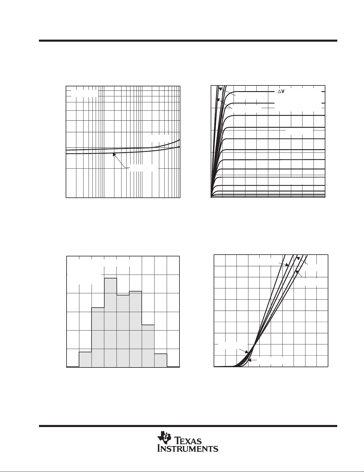
TYPICAL CHARACTERISTICS
GATE-TO-SOURCE THRESHOLD VOLTAGE
vs
JUNCTION TEMPERATURE
2.5
VDS = V
2
1.5
1
– Gate-to-Source Threshold Voltage – V
0.5
GS(th)
V
0
– 40 – 20 0 20 40 60 80 100 120 140 160
GS
ID = 1 mA
ID = 100 µA
TJ – Junction Temperature – °C
Figure 5
STATIC DRAIN-TO-SOURCE ON-STATE RESISTANCE
vs
JUNCTION TEMPERATURE
0.5
ID = 2 A
VGS = 10 V
0.4
Ω
0.3
0.2
– Static Drain-to-Sourcer
On-State Resistance –
DS(on)
0.1
0
– 40 – 20 0 20 40 60 80 100 120 140 160
TJ – Junction Temperature – °C
VGS = 15 V
Figure 6
6
POST OFFICE BOX 655303 • DALLAS, TEXAS 75265
Page 7
TPIC5401
H-BRIDGE GATE-PROTECTED
POWER DMOS ARRAY
SLIS024A – DECEMBER 1993 – REVISED MARCH 1994
TYPICAL CHARACTERISTICS
STATIC DRAIN-TO-SOURCE ON-STATE RESISTANCE
vs
DRAIN CURRENT
1
0.9
TJ = 25°C
0.8
0.7
0.6
Ω
0.5
0.4
VGS = 10 V
0.3
– Static Drain-to-Sourcer
0.2
On-State Resistance –
DS(on)
0.1
0.01 0.10 1 10
ID – Drain Current – A
VGS = 15 V
Figure 7
DISTRIBUTION OF
FORWARD TRANSCONDUCTANCE
30
Total Number of Units = 1040
VDS = 15 V
ID = 1 A
25
TJ = 25°C
20
DRAIN CURRENT
vs
DRAIN-TO-SOURCE VOLTAGE
5
VGS = 10 V
4
3
2
– Drain Current – A
D
I
1
0
VGS = 15 V
2468
VDS – Drain-to-Source Voltage – V
n
VGS = 0.2 V
TJ = 25°C
(unless otherwise
noted)
VGS = 4 V
VGS = 3 V
10 12 14 16 18 200
Figure 8
DRAIN CURRENT
vs
GATE-TO-SOURCE VOLTAGE
10
9
8
7
6
TJ = 25°C
T
= 75°C
J
TJ = 125°C
15
10
Percentage of Units – %
5
0
1.8
1.825
gfs – Forward Transconductance – S
1.85
1.875
Figure 9
1.9
5
4
– Drain Current – A
3
D
I
2
1
2
1.95
1.925
POST OFFICE BOX 655303 • DALLAS, TEXAS 75265
1.975
0
0
TJ = 150°C
TJ = –40°C
1234
VGS – Gate-to-Source Voltage – V
5678910
Figure 10
7
Page 8

TPIC5401
H-BRIDGE GATE-PROTECTED
POWER DMOS ARRAY
SLIS024A – DECEMBER 1993 – REVISED MARCH 1994
TYPICAL CHARACTERISTICS
CAPACITANCE
vs
DRAIN-TO-SOURCE VOLTAGE
500
f = 1 MHz
450
VGS = 0
TJ = 25°C
400
350
300
250
200
Capacitance – pF
150
100
50
0
010203040
VDS – Drain-to-Source Voltage – V
C
iss
C
oss
C
rss
Figure 11
DRAIN-TO-SOURCE VOLTAGE
AND GATE-TO-SOURCE VOLTAGE
vs
GATE CHARGE
60
ID = 1 A
TJ = 25°C
See Figure 3
50
VDD = 20 V
12
10
SOURCE-TO-DRAIN DIODE CURRENT
vs
SOURCE-TO-DRAIN VOLTAGE
10
VGS = 0
6
4
2
1
0.6
TJ = 125°C
0.4
– Source-to-Drain Diode Current – A
I
SD
TJ = 150°C
0.2
0.1
0.1 10
VSD – Source-to-Drain Voltage – V
1
TJ = –40°C
TJ = 25°C
TJ = 75°C
Figure 12
REVERSE-RECOVERY TIME
vs
REVERSE di/dt
400
350
300
VDS = 48 V
VGS = 0
IS = 1 A
TJ = 25°C
See Figure 1
– Drain-to-Source Voltage – V
DS
V
8
40
30
20
10
0
01234567
VDD = 30 V
VDD = 48 V
VDD = 20 V
Qg – Gate Charge – nC
Figure 13
POST OFFICE BOX 655303 • DALLAS, TEXAS 75265
8
6
4
2
0
– Reverse-Recovery Time – ns
– Gate-to-Source Voltage – V
rr
t
GS
V
250
200
150
100
50
0
0 100 200 300 400 500
Reverse di/dt – A/µs
Z2 and Z4
Z1 and Z3
Figure 14
600
Page 9

TPIC5401
H-BRIDGE GATE-PROTECTED
POWER DMOS ARRAY
SLIS024A – DECEMBER 1993 – REVISED MARCH 1994
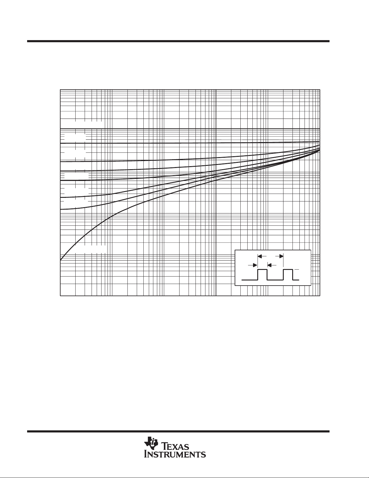
THERMAL INFORMATION
MAXIMUM DRAIN CURRENT
vs
DRAIN-TO-SOURCE VOLTAGE
100
TC = 25°C
10
†
10 ms
†
1 ms
†
1
– Maximum Drain Current – A
D
I
0.1
0.1 1 10 100
†
Less than 2% duty cycle
DW Pkg
DC Conditions
VDS – Drain-to-Source Voltage – V
500 µs
NE Pkg
Figure 15
1 µs
MAXIMUM PEAK-AVALANCHE CURRENT
vs
TIME DURATION OF AVALANCHE
30
See Figure 4
†
10
TC = 25°C
TC = 125°C
– Maximum Peak Avalanche Current – A
AS
I
1
0.01 0.1 1 10 100
tav – Time Duration of Avalanche – ms
Figure 16
POST OFFICE BOX 655303 • DALLAS, TEXAS 75265
9
Page 10
TPIC5401
H-BRIDGE GATE-PROTECTED
POWER DMOS ARRAY
SLIS024A – DECEMBER 1993 – REVISED MARCH 1994
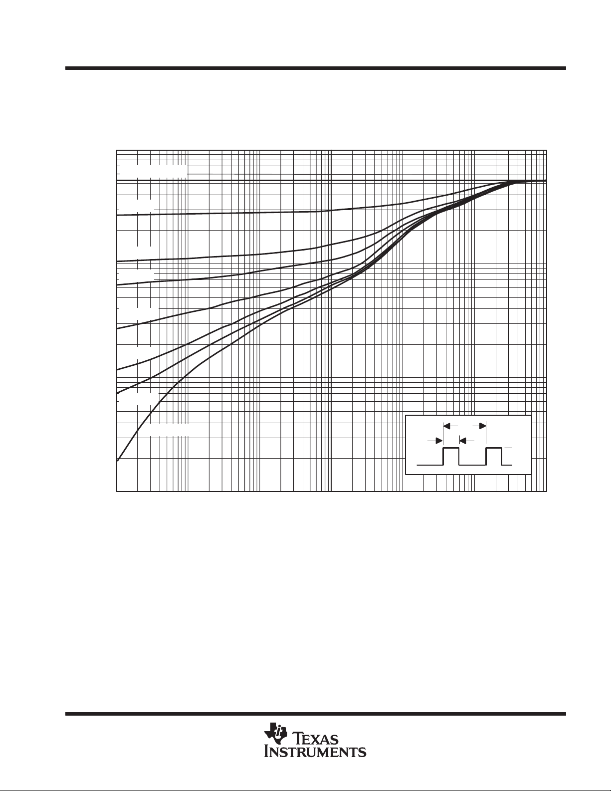
THERMAL INFORMATION
C/W
°
10
0.1
0.01
DC Conditions
1
d = 0.5
d = 0.2
d = 0.1
d = 0.05
d = 0.02
d = 0.01
NE PACKAGE
†
NORMALIZED JUNCTION-TO-AMBIENT THERMAL RESISTANCE
vs
PULSE DURATION
0.001
– Normalized Junction-to-Ambient Thermal Resistance –
JAθ
R
0.0001
0.0001 0.001
†
Device mounted on FR4 printed-circuit board with no heatsink.
NOTE A: Z
Single Pulse
(t) = r(t) R
θJA
tw = pulse duration
tc = cycle time
d = duty cycle = tw/t
θJA
0.01
c
tw – Pulse Duration – s
Figure 17
t
c
t
w
0.1 110
I
D
0
10
POST OFFICE BOX 655303 • DALLAS, TEXAS 75265
Page 11
TPIC5401
H-BRIDGE GATE-PROTECTED
POWER DMOS ARRAY
SLIS024A – DECEMBER 1993 – REVISED MARCH 1994
THERMAL INFORMATION
JUNCTION-TO-BOARD THERMAL RESISTANCE
100
DC Conditions
d = 0.5
C/W
°
d = 0.2
10
d = 0.1
d = 0.05
d = 0.02
1
– Junction-to-Board Thermal Resistance –
JBθ
R
d = 0.01
DW PACKAGE
†
vs
PULSE DURATION
Single Pulse
0.1
0.0001 0.001
†
Device mounted on 24 in2, 4-layer FR4 printed-circuit board with no heatsink.
NOTE B: Z
(t) = r(t) R
θJB
tw = pulse duration
tc = cycle time
d = duty cycle = tw/t
θJB
c
0.01 0.1 1 10
tw – Pulse Duration – s
Figure 18
t
c
t
w
I
D
0
POST OFFICE BOX 655303 • DALLAS, TEXAS 75265
11
Page 12

IMPORTANT NOTICE
T exas Instruments and its subsidiaries (TI) reserve the right to make changes to their products or to discontinue
any product or service without notice, and advise customers to obtain the latest version of relevant information
to verify, before placing orders, that information being relied on is current and complete. All products are sold
subject to the terms and conditions of sale supplied at the time of order acknowledgement, including those
pertaining to warranty, patent infringement, and limitation of liability.
TI warrants performance of its semiconductor products to the specifications applicable at the time of sale in
accordance with TI’s standard warranty. Testing and other quality control techniques are utilized to the extent
TI deems necessary to support this warranty . Specific testing of all parameters of each device is not necessarily
performed, except those mandated by government requirements.
CERT AIN APPLICATIONS USING SEMICONDUCTOR PRODUCTS MAY INVOLVE POTENTIAL RISKS OF
DEATH, PERSONAL INJURY, OR SEVERE PROPERTY OR ENVIRONMENTAL DAMAGE (“CRITICAL
APPLICATIONS”). TI SEMICONDUCTOR PRODUCTS ARE NOT DESIGNED, AUTHORIZED, OR
WARRANTED TO BE SUITABLE FOR USE IN LIFE-SUPPORT DEVICES OR SYSTEMS OR OTHER
CRITICAL APPLICA TIONS. INCLUSION OF TI PRODUCTS IN SUCH APPLICATIONS IS UNDERST OOD TO
BE FULLY AT THE CUSTOMER’S RISK.
In order to minimize risks associated with the customer’s applications, adequate design and operating
safeguards must be provided by the customer to minimize inherent or procedural hazards.
TI assumes no liability for applications assistance or customer product design. TI does not warrant or represent
that any license, either express or implied, is granted under any patent right, copyright, mask work right, or other
intellectual property right of TI covering or relating to any combination, machine, or process in which such
semiconductor products or services might be or are used. TI’s publication of information regarding any third
party’s products or services does not constitute TI’s approval, warranty or endorsement thereof.
Copyright 1998, Texas Instruments Incorporated
Page 13

WWW.ALLDATASHEET.COM
Copyright © Each Manufacturing Company.
All Datasheets cannot be modified without permission.
This datasheet has been download from :
www.AllDataSheet.com
100% Free DataSheet Search Site.
Free Download.
No Register.
Fast Search System.
www.AllDataSheet.com
 Loading...