

Page 1
TPIC5223L
2-CHANNEL INDEPENDENT GATE-PROTECTED LOGIC-LEVEL
POWER DMOS ARRAY
SLIS043A – NOVEMBER 1994 – REVISED SEPTEMBER 1995
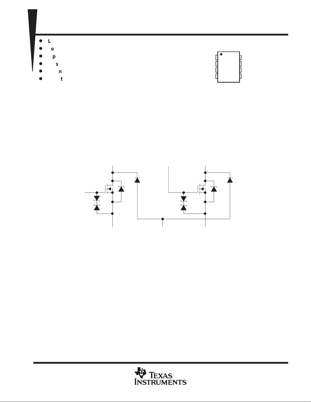
GND
D PACKAGE
(TOP VIEW)
1
2
3
4
8
7
6
5
DRAIN1
GATE1
SOURCE2
NC
D
Low r
DS(on)
D
Voltage Output...60 V
D
Input Protection Circuitry...18 V
D
Pulsed Current...3 A Per Channel
D
Extended ESD Capability...4000 V
D
Direct Logic-Level Interface
. . . 0.38 Ω Typ
description
SOURCE1
GATE2
DRAIN2
NC – No internal connection
The TPIC5223L is a monolithic gate-protected logic-level power DMOS array that consists of two electrically
isolated independent N-channel enhancement-mode DMOS transistors. Each transistor features integrated
high-current zener diodes (Z
CXa
and Z
) to prevent gate damage in the event that an overstress condition
CXb
occurs. These zener diodes also provide up to 4000 V of ESD protection when tested using the human-body
model of a 100-pF capacitor in series with a 1.5-kΩ resistor.
The TPIC5223L is offered in a standard eight-pin small-outline surface-mount (D) package and is characterized
for operation over the case temperature of –40°C to 125°C.
schematic
GATE1
Z
Z
7
C1b
C1a
DRAIN1
Q1
8
D1
Z1
GATE2
3
Z
Z
C2b
C2a
DRAIN2
Q2
4
D2
Z2
2
SOURCE1
NOTE A: For correct operation, no terminal may be taken below GND.
PRODUCTION DATA information is current as of publication date.
Products conform to specifications per the terms of Texas Instruments
standard warranty. Production processing does not necessarily include
testing of all parameters.
1 6
GND
SOURCE2
Copyright 1995, Texas Instruments Incorporated
POST OFFICE BOX 655303 • DALLAS, TEXAS 75265
1
Page 2

TPIC5223L
2-CHANNEL INDEPENDENT GATE-PROTECTED LOGIC-LEVEL
POWER DMOS ARRAY
SLIS043A – NOVEMBER 1994 – REVISED SEPTEMBER 1995
absolute maximum ratings over operating case temperature range (unless otherwise noted)
Drain-to-source voltage, V
60 V. . . . . . . . . . . . . . . . . . . . . . . . . . . . . . . . . . . . . . . . . . . . . . . . . . . . . . . . . . . . . .
DS
†
Source-to-GND voltage 100 V. . . . . . . . . . . . . . . . . . . . . . . . . . . . . . . . . . . . . . . . . . . . . . . . . . . . . . . . . . . . . . . . . . . .
Drain-to-GND voltage 100 V. . . . . . . . . . . . . . . . . . . . . . . . . . . . . . . . . . . . . . . . . . . . . . . . . . . . . . . . . . . . . . . . . . . . .
Gate-to-source voltage range, V
Continuous drain current, each output, T
Continuous source-to-drain diode current, T
Pulsed drain current, each output, I
Continuous gate-to-source zener diode current, T
Pulsed gate-to-source zener-diode current, T
Single-pulse avalanche energy, E
Continuous total power dissipation, T
Operating virtual junction temperature range, T
Operating case temperature range, T
Storage temperature range, T
–9 V to 18 V. . . . . . . . . . . . . . . . . . . . . . . . . . . . . . . . . . . . . . . . . . . . . . . . . . .
GS
max
AS
–65°C to 150°C. . . . . . . . . . . . . . . . . . . . . . . . . . . . . . . . . . . . . . . . . . . . . . . . . .
stg
= 25°C 1 A. . . . . . . . . . . . . . . . . . . . . . . . . . . . . . . . . . . . . . . . . . . . . . .
C
= 25°C 1 A. . . . . . . . . . . . . . . . . . . . . . . . . . . . . . . . . . . . . . . . . . . .
C
, TC = 25°C (see Note 1 and Figure 15) 3 A. . . . . . . . . . . . . . . . . . . . .
= 25°C ±50 mA. . . . . . . . . . . . . . . . . . . . . . . . . . . . . . . . . .
C
= 25°C ±500 mA. . . . . . . . . . . . . . . . . . . . . . . . . . . . . . . . . . . . .
C
, TC = 25°C (see Figures 4 and 16) 108 mJ. . . . . . . . . . . . . . . . . . . . . . .
= 25°C (see Figure 15) 0.95 W. . . . . . . . . . . . . . . . . . . . . . . . . . . . . . . . .
C
–40°C to 125°C. . . . . . . . . . . . . . . . . . . . . . . . . . . . . . . . . . . . . . . . . . . .
C
–40°C to 150°C. . . . . . . . . . . . . . . . . . . . . . . . . . . . . . . . . . . .
J
Lead temperature 1,6 mm (1/16 inch) from case for 10 seconds 260°C. . . . . . . . . . . . . . . . . . . . . . . . . . . . . . .
†
Stresses beyond those listed under “absolute maximum ratings” may cause permanent damage to the device. These are stress ratings only, and
functional operation of the device at these or any other conditions beyond those indicated under “recommended operating conditions” is not
implied. Exposure to absolute-maximum-rated conditions for extended periods may affect device reliability.
NOTE 1: Pulse duration = 10 ms, duty cycle = 2%
2
POST OFFICE BOX 655303 • DALLAS, TEXAS 75265
Page 3
I
Zero-gate-voltage drain current
DS
,
A
I
Leakage current, drain-to-GND
V
V
A
r
Static drain-to-source on-state resistance
D
,
Ω
F
trrReverse-recovery time
ns
V
GS
g
di/dt
100 A/µs
QRRTotal diode charge
See Figures 1 and 14
nC
2-CHANNEL INDEPENDENT GATE-PROTECTED LOGIC-LEVEL
SLIS043A – NOVEMBER 1994 – REVISED SEPTEMBER 1995
electrical characteristics, TC = 25°C (unless otherwise noted)
PARAMETER TEST CONDITIONS MIN TYP MAX UNIT
V
(BR)DSX
V
GS(th)
V
(BR)GS
V
(BR)SG
V
(BR)
V
DS(on)
V
F(SD)
V
F
DSS
I
GSSF
I
GSSR
lkg
DS(on)
g
fs
C
iss
C
oss
C
rss
NOTES: 2. Technique should limit TJ – TC to 10°C maximum.
Drain-to-source breakdown voltage ID = 250 µA, VGS = 0 60 V
Gate-to-source threshold voltage
Gate-to-source breakdown voltage IGS = 250 µA 18 V
Source-to-gate breakdown voltage ISG = 250 µA 9 V
Reverse drain-to-GND breakdown voltage
(across D1, D2)
Drain-to-source on-state voltage
Forward on-state voltage, source-to-drain
Forward on-state voltage, GND-to-drain
Forward-gate current, drain short circuited to source VGS = 15 V, VDS = 0 20 200 nA
Reverse-gate current, drain short circuited to source VSG = 5 V, VDS = 0 10 100 nA
Forward transconductance
Short-circuit input capacitance, common source 150 190
Short-circuit output capacitance, common source
Short-circuit reverse transfer capacitance,
common source
3. These parameters are measured with voltage-sensing contacts separate from the current-carrying contacts.
ID = 1 mA,
See Figure 5
Drain-to-GND current = 250 µA 100 V
ID = 1 A,
See Notes 2 and 3
IS = 1 A,
VGS = 0 (Z1, Z2),
See Notes 2 and 3 and Figure 12
ID = 1 A (D1, D2),
See Notes 2 and 3
V
= 48 V,
VGS = 0
= 48
DGND
VGS = 5 V,
I
= 1 A,
See Notes 2 and 3
and Figures 6 and 7
VDS = 15 V, ID = 500 mA,
See Notes 2 and 3 and Figure 9
VDS = 25 V, VGS = 0,
f = 1 MHz, See Figure 11
TPIC5223L
POWER DMOS ARRAY
VDS = V
VGS = 5 V,
TC = 25°C 0.05 1
TC = 125°C 0.5 10
TC = 25°C 0.05 1
TC = 125°C 0.5 10
TC = 25°C 0.38 0.43
TC = 125°C 0.61 0.65
GS,
1.5 2.05 2.2 V
0.375 0.425 V
0.85 1.2 V
3 V
1.2 1.49 S
100 125
40 50
µ
µ
p
source-to-drain and GND-to-drain diode characteristics, TC = 25°C
PARAMETER TEST CONDITIONS MIN TYP MAX UNIT
IS = 500 mA,
= 0,
See Fi
ures 1 and 14
POST OFFICE BOX 655303 • DALLAS, TEXAS 75265
VDS = 48 V,
=
Z1 and Z2 50
D1 and D2 210
,
Z1 and Z2
D1 and D2 800
50
3
Page 4
TPIC5223L
DD
,
L
,
r1
,
ns
See Figure 3
nH
2-CHANNEL INDEPENDENT GATE-PROTECTED LOGIC-LEVEL
POWER DMOS ARRAY
SLIS043A – NOVEMBER 1994 – REVISED SEPTEMBER 1995
resistive-load switching characteristics, TC = 25°C
PARAMETER TEST CONDITIONS MIN TYP MAX UNIT
t
d(on)
t
d(off)
t
r1
t
f2
Q
Q
Q
L
D
L
S
R
thermal resistance
R
R
R
NOTES: 4. Package mounted on an FR4 printed-circuit board with no heatsink.
Turn-on delay time 34 70
Turn-off delay time
Rise time
Fall time 15 30
Total gate charge
g
Threshold gate-to-source charge
gs(th)
Gate-to-drain charge
gd
Internal drain inductance 5
Internal source inductance 5
Internal gate resistance 0.25 Ω
g
PARAMETER TEST CONDITIONS MIN TYP MAX UNIT
Junction-to-ambient thermal resistance See Notes 4 and 7 130
θJA
Junction-to-board thermal resistance See Notes 5 and 7 78.6
θJB
Junction-to-pin thermal resistance See Notes 6 and 7 34
θJP
5. Package mounted on a 24 in2, 4-layer FR4 printed-circuit board.
6. Package mounted in intimate contact with infinite heatsink.
7. All outputs with equal power
V
= 25 V, R
tf1 = 10 ns,
VDS = 48 V,
= 50 Ω,t
See Figure 2
ID = 500 mA, VGS = 5 V,
= 10 ns,
20 40
28 55
3.1 3.8
0.5 0.6
1.9 2.3
nC
°C/W
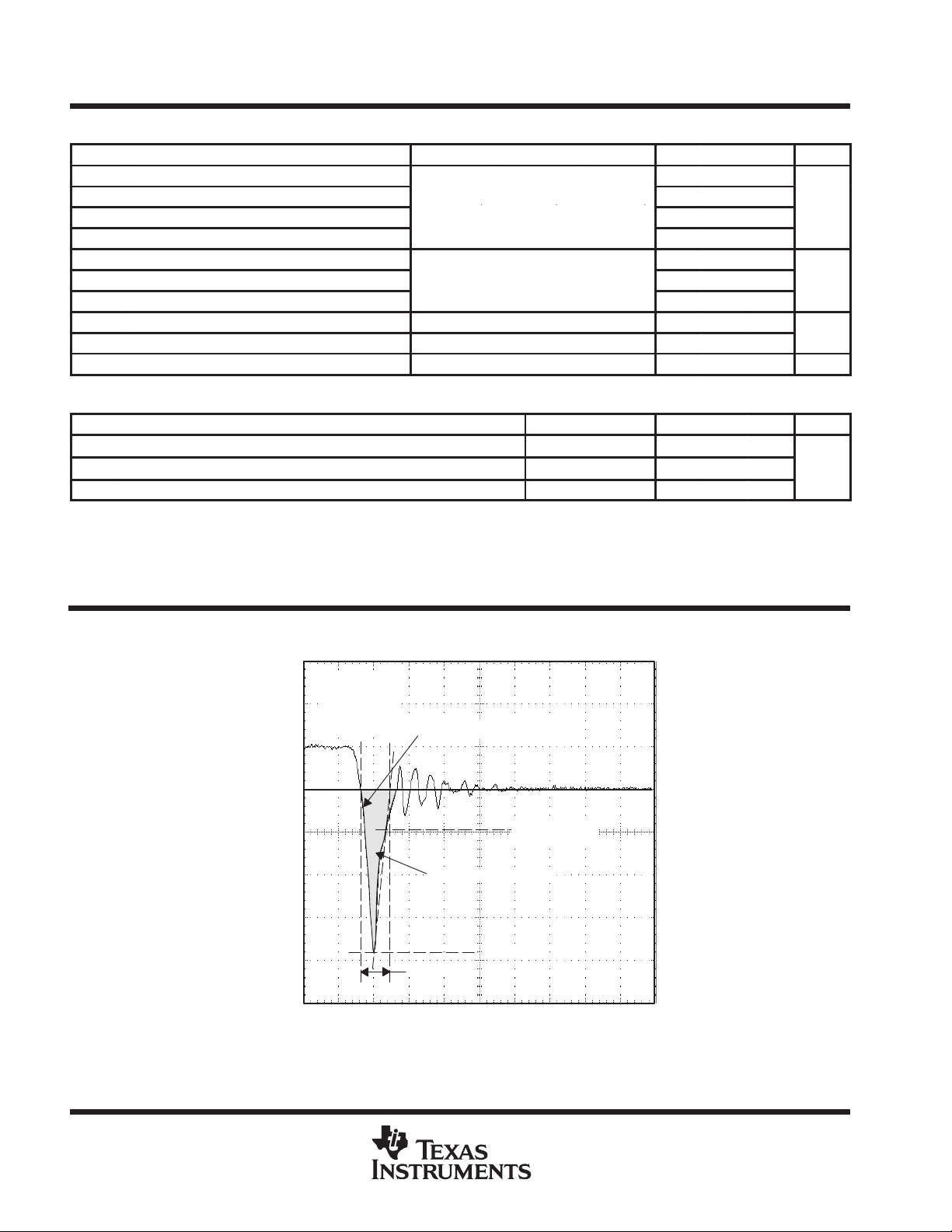
PARAMETER MEASUREMENT INFORMATION
1.5
VDS = 48 V
VGS = 0
1
TJ = 25°C
Z1, and Z2
0.5
0
– 0.5
– 1
– 1.5
– Source-to-Drain Diode Current – AI
S
– 2
– 2.5
0 50 100 150 200 250 300 350 400 450 500
†
IRM = maximum recovery current
‡
The above waveform is representative of D1 and D2 in shape only.
Figure 1. Reverse-Recovery-Current Waveform of Source-to-Drain Diode
‡
Reverse di/dt = 100 A/µs
Shaded Area = Q
I
t
rr(SD)
RM
Time – ns
25% of I
RR
†
RM
†
4
POST OFFICE BOX 655303 • DALLAS, TEXAS 75265
Page 5
TPIC5223L
2-CHANNEL INDEPENDENT GATE-PROTECTED LOGIC-LEVEL
POWER DMOS ARRAY
SLIS043A – NOVEMBER 1994 – REVISED SEPTEMBER 1995
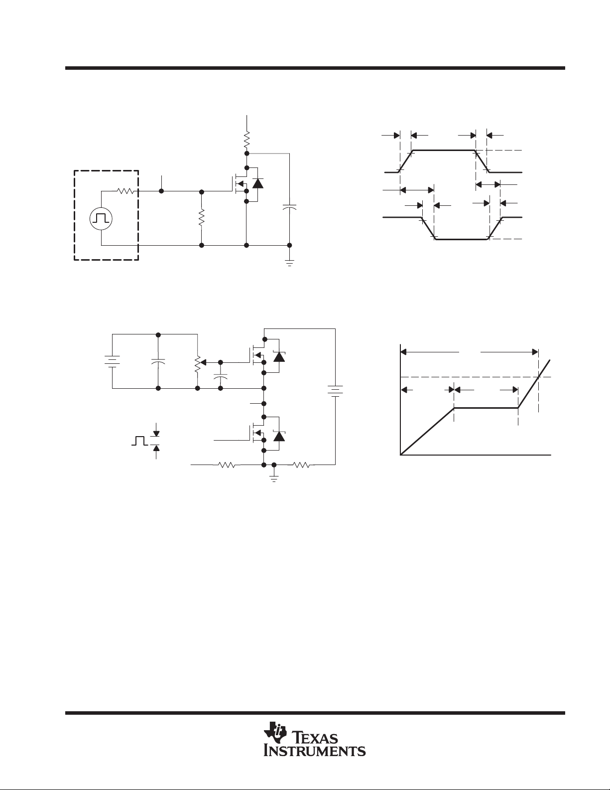
PARAMETER MEASUREMENT INFORMATION
VDD = 25 V
Pulse Generator
R
gen
NOTE A: CL includes probe and jig capacitance.
50 Ω
V
GS
50 Ω
TEST CIRCUIT
Figure 2. Resistive-Switching Test Circuit and Voltage Waveforms
Current
Regulator
12-V
Battery
0.2 µF
50 kΩ
0.3 µF
V
DS
t
V
t
d(on)
V
r1
GS
DS
t
f2
VOLTAGE WAVEFORMS
Q
g
5 V
Q
gs(th)
V
GS
R
L
V
DS
DUT
CL = 30 pF
(see Note A)
Same Type
as DUT
V
DD
t
f1
5 V
0 V
t
d(off)
t
r2
V
DD
V
DS(on)
Q
gd
0 V
IG = 100 µA
IG Current-
Sampling Resistor
TEST CIRCUIT
DUT
ID Current-
Sampling Resistor
Figure 3. Gate-Charge Test Circuit and Voltage Waveform
Gate Voltage
Time
VOLTAGE WAVEFORM
POST OFFICE BOX 655303 • DALLAS, TEXAS 75265
5
Page 6

TPIC5223L
2-CHANNEL INDEPENDENT GATE-PROTECTED LOGIC-LEVEL
POWER DMOS ARRAY
SLIS043A – NOVEMBER 1994 – REVISED SEPTEMBER 1995
PARAMETER MEASUREMENT INFORMATION
VDD = 25 V
t
14 mH
V
V
IAS
GS
I
DS
D
V
(BR)DSX
2
V
Pulse Generator
(see Note A)
50 Ω
R
gen
NOTES: A. The pulse generator has the following characteristics: tr ≤ 10 ns, tf ≤ 10 ns, ZO = 50 Ω.
TEST CIRCUIT
B. Input pulse duration (tw) is increased until peak current IAS = 3 A.
Energy test level is defined as EAS+
V
GS
50 Ω
I
D
DS
DUT
Figure 4. Single-Pulse Avalanche-Energy Test Circuit and Waveforms
w
VOLTAGE AND CURRENT WAVEFORMS
t
av
+
108 mJ, where tav+
t
av
5 V
0 V
I
AS
(see Note B)
0 V
V
(BR)DSX
0 V
avalanche time.
= 60 V Min
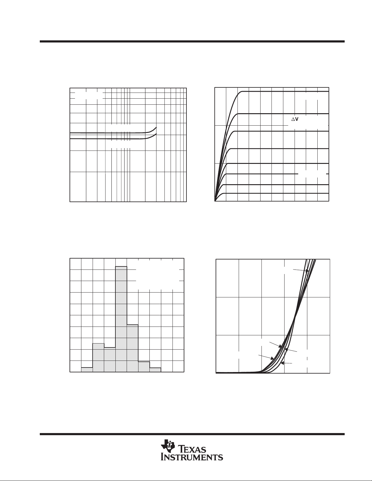
TYPICAL CHARACTERISTICS
GATE-TO-SOURCE THRESHOLD VOLTAGE
vs
JUNCTION TEMPERATURE
2.5
2
ID = 100 µA
1.5
1
– Gate-to-Source Threshold Voltage – V
0.5
GS(th)
V
0
–40 –20 0 20 40 60 80 100 120 140 160
TJ – Junction Temperature – °C
Figure 5
VDS = V
ID = 1 mA
GS
STATIC DRAIN-TO-SOURCE ON-STATE RESISTANCE
vs
JUNCTION TEMPERATURE
1
ID = 1 A
0.8
Ω
0.6
VGS = 4.5 V
0.4
– Static Drain-to-Source
On-State Resistance –
DS(on)
r
0.2
0
–40 –20 0 20 40 60 80 100 120 140 160
VGS = 5 V
TJ – Junction Temperature – °C
Figure 6
6
POST OFFICE BOX 655303 • DALLAS, TEXAS 75265
Page 7
TPIC5223L
2-CHANNEL INDEPENDENT GATE-PROTECTED LOGIC-LEVEL
POWER DMOS ARRAY
SLIS043A – NOVEMBER 1994 – REVISED SEPTEMBER 1995
TYPICAL CHARACTERISTICS
STATIC DRAIN-TO-SOURCE ON-STATE RESISTANCE
vs
DRAIN CURRENT
1
0.9
TJ = 25°C
0.8
0.7
0.6
Ω
0.5
0.4
0.3
– Static Drain-to-Sourcer
On-State Resistance –
DS(on)
0.2
0.1
VGS = 4.5 V
VGS = 5 V
1
ID – Drain Current – A
Figure 7 Figure 8
DISTRIBUTION OF
50
45
40
35
30
FORWARD TRANSCONDUCTANCE
Total Number
of Units = 1554
VDS = 15 V
ID = 500 mA
TJ = 25°C
10
DRAIN CURRENT
vs
DRAIN-TO-SOURCE VOLTAGE
3
VGS = 4 V
n
VGS = 0.2 V
2
– Drain Current – A
1
D
I
0
12345678910
VDS – Drain-to-Source Voltage – V
TJ = 25°C
VGS = 3 V
DRAIN CURRENT
vs
GATE-TO-SOURCE VOLTAGE
3
T
= 75°C
J
2
25
20
15
Percentage of Units – %
10
5
0
1.470
1.475
1.480
gfs – Forward Transconductance – S
– Drain Current – A
1
1.485
1.490
1.495
1.500
1.505
1.510
1.515
D
I
0
012345
TJ = 125°C
TJ = 150°C
VGS – Gate-to-Source Voltage – V
Figure 9 Figure 10
POST OFFICE BOX 655303 • DALLAS, TEXAS 75265
TJ = 25°C
TJ = –40°C
7
Page 8
TPIC5223L
2-CHANNEL INDEPENDENT GATE-PROTECTED LOGIC-LEVEL
POWER DMOS ARRAY
SLIS043A – NOVEMBER 1994 – REVISED SEPTEMBER 1995
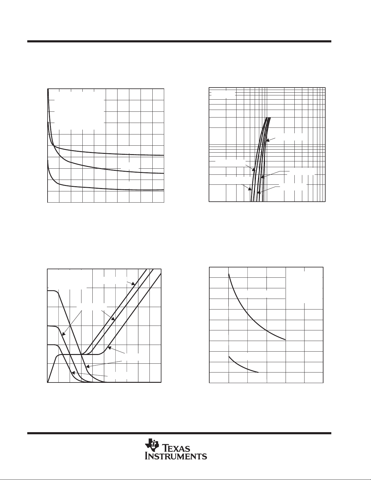
TYPICAL CHARACTERISTICS
DRAIN-TO-SOURCE VOLTAGE
350
315
280
245
210
175
140
C – Capacitance – pF
105
VGS = 0
f = 1 MHz
TJ = 25°C
C
= 245 pF
iss(0)
C
oss(0)
C
= 132 pF
rss(0)
70
35
0
0481216
VDS – Drain-to-Source Voltage – V
DRAIN-TO-SOURCE VOLTAGE AND
GATE-TO-SOURCE VOLTAGE
60
ID = 500 mA
TJ = 25°C
See Figure 3
50
40
CAPACITANCE
= 3700 pF
Figure 11
vs
GATE CHARGE
VDD = 20 V
VDD = 30 V
vs
C
iss
C
oss
C
rss
20 24 28 32 36
40
12
10
8
SOURCE-TO-DRAIN DIODE CURRENT
vs
SOURCE-TO-DRAIN VOLTAGE
10
VGS = 0
TJ = –40°C
1
TJ = 125°C
TJ = 25°C
– Source-to-Drain Diode Current – A
SD
I
0.1
0.1 10
TJ = 150°C
TJ = 75°C
1
VSD – Source-to-Drain Voltage – V
Figure 12
REVERSE-RECOVERY TIME
vs
REVERSE di/dt
220
200
180
D1 and D2
160
140
VDS = 48 V
VGS = 0
IS = 500 mA
TJ = 25°C
See Figure 1
– Drain-to-Source Voltage – V
DS
V
8
30
20
10
VDD = 20 V
0
0 0.5 1 1.5 2 2.5 3 3.5
Qg – Gate Charge – nC
Figure 13 Figure 14
6
4
– Reverse-Recovery Time – ns
2
0
– Gate-to-Source Voltage – V
t
GS
V
rr
VDD = 48 V
4 4.5 5
POST OFFICE BOX 655303 • DALLAS, TEXAS 75265
120
100
80
60
40
20
0
0 100 200 300
Z1 and Z2
400
Reverse di/dt – A/µs
500 600
Page 9

TPIC5223L
2-CHANNEL INDEPENDENT GATE-PROTECTED LOGIC-LEVEL
POWER DMOS ARRAY
SLIS043A – NOVEMBER 1994 – REVISED SEPTEMBER 1995
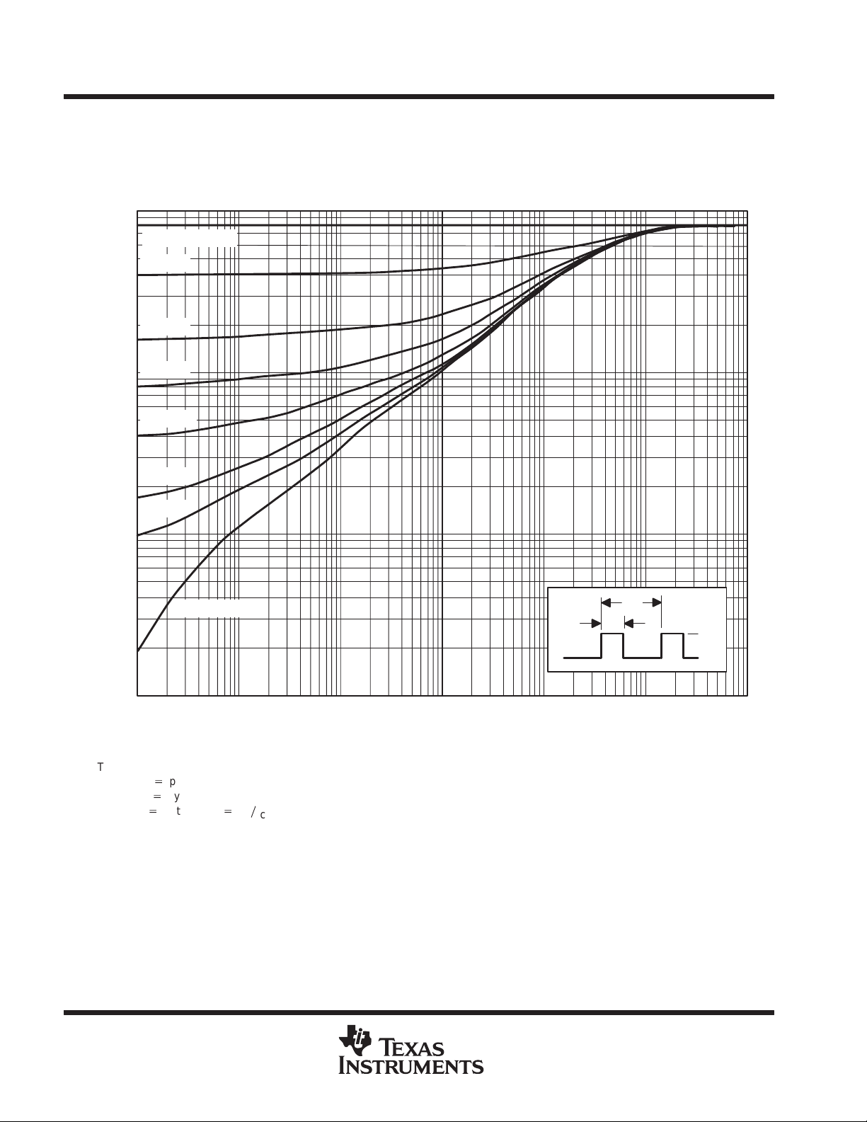
THERMAL INFORMATION
MAXIMUM DRAIN CURRENT
vs
DRAIN-TO-SOURCE VOLTAGE
10
TC = 25°C
†
1 µs
†
1 ms
†
10 ms
1
§
– Maximum Drain Current – A
D
I
DC Conditions
0.1
0.1 1 10 100
†
Less than 2% duty cycle
‡
Device mounted in intimate contact with infinite heatsink.
§
Device mounted on FR4 printed-circuit board with no heatsink.
VDS – Drain-to-Source Voltage – V
θJA
500 µs
θJP
†
‡
Figure 15
MAXIMUM PEAK AVALANCHE CURRENT
TIME DURATION OF AVALANCHE
5
See Figure 4
4
3
TC = 125°C
2
– Maximum Peak Avalanche Current – A
AS
I
1
0.01 0.1 1
tav – Time Duration of Avalanche – ms
vs
TC = 25°C
10 100
Figure 16
POST OFFICE BOX 655303 • DALLAS, TEXAS 75265
9
Page 10
TPIC5223L
2-CHANNEL INDEPENDENT GATE-PROTECTED LOGIC-LEVEL
POWER DMOS ARRAY
SLIS043A – NOVEMBER 1994 – REVISED SEPTEMBER 1995
THERMAL INFORMATION
JUNCTION-TO-BOARD THERMAL RESISTANCE
100
DC Conditions
d = 0.5
C/W
°
– Junction-to-Board Thermal Resistance –
JBθ
R
10
d = 0.2
d = 0.1
d = 0.05
d = 0.02
d = 0.01
1
Single Pulse
D PACKAGE
†
vs
PULSE DURATION
t
c
t
w
I
D
0
0.1
0.0001 0.001
†
Device mounted on 24 in2, 4-layer FR4 printed-circuit board with no heatsink.
NOTE A: ZθB(t) = r(t) R
tw+
tc+
d+duty cycle+twń
θJB
pulse duration
cycle time
t
c
0.01 0.1 1 10
tw – Pulse Duration – s
Figure 17
10
POST OFFICE BOX 655303 • DALLAS, TEXAS 75265
100
Page 11

PACKAGE OPTION ADDENDUM
www.ti.com
8-Apr-2005
PACKAGING INFORMATION
Orderable Device Status
(1)
Package
Type
Package
Drawing
Pins Package
Qty
Eco Plan
TPIC5223LD OBSOLETE SOIC D 8 TBD Call TI Call TI
(1)
The marketing status values are defined as follows:
ACTIVE: Product device recommended for new designs.
LIFEBUY: TI has announced that the device will be discontinued, and a lifetime-buy period is in effect.
NRND: Not recommended for new designs. Device is in production to support existing customers, but TI does not recommend using this part in
a new design.
PREVIEW: Device has been announced but is not in production. Samples may or may not be available.
OBSOLETE: TI has discontinued the production of the device.
(2)
Eco Plan - The planned eco-friendly classification: Pb-Free (RoHS) or Green (RoHS & no Sb/Br) - please check
http://www.ti.com/productcontent for the latest availability information and additional product content details.
TBD: The Pb-Free/Green conversion plan has not been defined.
Pb-Free (RoHS): TI's terms "Lead-Free" or "Pb-Free" mean semiconductor products that are compatible with the current RoHS requirements
for all 6 substances, including the requirement that lead not exceed 0.1% by weight in homogeneous materials. Where designed to be soldered
at high temperatures, TI Pb-Free products are suitable for use in specified lead-free processes.
Green (RoHS & no Sb/Br): TI defines "Green" to mean Pb-Free (RoHS compatible), and free of Bromine (Br) and Antimony (Sb) based flame
retardants (Br or Sb do not exceed 0.1% by weight in homogeneous material)
(3)
MSL, Peak Temp. -- The Moisture Sensitivity Level rating according to the JEDEC industry standard classifications, and peak solder
temperature.
(2)
Lead/Ball Finish MSL Peak Temp
(3)
Important Information and Disclaimer:The information provided on this page represents TI's knowledge and belief as of the date that it is
provided. TI bases its knowledge and belief on information provided by third parties, and makes no representation or warranty as to the
accuracy of such information. Efforts are underway to better integrate information from third parties. TI has taken and continues to take
reasonable steps to provide representative and accurate information but may not have conducted destructive testing or chemical analysis on
incoming materials and chemicals. TI and TI suppliers consider certain information to be proprietary, and thus CAS numbers and other limited
information may not be available for release.
In no event shall TI's liability arising out of such information exceed the total purchase price of the TI part(s) at issue in this document sold by TI
to Customer on an annual basis.
Addendum-Page 1
Page 12

Page 13

IMPORTANT NOTICE
Texas Instruments Incorporated and its subsidiaries (TI) reserve the right to make corrections, modifications,
enhancements, improvements, and other changes to its products and services at any time and to discontinue
any product or service without notice. Customers should obtain the latest relevant information before placing
orders and should verify that such information is current and complete. All products are sold subject to TI’s terms
and conditions of sale supplied at the time of order acknowledgment.
TI warrants performance of its hardware products to the specifications applicable at the time of sale in
accordance with TI’s standard warranty. Testing and other quality control techniques are used to the extent TI
deems necessary to support this warranty . Except where mandated by government requirements, testing of all
parameters of each product is not necessarily performed.
TI assumes no liability for applications assistance or customer product design. Customers are responsible for
their products and applications using TI components. To minimize the risks associated with customer products
and applications, customers should provide adequate design and operating safeguards.
TI does not warrant or represent that any license, either express or implied, is granted under any TI patent right,
copyright, mask work right, or other TI intellectual property right relating to any combination, machine, or process
in which TI products or services are used. Information published by TI regarding third-party products or services
does not constitute a license from TI to use such products or services or a warranty or endorsement thereof.
Use of such information may require a license from a third party under the patents or other intellectual property
of the third party, or a license from TI under the patents or other intellectual property of TI.
Reproduction of information in TI data books or data sheets is permissible only if reproduction is without
alteration and is accompanied by all associated warranties, conditions, limitations, and notices. Reproduction
of this information with alteration is an unfair and deceptive business practice. TI is not responsible or liable for
such altered documentation.
Resale of TI products or services with statements different from or beyond the parameters stated by TI for that
product or service voids all express and any implied warranties for the associated TI product or service and
is an unfair and deceptive business practice. TI is not responsible or liable for any such statements.
Following are URLs where you can obtain information on other Texas Instruments products and application
solutions:
Products Applications
Amplifiers amplifier.ti.com Audio www.ti.com/audio
Data Converters dataconverter.ti.com Automotive www.ti.com/automotive
DSP dsp.ti.com Broadband www.ti.com/broadband
Interface interface.ti.com Digital Control www.ti.com/digitalcontrol
Logic logic.ti.com Military www.ti.com/military
Power Mgmt power.ti.com Optical Networking www.ti.com/opticalnetwork
Microcontrollers microcontroller.ti.com Security www.ti.com/security
Low Power Wireless www.ti.com/lpw Telephony www.ti.com/telephony
Video & Imaging www.ti.com/video
Wireless www.ti.com/wireless
Mailing Address: Texas Instruments
Post Office Box 655303 Dallas, Texas 75265
Copyright 2006, Texas Instruments Incorporated
 Loading...