

TPIC46L01, TPIC46L02, TPIC46L03
6-CHANNEL SERIAL AND PARALLEL LOW-SIDE PRE-FET DRIVER
SLIS055A – NOVEMBER 1996 - REVISED SEPTEMBER 1997
D
6-Channel Serial-in/Parallel-in Low-side
Pre-FET Driver
D
Device Can Be Cascaded
D
Internal 55-V Inductive Load Clamp and
V
Protection Clamp for External Power
GS
FETs
D
Independent Shorted-Load/Short-to-Battery
Fault Detection on All Drain Terminals
D
Independent Off-State Open-Load Fault
Sense
D
Over-Battery-Voltage Lockout Protection
and Fault Reporting
D
Under-Battery-Voltage Lockout Protection
for TPIC46L01 and TPIC46L02
D
Asynchronous Open-Drain Fault Flag
D
Device Output Can be Wire-ORed with
Multiple External Devices
D
Fault Status Returned Through Serial
Output Terminal
D
Internal Global Power-on Reset of Device
D
High-Impedance CMOS Compatible Inputs
With Hysteresis
D
TPIC46L01 and TPIC46L03 Disables the
Gate Output When a Shorted-Load Fault
Occurs
D
TPIC46L02 Transitions the Gate Output to a
Low-Duty-Cycle PWM Mode When a
Shorted-Load Fault Occurs
description
FL T
IN0
IN1
IN2
IN3
IN4
IN5
CS
SDO
SDI
SCLK
V
CC
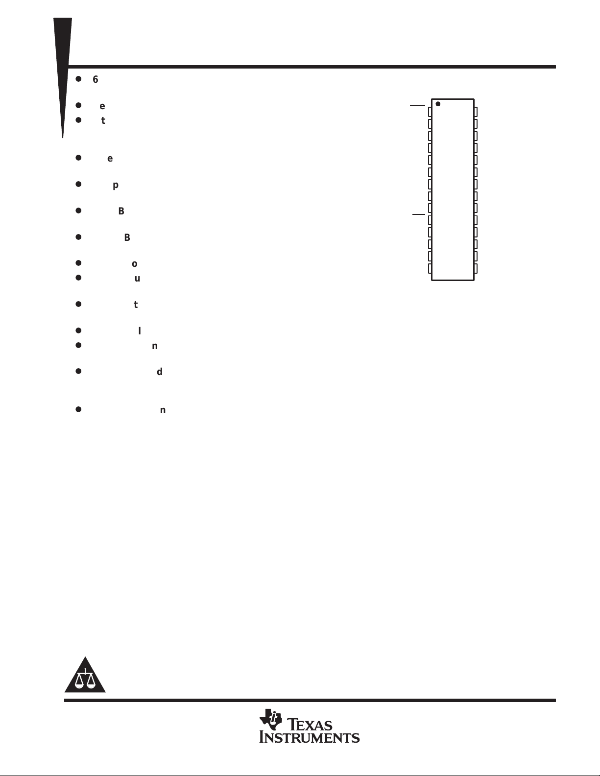
DB PACKAGE
(TOP VIEW)
1
28
2
27
3
26
4
25
5
24
6
23
7
22
8
21
9
20
10
19
11
18
12
17
13
16
14
15
V
BAT
GATE0
DRAIN0
GATE1
DRAIN1
DRAIN2
GATE2
GATE3
DRAIN3
DRAIN4
GATE4
DRAIN5
GATE5
GND
VCOMPEN
VCOMP
The TPIC46L01, TPIC46L02, and TPIC46L03 are low-side predrivers that provide serial input interface and
parallel input interface to control six external field-effect transistor(FET) power switches such as offered in the
TI TPIC family of power arrays. These devices are designed primarily for low-frequency switching, inductive
load applications such as solenoids and relays. Fault status for each channel is available in a serial-data format.
Each driver channel has independent off-state open-load detection and on-state shorted-load/short-to-battery
detection. Battery overvoltage and undervoltage detection and shutdown are provided. Battery and output load
faults provide real-time fault reporting to the controller. Each channel also provides inductive-voltage-transient
protection for the external FET.
These devices provide control of output channels through a serial input interface or a parallel input interface.
A command to enable the output from either interface enables the respective channel GATE output to the
external FET . The serial input interface is recommended when the number of signals between the control device
and the predriver must be minimized, and the speed of operation is not critical. In applications where the
predriver must respond very quickly or asynchronously, the parallel input interface is recommended.
Please be aware that an important notice concerning availability, standard warranty, and use in critical applications of
Texas Instruments semiconductor products and disclaimers thereto appears at the end of this data sheet.
PRODUCTION DATA information is current as of publication date.
Products conform to specifications per the terms of Texas Instruments
standard warranty. Production processing does not necessarily include
testing of all parameters.
POST OFFICE BOX 655303 • DALLAS, TEXAS 75265
Copyright 1997, Texas Instruments Incorporated
1

TPIC46L01, TPIC46L02, TPIC46L03
6-CHANNEL SERIAL AND PARALLEL LOW-SIDE PRE-FET DRIVER
SLIS055A – NOVEMBER 1996 - REVISED SEPTEMBER 1997
For serial operation, the control device must transition CS from high to low to activate the serial input interface.
When this occurs, SDO is enabled, fault data is latched into the serial input interface, and the FLT
refreshed.
Data is clocked into the serial registers on low-to-high transitions of SCLK through SDI. Each string of data must
consist of 8 bits of data. In applications where multiple devices are cascaded together, the string of data must
consist of 8 bits for each device. A high data bit turns the respective output channel on and a low data bit turns
it off. Fault data for the device is clocked out of SDO as serial input data is clocked into the device. Fault data
consists of fault flags for the over-battery voltage (bit 8), under-battery voltage (bit 7) (not on TPIC46L03) and
shorted/open-load flags (bits 1-6) for each of the six output channels. A logic-high bit in the fault data indicates
a fault and a logic-low bit indicates that no fault is present on that channel. Fault register bits are set or cleared
asynchronously to reflect the current state of the hardware. The fault must be present when CS
from high to low to be captured and reported in the serial fault data. New faults cannot be captured in the serial
register when CS
A low-to-high transition of CS
high-impedance state, and clears and re-enables the fault register. The TPIC46L01/L02/L03 was designed to
allow the serial input interfaces of multiple devices to be cascaded together to simplify the serial interface to the
controller. Serial input data flows through the device and is transferred out SDO following the fault data in
cascaded configurations.
For parallel operation, data is asynchronously transferred directly from the parallel input interface (IN0-IN5) to
the respective GA TE output. SCLK or CS
respective channel on, where a 0 turns it off. Note that either the serial interface or the parallel interface can
enable a channel. Under parallel operation, fault data must still be collected through the serial data interface.
is low. CS must be transitioned high after all of the serial data has been clocked into the device.
transfers the last six bits of serial data to the output buffer, puts SDO in a
are not required for parallel control. A 1 on the parallel input turns the
is transitioned
flag is
The predrivers monitor the drain voltage for each channel to detect shorted-load or open-load fault conditions
in the on and off states respectively. These devices offer the option of using an internally generated
fault-reference voltage or an externally supplied VCOMP for fault detection. The internal fault reference is
selected by connecting VCOMPEN
to V
shorted-load conditions and when the channel is off to detect open-load conditions. When a shorted-load fault
occurs using the TPIC46L01 or TPIC46L03, the channel is turned off and a fault signal is sent to FLT
as to the serial fault-register bit. When a shorted-load fault occurs while using the TPIC46L02, the channel
transitions into a low-duty-cycle, pulse-width-modulated (PWM) signal as long as the fault is present.
Shorted-load conditions must be present for at least the shorted-load deglitch time, t
flagged as a fault. A fault signal is sent to FL T
operation is presented in the device operation section of this data sheet.
The TPIC46L01 and TPIC46L02 provide protection from over-battery voltage and under-battery voltage
conditions irrespective of the state of the output channels. The TPIC46L03 provides protection from over-battery
voltage conditions irrespective of the state of the output channels When the battery voltage is greater than the
overvoltage threshold or less than the undervoltage threshold (except for the TPIC46L03, which has no
undervoltage threshold), all channels are disabled and a fault signal is sent to FL T
fault register bits. The outputs return to normal operation once the battery voltage fault has been corrected.
When an over-battery/under-battery voltage condition occurs, the device reports the battery fault, but disables
fault reporting for open and shorted-load conditions. Fault reporting for open and shorted-load conditions are
re-enabled after the battery fault condition has been corrected.
These devices provide inductive transient protection on all channels. The drain voltage is clamped to protect
the FET . This clamp voltage is defined by the sum of V
also provides a gate-to-source voltage (V
exceeding their rated voltages.
. The drain voltage is compared to the fault-reference voltage when the channel is turned on to detect
CC
to GND and the external reference is selected by connecting VCOMPEN
as well
as well as the serial fault register bit. More detail on fault detection
and turn-on voltage of the external FET . The predriver
) clamp to protect the GA TE-source terminals of the power FET from
GS
C
(STBDG)
as well as to the respective
, in order to be
These devices provide pulldown resistors on all inputs except CS
2
POST OFFICE BOX 655303 • DALLAS, TEXAS 75265
. A pullup resistor is used on CS.
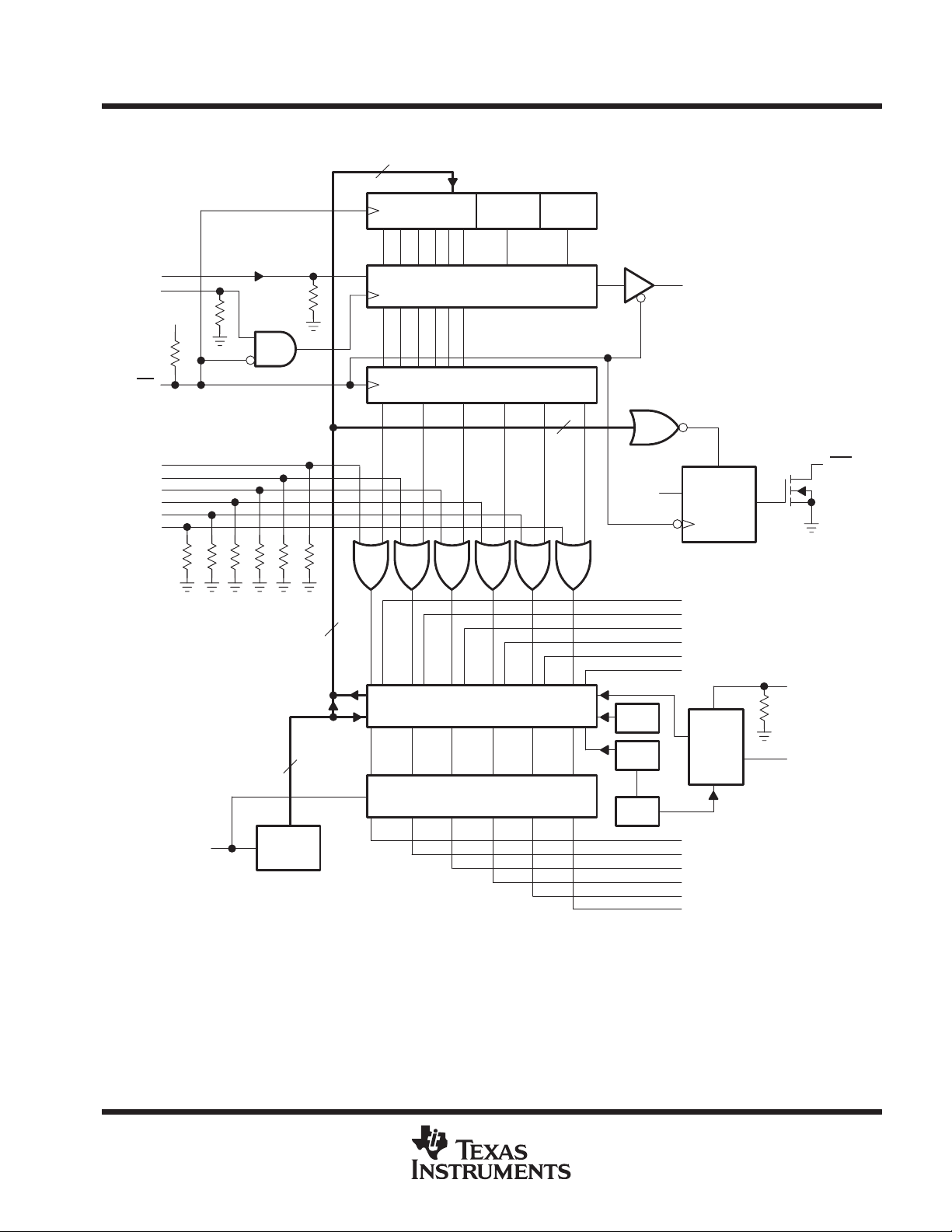
schematic diagram
TPIC46L01, TPIC46L02, TPIC46L03
6-CHANNEL SERIAL AND PARALLEL LOW-SIDE PRE-FET DRIVER
SLIS055A – NOVEMBER 1996 - REVISED SEPTEMBER 1997
8
Fault Logic UVLO†OVLO
SDI
SCLK
CS
IN 0
IN 1
IN 2
IN 3
IN 4
IN 5
Serial Register
V
CC
Parallel Register
8
GND
8
6
STB and Open-Load Fault
Protection
OSC
SDO
PREZ
D
DRAIN 0
DRAIN 1
DRAIN 2
DRAIN 3
DRAIN 4
DRAIN 5
S
FLT
Q
VCOMPEN
V
BAT
†
UVLO is not in TPIC46L03
2
OVLO
UVLO
BIAS
Gate
Drive Block
†
POST OFFICE BOX 655303 • DALLAS, TEXAS 75265
V
bg
B
A
GATE 0
GATE 1
GATE 2
GATE 3
GATE 4
GATE 5
VCOMP
3
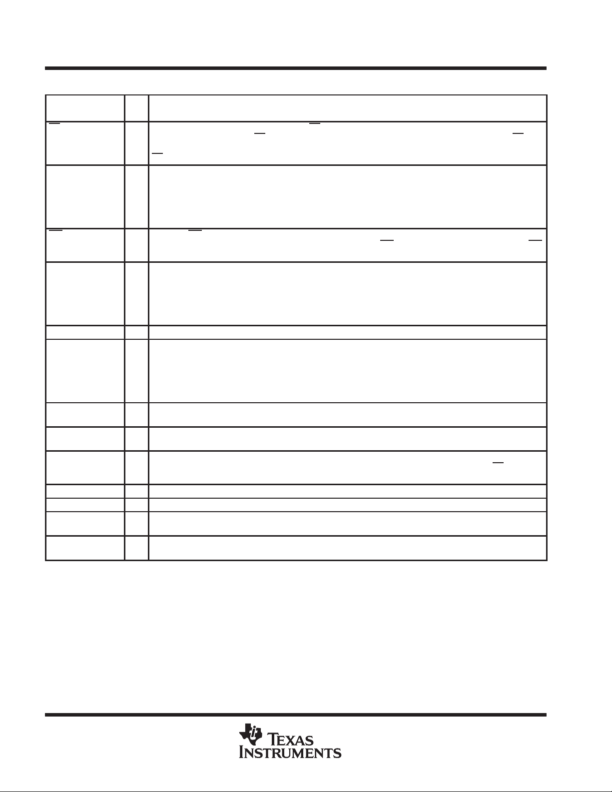
TPIC46L01, TPIC46L02, TPIC46L03
I/O
DESCRIPTION
6-CHANNEL SERIAL AND PARALLEL LOW-SIDE PRE-FET DRIVER
SLIS055A – NOVEMBER 1996 - REVISED SEPTEMBER 1997
Terminal Functions
TERMINAL
NAME NO.
CS 10 I Chip select. A high to low transition on the CS enables SDO, latches fault data into the serial interface, and
DRAIN0
DRAIN1
DRAIN2
DRAIN3
DRAIN4
DRAIN5
FLT 1 O Fault flag. FLT is an open-drain output that provides a real-time fault flag for shorted-load/open-load/over-battery
GATE0
GATE1
GATE2
GATE3
GATE4
GATE5
GND 15 I Ground and substrate
IN0
IN1
IN2
IN3
IN4
IN5
SCLK 13 I Serial clock. SCLK clocks the shift register. Serial data is clocked into SDI and serial fault data is clocked out of
SDI 12 I Serial data input. Output control data is clocked into the serial register through SDI. A 1 on SDI commands a
SDO 11 O Serial data output. SDO is a 3-state output that transfers fault data to the controling device. It also passes serial
V
BAT
V
CC
VCOMPEN 2 I Fault reference voltage select. VCOMPEN selects the internally generated fault reference voltage (0) or an
VCOMP 3 I Fault reference voltage. VCOMP provides an external fault reference voltage for the shorted- and open-load fault
26
24
23
20
19
17
27
25
22
21
18
16
4
5
6
7
8
9
28 I Battery supply voltage input
14 I Logic supply voltage
refreshes the fault flag. When CS
data is latched into the serial output register and transferred using SDO and SCLK. On a low to high transition of
CS
, serial data is latched in to the output control register.
I FET drain inputs. DRAIN0 through DRAIN5 are used for both open-load and short-circuit fault detection at the drain
of the external FETs. They are also used for inductive transient protection.
voltage/under-battery voltage faults. The device can be ORed with FL T
requires an external pullup resistor.
O Gate drive output. GATE0 through GA TE5 outputs are derived from the V
voltages on these nodes from exceeding the VGS rating on most FETs.
I Parallel gate driver inputs. IN0 through IN5 are real-time controls for the gate predrive circuitry. They are CMOS
compatible with hysteresis.
SDO on the falling edge of the serial clock.
particular gate output on and a 0 turns it off.
input data to the next stage for cascaded operation. SDO is taken to a high-impedance state when CS
state.
external fault reference (1) to be used in the shorted- and open-load fault detection circuitry .
detection circuitry.
is high, the fault registers can change fault status. On the falling edge of CS, fault
on other devices for interrupt handling. FLT
supply. Internal clamps prevent the
BAT
is in a high
4
POST OFFICE BOX 655303 • DALLAS, TEXAS 75265
TPIC46L01, TPIC46L02, TPIC46L03
6-CHANNEL SERIAL AND PARALLEL LOW-SIDE PRE-FET DRIVER
SLIS055A – NOVEMBER 1996 - REVISED SEPTEMBER 1997
absolute maximum ratings over operating free-air temperature range (unless otherwise noted)
Supply voltage range, V
Battery supply voltage range, V
Input voltage range,V
Output voltage range, V
Drain-to-source input voltage, V
Output voltage, V
–0.3 V to 15 V. . . . . . . . . . . . . . . . . . . . . . . . . . . . . . . . . . . . . . . . . . . . . . . . . . . . . . . . . . . . . . .
O
Operating case temperature range, T
Thermal resistance, junction to ambient, R
Operating virtual junction temperature range, T
Storage temperature range, T
†
Stresses beyond those listed under “absolute maximum ratings” may cause permanent damage to the device. These are stress ratings only, and
functional operation of the device at these or any other conditions beyond those indicated under “recommended operating conditions” is not
implied. Exposure to absolute-maximum-rated conditions for extended periods may affect device reliability.
NOTE 1: All voltage values are with respect to GND.
(see Note 1) –0.3 V to 7 V. . . . . . . . . . . . . . . . . . . . . . . . . . . . . . . . . . . . . . . . . . . . . .
CC
(at any input) –0.3 V to 7 V. . . . . . . . . . . . . . . . . . . . . . . . . . . . . . . . . . . . . . . . . . . . . . . . . .
I
(SDO and FLT) –0.3 V to 7 V. . . . . . . . . . . . . . . . . . . . . . . . . . . . . . . . . . . . . . . . . . . .
O
–0.3 V to 60 V. . . . . . . . . . . . . . . . . . . . . . . . . . . . . . . . . . . . . . . . . . . . . . . . .
BA T
–0.3 V to 60 V. . . . . . . . . . . . . . . . . . . . . . . . . . . . . . . . . . . . . . . . . . . . . . . . . .
DS
–40°C to + 125°C. . . . . . . . . . . . . . . . . . . . . . . . . . . . . . . . . . . . . . . . . . .
C
–40°C to + 150°C. . . . . . . . . . . . . . . . . . . . . . . . . . . . . . . . . . . . . . . . . . . . . . . .
stg
112°C/W. . . . . . . . . . . . . . . . . . . . . . . . . . . . . . . . . . . . . . . . . . . . .
θJA
150°C. . . . . . . . . . . . . . . . . . . . . . . . . . . . . . . . . . . . . . . . . . . . .
J
recommended operating conditions
MIN NOM MAX UNIT
Logic supply voltage, V
Battery supply voltage, V
High-level input voltage, V
Low-level input voltage, V
Setup time, SDI high before SCLK rising edge, tsu (see Figure 5) 10 ns
Hold time, SDI high after SCLK rising edge, th (see Figure 5) 10 ns
Case temperature, T
CC
BAT
IH
IL
C
4.5 5.0 5.5 V
8 24 V
0.85 V
CC
0 0.15 V
–40 125 °C
V
CC
CC
V
V
†
POST OFFICE BOX 655303 • DALLAS, TEXAS 75265
5
TPIC46L01, TPIC46L02, TPIC46L03
Gate disabled
See Figure 16
Gate disabled
See Figure 17
VGGate drive voltage
6-CHANNEL SERIAL AND PARALLEL LOW-SIDE PRE-FET DRIVER
SLIS055A – NOVEMBER 1996 - REVISED SEPTEMBER 1997
electrical characteristics over recommended operating free-air temperature range (unless
otherwise noted)
PARAMETER TEST CONDITIONS MIN TYP MAX UNIT
I
BAT
I
CC
V
(turnon)
V
(ovsd)
V
hys(ov)
V
(uvsd)
V
hys(uv)
I
O(H)
I
O(L)
V
(stb)
V
hys(stb)
V
D(open)
V
hys(open)
I
I(open)
I
I(PU)
I
I(PD)
V
I(hys)
V
O(SH)
V
O(SL)
I
OZ(SD)
V
O(CFLT)
V
I(COMP)
V
C
V
C
Supply current, V
Supply current, V
Turn-on voltage, logic operational, V
Over-battery-voltage shutdown
Over-battery-voltage reset hysteresis
Under-battery-voltage shutdown,
(TPIC46L01, L02 only)
Under-battery-voltage reset hysteresis,
(TPIC46L01, L02 only)
Maximum current output for drive terminals,
pullup
Maximum current output for drive terminals,
pulldown
Short-to-battery/shorted-load/open-load
detection voltage
Short-to-battery hysteresis 40 100 150 mV
Open-load off-state detection drain voltage
threshold
Open-load hysteresis 40 100 150 mV
Open-load off-state detection current 30 60 80 µA
Input pullup current (CS) VCC = 5 V, VIN = 0 10 µA
Input pulldown current VCC = 5 V, VIN = 5 V 10 µA
Input voltage hysteresis VCC = 5 V 0.6 0.85 1.1 V
High-level serial output voltage IO = 1 mA 0.8 V
Low-level serial output voltage IO = 1 mA 0.1 0.4 V
3-state current serial-data output VCC = 0 to 5.5 V -10 1 10 µA
Fault-interrupt output voltage IO = 1 mA 0.1 0.5 V
Fault-external reference voltage VCOMPEN = H 1 3 V
Output clamp voltage, (TPIC46L01, L02 only) dc < 1%, tw = 100 µs 47 55 63 V
Output clamp voltage, (TPIC46L03 only) dc < 1%, tw = 100 µs 47 60 V
BAT
CC
CC
All outputs off, V
All outputs off, V
V
= 5.5 V,
BAT
Check output functionality
,
,
8 V < V
5.5 V < V
V
OUT
V
OUT
VCOMPEN = L 1.1 1.25 1.4 V
VCOMPEN = L 1.1 1.25 1.4 V
< 24, IO = 100 µA 7 13.5 V
BAT
< 8 V, IO = 100 µA 5 7 V
BAT
= GND 0.5 1.2 2.5 mA
= 7 V 0.5 1.2 2.5 mA
= 12 V 300 500 700 µA
BAT
= 5.5 V 1 2.6 4.2 mA
BAT
2.6 3.5 4.4 V
32 34 36 V
0.5 1 1.5 V
4.1 4.8 5.4 V
100 200 300 mV
CC
V
6
POST OFFICE BOX 655303 • DALLAS, TEXAS 75265

TPIC46L01, TPIC46L02, TPIC46L03
6-CHANNEL SERIAL AND PARALLEL LOW-SIDE PRE-FET DRIVER
SLIS055A – NOVEMBER 1996 - REVISED SEPTEMBER 1997
switching characteristics, V
PARAMETER TEST CONDITIONS MIN TYP MAX UNIT
t
(STBFM)
t
(STBDG)
t
PLH
t
PHL
t
r1
t
f1
f
(SCLK)
t
rf(SB)
t
w
t
d1
t
pd1
t
pd2
t
pd3
t
r2
t
f2
t
r3
t
f3
Mask time, short-to-battery/shorted-load/openload fault
Deglitch time, short-to-battery/shorted-load See Figure 14 8 µs
Propagation turn-on delay time, CS or IN0-IN5
to GATE0-GATE5
Propagation turn-off delay time, CS or IN0-IN5
to GATE0-GATE5
Rise time, GATE0–GATE5 C
Fall time, GATE0–GATE5 C
Serial clock frequency 10 MHz
Refresh time, short-to-battery TPIC46L02 only, See Figure 14 10 ms
Short-to-battery refresh pulse width TPIC46L02 only, See Figure 14 68 µs
Setup time, CS↓ to ↑SCLK See Figure 5 10 ns
Propagation delay time, CS↓ to SDI valid
Propagation delay time, SCLK↓ to SDI valid See Figure 6 20 ns
Propagation delay time, CS↑ to SDO 3-state
Rise time, SDO 3-state to SDO valid
Fall time, SDO 3-state to SDO valid
Rise time, FLT
Fall time, FLT
CC
= 5 V, V
= 12 V, T
BAT
See Figures 14 and 15 60 µs
C
(gate)
C
(gate)
(gate)
(gate)
RL = 10 kΩ,
See Figure 6
RL = 10 kΩ,
See Figure 7
RL = 10 kΩ to GND,
CL = 200 pF,
RL = 10 kΩ to VCC,
CL = 200 pF,
RL = 10 kΩ,
See Figure 10
RL = 10 kΩ,
See Figure 11
= 25°C
C
= 400 pF, See Figure 1 4 µs
= 400 pF, See Figure 2 3.5 µs
= 400 pF, See Figure 3 3.5 µs
= 400 pF, See Figure 4 3 µs
CL = 200 pF,
CL = 50 pF,
Over-battery fault,
See Figure 8
No faults,
See Figure 9
CL = 50 pF,
CL = 50 pF,
40 ns
2 µs
30 ns
20 ns
1.2 µs
15 ns
or IN0–IN5
CS
GATE0–GATE5
GATE0–GATE5
50%
Figure 1
Figure 3
10%
90%
90%
t
PLH
t
IN0–IN5
CS
GATE0–GATE5
50%
50%
t
PHL
10%
Figure 2
t
r1
GATE0–GATE5
90%
10%
f1
Figure 4
POST OFFICE BOX 655303 • DALLAS, TEXAS 75265
7

TPIC46L01, TPIC46L02, TPIC46L03
6-CHANNEL SERIAL AND PARALLEL LOW-SIDE PRE-FET DRIVER
SLIS055A – NOVEMBER 1996 - REVISED SEPTEMBER 1997
SCLK
SCLK
t
d1
SDI
CS
SDO
CS
SDO
t
su
Figure 5
50%
Figure 7
3-STATE
t
pd3
3-STATE
t
f2
90%
10%
CS
t
h
SDI
t
pd1
3-STATE
t
pd2
Figure 6
SDO
3-STATE
90%
10%
t
r2
Figure 8
t
r3
FLT
90%
10%
Figure 9
FLT
90%
10%
Figure 11
Figure 10
t
f3
8
POST OFFICE BOX 655303 • DALLAS, TEXAS 75265

TPIC46L01, TPIC46L02, TPIC46L03
6-CHANNEL SERIAL AND PARALLEL LOW-SIDE PRE-FET DRIVER
SLIS055A – NOVEMBER 1996 - REVISED SEPTEMBER 1997
PRINCIPLES OF OPERATION
serial data operation
The TPIC46L01, TPIC46L02, and TPIC46L03 offer serial input interfaces to the microcontroller to transfer
control data to the predriver and output fault data back to the controller. The serial input interface consists of:
• SCLK – Serial clock
• CS – Chip select
• SDI – Serial data input
• SDO – Serial data output
Serial data is shifted into the least significant bit (LSB) of the SDI shift register on the rising edge of the first SCLK
after CS
significant bit (MSB) of the shift register. Less than eight clock cycles result in fault data being latched into the
output control buffer . The first two bits are unused and the last six bits are the output control data. A low-to-high
transition on CS
turns the corresponding parallel output off and a 1 turns the output on (see Figure 12).
has transitioned from 1 to 0. Eight clock cycles are required to shift the first bit from the LSB to the most
latches the contents of the serial shift register into the output control register. A 0 input to SDI
12345678
SCLK
CS
SDI
New Data
Output Control
Register Data
Don’t Care
GATE5 OFF
GATE4 ON
GATE3 ON
GATE2 OFF
GATE1 OFF
GATE0 ON
Present Output Data New Data
Figure 12
POST OFFICE BOX 655303 • DALLAS, TEXAS 75265
9

TPIC46L01, TPIC46L02, TPIC46L03
6-CHANNEL SERIAL AND PARALLEL LOW-SIDE PRE-FET DRIVER
SLIS055A – NOVEMBER 1996 - REVISED SEPTEMBER 1997
PRINCIPLES OF OPERATION
serial data operation (continued)
Data is shifted out of SDO on the falling edge of SCLK. The MSB of fault data is available when CS is transitioned
low. The remaining 7 bits of fault data are shifted out on the following seven clock cycles. Fault data is latched
into the serial register when CS
CS
to be captured by the device. The CS input must be transitioned to a high state after the last bit of serial data
has been clocked into the device. CS
serial data into the output control register, and clears and re-enables the serial fault registers (see Figure 13).
When a shorted-load condition occurs with the TPIC46L01 or TPIC46L03, the controller must disable and
re-enable the channel to clear the fault register and fault flag. The TPIC46L02 automatically retries the output
and FLT
SCLK
clears after the fault condition has been corrected.
12345678
CS
is transitioned low. Fault data must be present on the high-to-low transition of
puts SDO in a high-impedance state, inhibits SDI, latches the 6 bits of
SDO 3-State UV FLT5 FLT4 FLT3 FLT2 FLT1 FLT0 N/A
O V
bit8
bit7 bit6 bit5 bit4 bit3 bit2 bit1
OV Over-Battery-Voltage Fault Bit
UV Under-Battery-Voltage Fault Bit
FLT5 Shorted- or Open-Load Fault on Channel 5
FLT4 Shorted- or Open-Load Fault on Channel 4
FLT3 Shorted- or Open-Load Fault on Channel 3
FLT2 Shorted- or Open-Load Fault on Channel 2
FLT1 Shorted- or Open-Load Fault on Channel 1
FLT0 Shorted- or Open-Load Fault on Channel 0
N/A Unknown Data
Figure 13
parallel input data operation
In addition to the serial input interface, the TPIC46L01 and TPIC46L02 also provides a parallel input interface
to the microcontroller. The output turns on if either the parallel or the serial interface commands it to turn on.
The parallel data pins are real-time control inputs for the output drivers. SCLK and CS
parallel input data to the output buffer . Fault data must be read over the serial data bus as described in the serial
data operation section of this data sheet. The parallel input must be transitioned low and then high to clear and
re-enable a gate output that has been disabled due to a shorted-load fault condition.
are not required to transfer
10
POST OFFICE BOX 655303 • DALLAS, TEXAS 75265

TPIC46L01, TPIC46L02, TPIC46L03
6-CHANNEL SERIAL AND PARALLEL LOW-SIDE PRE-FET DRIVER
SLIS055A – NOVEMBER 1996 - REVISED SEPTEMBER 1997
PRINCIPLES OF OPERATION
chipset performance under fault conditions
The TPIC46L01, TPIC46L02, TPIC46L03, and power FET array’s are designed for normal operation over a
battery-voltage range of 8 V to 24 V with load fault detection from 4.8 V to 34 V . The TPIC46L01, TPIC46L02,
and TPIC46L03 offer on-board fault detection to handle a variety of faults that may occur within a system. The
circuits primary function is to prevent damage to the load and the power FETs in the event that a fault occurs.
Unused DRAIN0–DRAIN5 inputs must be connected to V
of open-load fault conditions. This circuitry detects the fault, shuts off the output to the FET , and reports the fault
to the microcontroller. The primary faults under consideration are:
1. Shorted-load
2. Open-load
3. Over-battery voltage shutdown
4. Under-battery voltage shutdown
NOTE:
TPIC46L01 and TPIC46L02, an undervoltage fault may be detected when V
On the
applied to the device. The controller should initialize the fault register after power up to clear any
false fault reports.
through a pullup resistor to prevent false reporting
BA T
CC
and V
BAT
are
shorted–load fault condition
The TPIC46L01 and TPIC46L02 monitor the drain voltage of each channel to detect shorted-load conditions.
The on-board deglitch timer starts running when the gate output to the power FET transitions from the off state
to the on state. The timer provides a 60-µs deglitch time, t
(STBFM)
the power FET has been turned on. The deglitch time is only enabled for the first 60 µs after the FET has been
turned on. After the deglitch delay time, the drain voltage is checked to verify that it is less than the fault reference
voltage. When it is greater than the reference voltage for at least the short-to-battery deglitch time, t
FLT
flags the microcontroller that a fault condition exists and the gate output is automatically shut off
(TPIC46L01 and TPIC46L03) until the error condition has been corrected.
An overheating condition on the FET occurs when the controller continually tries to re-enable the output under
shorted-load fault conditions. When a shorted-load fault is detected while using the TPIC46L02, the gate output
is transitioned into a low-duty-cycle PWM signal to protect the FET from overheating. The PWM rate is defined
as t
and the pulse with is defined as tw. It remains in this low-duty-cycle pulse state until the fault has been
(SB)
corrected or until the controller disables the gate output.
The microcontroller can read the serial port on the predriver to isolate which channel reported the fault condition.
Fault bits 0–5 distinguish faults for each of the output channels. When a shorted-load condition occurs with the
TPIC46L01, the controller must disable and re-enable the channel to clear the fault register and fault flag. The
TPIC46L02 automatically retries the output and the fault clears after the fault condition has been corrected.
Figure 14 illustrates operation after a gate output has been turned on. The gate to the power FET is turned on
and the deglitch timer starts running. Under normal operation T1 turns on and the drain operates below the
reference point set at U1. The output of U1 is low and a fault condition is not flagged.
, to allow the drain voltage to stabilize after
(STBDG)
, then
POST OFFICE BOX 655303 • DALLAS, TEXAS 75265
11

TPIC46L01, TPIC46L02, TPIC46L03
6-CHANNEL SERIAL AND PARALLEL LOW-SIDE PRE-FET DRIVER
SLIS055A – NOVEMBER 1996 - REVISED SEPTEMBER 1997
PRINCIPLES OF OPERATION
External TPIC46L01/L02
V
BAT
Load
U1
+
_
Input From
TPIC46L01/L02
T1
N-Channel
1.25 V
Deglitch
FLT
NORMAL
Input
GATE0–
GATE5
Glitches
DRAIN0–
DRAIN5
FLT
SHORTED-LOAD TPIC46L02
Input
GATE0–
GATE5
DRAIN0–
DRAIN5
FLT
t
(STBFM)
Glitches
SHORTED-LOAD TPIC46L01 AND TPIC46L03
Input
GATE0–
GATE5
Glitches
DRAIN0–
DRAIN5
FLT
t
(STBDG)
t
(STBFM)
t
(SB)
t
w
GATE0–
GATE5
12
t
(STBDG)
t
(STBFM)
Figure 14
POST OFFICE BOX 655303 • DALLAS, TEXAS 75265

TPIC46L01, TPIC46L02, TPIC46L03
6-CHANNEL SERIAL AND PARALLEL LOW-SIDE PRE-FET DRIVER
SLIS055A – NOVEMBER 1996 - REVISED SEPTEMBER 1997
PRINCIPLES OF OPERATION
open load
The TPIC46L01, TPIC46L02, and TPIC46L03 monitor the drain of each power FET for open-circuit conditions
that may exist. The 60-µA current source is provided to monitor open-load fault conditions. Open-load faults are
detected when the power FET is turned off. When load impedance is open or substantially high, then the 60-µA
current source has adequate drive to pull the drain of T1 below the fault reference threshold on the detection
circuit. Unused DRAIN0–DRAIN5 inputs must be connected to V
reporting of open-load fault conditions. The on-board deglitch timer starts running when the TPIC46L01,
TPIC46L02, and TPIC46L03 gate output to the power FET transitions to the off state. The timer provides a 60-µs
deglitch time, t
(STBFM)
, to allow the drain voltage to stabilize after the power FET has been turned off. The
deglitch time is only enabled for the first 60 µs after the FET has been turned off. After the deglitch delay time,
the drain is checked to verify that it is greater than the fault reference voltage. When it is less than the reference
voltage, a fault is flagged to the microcontroller through FLT
microcontroller can then read the serial port on the TPIC46L01, TPIC46L02, and TPIC46L03 to isolate which
channel reported the fault condition. Fault bits 0–5 distinguish faults for each of the output channels. Figure 15
illustrates the operation of the open-load detection circuit. This feature provides useful information to the
microcontroller to isolate system failures and warn the operator that a problem exists. Examples of such
applications would be warning that a light bulb filament may be open, solenoid coils may be open, etc.
through a pullup resistor to prevent false
BA T
that an open-load fault condition exists. The
NORMAL
Input
GATE0–
GATE5
DRAIN0–
DRAIN5
FLT
TPIC46L01/L02/L03
Input From
Glitches
t
(STBFM)
V
BAT
T1
NORMAL
External TPIC46L01/L02/L03
Load
60 µA
N-Channel
1.25 V
Deglitch
OPEN-LOAD
Input
GATE0–
GATE5
DRAIN0–
DRAIN5
FLT
U1
+
_
t
(STBFM)
FLT
Figure 15
POST OFFICE BOX 655303 • DALLAS, TEXAS 75265
13

TPIC46L01, TPIC46L02, TPIC46L03
6-CHANNEL SERIAL AND PARALLEL LOW-SIDE PRE-FET DRIVER
SLIS055A – NOVEMBER 1996 - REVISED SEPTEMBER 1997
PRINCIPLES OF OPERATION
over-battery-voltage shutdown
The TPIC46L01, TPIC46L02, and TPIC46L03 monitor the battery voltage to prevent the power FET s from being
turned on in the event that the battery voltage is too high. This condition may occur due to voltage transients
resulting from a loose battery connection. The TPIC46L01/L02/L03 turns the power FETs off when the battery
voltage is above 34 volts, to prevent possible damage to the load and the FETs. The gate output goes back to
normal operation after the overvoltage condition has been corrected. An over-battery-voltage fault is flagged
to the controller through the fault flag. Bit 8 of the serial-data fault word is set whenever an over-battery voltage
condition is present. When an overvoltage condition occurs the device reports the battery fault, but disables fault
reporting for open and shorted-load conditions. Fault reporting for open and shorted-load conditions re-enables
after the battery-fault condition has been corrected. When the fault condition is removed before the CS
transitions low, then the fault condition is not captured in the serial fault register. FLT
transition of CS
provided no other faults are present in the device. Figure 16 illustrates the operation of the
over-battery voltage-detection circuit.
V
BAT
resets on the high-to-low
signal
V
BAT
GATE0–GATE5
34 V
34 V
+
_
Figure 16
Output Disable
33 V12 V
14
POST OFFICE BOX 655303 • DALLAS, TEXAS 75265

TPIC46L01, TPIC46L02, TPIC46L03
6-CHANNEL SERIAL AND PARALLEL LOW-SIDE PRE-FET DRIVER
SLIS055A – NOVEMBER 1996 - REVISED SEPTEMBER 1997
PRINCIPLES OF OPERATION
under-battery-voltage shutdown (TPIC46L01, and TPIC46L02 only)
The TPIC46L01 and TPIC46L02 monitor the battery voltage to prevent the power FETs from being turned on
in the event that the battery voltage is too low. When the battery voltage is below 4.8 volts, then GA TE0–GA TE5
outputs may not provide sufficient gate voltage to the power FET s to minimize the on-resistance that could result
in a thermal stress on the FET . The output resumes normal operation after the under-voltage condition has been
corrected. An under-battery voltage fault flags the controller through the fault flag. Bit 7 of the serial-data fault
word is set whenever an under-battery voltage condition is present. When an under-battery voltage condition
occurs the device reports the battery fault, but disables fault reporting for open- and shorted-load conditions.
When the fault condition is removed before CS
serial fault register. FLT
resets on the high-to-low transition of CS provided no other faults are present in the
device. Figure 17 illustrates the operation of the under-battery voltage-detection circuit.
signal transitions low, the fault condition is not captured in the
V
BAT
U1
_
4.8 V
+
Output Disable
V
BAT
GATE0–GATE5
12 V
5 V
4.8 V
Figure 17
POST OFFICE BOX 655303 • DALLAS, TEXAS 75265
15

TPIC46L01, TPIC46L02, TPIC46L03
6-CHANNEL SERIAL AND PARALLEL LOW-SIDE PRE-FET DRIVER
SLIS055A – NOVEMBER 1996 - REVISED SEPTEMBER 1997
PRINCIPLES OF OPERATION
Inductive voltage transients
A typical application for the predriver/power FET circuit is to switch inductive loads. When an inductive load is
switched off, a large voltage spike can occur . These spikes can exceed the maximum V
FET and damage the device when proper protection is not in place. The FET can be protected from these
transients through a variety of methods using external components. The TPIC46L01 and TPIC46L02 offer that
protection in the form of a zener diode stack connected between the drain input and GA TE output (see Figure
18). Zener diode (Z1) turns the FET on to dissipate the transient energy . GA TE diode (Z2) is provided to prevent
the gate voltage from exceeding 13 volts during normal operation and transient protection.
TPIC46L01/02 External
rating for the external
DS
Z1
Z2
55 V
13 V
DRAIN
GATE
Figure 18
LOAD
Power FET
V
BAT
16
POST OFFICE BOX 655303 • DALLAS, TEXAS 75265

TPIC46L01, TPIC46L02, TPIC46L03
6-CHANNEL SERIAL AND PARALLEL LOW-SIDE PRE-FET DRIVER
SLIS055A – NOVEMBER 1996 - REVISED SEPTEMBER 1997
PRINCIPLES OF OPERATION
external fault reference input
The TPIC46L01, TPIC46L02, and TPIC46L03 compare each channel drain voltage to a fault reference to detect
shorted-load and open-load conditions. The user has the option of using the internally generated 1.25-V fault
reference or providing an external reference voltage through VCOMP . The internal reference voltage is selected
by connecting VCOMPEN to GND and VCOMP is selected by connecting VCOMPEN
Proper layout techniques should be used in the grounding network for the VCOMP
TPIC46L01/L02/L03. The ground for the predriver and the VCOMP
network should be connected to a Kelvin
ground if available; otherwise, a single point connection should be maintained to the power ground of the FET
array. Improper grounding techniques may result in inaccuracies in detecting faults.
External TPIC46L01/L02
to V
(see Figure 19).
CC
circuit and the
DRAIN5
DRAIN0
VCOMP
VCOMPEN
1.25 V
VCOMP
1.25 V
VCOMPEN
0
1
A
M
U
X
Figure 19
+
_
+
_
Deglitch
U1
FLT
POST OFFICE BOX 655303 • DALLAS, TEXAS 75265
17

TPIC46L01, TPIC46L02, TPIC46L03
6-CHANNEL SERIAL AND PARALLEL LOW-SIDE PRE-FET DRIVER
SLIS055A – NOVEMBER 1996 - REVISED SEPTEMBER 1997
MECHANICAL DATA
DB (R-PDSO-G**) PLASTIC SMALL-OUTLINE PACKAGE
28 PIN SHOWN
0,65
28
1
2,00 MAX
0,38
0,22
15
14
A
0,05 MIN
0,15
M
5,60
5,00
Seating Plane
8,20
7,40
0,10
0,15 NOM
Gage Plane
0°–8°
0,25
1,03
0,63
PINS **
DIM
A MAX
A MIN
NOTES: A. All linear dimensions are in millimeters.
B. This drawing is subject to change without notice.
C. Body dimensions do not include mold flash or protrusion not to exceed 0,15.
D. Falls within JEDEC MO-150
8
3,30
2,70
14
6,50
6,50
5,905,90
2016
7,50
6,90
24
8,50
28
10,50
9,907,90
30
10,50
9,90
38
12,90
12,30
4040065 /C 10/95
18
POST OFFICE BOX 655303 • DALLAS, TEXAS 75265

IMPORTANT NOTICE
T exas Instruments and its subsidiaries (TI) reserve the right to make changes to their products or to discontinue
any product or service without notice, and advise customers to obtain the latest version of relevant information
to verify, before placing orders, that information being relied on is current and complete. All products are sold
subject to the terms and conditions of sale supplied at the time of order acknowledgement, including those
pertaining to warranty, patent infringement, and limitation of liability.
TI warrants performance of its semiconductor products to the specifications applicable at the time of sale in
accordance with TI’s standard warranty. Testing and other quality control techniques are utilized to the extent
TI deems necessary to support this warranty . Specific testing of all parameters of each device is not necessarily
performed, except those mandated by government requirements.
CERT AIN APPLICATIONS USING SEMICONDUCTOR PRODUCTS MAY INVOLVE POTENTIAL RISKS OF
DEATH, PERSONAL INJURY, OR SEVERE PROPERTY OR ENVIRONMENTAL DAMAGE (“CRITICAL
APPLICATIONS”). TI SEMICONDUCTOR PRODUCTS ARE NOT DESIGNED, AUTHORIZED, OR
WARRANTED TO BE SUITABLE FOR USE IN LIFE-SUPPORT DEVICES OR SYSTEMS OR OTHER
CRITICAL APPLICA TIONS. INCLUSION OF TI PRODUCTS IN SUCH APPLICATIONS IS UNDERST OOD TO
BE FULLY AT THE CUSTOMER’S RISK.
In order to minimize risks associated with the customer’s applications, adequate design and operating
safeguards must be provided by the customer to minimize inherent or procedural hazards.
TI assumes no liability for applications assistance or customer product design. TI does not warrant or represent
that any license, either express or implied, is granted under any patent right, copyright, mask work right, or other
intellectual property right of TI covering or relating to any combination, machine, or process in which such
semiconductor products or services might be or are used. TI’s publication of information regarding any third
party’s products or services does not constitute TI’s approval, warranty or endorsement thereof.
Copyright 1998, Texas Instruments Incorporated
 Loading...