Texas Instruments TPIC44H01DAR, TPIC44H01DA Datasheet
TPIC44H01
4-CHANNEL SERIAL AND PARALLEL HIGH-SIDE PRE-FET DRIVER
SLIS088 – SEPTEMBER 1998
1
POST OFFICE BOX 655303 • DALLAS, TEXAS 75265
D
Serial or Parallel Control of Gate Outputs
D
Sleep State for Low Quiescent Current
D
Independent On-State Source
Short-to-Ground (Shorted-Load)
Detection/Protection
D
Independent On-State Over-Current
Detection/Protection With Dynamic Fault
Threshold
D
Independent Off-State Open-Load
Detection
D
Supply Over-Voltage Lockout Protection
D
Asynchronous Open-Drain Fault Interrupt
Terminal to Flag Fault Conditions. Output
Can be OR’ed With Multiple Devices
D
Encoded Fault Status Reporting Through
Serial Output Terminal (2-Bits Per Channel)
D
Programmable On-State Fault Deglitch
Timers
D
High Impedance CMOS Compatible Inputs
With Hysteresis
D
Fault Mode Selection: Outputs Latched Off
or Switched at Low Duty Cycle
D
Device Can be Cascaded With Serial
Interface
description
The TPIC44H01 is a four channel high-side pre-FET driver which provides serial or parallel input interface to
control four external NMOS power FETs. It is designed for use in low frequency switching applications for
resistive or inductive loads, including solenoids and incandescent bulbs.
Each channel has over-current, short-to-ground, and open-load detection that is flagged through the FLT
pin
and distinguished through the serial interface. Over-current thresholds are set through the V
(PK_x)
and
V
(COMP1-4)
pins. Short-to-ground and open-load thresholds are set internally to approximately 2.5 V. The
AR_ENBL pin is used to define the operation of the device during a fault condition, allowing the outputs to either
latch off or to enter a low duty cycle, auto-retry mode. An over-voltage lockout circuit on V
(PWR)
protects the
device and the external FETs. A low current sleep state mode is provided to allow the TPIC44H01 to be used
in applications where V
(PWR)
is connected directly to the battery. An internal charge pump allows the use of
N-channel FET s for high-side drive applications, while current-limit gate drive provides slope control for reduced
RFI.
By having the unique ability to develop a dynamic over-current threshold, the TPIC44H01 can be used to drive
incandescent bulbs with long inrush currents without falsely flagging a fault. Likewise, the user can select an
internally set over-current threshold of ~1.25 V by pulling the respective V
(COMP1-4)
pin to VCC.
Copyright 1998, Texas Instruments Incorporated
PRODUCTION DATA information is current as of publication date.
Products conform to specifications per the terms of Texas Instruments
standard warranty. Production processing does not necessarily include
testing of all parameters.
Please be aware that an important notice concerning availability, standard warranty, and use in critical applications of
Texas Instruments semiconductor products and disclaimers thereto appears at the end of this data sheet.
TI is a trademark of Texas Instruments Incorporated.
1
2
3
4
5
6
7
8
9
10
11
12
13
14
15
16
32
31
30
29
28
27
26
25
24
23
22
21
20
19
18
17
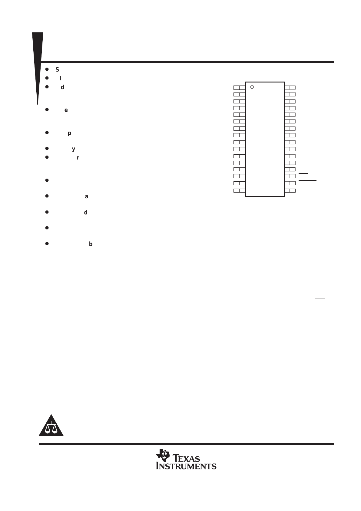
CS
SD0
SDI
SCLK
AR_ENBL
GND
IN1
IN2
IN3
IN4
V
CC
V
(PK_A)
V
(PK_B)
V
(COMP1)
V
(COMP2)
V
(COMP3)
PGND
V
(PWR)
CP1
CP2
V
(CP)
GATE1
SRC1
GATE2
SRC2
GATE3
SRC3
GATE4
SRC4
FL T
RESET
V
(COMP4)
DA PACKAGE
(TOP VIEW)

TPIC44H01
4-CHANNEL SERIAL AND PARALLEL HIGH-SIDE PRE-FET DRIVER
SLIS088 – SEPTEMBER 1998
2
POST OFFICE BOX 655303 • DALLAS, TEXAS 75265
description (continued)
The 8-bit serial peripheral interface (SPI) allows the user to command any of the four outputs on or off, to
program one of eight possible open-load, over-current, and short-load fault deglitch timer settings, and to
engage the sleep state. Data is clocked into the SDI pin on the rising edge of SCLK and clocked out of the SDO
pin on the SCLK falling edge. The serial input bits are logic OR’ed with the IN1-IN4 parallel inputs pins. The serial
interface is also used to read normal-load, open-load, over-current, and short-to-ground conditions for each
channel. Over-voltage lockout can be detected when the FL T
pin is low and no bits are set in the SDO register.
Multiple TPIC44H01 devices may be cascaded together using the serial interface to further reduce I/O lines from
the host controller.
TPIC44H01
4-CHANNEL SERIAL AND PARALLEL HIGH-SIDE PRE-FET DRIVER
SLIS088 – SEPTEMBER 1998
3
POST OFFICE BOX 655303 • DALLAS, TEXAS 75265
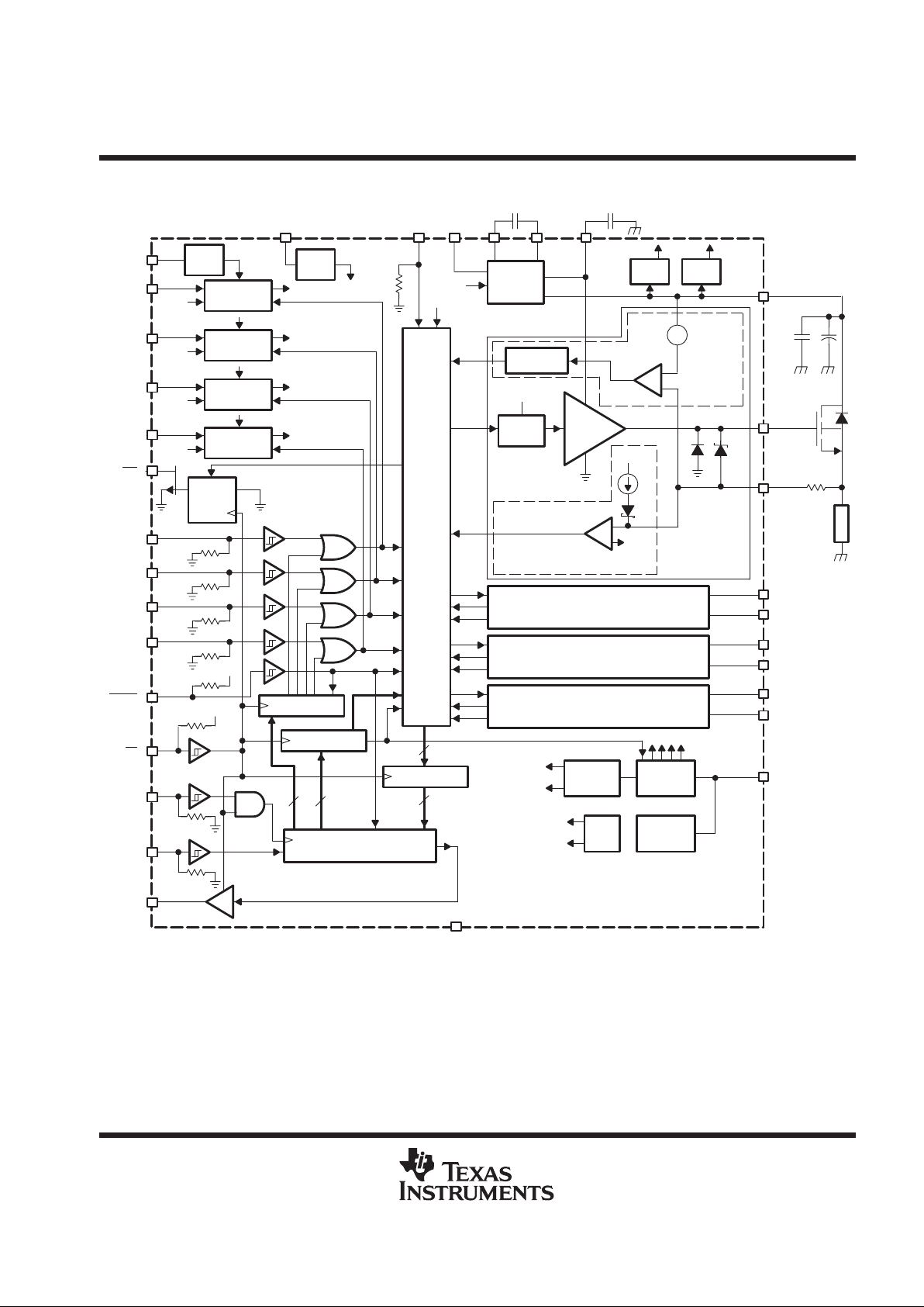
schematic/block diagram
V
V
peak
Buffer
V
(PK_A)
OVDS V
thres
Generation
OVDS V
thres
Generation
V
(COMP1)
V
bg
V
(COMP2)
V
bg
OVDS V
thres1
OVDS V
thres2
V
peakA
V
peakA
OVDS V
thres
Generation
V
(COMP3)
V
bg
OVDS V
thres3
V
peakB
OVDS V
thres
Generation
V
(COMP4)
V
bg
OVDS V
thres4
V
peakB
QD
CLK
PS
FLT
IN1
IN2
IN3
IN4
V
CC
RESET
V
peak
Buffer
V
peakB
V
(PK_B)
Parallel Reg
Control Reg
V
CC
CS
Sleep
t
DG
Gate Drive and
Fault Protection Logic
AR_ENBL
OVLO
Charge
Pump
0.01 µF
CP
0.1 µF
CS
PGND
CP1
CP2
V
(CP)
OVLO
OSC
5-V
V
reg
OVLO 5-V Int
+
–
OVDS
V
thres
+
–
OVDS t
DG
Comp
Over-V
DS
Detect
HS Gate
Drive
Gate
Control
+
–
7-V Int
+
–
Comp
I
5-V Int
2 V
bg
On-State ShortLoad Detect
Off-State OpenLoad Detect
Channel 1
Output
Channel 2 Output
Channel 3 Output
Channel 4 Output
GATE2
SRC2
GATE3
SRC3
GATE4
SRC4
Global
Ibias
Band Gap
I
bias
Sleep
8
Fault Logic
Serial Shift Register
4 4
SCLK
SDI
SDO
Tri-State Buffer
2 V
bg
V
bg
UVLO/
POR
OSC
Charge Pump
Digital Deglitch
V
CC
0.1 µF1 µF
+
LOAD
100 Ω
SRC1
GATE1
V
(PWR)
8
t
AR
GND
TPIC44H01
4-CHANNEL SERIAL AND PARALLEL HIGH-SIDE PRE-FET DRIVER
SLIS088 – SEPTEMBER 1998
4
POST OFFICE BOX 655303 • DALLAS, TEXAS 75265
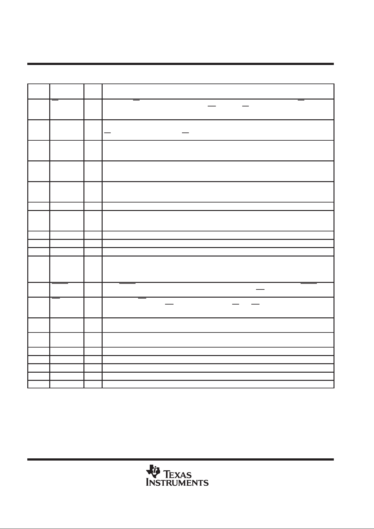
Terminal Functions
PIN PIN
NO. NAME
I/O
DESCRIPTION
1 CS I Chip Select. CS is an active low, logic level input with internal pullup. A logic level low on CS enables the
serial interface and refreshes the fault interrupt (FLT
). A high on CS enables the serial register to serve as
the fault data register.
2 SDO O Serial Data Output. SDO is a logic level, tri-state output that transfers fault data to the host controller. Serial
input data passes to the next stage for cascade operation. SDO is forced into a high impendance state when
CS
terminal is in a high state. When CS is in a low state, data is clocked out on each falling edge of SCLK.
3 SDI I Serial Data Input. SDI is a logic level input with hysteresis and internal pulldown. Gate drive output control
data is clocked into the serial register using SDI. A high SDI bit programs a particular gate output on, and a
low turns it off, as long as the parallel input is off (OR function).
4 SCLK I Serial Clock. SCLK is a logic level input with hysteresis and internal pulldown. SCLK clocks data at the SDI
terminal into the input serial shift register on each rising edge, and shifts out fault data (and serial input data
for cascaded operation) to the SDO pin on each falling edge.
5 AR_ENBL I Auto-Retry Enable. AR_ENBL is a logic level input with hysteresis and internal pulldown. When
AR_ENBL=0, an over-current/short-to-ground fault latches the channel off. When AR_ENBL = 1, an
over-current/short-to-ground fault engages a low duty cycle operation.
6 GND I Analog ground and substrate connection
7–10 IN1-4 I Parallel Inputs. IN1-4 are logic level inputs with hysteresis and internal pulldown. IN1–4 provide real-time
control of gate pre-drive circuitry. A high on IN1-4 will turn on corresponding gate drive outputs (GATE1-4).
Gate output status is a logic OR function of the parallel inputs and the serial input bits.
11 V
CC
I 5-V logic supply voltage
12 V
(PK_A)
I Dynamic over-current fault threshold peak voltage that is shared by channels 1 and 2
13 V
(PK_B)
I Dynamic over-current fault threshold peak voltage that is shared by channels 3 and 4
14–17 V
(COMP1-4)
I Fault Reference Voltage. V
(COMP1–4)
are used to provide an external fault reference voltage for the
over-current fault detection circuitry. It is also used to generate a dynamic threshold when used in conjunction
with V
(PK_x)
. To guarantee V
(COMP)
stability, a minimum of 100 pF capacitance should be placed from
V
(COMP)
to ground.
18 RESET I Reset. RESET is an active low, logic level input with hysteresis and internal pullup. A low on RESET clears
all registers and fault bits. All gate outputs are turned off and a latched FLT
interrupt is cleared.
19 FLT O Fault Interrupt. FLT is an active low , logic level, open-drain output providing real-time latched fault interrupts
for fault detection. A latched FLT
is cleared only by a low on CS. The FLT terminal can be OR’ed with other
devices for fault interrupt handling. An external pullup is required.
20, 22,
24, 26
SRC1-4 I FET Source Inputs. These inputs are used for both open-load and over-current fault detection at the source
of the external FETs.
21, 23,
25, 27
GATE1-4 O Gate Drive Outputs. Output voltage is derived from V
(CP)
supply voltage. Internal clamps prevent the voltage
on these nodes, with respect to SRC1-4, from exceeding the VGS rating of most FETs.
28 V
(CP)
O Charge pump voltage storage capacitor and supply pin to high-side gate drives
29 CP2 O Charge pump capacitor terminal
30 CP1 O Charge pump capacitor terminal
31 V
(PWR)
I Power supply voltage input
32 PGND I Power ground for charge pump
TPIC44H01
4-CHANNEL SERIAL AND PARALLEL HIGH-SIDE PRE-FET DRIVER
SLIS088 – SEPTEMBER 1998
5
POST OFFICE BOX 655303 • DALLAS, TEXAS 75265
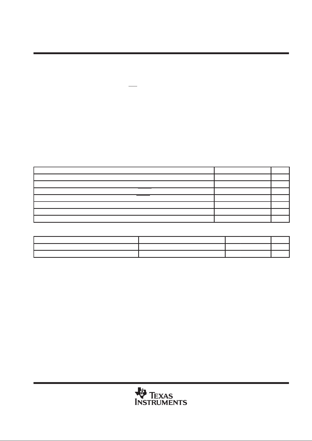
absolute maximum ratings over operating free-air temperature (unless otherwise noted)
†
Logic supply voltage range, V
CC
(see Note 1) –0.3 V to 7 V. . . . . . . . . . . . . . . . . . . . . . . . . . . . . . . . . . . . . . . . .
Power supply voltage range, V
(PWR)
(see Note 1) –0.3 V to 40 V. . . . . . . . . . . . . . . . . . . . . . . . . . . . . . . . . . . .
Input voltage range, V
I
(see Note 1) –0.3 V to 7 V. . . . . . . . . . . . . . . . . . . . . . . . . . . . . . . . . . . . . . . . . . . . . . . . . .
Output voltage range, V
O
(SDO and FLT, see Note 1) –0.3 V to 7 V. . . . . . . . . . . . . . . . . . . . . . . . . . . . . . . . . .
Source input voltage, V
I(SRCx)
(see Note 1) –3 V to 40 V. . . . . . . . . . . . . . . . . . . . . . . . . . . . . . . . . . . . . . . . . . . .
Output voltage, V
O(GA TEx)
(see Note 1) –0.3 V to 45 V. . . . . . . . . . . . . . . . . . . . . . . . . . . . . . . . . . . . . . . . . . . . .
Logic input current, I
I
±25 µA. . . . . . . . . . . . . . . . . . . . . . . . . . . . . . . . . . . . . . . . . . . . . . . . . . . . . . . . . . . . . . . . . . . .
Operating case temperature range, T
C
–40°C to 125°C. . . . . . . . . . . . . . . . . . . . . . . . . . . . . . . . . . . . . . . . . . . . .
Operating virtual junction temperature range, T
J
–40°C to 150°C. . . . . . . . . . . . . . . . . . . . . . . . . . . . . . . . . . . . .
Storage temperature range, T
stg
–65°C to 150°C. . . . . . . . . . . . . . . . . . . . . . . . . . . . . . . . . . . . . . . . . . . . . . . . . . .
†
Stresses beyond those listed under “absolute maximum ratings” may cause permanent damage to the device. These are stress ratings only, and
functional operation of the device at these or any other conditions beyond those indicated under “recommended operating conditions” is not
implied. Exposure to absolute-maximum-rated conditions for extended periods may affect device reliability.
NOTE 1: All voltage values are with respect to GND.
recommended operating conditions
MIN TYP MAX UNIT
Logic supply voltage, V
CC
4.5 5 5.5 V
Power supply voltage, V
(PWR)
8 24 V
High level logic input voltage, VIH (all logic inputs except RESET) 0.7×V
CC
V
CC
V
Low level logic input voltage, VIL (all logic inputs except RESET) 0 0.3×V
CC
V
Setup time, SDI high before SCLK rising edge, tsu (see Figure 5) 10 ns
Hold time, SDI high after SCLK rising edge, th (see Figure 5) 10 ns
Operating case temperature, T
C
–40 125 °C
thermal resistance
PARAMETER TEST CONDITIONS MIN TYP MAX UNIT
R
θJA
Junction-to-ambient thermal resistance Using JEDEC, low K, board configuration 86.04 °C/W
R
θJC
Junction-to-case thermal resistance 7.32 °C/W

TPIC44H01
4-CHANNEL SERIAL AND PARALLEL HIGH-SIDE PRE-FET DRIVER
SLIS088 – SEPTEMBER 1998
6
POST OFFICE BOX 655303 • DALLAS, TEXAS 75265
electrical characteristics over recommended operating case temperature and supply voltage
range (unless otherwise noted)
†
PARAMETER TEST CONDITIONS MIN TYP MAX UNIT
I
(PWR)
V
(PWR)
supply current All outputs off, V
(PWR)
= 12 V 2 4 6 mA
I
CCH
5-V supply current All outputs off, VCC = 5.5 V 3 4 5 mA
p
p
p
I
-
p
Slee state current
Slee state (all out uts off)
,
15 40
µ
A
I
(PWR-slee )
(I
PWR
)
V
CC
= 5.5 V,
V
(PWR)
= 12 V,
T
C
=
25°C
15
40
µA
p
p
p
I
p
Slee state current
Slee state (all out uts off)
,
30 40
µ
A
I
CCL(slee )
(I
CCL
)
V
CC
= 5.5 V,
V
(PWR)
= 12 V,
T
C
=
25°C
30
40
µA
V
IT(POR)
Power-on reset
threshold, V
CC
V
(PWR)
= 5.5 V, VCC increasing 3.4 3.9 4.4 V
V
hys(POR)
Power-on reset
threshold hysteresis,
V
CC
V
(PWR)
= 5.5 V, VCC decreasing 100 300 500 mV
V
> 24 V, CP = 0.01 µF, CS = 0.1 µF,
(PWR)
, µ , µ ,
I
(CP)
= –2 mA, See Figure 8
40
44
V
V
(PWR)
= 24 V, CP = 0.01 µF, CS = 0.1 µF,
38 40 42 V
p
p
I
(CP)
= –2 mA, See Figure
8
384042
V
V
(CP)
Charge um voltage
V
= 8 V, CP = 0.01 µF, CS = 0.1 µF,
(PWR)
, µ , µ ,
I
(CP)
= –2 mA, See Figure 8
11.5
13.5
V
V
(PWR)
= 5.5 V, CP = 0.01 µF,
CS = 0.1 µF, I
(CP)
= –2 mA, See Figure 8
6.8 7.5 V
V
(OVLO)
Over-supply voltage
lockout
Gate disabled, See Figure 10 27.5 30 32.5 V
V
hys(OV)
Over-supply voltage
reset hysteresis
See Figure 10 0.5 1 2 V
8 V < V
< 24 V, I
= –100 µA,
(PWR)
,
O
µ ,
All channels on, See Note 2
V
(PWR)
+
4
V
(PWR)
+
18
V
VGGate drive voltage
5.5 V < V
< 8 V, I
= –100 µA,
(PWR)
,
O
µ ,
All channels on, See Note 2
V
(PWR)
+1.
5
V
(PWR)
+3.
5
V
V
G(sleep)
External gate sleep
state voltage
IO = 100 µA, RESET = CS = 0 V 0 100 300 mV
V
GS(clamp)
Gate-to-source clamp
voltage
SRCx = 0 V, Output on 15 17 19.5 V
V
SG(clamp)
Source-to-gate clamp
voltage
Output off, II = 100 µA 6.5 8 9.5 V
Gate drive source
VG = 0 V, V
(PWR)
= 12 V –2.3 –3 –3.7
I
G(SRCx)
current
VG = 10 V, V
(PWR)
= 12 V
–1.4 –2 –2.6
mA
Gate drive sink
VG = 2 V, V
(PWR)
= 12 V 1 1.5 2
I
G(SNKx)
current
VG= V
(PWR)
= 12 V
2 2.6 3.2
mA
V
(open)
SRCx pin off-state
open-load detection
threshold
All outputs off, See Figure 1 1 1.9 2.4 2.6 V
V
hys(open)
Off-state open-load
hysteresis
All outputs off –50 –150 –300 mV
†
Device will function with degraded performance for a power supply voltage between 5.5 V and 8 V .
NOTE 2: For characterization purposes only, not implemented in production testing.

TPIC44H01
4-CHANNEL SERIAL AND PARALLEL HIGH-SIDE PRE-FET DRIVER
SLIS088 – SEPTEMBER 1998
7
POST OFFICE BOX 655303 • DALLAS, TEXAS 75265
electrical characteristics over recommended operating case temperature and supply voltage
range (unless otherwise noted)
†
(continued)
PARAMETER TEST CONDITIONS MIN TYP MAX UNIT
I
(open)
Off-state open-load
detection current
All outputs off –20 –50 –70 µA
V
(COMPx)
> VCC – 250 mV 1 1.25 1.5 V
V
(OVDS)
Drain-to-source
-
0.1 V < V
< 2.5 V, 0.95 × V
–15 1.05 × V
+15
()
over voltage
(COMPx)
,
See Figures 12 and 13
(COMPx)
mV
(COMPx)
mV
V
V
(STG)
On-state
short-to-ground
detection voltage
See Figure 17 1.9 2.35 2.6 V
V
hys(STG)
On-state
short-to-ground
hysteresis
–50 –150 –300 mV
I
(pullup)
Logic input pullup
current
(CS
, RESET)
VCC = 5 V, VIN = 0 V –5 –20 –50 µA
I
(pulldown)
Logic input pulldown
current (IN1–4, SCLK,
SDI, AR_ENBL)
VCC = 5 V, VIN = 5 V 5 20 50 µA
V
hys
Logic input voltage
hysteresis (IN1–4,
SCLK, SDI, AR_ENBL,
CS
)
VCC = 5 V 0.5 0.8 1.2 V
V
OH
High level serial output
voltage
IO = –1 mA 0.8×V
CC
4.96 V
V
OL
Low level serial output
voltage
IO = 1 mA 0 100 400 mV
I
OZ
Serial data output
tri-state current
V
(SDO)
= 5.5 V to 0 V,
VCC = 5.5 V
–35 1 35 µA
V
OL(FLT)
FLT low level output
voltage
IO = 220 µA 0 30 350 mV
I
lkg(FLT)
FLT leakage current R
(pullup)
= 25 K, VCC = 5.5 V 0 1 20 µA
V
IH(RESET)
RESET high level logic
input voltage
1.9 2.2 V
CC
V
V
IL(RESET)
RESET low level logic
input voltage
0 1.2 1.4 V
V
hys(RESET)
Logic input voltage
hysteresis (RESET
)
VCC = 5 V 0.6 1 1.4 V
†
Device will function with degraded performance for a power supply voltage between 5.5 V and 8 V .
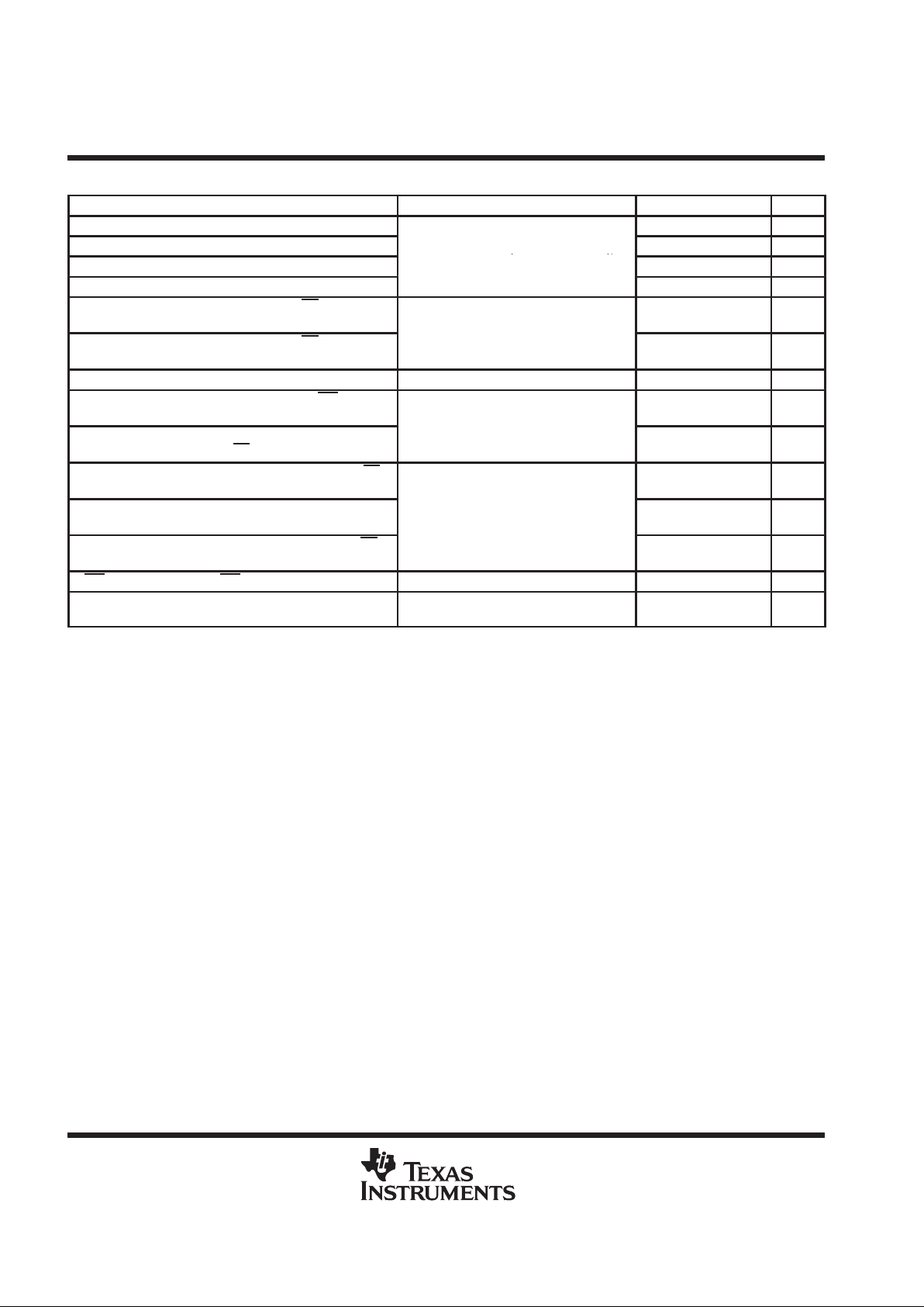
TPIC44H01
4-CHANNEL SERIAL AND PARALLEL HIGH-SIDE PRE-FET DRIVER
SLIS088 – SEPTEMBER 1998
8
POST OFFICE BOX 655303 • DALLAS, TEXAS 75265
switching characteristics, VCC = 5 V, V
(PWR)
= 12 V, TC = 25°C
PARAMETER TEST CONDITIONS MIN TYP MAX UNIT
t
(STG)
Short-to-ground deglitch time 16 µs
t
(OC)
Over-current deglitch time
SDI bits DG1–3 = 0 (default after POR),
120 µs
t
(OL)
Open-load deglitch time
(),
See Figures 11, 12, and 17 and Table 4
120 µs
t
(retry)
Auto-retry time 15 ms
t
PLH
Propagation turn-on delay, CS or IN1–4 to
GATE1–4
p
5 µs
t
PHL
Propagation turn-off delay, CS or IN1–4 to
GATE1–4
C
G
=
400 pF
,
See Figures 1 and 2
5 µs
f
(SCLK)
Serial clock frequency t
(WH)
= t
(WL)
= 0.5/f
(SCLK)
, See Figure 5 1 5 MHz
t
su(lead)
Setup from the falling edge of CS to the
rising edge of SCLK
100 ns
t
su(lag)
Setup from the falling edge of SCLK to
rising edge of CS
See Figure 5
100 ns
t
pd(SDOEN)
Propagation delay from falling edge of CS
to SDO valid
50 ns
t
pd(valid)
Propagation delay from falling edge of
SCLK to SDO valid
RL = 10 kΩ, CL = 200 pF, See Figure 5
50 ns
t
pd(SDODIS)
Propagation delay from rising edge of CS
to SDO Hi-Z state
150 ns
t
f(FLT)
Fall time of FLT output RL = 10 kΩ, CL = 200 pF, See Figure 3 12 ns
t
(active)
POR-to-active status delay, sleep-to-active
status delay
See Figure 4 512 µs
TPIC44H01
4-CHANNEL SERIAL AND PARALLEL HIGH-SIDE PRE-FET DRIVER
SLIS088 – SEPTEMBER 1998
9
POST OFFICE BOX 655303 • DALLAS, TEXAS 75265
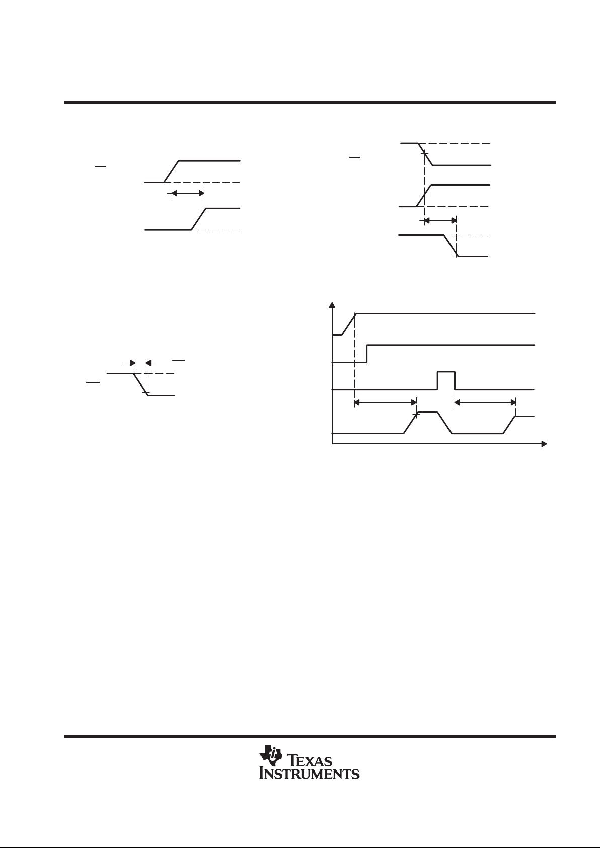
PARAMETER MEASUREMENT INFORMATION
Figure 1. Gate Control Turn-On
t
PLH
V
CC
V
(CP)
0 V
0 V
50%
V
(PWR)
CS
or IN1–4
GATE1–4
90%
Figure 2. Gate Control Turn-Off
50%
50%
V
CC
0 V
t
PHL
10%
V
(CP)
0 V
CS or IN1–4
GATE1–4
V
CC
0 V
Figure 3. Fault Interrupt Fall Time
V
CC
90%
10%
tf
(FLT)
0 V
FLT
Figure 4. Power-Up Waveforms
t
(active)
t
(active)
POR Threshold
V
CC
Input
Internal
Sleep Bit
GATEx
 Loading...