TPIC43T01, TPIC43T02
THREE-PHASE BRUSHLESS MOTOR RPM CONTROLLERS
SLIS098 – APRIL 2000
1
POST OFFICE BOX 655303 • DALLAS, TEXAS 75265
D
Precision Phase Lock Loop Motor – RPM
Control With Embedded DSP Filter
Algorithm for Loop Compensation
D
EEPROM Registers for User Adjustment of
PLL Loop Gain and DSP Filter Coefficients
(Pole/Zero)
D
Crystal Oscillator With EEPROM Adjustable
Divide-By for Versatile PLL Timebase
D
Standalone Operation With No Host
Processor Needed
D
RPM Lock Detection/Reporting
(±5% Window)
D
Synchronous Rectification,
Enabled (TPIC43T01)
Disabled (TPIC43T02)
D
Stalled Motor Timer/Shutdown
D
High-Side Current Limiting
D
High-Side Over-Current Shutdown
D
Differential Hall Effect Position Sensor
Inputs/Decode Provide Commutation
Control
D
Differential Variable Reluctance Speed
Sensor Inputs
D
Gate Drive for Six External N-Channel
Power FETs in Three Half-H Configuration
D
Charge Pump to Develop High-Side Gate
Drive V oltage
D
5 V Regulator – Designed for 10 mA
External Current
D
8 to 28 V Supply Voltage
D
Small Outline Surface-Mount Package
description
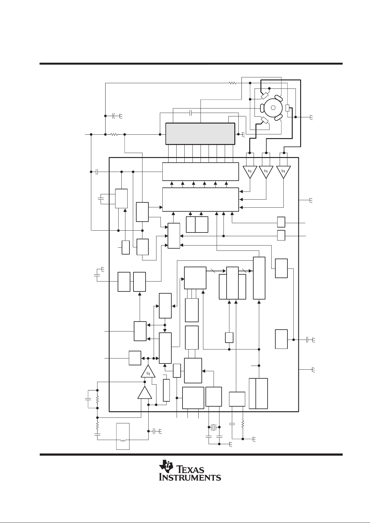
The TPIC43T01/02 is a monolithic motor control integrated circuit designed to provide RPM control to a 3-phase
brushless dc motor. The device provides two analog sensor input ports which include a speed sensor interface
and a Hall effect position interface. The speed feedback interface consists of an FG amplifier to receive an
external sinusoidal signal from a variable reluctance pickup and convert it to a digital speed signal for the control
circuit. When the motor speed is outside a ±5% window of the reference signal, an out-of-lock condition is
declared. The Hall ffect sensor input section receives low-level differential voltages from external naked Hall
elements and converts them to digital position reference signals for the control circuit for commutation control.
The core of the control circuit implements a digital signal processing algorithm consisting of a digital integrator
and filter with user adjustable parameters to optimize the closed loop performance of the control system. The
device contains an internal EEPROM to set integrator gain and digital filter coefficients. In addition, Texas
Instruments provides a PC based Windows compatible software package to input the motor and system
characteristics and convert them to control parameters for the TPIC43T01/02. The software generates a JEDEC
compatible file to program the device through a third party device programmer.
PRODUCTION DATA information is current as of publication date.
Products conform to specifications per the terms of Texas Instruments
standard warranty. Production processing does not necessarily include
testing of all parameters.
Please be aware that an important notice concerning availability, standard warranty, and use in critical applications of
Texas Instruments semiconductor products and disclaimers thereto appears at the end of this data sheet.
1
2
3
4
5
6
7
8
9
10
11
12
13
14
15
16
17
18
19
38
37
36
35
34
33
32
31
30
29
28
27
26
25
24
23
22
21
20
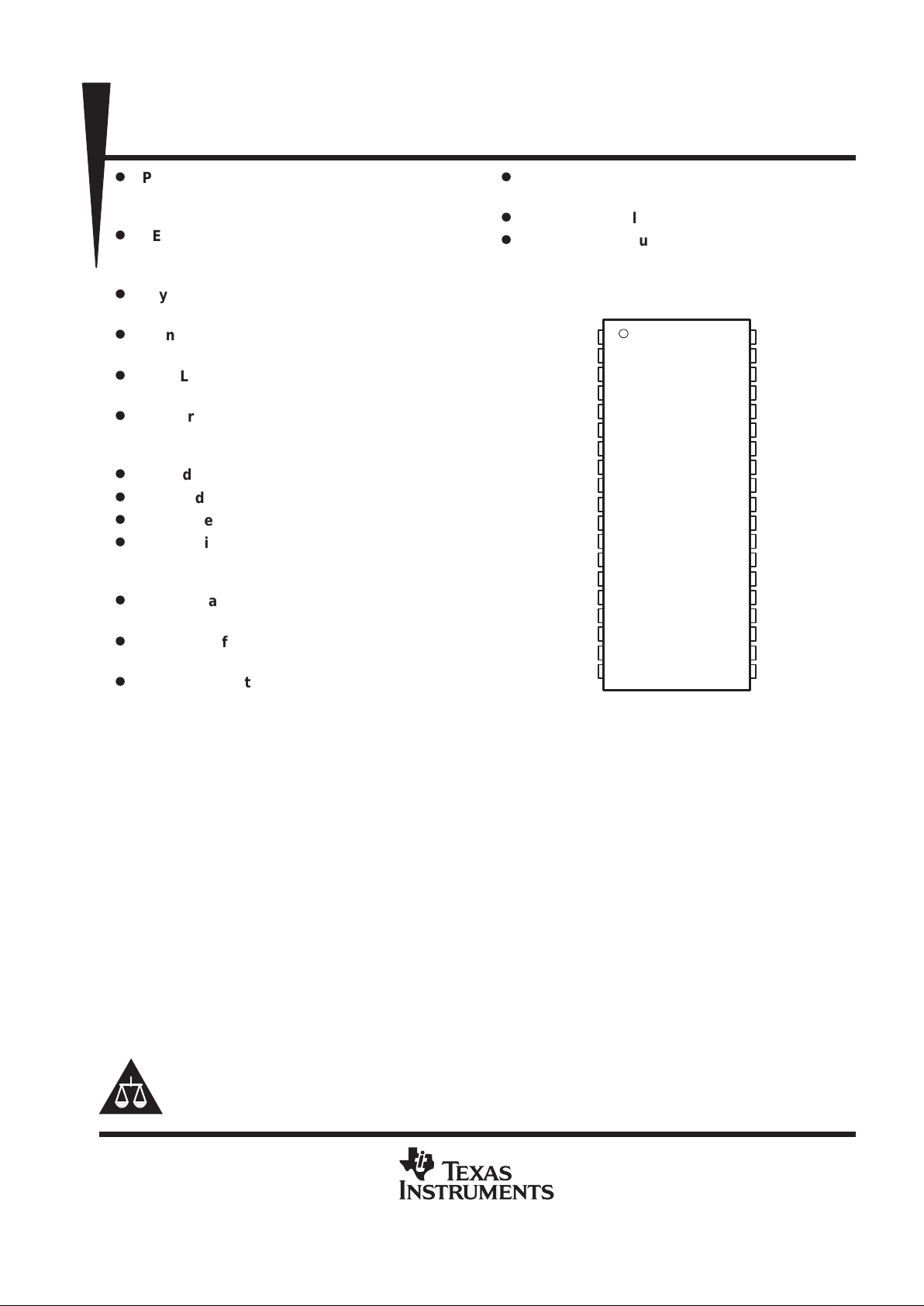
IN2+
IN2–
IN3+
IN3–
FGOUT
FGIN–
FGIN+
CLT
CT
RT
OSC2
OSC1
V
DD
FGSOUT
GND
LD
FSEL
S/S
F/R
IN1–
IN1+
TEST
V
PP
PHA
UGA
LGA
UGB
PHB
LGB
LGC
UGC
PHC
SENSE
CP2
CP1
V
CP
PGND
V
CC
DA PACKAGE
(TOP VIEW)
Copyright 2000, Texas Instruments Incorporated
Windows is a trademark of Microsoft Corporation.

TPIC43T01, TPIC43T02
THREE-PHASE BRUSHLESS MOTOR RPM CONTROLLERS
SLIS098 – APRIL 2000
2
POST OFFICE BOX 655303 • DALLAS, TEXAS 75265
description (continued)
The TPIC43T01/02 provides pre-drive outputs to control six external N-channel FET switches connected in a
3-half H-bridge configuration to drive a 3-phase dc motor. A companion TI Power+ Arrays device is available,
the TPIC1310 3-half H-bridge power array, to provide up to 2.5 A motor drive capability. The TPIC1310 is a
monolithic gate protected DMOS power array available in the TI 15-pin PowerFLEX power package. The
TPIC43T01/02 gate drive outputs are designed to also drive discrete N-channel power FETs.
The TPIC43T01/02 provides onboard supervisory and shutdown logic to protect the device and motor from fault
conditions. Oscillators, charge pump, and voltage regulators have been integrated into the TPIC43T01/02 to
minimize the number of external discrete components required to support the motor system.
Power+ Arrays and PowerFLEX are trademarks of Texas Instruments Incorporated.
TPIC43T01, TPIC43T02
THREE-PHASE BRUSHLESS MOTOR RPM CONTROLLERS
SLIS098 – APRIL 2000
POST OFFICE BOX 655303 DALLAS, TEXAS 75265
• 3
A2
+
–
+
FGS
OUT
Lock
Detect
FGS Bias
VIN
÷ 2
Speed
Discrimination
EEPROM
Program
and Test
Logic
FG
Frequency
Select
FG Divide
Register 1
F0
F1
FG Ref
OSC
F
S
OSC
Freq Adj REG
5.8 MHz
OSC
Gain Select
Register
A0
A1
Digital
Integrator
OSC_INT
–
Digital
Filter
10
k2:3–Bit REG
k1:6–Bit REG
8
8–Bit PWM
Generator
÷
FILTCLK
F
S
Watchdog
Timer
Lock
OSC
Lock
Counter
Shutdown
Logic
÷ 32
Charge
Pump
CP
UVLO
Current
Limit
181 kHz
CPUV
OCSD
Gate Drive
Control and
Commutation
Logic
Sync
Rect
VDDUV S/S
PWM
S/S
F/R
ILIM
Pre-FET
Drivers
–
+
–
+
F/RS/S
V
DD
UVLO
5 V
VReg
OSC_INT
FGOUT FGSOUT LD CLT
V
CC
CP1 CP2
V
CP
SENSE
UGA
PHA
LGA
UGB
PHB
LGB
UGC
PHC
LGC
IN1+
IN1–
IN2+
IN2–
IN3+
IN3–
PGNDF/RS/SV
DD
GND
FGIN–
FGIN+
FSEL
V
PP
TEST
OSC1
OSC2
CT
RT
Power
Array
IC
3-Phase
Motor
Analog Hall-Effect
Position Sensors
CM = 22 µF
Rsense
0.2
CP = 0.01 µF
V
m
CS = 0.1–0.5 µF
CLT = 0.1 µF
150 pF
330 k
1 k
1 µF
Speed
Pickup
FG
0.01 µF
Cosc = 30 pF
Cosc = 30 pF
CT = 0.02 µF
RT = 12.5 k
1 µF
typical application
0.1 µF
1.5 k
Coast
TPIC43T01, TPIC43T02
THREE-PHASE BRUSHLESS MOTOR RPM CONTROLLERS
SLIS098 – APRIL 2000
4
POST OFFICE BOX 655303 • DALLAS, TEXAS 75265
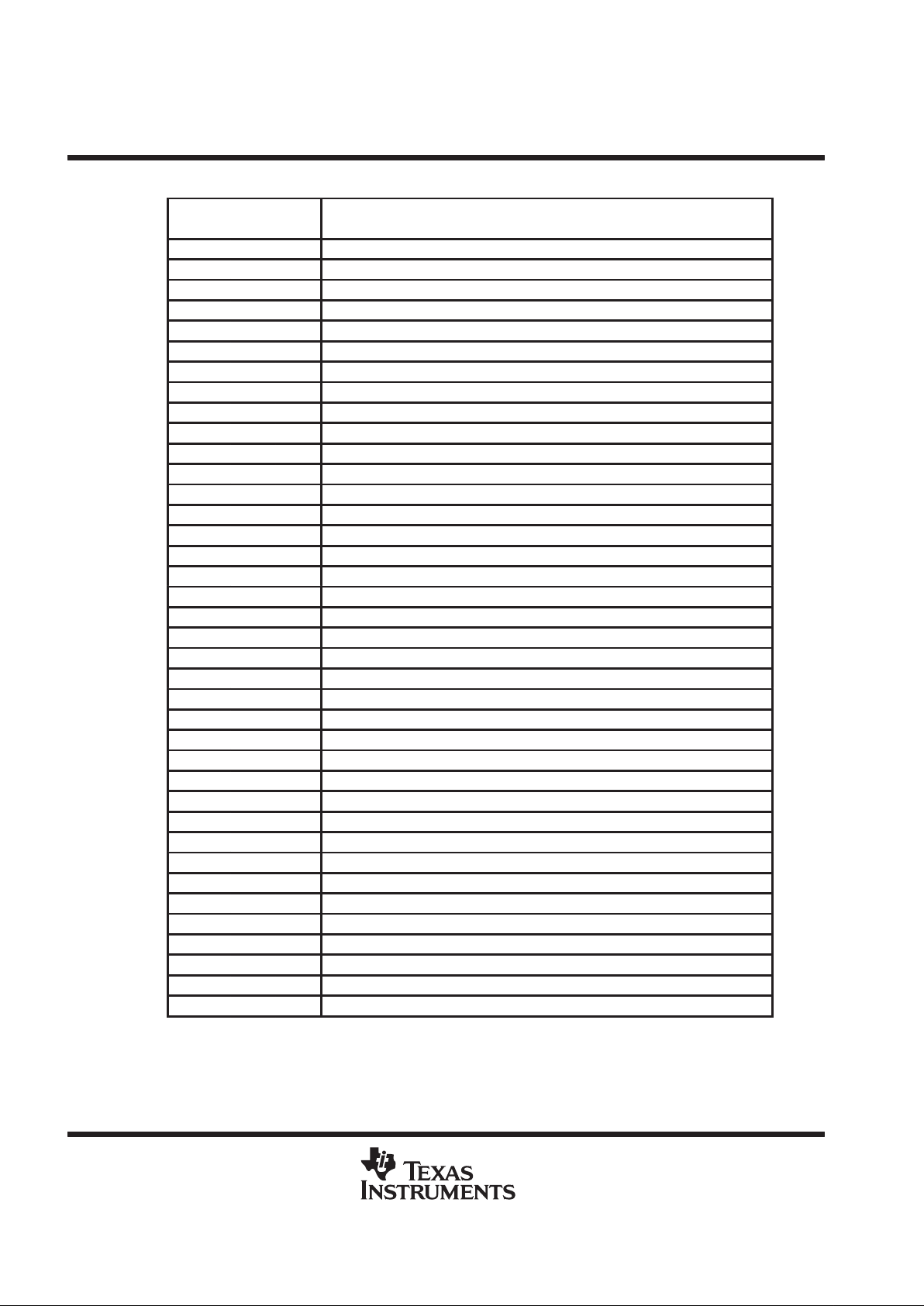
Terminal Functions
TERMINAL
NAME NO. I/O
DESCRIPTION
CLT 8 I Capacitor lock timer. CLT is a timing capacitor for the lock detect timer oscillator.
CP1 23 O Charge pump. CP1 is the switched capacitor output number 1.
CP2 24 O Charge pump. CP2 is the switched capacitor output number 2.
CT 9 I Timing capacitor. CT is the timing capacitor for the filter oscillator.
F/R 19 I Forward/Reverse. F/R is the forward/reverse direction data input.
FGIN– 6 I FGIN– is a inverting amplifier input.
FGIN+ 7 O FGIN+ is a noninverting amplifier input.
FGOUT 5 O FGOUT is a amplifier output.
FGSOUT 14 O FGSOUT is a buffered FGS comparator output.
FSEL 17 I Frequency select. FSEL is a frequency select input.
GND 15 Ground
IN1– 38 I Hall amplifier 1 inverting input
IN1+ 37 I Hall amplifier 1 noninverting input
IN2– 2 I Hall amplifier 2 inverting input
IN2+ 1 I Hall amplifier 2 noninverting input
IN3– 4 I Hall amplifier 3 inverting input
IN3+ 3 I Hall amplifier 3 non-inverting input
LD 16 O Lock Detect. LD is an active low, open-drain output.
LGA 32 I Lower gate drive A
LGB 29 I Lower gate drive B
LGC 28 I Lower gate drive C
OSC1 12 I Crystal oscillator input 1. OSC1 is an external OSC input.
OSC2 11 I Crystal oscillator input 2. OSC2 is an external OSC input.
PGND 21 PGND is the lower gate drive turnoff circuitry GND return.
PHA 34 I Phase A return
PHB 30 I Phase B return
PHC 26 I Phase C return
RT 10 O RT is the charge/discharge current setting resistor for filter and lock timer oscillators.
S/S 18 I Stop/Start. S/S = low to start.
SENSE 25 I Current limit sense. SENSE is the high-side current limit sense input.
TEST 36 I Test enable
UGA 33 I Upper gate drive A
UGB 31 I Upper gate drive B
UGC 27 I Upper gate drive C
V
CC
20 I Supply voltage
V
CP
22 O Charge-pump voltage source. VCP requires a storage capacitor.
V
DD
13 O 5 V Supply output
V
PP
35 I EEPROM programming voltage input
TPIC43T01, TPIC43T02
THREE-PHASE BRUSHLESS MOTOR RPM CONTROLLERS
SLIS098 – APRIL 2000
5
POST OFFICE BOX 655303 • DALLAS, TEXAS 75265
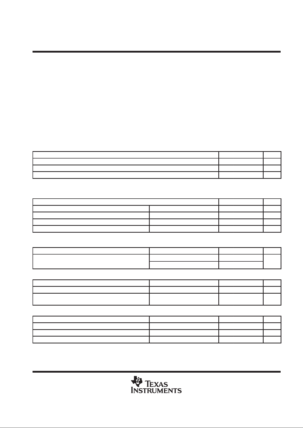
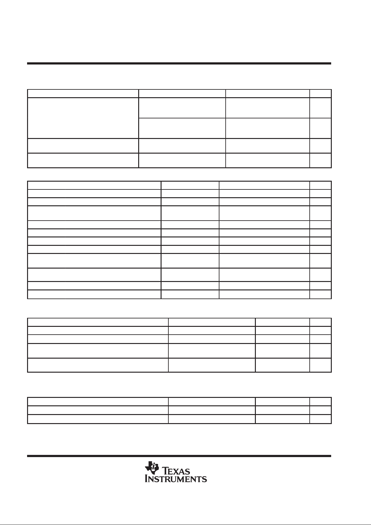
absolute maximum ratings over the recommended operating case temperature range (unless
otherwise noted)
†
Supply voltage range, VCC (see Note 1) 8 V to 30 V. . . . . . . . . . . . . . . . . . . . . . . . . . . . . . . . . . . . . . . . . . . . . . . .
Motor drive voltage, V
(motor)
30 V. . . . . . . . . . . . . . . . . . . . . . . . . . . . . . . . . . . . . . . . . . . . . . . . . . . . . . . . . . . . . . . .
Charge pump output voltage, V
CP(max),
(V
CP
– VCC) V
CC
+ 20 V. . . . . . . . . . . . . . . . . . . . . . . . . . . . . . . . . . . .
Operating virtual junction temperature range, TJ 0°C to 150°C. . . . . . . . . . . . . . . . . . . . . . . . . . . . . . . . . . . . . . .
Thermal resistance, junction to ambient, R
θJA
121°C/W. . . . . . . . . . . . . . . . . . . . . . . . . . . . . . . . . . . . . . . . . . . . .
Storage temperature range, T
stg
–65°C to 150°C. . . . . . . . . . . . . . . . . . . . . . . . . . . . . . . . . . . . . . . . . . . . . . . . . . .
Lead temperature 1,6 mm (1/16 inch) from case for 10 seconds 260°C. . . . . . . . . . . . . . . . . . . . . . . . . . . . . . .
†
Stresses beyond those listed under “absolute maximum ratings” may cause permanent damage to the device. These are stress ratings only, and
functional operation of the device at these or any other conditions beyond those indicated under “recommended operating conditions” is not
implied. Exposure to absolute-maximum-rated conditions for extended periods may affect device reliability.
NOTE 1: The device will function, but may not meet all electrical specifications over this voltage range.
recommended operating conditions
MIN TYP MAX UNIT
Supply voltage, V
CC
18 24 28 V
Extended supply voltage range, (see Note 1) 8 18 V
Operating case temperature, T
C
0 70 °C
NOTE 1: The device will function, but may not meet all electrical specifications over this voltage range.
EEPROM programming
MIN TYP MAX UNIT
VPP setup time, tsu(VPP) See Figure 20 2 µs
VPP pulse width duration, tw(VPP) See Figure 20 5 ms
VPP rise time, tr(VPP) See Figure 20 2 3 ms
VPP fall time, tf(VPP) See Figure 20 2 3 ms
electrical characteristics, TC = 25°C, V
CC
= 24V (unless otherwise noted)
PARAMETER TEST CONDITIONS MIN TYP MAX UNIT
S/S low, VCC = 28 V, I
(VCP)
= 2 mA
10 18
I
ccq
V
DD
quiescent current
S/S high, VCC = 28 V, I
(VCP)
= 0 mA
5 10
mA
VDD undervoltage lockout
PARAMETER TEST CONDITIONS MIN TYP MAX UNIT
V
DD(uvlo)
VDD under-voltage lockout threshold voltage 2.5 3.1 4 V
V
hys
VDD under-voltage lockout threshold voltage
hysteresis
1.1 V
5 V regulator
PARAMETER TEST CONDITIONS MIN TYP MAX UNIT
V
DD
Output voltage IO = –10 mA 4.75 5 5.25 V
V
(REGIN)
Line regulation VCC = 8 V to 28 V 0 50 mV
V
(REGOUT)
Load regulation IO = 0 to –10 mA 20 100 mV
TPIC43T01, TPIC43T02
THREE-PHASE BRUSHLESS MOTOR RPM CONTROLLERS
SLIS098 – APRIL 2000
6
POST OFFICE BOX 655303 • DALLAS, TEXAS 75265
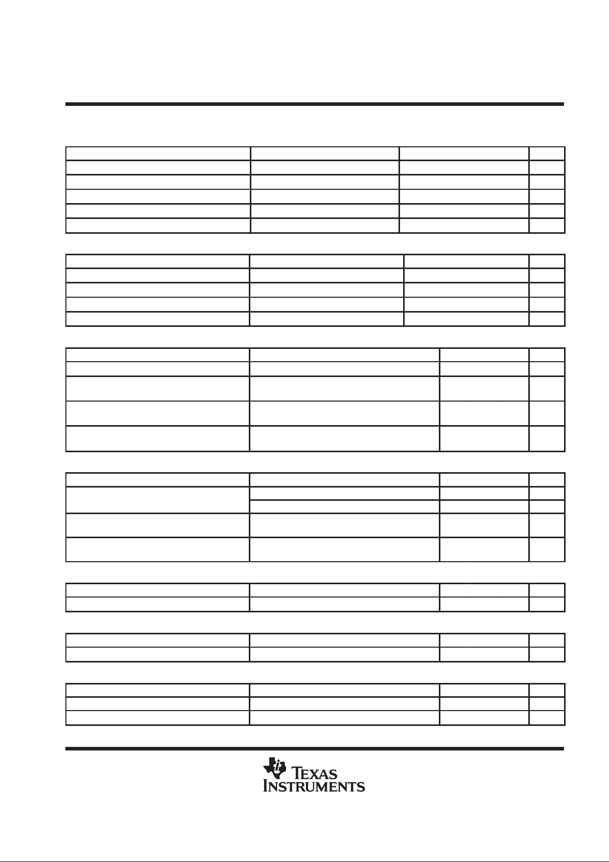
electrical characteristics, TC = 25°C, V
CC
= 24V (unless otherwise noted) (continued)
charge pump
PARAMETER TEST CONDITIONS MIN TYP MAX UNIT
p
IO = –1.5 mA, VCC = 18 V to 28 V,
CP = 0.01 µF, CS = 0.1 µF,
S/S = high
VCC + 14 VCC + 15 VCC + 17 V
V
O(CP)
Output voltage
IO = –1.5 mA, VCC = 8 V,
CP = 0.01 µF, CS = 0.1 µF,
S/S = high
VCC + 5.5 V
V
(CP–uvlo)
Under voltage lockout
IO = –1.5 mA, VCC = 8 V to 28 V,
S/S = high (VCP forced externally)
VCC + 5 VCC + 6 VCC + 7 V
V
hys(CP)
Under voltage lockout hysteresis
IO = –1.5 mA, VCC = 8 V to 28 V,
S/S = high (VCP forced externally)
0.6 V
FG signal conditioning
PARAMETER TEST CONDITIONS MIN TYP MAX UNIT
V
IO(FG)
Amplifier input offset voltage Measured at FGOUT 0.5 ±7 mV
I
IB(FG)
Amplifier input bias current Measured at FGIN– 0.02 ±1 µA
V
OH(FG)
Amplifier high level output voltage
I
(FG)
= –200 µA,
IDD = 0
VDD–500 mV VDD–350 mV V
V
OL(FG)
Amplifier low level output voltage I
(FG)
= 200 µA, IDD = 0 100 500 mV
A
V
Amplifier open-loop gain (see Note 2) 45 dB
V
(FGsens)
FG input sensitivity (see Note 2) 100 x Gain, at 2 kHz, 3 mV
V
(FGbias)
FG bias voltage IFG = 0 µA, IDD = 0 2.375 2.5 2.625 V
V
IT+(FGOUT)
FG comparator positive threshold
FGOUT with respect to
V
(FGIN+),
See Figure 8
215 250 285 mV
V
IO(FGOUT)
FG comparator offset voltage
FGOUT with respect to
V
(FGIN+)
, See Figure 8
0.8 ±7 mV
V
OL(FGSOUT)
FGSOUT open drain saturation voltage IO = 2 mA 0.4 0.7 V
I
lkg(FGSOUT)
FGSOUT leakage current VO = 5 V 0.08 10 µA
NOTE 2: Design target only. Not tested in production.
Hall sensor signal conditioning
PARAMETER TEST CONDITIONS MIN TYP MAX UNIT
I
IB(HL)
Input bias current (see Note 2) ±4 µA
V
ICR(HL)
Common-mode input voltage range (see Note 3) 1.5 3.5 V
V
IT+(HL)
Input positive threshold voltage
With respect to V
(CM)
, 1.5 kΩ in series
with both inputs, See Figure 9
4 8 12 mV
V
IT–(HL)
Input negative threshold voltage
With respect to VCM, 1.5 kΩ in series
with both inputs, See Figure 9
–4 –8 –12 mV
NOTES: 2. Design target only. Not tested in production.
3. Not measured, forced during testing.
FG reference crystal oscillator
PARAMETER TEST CONDITIONS MIN TYP MAX UNIT
V
IT+(OSC1)
OSC1 input upper threshold (see Note 3) 2.7 V
V
IT–(OSC1)
OSC1 input lower threshold (see Note 3) 1 V
NOTES: 3. Not measured, forced during testing.
TPIC43T01, TPIC43T02
THREE-PHASE BRUSHLESS MOTOR RPM CONTROLLERS
SLIS098 – APRIL 2000
7
POST OFFICE BOX 655303 • DALLAS, TEXAS 75265
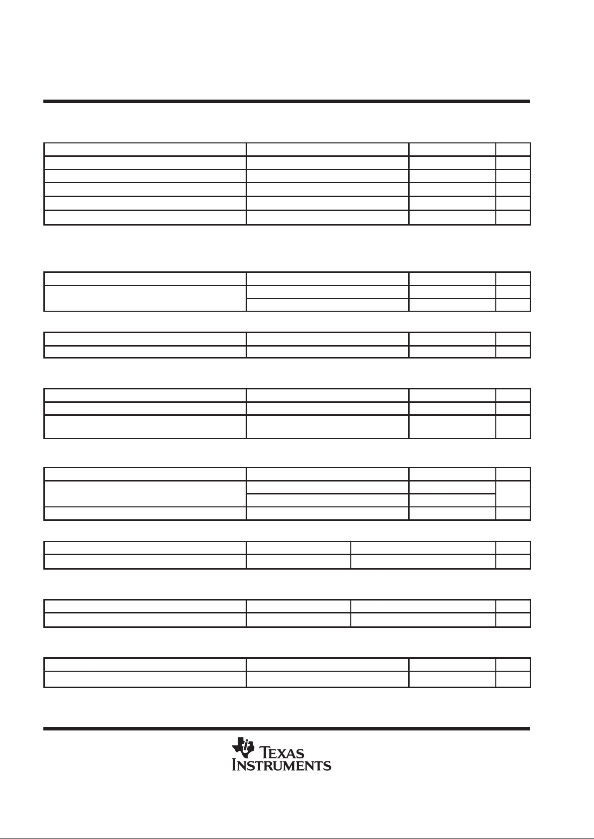
electrical characteristics, TC = 25°C, V
CC
= 24V (unless otherwise noted) (continued)
digital filter f
(s)
RC oscillator
PARAMETER TEST CONDITIONS MIN TYP MAX UNIT
V
ref(RT)
RT reference voltage I
(RT)
= –160 µA 0.19 V
DD
0.2 V
DD
0.21 V
DD
V
V
IT+(CT)
CT upper threshold voltage 0.7 V
DD
V
V
IT–(CT)
CT lower threshold voltage 0.3 V
DD
V
V
(CT)
CT amplitude 1.9 2 2.1 V
I
(CT)
CT charge/discharge current Measured at V
IT+(CT)
and V
IT–(CT)
1.8 I
(RT)
±2 I
(RT)
2.2 I
(RT)
A
lock detection timer
PARAMETER TEST CONDITIONS MIN TYP MAX UNIT
V
IT+(CLT)
CLT upper threshold voltage 0.7 V
DD
V
V
IT–(CLT)
CLT lower threshold voltage 0.3 V
DD
V
V
(CLT)
CLT amplitude 1.9 2 2.1 V
I
(CLT)
CLT charge/discharge current
Measured at VIT +
(CLT)
and V
IT–(CLT)
1.9 I
(RT)
±2 I
(RT)
2.3 I
(RT)
A
high side gate drive
PARAMETER TEST CONDITIONS MIN TYP MAX UNIT
V
C
Clamp voltage
UGX to PHX, I
(UGX)
= –100 µA
14 16 19 V
V
DS(UGX)
Source voltage drop
I
(UGX)
=–10 mA, VCP = VCC + 17 V,
Measure VCP – V
(UGX),VCC
= 18 V
1 1.2 V
Vsink
(UGX)
Sink voltage drop @10 mA
I
(UGX)
=10 mA, V
(PHx)
= 0,
Measure V
(UGX)
– V
(PHx) ,VCC
= 18 V
1.8 2 V
Vsink
(UGX)
Sink voltage drop @100 uA
I
(UGX)
=10 mA, V
(PHx)
= 0,
Measure V
(UGX)
– V
(PHx) ,VCC
= 18 V
0.56 0.7 V
low side gate drive
PARAMETER TEST CONDITIONS MIN TYP MAX UNIT
p
VCC = 18 to 28 V, I
(LGX)
= 0 14 16 19 V
V
O(REG15)
High level output voltage
VCC = 8 to 18 V, I
(LGX)
= 0 7.9 8 18 V
V
source(LGX)
Source voltage
I
(LGX)
= –10 mA, with respect to PGND,
VCC = 18 V
12 14.5 V
V
DS(LGX)
Sink voltage drop
I
(LGX)
= 10 mA, with respect to PGND,
VCC = 18 V
0.6 1 V
current limit control
PARAMETER TEST CONDITIONS MIN TYP MAX UNIT
V
IT(lim)
Limit threshold voltage VCC – V
(SENSE)
0.46 0.5 0.54 V
over-current shutdown control
PARAMETER TEST CONDITIONS MIN TYP MAX UNIT
V
IT(ocsd)
Detection threshold voltage VCC – V
(SENSE)
0.9 1 1.1 V
EEPROM programming
PARAMETER TEST CONDITIONS MIN TYP MAX UNIT
V
PP
VPP programming voltage 12 13 15 V
R
(VPP)
VPP pulldown resistance VPP = 1 V 15 23 35 kΩ
TPIC43T01, TPIC43T02
THREE-PHASE BRUSHLESS MOTOR RPM CONTROLLERS
SLIS098 – APRIL 2000
8
POST OFFICE BOX 655303 • DALLAS, TEXAS 75265
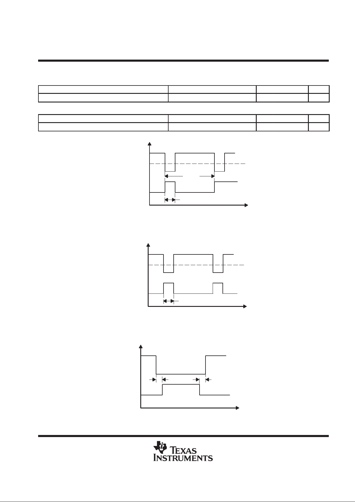
electrical characteristics, TC = 25°C, V
CC
= 24V (unless otherwise noted) (continued)
digital input pins
PARAMETER TEST CONDITIONS MIN TYP MAX UNIT
V
IH
Digital input high level input voltage Interface from 3.3 V controller 2.2 V
V
IL
Digital input low level input voltage Interface from 3.3 V controller 1.1 V
I
(pullup)
Digital input pullup current, S/S, FSEL VIN = 2.2 V –9 –14 –18 µA
I
(F/R)
Digital input pulldown current, F/R VIN = 1.1 V 17.5 27 35 µA
I
(TEST)
TEST input pulldown current VIN = 1.1 V 130 200 250 µA
switching characteristics, T
C
= 25°C, VCC = 24 V
charge pump
PARAMETER TEST CONDITIONS MIN TYP MAX UNIT
180 kHz
f
(CP)
Switching frequenc
y
TC = 0 to 70°C 140 220 kHz
FG signal conditioning
PARAMETER TEST CONDITIONS MIN TYP MAX UNIT
BW Gain bandwidth (see Note 2) 200 kHz
NOTE 2. Design target only. Not tested in production.
FG reference crystal oscillator
PARAMETER TEST CONDITIONS MIN TYP MAX UNIT
f
(OSC)
Crystal frequency range (see Note 2) 5 6.87 10 MHz
f
(OSC1)
OSC1 frequency range
OSC1 driven externally, see FG Reference
Oscillator section
1 10 MHz
NOTE 2. Design target only. Not tested in production.
PWM control
PARAMETER TEST CONDITIONS MIN TYP MAX UNIT
22.7
f
(PWM)
PWM frequenc
y
TC = 0 to 70°C
18 27
kH
z
t
(DT)
Gate drive dead time control See Figure 3 1 3.2 µs
digital filter f
(s)
RC oscillator
PARAMETER TEST CONDITIONS MIN TYP MAX UNIT
f
(CT)
Oscillator frequency (see Note 2) 1/(2 × RT × CT) ±10% Hz
NOTE 2. Design target only. Not tested in production.
lock detection timer
PARAMETER TEST CONDITIONS MIN TYP MAX UNIT
f
(CLT)
CLT oscillator frequency (see Note 2) 1/(2 × RT × CLT) ±10% Hz
NOTE 2. Design target only. Not tested in production.
lock detection
PARAMETER TEST CONDITIONS MIN TYP MAX UNIT
LD
ERR
†
Lock detect threshold ±5 %
†
Non JEDEC symbol.
TPIC43T01, TPIC43T02
THREE-PHASE BRUSHLESS MOTOR RPM CONTROLLERS
SLIS098 – APRIL 2000
9
POST OFFICE BOX 655303 • DALLAS, TEXAS 75265
switching characteristics, T
C
= 25°C, VCC = 24 V (continued)
current limit control
PARAMETER TEST CONDITIONS MIN TYP MAX UNIT
t
(DG)
Deglitch blanking time V
(SENSE)
– VL ≥ 100 mV, See Figure 1 0.5 3.7 6.5 µs
over-current shutdown control
PARAMETER TEST CONDITIONS MIN TYP MAX UNIT
t
(OCSD)
Response time See Figure 2 0.5 1.5 2.5 µs
High-Side Gate
Output
PWM
Cycle
t
(DG)
Amplitude
time
V
CC
V
L
V
(SENSE)
Figure 1. Current Limit Deglitch Blanking Time
High-Side Gate
Output
t
(OCSD)
Amplitude
time
V
CC
V
OCSD
V
(SENSE)
Figure 2. Over-Current Shutdown Response Time
Amplitude
time
UGx
t
(DT)
LGx
t
(DT)
Figure 3. Gate Drive Deadtime
 Loading...