

TPIC2101
DC BRUSH MOTOR CONTROLLER
SLIS060 – OCTOBER 1995
D
0 V to16 V, 50 mA Max PWM Gate Drive
Output
D
Dual Speed Command Input Capability
D
Effective Motor Voltage Adjustment
D
100% Duty Cycle Capability
D
Low Current (<200 µA) Sleep State
D
Built-in Soft Start
D
Over/Under V oltage Protection
D
Over Current Protection of External
FET/IGBT
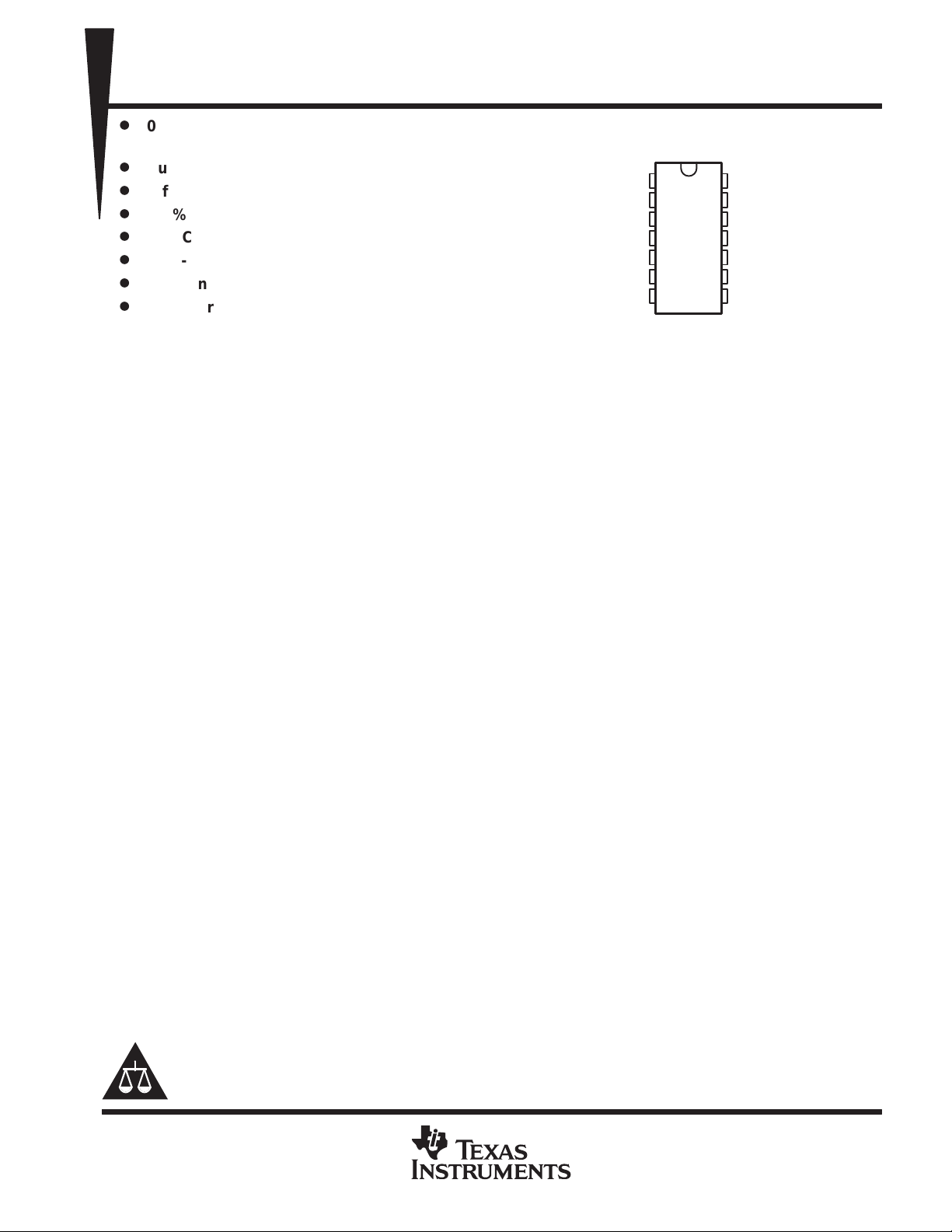
D or N PACKAGE
V5P5
MAN
AUTO
SPEED
ROSC
COSC
INT
(TOP VIEW)
1
14
2
13
3
12
4
11
5
10
6
7
9
8
CCS
AREF
V
bat
GD
GND
ILS
ILR
description
The TPIC2101 is a monolithic integrated control circuit designed for direct current (dc) brush motor control that
generates a user-adjustable, fixed-frequency, variable duty cycle, pulse width modulated (PWM) signal
primarily to control rotor speed of a permanent magnet dc motor. The TPIC2101 can also be used to control
power to other loads such as solenoids and incandescent bulbs. This device drives the gate of an external, low
side NMOS power transistor to provide PWM controlled power to a motor or other loads. Inductive current from
motor or solenoid loads during PWM off-time is recirculated through an external diode.
The TPIC2101 accepts a 0% to 100% PWM signal (auto mode) or a 0 V to 2.2 V differential voltage (manual
mode), and internally engages the correct operating mode to accept the input type.
The device operates in a sleep state, a run state, or a fault state. In the sleep state the gate-drive (GD) terminal
is held low and the overall current draw is less than 200 µA. The normal operating mode of the device is in the
run state and is initiated by any speed command. When the device detects an overvoltage or current fault, it
enters the fault state.
The TPIC2101 is offered in a 14-terminal plastic DIP (N) package, and a SOIC (D) package, and is characterized
for operation over the operating free-air temperature range of –40°C to 105°C.
Please be aware that an important notice concerning availability, standard warranty, and use in critical applications of
Texas Instruments semiconductor products and disclaimers thereto appears at the end of this data sheet.
PRODUCTION DATA information is current as of publication date.
Products conform to specifications per the terms of Texas Instruments
standard warranty. Production processing does not necessarily include
testing of all parameters.
POST OFFICE BOX 655303 • DALLAS, TEXAS 75265
POST OFFICE BOX 1443
• HOUSTON, TEXAS 77251–1443
Copyright 1995, Texas Instruments Incorporated
1
TPIC2101
DC BRUSH MOTOR CONTROLLER
SLIS060 – OCTOBER 1995
functional block diagram
V5P5
Sleep
AUTO and MAN
Logic
Sleep AREF 20 kHz
Oscillator and
Voltage Ramp
Waveform Generator
MAN
AUTO
CCS
V5P5
2
AUTO and MAN
Input Config
3
I
CCS
CCS
14
Buffer
1
V
bat
Bandgap
Buffer
Sleep
AREF
V5P5
V
bat
+
_
MDET
V
bat
+
_
V5P5
V
bat
2×
Bandgap
and IBIAS
ADET
UVSD
20 kHz
20 kHz
Source
Select
Sleep
SPEED INT
47
V7
AREF
_
+
V
trip
V
ramp
V
bat/4
AREF
PWMout
V
bat
Switched
V
bat
AREF
20 kHz
ILimit
Logic
IDET GDDIS
Sleep OVSD
V
bat/8
V5P5
GD
Logic
AREF
OVSD
IFLT
UVSD
AREF
V5P5
V5P5
UVSD
Gate
Drive
8
ILR
9
ILS
12
V
bat
11
GD
10
GND
13 5 6
AREF ROSC COSC
NOTE A: For correct operation, no terminal may be taken below GND.
2
POST OFFICE BOX 655303 • DALLAS, TEXAS 75265
POST OFFICE BOX 1443
• HOUSTON, TEXAS 77251–1443
I/O
DESCRIPTION
DESCRIPTION
TPIC2101
DC BRUSH MOTOR CONTROLLER
SLIS060 – OCTOBER 1995
Terminal Functions
TERMINAL
NAME NO.
V5P5 1 O 5.5 V supply voltage. V5P5 is a regulated voltage supply from V
MAN 2 I Manual control input. MAN is an active high (greater than 5.5 V asserts the manual mode) input that serves
AUTO 3 I PWM control input. AUTO is an active low input that remains active if pulsed every 2048 counts of the
SPEED 4 O Integrator output. SPEED is an integrator output with a required minimum resistance between SPEED and
ROSC 5 O Oscillator resistor output. ROSC has an external resistor connected to ground which determines the
COSC 6 O Oscillator capacitor output. COSC has an external capacitor connected to ground which determines (with
INT 7 I Integrator input. INT is an input from an integrator that requires a 4.7 µF capacitor and a 20 k minimum
ILR 8 I Current limit reference. ILR is an input from a resistor divider off AREF.
ILS 9 I Current limit sense. ILS senses drain voltage of external FET. ILS trips within ±10 mV of ILR.
GND 10 Ground terminal
GD 11 O Gate drive output. GD, PWM output, 0-V
V
bat
AREF 13 O 5.5 V reference voltage. AREF is a 5.5 V reference voltage switched from V5P5 during the run state. AREF
CCS 14 Constant current sink. I
12 I Positive power input.
run state. This requires a 4.7 µF tantalum capacitor from V5P5 to GND for stability.
as a positive differential input (0-2.3 V full range) for the manual mode. In man mode, I
oscillator frequency. It also serves as a negative differential input for the manual mode. In auto mode, I
is approx. 13×Iccs pullup, I
INT terminals of 20 kΩ (typically 1 second RC time constant, or as required for soft start).
constant charging current of COSC. The IC forces a voltage of V
ROSC) switching frequency. f(osc) = 2/(ROSC×COSC)
resistance between the SPEED and INT terminals.
FET .
is used as a reference for ILR in current limit detection and is capable of sourcing 2 mA of current.
is approx. 20×I
auto
equals AREF/(2×R
CCS
pulldown in man mode.
ccs
voltage, provides a 0-V
bat
). Requires an external resistor.
ccs
, internally switched to AREF during the
bat
is approx. 20×I
man
/4 in run state.
bat
PWM output pre-drive for an external
bat
ccs
auto
.
recommended external components for auto and manual modes (see Figures 2 and 4)
TERMINAL
NAME NO.
V5P5 1 Capacitor – 4.7 µF tantalum
MAN 2 Capacitor – 0.1 µF
MAN 2 Resistor – 499 Ω, 1%, 100 ppm
AUTO 3 Capacitor – 0.47 µF
AUTO 3 Resistor – 499 Ω, 1%, 100 ppm
SPEED 4 Resistor – 100 kΩ, 1%, 100 ppm to INT terminal, (minimum 20 kΩ)
ROSC 5 Resistor – 45.3 kΩ
COSC 6 Capacitor – 2200 pF
INT 7 Capacitor – 4.7 µF
CCS 14 Resistor – 27.4 kΩ, 1%, 100 ppm
POST OFFICE BOX 655303 • DALLAS, TEXAS 75265
POST OFFICE BOX 1443
• HOUSTON, TEXAS 77251–1443
3

TPIC2101
DC BRUSH MOTOR CONTROLLER
SLIS060 – OCTOBER 1995
detailed description
The TPIC2101 is an integrated circuit that generates a fixed frequency , variable duty cycle PWM signal to control
the rotor speed of a permanent-magnet dc motor. This section provides a functional description of the device.
dual command speed input capability
The TPIC2101 is user configurable to either auto or manual mode, and can sense either configuration internal
to the IC. In automatic mode, the speed-command-signal is an open-collector PWM signal on the AUTO
terminal, and the MAN terminal is floating. In manual mode, the speed-command-signal is a variable resistance
across the AUTO and MAN terminals with the MAN terminal connected to V
sleep, run, and fault states
The TPIC2101 operates in a sleep state, a run state, or a fault state. In the auto mode, a zero-speed input
initiates the sleep state. In the manual mode, an open-circuit at the AUTO and MAN terminals initiates the sleep
state. The device will also be in the sleep state during fault conditions. In the sleep state, the gate drive terminal
(GD) is held low and the overall current draw is less than 200 µA. Any speed command initiates the run state,
which is the normal operating state of the device. The fault state is entered only when the device detects an
overvoltage or current fault. Fault state is exited either by removal of the overvoltage condition (exiting to run
state) or by resetting a current fault by entering the sleep state.
speed command adjustment
bat
.
The device adjusts the GD terminal PWM signal with changes in V
to keep the effective motor voltage
bat
constant. The effective motor voltage is defined to be the product of the GD terminal PWM rate and the voltage
of V
. Figure 1 shows motor voltage as a function of input speed command in the automatic mode for various
bat
battery voltages. PWM
is described as the duty cycle of the PWM signal at the AUTO terminal.
in
16
14
12
V
= 12
bat
10
8
6
Motor Voltage – V
4
2
0
V
= 8
bat
0204060
PWMin– Incoming Pulse Width Modulation – %
V
= 16
bat
80 100
Figure 1. Motor Voltage vs. Incoming PWM for Various Battery Voltages
over/under voltage protection
The IC enters the fault state if V
below the under-voltage shutdown (V
rises above over-voltage shutdown (V
bat
typically equals 7.5 volts) the IC enters sleep state. Hysteresis assures
UV
that the device will not toggle into and out of sleep state or fault condition.
4
POST OFFICE BOX 655303 • DALLAS, TEXAS 75265
POST OFFICE BOX 1443
• HOUSTON, TEXAS 77251–1443
typically equals 18.5 V). If V
OV
bat
falls
DC BRUSH MOTOR CONTROLLER
SLIS060 – OCTOBER 1995
current limit protection
Current through the motor is limited by lowering the GD terminal PWM when a high current situation occurs.
If the condition persists, the device shuts off the gate drive (GD terminal) until the circuit is reset externally by
entering the sleep state.
theory of operation
This section explains the normal circuit operation for the automatic and manual states.
power supply and oscillator
TPIC2101
Positive voltage is supplied to the integrated circuit on the V
steps down the V
supply to the regulated 5.5 V supply at the V5P5 terminal. AREF is shorted to V5P5 in run
bat
terminal, ground is the GND terminal. The IC
bat
state and disconnected when the IC is in sleep state. Two terminal connections (COSC and ROSC) are provided
to control an internal oscillator. The oscillator freq, f
f
(osc)
+
ROSC COSC
2
, is defined by the following equation:
(osc)
Nominal oscillator frequency is 20-kHz based on the recommended components.
automatic mode signal decoding
In automatic state, a high-to-low signal transition on the AUTO terminal (open collector) will wake the device
from the sleep state into the run state. The speed command information is contained in the duty cycle of a 100 Hz
PWM signal on the same terminal. The speed information is inverted, i.e. a signal that is 10% high commands
a faster speed than a 20% high signal. In automatic mode the MAN terminal is floating. The device is capable
of rejecting ± 2 V of ground offset V
between the open-collector switching transistor and the GND terminal
IO
without affecting the output duty cycle. Two terminals are provided for an RC integrator (SPEED and INT) to
average the incoming PWM signal for use as a PWM comparator input. Figure 2 illustrates the automatic state
connections.
No Connection
V
IO
499 Ω
499 Ω
2
3
I = 100 µA
MAN
TPIC2101
AUTO
CCS SPEED INT
14 2.75 V 4 7
20 kΩ min
27.4 kΩ
4.7 µF
Figure 2. Automatic Mode Connections
POST OFFICE BOX 655303 • DALLAS, TEXAS 75265
POST OFFICE BOX 1443
• HOUSTON, TEXAS 77251–1443
5

TPIC2101
DC BRUSH MOTOR CONTROLLER
SLIS060 – OCTOBER 1995
automatic mode signal decoding (continued)
The device enters the sleep state if the PWM signal on the AUTO terminal is absent (the AUTO terminal remains
high or low) for 2048 clock cycles of the 20 KHz oscillator. An internal 1 mA pull-up resistor is provided for the
AUTO terminal when in the auto mode. This pull-up resistor is not present in the manual mode or during sleep
state.
The device adjusts the output PWM duty cycle to keep the effective motor voltage constant with changing battery
voltages (V
) as per the equation:
bat
PWM
(2.88)13.12(1*Input Duty Cycle))
+
out
V
bat
100%
Figure 3 illustrates this transfer curve with various battery voltages.
100
V
= 12
90
80
70
60
50
– Output PWM – %
40
out
30
PWM
20
10
0
0 102030405060
V
= 16
bat
PWMin – Incoming Pulse Width Modulation – %
bat
V
bat
70 80 90 100
Figure 3. Output PWM vs. Incoming PWM for Various Battery Voltages
= 8
The allowable automatic mode PWM
variation is ± 7% over all operating conditions as indicated in the AC
out
characteristics Table.
manual mode speed signal decoding
In manual mode, a high input (>5.5V) on the MAN terminal changes the state of the device from sleep to run.
While in the run state the device senses the resistance between the MAN and AUTO terminals by turning on
a 2 mA current sink to each terminal. The MAN and AUTO current sinks are multiplied 20 X from the CCS current.
This 2 mA current sink creates a 1 V drop across each 0.5 kΩ resistor and a 0 to 2.2 V differential across the
0 to 1 kΩ potentiometer (and thus across the 2 terminals). The SPEED and INT terminals should be utilized as
in the proceeding section as a low-pass filter. When the connection to the MAN terminal is opened, the device
enters the sleep state. In addition, the device is capable of rejecting up to 2.2 V of source voltage offset (V
as indicated in Figure 4.
6
POST OFFICE BOX 655303 • DALLAS, TEXAS 75265
POST OFFICE BOX 1443
• HOUSTON, TEXAS 77251–1443
IO
),

manual mode speed signal decoding (continued)
47 Ω
V
IO
TPIC2101
DC BRUSH MOTOR CONTROLLER
SLIS060 – OCTOBER 1995
Battery
Enable
Switch
1 kΩ
pot
499 Ω
499 Ω
I = 100 µA
V
bat
2
MAN
TPIC2101
3
AUTO
CCS SPEED INT
14 2.75 V 4 7
20 kΩ min
27.4 kΩ
4.7 µF
Figure 4. Manual Mode Connections
As in the automatic mode, the device will adjust the GD terminal PWM duty cycle to keep the effective motor
voltage constant with changing battery voltages (V
PWM
out
+
(2.88)6.56(V
MAN
V
bat
*
V
AUTO
))
100%
). The transfer equation for the manual mode is:
bat
Figure 5 shows the output characteristic for various source voltages.
100
90
80
70
60
50
40
30
– Manual Mode Output PWM – %
out
20
PWM
10
0
0 0.2 0.4 0.6 0.8 1 1.2
Figure 5. Manual Mode Input Signal vs. Output PWM
The allowable manual mode PWM
characteristics table.
V
= 16
bat
V
= 12
bat
V
= 8
bat
1.4 1.6 1.8 2
V
- V
MAN
variation is ±7% over all operating conditions as indicated in the AC
out
– Differential Voltage – V
AUTO
POST OFFICE BOX 655303 • DALLAS, TEXAS 75265
POST OFFICE BOX 1443
• HOUSTON, TEXAS 77251–1443
7

TPIC2101
DC BRUSH MOTOR CONTROLLER
SLIS060 – OCTOBER 1995
over/under voltage operating
The TPIC2101 detects an over or under voltage condition (on the V
terminal) and turns off the gate drive
bat
circuit. The device remains in this condition until the supply voltage returns to normal operating voltage.
Hysteresis assures that the over/under voltage condition does not toggle off and on near the threshold. The INT
terminal pulls toward GND through an internal impedance of less than 500 Ω during the over-voltage condition
or during sleep state. This ensures a slow ramp up of the GD terminal PWM when the V
voltage returns to
bat
the operating range.
current limit operation
An over-current condition is detected if the ILS terminal is higher than the ILR terminal while the gate drive (GD
terminal) is high. This condition activates a closed-loop control, causing the INT terminal to be pulled low
(through an internal resistance less than 500 Ω) lowering the commanded duty cycle to close the loop.
current fault operation
During a window of 8192 clock cycles, a latch is set if at least once during the window, a current limit condition
is detected. If a current limit condition is set for eight consecutive 8192 clock cycle windows, the gate drive (GD
terminal) will be shut off for a disable period of 65536 clock cycles. During the disable period, the INT terminal
is pulled to GND through an internal resistance of less than 500 Ω. After the disable period is completed, an
internal restart is attempted. If the current limit is present again, as described above, for 8 consecutive windows,
the GD and INT terminals are again pulled to GND and the device remains in this current fault state until the
device is cycled through a sleep state to run state. However, if the current limit condition is not present during
any of the eight 8192 clock cycle windows, the latches for the 8 count window timer and the two cycle
shutdown/restart are reset. See timing diagrams, Figures 6, 7, and 8.
absolute maximum ratings over the operating free-air temperature range (unless otherwise
noted)
†
‡
†
‡
Supply voltage range, V
–0.3 V to 40 V. . . . . . . . . . . . . . . . . . . . . . . . . . . . . . . . . . . . . . . . . . . . . . . . . . . . . . . .
bat
Input voltage range, MAN, AUTO –0.3 V to 40 V. . . . . . . . . . . . . . . . . . . . . . . . . . . . . . . . . . . . . . . . . . . . . . . . . . .
Input voltage range, INT
Continuous gate drive output current, I
Continuous speed output current, I
Continuous output current, I
Continuous ROSC output Current, I
Continuous output current, I
Thermal Resistance, junction to ambient, R
CCS
ILR –0.3 V to 7 V. . . . . . . . . . . . . . . . . . . . . . . . . . . . . . . . . . . . . . . . . . . . . . . . . . .
,
O(SPEED)
O(V5P5)
O(CCS)
±50 mA. . . . . . . . . . . . . . . . . . . . . . . . . . . . . . . . . . . . . . . . . . . . . . . . . .
GD
±1 mA. . . . . . . . . . . . . . . . . . . . . . . . . . . . . . . . . . . . . . . . . . . . . . . .
, I
O(AREF)
O(ROSC)
20 mA. . . . . . . . . . . . . . . . . . . . . . . . . . . . . . . . . . . . . . . . . . . . . .
1 mA. . . . . . . . . . . . . . . . . . . . . . . . . . . . . . . . . . . . . . . . . . . . . . . . .
500 µA. . . . . . . . . . . . . . . . . . . . . . . . . . . . . . . . . . . . . . . . . . . . . . . . . . . . . . .
: D package 131°C/W. . . . . . . . . . . . . . . . . . . . . . . . . . . . . . . .
ΘJA
N package 78°C/W. . . . . . . . . . . . . . . . . . . . . . . . . . . . . . . . . .
Operating free-air termperature range, T
Maximum junction temperature, T
Storage temperature range, T
Stresses beyond those listed under “absolute maximum ratings” may cause permanent damage to the device. These are stress ratings only, and
functional operation of the device at these or any other conditions beyond those indicated under “recommended operating conditions” is not
implied. Exposure to absolute-maximum-rated conditions for extended periods may affect device reliability.
Under load dump conditions, the voltage on V
JM
–65°C to 150°C. . . . . . . . . . . . . . . . . . . . . . . . . . . . . . . . . . . . . . . . . . . . . . . . . .
stg
bat
–40°C to 105°C. . . . . . . . . . . . . . . . . . . . . . . . . . . . . . . . . . . . . . . . . .
A
150°C. . . . . . . . . . . . . . . . . . . . . . . . . . . . . . . . . . . . . . . . . . . . . . . . . . . . . . .
can reach 40 V within 1 ms.
8
POST OFFICE BOX 655303 • DALLAS, TEXAS 75265
POST OFFICE BOX 1443
• HOUSTON, TEXAS 77251–1443

TPIC2101
DC BRUSH MOTOR CONTROLLER
SLIS060 – OCTOBER 1995
recommended operating conditions
MIN NOM MAX UNIT
Supply voltage, V
AREF Input current I
Input voltage, V
Differential voltage, V
Input voltage, V
VI, ILR, ILS 0.5 2.75 V
Output resistance, input resistance, R
Output Resistance, ROSC, r
Output Capacitance, COSC, C
Gate drive frequency f = 2/(ROSC × COSC), f
Gate drive output capacitance, C
Operating free-air temperature, T
bat
(AREF)
I(MAN), VI(AUTO)
I(MAN)
(auto mode) 0 5.5 V
I(AUTO)
(manual mode) 6 16 V
– V
I(AUTO)
(CCS)
o
O
(GD)
O(GD)
A
8 12 16 V
0 2 mA
0 2.2 V
27.2 27.5 27.8 kΩ
20 100 kΩ
1 5 nF
20 kHz
3300 pF
–40 105 °C
POST OFFICE BOX 655303 • DALLAS, TEXAS 75265
POST OFFICE BOX 1443
• HOUSTON, TEXAS 77251–1443
9

TPIC2101
I
Quiescent current (sleep state), V
DC BRUSH MOTOR CONTROLLER
SLIS060 – OCTOBER 1995
electrical characteristics, V
PARAMETER TEST CONDITION MIN TYP MAX UNIT
I
bat
bat(Q)
V
(AREF)
V
IO
I
IB
I
IO
I
OL(CLS)
V
IL(AUTO)
V
IH(AUTO)
I
I(AUTO)
I
I(AUTOQ)
V
IH(MAN)
V
IL(MAN)
V
ID(MAN)
†
Indicates electrical parameter not tested in production.
Supply current (average), V
Voltage supply regulation, AREF
Input offset voltage, current limit
comparator, ILS, ILR
Input bias current, current limit comparator,
†,
ILS, ILR
Input offset current, current limit comparator,
†
ILS, ILR
Pulldown current, ILS terminal
blanking, ILS
Automatic mode low level input
voltage, AUTO
Automatic mode high level input
voltage, AUTO
Input current, automatic mode, AUTO
Input current, auto sleep mode, AUTO
High level input voltage, manual mode, MAN
Low level input voltage, manual mode, MAN
Input voltage, manual mode high differential
(high speed command), MAN-AUTO
= 8 V to 16 V, T
bat
bat V
p
bat
= 25°C
A
V
= 16 V, GD open,
bat
f(osc) = 20 kHz,
MAN = AUTO =V
= 16 V, GD open,
bat
f(osc) = 20 kHz, MAN open,
Auto mode,
AUTO – 99% PWM
V
= 13 V,
bat
AUTO and MAN open
V
= 13 V,
bat
AUTO shorted to MAN, floating
I
= 0 – 2 mA,
(AREF)
MAN = AUTO = V
AUTO or MAN mode, ILS,
ILR common mode,
Voltage range 0.5 – 2.75 V,
V
= 4.5 V,
int
Detect I
(int)
ILS, ILR common mode,
Voltage range 0.5 – 2.75 V
ILS, ILR common mode,
Voltage range 0.5 – 2.75 V
ILS = 100 mV ,
GD commanded low
MAN open, AUTO mode,
Lower V
I(AUTO)
MAN open, AUTO mode,
Raise V
I(AUTO)
MAN open, Auto mode,
V
I(AUTO)
MAN open, Sleep state,
V
I(AUTO)
V
= 9 V to 16 V,
bat
V
IH(MAN)
Raise V
(MAN)
V
Lower V
V
V
=VI(
I(MAN)
I(MAN)
= 16 V,
bat
–3.5 V < MAN < V
bat
> 100 µA
= 0 V
= 0 V
= V
IH(AUTO)
until V
AUTO)
until V
bat
in
bat
until V
until V
I(SPEED)
I(SPEED)
,
I(AREF)
,
I(AREF)
bat
>2.4V
< 2.4 V
> 2.5 V
< 2.5 V
4 10 mA
2 10 mA
150 200 µA
165 200 µA
5.225 5.5 5.775 V
10 mV
250 nA
100 nA
250 360 µA
2.7 3 3.3 V
3.6 4 4.4 V
–1 –10 mA
–40 –80 µA
5 5.5 6 V
2.3 2.5 2.7 V
1.7 2.3 V
10
POST OFFICE BOX 655303 • DALLAS, TEXAS 75265
POST OFFICE BOX 1443
• HOUSTON, TEXAS 77251–1443

V
gg,g
V
g,g
TPIC2101
DC BRUSH MOTOR CONTROLLER
SLIS060 – OCTOBER 1995
electrical characteristics, V
PARAMETER TEST CONDITION MIN TYP MAX UNIT
Input voltage, manual mode
V
ID(low)
I
I(MAN)
I
I(AUTO)
I
I(MANRATIO)
I
I(MAN(a))
I
I(MANQ)
V
(CCS)
V
(OV)
V
hys(OV)
V
IT-(UVLO)
V
IT+(UVHI)
V
hys(UV)
OH(GD)
OL(GD)
V
GD(SL)
I
(GDP)
I
(INT)
low differential (low speed
command), MAN–AUTO
Input currents, auto and
manual mode, MAN, AUTO
Input current, manual mode
matching ratio, MAN, AUTO
Input current, man terminal
auto mode, MAN
Input current, man terminal
sleep mode, MAN
Constant current sink voltage
regulation, CCS
Over voltage shutdown, V
Hysteresis, over voltage, V
Under voltage shutdown
negative going threshold
voltage, V
Under voltage shutdown
positive going threshold
voltage, V
Hysteresis, under voltage, V
High level output voltage, gate
drive, GD
Low level output voltage, gate
drive, GD
Gate voltage, sleep-state, GD Sleep state, IGD = 2 mA 0.03 0.75 V
Pulldown current, gate drive
passive, GD
Pulldown current, INT
bat
bat
= 8 V to 16 V, T
bat
V
bat
where “∆” is the lesser of 2 V and 16 V –V
PWM
V
I(DIFF)
V
bat
where “∆” is the lesser of 2 V and 16 V –V
MAN – AUTO = 0 V to 2 V,
R
(css)
V
bat
where “∆” is the lesser of 2 V and 16 V –V
MAN – AUTO = 0 V to 2 V,
R
css
Auto mode, MAN = 2.2 V 5 10 15 µA
Sleep state, MAN = 2.2 V 5 10 15 µA
Auto or Man mode, I
V
bat
bat
bat
Detect I
V
bat
Detect I
MAN = V
Detect AREF < 2.5 V
MAN = V
Detect AREF > 2.5 V
batV(UVHI)
IGD = –50 mA, INT = 4.5 V,
Run state
IGD = –2 mA, INT = 4.5 V,
Run state
Run state, IGR = 50 mA,
V
I(INT)
Run state, IGD = 2 mA,
INT = 0 V, V
V
bat
Run state, V
V
I(INT)
= 25°C (continued)
A
–3.5 V < MAN < V
@ V
out
(diff)
= 0 V
–3.5 V < MAN < V
= 27.5 kΩ to GND
–3.5 V < MAN < V
= 27.5 kΩ to GND
rising from 16 V, INT = 1 V ,
> 100 µA
(INT)
rising from 20.1 V, INT = 1 V,
< 100 µA
(INT)
, V
bat
,V
bat
– V
(UVLO)
= 0 V, V
open, VGD = 0.75 V 7.5 20 µA
= 1 V
+∆V
bat
= 0.2 V ≥ PWM
+∆V
bat
+∆V
bat
(CCS)
falling from 9 V ,
bat
rising from 6.9 V,
bat
COSC
COSC
> V
ILS
,
bat
@
out
,
bat
,
bat
= –100 µA 2.58 2.78 2.92 V
= 1 V
= 1 V
,
ILR
1.70 2 2.30 mA
–7 7 %
17 18.5 20 V
0.5 0.8 0.99 V
7 7.5 8 V
8 8.5 9 V
0.5 1 V
V
–3 V
bat
V
–0.2 V
bat
2 3 mA
0.2 V
bat
bat
3.5 V
0.75 V
V
V
POST OFFICE BOX 655303 • DALLAS, TEXAS 75265
POST OFFICE BOX 1443
• HOUSTON, TEXAS 77251–1443
11

TPIC2101
DC BRUSH MOTOR CONTROLLER
SLIS060 – OCTOBER 1995
switching characteristics, V
PARAMETER TEST CONDITIONS MIN TYP MAX UNIT
t
r
t
f
f
(osc)
Rise time
Fall time
Output PWM absolute
accuracy to spec equation
Oscillator frequency ROSC = 45.3 kΩ, COSC = 2200 pF 19 20 21 kHz
Minimum speed pedestal
PARAMETER MEASUREMENT INFORMATION
Time Block 1 Time Block 2 Time Block 3 Time Block 4 Time Block 5
Internal
Clock
ILS>ILR ?
1 = Yes, 0 = No
8192 Cycles 8192 Cycles 8192 Cycles 8192 Cycles 8192 Cycles
= 8 V to 16 V, T
bat
V
bat
ROSC = 45.3 kΩ, COSC = 2200 pF
V
bat
ROSC = 45.3 kΩ, COSC = 2200 pF
16 > V
GD open,
Measure at GD = 0.5 × V
MAN = AUTO=V
V
bat
AUTO @ 99% duty cycle
= 25°C
A
= 16 V, Load = 3300 pF,
= 16 V, Load = 3300 pF,
> 9 Manual and automatic modes
bat
@ 20 kHz
bat
= 16 15 21 %DC
bat
= 16, MAN floating,
1 µs
0.8 µs
–7% 7%
15 21 %DC
GD Terminal
INT Terminal
Through 500 Ω
Internal Latch
or Counter
Current Fault
Latch/Counter
Disable Latch
123 0
No Current Limit Condition Present in Time Block 4.
Internal Counter or Latch Set to zero. Current Limit
Condition Not Present For Eight Consecutive 8192 Cycles.
No Disable Period.
Figure 6. Current Fault Timing Diagram, Normal State
12
POST OFFICE BOX 655303 • DALLAS, TEXAS 75265
POST OFFICE BOX 1443
• HOUSTON, TEXAS 77251–1443

TPIC2101
DC BRUSH MOTOR CONTROLLER
SLIS060 – OCTOBER 1995
PARAMETER MEASUREMENT INFORMATION
Time
Block 1
Internal
Clock
ILS>ILR ?
1 = Yes, 0 = No
GD Terminal
INT Terminal
Through 500 Ω
Internal Latch
or Counter
Current Fault
Latch/Counter
Disable Latch
Time Block Repeated Six Times
Current Limit for Eight Consecutive Time Blocks.
Disable Output for 65536 Clock Cycles.
8192
Cycles
18012
Time
Block 8
8192
Cycles
65536 Cycles
Restart Attempted
No Current Limit Condition in Time Block 19.
Time
Block 17
8192
Cycles
Internal Latch or Counter Reset to Zero.
Time
Block 18
8192
Cycles
Restart Successful
Block 19
Cycles
Time
8192
0
Figure 7. Current Fault Timing Diagram, Over-Current Limit Condition
POST OFFICE BOX 655303 • DALLAS, TEXAS 75265
POST OFFICE BOX 1443
• HOUSTON, TEXAS 77251–1443
13

TPIC2101
DC BRUSH MOTOR CONTROLLER
SLIS060 – OCTOBER 1995
PARAMETER MEASUREMENT INFORMATION
Time
Block 1
Internal
Clock
ILS>CLR ?
1 = Yes, 0 = No
GD Terminal
INT Terminal
Through 500 Ω
Internal Latch
or Counter
Current Fault
Latch/Counter
Disable Latch
Time Block Repeated Six Times
Current Limit For Eight Consecutive Time Blocks.
Disable Output For 65536 Clock Cycles.
8192
Cycles
1801 8
Time
Block 8
8192
Cycles
65536 Cycles
Attempted
Block 17
Restart
Time
8192
Cycles
Time BlocK 17
Repeated Six Times
Restart Not Successful.
Enter Current Fault State.
Time
Block 21
8192
Cycles
Time
Block A
8192
Cycles
0
Current Fault State
(see Note A)
NOTE A: The integrated circuit remains in this state until cycled through the sleep state into the run state. Timing resumes as shown in time block
A at right.
Figure 8. Over-Current Fault State Timing Diagram 3
14
POST OFFICE BOX 655303 • DALLAS, TEXAS 75265
POST OFFICE BOX 1443
• HOUSTON, TEXAS 77251–1443

TPIC2101
DC BRUSH MOTOR CONTROLLER
SLIS060 – OCTOBER 1995
TYPICAL CHARACTERISTICS
MANUAL/AUTO CURRENT
vs
CCS CURRENT
5
V
= 12 V
bat
4.5
4
3.5
3
2.5
2
– Manual/Auto Current – mA
1.5
AUTO
I
1
MAN,
0.5
I
0
0 50 100 150 200 250
I
– CCS Current (Manual Mode) – µA
CCS
(MANUAL MODE)
Figure 9 Figure 10
INTEGRATOR PULLDOWN CURRENT
vs
INTEGRATOR INPUT VOLTAGE
18
V
= 12 V
bat
ILS>ILR
15
AUTO CURRENT
vs
CCS CURRENT (AUTO MODE)
–4
V
= 12 V
–3.6
–3.2
–2.8
–2.4
–2
–1.6
– Auto Current – mA
–1.2
AUTO
I
–0.8
–0.4
bat
0
0 –60 –120 –180 –240 –300
I
– CCS Current (Auto Mode) – µA
CCS
OSCILLATOR CAPACITOR CURRENT
vs
OSCILLATOR RESISTOR CURRENT
1000
Aµ
900
800
–40°C
105°C
25°C
12
–40°C
9
6
– Integrator Pulldown Current – mA
3
(INT)
I
0
012345
V
– Integrator Input Voltage – V
(INT)
105°C
25°C
Figure 11 Figure 12
POST OFFICE BOX 655303 • DALLAS, TEXAS 75265
POST OFFICE BOX 1443
700
600
500
400
300
Oscillator Capacitor Current –
–
200
100
(COSC)
I
0
0 40 120 240
I
(ROSC)
• HOUSTON, TEXAS 77251–1443
80 160200 280 360 440480
– Oscillator Resistor Current – µA
320 400 520
15

TPIC2101
DC BRUSH MOTOR CONTROLLER
SLIS060 – OCTOBER 1995
TYPICAL CHARACTERISTICS
GATE DRIVE LOW SIDE
GATE DRIVE CURRENT
1
0.9
0.8
0.7
0.6
0.5
0.4
– Gate Drive Low Side – V
0.3
OL
V
0.2
0.1
0
0 5 10 15 20 25 30
IGD – Gate Drive Current – mA
EFFECTIVE MOTOR VOLTAGE
INCOMING PULSE WIDTH MODULATION
16
14
12
10
8
– Effective Motor Voltage – V
6
GATE DRIVE HIGH SIDE
vs
vs
GATE DRIVE CURRENT
16
105°C
25°C
–40°C
35 40 45 50
14.4
12.8
11.2
9.6
8
6.4
– Gate Drive High Side – V
4.8
OH
V
3.2
1.6
0
05045403530252015105
IGD – Gate Drive Current – mA
Figure 13 Figure 14
MOTOR RPM
V
bat
vs
= 14 V
V
bat
= 16 V
V
bat
V
bat
V
bat
= 10 V
= 8 V
INCOMING PULSE WIDTH MODULATION
2500
2000
= 12 V
1500
1000
Motor RPM – RPM
vs
V
= 14 V
bat
V
bat
V
bat
V
= 8 V
105°C
= 16 V
V
bat
25°C
–40°C
= 12 V
bat
= 10 V
1
0.9
0.8
0.7
0.6
0.5
0.4
0.3
0.2
0.1
0
V
–
GD
V
–
(bat)
V
16
motor
4
V
2
0 102030405060
PWMin – Incoming Pulse Width Modulation – % PWMin – Incoming Pulse Width Modulation – %
70 80 90 100
500
0
0 102030405060
Figure 15 Figure 16
POST OFFICE BOX 655303 • DALLAS, TEXAS 75265
POST OFFICE BOX 1443
• HOUSTON, TEXAS 77251–1443
70 80 90 100

TPIC2101
DC BRUSH MOTOR CONTROLLER
SLIS060 – OCTOBER 1995
TYPICAL CHARACTERISTICS
6
5.4
4.8
4.2
3.6
3
2.4
– Output Voltage at V5P5 – V
1.8
1.2
O(V5P5)
V
0.6
0
024
OUTPUT VOLTAGE V5P5
OUTPUT VOLTAGE AT V5P5
vs
INPUT VOLTAGE AT V
6
8
V
– Input Voltage at V
I(Vbat)
bat
10 12 14 16
– V
bat
5.6
5.55
5.5
– Output Voltage at V5P5 – V
5.45
O(V5P5)
V
5.4
–40 –20 0 20 40 60 80 100
AMBIENT TEMPERATURE
TA – Ambient Temperature – °C
Figure 17 Figure 18
vs
V5P5
6
V
bat
5.9
5.8
5.7
5.6
5.5
5.4
– Output Voltage at V5P5 – V
5.3
5.2
O(V5P5)
V
5.1
5
05045403530252015105
OUTPUT VOLTAGE AT V5P5
vs
V5P5 OUTPUT CURRENT
= 7 V
105°C 25°C –40°C
I
O(V5P5)
– V5P5 Output Current – mA
Figure 19
POST OFFICE BOX 655303 • DALLAS, TEXAS 75265
POST OFFICE BOX 1443
• HOUSTON, TEXAS 77251–1443
17

IMPORTANT NOTICE
T exas Instruments and its subsidiaries (TI) reserve the right to make changes to their products or to discontinue
any product or service without notice, and advise customers to obtain the latest version of relevant information
to verify, before placing orders, that information being relied on is current and complete. All products are sold
subject to the terms and conditions of sale supplied at the time of order acknowledgement, including those
pertaining to warranty, patent infringement, and limitation of liability.
TI warrants performance of its semiconductor products to the specifications applicable at the time of sale in
accordance with TI’s standard warranty. Testing and other quality control techniques are utilized to the extent
TI deems necessary to support this warranty . Specific testing of all parameters of each device is not necessarily
performed, except those mandated by government requirements.
CERT AIN APPLICATIONS USING SEMICONDUCTOR PRODUCTS MAY INVOLVE POTENTIAL RISKS OF
DEATH, PERSONAL INJURY, OR SEVERE PROPERTY OR ENVIRONMENTAL DAMAGE (“CRITICAL
APPLICATIONS”). TI SEMICONDUCTOR PRODUCTS ARE NOT DESIGNED, AUTHORIZED, OR
WARRANTED TO BE SUITABLE FOR USE IN LIFE-SUPPORT DEVICES OR SYSTEMS OR OTHER
CRITICAL APPLICA TIONS. INCLUSION OF TI PRODUCTS IN SUCH APPLICATIONS IS UNDERST OOD TO
BE FULLY AT THE CUSTOMER’S RISK.
In order to minimize risks associated with the customer’s applications, adequate design and operating
safeguards must be provided by the customer to minimize inherent or procedural hazards.
TI assumes no liability for applications assistance or customer product design. TI does not warrant or represent
that any license, either express or implied, is granted under any patent right, copyright, mask work right, or other
intellectual property right of TI covering or relating to any combination, machine, or process in which such
semiconductor products or services might be or are used. TI’s publication of information regarding any third
party’s products or services does not constitute TI’s approval, warranty or endorsement thereof.
Copyright 1998, Texas Instruments Incorporated
 Loading...