

Page 1
GND
Ch1_In
Ch2_In
Ch3_In
Ch4_In
Ch5_In
Ch6_In
Ch1_Out
Ch2_Out
Ch3_Out
Ch4_Out
Ch5_Out
Ch6_Out
TPD6F002
www.ti.com
SIX-CHANNEL EMI FILTER FOR LCD DISPLAY/KEYPAD APPLICATION
Check for Samples: TPD6F002
1
FEATURES
• Six-Channel EMI Filtering for Data Ports
• Robust ESD Protection Exceeds IEC61000-4-2
(Level 4)
– ±15-kV Human-Body Model (HBM)
– ±20-kV IEC 61000-4-2 Contact Discharge
– ±30-kV IEC 61000-4-2 Air-Gap Discharge
• Pi-Style (C-R-C) Filter Configuration
(R = 100 Ω, C
• Less than 20-nA Leakage Current Across
Temperature and Process Variation
– -35 dB Insertion Loss at 800 MHz
– -57 dB Crosstalk Attenuation at 100 MHz
– -35 dB Insertion Loss at 800 MHz
– -3 dB Bandwidth 100 MHz
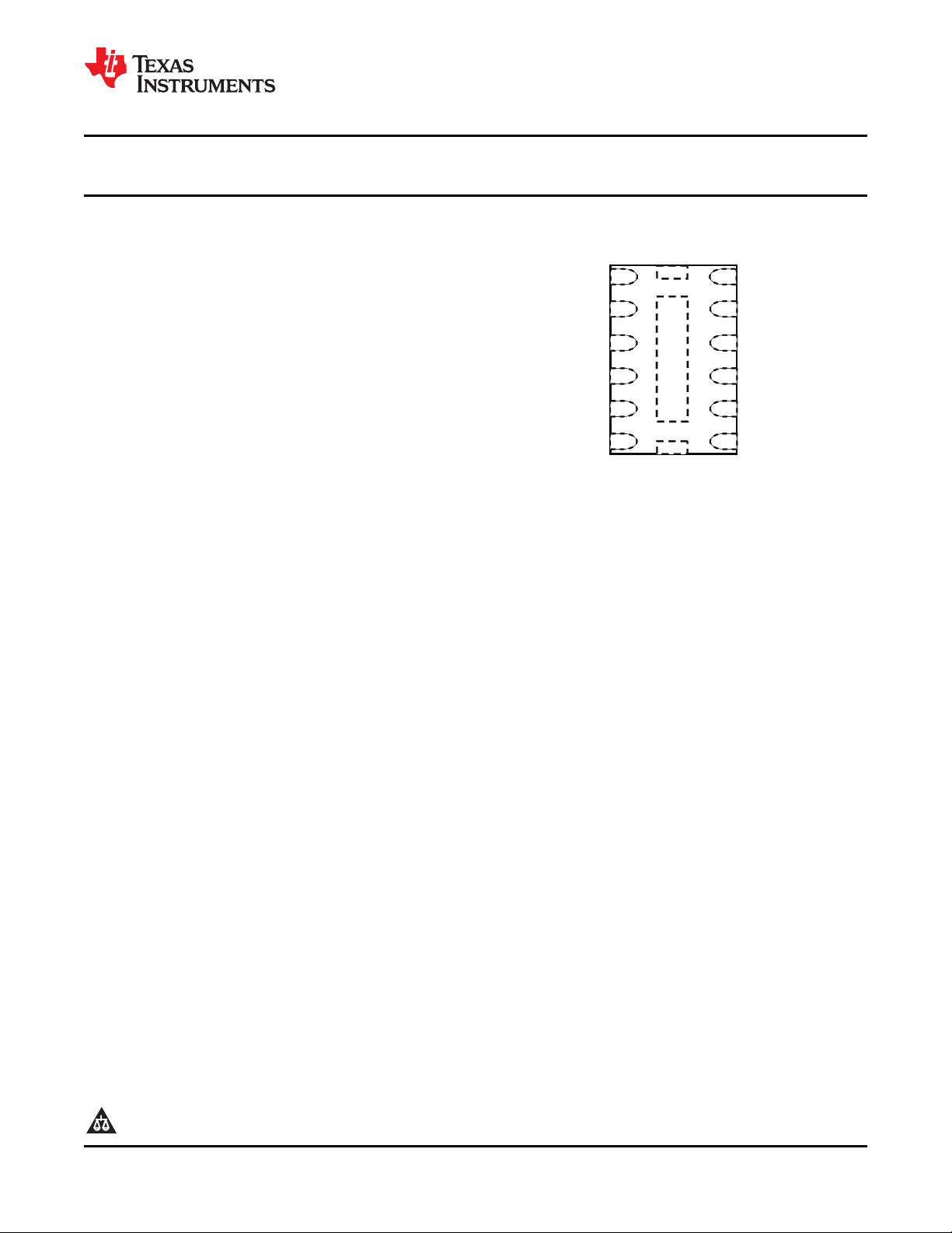
• Space-Saving SON Package (3 mm × 1.35 mm)
and Flow-Through Pin Mapping Provides
Optimum Filter Performance
TOTAL
= 34 pF)
SLLS876A –AUGUST 2008–REVISED NOVEMBER 2009
DSV PACKAGE
(TOP VIEW)
APPLICATIONS
• LCD Display Interface
• Keypad
• SVGA Video Connections
• Memory Interface
DESCRIPTION/ORDERING INFORMATION
The TPD6F002 is a six-channel EMI filter in a space-saving DSV package. This low-pass filter array reduces EMI
emissions and provides system-level ESD protection at the data ports. Because of its small package and
easy-to-use pin assignments, this device is suitable for a wide array of applications such as mobile handsets,
PDAs, video consoles, notebook computers, etc. In particular, the TPD6F002 is ideal for EMI filtering and
protecting data lines from ESD at the LCD display, keypad, and memory interfaces. The pi-style (C-R-C) filter
provides at least 35 dB attenuation in the carrier frequency range.
The TPD6F002 is a highly integrated device designed to suppress EMI/RFI noise in all systems subjected to
electromagnetic interferences. This filter includes ESD protection circuitry that prevents damage to the
application when subjected to ESD up to IEC 61000-4-2 ±20 kV Contact ESD and ±30 kV Air-Gap ESD.
The TPD6F002 is specified for –40°C to 85°C operation.
1
Please be aware that an important notice concerning availability, standard warranty, and use in critical applications of Texas
Instruments semiconductor products and disclaimers thereto appears at the end of this data sheet.
PRODUCTION DATA information is current as of publication date.
Products conform to specifications per the terms of the Texas
Instruments standard warranty. Production processing does not
necessarily include testing of all parameters.
Copyright © 2008–2009, Texas Instruments Incorporated
Page 2
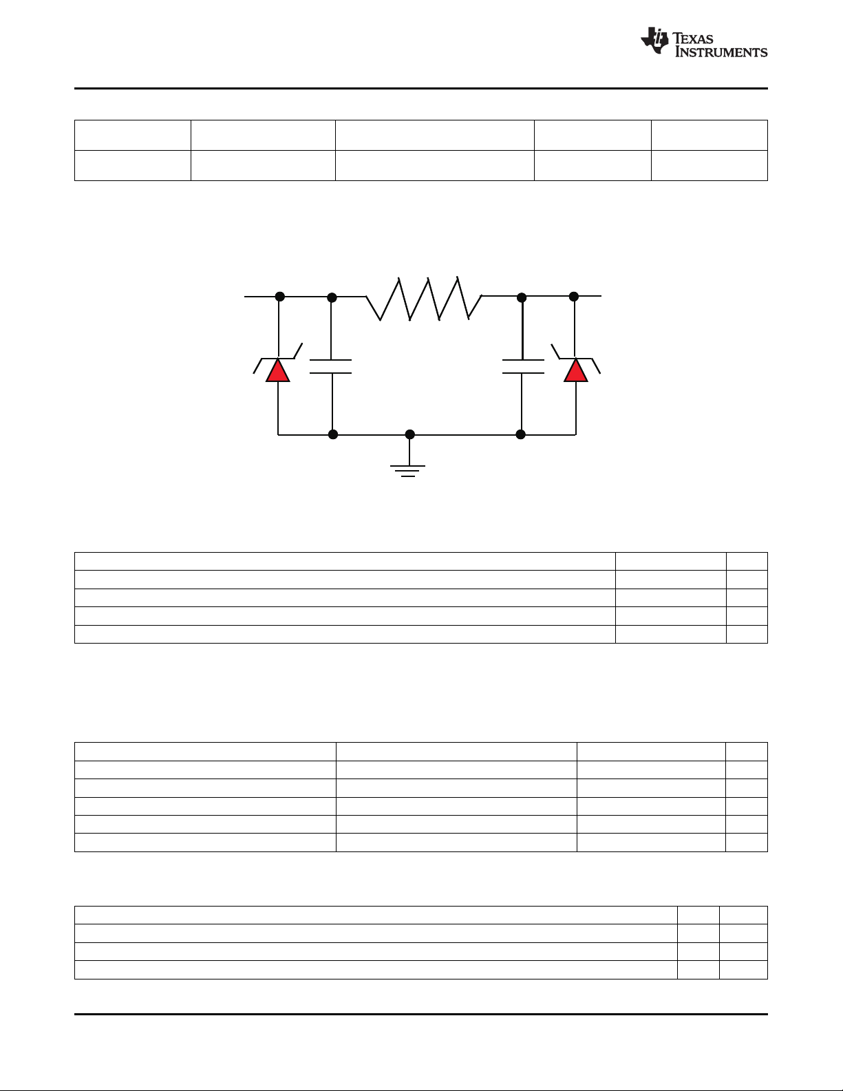
100Ω
C2=17pF
C1 =17pF
Ch_In
Ch_Out
GND
TPD6F002
SLLS876A –AUGUST 2008–REVISED NOVEMBER 2009
www.ti.com
ORDERING INFORMATION
T
A
–40°C to 85°C 0.5-mm pitch SON – DSV TPD6F002DSVR YM3NS
(1) For the most current package and ordering information, see the Package Option Addendum at the end of this document, or see the TI
web site at www.ti.com.
(2) Package drawings, thermal data, and symbolization are available at www.ti.com/packaging.
PACKAGE
(1) (2)
PACKAGE DIMENSION TOP-SIDE MARKING
Length = 3 mm, Width = 1.35 mm,
Pitch = 0.5 mm, Height = 0.75 mm)
ORDERABLE
PART NUMBER
EQUIVALENT SCHEMATIC REPRESENTATION
ABSOLUTE MAXIMUM RATINGS
(1)
over operating free-air temperature range (unless otherwise noted)
MIN MAX UNIT
V
T
T
(1) Stresses beyond those listed under "absolute maximum ratings" may cause permanent damage to the device. These are stress ratings
IO to GND 6 V
IO
Storage temperature range –65 150 °C
stg
Junction temperature 150 °C
J
Lead temperature (soldering, 10 s) 300 °C
only, and functional operation of the device at these or any other conditions beyond those indicated in the operational sections of the
specifications is not implied. Exposure to absolute maximum rated conditions for extended periods may affect device reliability.
ELECTRICAL CHARACTERISTICS
TA= –40°C to 85°C (Unless otherwise noted)
PARAMETER TEST CONDITIONS MIN TYP
V
R Resistance 85 100 115 Ω
C Capacitance (C1 or C2) VIO= 2.5 V 17 pF
I
f
(1) Typical values are at TA= 25°C.
DC breakdown voltage IIO= 10 μA 6 V
BR
Channel leakage current VIO= 3.3 V 1 20 nA
IO
Cut-off frequency Z
C
SOURCE
= 50 Ω, Z
= 50 Ω 100 MHz
LOAD
ESD PROTECTION
HBM ±15 kV
IEC 61000-4-2 Contact Discharge ±20 kV
IEC 61000-4-2 Air-Gap Discharge ±30 kV
PARAMETER TYP UNIT
(1)
MAX UNIT
2 Submit Documentation Feedback Copyright © 2008–2009, Texas Instruments Incorporated
Product Folder Link(s): TPD6F002
Page 3
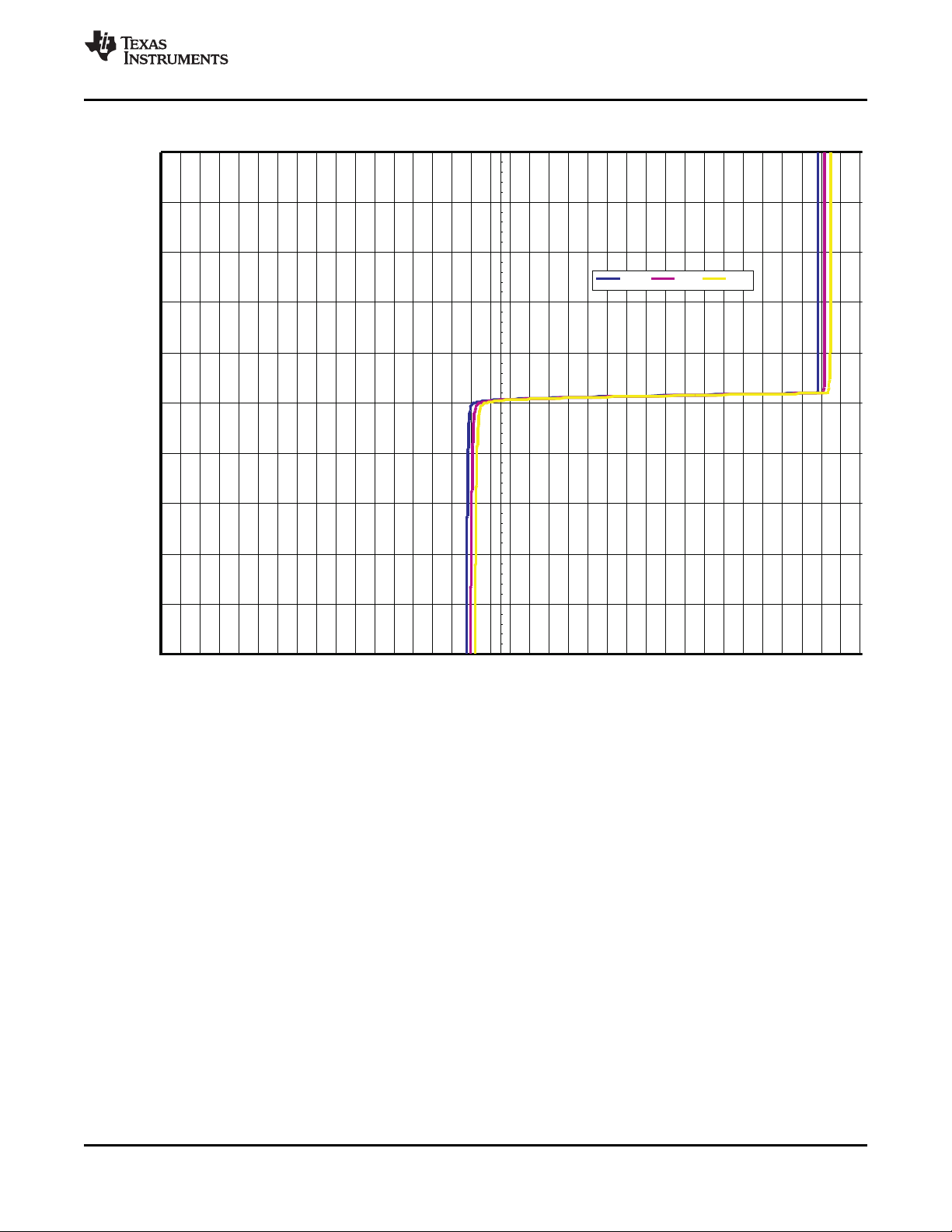
-1.0 0E-05
-8.0 0E-06
-6.0 0E-06
-4.0 0E-06
-2.0 0E-06
0.00E +00
2.00E-06
4.00E-06
6.00E-06
8.00E-06
1.00E-05
-7 -5 -3 -1 1 3 5 7
Volt age (V)
C u r re n t (µ A )
-40C 25C 85C
TPD6F002
www.ti.com
SLLS876A –AUGUST 2008–REVISED NOVEMBER 2009
TYPICAL OPERATING CHARACTERISTCS
Figure 1. DC Voltage-Current Sweep across Input, Output Pins
Copyright © 2008–2009, Texas Instruments Incorporated Submit Documentation Feedback 3
Product Folder Link(s): TPD6F002
Page 4
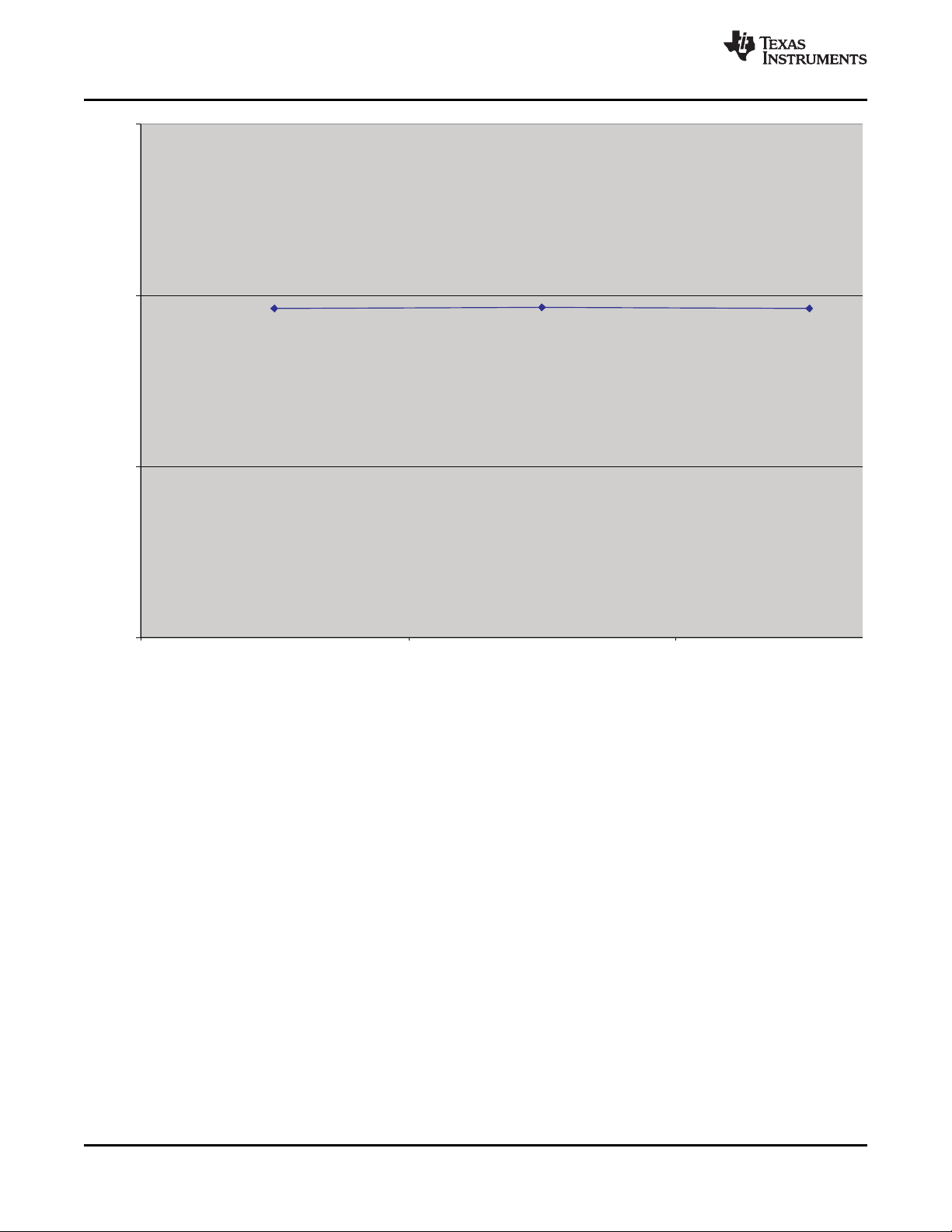
0
50
100
150
-40 25 85
Temp (C)
R e s i s ta n c e ( o h m s )
TPD6F002
SLLS876A –AUGUST 2008–REVISED NOVEMBER 2009
www.ti.com
Figure 2. Series Resistance vs Temperature
4 Submit Documentation Feedback Copyright © 2008–2009, Texas Instruments Incorporated
Product Folder Link(s): TPD6F002
Page 5
-100
-90
-80
-70
-60
-50
-40
-30
-20
-10
0
1.00E+06 1.00E+07 1.00E+08 1.00E+09
frequency (Hz)
S 4 1 ( d B )
TPD6F002
www.ti.com
SLLS876A –AUGUST 2008–REVISED NOVEMBER 2009
Figure 3. Channel-to-Channel Crosstalk
Copyright © 2008–2009, Texas Instruments Incorporated Submit Documentation Feedback 5
Product Folder Link(s): TPD6F002
Page 6

-45
-40
-35
-30
-25
-20
-15
-10
-5
0
1.00E+06 1.00E+07 1.00E+08 1.00E+09
Frequency (Hz)
I n s e rtio n L o s s ( d B )
TPD6F002
SLLS876A –AUGUST 2008–REVISED NOVEMBER 2009
www.ti.com
Figure 4. TPD6F002 Typical Insertion-loss Characteristics
(TA= 25°C, DC Bias = 0 V, 50 Ω Environment)
6 Submit Documentation Feedback Copyright © 2008–2009, Texas Instruments Incorporated
Product Folder Link(s): TPD6F002
Page 7

0
5
10
15
20
25
30
0 0.5 1 1.5 2 2.5 3 3.5 4 4.5
Voltage Bias (V)
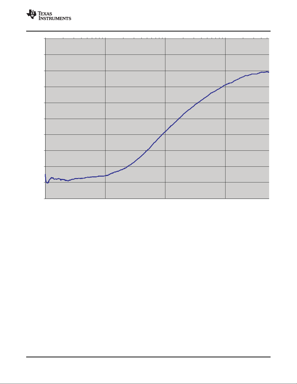
C a p ac i ta n c e (p F )
C1 C2
TPD6F002
www.ti.com
SLLS876A –AUGUST 2008–REVISED NOVEMBER 2009
Figure 5. Capacitance (C1 or C2) vs. Bias Voltage
Copyright © 2008–2009, Texas Instruments Incorporated Submit Documentation Feedback 7
Product Folder Link(s): TPD6F002
Page 8

PACKAGE OPTION ADDENDUM
www.ti.com 12-Mar-2010
PACKAGING INFORMATION
Orderable Device Status
(1)
Package
Type
Package
Drawing
Pins Package
Qty
Eco Plan
TPD6F002DSVR ACTIVE SON DSV 12 3000 Green (RoHS &
(2)
Lead/Ball Finish MSL Peak Temp
CU NIPDAU Level-1-260C-UNLIM
(3)
no Sb/Br)
(1)
The marketing status values are defined as follows:
ACTIVE: Product device recommended for new designs.
LIFEBUY: TI has announced that the device will be discontinued, and a lifetime-buy period is in effect.
NRND: Not recommended for new designs. Device is in production to support existing customers, but TI does not recommend using this part in
a new design.
PREVIEW: Device has been announced but is not in production. Samples may or may not be available.
OBSOLETE: TI has discontinued the production of the device.
(2)
Eco Plan - The planned eco-friendly classification: Pb-Free (RoHS), Pb-Free (RoHS Exempt), or Green (RoHS & no Sb/Br) - please check
http://www.ti.com/productcontent for the latest availability information and additional product content details.
TBD: The Pb-Free/Green conversion plan has not been defined.
Pb-Free (RoHS): TI's terms "Lead-Free" or "Pb-Free" mean semiconductor products that are compatible with the current RoHS requirements
for all 6 substances, including the requirement that lead not exceed 0.1% by weight in homogeneous materials. Where designed to be soldered
at high temperatures, TI Pb-Free products are suitable for use in specified lead-free processes.
Pb-Free (RoHS Exempt): This component has a RoHS exemption for either 1) lead-based flip-chip solder bumps used between the die and
package, or 2) lead-based die adhesive used between the die and leadframe. The component is otherwise considered Pb-Free (RoHS
compatible) as defined above.
Green (RoHS & no Sb/Br): TI defines "Green" to mean Pb-Free (RoHS compatible), and free of Bromine (Br) and Antimony (Sb) based flame
retardants (Br or Sb do not exceed 0.1% by weight in homogeneous material)
(3)
MSL, Peak Temp. -- The Moisture Sensitivity Level rating according to the JEDEC industry standard classifications, and peak solder
temperature.
Important Information and Disclaimer:The information provided on this page represents TI's knowledge and belief as of the date that it is
provided. TI bases its knowledge and belief on information provided by third parties, and makes no representation or warranty as to the
accuracy of such information. Efforts are underway to better integrate information from third parties. TI has taken and continues to take
reasonable steps to provide representative and accurate information but may not have conducted destructive testing or chemical analysis on
incoming materials and chemicals. TI and TI suppliers consider certain information to be proprietary, and thus CAS numbers and other limited
information may not be available for release.
In no event shall TI's liability arising out of such information exceed the total purchase price of the TI part(s) at issue in this document sold by TI
to Customer on an annual basis.
Addendum-Page 1
Page 9

PACKAGE MATERIALS INFORMATION
www.ti.com 20-Jul-2010
TAPE AND REEL INFORMATION
*All dimensions are nominal
Device Package
TPD6F002DSVR SON DSV 12 3000 180.0 8.4 1.74 3.33 1.05 4.0 8.0 Q1
Type
Package
Drawing
Pins SPQ Reel
Diameter
(mm)
Reel
Width
W1 (mm)
A0
(mm)B0(mm)K0(mm)P1(mm)W(mm)
Pin1
Quadrant
Pack Materials-Page 1
Page 10

PACKAGE MATERIALS INFORMATION
www.ti.com 20-Jul-2010
*All dimensions are nominal
Device Package Type Package Drawing Pins SPQ Length (mm) Width (mm) Height (mm)
TPD6F002DSVR SON DSV 12 3000 202.0 201.0 28.0
Pack Materials-Page 2
Page 11

Page 12

Page 13

Page 14

IMPORTANT NOTICE
Texas Instruments Incorporated and its subsidiaries (TI) reserve the right to make corrections, modifications, enhancements, improvements,
and other changes to its products and services at any time and to discontinue any product or service without notice. Customers should
obtain the latest relevant information before placing orders and should verify that such information is current and complete. All products are
sold subject to TI’s terms and conditions of sale supplied at the time of order acknowledgment.
TI warrants performance of its hardware products to the specifications applicable at the time of sale in accordance with TI’s standard
warranty. Testing and other quality control techniques are used to the extent TI deems necessary to support this warranty. Except where
mandated by government requirements, testing of all parameters of each product is not necessarily performed.
TI assumes no liability for applications assistance or customer product design. Customers are responsible for their products and
applications using TI components. To minimize the risks associated with customer products and applications, customers should provide
adequate design and operating safeguards.
TI does not warrant or represent that any license, either express or implied, is granted under any TI patent right, copyright, mask work right,
or other TI intellectual property right relating to any combination, machine, or process in which TI products or services are used. Information
published by TI regarding third-party products or services does not constitute a license from TI to use such products or services or a
warranty or endorsement thereof. Use of such information may require a license from a third party under the patents or other intellectual
property of the third party, or a license from TI under the patents or other intellectual property of TI.
Reproduction of TI information in TI data books or data sheets is permissible only if reproduction is without alteration and is accompanied
by all associated warranties, conditions, limitations, and notices. Reproduction of this information with alteration is an unfair and deceptive
business practice. TI is not responsible or liable for such altered documentation. Information of third parties may be subject to additional
restrictions.
Resale of TI products or services with statements different from or beyond the parameters stated by TI for that product or service voids all
express and any implied warranties for the associated TI product or service and is an unfair and deceptive business practice. TI is not
responsible or liable for any such statements.
TI products are not authorized for use in safety-critical applications (such as life support) where a failure of the TI product would reasonably
be expected to cause severe personal injury or death, unless officers of the parties have executed an agreement specifically governing
such use. Buyers represent that they have all necessary expertise in the safety and regulatory ramifications of their applications, and
acknowledge and agree that they are solely responsible for all legal, regulatory and safety-related requirements concerning their products
and any use of TI products in such safety-critical applications, notwithstanding any applications-related information or support that may be
provided by TI. Further, Buyers must fully indemnify TI and its representatives against any damages arising out of the use of TI products in
such safety-critical applications.
TI products are neither designed nor intended for use in military/aerospace applications or environments unless the TI products are
specifically designated by TI as military-grade or "enhanced plastic." Only products designated by TI as military-grade meet military
specifications. Buyers acknowledge and agree that any such use of TI products which TI has not designated as military-grade is solely at
the Buyer's risk, and that they are solely responsible for compliance with all legal and regulatory requirements in connection with such use.
TI products are neither designed nor intended for use in automotive applications or environments unless the specific TI products are
designated by TI as compliant with ISO/TS 16949 requirements. Buyers acknowledge and agree that, if they use any non-designated
products in automotive applications, TI will not be responsible for any failure to meet such requirements.
Following are URLs where you can obtain information on other Texas Instruments products and application solutions:
Products Applications
Amplifiers amplifier.ti.com Audio www.ti.com/audio
Data Converters dataconverter.ti.com Automotive www.ti.com/automotive
DLP® Products www.dlp.com Communications and www.ti.com/communications
DSP dsp.ti.com Computers and www.ti.com/computers
Clocks and Timers www.ti.com/clocks Consumer Electronics www.ti.com/consumer-apps
Interface interface.ti.com Energy www.ti.com/energy
Logic logic.ti.com Industrial www.ti.com/industrial
Power Mgmt power.ti.com Medical www.ti.com/medical
Microcontrollers microcontroller.ti.com Security www.ti.com/security
RFID www.ti-rfid.com Space, Avionics & www.ti.com/space-avionics-defense
RF/IF and ZigBee® Solutions www.ti.com/lprf Video and Imaging www.ti.com/video
Mailing Address: Texas Instruments, Post Office Box 655303, Dallas, Texas 75265
Copyright © 2010, Texas Instruments Incorporated
Telecom
Peripherals
Defense
Wireless www.ti.com/wireless-apps
 Loading...