

Page 1
www.ti.com
Filter and
I/V Gain Stage
Stereo Hi−Fi
Headphone Driver
TPA6120A2
DYR > 120 dB
for Whole
System!
OUT A
OUT B
OUT C
OUT D
C
F
2.7 nF
R
F
LIN−
LIN+
R
F
RIN−
RIN+
R
I
1 kΩ
1 kΩ
LOUT
ROUT
1 kΩ
R
F
R
O
10 Ω
R
O
10 Ω
1 kΩ
R
F
R
F
1 kΩ
R
I
1 kΩ
R
I
1 kΩ
R
I
1 kΩ
C
F
2.7 nF
R
F
1 kΩ
1 kΩ
C
F
2.7 nF
R
F
C
F
2.7 nF
R
F
1 kΩ
1 kΩ
1/2 OPA4134
1/2 OPA4134
−IN A
−IN B
+IN B
+IN A
−IN C
−IN D
+IN D
+IN C
PCM
Audio
Data
Source
Controller
PCM1792
or
DSD1792
LRCK
BCK
DATA
RST
SCK
MDO
MC
MDI
MS
ZEROL
ZEROR
I
OUT
L−
I
OUT
L+
I
OUT
R−
I
OUT
R+
AUDIO DAC
HIGH FIDELITY HEADPHONE AMPLIFIER
FEATURES DESCRIPTION
• 80 mW into 600 Ω From a ±12-V Supply at
0.00014% THD + N
• Current-Feedback Architecture
• Greater than 120 dB of Dynamic Range
• SNR of 120 dB
• Output Voltage Noise of 5 µVrms at
Gain = 2 V/V
• Power Supply Range: ±5 V to ±15 V
• 1300 V/µs Slew Rate
• Differential Inputs
• Independent Power Supplies for Low
Crosstalk
• Short Circuit and Thermal Protection
APPLICATIONS
• Professional Audio Equipment
• Mixing Boards
• Headphone Distribution Amplifiers
• Headphone Drivers
• Microphone Preamplifiers
TPA6120A2
SLOS431 – MARCH 2004
The TPA6120A2 is a high fidelity audio amplifier built
on a current-feedback architecture. This high
bandwidth, extremely low noise device is ideal for
high performance equipment. The better than 120 dB
of dynamic range exceeds the capabilities of the
human ear, ensuring that nothing audible is lost due
to the amplifier. The solid design and performance of
the TPA6120A2 ensures that music, not the amplifier,
is heard.
Three key features make current-feedback amplifiers
outstanding for audio. The first feature is the high
slew rate that prevents odd order distortion
anomalies. The second feature is current-on-demand
at the output that enables the amplifier to respond
quickly and linearly when necessary without risk of
output distortion. When large amounts of output
power are suddenly needed, the amplifier can respond extremely quickly without raising the noise
floor of the system and degrading the signal-to-noise
ratio. The third feature is the gain-independent frequency response that allows the full bandwidth of the
amplifier to be used over a wide range of gain
settings. The excess loop gain does not deteriorate at
a rate of 20 dB/decade.
PowerPAD is a trademark of Texas Instruments.
PRODUCTION DATA information is current as of publication date.
Products conform to specifications per the terms of the Texas
Instruments standard warranty. Production processing does not
necessarily include testing of all parameters.
Please be aware that an important notice concerning availability, standard warranty, and use in critical applications of Texas
Instruments semiconductor products and disclaimers thereto appears at the end of this data sheet.
Copyright © 2004, Texas Instruments Incorporated
Page 2
www.ti.com
TPA6120A2
SLOS431 – MARCH 2004
These devices have limited built-in ESD protection. The leads should be shorted together or the device placed in conductive foam
during storage or handling to prevent electrostatic damage.
ABSOLUTE MAXIMUM RATINGS
over operating free-air temperature range (unless otherwise noted)
Supply voltage, V
Input voltage, V
Differential input voltage, V
Minimum load impedance 8 Ω
Continuous total power dissipation See Dissipation Rating Table
Operating free–air temperature range, T
Operating junction temperature range, T
Storage temperature range, T
Lead temperature 1,6 mm (1/16 inch) from case for 10 seconds 235°C
(1) Stresses beyond those listed under “absolute maximum ratings” may cause permanent damage to the device. These are stress ratings
only, and functional operation of the device at these or any other conditions beyond those indicated under “recommended operating
conditions” is not implied. Exposure to absolute–maximum–rated conditions for extended periods may affect device reliability.
(2) When the TPA6120A2 is powered down, the input source voltage must be kept below 600-mV peak.
(3) The TPA6120A2 incorporates an exposed PowerPAD on the underside of the chip. This acts as a heatsink and must be connected to a
thermally dissipating plane for proper power dissipation. Failure to do so may result in exceeding the maximum junction temperature that
could permanently damage the device. See TI Technical Brief SLMA002 for more information about utilizing the PowerPAD thermally
enhanced package.
to V
CC+
(2)
I
CC-
ID
A
(3)
J
stg
(1)
TPA6120A2
33 V
± V
CC
6 V
- 40°C to 85°C
- 40°C to 150°C
- 40°C to 125°C
DISSIPATION RATING TABLE
(1)
θ
PACKAGE
JA
(°C/W) (°C/W) POWER RATING
DWP 44.4 33.8 2.8 W
θ
JC
TA= 25°C
(1) The PowerPAD must be soldered to a thermal land on the printed-circuit board. See the PowerPAD
Thermally Enhanced Package application note (SLMA002)
AVAILABLE OPTIONS
T
A
-40°C to 85°C DWP
(1) The DWP package is available taped and reeled. To order a taped and reeled part, add the suffix R
to the part number (e.g., TPA6120A2DWPR).
PACKAGE PART NUMBER SYMBOL
(1)
RECOMMENDED OPERATING CONDITIONS
Supply voltage, V
Load impedance V
Operating free–air temperature, T
and V
CC+
CC-
A
TPA6120A2DWP 6120A2
MIN MAX UNIT
Split Supply ±5 ±15
Single Supply 10 30
= ±5 V or ±15 V 16 Ω
CC
-40 85 °C
V
2
Page 3
www.ti.com
ELECTRICAL CHARACTERISTICS
over operating free-air temperature range (unless otherwise noted)
PARAMETER TEST CONDITIONS MIN TYP MAX UNIT
|V
| Input offset voltage (measured differentially) V
IO
PSRR Power supply rejection ratio V
V
IC
I
CC
I
O
r
i
r
o
V
O
Common mode input voltage V
Supply current (each channel) mA
Output current (per channel) VCC= ±5 V to ±15 V 700 mA
Input offset voltage drift V
Input resistance 300 kΩ
Output resistance Open Loop 13 Ω
Output voltage swing V
TPA6120A2
SLOS431 – MARCH 2004
= ±5 V or ±15 V 2 5 mV
CC
= 2.5 V to 5.5 V 75 dB
CC
V
= ±5 V ±3.6 ±3.7
CC
V
= ±15 V ±13.4 ±13.5
CC
V
= ±5 V 11.5 13
CC
VCC= ±15 V 15
= ±5 V or ±15 V 20 µV/°C
CC
= ±15 V, RL= 25 Ω V
CC
11.8 to 12.5 to
-11.5 -12.2
3
Page 4
www.ti.com
TPA6120A2
SLOS431 – MARCH 2004
OPERATING CHARACTERISTICS
TA= 25°C, RL= 25 Ω, Gain = 2 V/V (unless otherwise noted)
PARAMETER TEST CONDITIONS MIN TYP MAX UNIT
IMD
THD+N
k
SVR
CMRR V
SR Slew rate V/µs
V
n
SNR Signal-to-noise ratio RL= 32 Ω to 64 Ω dB
(1) For IMD, THD+N, k
Intermodulation distortion Gain = 2 V/V,
(SMPTE) IM frequency = 60 Hz
Total harmonic distortion
plus noise
Supply voltage rejection
ratio
Common mode rejection
ratio (differential)
Output noise voltage RL= 32 Ω to 64 Ω µVrms
Dynamic range dB
Crosstalk RL= 32 Ω to 64 Ω -90 dB
, and crosstalk, the bandwidth of the measurement instruments was set to 80 kHz.
SVR
(1)
V
= ±12 V to ±15 V,
CC
SMTPE ratio = 4:1,
High frequency = 7 kHz
PO= 100 mW, RL= 32 Ω
f = 1 kHz
PO= 100 mW, RL= 64 Ω
f = 1 kHz
V
= ±12 V, Gain = 3 V/V
CC
RL= 600 Ω, f = 1 kHz
V
= ±15 V, Gain = 3 V/V
CC
RL= 600 Ω, f = 1 kHz
V
= ±12 V,
CC
Gain = 3 V/V
V
= ±15 V,
CC
Gain = 3 V/V
RL= 32 Ω, 0.00014%
VI= 1 V
PP
V
= ±12 V to ±15 V,
CC
RL= 64 Ω, 0.000095%
VI= 1 V
PP
V
= ±12 V 0.00055%
CC
V
= ±15 V 0.00060%
CC
V
= ±12 V 0.00038%
CC
V
= ±15 V 0.00029%
CC
PO= 80 mW 0.00014%
PO= 40 mW 0.000065%
PO= 125 mW 0.00012%
PO= 62.5 mW 0.000061%
VO= 15 VPP,
RL= 10 kΩ 0.000024%
f = 1 kHz
VO= 15 VPP,
RL= 10 kΩ 0.000021%
f = 1 kHz
RL= 32 Ω VCC= ±12 V -80
f = 10 Hz to 22 kHz
V
= 1 V
(RIPPLE)
PP
VCC= ±15 V -83
RL= 64 Ω VCC= ±12 V -76
f = 10 Hz to 22 kHz
V
V
V
V
= 1 V
(RIPPLE)
= ±5 V or ±15 V 100 dB
CC
= ±15 V, Gain = 5 V/V, VO= 20 V
CC
= ±5 V, Gain = 2 V/V, VO= 5 V
CC
= ±12 V to ±15 V Gain = 2 V/V 5
CC
PP
f = 1 kHz
V
= ±12 V to ±15 V Gain = 2 V/V 125
CC
f = 1 kHz
RL= 32 Ω, f = 1 kHz
RL= 64 Ω, f = 1 kHz
V
= ±12 V to ±15 V
CC
f = 1 kHz
VCC= ±15 V -79
PP
PP
Gain = 100 V/V 50
Gain = 100 V/V 104
V
= ±12 V 123
CC
V
= ±15 V 125
CC
V
= ±12 V 124
CC
V
= ±15 V 126
CC
VI= 1 V
RMS
RF= 1 kΩ
1300
900
dB
4
Page 5
www.ti.com
DEVICE INFORMATION
1
2
3
4
5
6
7
8
9
10
20
19
18
17
16
15
14
13
12
11
LVCC−
LOUT
LVCC+
LIN+
LIN−
NC
NC
NC
NC
NC
RVCC−
ROUT
RVCC+
RIN+
RIN−
NC
NC
NC
NC
NC
NC − No internal connection
Thermally Enhansed SOIC (DWP)
PowerPAD™ Package
Top View
TERMINAL FUNCTIONS
PIN NAME PIN NUMBER I/O DESCRIPTION
LVCC- 1 I
LOUT 2 O Left channel output
LVCC+ 3 I Left channel positive power supply
LIN+ 4 I Left channel positive input
LIN- 5 I Left channel negative input
NC 6,7,8,9,10,11,12,13,14,15 - Not internally connected
RIN- 16 I Right channel negative input
RIN+ 17 I Right channel positive input
RVCC+ 18 I Right channel positive power supply
ROUT 19 O Right channel output
RVCC- 20 I
Thermal Pad - -
Left channel negative power supply – must be kept at the same potential as
RVCC-.
Right channel negative power supply - must be kept at the same potential as
LVCC-.
Connect to ground. The thermal pad must be soldered down in all
applications to properly secure device on the PCB.
TPA6120A2
SLOS431 – MARCH 2004
5
Page 6

www.ti.com
0.001
0.01
10 100 1 k 10 k 50 k
THD+N −Total Harmonic Distortion + Noise − %
f − Frequency − Hz
RL = 10 k,
Gain = 3 V/V ,
RF = 2 k,
RI = 1 k,
BW = 80 kHz
VCC = 15 VO = 15 V
PP
VCC = 12 VO = 15 V
PP
VCC = 12 VO = 12 V
PP
VCC = 15 VO = 23 V
PP
0.0001
0.00001
0.0001
0.001
0.01
10 100 1 k 10 k 50 k
RL = 600 ,
Gain = 3 V/V ,
RF = 2 k,
RI = 1 k,
BW = 80 kHz
THD+N −Total Harmonic Distortion + Noise − %
f − Frequency − Hz
VCC = 12 V ,
PO = 80 mW
VCC = 15 V ,
PO = 125 mW
TPA6120A2
SLOS431 – MARCH 2004
TYPICAL CHARACTERISTICS
Table of Graphs
vs Frequency 1, 2, 3, 4
Total harmonic distortion + noise vs Output voltage 5
vs Output power 6, 7, 8
Power dissipation vs Output power 9
Supply voltage rejection ratio vs Frequency 10, 11
Intermodulation distortion
Crosstalk vs Frequency 14
Signal-to-noise ratio vs Gain 15, 16
Slew rate vs Output step 17, 18
Small and large signal frequency response 19, 20
400-mV step response 21
10-V step response 22
20-V step response 23
vs High frequency 12
vs IM Amplitude 13
FIGURE
TOTAL HARMONIC DISTORTION + NOISE TOTAL HARMONIC DISTORTION + NOISE
vs vs
FREQUENCY FREQUENCY
Figure 1. Figure 2.
6
Page 7
www.ti.com
0.0001
0.01
0.1
1 k 10 k 50 k
THD+N −Total Harmonic Distortion + Noise − %
f − Frequency − Hz
RL = 64 ,
Gain = 2 V/V ,
RF = 1 k,
RI = 1 k,
BW = 80 kHz
VCC = 15 V , PO = 700 mW
VCC = 15 V , PO = 1.35 W
10
100
VCC = 12 V , PO = 500 mW
VCC = 12 V , PO = 425 mW
0.001
THD+N −Total Harmonic Distortion + Noise − %
f − Frequency − Hz
0.001
1
10 100 1 k 10 k 50 k
0.01
0.1
RL = 32 ,
Gain = 2 V/V ,
RF = 1 k,
RI = 1 k,
BW = 80 kHz
0.0001
VCC = 15 V , PO = 1.5 W
VCC = 12 V , PO = 800 mW
VCC = 12 V , PO = 950 mW
VCC = 15 V , PO = 1.25 W
0.001
0.01
0.1
1
10
3 5 10 15 20 25 30 35
THD+N −Total Harmonic Distortion + Noise − %
VO − Output Voltage − V
PP
RL = 10 k,
Gain = 3 V/V ,
f = 1 kHz,
RF = 2 k,
RI = 1 k,
BW = 80 kHz
VCC = 12 V
VCC = 15 V
0.0001
0.00001
THD+N −Total Harmonic Distortion + Noise − %
PO − Output Power − W
0.00001
0.01
1
10
0.01 0.1 0.2
0.0001
0.001
0.1
VCC = 15 V
VCC = 12 V
RL = 600 ,
Gain = 3 V/V ,
f = 1 kHz,
RF = 2 k,
RI = 1 k,
BW = 80 kHz
TYPICAL CHARACTERISTICS (continued)
TPA6120A2
SLOS431 – MARCH 2004
TOTAL HARMONIC DISTORTION + NOISE TOTAL HARMONIC DISTORTION + NOISE
vs vs
FREQUENCY FREQUENCY
Figure 3. Figure 4.
TOTAL HARMONIC DISTORTION + NOISE TOTAL HARMONIC DISTORTION + NOISE
vs vs
OUTPUT VOLTAGE OUTPUT POWER
Figure 5. Figure 6.
7
Page 8
www.ti.com
THD+N −Total Harmonic Distortion + Noise − %
0.01
1
10
0.01 0.1 2
0.0001
0.001
0.1
PO − Output Power − W
VCC = 15 V
VCC = 12 V
1
RL = 64 ,
Gain = 2 V/V ,
f = 1 kHz,
RF = 1 k,
RI = 1 k,
BW = 80 kHz
THD+N −Total Harmonic Distortion + Noise − %
0.01
1
10
0.01 3
0.0001
0.001
0.1
PO − Output Power − W
VCC = 15 V
VCC = 12 V
0.1 1 2 4
RL = 32 ,
Gain = 2 V/V ,
f = 1 kHz,
RF = 1 k,
RI = 1 k,
BW = 80 kHz
−90
−80
−70
−60
−50
−40
−30
−20
0
10 100 1 k 10 k 50 k
32
k
SVR
− Supply Voltage Rejection Ratio − dB
f − Frequency − Hz
64
−10
VCC = 12 V ,
V
(ripple)
= 1 VPP,
Gain = 2 V/V
BW = 80 kHz
Representative of both positive and
negative supplies.
− Power Dissipation − W
P
D
0
0.2
0.4
0.6
0.8
1
1.2
1.4
1.6
1.8
2
0 0.5 1 1.5 2 2.5 3 3.5
VCC = 15 V , RL = 32
VCC = 15 V ,
RL = 64
VCC = 12 V ,
RL = 64
VCC = 12 V , RL = 32
PO − Output Power − W
Mono Operation
TPA6120A2
SLOS431 – MARCH 2004
TYPICAL CHARACTERISTICS (continued)
TOTAL HARMONIC DISTORTION + NOISE TOTAL HARMONIC DISTORTION + NOISE
vs vs
OUTPUT POWER OUTPUT POWER
Figure 7. Figure 8.
POWER DISSIPATION SUPPLY VOLTAGE REJECTION RATIO
vs vs
OUTPUT POWER FREQUENCY
8
Figure 9. Figure 10.
Page 9

www.ti.com
0.0001
0.001
0.01
0.1
2 k 10 k 50 k
Intermodulation Distortion − %
f − High Frequency − Hz
4:1 SMPTE Ratio
VI = 1 VPP,
Gain = 2 V/V ,
IM Frequency = 60 Hz
VCC = 12 V ,
RL = 32
VCC = 12 V ,
RL = 64
VCC = 15 V ,
RL = 64
0.00001
VCC = 15 V ,
RL = 32
−90
−80
−70
−60
−50
−40
−30
−20
−0
10 100 1 k 10 k 50 k
32
k
SVR
− Supply Voltage Rejection Ratio − dB
f − Frequency − Hz
−10
VCC = 15 V ,
V
(ripple)
= 1 VPP,
Gain = 2 V/V
BW = 80 kHz
64
Representative of both positive and
negative supplies.
−120
−110
−100
−90
−80
−70
−60
10
100
1 k 10 k 50 k
RF = 1 k,
Gain = 2 V/V ,
BW = 80 kHz
Crosstalk − dB
f − Frequency − Hz
VCC = 12 V ,
RL = 32
VCC = 15 V ,
RL = 64
VCC = 12 V ,
RL = 64
VCC = 15 V ,
RL = 32
IM Amplitude (At Input) − V
PP
0.00001
0.01
1
10
0 1 10
0.0001
0.001
0.1
VCC = 15 V , RL = 32
VCC = 12 V , RL = 64
VCC = 12 V , RL = 32
4:1 SMPTE Ratio
Gain = 3 V/V ,
High Frequency = 7 kHz
IM Frequency = 60 Hz
2 3 4 5 6 7 8 9
VCC = 15 V , RL = 64
Intermodulation Distortion − %
TYPICAL CHARACTERISTICS (continued)
TPA6120A2
SLOS431 – MARCH 2004
SUPPLY VOLTAGE REJECTION RATIO INTERMODULATION DISTORTION
vs vs
FREQUENCY HIGH FREQUENCY
Figure 11. Figure 12.
INTERMODULATION DISTORTION CROSSTALK
vs vs
IM AMPLITUDE (AT INPUT) FREQUENCY
Figure 13. Figure 14.
9
Page 10
www.ti.com
Signal−To−Noise Ratio − dB
100
120
110
130
1 10 20 30 40 50 60 70
Gain − V/V
80 90 100
VCC = 12 V
RI = 64
RI = 32
105
115
125
Signal−To−Noise Ratio − dB
100
105
110
115
120
125
130
1 10 20 30 40 50 60 70
Gain − V/V
80 90 100
VCC = 15 V
THD+N, RI = 64
THD+N, RI = 32
0
Output Step (Peak−To−Peak) − V
1500
100
20
900
5
1100
700
10
1300
500
300
VCC = ± 15 V
Gain = 5 V/V
RF = 1 kΩ
RL = 25 Ω
15
+SR
−SR
Slew Rate − V/
sµ
0
Output Step (Peak−To−Peak) − V
1000
100
5
700
1
800
600
2 3
900
Slew Rate − V/
sµ
500
300
4
VCC = ± 5 V
Gain = 2 V/V
RF = 1 kΩ
RL = 25 Ω
400
200
+SR
−SR
TPA6120A2
SLOS431 – MARCH 2004
TYPICAL CHARACTERISTICS (continued)
SIGNAL-TO-NOISE RATIO SIGNAL-TO-NOISE RATIO
vs vs
GAIN GAIN
Figure 15. Figure 16.
SLEW RATE SLEW RATE
vs vs
OUTPUT STEP OUTPUT STEP
10
Figure 17. Figure 18.
Page 11
www.ti.com
10M100k 500M1M 100M10k1k10010
f − Frequency − Hz
−27
−30
−18
−15
Output Level − dBV
−12
−3
−9
−6
VI = 500 mV
−24
−21
Gain = 1 V/V
VCC = ± 15 V
RF = 820 Ω
RL = 25 Ω
VI = 250 mV
VI = 125 mV
VI = 62.5 mV
10M100k 500M1M 100M10k1k10010
f − Frequency − Hz
−21
−24
−12
−9
Output Level − dBV
−6
3
−3
0
VI = 500 mV
−18
−15
Gain = 2 V/V
VCC = ± 15 V
RF = 680 Ω
RL = 25 Ω
VI = 250 mV
VI = 125 mV
VI = 62.5 mV
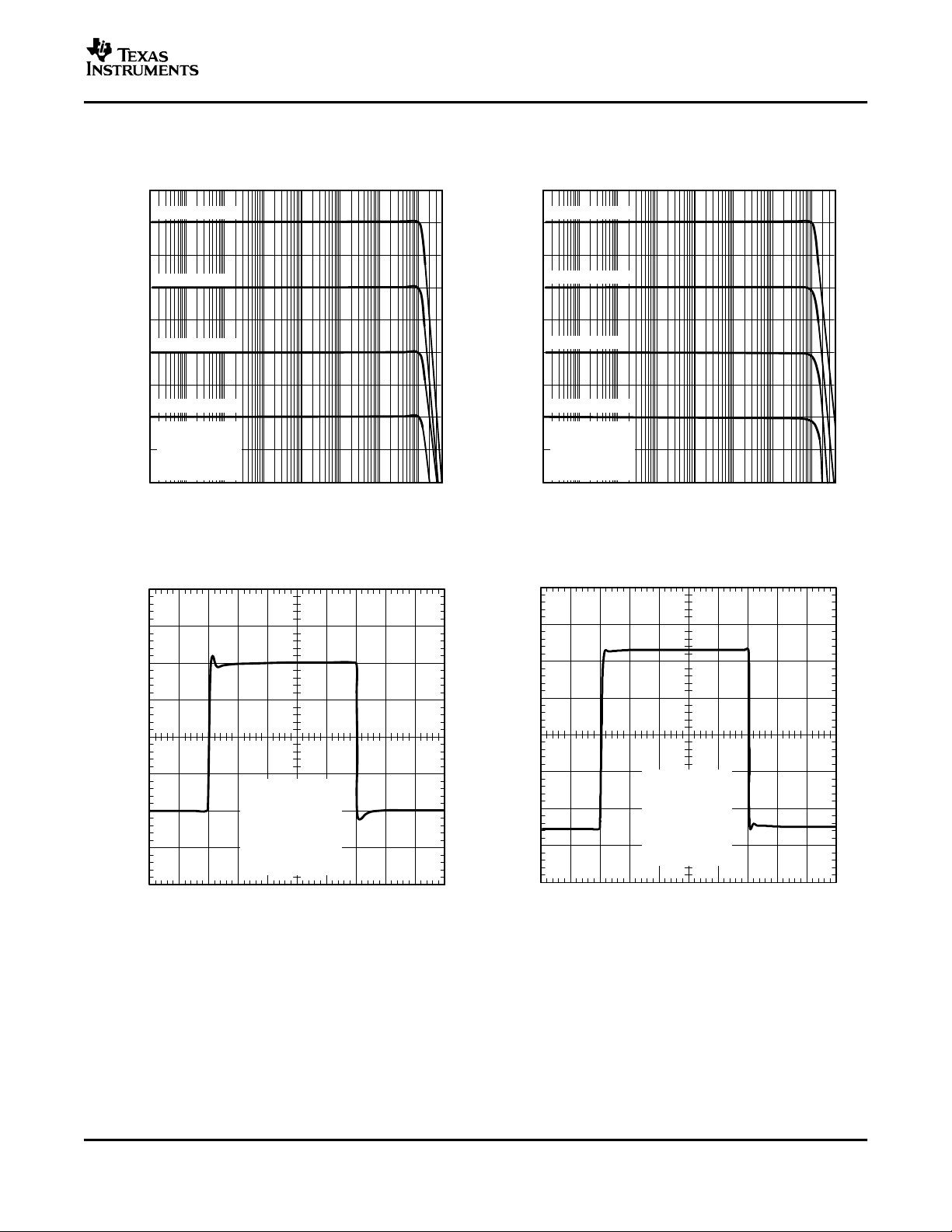
t − Time − ns
VCC = ±15 V
Gain = 2 V/V
RL = 25 Ω
RF = 1 kΩ
tr/tf= 300 ps
See Figure 3
100
−100
0
−200
V
O
− Output Voltage − mV
300
200
0 15010050 200 250 350300 400 450 500
400
−300
−400
t − Time − ns
2
−2
0
−4
V
O
− Output Voltage − V
6
4
0 15010050 200 250 350300 400 450 500
8
−6
−8
VCC = ±15 V
Gain = 2 V/V
RL = 25 Ω
RF = 1 kΩ
tr/tf= 5 ns
See Figure 3
TYPICAL CHARACTERISTICS (continued)
SMALL AND LARGE SIGNAL SMALL AND LARGE SIGNAL
FREQUENCY RESPONSE FREQUENCY RESPONSE
TPA6120A2
SLOS431 – MARCH 2004
400-mV STEP RESPONSE 10-V STEP RESPONSE
Figure 19. Figure 20.
Figure 21. Figure 22.
11
Page 12
www.ti.com
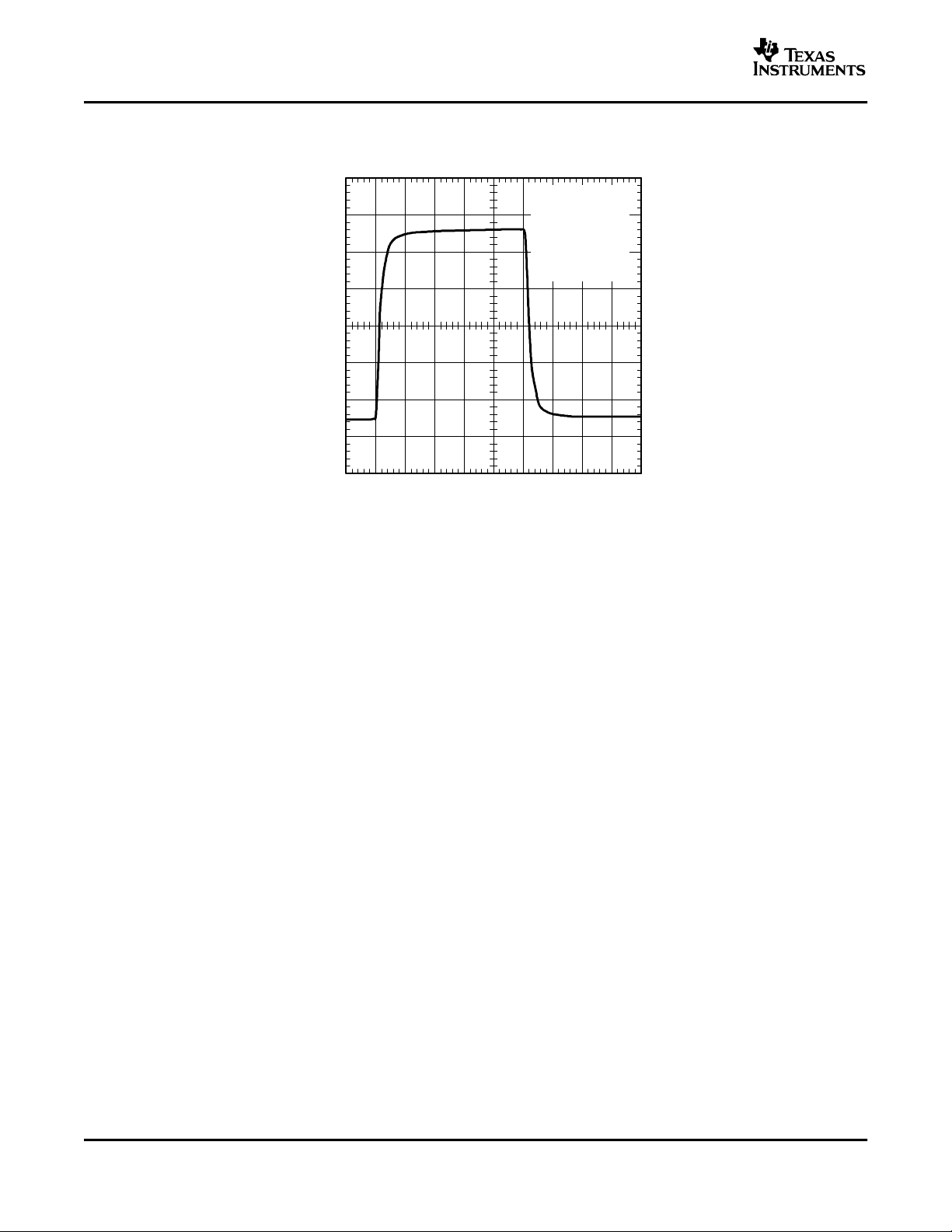
t − Time − ns
VCC = ±15 V
Gain = 5 V/V
RL = 25 Ω
RF = 2 kΩ
tr/tf= 5 ns
See Figure 3
4
−4
0
−8
V
O
− Output Voltage − V
12
8
0 15010050 200 250 350300 400 450 500
16
−12
−16
TPA6120A2
SLOS431 – MARCH 2004
TYPICAL CHARACTERISTICS (continued)
20-V STEP RESPONSE
Figure 23.
12
Page 13
www.ti.com
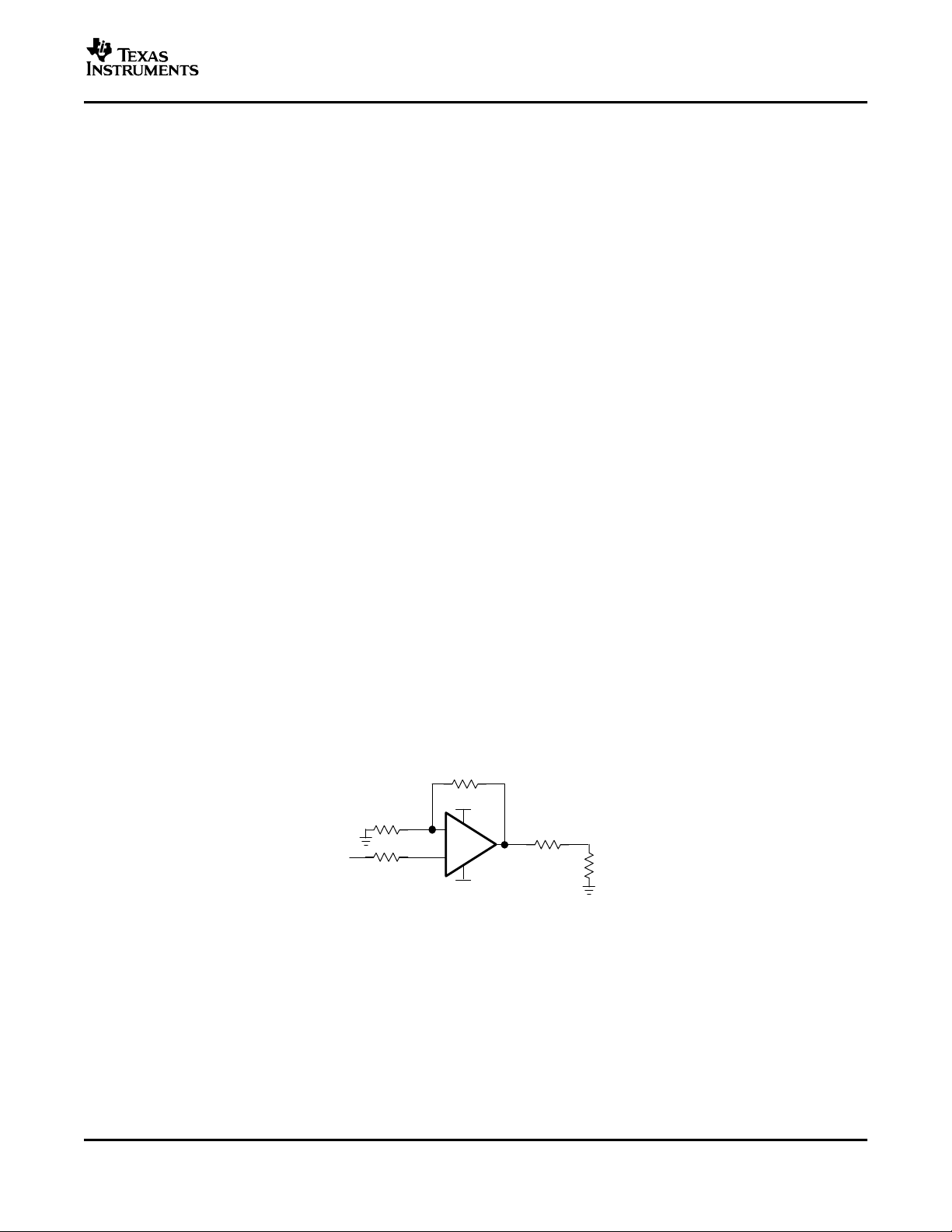
−
+
R
F
= 1 k
V
CC+
R
I
= 1 k
R
S
= 50
R
O
= 10
R
L
V
I
V
CC−
TPA6120A2
SLOS431 – MARCH 2004
APPLICATION INFORMATION
Current-Feedback Amplifiers
The TPA6120A2 is a current-feedback amplifier with differential inputs and single-ended outputs.
Current-feedback results in low voltage noise, high open-loop gain throughout a large frequency range, and low
distortion. It can be used in a similar fashion as voltage-feedback amplifiers. The low distortion of the
TPA6120A2 results in a signal-to-noise ratio of 120 dB as well as a dynamic range of 120 dB.
Independent Power Supplies
The TPA6120A2 consists of two independent high-fidelity amplifiers. Each amplifier has its own voltage supply.
This allows the user to leave one of the amplifiers off, saving power, and reducing the heat generated. It also
reduces crosstalk.
Although the power supplies are independent, there are some limitations. When both amplifiers are used, the
same voltage must be applied to each amplifier. For example, if the left channel amplifier is connected to a ±12-V
supply, the right channel amplifier must also be connected to a ±12-V supply. If it is connected to a different
supply voltage, the device may not operate properly and consistently.
When the use of only one amplifier is preferred, it must be the left amplifier. The voltage supply to the left
amplifier is also responsible for internal start-up and bias circuitry of the device. Regardless of whether one or
both amplifiers are used, the V
To power down the right channel amplifier, disconnect the V
The two independent power supplies can be tied together on the board to receive their power from the same
source.
pins of both amplifiers must always be at the same potential.
CC-
pin from the power source.
CC+
Power Supply Decoupling
As with any design, proper power supply decoupling is essential. It prevents noise from entering the device via
the power traces and provides the extra power the device can sometimes require in a rapid fashion. This
prevents the device from being momentarily current starved. Both of these functions serve to reduce distortion,
leaving a clean, uninterrupted signal at the output.
Bulk decoupling capacitors should be used where the main power is brought to the board. Smaller capacitors
should be placed as close as possible to the actual power pins of the device. Because the TPA6120A2 has four
power pins, use four surface mount capacitors. Both types of capacitors should be low ESR.
Resistor Values
Figure 24. Single-Ended Input With a Noninverting Gain of 2 V/V
In the most basic configuration (see Figure 24 ), four resistors must be considered, not including the load
impedance. The feedback and input resistors, R
amplifier. R
is a series output resistor designed to protect the amplifier from any capacitance on the output path,
O
including board and load capacitance. R
and RI, respectively, determine the closed-loop gain of the
F
is a series input resistor. Because the TPA6120A2 is a
S
current-feedback amplifier, take care when choosing the feedback resistor.
13
Page 14

www.ti.com
−
+
R
F
= 1 k
V
CC+
R
I
= 1 k
R
O
= 10
R
L
V
I
V
CC−
−
+
R
F
= 1 k
V
CC+
RI= 1 k
R
O
= 10
R
L
V
I−
V
CC−
V
I+
R
I
= 1 k
R
F
= 1 k
TPA6120A2
SLOS431 – MARCH 2004
APPLICATION INFORMATION (continued)
The value of the feedback resistor should be chosen by using Figure 27 through Figure 32 as guidelines. The
gain can then be set by adjusting the input resistor. The smaller the feedback resistor, the less noise is
introduced into the system. However, smaller values move the dominant pole to higher and higher frequencies,
making the device more susceptible to oscillations. Higher feedback resistor values add more noise to the
system, but pull the dominant pole down to lower frequencies, making the device more stable. Higher impedance
loads tend to make the device more unstable. One way to combat this problem is to increase the value of the
feedback resistor. It is not recommended that the feedback resistor exceed a value of 10 kΩ. The typical value
for the feedback resistor for the TPA6120A2 is 1 kΩ. In some cases, where a high-impedance load is used along
with a relatively large gain and a capacitive load, it may be necessary to increase the value of the feedback
resistor from 1 kΩ to 2 kΩ, thus adding more stability to the system. Another method to deal with oscillations is to
increase the size of RO.
CAUTION:
Do not place a capacitor in the feedback path. Doing so can cause oscillations.
Capacitance at the outputs can cause oscillations. Capacitance from some sources, such as layout, can be
minimized. Other sources, such as those from the load (e.g., the inherent capacitance in a pair of headphones),
cannot be easily minimized. In this case, adjustments to R
The series output resistor should be kept at a minimum of 10 Ω. It is small enough so that the effect on the load
is minimal, but large enough to provide the protection necessary such that the output of the amplifier sees little
capacitance. The value can be increased to provide further isolation, up to 100 Ω.
The series resistor, RS, should be used for two reasons:
1. It prevents the positive input pin from being exposed to capacitance from the line and source.
2. It prevents the source from seeing the input capacitance of the TPA6120A2.
The 50-Ω resistor was chosen because it provides ample protection without interfering in any noticeable way with
the signal. Not shown is another 50-Ω resistor that can be placed on the source side of R
capacity, it serves as an impedance match to any 50-Ω source.
O
and/or R
may be necessary.
F
to ground. In that
S
Figure 25. Single-Ended Input With a Noninverting Gain of -1 V/V
Figure 26. Differential Input With a Noninverting Gain of 2 V/V
Figure 26 shows the TPA6120A2 connected with differential inputs. Differential inputs are useful because they
take the greatest advantage of the device's high CMRR. The two feedback resistor values must be kept the
same, as do the input resistor values.
14
Page 15
www.ti.com
10M100k 500M1M 100M10k1k10010
f − Frequency − Hz
Normalized Output Response − dB
VCC = ±15 V
RL = 100 Ω
Gain = 1 V/V
VI = 200 mV
−1
−3
−5
−7
−2
−4
−6
1
2
0
3
RF = 1 kΩ
RF = 620 Ω
RF = 820 Ω
10M100k 500M1M 100M10k1k10010
f − Frequency − Hz
Normalized Output Response − dB
VCC = ±15 V
RL = 100 Ω
Gain = 2 V/V
VI = 200 mV
−1
−3
−5
−2
−4
−6
1
2
0
3
RF = 430 Ω
RF = 1 kΩ
RF = 620 Ω
TPA6120A2
SLOS431 – MARCH 2004
APPLICATION INFORMATION (continued)
Special note regarding mono operation:
• If both amplifiers are powered on, but only one channel is to be used, the unused amplifier MUST have a
feedback resistor from the output to the negative input. Additionally, the positive input should be grounded as
close to the pin as possible. Terminate the output as close to the output pin as possible with a 25-Ω load to
ground.
• These measures should be followed to prevent the unused amplifier from oscillating. If it oscillates, and the
power pins of both amplifiers are tied together, the performance of the amplifier could be seriously degraded.
Checking for Oscillations and Instability
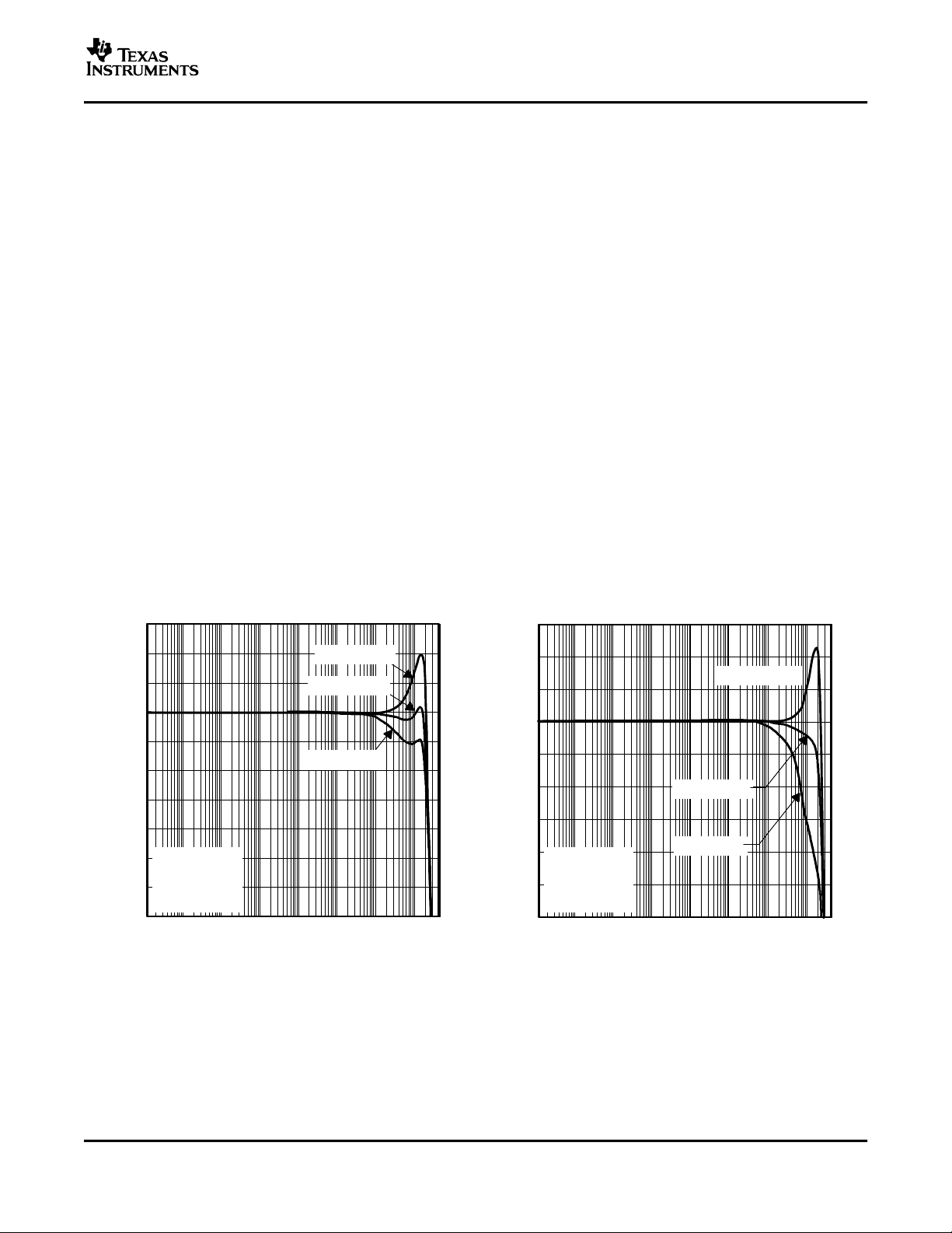
Checking the stability of the amplifier setup is recommended. High frequency oscillations in the megahertz region
can cause undesirable effects in the audio band.
Sometimes, the oscillations can be quite clear. An unexpectedly large draw from the power supply may be an
indication of oscillations. These oscillations can be seen with an oscilloscope. However, if the oscillations are not
obvious, or there is a chance that the system is stable but close to the edge, placing a scope probe with 10 pF of
capacitance can make the oscillations worse, or actually cause them to start.
A network analyzer can be used to determine the inherent stability of a system. An output vs frequency curve
generated by a network analyzer can be a good indicator of stability. At high frequencies, the curve shows
whether a system is oscillating, close to oscillation, or stable. Looking at Figure 27 through Figure 32 , several
different phenomena occur. In one scenario, the system is stable because the high frequency rolloff is smooth
and has no peaking. Increasing R
section). Another scenario shows some peaking at high frequency. If the peaking is 2 dB, the amplifier is stable
as there is still 45 degrees of phase margin. As the peaking increases, the phase margin shrinks, the amplifier
and the system, move closer to instability. The same system that has a 2-dB peak has an increased peak when
a capacitor is added to the output. This indicates the system is either on the verge of oscillation or is oscillating,
and corrective action is required.
decreases the frequency at which this rolloff occurs (see the Resistor Values
F
Figure 27. Normalized Output Response vs Frequency Figure 28. Normalized Output Response vs Frequency
15
Page 16

www.ti.com
10M100k 500M1M 100M10k1k10010
f − Frequency − Hz
Normalized Output Response − dB
−3
−5
−7
−9
−4
−6
−8
−1
0
−2
1
RL = 100 Ω
RL = 25 Ω
VCC = ±15 V
RF = 1 kΩ
Gain = 1 V/V
VI = 200 mV
RL = 50 Ω
RL = 200 Ω
10M100k 500M1M 100M10k1k10010
f − Frequency − Hz
Normalized Output Response − dB
VCC = ±15 V
RF = 1 kΩ
Gain = 2 V/V
VI = 200 mV
−3
−5
−7
−9
−4
−6
−8
−1
0
−2
1
RL = 100 Ω
RL = 25 Ω
RL = 200 Ω
RL = 50 Ω
10M100k 500M1M 100M10k1k10010
f − Frequency − Hz
−5
−6
−2
−1
Output Amplitude − dB
0
3
1
2
−4
−3
VCC = ± 5 V
Gain = 1 V/V
RL = 25 Ω
VI = 200 mV
RF = 1 kΩ
RF = 1.5 kΩ
RF = 620 Ω
10M100k 500M1M 100M10k1k10010
f − Frequency − Hz
1
0
4
5
Output Amplitude − dB
6
9
7
8
2
3
VCC = ± 5 V
Gain = 2 V/V
RL = 25 Ω
VI = 200 mV
RF = 820 Ω
RF = 1.2 kΩ
RF = 510 Ω
TPA6120A2
SLOS431 – MARCH 2004
APPLICATION INFORMATION (continued)
Figure 29. Normalized Output Response vs Frequency Figure 30. Normalized Output Response vs Frequency
Figure 31. Output Amplitude vs Frequency Figure 32. Output Amplitude vs Frequency
PCB Layout
Proper board layout is crucial to getting the maximum performance out of the TPA6120A2.
A ground plane should be used on the board to provide a low inductive ground connection. Having a ground
plane underneath traces adds capacitance, so care must be taken when laying out the ground plane on the
underside of the board (assuming a 2-layer board). The ground plane is necessary on the bottom for thermal
reasons. However, certain areas of the ground plane should be left unfilled. The area underneath the device
where the PowerPAD is soldered down should remain, but there should be no ground plane underneath any of
the input and output pins. This places capacitance directly on those pins and leads to oscillation problems. The
underside ground plane should remain unfilled until it crosses the device side of the input resistors and the
output series resistor. Thermal reliefs should be avoided if possible because of the inductance they introduce.
16
Page 17

www.ti.com
−
+
R
I
R
O
R
L
V
I
Too Long
Too Long
Too Long
Too Long
TPA6120A2
R
F
−
+
R
I
R
O
R
L
V
I
TPA6120A2
Ground as Close to
the Pin as Possible
Short Trace
Before Resistors
R
F
Minimized Length of
the Trace Between
Output Node and R
O
Minimized Length of
Feedback Path
Efficiency of an amplifier
P
L
P
SUP
P
L
V
LRMS
2
R
L
, andV
LRMS
V
P
2
, therefore, P
L
V
P
2
2R
L
per channel
P
SUP
VCCICCavg VCCI
CC(q)
I
CC
avg
1
2
0
V
P
R
L
sin(t) dt
V
P
R
L
[cos(t)]
2
0
V
P
R
L
TPA6120A2
SLOS431 – MARCH 2004
APPLICATION INFORMATION (continued)
Despite the removal of the ground plane in critical areas, stray capacitance can still make its way onto the
sensitive outputs and inputs. Place components as close as possible to the pins and reduce trace lengths. See
Figure 33 and Figure 34 . It is important for the feedback resistor to be extremely close to the pins, as well as the
series output resistor. The input resistor should also be placed close to the pin. If the amplifier is to be driven in a
noninverting configuration, ground the input close to the device so the current has a short, straight path to the
PowerPAD (gnd).
Figure 33. Layout That Can Cause Oscillation
Thermal Considerations
Amplifiers can generate quite a bit of heat. Linear amplifiers, as opposed to Class-D amplifiers, are extremely
inefficient, and heat dissipation can be a problem. There is no one to one relationship between output power and
heat dissipation, so the following equations must be used:
Where
Where
Figure 34. Layout Designed To Reduce Capacitance On Critical Nodes
(1)
(2)
(3)
(4)
17
Page 18
www.ti.com
VP 2 PLR
L
P
SUP
VCCV
P
R
L
VCCI
CC(q)
P
DISS
(1 ) P
SUP
TAMax TJMax ΘJAP
Diss
− Power Dissipation − W
P
D
0
0.2
0.4
0.6
0.8
1
1.2
1.4
1.6
1.8
2
0 0.5 1 1.5 2 2.5 3 3.5
VCC = 15 V , RL = 32
VCC = 15 V ,
RL = 64
VCC = 12 V ,
RL = 64
VCC = 12 V , RL = 32
PO − Output Power − W
Mono Operation
TPA6120A2
SLOS431 – MARCH 2004
APPLICATION INFORMATION (continued)
Therefore,
PL= Power delivered to load (per channel)
P
= Power drawn from power supply
SUP
V
= RMS voltage on the load
LRMS
RL= Load resistance
VP= Peak voltage on the load
ICCavg = Average current drawn from the power supply
ICC(q) = Quiescent current (per channel)
VCC= Power supply voltage (total supply voltage = 30 V if running on a ±15-V power supply
η = Efficiency of a SE amplifier
(5)
(6)
For stereo operation, the efficiency does not change because both P
and P
L
are doubled. This effects the
SUP
amount of power dissipated by the package in the form of heat.
A simple formula for calculating the power dissipated, P
In stereo operation, P
is twice the quantity that is present in mono operation.
SUP
, is shown in Equation 7 :
DISS
The maximum ambient temperature, TA, depends on the heat-sinking ability of the system. θ
whose thermal pad is properly soldered down, is shown in the dissipation rating table.
for a 20-pin DWP,
JA
(7)
(8)
18
Figure 35. Power Dissipation vs Output Power
Page 19

www.ti.com
Application Circuit
DATA
24
23
22
21
20
19
18
17
16
15
5
6
7
8
9
10
11
12
13
14
PCM1792
BCK
SCK
DGND
V
DD
MS
MDI
MC
MDO
RST
AGND2
I
OUT
R−
VCC1
V
COM
L
V
COM
R
I
REF
I
OUT
R+
AGND3R
AGND1
ZEROL
1
2
3
4
ZEROR
MSEL
LRCK
28
27
26
25
VCC2L
AGND3L
I
OUT
L−
I
OUT
L+
5 V
VCC2R
0.1 µF
Controller
10 µF
3.3 V
PCM
Audio
Data
Source
0.1 µF
10 µF
+
+
47 µF
47 µF
5 V
10 µF
10 kΩ
−
+
CF 2.7 nF
R
F
1 k
0.1 µF
10 µF
5 V
+
+
+
+
V−
V+
4
12
13
14
−IND
OUTD
−
+
CF 2.7 nF
R
F
1 k
V−
V+
4
10
9
8
−INC
−
+
CF 2.7 nF
R
F
1 k
V−
V+
4
3
2
1
−
+
CF 2.7 nF
R
F
1 k
V−
V+
4
5
6
7
11
11
11
11
−INB
−INA
OUTA
OUTB
OUTC
−
+
1 k
V
CC−
3
4
5
2
LOUT
0.1 F
V
CC+
LIN−
LIN+
0.1 F
R
O
10
4
−
+
R
F
V
CC−
18
17
16
19
ROUT
0.1 F
V
CC+
RIN−
RIN+
0.1 F
20
1 k
1 k
R
I
R
F
1 k
R
I
1 k
1 k
1 k
R
I
R
F
1 k
R
I
R
F
+
10 µF
0.1 µF
5 V
V+
+
10 µF0.1 µF
−5 V
V−
OPA4134
+
100 µF
10 µF
12 V
V
CC+
+
100 µF10 µF
−12 V
V
CC−
TPA6120A2
+
+
R
O
10
TPA6120A2
SLOS431 – MARCH 2004
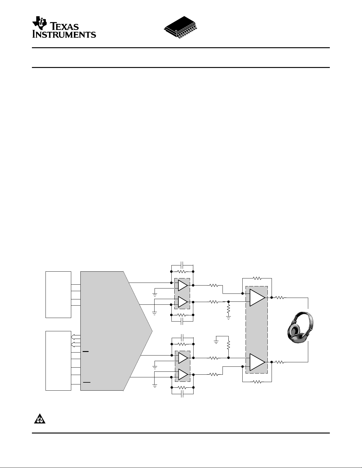
In many applications, the audio source is digital. It must go through a digital-to-analog converter (DAC) so that
traditional analog amplifiers can drive the speakers or headphones.
Figure 36 shows a complete circuit schematic for such a system. The digital audio is fed into a high performance
DAC. The PCM1792, a Burr-Brown product from TI, is a 24-bit, stereo DAC.
The output of the PCM1792 is current, not voltage, so the OPA4134 is used to convert the current input to a
voltage output. The OPA4134, a Burr-Brown product from TI, is a low-noise, high-speed, high-performance
operational amplifier. C
Figure 36 has a cutoff frequency of 59 kHz. All four amplifiers of the OPA4134 are used so the TPA6120A2 can
be driven differentially.
and R
F
Figure 36. Typical Application Circuit
are used to set the cutoff frequency of the filter. The RC combination in
F
19
Page 20

www.ti.com
TPA6120A2
SLOS431 – MARCH 2004
The output of the OPA4134 goes into the TPA6120A2. The TPA6120A2 is configured for use with differential
inputs, stereo use, and a gain of 2V/V. Note that the 0.1-uF capacitors are placed at every supply pin of the
TPA6120A2, as well as the 10-Ω series output resistor.
Each output goes to one channel of a pair of stereo headphones, where the listener enjoys crisp, clean, virtually
noise free music with a dynamic range greater than the human ear is capable of detecting.
20
Page 21

PACKAGE OPTION ADDENDUM
www.ti.com
5-Oct-2007
PACKAGING INFORMATION
Orderable Device Status
TPA6120A2DWP ACTIVE SO
(1)
Package
Type
Power
Package
Drawing
Pins Package
Qty
Eco Plan
DWP 20 25 Green (RoHS &
no Sb/Br)
PAD
TPA6120A2DWPG4 ACTIVE SO
Power
DWP 20 25 Green (RoHS &
no Sb/Br)
PAD
TPA6120A2DWPR ACTIVE SO
Power
DWP 20 2000 Green (RoHS &
no Sb/Br)
PAD
TPA6120A2DWPRG4 ACTIVE SO
Power
DWP 20 2000 Green (RoHS &
no Sb/Br)
PAD
(1)
The marketing status values are defined as follows:
ACTIVE: Product device recommended for new designs.
LIFEBUY: TI has announced that the device will be discontinued, and a lifetime-buy period is in effect.
NRND: Not recommended for new designs. Device is in production to support existing customers, but TI does not recommend using this part in
a new design.
PREVIEW: Device has been announced but is not in production. Samples may or may not be available.
OBSOLETE: TI has discontinued the production of the device.
(2)
Eco Plan - The planned eco-friendly classification: Pb-Free (RoHS), Pb-Free (RoHS Exempt), or Green (RoHS & no Sb/Br) - please check
http://www.ti.com/productcontent for the latest availability information and additional product content details.
TBD: The Pb-Free/Green conversion plan has not been defined.
Pb-Free (RoHS): TI's terms "Lead-Free" or "Pb-Free" mean semiconductor products that are compatible with the current RoHS requirements
for all 6 substances, including the requirement that lead not exceed 0.1% by weight in homogeneous materials. Where designed to be soldered
at high temperatures, TI Pb-Free products are suitable for use in specified lead-free processes.
Pb-Free (RoHS Exempt): This component has a RoHS exemption for either 1) lead-based flip-chip solder bumps used between the die and
package, or 2) lead-based die adhesive used between the die and leadframe. The component is otherwise considered Pb-Free (RoHS
compatible) as defined above.
Green (RoHS & no Sb/Br): TI defines "Green" to mean Pb-Free (RoHS compatible), and free of Bromine (Br) and Antimony (Sb) based flame
retardants (Br or Sb do not exceed 0.1% by weight in homogeneous material)
(2)
Lead/Ball Finish MSL Peak Temp
CU NIPDAU Level-2-260C-1 YEAR
CU NIPDAU Level-2-260C-1 YEAR
CU NIPDAU Level-2-260C-1 YEAR
CU NIPDAU Level-2-260C-1 YEAR
(3)
(3)
MSL, Peak Temp. -- The Moisture Sensitivity Level rating according to the JEDEC industry standard classifications, and peak solder
temperature.
Important Information and Disclaimer:The information provided on this page represents TI's knowledge and belief as of the date that it is
provided. TI bases its knowledge and belief on information provided by third parties, and makes no representation or warranty as to the
accuracy of such information. Efforts are underway to better integrate information from third parties. TI has taken and continues to take
reasonable steps to provide representative and accurate information but may not have conducted destructive testing or chemical analysis on
incoming materials and chemicals. TI and TI suppliers consider certain information to be proprietary, and thus CAS numbers and other limited
information may not be available for release.
In no event shall TI's liability arising out of such information exceed the total purchase price of the TI part(s) at issue in this document sold by TI
to Customer on an annual basis.
Addendum-Page 1
Page 22

PACKAGE MATERIALS INFORMATION
www.ti.com
TAPE AND REEL INFORMATION
19-Mar-2008
*All dimensions are nominal
Device Package
TPA6120A2DWPR SO
Type
Power
PAD
Package
Drawing
DWP 20 2000 330.0 24.4 10.8 13.0 2.7 12.0 24.0 Q1
Pins SPQ Reel
Diameter
(mm)
Reel
Width
W1 (mm)
A0 (mm) B0 (mm) K0 (mm) P1
(mm)W(mm)
Quadrant
Pin1
Pack Materials-Page 1
Page 23

PACKAGE MATERIALS INFORMATION
www.ti.com
19-Mar-2008
*All dimensions are nominal
Device Package Type Package Drawing Pins SPQ Length (mm) Width (mm) Height (mm)
TPA6120A2DWPR SO PowerPAD DWP 20 2000 346.0 346.0 41.0
Pack Materials-Page 2
Page 24

Page 25

Page 26

IMPORTANT NOTICE
Texas Instruments Incorporated and its subsidiaries (TI) reserve the right to make corrections, modifications, enhancements, improvements,
and other changes to its products and services at any time and to discontinue any product or service without notice. Customers should
obtain the latest relevant information before placing orders and should verify that such information is current and complete. All products are
sold subject to TI’s terms and conditions of sale supplied at the time of order acknowledgment.
TI warrants performance of its hardware products to the specifications applicable at the time of sale in accordance with TI’s standard
warranty. Testing and other quality control techniques are used to the extent TI deems necessary to support this warranty. Except where
mandated by government requirements, testing of all parameters of each product is not necessarily performed.
TI assumes no liability for applications assistance or customer product design. Customers are responsible for their products and
applications using TI components. To minimize the risks associated with customer products and applications, customers should provide
adequate design and operating safeguards.
TI does not warrant or represent that any license, either express or implied, is granted under any TI patent right, copyright, mask work right,
or other TI intellectual property right relating to any combination, machine, or process in which TI products or services are used. Information
published by TI regarding third-party products or services does not constitute a license from TI to use such products or services or a
warranty or endorsement thereof. Use of such information may require a license from a third party under the patents or other intellectual
property of the third party, or a license from TI under the patents or other intellectual property of TI.
Reproduction of TI information in TI data books or data sheets is permissible only if reproduction is without alteration and is accompanied
by all associated warranties, conditions, limitations, and notices. Reproduction of this information with alteration is an unfair and deceptive
business practice. TI is not responsible or liable for such altered documentation. Information of third parties may be subject to additional
restrictions.
Resale of TI products or services with statements different from or beyond the parameters stated by TI for that product or service voids all
express and any implied warranties for the associated TI product or service and is an unfair and deceptive business practice. TI is not
responsible or liable for any such statements.
TI products are not authorized for use in safety-critical applications (such as life support) where a failure of the TI product would reasonably
be expected to cause severe personal injury or death, unless officers of the parties have executed an agreement specifically governing
such use. Buyers represent that they have all necessary expertise in the safety and regulatory ramifications of their applications, and
acknowledge and agree that they are solely responsible for all legal, regulatory and safety-related requirements concerning their products
and any use of TI products in such safety-critical applications, notwithstanding any applications-related information or support that may be
provided by TI. Further, Buyers must fully indemnify TI and its representatives against any damages arising out of the use of TI products in
such safety-critical applications.
TI products are neither designed nor intended for use in military/aerospace applications or environments unless the TI products are
specifically designated by TI as military-grade or "enhanced plastic." Only products designated by TI as military-grade meet military
specifications. Buyers acknowledge and agree that any such use of TI products which TI has not designated as military-grade is solely at
the Buyer's risk, and that they are solely responsible for compliance with all legal and regulatory requirements in connection with such use.
TI products are neither designed nor intended for use in automotive applications or environments unless the specific TI products are
designated by TI as compliant with ISO/TS 16949 requirements. Buyers acknowledge and agree that, if they use any non-designated
products in automotive applications, TI will not be responsible for any failure to meet such requirements.
Following are URLs where you can obtain information on other Texas Instruments products and application solutions:
Products Applications
Amplifiers amplifier.ti.com Audio www.ti.com/audio
Data Converters dataconverter.ti.com Automotive www.ti.com/automotive
DSP dsp.ti.com Broadband www.ti.com/broadband
Clocks and Timers www.ti.com/clocks Digital Control www.ti.com/digitalcontrol
Interface interface.ti.com Medical www.ti.com/medical
Logic logic.ti.com Military www.ti.com/military
Power Mgmt power.ti.com Optical Networking www.ti.com/opticalnetwork
Microcontrollers microcontroller.ti.com Security www.ti.com/security
RFID www.ti-rfid.com Telephony www.ti.com/telephony
RF/IF and ZigBee® Solutions www.ti.com/lprf Video & Imaging www.ti.com/video
Mailing Address: Texas Instruments, Post Office Box 655303, Dallas, Texas 75265
Copyright © 2008, Texas Instruments Incorporated
Wireless www.ti.com/wireless
 Loading...