

IN-
IN+
GAIN
ENB
END
GND
VBAT SW PVOUT PVDD
OUT+
OUT-
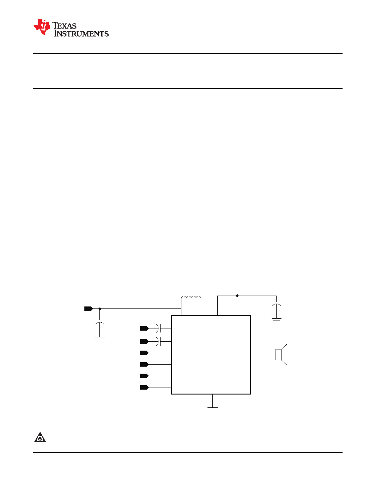
AGC
2.2 Hm
6.8 F - 22 Fm m
TPA2015D1
Differential
Audio Inputs
Gain Control
AGC Control
Boost Enable
Class-D Enable
2.2 F - 10 Fm m
Connected to Supply
TPA2015D1
www.ti.com
SLOS638 –MAY 2010
2 W Constant Output Power Class-D Audio Amplifier With Adaptive Boost Converter and
Battery Tracking SpeakerGuard™ AGC
Check for Samples: TPA2015D1
1
FEATURES
2
• Built-In SpeakerGuardTMAutomatic Gain
Control (AGC) with Enhanced Battery Tracking
– Limits Battery Current Consumption
– Prevents Audio Clipping
• 2 W into 8 Ω Load From 3.6 V Supply (6% THD)
• Integrated Adaptive Boost Converter THD). With 85% typical efficiency, the TPA2015D1
– Increases Efficiency at Low Output Power
• Low Quiescent Current of 1.7 mA from 3.6 V
• Operates From 2.5 V to 5.2 V
• Thermal and Short-Circuit Protection with
Auto Recovery
• Three Gain Settings: 6 dB, 15.5 dB, and 20 dB
• Independent Control for Boost and Class-D
• Pin-to-Pin Compatible with TPA2013D1
• Available in 1.954 mm × 1.954 mm 16-ball
WCSP Package
APPLICATIONS
• Cell Phones, PDA, GPS
• Portable Electronics and Speakers
DESCRIPTION
The TPA2015D1 is a high efficiency Class-D audio
power amplifier with battery-tracking SpeakerGuard™
AGC technology and an integrated adaptive boost
converter that enhances efficiency at low output
power. It drives up to 2 W into an 8 Ω speaker (6%
helps extend battery life when playing audio.
The built-in boost converter generates a 5.5 V supply
voltage for the Class-D amplifier. This provides a
louder audio output than a stand-alone amplifier
directly connected to the battery. The
SpeakerGuardTMAGC adjusts the Class-D gain to
limit battery current and prevent heavy clipping.
The TPA2015D1 has an integrated low-pass filter to
improve the RF rejection and reduce DAC
out-of-band noise, increasing the signal to noise ratio
(SNR).
The TPA2015D1 is available in a space saving
1.954 mm × 1.954 mm, 0.5 mm pitch WCSP package
(YZH).
SIMPLIFIED APPLICATION DIAGRAM
1
2SpeakerGuard is a trademark of Texas Instruments.
PRODUCTION DATA information is current as of publication date.
Products conform to specifications per the terms of the Texas
Instruments standard warranty. Production processing does not
necessarily include testing of all parameters.
Please be aware that an important notice concerning availability, standard warranty, and use in critical applications of Texas
Instruments semiconductor products and disclaimers thereto appears at the end of this data sheet.
Copyright © 2010, Texas Instruments Incorporated
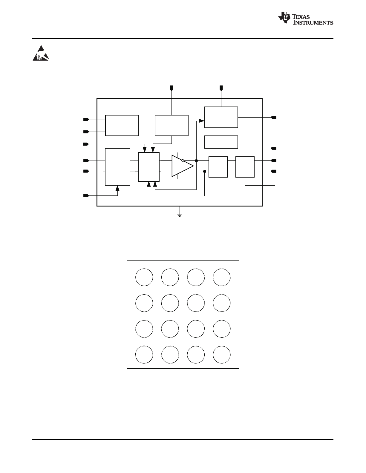
IN-
VBAT
IN+
PVDD
AGND
OUT-
OUT+
GAIN
Oscillator
Boost
Converter
Battery
Monitor
+
–
PWM
H-
Bridge
GND
PVDD
PVOUT
GND
Bias &
Control
END
ENB
SW
Gain
Select:
+20 dB
+15.5 dB
+6 dB
AGC
AGC
PVDD
OUT+
OUT-
GND
GND
GND
VBAT
ENB
SW
AGC
END
IN-
PVOUT
GND
IN+
GAIN
D4
C4
B4
A4
D3
C3
B3
A3
D2
B2
A2
C2
D1
C1
B1
A1
WCSP (YZH)PACKAGE
(TOP VIEW)
SymbolSide
TPA2015D1
SLOS638 –MAY 2010
These devices have limited built-in ESD protection. The leads should be shorted together or the device placed in conductive foam
during storage or handling to prevent electrostatic damage to the MOS gates.
www.ti.com
FUNCTIONAL BLOCK DIAGRAM
DEVICE PINOUT
2 Submit Documentation Feedback Copyright © 2010, Texas Instruments Incorporated
Product Folder Link(s): TPA2015D1
TPA2015D1
www.ti.com
SLOS638 –MAY 2010
PIN FUNCTIONS
PIN INPUT/ OUTPUT/ DESCRIPTION
NAME WCSP
PVDD A1 I Class-D power stage supply voltage.
PVOUT A2 O Boost converter output.
SW A3 I Boost and rectifying switch input.
GND A4, C2, C4, D1 P Ground; all ground balls must be connected for proper functionality.
OUT+ B1 O Positive audio output.
GAIN B2 I Gain selection pin.
AGC B3 I Enable and select AGC.
VBAT B4 P Supply voltage.
OUT– C1 O Negative audio output.
END C3 I Enable for the Class-D amplifier; set to logic high to enable.
IN+ D2 I Positive audio input.
IN– D3 I Negative audio input.
ENB D4 I Enable for the boost converter; set to logic high to enable.
POWER
(I/O/P)
ORDERING INFORMATION
T
A
–40°C to 85°C
PACKAGED DEVICES
16-ball, 1.954mm × 1.954 mm WSCP TPA2015D1YZHR OEN
16-ball, 1.954 mm × 1.954 mm WSCP TPA2015D1YZHT OEN
(1)
PART NUMBER
(1) For the most current package and ordering information, see the Package Option Addendum at the end of this document, or see the TI
Web site at www.ti.com.
(2) The YZH package is only available taped and reeled. The suffix “R” indicates a reel of 3000, the suffix “T” indicates a reel of 250.
(2)
SYMBOL
ABSOLUTE MAXIMUM RATINGS
Over operating free–air temperature range, TA= 25°C (unless otherwise noted)
Supply voltage VBAT –0.3 V 6 V
Input Voltage, V
Output continuous total power dissipation See the Thermal Information Table
Operating free-air temperature range, T
Operating junction temperature range, T
Storage temperature range, T
Minimum load impedance 6 Ω
ESD Protection CDM 500 V
(1) Stresses beyond those listed under absolute maximum ratings may cause permanent damage to the device. These are stress ratings
only, and functional operation of the device at these or any other conditions beyond those indicated under recommended operating
conditions is not implied. Exposure to absolute–maximum–rated conditions for extended periods may affect device reliability.
IN+, IN– –0.3 V VBAT + 0.3 V
I
A
J
STG
HBM 2000 V
MM 100 V
(1)
MIN MAX
–40°C 85°C
–40°C 150°C
–65°C 150°C
Copyright © 2010, Texas Instruments Incorporated Submit Documentation Feedback 3
Product Folder Link(s): TPA2015D1
TPA2015D1
SLOS638 –MAY 2010
www.ti.com
THERMAL INFORMATION
TPA2015D1
THERMAL METRIC
q
JA
q
JC(top)
q
JB
y
JT
y
JB
q
JC(bottom)
Junction-to-ambient thermal resistance
Junction-to-case(top) thermal resistance
Junction-to-board thermal resistance
Junction-to-top characterization parameter
Junction-to-board characterization parameter
Junction-to-case(bottom) thermal resistance
(1) For more information about traditional and new thermal metrics, see the IC Package Thermal Metrics application report, SPRA953.
(2) The junction-to-ambient thermal resistance under natural convection is obtained in a simulation on a JEDEC-standard, high-K board, as
specified in JESD51-7, in an environment described in JESD51-2a.
(3) The junction-to-case (top) thermal resistance is obtained by simulating a cold plate test on the package top. No specific
JEDEC-standard test exists, but a close description can be found in the ANSI SEMI standard G30-88.
(4) The junction-to-board thermal resistance is obtained by simulating in an environment with a ring cold plate fixture to control the PCB
temperature, as described in JESD51-8.
(5) The junction-to-top characterization parameter, yJT, estimates the junction temperature of a device in a real system and is extracted
from the simulation data for obtaining qJA, using a procedure described in JESD51-2a (sections 6 and 7).
(6) The junction-to-board characterization parameter, yJB, estimates the junction temperature of a device in a real system and is extracted
from the simulation data for obtaining qJA, using a procedure described in JESD51-2a (sections 6 and 7).
(7) The junction-to-case (bottom) thermal resistance is obtained by simulating a cold plate test on the exposed (power) pad. No specific
JEDEC standard test exists, but a close description can be found in the ANSI SEMI standard G30-88.
(1)
YZH UNITS
16 PINS
(2)
(3)
(4)
(5)
(6)
(7)
75
22
26
0.5
25
n/a
°C/W
RECOMMENDED OPERATING CONDITIONS
MIN MAX UNIT
Supply voltage, VBAT 2.5 5.2 V
V
V
T
T
High–level input voltage, END, ENB 1.3 V
IH
Low–level input voltage, END, ENB 0.6 V
IL
Operating free-air temperature –40 85 °C
A
Operating junction temperature –40 150 °C
J
ELECTRICAL CHARACTERISTICS
VBAT= 3.6 V, Gain = 6 dB, R
PARAMETER TEST CONDITIONS MIN TYP MAX UNIT
VBAT supply voltage range END = VBAT, ENB = VBAT, AGC options 1, 2, and 3 2.5 5.2
Class-D supply voltage END = ENB = VBAT, boost converter active 5.2 5.8 V
range
Power supply ripple
rejection
Operating quiescent
current
Shutdown quiescent VBAT = 2.5 V to 5.2 V, END = ENB = GND
current
Gain control pin voltage Gain = 15.5 dB (float) 0.4 × VBAT 0.6 × VBAT V
= Float, TA= 25°C, RL= 8 Ω + 33 mH (unless otherwise noted)
AGC
END = 0 V, ENB = VBAT 2.5 5.2
END = VBAT, ENB = VBAT, AGC option 0 2.8 5.2
END = VBAT, ENB = 0 V 3.1 5.25 V
VBAT = 2.5 V to 5.2 V, END = ENB = VBAT 85
VBAT = 2.5 V to 5.2 V, END = VBAT, ENB = 0 V
(pass through mode)
75
END = 0 V, ENB = VBAT 0.5 mA
END = ENB = VBAT 1.7 2.2 mA
0.2 3 mA
Gain = 6 dB (connect to GND) 0 0.25 × VBAT
Gain = 20 dB (connect to VBAT) 0.75 × VBAT
V
dB
4 Submit Documentation Feedback Copyright © 2010, Texas Instruments Incorporated
Product Folder Link(s): TPA2015D1
TPA2015D1
www.ti.com
SLOS638 –MAY 2010
ELECTRICAL CHARACTERISTICS (continued)
VBAT= 3.6 V, Gain = 6 dB, R
PARAMETER TEST CONDITIONS MIN TYP MAX UNIT
AGC control pin voltage V
AGC control pin output
current
Input common-mode IN+, IN–
voltage range
Start-up time Boost converter only 1 4 ms
= Float, TA= 25°C, RL= 8 Ω + 33 mH (unless otherwise noted)
AGC
AGC with no inflection point, R
AGC option 1 (inflection = 3.55 V), R
AGC option 2 (inflection = 3.78 V) , R
AGC option 3 (inflection = 3.96 V) , R
= Open 2
AGC
= 39 kΩ (±5%) 1.36 1.75
AGC
= 27 kΩ (±5%) 0.94 1.2
AGC
= 18 kΩ (±5%) 0 0.825
AGC
37.6 40 42.4 mA
0.6 1.3 V
Boost converter followed by Class-D amplifier 6 10
Class-D amplifier only 5 6
OPERATING CHARACTERISTICS
VBAT= 3.6 V, TA= 25°C, RL= 8 Ω + 33 mH (unless otherwise noted)
PARAMETER TEST CONDITIONS MIN TYP MAX UNIT
BOOST CONVERTER
Boost converter output voltage range, I
PVOUT
I
L
Boost converter input current limit Power supply current 1500 mA
Boost converter start-up current limit 450 mA
h Boost converter efficiency END = 0 V, I
f
BOOST
Boost converter frequency 1.2 MHz
CLASS-D AMPLIFIER
P
V
A
ΔA
V
O
O
V
V
OOS
Output power THD = 1%, VBAT = 3 V, f = 1 kHz 1500 mW
Output peak voltage 5.2 V
Closed-loop voltage gain 0.4 × VBAT < GAIN < 0.6 × VBAT (or float) 15.5 dB
Gain accuracy –0.5 0.5 dB
Output offset voltage 10 mV
Input impedance (per input pin) AV= 15.5 dB 14.9 kΩ
R
IN
Input impedance in shutdown (per input
pin)
Z
O
f
CLASS-D
E
N
THD+N Total harmonic distortion plus noise
AC PSRR dB
Output impedance in shutdown END = 0 V 2 kΩ
Switching frequency 560 600 640 kHz
Noise output voltage A-weighted, GAIN = 15.5 dB 33.4 mV
(1)
AC-Power supply ripple rejection (output
referred)
= 700 mA 5.2 5.8 V
BOOST
= 100 mA constant 88%
PVOUT
THD = 1%, VBAT = 2.5 V, f = 1 kHz 1200
THD = 1%, VBAT = 3.6 V, f = 1 kHz 1700
THD = 1%, VBAT = 3 V, f = 1 kHz,
6 dB crest factor sine burst, no clipping
GAIN < 0.25 × VBAT 6
GAIN > 0.75 × VBAT 20
AV= 6 dB 27.8
AV= 20 dB 10.1
END = 0 V 88.4 kΩ
A-weighted, GAIN = 6 dB 24.8
A-weighted, GAIN = 20 dB 42.4
PO= 100 mW, f = 1 kHz 0.06%
PO= 500 mW, f = 1 kHz 0.07%
200 mVPPripple, f = 217 Hz 75
200 mVPPripple, f = 4 kHz 70
RMS
(1) A-weighted
Copyright © 2010, Texas Instruments Incorporated Submit Documentation Feedback 5
Product Folder Link(s): TPA2015D1
IN+
–
IN–
+
VBAT
1 Fm
1 Fm
2.2 Hm
Load
OUT+
OUT–
Measurement
Output
TPA2015D1
Measurement
Input
–
+
–
+
10 Fm
22 Fm
Supply
GND
30kHz
Low-Pass
Filter
SW PVDD
PVOUT
TPA2015D1
SLOS638 –MAY 2010
OPERATING CHARACTERISTICS (continued)
VBAT= 3.6 V, TA= 25°C, RL= 8 Ω + 33 mH (unless otherwise noted)
PARAMETER TEST CONDITIONS MIN TYP MAX UNIT
f
= 20 Hz, CIN= 1 mF –0.2 –0.1 0
Audio frequency passband ripple dB
AUTOMATIC GAIN CONTROL
AGC gain range 0 20 dB
AGC gain step size 0.5 dB
AGC attack time (gain decrease) 0.026 ms/dB
AGC release time (gain increase) 1600 ms/dB
Limiter threshold voltage VBAT > inflection point 6.15 V
VBAT vs. Limiter slope VBAT < inflection point 3 V/V
AGC inflection point AGC option 2, R
AUDIO
f
= 16 kHz, CIN= 1 mF –0.2 –0.1 0
AUDIO
AGC option 1, R
AGC option 3, R
TEST SET-UP FOR GRAPHS
= 39 kΩ (±5%) 3.55
AGC
= 27 kΩ (±5%) 3.78 V
AGC
= 18 kΩ (±5%) 3.96
AGC
www.ti.com
(1) The 1 µF input capacitors (CI) were shorted for input common-mode voltage measurements.
(2) A 33 mH inductor was placed in series with the load resistor to emulate a small speaker for efficiency measurements.
(3) The 30 kHz low-pass filter is required even if the analyzer has an internal low-pass filter. An R-C low pass filter
(100 Ω, 47 nF) is used on each output for the data sheet graphs.
6 Submit Documentation Feedback Copyright © 2010, Texas Instruments Incorporated
Product Folder Link(s): TPA2015D1
V
BAT
− V
Supply Current − A
2.3 2.6 2.9 3.2 3.5 3.8 4.1 4.4 4.7 5.0
0
2m
4m
6m
8m
10m
Gain = 20 dB
AGC = Float
RL = 8 Ω + 33 µH
Frequency − Hz
Amplitude − dBV
0 2k 4k 6k 8k 10k 12k 14k 16k 18k 20k 22k 24k
−150
−140
−130
−120
−110
−100
−90
−80
Gain = 20 dB
AGC = Float
RL = 8 Ω + 33 µH
No Input Signal
PO − Output Power − W
I
VBAT
− Supply Current − A
0.0 0.5 1.0 1.5 2.0 2.5
0.0
0.2
0.4
0.6
0.8
1.0
V
BAT
= 3.0 V
V
BAT
= 3.6 V
V
BAT
= 4.2 V
Gain = 20 dB
RL = 8 Ω + 33 µH
f = 1 kHz
R
AGC
= Float
VIN − Input Voltage − Vp
V
OUT
− Output Voltage − Vp
0.0 0.5 1.0 1.5 2.0 2.5 3.0 3.5 4.0 4.5
0
1
2
3
4
5
6
V
BAT
= 2.5 V
V
BAT
= 2.7 V
V
BAT
= 3.0 V
V
BAT
= 3.3 V
V
BAT
= 3.6 V
V
BAT
= 4.2 V
V
BAT
= 5.0 V
Gain = 20 dB
RL = 8 Ω + 33 µH
R
AGC
= 27 kΩ
P OutputPower W
O
– –
Efficiency %–
0.01 0.1 1 2
0
20
40
60
80
100
V
BAT
=2.7V
V
BAT
=3.0V
V
BAT
=3.6V
V
BAT
=4.2V
V
BAT
=5.0V
Gain=20dB
R =8 +33 H
L
W m
f=1kHz
AutoPassThrough Boosted
PO − Output Power − W
THD+N − Total Harmonic Distortion + Noise − %
1m 10m 100m 1 4
0.01
0.1
1
10
100
V
BAT
= 2.8 V
V
BAT
= 3.0 V
V
BAT
= 3.6 V
V
BAT
= 4.2 V
V
BAT
= 5.0 V
RL = 8 Ω + 33 µH
R
AGC
= Float, Boost Enabled
Gain = 6 dB, f = 1 kHz
TPA2015D1
www.ti.com
V
= 3.6 V, Gain = 6 dB, CI= 1 µF, C
BAT
otherwise specified.
SPACER
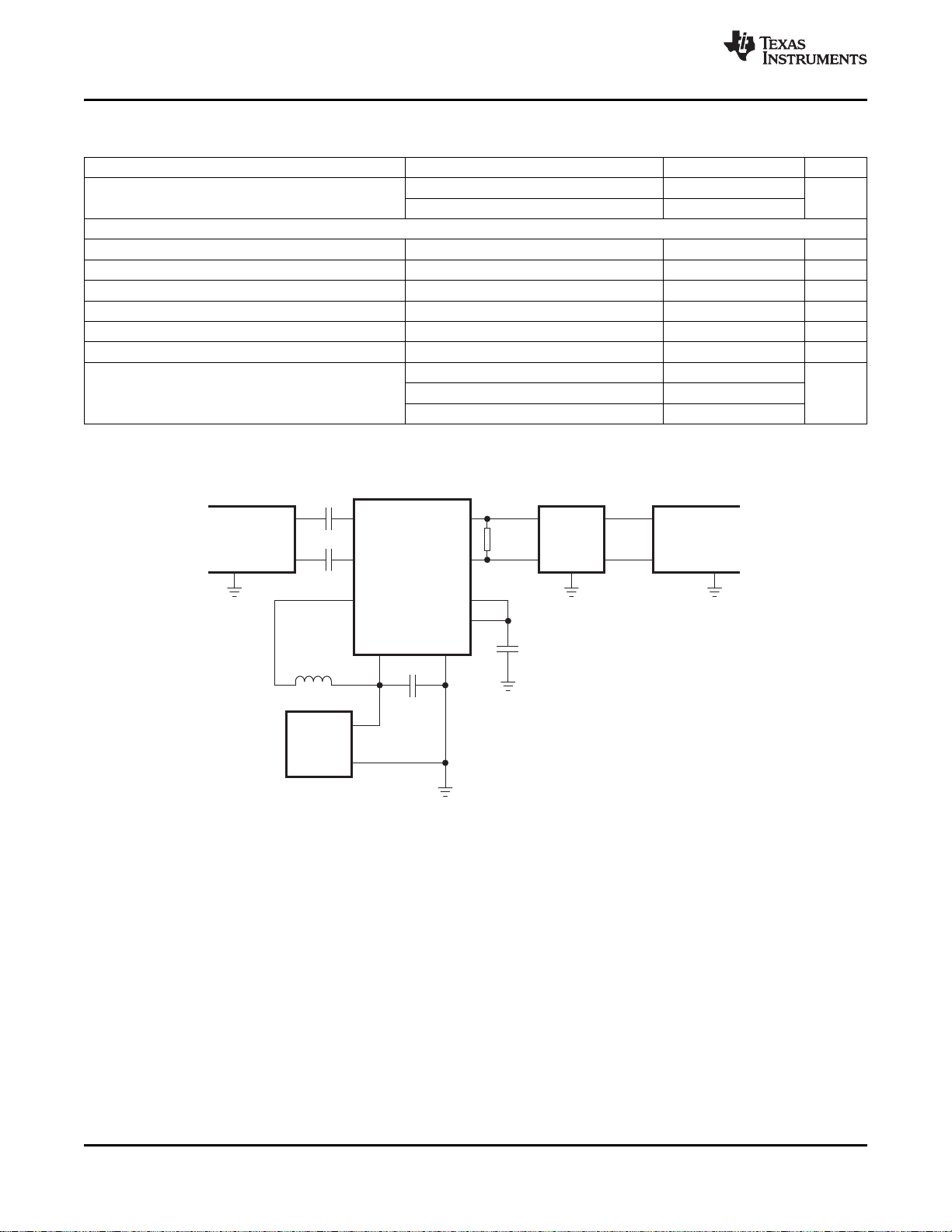
Figure 1. QUIESCENT SUPPLY CURRENT vs SUPPLY Figure 2. A-WEIGHTED OUTPUT NOISE vs FREQUENCY
BOOST
VOLTAGE
TYPICAL CHARACTERISTICS
= 22 µF, L
= 2.2 µH, AGC = Float, ENB = END = V
BOOST
SLOS638 –MAY 2010
, and Load = 8 Ω + 33 µH unless
BAT
Figure 3. SUPPLY CURRENT vs OUTPUT POWER Figure 4. PEAK OUTPUT VOLTAGE vs PEAK INPUT
Figure 5. TOTAL EFFICIENCY vs OUTPUT POWER Figure 6. TOTAL HARMONIC DISTORTION + NOISE vs
Copyright © 2010, Texas Instruments Incorporated Submit Documentation Feedback 7
VOLTAGE
OUTPUT POWER
Product Folder Link(s): TPA2015D1
V
BAT
− Supply Voltage − V
V
OUT
− Maximum Output Voltage − Vp
2.3 2.6 2.9 3.2 3.5 3.8 4.1 4.4 4.7 5.0
1.0
2.0
3.0
4.0
5.0
6.0
R
AGC
= Float
R
AGC
= 39 kΩ
R
AGC
= 27 kΩ
R
AGC
= 18 kΩ
RL = 8 Ω + 33 µH
VIN = 0.45 V
RMS
f = 1 kHz
Gain = 20 dB
f − Frequency − Hz
THD+N − Total Harmonic Distortion + Noise − %
20 100 1k 10k 20k
0.001
0.01
0.1
1
10
Po = 25 mW
Po = 125 mW
Po = 200 mW
V
BAT
= 2.5 V
RL = 8 Ω + 33 µH
R
AGC
= Float
Gain = 6 dB
V
BAT
− Supply Voltage − V
P
O
− Output Power − W
2.3 2.6 2.9 3.2 3.5 3.8 4.1 4.4 4.7 5.0
0.0
0.5
1.0
1.5
2.0
2.5
R
AGC
= Float
R
AGC
= 39 kΩ
R
AGC
= 27 kΩ
R
AGC
= 18 kΩ
RL = 8 Ω + 33 µH
VIN = 0.45 V
RMS
f = 1 kHz
Gain = 20 dB
f − Frequency − Hz
THD+N − Total Harmonic Distortion + Noise − %
20 100 1k 10k 20k
0.001
0.01
0.1
1
10
Po = 50 mW
Po = 250 mW
Po = 500 mW
V
BAT
= 3.6 V
RL = 8 Ω + 33 µH
R
AGC
= Float
Gain = 6 dB
V
BAT
− Supply Voltage − V
I
VBAT
− Supply Current − A
2.3 2.6 2.9 3.2 3.5 3.8 4.1 4.4 4.7 5.0
0.0
0.2
0.4
0.6
0.8
1.0
R
AGC
= Float
R
AGC
= 39 kΩ
R
AGC
= 27 kΩ
R
AGC
= 18 kΩ
RL = 8 Ω + 33 µH
VIN = 0.45 V
RMS
f = 1 kHz
Gain = 20 dB
f − Frequency − Hz
THD+N − Total Harmonic Distortion + Noise − %
20 100 1k 10k 20k
0.001
0.01
0.1
1
10
Po = 100 mW
Po = 500 mW
Po = 1W
V
BAT
= 4.2 V
RL = 8 Ω + 33 µH
R
AGC
= Float
Gain = 6 dB
TPA2015D1
SLOS638 –MAY 2010
TYPICAL CHARACTERISTICS (continued)
V
= 3.6 V, Gain = 6 dB, CI= 1 µF, C
BAT
Load = 8 Ω + 33 µH unless otherwise specified.
SPACER
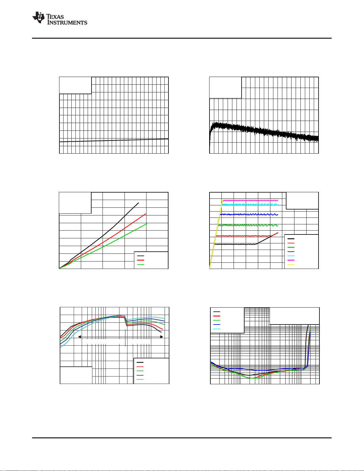
Figure 7. MAXIMUM OUTPUT VOLTAGE vs SUPPLY Figure 8. TOTAL HARMONIC DISTORTION + NOISE vs
VOLTAGE FREQUENCY
BOOST
= 22 µF, L
= 2.2 µH, AGC = Float, ENB = END = V
BOOST
BAT
www.ti.com
, and
Figure 9. OUTPUT POWER vs SUPPLY VOLTAGE Figure 10. TOTAL HARMONIC DISTORTION + NOISE vs
Figure 11. SUPPLY CURRENT vs SUPPLY VOLTAGE Figure 12. TOTAL HARMONIC DISTORTION + NOISE vs
8 Submit Documentation Feedback Copyright © 2010, Texas Instruments Incorporated
FREQUENCY
FREQUENCY
Product Folder Link(s): TPA2015D1

Gain − dB
R
IN
− Input Impedance Per Leg − Ω
0 2 4 6 8 10 12 14 16 18 20
5k
10k
15k
20k
25k
30k
35k
40k
RL = 8 Ω + 33 µH
f − Frequency − Hz
Supply Ripple Rejection − dB
20 100 1k 10k 20k
−100
−80
−60
−40
−20
0
V
BAT
= 2.5 V
V
BAT
= 3.6 V
V
BAT
= 4.2 V
V
BAT
= 5.0 V
RL = 8 Ω + 33 µH
Input Level = 0.2 V
PP
Gain = 6 dB
Output Referred
t − Time − s
V − Voltage − V
0 5m 10m 15m 20m
−2
0
2
4
6
ENB and END
V
OUT+−VOUT−
V
BAT
= 3.6 V
Gain = 6 dB
P
OUT
= 100mW @ 1kHz
RL = 8 Ω + 33 µH
t − Time − s
V − Voltage − V
0 2m 4m 6m 8m 10m
−2
0
2
4
6
ENB and END
V
OUT+−VOUT−
V
BAT
= 3.6 V
Gain = 6 dB
P
OUT
= 100 mW @ 1kHz
RL = 8 Ω + 33 µH
TPA2015D1
www.ti.com
TYPICAL CHARACTERISTICS (continued)
V
= 3.6 V, Gain = 6 dB, CI= 1 µF, C
BAT
Load = 8 Ω + 33 µH unless otherwise specified.
SPACER
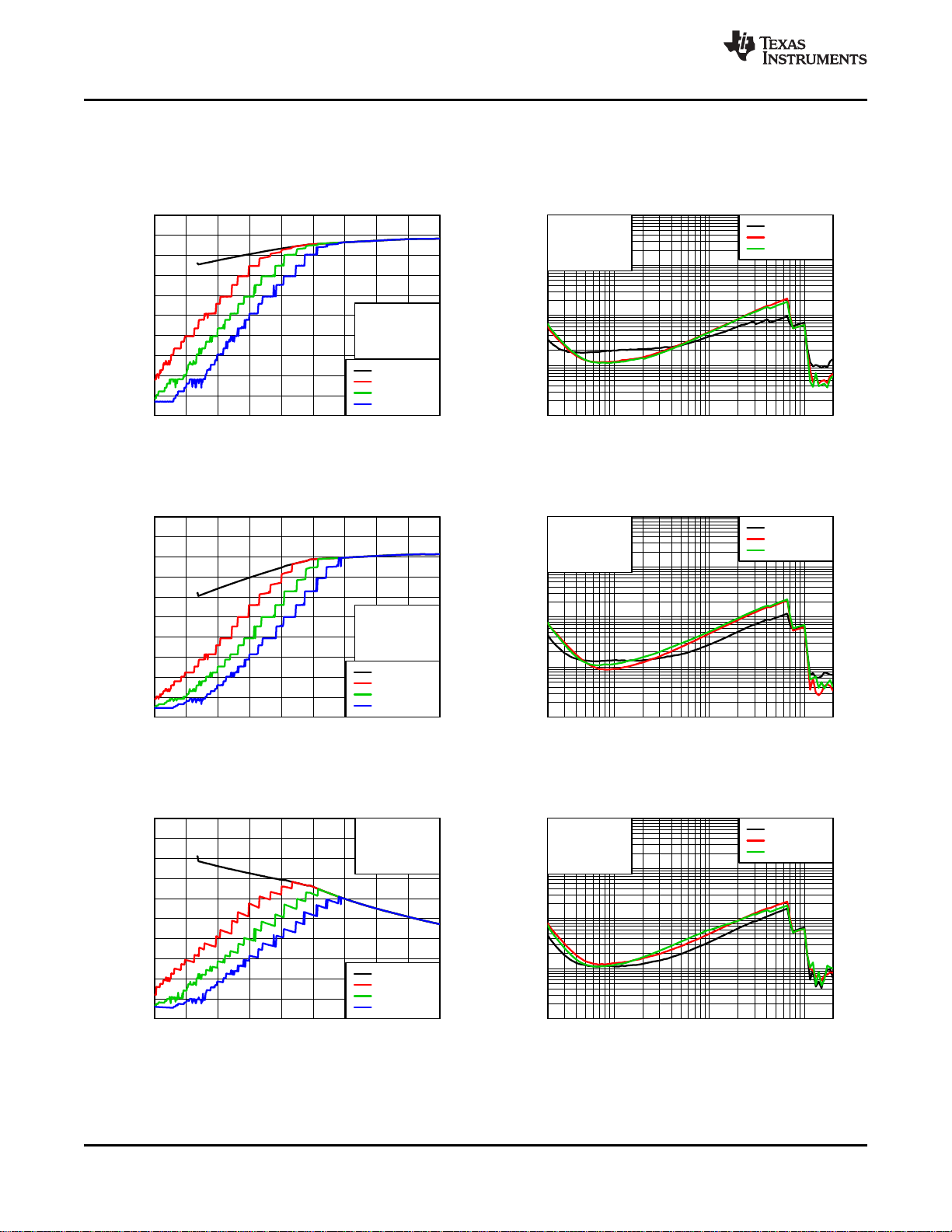
Figure 13. SUPPLY RIPPLE REJECTION vs FREQUENCY Figure 14. INPUT IMPEDANCE (PER INPUT) vs GAIN
BOOST
= 22 µF, L
= 2.2 µH, AGC = Float, ENB = END = V
BOOST
BAT
, and
SLOS638 –MAY 2010
Figure 15. STARTUP TIMING Figure 16. SHUTDOWN TIMING
Copyright © 2010, Texas Instruments Incorporated Submit Documentation Feedback 9
Figure 17. EMC PERFORMANCE Figure 18. EMC PERFORMANCE
PO= 50 mW with 2 INCH SPEAKER CABLE PO= 750 mW with 2 INCH SPEAKER CABLE
Product Folder Link(s): TPA2015D1

IN-
IN+
GAIN
ENB
END
GND
VBAT SW PVOUT PVDD
OUT+
OUT-
AGC
2.2 Hm
6.8 F - 22 Fm m
2.2 F - 10 Fm m
Differential
Audio Inputs
Gain Control
AGC Control
Boost Enable
Class-D Enable
Connected to Supply
TPA2015D1
Single-Ended
Audio Inputs
Gain Control
AGC Control
Boost Enable
Class-D Enable
2.2 Hm
6.8 F - 22 Fm m
2.2 F - 10 Fm m
IN-
IN+
GAIN
ENB
END
GND
VDD SW PVOUT PVDD
OUT+
OUT-
AGC
Connected to Supply
TPA2015D1
TPA2015D1
SLOS638 –MAY 2010
APPLICATION CIRCUIT
Figure 19. Typical Application Schematic with Differential Input Signals
www.ti.com
APPLICATION INFORMATION
10 Submit Documentation Feedback Copyright © 2010, Texas Instruments Incorporated
Figure 20. Typical Application Schematic with Single-Ended Input Signals
Product Folder Link(s): TPA2015D1

TPA2015D1
www.ti.com
SLOS638 –MAY 2010
GLOSSARY
The application section uses the following terms:
Limiter level The maximum output voltage allowed before amplifier gain is automatically reduced.
SpeakerGuard™ TI's trademark name for the automatic gain control technology. It protects speakers by
limiting maximum output power.
Inflection point The battery voltage threshold for reducing the limiter level. If the battery voltage drops
below the inflection point, the limiter level automatically reduces. Although it lowers the
maximum output power, it prevents high battery currents at end-of-charge low battery
voltages.
Battery track The name for the continuous limiter level reduction at battery voltages below the inflection
point.
AGC Automatic gain control.
VBAT The battery supply voltage to the TPA2015D1. The VBAT pin is the input to the boost
converter.
Fixed-gain The nominal audio gain as set by the GAIN pin. If the audio output voltage remains below
the limiter level, the amplifier gain will return to the fixed-gain.
Attack time The rate of AGC gain decrease. The attack time is constant at 0.026 ms/dB.
Release time The rate of AGC gain increase. The release time is constant at 1600 ms/dB.
SPEAKERGUARD™ THEORY OF OPERATION
SpeakerGuard™ protects speakers, improves loudness, and limits peak supply current. If the output audio signal
exceeds the limiter level, then SpeakerGuard™ decreases amplifier gain. The rate of gain decrease, the attack
time, is fixed at 0.026 ms/dB. SpeakerGuard™ increases the gain once the output audio signal is below the
limiter level. The rate of gain increase, the release time, is fixed at 1600 ms/dB. Figure 21 shows this
relationship.
Copyright © 2010, Texas Instruments Incorporated Submit Documentation Feedback 11
Product Folder Link(s): TPA2015D1

LIMITER
LEVEL
INPUT
SIGNAL
GAIN
OUTPUT
SIGNAL
AttackTime
GainStep
ReleaseTime
Inflectionpoint
LimiterLevel(VBAT>inflectionpoint)
LimiterLevel(VBAT=inflectionpoint)
LimiterLevel
SupplyVoltage
TPA2015D1
SLOS638 –MAY 2010
www.ti.com
Figure 21. SpeakerGuard Attack and Release Times
BATTERY TRACKING SPEAKERGUARD™
The TPA2015D1 monitors the battery voltage and the audio signal, automatically decreasing gain when battery
voltage is low and audio output power is high. It finds the optimal gain to maximize loudness and minimize
battery current, providing louder audio and preventing early shutdown at end-of-charge battery voltages.
SpeakerGuard decreases amplifier gain when the audio signal exceeds the limiter level. The limiter level
automatically decreases when the supply voltage (VBAT) is below the inflection point. Figure 22 shows a plot of
the limiter level as a function of the supply voltage.
The limiter level decreases within 60 µs of the supply voltage dropping below the inflection point. Although this is
slightly slower than the 26 µs/dB SpeakerGuard attack time, the difference is audibly imperceptible.
12 Submit Documentation Feedback Copyright © 2010, Texas Instruments Incorporated
Figure 22. Limiter Level vs Supply Voltage
Product Folder Link(s): TPA2015D1
TPA2015D1
www.ti.com
SLOS638 –MAY 2010
Connect a resistor between the AGC pin and ground to set the inflection point, as shown in Table 1. Leave the
AGC pin floating to disable the inflection point, keeping the limiter level constant over all supply voltages.
The maximum limiter level is fixed, as is the slope of the limiter level versus supply voltage. If different values for
maximum limiter level and slope are required, contact your local Texas Instruments representative.
Table 1. AGC Function Table
Function Resistor on AGC pin Inflection Point
Constant limiter level; battery track OFF Floating or connected to VBAT disabled
AGC battery track option 1 39 kΩ 3.55 V
AGC battery track option 2 27 kΩ 3.78 V
AGC battery track option 3 18 kΩ 3.96 V
The audio signal is not affected by the SpeakerGuard™ function unless the peak audio output voltage exceeds
the limiter level. Figure 23 shows the relationship between the audio signal, the limiter level, the supply voltage,
and the supply current.
When VBAT is greater than the inflection point, the limiter level allows the output signal to slightly clip to roughly
6% THD at 2 W into 8 Ω. This is an acceptable peak distortion level for most small-sized portable speakers,
while ensuring maximum loudness from the speaker.
Battery Tracking SpeakerGuard™ Example
Phase 1 Battery discharging normally; supply voltage is above inflection point; audio output remains
below limiter level.
The limiter level remains constant because the supply voltage is greater than the inflection point.
Amplifier gain is constant at fixed-gain as set by the GAIN pin. The audio output remains at a
constant loudness. The boost converter allows the audio output to swing above the battery supply
voltage. Battery supply current increases as supply voltage decreases.
Phase 2 Battery continues to discharge normally; supply voltage decreases below inflection point;
limiter level decreases below audio output.
The limiter level decreases as the battery supply voltage continues to decrease. SpeakerGuard™
lowers amplifier gain, reducing the audio output below the new limiter level. The supply current
decreases due to reduced output power.
Phase 3 Battery supply voltage is constant; audio output remains below limiter level.
The audio output, limiter level, and supply current remain constant as well.
Phase 4 Phone plugged in and battery re-charges; supply voltage increases.
The limiter level increases as the supply voltage increases. SpeakerGuard™ increases amplifier
gain slowly, increasing audio output. Because the TPA2015D1 supply current is proportional to the
PVOUT-to-VBAT ratio, the supply current decreases as battery supply voltage increases.
Phase 5 Battery supply voltage is constant; audio output is below limiter level.
SpeakerGuard™ continues to increase amplifier gain to the fixed-gain as set by the GAIN pin. The
audio output signal increases (slowly due to release time) to original value.
Phase 6 Battery supply voltage is constant; audio output remains below limiter level.
Amplifier gain equal to fixed-gain as set by the GAIN pin. Audio output signal does not change.
Supply current remains constant.
Copyright © 2010, Texas Instruments Incorporated Submit Documentation Feedback 13
Product Folder Link(s): TPA2015D1

LimiterLevel
SupplyVoltage
Class-DVoltage
SupplyCurrent
Phase 1 Phase 2 Phase 3
Phase 4
Phase 5 Phase 6
Inflectionpoint
AudioSignal
V
BAT
− Supply Voltage − V
V
OUT
− Maximum Output Voltage − Vp
2.3 2.6 2.9 3.2 3.5 3.8 4.1 4.4 4.7 5.0
1.0
2.0
3.0
4.0
5.0
6.0
VIN = 0.707 V
RMS
VIN = 0.564 V
RMS
VIN = 0.475 V
RMS
RL = 8 Ω + 33 µH
R
AGC
= 27 kΩ
f = 1 kHz
Gain = 15.5 dB
TPA2015D1
SLOS638 –MAY 2010
Figure 23. Relationship Between Supply Voltage, Current, Limiter Level, and Output Audio Signal
www.ti.com
SpeakerGuard with Varying Input Levels
SpeakerGuard protects speakers by decreasing gain during large output transients. Figure 24 shows the
maximum output voltage at different input voltage levels. The load is 8 Ω and the gain is 15.5 dB (6 V/V).
Figure 24. MAXIMUM OUTPUT VOLTAGE vs SUPPLY VOLTAGE
A 0.707 V
sine-wave input signal forces the output voltage to 4.242 V
RMS
, or 6.0 V
RMS
. Above 3.9 V supply,
PEAK
the boost converter voltage sags due to high output current, resulting in a peak Class-D output voltage of about
5.4 V. As the supply voltage decreases below 3.9 V, the limiter level decreases. This causes the gain to
decrease, and the peak Class-D output voltage lowers.
With a 0.564 V
input signal, the peak Class-D output voltage is 4.78 V. When the supply voltage is above
RMS
3.45 V, the output voltage remains below the limiter level, and the gain stays at 15.5 dB. Once the supply drops
below 3.45 V, the limiter level decreases below 4.78 V, and SpeakerGuard decreases the gain.
The same rationale applies to the 0.475 V
input signal. Although the supply voltage may be below the
RMS
inflection point, audio gain does not decrease until the Class-D output voltage is above the limiter level.
14 Submit Documentation Feedback Copyright © 2010, Texas Instruments Incorporated
Product Folder Link(s): TPA2015D1

TPA2015D1
www.ti.com
SLOS638 –MAY 2010
SPEAKER LOAD LIMITATION
Speakers are non-linear loads with varying impedance (magnitude and phase) over the audio frequency. A
portion of speaker load current can flow back into the boost converter output via the Class-D output H-bridge
high-side device. This is dependent on the speaker's phase change over frequency, and the audio signal
amplitude and frequency content.
Most portable speakers have limited phase change at the resonant frequency, typically no more than 40 or 50
degrees. To avoid excess flow-back current, use speakers with limited phase change. Otherwise, flow-back
current could exceed the 10 mA rating of the boost converter voltage clamp and drive the PVOUT voltage above
the absolute maximum recommended operational voltage.
Confirm proper operation by connecting the speaker to the TPA2015D1 and driving it at maximum output swing.
Observe the PVOUT voltage with an oscilloscope. In the unlikely event the PVOUT voltage exceeds 6.5 V, add a
6.8 V Zener diode between PVOUT and ground to ensure the TPA2015D1 operates properly.
The amplifier has thermal overload protection and decatives if the die temperature exceeds 150°C. It
automatically reactivates once die temperature returns below 150°C. Built-in output over-current protection
deactivates the amplifier if the speaker load becomes short-circuited. The amplifier automatically restarts within
200 ms after the over-current event. Although the TPA2015D1 Class-D output can withstand a short between
OUT+ and OUT-, do not connect either output directly to GND, PVDD, or VBAT as this could damage the device.
WARNING
Do not connect OUT+ or OUT- directly to GND, PVDD, or VBAT as this could
damage the Class-D output stage.
Copyright © 2010, Texas Instruments Incorporated Submit Documentation Feedback 15
Product Folder Link(s): TPA2015D1

TPA2015D1
SLOS638 –MAY 2010
www.ti.com
FULLY DIFFERENTIAL CLASS-D AMPLIFIER
The TPA2015D1 uses a fully differential amplifier with differential inputs and outputs. The differential output
voltage equals the differential input multiplied by the amplifier gain. The TPA2015D1 can also be used with a
single-ended input. However, using differential input signals when in a noisy environment, like a wireless
handset, ensures maximum system noise rejection.
Advantages of Fully Differential Amplifiers
• Mid-supply bypass capacitor, C
– The fully differential amplifier does not require a mid-supply bypass capacitor. Any shift in the mid-supply
affects both positive and negative channels equally and cancels at the differential output.
• Improved RF-immunity:
– GSM handsets save power by turning on and shutting off the RF transmitter at a rate of 217 Hz. This
217 Hz burst often couples to audio amplifier input and output traces causing frame-rate noise. Fully
differential amplifiers cancel frame-rate noise better than non-differential amplifiers.
• Input-coupling capacitors not required, but recommended:
– The fully differential amplifier allows the inputs to be biased at voltages other than mid-supply (PVDD/2).
The TPA2015D1 inputs can be biased anywhere within the common mode input voltage range, as listed in
the OPERATING CHARACTERISTICS table. If the inputs are biased outside of that range, then
input-coupling capacitors are required.
– Note that without input coupling capacitors, any dc offset from the audio source will be modulated by the
AGC. This could cause artifacts in the audio output signal. Perform listening tests to determine if direct
input coupling is acceptable.
The TPA2015D1 has 3 selectable fixed-gains: 6 dB, 15.5 dB, and 20 dB. Connect the GAIN pin as shown in
Table 2.
BYPASS
, not required:
Table 2. Amplifier Fixed-Gain
Connect GAIN Pin to Amplifier Gain
GND 6 dB
No Connection (Floating) 15.5 dB
VBAT 20 dB
Improved Class-D Efficiency
The TPA2015D1 output stage uses a modulation technique that modulates the PWM output only on one side of
the differential output, leaving the other side held at ground. Although the differential output voltage is
undistorted, each output appears as a half-wave rectified signal.
This technique reduces output switching losses and improves overall amplifier efficiency. Figure 25 shows how
OUT+, OUT-, and the differential output voltages appear on an oscilloscope.
16 Submit Documentation Feedback Copyright © 2010, Texas Instruments Incorporated
Product Folder Link(s): TPA2015D1

t − Time − s
V − Voltage − V
0.0 0.5 1.0 1.5 2.0
−6
−4
−2
0
2
4
6
8
10
12
PVOUT
V
OUT+−VOUT−
V
BAT
= 3.6 V
Gain = 20 dB
AGC = Float
RL = 8 Ω + 33 µH
TPA2015D1
www.ti.com
FILTERED OUTPUT WAVEFORMS
SLOS638 –MAY 2010
Figure 25.
ADAPTIVE BOOST CONVERTER
The TPA2015D1 consists of an adaptive boost converter and a Class-D amplifier. The boost converter takes the
supply voltage, VBAT, and increases it to a higher output voltage, PVOUT. PVOUT drives the supply voltage of
the Class-D amplifier, PVDD. This improves loudness over non-boosted solutions.
The boost converter is adaptive and activates automatically depending on the output audio signal amplitude.
When the peak output audio signal exceeds a preset voltage threshold, the boost converter is enabled, and the
voltage at PVOUT is 5.5 V. When the audio output voltage is lower than the threshold voltage, the boost
deactivates automatically. The boost activation threshold voltage is not user programmable. It is optimized to
prevent clipping while maximizing system efficiency.
The boost converter can be forcibly deactivated by setting the ENB pin to logic-low. When the boost is
deactivated, PVOUT is equal to the supply voltage (VBAT) minus the I x R drop across the inductor and boost
converter pass transistor.
A timer prevents the input signal from modulating the PVOUT voltage within the audio frequency range,
eliminating the potential for audible artifacts on the Class-D output.
Figure 26 shows how the adaptive boost modulates with a typical audio signal. By automatically deactivating the
boost converter and passing VBAT to PVOUT, the TPA2015D1 efficiency is improved at low output power.
The primary external components for the boost converter are the inductor and the boost capacitor. The inductor
stores current, and the boost capacitor stores charge. As the Class-D amplifier depletes the charge in the boost
capacitor, the boost inductor replenishes charge with its stored current. The cycle of charge and discharge
occurs frequently enough to keep PVOUT within its minimum and maximum voltage specification.
Copyright © 2010, Texas Instruments Incorporated Submit Documentation Feedback 17
Figure 26. ADAPTIVE BOOST CONVERTER with TYPICAL MUSIC PLAYBACK
Product Folder Link(s): TPA2015D1

L PVD D
PVDD
I = I
VBAT 0.8
æ ö
´
ç ÷
´
è ø
TPA2015D1
SLOS638 –MAY 2010
www.ti.com
The boost converter design is optimized for driving the integrated Class-D amplifier only. It lacks protection
circuitry recommended for driving loads other than the integrated Class-D amplifier.
Boost Converter Overvoltage Protection
The TPA2015D1 internal boost converter operates in a discontinuous mode to improve the efficiency at light
loads. The boost converter has overvoltage protection that disables the boost converter if the output voltage
exceeds 5.8 V. If current is forced into the PVOUT terminal, the voltage clamp will sink up to 10 mA. If more than
10 mA is forced into PVOUT, then the PVOUT voltage will increase. Refer to the SPEAKER LOAD LIMITATION
section for details.
Boost Converter Component Section
Boost Terms
The following is a list of terms and definitions used in the boost equations found later in this document.
C Minimum boost capacitance required for a given ripple voltage on PVOUT.
L Boost inductor.
f
BOOST
I
PVDD
I
L
Switching frequency of the boost converter.
Current pulled by the Class-D amplifier from the boost converter.
Average current through the boost inductor.
PVDD Supply voltage for the Class-D amplifier. (Voltage generated by the boost converter output.)
(PVOUT)
VBAT Supply voltage to the IC.
ΔI
L
Ripple current through the inductor.
ΔV Ripple voltage on PVOUT.
Boost Converter Inductor Selection
Working inductance decreases as inductor current and temperature increases. If the drop in working inductance
is severe enough, it may cause the boost converter to become unstable, or cause the TPA2015D1 to reach its
current limit at a lower output voltage than expected. Inductor vendors specify currents at which inductor values
decrease by a specific percentage. This can vary by 10% to 35%. Inductance is also affected by dc current and
temperature.
Inductor Equations
Inductor current rating is determined by the requirements of the load. The inductance is determined by two
factors: the minimum value required for stability and the maximum ripple current permitted in the application.
Use Equation 1 to determine the required current rating. Equation 1 shows the approximate relationship between
the average inductor current, IL, to the load current, load voltage, and input voltage (I
respectively). Insert I
, PVDD, and VBAT into Equation 1 and solve for IL. The inductor must maintain at least
PVDD
90% of its initial inductance value at this current.
WARNING
Use a minimum working inductance of 1.3 mH. Lower values may damage the
inductor.
, PVDD, and VBAT,
PVDD
(1)
18 Submit Documentation Feedback Copyright © 2010, Texas Instruments Incorporated
Product Folder Link(s): TPA2015D1

L BOOST
VBAT (PVDD VBAT)
L =
I PVDD
´ -
D ´ ¦ ´
PVDD
BOOST
I (PVDD VBAT)
C = 1.5
V PVDD
´ -
´
D ´ ¦ ´
TPA2015D1
www.ti.com
SLOS638 –MAY 2010
Ripple current, ΔIL, is peak-to-peak variation in inductor current. Smaller ripple current reduces core losses in the
inductor and reduces the potential for EMI. Use Equation 2 to determine the value of the inductor, L. Equation 2
shows the relationship between inductance L, VBAT, PVDD, the switching frequency, f
, and ΔIL. Insert the
BOOST
maximum acceptable ripple current into Equation 2 and solve for L.
(2)
ΔILis inversely proportional to L. Minimize ΔILas much as is necessary for a specific application. Increase the
inductance to reduce the ripple current. Do not use greater than 4.7 mH, as this prevents the boost converter
from responding to fast output current changes properly. If using above 3.3 µH, then use at least 10 µF
capacitance on PVOUT to ensure boost converter stability.
The typical inductor value range for the TPA2015D1 is 2.2 mH to 3.3 µH. Select an inductor with less than 0.5 Ω
dc resistance, DCR. Higher DCR reduces total efficiency due to an increase in voltage drop across the inductor.
Table 3. Sample Inductors
L SUPPLIER COMPONENT CODE SIZE DCR TYP I
(mH) (L×W×H mm) (mΩ) (A)
2.2 Chilisin CLCN252012T-2R2M-N 2.5 x 2.0 x 1.2 105 1.2
Electronics Corp.
2.2 Toko 1239AS-H-2R2N=P2 2.5 × 2.0 × 1.2 96 2.3 6.8 – 22 µF / 10 V
2.2 Coilcraft XFL4020-222MEC 4.0 x 4.0 x 2.15 22 3.5
3.3 Toko 1239AS-H-3R3N=P2 2.5 × 2.0 × 1.2 160 2.0
3.3 Coilcraft XFL4020-332MEC 4.0 x 4.0 x 2.15 35 2.8
MAX C RANGE
SAT
4.7 – 22 µF / 16 V
10 – 22 µF / 10 V
Boost Converter Capacitor Selection
The value of the boost capacitor is determined by the minimum value of working capacitance required for stability
and the maximum voltage ripple allowed on PVDD in the application. Working capacitance refers to the available
capacitance after derating the capacitor value for DC bias, temperature, and aging.
Do not use any component with a working capacitance less than 4.7 mF. This corresponds to a 4.7 µF / 16 V
capacitor, or a 6.8 µF / 10 V capacitor. Do not use above 22 µF capacitance as it will reduce the boost converter
response time to large output current transients.
Equation 3 shows the relationship between the boost capacitance, C, to load current, load voltage, ripple voltage,
input voltage, and switching frequency (I
Insert the maximum allowed ripple voltage into Equation 3 and solve for C. The 1.5 multiplier accounts for
capacitance loss due to applied dc voltage and temperature for X5R and X7R ceramic capacitors.
, PVDD, ΔV, VBAT, and f
PVDD
BOOST
respectively).
(3)
Copyright © 2010, Texas Instruments Incorporated Submit Documentation Feedback 19
Product Folder Link(s): TPA2015D1

( )
x x
c
I I
1
f =
2 R Cp
JA
1 1
θ = = = 153 C/W
Derating Factor 0.0065
°
JA J JA Dmax
MAX = T MAX = P = 150 - 153(0.34) = 97.98 Cq q °
TPA2015D1
SLOS638 –MAY 2010
www.ti.com
COMPONENTS LOCATION AND SELECTION
Decoupling Capacitors
The TPA2015D1 is a high-performance Class-D audio amplifier that requires adequate power supply decoupling.
Adequate power supply decoupling to ensures that the efficiency is high and total harmonic distortion (THD) is
low.
Place a low equivalent-series-resistance (ESR) ceramic capacitor, typically 0.1 mF, within 2 mm of the VBAT ball.
This choice of capacitor and placement helps with higher frequency transients, spikes, or digital hash on the line.
Additionally, placing this decoupling capacitor close to the TPA2015D1 is important, as any parasitic resistance
or inductance between the device and the capacitor causes efficiency loss. In addition to the 0.1 µF ceramic
capacitor, place a 2.2 mF to 10 mF capacitor on the VBAT supply trace. This larger capacitor acts as a charge
reservoir, providing energy faster than the board supply, thus helping to prevent any droop in the supply voltage.
Input Capacitors
Input audio DC decoupling capacitors are recommended. The input audio DC decoupling capacitors prevents the
AGC from changing the gain due to audio DAC output offset. The input capacitors and TPA2015D1 input
impedance form a high-pass filter with the corner frequency, fC, determined in Equation 4.
Any mismatch in capacitance between the two inputs will cause a mismatch in the corner frequencies. Severe
mismatch may also cause turn-on pop noise. Choose capacitors with a tolerance of ±10% or better.
(4)
EFFICIENCY AND THERMAL INFORMATION
It is important to operate the TPA2015D1 at temperatures lower than its maximum operating temperature. The
maximum ambient temperature depends on the heat-sinking ability of the PCB system. The derating factor for
the package is shown in the dissipation rating table. Converting this to qJAfor the WCSP package:
(5)
Given qJAof 153°C/W, the maximum allowable junction temperature of 150°C, and the internal dissipation of
0.34 W for 1.7 W, 8 Ω load, 3.6 V supply, the maximum ambient temperature is calculated as:
(6)
Equation 6 shows that the calculated maximum ambient temperature is 98°C at maximum power dissipation with
at 3.6 V supply and 8 Ω a load. The TPA2015D3 is designed with thermal protection that turns the device off
when the junction temperature surpasses 150°C to prevent damage to the IC.
20 Submit Documentation Feedback Copyright © 2010, Texas Instruments Incorporated
Product Folder Link(s): TPA2015D1

2.2 Hm
2.2 F – 10 Fm m
6.8 F – 22 Fm m
IN-
IN+
GAIN
ENB
END
GND
VDD SW PVOUT PVDD
OUT+
OUT-
TPA2015D1
Differential
Audio Inputs
Connected to Supply
Gain Control
Boost Enable
Class-D Enable
AGCAGC Control
47 nF
100 W
TPA2015D1
www.ti.com
SLOS638 –MAY 2010
OPERATION WITH DACS AND CODECS
Large ripple voltages can be present at the output of ΔΣ DACs and CODECs, just above the audio frequency
(e.g: 80 kHz with a 300 mVPP). This out-of-band noise is due to the noise shaping of the delta-sigma modulator in
the DAC.
Some Class-D amplifiers have higher output noise when used in combination with these DACs and CODECs.
This is because out-of-band noise from the CODEC/DAC mixes with the Class-D switching frequencies in the
audio amplifier input stage.
The TPA2015D1 has a built-in low-pass filter that reduces the out-of-band noise and RF noise, filtering
out-of-band frequencies that could degrade in-band noise performance. This built-in filter also prevents AGC
errors due to out-of-band noise. The TPA2015D1 AGC calculates gain based on input signal amplitude only.
If driving the TPA2015D1 input with 4th-order or higher ΔΣ DACs or CODECs, add an R-C low pass filter at each
of the audio inputs (IN+ and IN-) of the TPA2015D1 to ensure best performance. The recommended resistor
value is 100 Ω and the capacitor value of 47 nF.
FILTER FREE OPERATION AND FERRITE BEAD FILTERS
The TPA2015D1 is designed to minimize RF emissions. For more information about RF emissions and filtering
requirements, See SLOA145 for further information.
PACKAGE DIMENSIONS
The TPA2015D1 uses a 16-ball, 0.5 mm pitch WCSP package. The die length (D) and width (E) correspond to
the package mechanical drawing at the end of the datasheet.
Copyright © 2010, Texas Instruments Incorporated Submit Documentation Feedback 21
Figure 27. Reducing Out-of-Band DAC Noise with External Input Filter
Table 4. Package Dimensions
Dimension D E
Max 1984 µm 1984 µm
Typ 1954 µm 1954 µm
Min 1924 µm 1924 µm
Product Folder Link(s): TPA2015D1

Copper
Trace Width
Solder Mask
Thickness
Solder
Pad Width
Solder Mask
Opening
Copper Trace
Thickness
TPA2015D1
SLOS638 –MAY 2010
www.ti.com
BOARD LAYOUT
In making the pad size for the WCSP balls, it is recommended that the layout use nonsolder mask defined
(NSMD) land.
With this method, the solder mask opening is made larger than the desired land area, and the opening size is
defined by the copper pad width. Figure 28 and Table 5 show the appropriate diameters for a WCSP layout.
Figure 28. Land Pattern Dimensions
Table 5. Land Pattern Dimensions
SOLDER PAD COPPER SOLDER MASK
DEFINITIONS PAD OPENING THICKNESS OPENING THICKNESS
Nonsolder mask 275 mm 275 mm x 275 mm Sq.
defined (NSMD) (+0.0, -25 mm) (rounded corners)
(1) Circuit traces from NSMD defined PWB lands should be 75 mm to 100 mm wide in the exposed area inside the solder mask opening.
Wider trace widths reduce device stand off and impact reliability.
(2) Best reliability results are achieved when the PWB laminate glass transition temperature is above the operating the range of the
intended application.
(3) Recommend solder paste is Type 3 or Type 4.
(4) For a PWB using a Ni/Au surface finish, the gold thickness should be less 0.5 mm to avoid a reduction in thermal fatigue performance.
(5) Solder mask thickness should be less than 20 mm on top of the copper circuit pattern
(6) Best solder stencil performance is achieved using laser cut stencils with electro polishing. Use of chemically etched stencils results in
inferior solder paste volume control.
(7) Trace routing away from WCSP device should be balanced in X and Y directions to avoid unintentional component movement due to
solder wetting forces.
375 mm (+0.0, -25 mm) 1 oz max (32 mm) 125 mm thick
(5)
COPPER STENCIL
(1) (2) (3) (4)
(6) (7)
STENCIL
TRACE WIDTH
Recommended trace width at the solder balls is 75 mm to 100 mm to prevent solder wicking onto wider PCB
traces. For high current pins (SW, GND, OUT+, OUT–, PVOUT, and PVDD) of the TPA2015D1, use 100 mm
trace widths at the solder balls and at least 500 mm PCB traces to ensure proper performance and output power
for the device. For low current pins (IN–, IN+, END, ENB, GAIN, AGC, VBAT) of the TPA2015D1, use 75 mm to
100 mm trace widths at the solder balls. Run IN- and IN+ traces side-by-side (and if possible, same length) to
maximize common-mode noise cancellation.
22 Submit Documentation Feedback Copyright © 2010, Texas Instruments Incorporated
Product Folder Link(s): TPA2015D1

PACKAGE OPTION ADDENDUM
www.ti.com
10-Jun-2010
PACKAGING INFORMATION
Orderable Device
TPA2015D1YZHR ACTIVE DSBGA YZH 16 3000 Green (RoHS
TPA2015D1YZHT ACTIVE DSBGA YZH 16 250 Green (RoHS
(1)
The marketing status values are defined as follows:
ACTIVE: Product device recommended for new designs.
LIFEBUY: TI has announced that the device will be discontinued, and a lifetime-buy period is in effect.
NRND: Not recommended for new designs. Device is in production to support existing customers, but TI does not recommend using this part in a new design.
PREVIEW: Device has been announced but is not in production. Samples may or may not be available.
OBSOLETE: TI has discontinued the production of the device.
Status
(1)
Package Type Package
Drawing
Pins Package Qty
Eco Plan
& no Sb/Br)
& no Sb/Br)
(2)
Lead/
Ball Finish
SNAGCU Level-1-260C-UNLIM Request Free Samples
SNAGCU Level-1-260C-UNLIM Purchase Samples
MSL Peak Temp
(3)
Samples
(Requires Login)
(2)
Eco Plan - The planned eco-friendly classification: Pb-Free (RoHS), Pb-Free (RoHS Exempt), or Green (RoHS & no Sb/Br) - please check http://www.ti.com/productcontent for the latest availability
information and additional product content details.
TBD: The Pb-Free/Green conversion plan has not been defined.
Pb-Free (RoHS): TI's terms "Lead-Free" or "Pb-Free" mean semiconductor products that are compatible with the current RoHS requirements for all 6 substances, including the requirement that
lead not exceed 0.1% by weight in homogeneous materials. Where designed to be soldered at high temperatures, TI Pb-Free products are suitable for use in specified lead-free processes.
Pb-Free (RoHS Exempt): This component has a RoHS exemption for either 1) lead-based flip-chip solder bumps used between the die and package, or 2) lead-based die adhesive used between
the die and leadframe. The component is otherwise considered Pb-Free (RoHS compatible) as defined above.
Green (RoHS & no Sb/Br): TI defines "Green" to mean Pb-Free (RoHS compatible), and free of Bromine (Br) and Antimony (Sb) based flame retardants (Br or Sb do not exceed 0.1% by weight
in homogeneous material)
(3)
MSL, Peak Temp. -- The Moisture Sensitivity Level rating according to the JEDEC industry standard classifications, and peak solder temperature.
Important Information and Disclaimer:The information provided on this page represents TI's knowledge and belief as of the date that it is provided. TI bases its knowledge and belief on information
provided by third parties, and makes no representation or warranty as to the accuracy of such information. Efforts are underway to better integrate information from third parties. TI has taken and
continues to take reasonable steps to provide representative and accurate information but may not have conducted destructive testing or chemical analysis on incoming materials and chemicals.
TI and TI suppliers consider certain information to be proprietary, and thus CAS numbers and other limited information may not be available for release.
In no event shall TI's liability arising out of such information exceed the total purchase price of the TI part(s) at issue in this document sold by TI to Customer on an annual basis.
Addendum-Page 1


IMPORTANT NOTICE
Texas Instruments Incorporated and its subsidiaries (TI) reserve the right to make corrections, modifications, enhancements, improvements,
and other changes to its products and services at any time and to discontinue any product or service without notice. Customers should
obtain the latest relevant information before placing orders and should verify that such information is current and complete. All products are
sold subject to TI’s terms and conditions of sale supplied at the time of order acknowledgment.
TI warrants performance of its hardware products to the specifications applicable at the time of sale in accordance with TI’s standard
warranty. Testing and other quality control techniques are used to the extent TI deems necessary to support this warranty. Except where
mandated by government requirements, testing of all parameters of each product is not necessarily performed.
TI assumes no liability for applications assistance or customer product design. Customers are responsible for their products and
applications using TI components. To minimize the risks associated with customer products and applications, customers should provide
adequate design and operating safeguards.
TI does not warrant or represent that any license, either express or implied, is granted under any TI patent right, copyright, mask work right,
or other TI intellectual property right relating to any combination, machine, or process in which TI products or services are used. Information
published by TI regarding third-party products or services does not constitute a license from TI to use such products or services or a
warranty or endorsement thereof. Use of such information may require a license from a third party under the patents or other intellectual
property of the third party, or a license from TI under the patents or other intellectual property of TI.
Reproduction of TI information in TI data books or data sheets is permissible only if reproduction is without alteration and is accompanied
by all associated warranties, conditions, limitations, and notices. Reproduction of this information with alteration is an unfair and deceptive
business practice. TI is not responsible or liable for such altered documentation. Information of third parties may be subject to additional
restrictions.
Resale of TI products or services with statements different from or beyond the parameters stated by TI for that product or service voids all
express and any implied warranties for the associated TI product or service and is an unfair and deceptive business practice. TI is not
responsible or liable for any such statements.
TI products are not authorized for use in safety-critical applications (such as life support) where a failure of the TI product would reasonably
be expected to cause severe personal injury or death, unless officers of the parties have executed an agreement specifically governing
such use. Buyers represent that they have all necessary expertise in the safety and regulatory ramifications of their applications, and
acknowledge and agree that they are solely responsible for all legal, regulatory and safety-related requirements concerning their products
and any use of TI products in such safety-critical applications, notwithstanding any applications-related information or support that may be
provided by TI. Further, Buyers must fully indemnify TI and its representatives against any damages arising out of the use of TI products in
such safety-critical applications.
TI products are neither designed nor intended for use in military/aerospace applications or environments unless the TI products are
specifically designated by TI as military-grade or "enhanced plastic." Only products designated by TI as military-grade meet military
specifications. Buyers acknowledge and agree that any such use of TI products which TI has not designated as military-grade is solely at
the Buyer's risk, and that they are solely responsible for compliance with all legal and regulatory requirements in connection with such use.
TI products are neither designed nor intended for use in automotive applications or environments unless the specific TI products are
designated by TI as compliant with ISO/TS 16949 requirements. Buyers acknowledge and agree that, if they use any non-designated
products in automotive applications, TI will not be responsible for any failure to meet such requirements.
Following are URLs where you can obtain information on other Texas Instruments products and application solutions:
Products Applications
Amplifiers amplifier.ti.com Audio www.ti.com/audio
Data Converters dataconverter.ti.com Automotive www.ti.com/automotive
DLP® Products www.dlp.com Communications and www.ti.com/communications
DSP dsp.ti.com Computers and www.ti.com/computers
Clocks and Timers www.ti.com/clocks Consumer Electronics www.ti.com/consumer-apps
Interface interface.ti.com Energy www.ti.com/energy
Logic logic.ti.com Industrial www.ti.com/industrial
Power Mgmt power.ti.com Medical www.ti.com/medical
Microcontrollers microcontroller.ti.com Security www.ti.com/security
RFID www.ti-rfid.com Space, Avionics & www.ti.com/space-avionics-defense
RF/IF and ZigBee® Solutions www.ti.com/lprf Video and Imaging www.ti.com/video
Mailing Address: Texas Instruments, Post Office Box 655303, Dallas, Texas 75265
Copyright © 2010, Texas Instruments Incorporated
Telecom
Peripherals
Defense
Wireless www.ti.com/wireless-apps
 Loading...