

RTJYZH
www.ti.com
VDD = 3.6 V, 10%
0
0.50
1
1.50
2
2.50
4 9 14 19 24 29 34
P
O
− Output Power − W
RL − Load Resistance − W
WCSP Thermally Limited Region
VDD = 5 V, 1%
VDD = 2.5 V, 1%
VDD = 2.5 V, 10%
VDD = 3.6 V, 1%
VDD = 3.6 V, 10%
SLOS438C – DECEMBER 2004 – REVISED MARCH 2007
2.1 W/CH STEREO FILTER-FREE CLASS-D AUDIO POWER AMPLIFIER
FEATURES APPLICATIONS
• Output Power By Package:
– QFN:
– 2.1 W/Ch Into 4 Ω at 5 V
– 1.4 W/Ch Into 8 Ω at 5 V
– 720 mW/Ch Into 8 Ω at 3.6 V
– WCSP:
– 1.2 W/Ch Into 4 Ω at 5 V
(1)
– 1.3 W/Ch Into 8 Ω at 5 V
– 720 mW/Ch Into 8 Ω at 3.6 V
• Only Two External Components Required
• Power Supply Range: 2.5 V to 5.5 V
• Independent Shutdown Control for Each
Channel The TPA2012D2 features independent shutdown
• Selectable Gain of 6, 12, 18, and 24 dB
• Internal Pulldown Resistor On Shutdown Pins
• High PSRR: 77 dB at 217 Hz
• Fast Startup Time (3.5 ms)
• Low Supply Current
• Low Shutdown Current
• Short-Circuit and Thermal Protection
• Space Saving Packages
– 2,01 mm X 2,01 mm NanoFree™ WCSP
(YZH)
– 4 mm X 4 mm Thin QFN (RTJ) with
PowerPAD™
(1)
Thermally limited
• Wireless or Cellular Handsets and PDAs
• Portable DVD Player
• Notebook PC
• Portable Radio
• Portable Gaming
• Educational Toys
• USB Speakers
DESCRIPTION
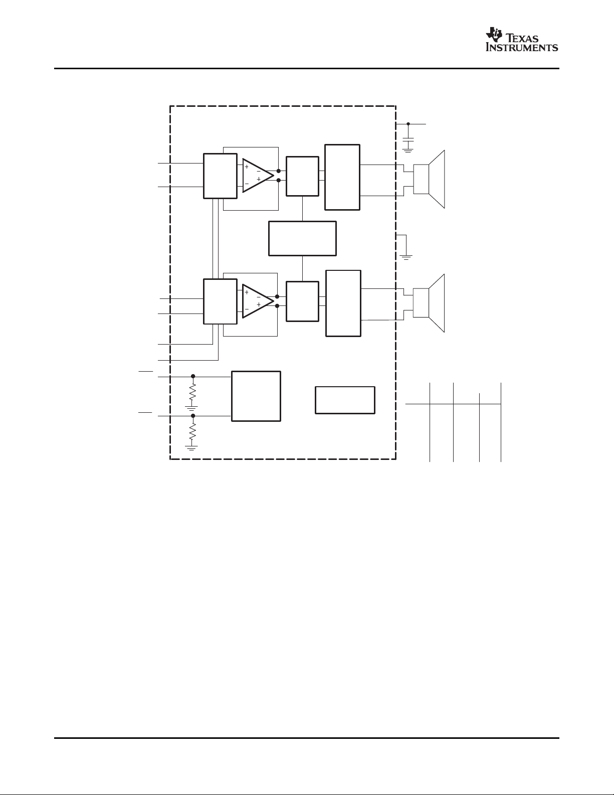
The TPA2012D2 is a stereo, filter-free, Class-D
audio amplifier (class-D amp) available in a WCSP,
QFN, or PWP package. The TPA2012D2 only
requires two external components for operation.
controls for each channel. The gain can be selected
to 6, 12, 18, or 24 dB utilizing the G0 and G1 gain
select pins. High PSRR and differential architecture
provide increased immunity to noise and RF
rectification. In addition to these features, a fast
startup time and small package size make the
TPA2012D2 class-D amp an ideal choice for both
cellular handsets and PDAs.
TPA2012D2
Please be aware that an important notice concerning availability, standard warranty, and use in critical applications of Texas Instruments semiconductor products and disclaimers thereto appears at the end of this data sheet.
NanoFree, PowerPAD are trademarks of Texas Instruments.
PRODUCTION DATA information is current as of publication date.
Products conform to specifications per the terms of the Texas
Instruments standard warranty. Production processing does not
necessarily include testing of all parameters.
Copyright © 2004–2007, Texas Instruments Incorporated
www.ti.com
TPA2012D2
SLOS438C – DECEMBER 2004 – REVISED MARCH 2007
These devices have limited built-in ESD protection. The leads should be shorted together or the device placed in conductive foam
during storage or handling to prevent electrostatic damage to the MOS gates.
DESCRIPTION (CONTINUED)
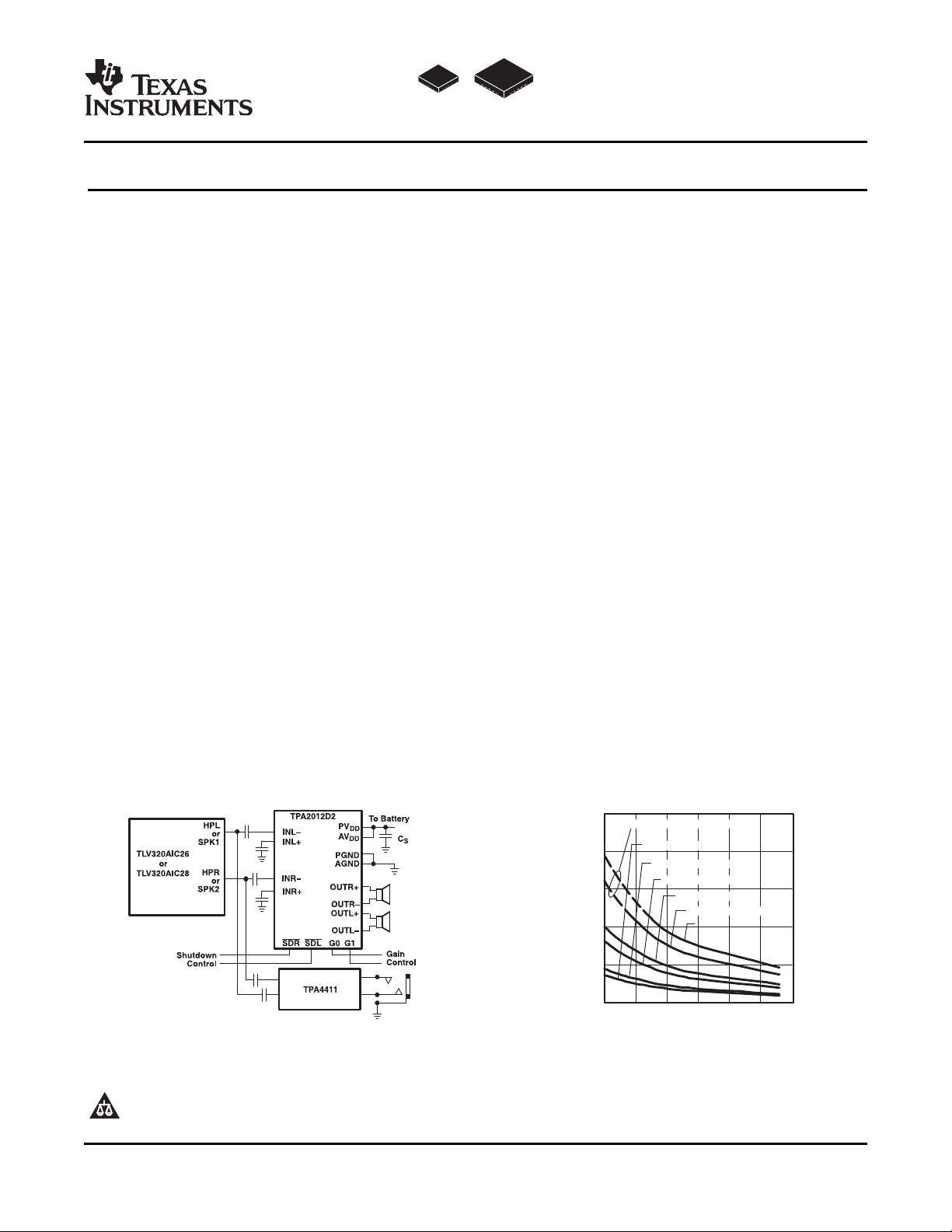
The TPA2012D2 is capable of driving 1.4 W/Ch at 5 V or 720 mW/Ch at 3.6 V into 8 Ω . The TPA2012D2 is also
capable of driving 4 Ω . The TPA2012D2 is thermally limited in WCSP and may not achieve 2.1 W/Ch for 4 Ω .
The maximum output power in the WCSP is determined by the ability of the circuit board to remove heat. The
output power versus load resistance graph below shows thermally limited region of the WCSP in relation to the
QFN package. The TPA2012D2 provides thermal and short circuit protection.
AVAILABLE OPTIONS
T
A
–40 ° C to 85 ° C
2 mm x 2 mm, 16-ball WCSP (YZH) TPA2012D2YZH AKR
4 mm x 4 mm, 20-pin QFN (RTJ) TPA2012D2RTJ AKS
ABSOLUTE MAXIMUM RATINGS
over operating free-air temperature (unless otherwise noted)
V
V
T
T
T
(1) Stresses beyond those listed under absolute maximum ratings may cause permanent damage to the device. These are stress ratings
Supply voltage, AVDD, PVDD
SS
Input voltage –0.3 to V
I
Continuous total power dissipation See Dissipation Rating Table
Operating free-air temperature range –40 to 85 ° C
A
Operating junction temperature range –40 to 150 ° C
J
Storage temperature range –65 to 85 ° C
stg
only, and functional operation of the device at these or any other conditions beyond those indicated under recommended operating
conditions is not implied. Exposure to absolute-maximum-rated conditions for extended periods may affect device reliability.
In active mode –0.3 to 6.0 V
In shutdown mode –0.3 to 7.0 V
PACKAGE PART NUMBER SYMBOL
(1)
VALUE UNIT
+ 0.3 V
DD
DISSIPATION RATING TABLE
PACKAGE
RTJ 5.2 W 41.6 mW/ ° C 3.12 W 2.7 W
YZH 1.2 W 9.12 mW/ ° C 690 mW 600 mW
(1) This data was taken using 2 oz trace and copper pad that is soldered directly to a JEDEC standard 4-layer 3 in × 3 in PCB.
TA= 25 ° C DERATING TA= 75 ° C TA= 85 ° C
POWER RATING
(1)
FACTOR POWER RATING POWER RATING
RECOMMENDED OPERATING CONDITIONS
V
V
V
T
2
Supply voltage AVDD, PVDD 2.5 5.5 V
SS
High-level input voltage SDL, SDR, G0, G1 1.3 V
IH
Low-level input voltage SDL, SDR, G0, G1 0.35 V
IL
Operating free-air temperature ÷ 40 85 ° C
A
Submit Documentation Feedback
MIN MAX UNIT
www.ti.com
TPA2012D2
SLOS438C – DECEMBER 2004 – REVISED MARCH 2007
ELECTRICAL CHARACTERISTICS
TA= 25 ° C (unless otherwise noted)
PARAMETER TEST CONDITIONS MIN TYP MAX UNIT
|V
| Output offset voltage (measured differentially) 5 25 mV
OO
PSRR Power supply rejection ratio VDD= 2.5 to 5.5 V –75 –55 dB
V
icm
Common-mode input voltage 0.5 VDD–0.8 V
CMRR Common-mode rejection ration –69 –50 dB
|IIH| High-level input current VDD= 5.5 V, VI= V
|IIL| Low-level input current VDD= 5.5 V, VI= 0 V 5 µ A
I
DD
r
DS(on)
Supply current
Static drain-source on-state resistance VDD= 3.6 V 570 m Ω
Output impedance in shutdown mode V
f
(sw)
Switching frequency VDD= 2.5 V to 5.5 V 250 300 350 kHz
Closed-loop voltage gain dB
Inputs ac grounded, AV= 6 dB,
VDD= 2.5 to 5.5 V
Inputs shorted together,
VDD= 2.5 to 5.5 V
DD
50 µ A
VDD= 5.5 V, No load or output filter 6 9
VDD= 3.6 V, No load or output filter 5 7.5 mA
VDD= 2.5 V, No load or output filter 4 6
Shutdown mode 1.5 µ A
VDD= 5.5 V 500
VDD= 2.5 V 700
= 0.35 V 2 k Ω
( SDR, SDL)
G0, G1 = 0.35 V 5.5 6 6.5
G0 = VDD, G1 = 0.35 V 11.5 12 12.5
G0 = 0.35 V, G1 = V
G0, G1 = V
DD
DD
17.5 18 18.5
23.5 24 24.5
OPERATING CHARACTERISTICS
TA= 25 ° C, RL= 8 Ω (unless otherwise noted)
PARAMETER TEST CONDITIONS MIN TYP MAX UNIT
P
O
Output power (per channel) VDD= 3.6 V, f = 1 kHz, THD = 10% 0.72 W
RL= 8 Ω
RL= 4 Ω VDD= 5.0 V, f = 1 kHz, THD = 10% 2.1
THD+N Total harmonic distortion plus noise
PO= 1 W, VDD= 5 V, AV= 6 dB, f = 1 kHz 0.14%
PO= 0.5 W, VDD= 5 V, AV= 6 dB, f = 1 kHz 0.11%
Channel crosstalk f = 1 kHz –85 dB
k
SVR
Supply ripple rejection ratio dB
VDD= 5 V, AV= 6 dB, f = 217 Hz –77
VDD= 3.6 V, AV= 6 dB, f = 217 Hz –73
CMRR Common mode rejection ratio VDD= 3.6 V, VIC= 1 Vpp, f = 217 Hz –69 dB
Av = 6 dB 28.1
Input impedance k Ω
Av = 12 dB 17.3
Av = 18 dB 9.8
Av = 24 dB 5.2
Start-up time from shutdown VDD= 3.6 V 3.5 ms
V
n
Output voltage noise µ V
VDD= 3.6 V, f = 20 to 20 kHz,
Inputs are ac grounded, AV= 6 dB
VDD= 5.0 V, f = 1 kHz, THD = 10% 1.4
No weighting 35
A weighting 27
Submit Documentation Feedback
3
www.ti.com
to Battery
V
DD
OUTR+
GND
SDR
INR+
300 k
C
S
Right Input
SDL
300 k
G0
OUTR−
OUTL+
OUTL−
G1
INR−
INL+
INL−
G1
Gain
G0
V/V dB
Left Input
Gain
Adjust
PWM
Gain
Adjust
PWM
H −
Bridge
H −
Bridge
Internal
Oscillator
Bias
Circuitry
6
12
18
24
2
4
8
16
0
1
0
1
0
0
1
1
Short−Circuit
Protection
TPA2012D2
SLOS438C – DECEMBER 2004 – REVISED MARCH 2007
BLOCK DIAGRAM
4
Submit Documentation Feedback
www.ti.com
AGND
OUTL+
PGND
INL− G1
G0
SDR
INL+
AVDD
SDL
OUTR−
INR−
PVDD
OUTR+
OUTL−
INR+
A1
B1
C1
D1
A2 A3 A4
AGND
INR+
INR−
INL+
INL−
G0
OUTR+
PVDD
PGND
OUTR−
NC
SDL
SDR
AVDD
NC
OUTL+
PVDD
PGND
G1
OUTL−
20 19 18 17 16
6 7 8 9 10
1
2
3
4
5
15
14
13
12
11
SLOS438C – DECEMBER 2004 – REVISED MARCH 2007
Terminal Functions
TERMINAL
NAME QFN WCSP
INR+ 16 D1 I Right channel positive input
INR- 17 C1 I Right channel negative input
INL+ 20 A1 I Left channel positive input
INL- 19 B1 I Left channel negative input
SDR 8 B3 I Right channel shutdown terminal (active low)
SDL 7 B4 I Left channel shutdown terminal (active low)
G0 15 C2 I Gain select (LSB)
G1 1 B2 I Gain select (MSB)
PVDD 3, 13 A2 I Power supply (Must be same voltage as AVDD)
AVDD 9 D2 I Analog supply (Must be same voltage as PVDD)
PGND 4, 12 C4 I Power ground
AGND 18 C3 I Analog ground
OUTR+ 14 D3 O Right channel positive differential output
OUTR- 11 D4 O Right channel negative differential output
OUTL+ 2 A3 O Left channel positive differential output
OUTL- 5 A4 O Left channel negative differential output
NC 6, 10 N/A No internal connection
Thermal Pad Connect the thermal pad of QFN or PWP package to PCB GND
I/O DESCRIPTION
TPA2012D2
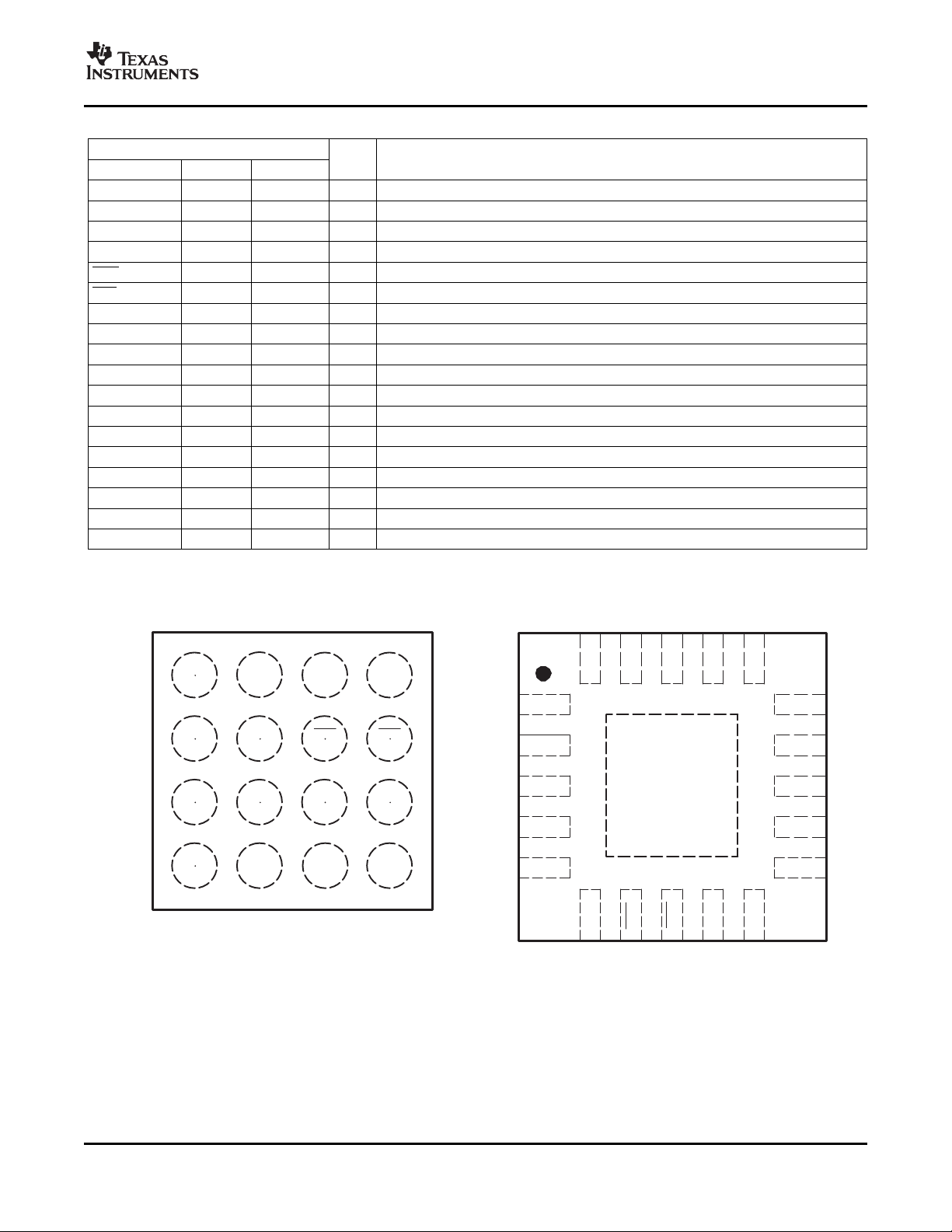
WCSP PIN OUT RTJ PIN OUT
TOP VIEW TOP VIEW
Submit Documentation Feedback
5
www.ti.com
TPA2012D2
IN+
IN-
OUT+
OUT-
V
DD
GND
C
I
C
I
R
I
R
I
Measurement
Output
+
-
1 Fm
+
-
Load
30kHz
Filter
LowPass
Measurement
Input
+
-
V
DD
TPA2012D2
SLOS438C – DECEMBER 2004 – REVISED MARCH 2007
TEST SET-UP FOR GRAPHS (per channel)
(1) CIwas Shorted for any Common-Mode input voltage measurement.
(2) A 33- µ H inductor was placed in series with the load resistor to emulate a small speaker for efficiency measurements.
(3) The 30–kHz low–pass filter is required even if the analyzer has an internal low–pass filter. An RC low pass filter (100
Ω , 47 nF) is used on each output for the data sheet graphs.
Submit Documentation Feedback
6
www.ti.com
0.01
0.1
1
10
0.01 0.1 1 3
2.5 V
3.6 V
THD+N − Total Harmonic Distortion + Noise − %
PO − Output Power − W
RL = 8 ,
f = 1 kHz,
AV 24 dB
5 V
20
0.01
0.1
1
10
20
0.01
0.1
1 4
2.5 V
3.6 V
5 V
PO − Output Power − W
RL = 4 ,
f = 1 kHz,
AV 24 dB
THD+N − Total Harmonic Distortion + Noise − %
0.01
0.1
1
10
20
0.01 0.1 1 3
2.5 V
3.6 V
PO − Output Power − W
RL = 8 ,
f = 1 kHz,
AV 6 dB
5 V
THD+N − Total Harmonic Distortion + Noise − %
0.1
1
20 100 1 k
10 k
20 k
f − Frequency − Hz
VDD = 2.5 V,
RL = 4 W,
CI = 1 mF,
AV = 6 dB
0.01
120 mW
350 mW
240 mW
THD+N − Total Harmonic Distortion + Noise − %
0.1
1
20 100 1 k 10 k 20 k
f − Frequency − Hz
VDD = 2.5 V,
RL = 8 W,
CI = 1 mF,
AV = 6 dB
0.01
90 mW
180 mW
THD+N − Total Harmonic Distortion + Noise − %
260 mW
0.01
0.1
1
10
20
0.01
0.1
1 4
2.5 V
3.6 V
5 V
PO − Output Power − W
RL = 4 ,
f = 1 kHz,
AV 6 dB
THD+N − Total Harmonic Distortion + Noise − %
0.1
1
20 100 1 k 10 k 20 k
f − Frequency − Hz
VDD = 3.6 V,
RL = 4 W,
CI = 1 mF,
AV = 6 dB
0.01
275 mW
550 mW
825 mW
THD+N − Total Harmonic Distortion + Noise − %
0.1
1
20 100 1 k 10 k 20 k
f − Frequency − Hz
VDD = 3.6 V,
RL = 8 W,
CI = 1 mF,
AV = 6 dB
0.01
190 mW
375 mW
560 mW
THD+N − Total Harmonic Distortion + Noise − %
0.1
1
20 100 1 k 10 k 20 k
f − Frequency − Hz
VDD = 5 V,
RL = 4 W,
CI = 1 mF,
AV = 6 dB
0.01
550 mW
1.1 W
1.65 W
THD+N − Total Harmonic Distortion + Noise − %
TPA2012D2
SLOS438C – DECEMBER 2004 – REVISED MARCH 2007
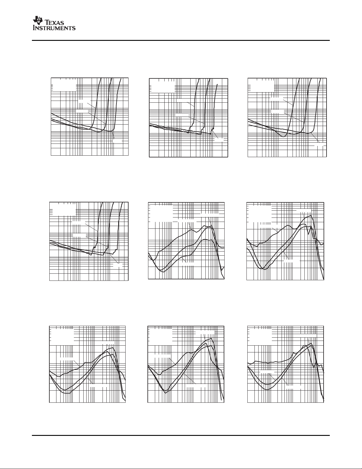
TYPICAL CHARACTERISTICS
TOTAL HARMONIC DISTORTION TOTAL HARMONIC DISTORTION TOTAL HARMONIC DISTORTION
vs vs vs
OUTPUT POWER OUTPUT POWER OUTPUT POWER
Figure 1. Figure 2. Figure 3.
TOTAL HARMONIC DISTORTION TOTAL HARMONIC DISTORTION TOTAL HARMONIC DISTORTION
vs vs vs
OUTPUT POWER FREQUENCY FREQUENCY
TOTAL HARMONIC DISTORTION TOTAL HARMONIC DISTORTION TOTAL HARMONIC DISTORTION
Figure 4. Figure 5. Figure 6.
vs vs vs
FREQUENCY FREQUENCY FREQUENCY
Figure 7. Figure 8. Figure 9.
Submit Documentation Feedback
7
www.ti.com
NoOutputFilter
0.1
1
20 100 1 k 10 k 20 k
f − Frequency − Hz
VDD = 5 V,
RL = 8 W,
CI = 1 mF,
AV = 6 dB
0.01
380 mW
775 mW
1.16 W
THD+N − Total Harmonic Distortion + Noise − %
0
1
2
3
4
5
6
0 1 2 3 4 5
VDD = 5 V
VDD = 3.6 V
VDD = 2.5 V
I
DD
− Supply Current − mA
VSD − Shutdown Voltage − V
0
200
400
600
800
1000
1200
0 0.2 0.4 0.6 0.8 1 1.2 1.4 1.6 1.8 2 2.2
VDD = 2.5 V, RL = 4 W, 33 mH
IDD is for Both Channels
VDD = 5 V, RL = 4 W, 33 mH
VDD = 3.6 V, RL = 4 W, 33 mH
I
DD
− Supply Current − mA
PO − Output Power/Channel − W
I
DD
− Supply Current − mA
0
100
200
300
400
500
600
700
800
0 0.2 0.4 0.6 0.8 1 1.2 1.4 1.6
VDD = 2.5 V, RL = 8 W, 33 mH
VDD = 3.6 V, RL = 8 W, 33 mH
VDD = 5 V, RL = 8 W, 33 mH
IDD is for Both Channels
PO − Output Power/Channel − W
−140
−120
−100
−80
−60
−40
−20
0
100 1 k 10 k
f − Frequency − Hz
2.5 V R to L
5 V R to L
3.6 V R to L
5 V L to R
3.6 V L to R
Crosstalk − dB
RI = 8 W
20 k20
2.5 V L to R
−120
−100
−80
−60
−40
−20
0
100 1 k 10 k
f − Frequency − Hz
2.5 V R to L
2.5 V L to R
3.6 V L to R
3.6 V R to L
5 V R to L
5 V L to R
Crosstalk − dB
20 k20
RI = 4 W
−100
−90
−80
−70
−60
−50
−40
−30
100 1 k 10 k
Inputs AC, Grounded,
CI = 1 mF,
RI = 4 W,
AV = 6 dB
VDD = 2.7 V
VDD = 5 V
VDD = 3.6 V
PSRR − Power Supply Rejection Ratio − dB
f − Frequency − Hz
20 k20
−100
−90
−80
−70
−60
−50
−40
−30
100 1 k 10 k
Inputs AC Grounded,
CI = 1 mF,
RI = 8 W,
AV = 6 dB
VDD = 2.7 V
VDD = 5 V
VDD = 3.6 V
PSRR − Power Supply Rejection Ratio − dB
f − Frequency − Hz
20 k20
TPA2012D2
SLOS438C – DECEMBER 2004 – REVISED MARCH 2007
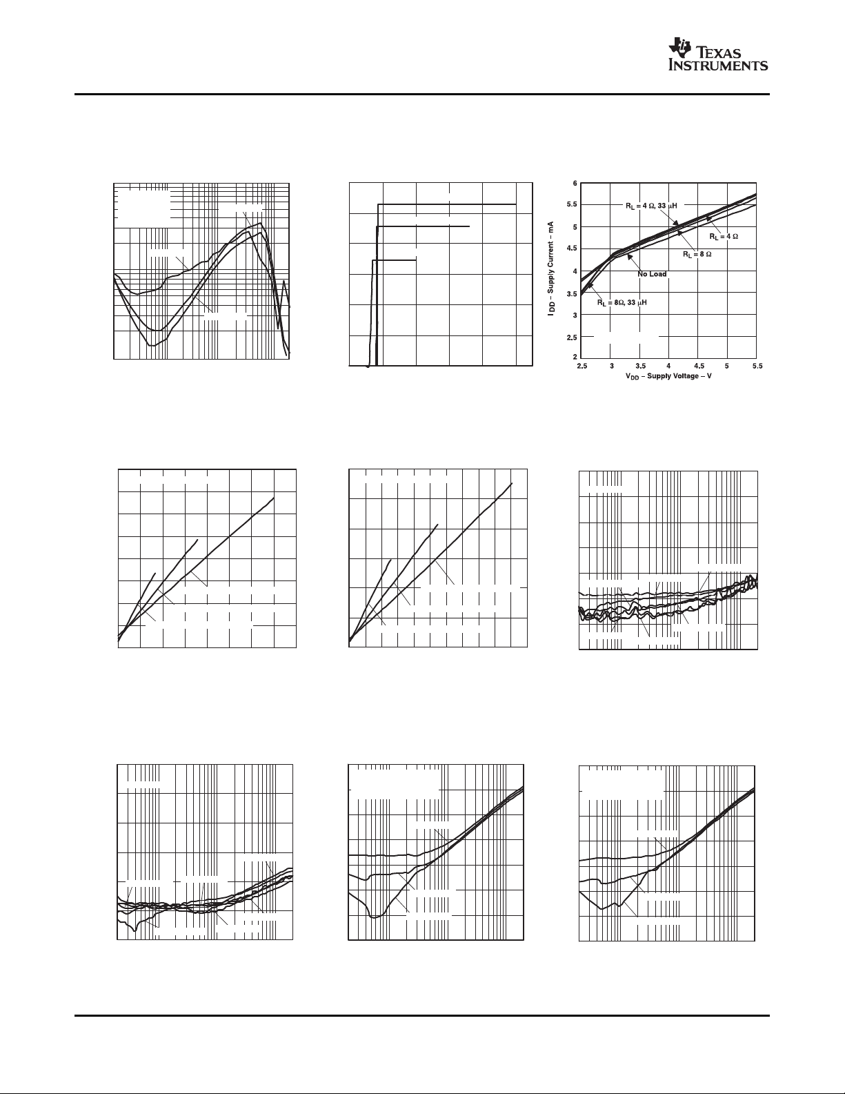
TYPICAL CHARACTERISTICS (continued)
TOTAL HARMONIC DISTORTION SUPPLY CURRENT SUPPLY CURRENT
vs vs vs
FREQUENCY SHUTDOWN VOLTAGE SUPPLY VOLTAGE
Figure 10. Figure 11. Figure 12.
SUPPLY CURRENT SUPPLY CURRENT CROSSTALK
vs vs vs
OUTPUT POWER OUTPUT POWER FREQUENCY
8
Figure 13. Figure 14. Figure 15.
POWER SUPPLY POWER SUPPLY
CROSSTALK REJECTION RATIO REJECTION RATIO
vs vs vs
FREQUENCY FREQUENCY FREQUENCY
Figure 16. Figure 17. Figure 18.
Submit Documentation Feedback

www.ti.com
−75
−70
−65
−60
−55
−50
100 1 k 10 k
VDD = 2.5 V
VDD = 3.6 V
VDD = 5 V
CMRR − Common-Mode Rejection Ratio − dB
f − Frequency − Hz
VIC = 1 VPP,
RL = 8 W,
AV = 6 dB
20 k20
CMRR − Common-Mode Rejection Ratio − dB
−100
−80
−60
−40
−20
0
20
0 1 2 3 4 5
V
ICR
− Common-Mode Input Voltage Range − V
VDD = 5.5 V
VDD = 3.6 V
VDD = 2.5 V
t − Time − 2 ms/div
V
DD
200 mV/div
V
OUT
20 mV/div
C1 − High, 3.6 V
C1 − Amp, 512 mV
C1 − Duty, 12%
−160
−140
−120
−100
−80
−60
−40
−20
0
0 500 1000 1500 2000 2500
−160
−140
−120
−100
−80
−60
−40
−20
0
CI = 1 mF,
Inputs AC Grounded,
AV = 6 dB
VDD = 3.6 V
Input
Output
Supply Signal Ripple − V
Power-Supply Rejection Output − V
f − Frequency − Hz
0
0.1
0.2
0.3
0.4
0.5
0.6
0.7
0 0.2 0.4 0.6 0.8 1 1.2 1.4
Class-AB,
VDD = 3.6 V
RL = 4 Ω
RL = 8 Ω
RL = 4 Ω
RL = 8 Ω
Powers are per Channel
QFN
− Power Dissipation − W
P
D
PO − Output Power − W
Class-AB,
V
DD
= 3.6 V
−90
−80
−70
−60
−50
−40
−30
−20
−10
0
0 0.5 1 1.5 2 2.5 3 3.5 4 4.5 5
DC Common Mode Voltage − V
VDD = 2.7 V
VDD = 5 V
VDD = 3.6 V
RL = 8 W,
VIN = 200 mV
PP
f = 217 Hz
k
SVR
− Supply Voltage Rejection Ratio − dB
SLOS438C – DECEMBER 2004 – REVISED MARCH 2007
TYPICAL CHARACTERISTICS (continued)
COMMOM-MODE
REJECTION RATIO COMMON-MODE GSM POWER
vs REJECTION RATIO SUPPLY REJECTION
COMMON-MODE vs vs
INPUT VOLTAGE FREQUENCY TIME
Figure 19. Figure 20. Figure 21.
TPA2012D2
POWER SUPPLY REJECTION REJECTION RATIO POWER DISSIPATION
SUPLY VOLTAGE
vs vs vs
FREQUENCY DC COMMON-MODE VOLTAGE OUTPUT POWER
Figure 22. Figure 23. Figure 24.
Submit Documentation Feedback
9

www.ti.com
0
10
20
30
40
50
60
70
80
90
100
0 0.5 1 1.5 2 2.5
Efficiency − %
PO − Output Power − W
RL = 4 Ω
VDD = 5 V
VDD = 3.6
V
VDD = 2.5 V
QFN
Class-AB
Powers are per Channel
0
10
20
30
40
50
60
70
80
90
100
0 0.2 0.4 0.6 0.8 1 1.2 1.4
VDD = 5 V
VDD = 3.6 V
VDD = 2.5 V
Class-AB
RL = 8 Ω
Powers are per Channel
QFN
Efficiency − %
PO − Output Power − W
0
0.2
0.4
0.6
0.8
1
1.2
1.4
0 0.5 1 1.5 2 2.5
Class-AB, VDD = 5 V
RL = 4 Ω
RL = 4 Ω
RL = 8 Ω
Powers are per Channel
QFN
− Power Dissipation − W
P
D
PO − Output Power − W
Class-AB, VDD = 5 V
RL = 8 Ω
0
0.1
0.2
0.3
0.4
0.5
0.6
0.7
0 0.2 0.4 0.6 0.8 1 1.2 1.4
Class-AB, VDD = 3.6 V
RL = 4 Ω
RL = 8 Ω
R
L =
4 Ω
RL = 8 Ω
Powers are per Channel
WCSP
− Power Dissipation − W
P
D
PO − Output Power − W
Class-AB,
V
DD
= 3.6 V
0
0.2
0.4
0.6
0.8
1
1.2
1.4
0 0.5 1 1.5 2 2.5
Class-AB, VDD = 5 V
RL = 4 Ω
RL = 4 Ω
RL = 8 Ω
Powers are per Channel
WCSP
− Power Dissipation − W
P
D
PO − Output Power − W
RL = 8 Ω
Class-AB, VDD = 5 V
0
10
20
30
40
50
60
70
80
90
100
0 0.2 0.4 0.6 0.8 1 1.2 1.4 1.6
VDD = 5 V
RL = 4 Ω
VDD = 3.6 V
Class-AB, VDD = 5 V
WCSP
Efficiency − %
PO − Output Power − W
0
10
20
30
40
50
60
70
80
90
100
0 0.2 0.4 0.6 0.8 1 1.2 1.4
VDD = 5 V
RL = 8 Ω
VDD = 3.6 V
Class-AB, VDD = 5 V
WCSP
Efficiency − %
PO − Output Power − W
0
0.2
0.4
0.6
0.8
1
1.2
1.4
1.6
1.8
2
2.5 3 3.5 4 4.5 5
P
O
− Output Power − W
VDD − Supply Voltage − V
RL = 4 W,
THD+N = 10%
RL = 4 W,
THD+N = 1%
RL = 8 W,
THD+N = 10%
RL = 8 W,
THD+N = 1%
TPA2012D2
SLOS438C – DECEMBER 2004 – REVISED MARCH 2007
TYPICAL CHARACTERISTICS (continued)
POWER DISSIPATION EFFICIENCY EFFICIENCY
vs vs vs
OUTPUT POWER OUTPUT POWER OUTPUT POWER
Figure 25. Figure 26. Figure 27.
POWER DISSIPATION POWER DISSIPATION EFFICIENCY
vs vs vs
OUTPUT POWER OUTPUT POWER OUTPUT POWER
10
Figure 28. Figure 29. Figure 30.
EFFICIENCY OUTPUT POWER
vs vs
OUTPUT POWER SUPPLY VOLTAGE
Figure 31. Figure 32.
Submit Documentation Feedback

www.ti.com
AV
DD
PVDD*
Shutdown
Control
0.1 mF
SDR
SDL
PGND AGND
INR+
INR−
INL+
INL−
OUTR+
OUTR−
OUTL+
OUTL−
1 nF
0.1 mF
DAC
G0
G1
1 mF
0.1 mF
4.7 mF
* For QFN, an additional capacitor is recomended for the second PVDD pin.
To Battery
1 nF
1 nF
1 nF
0.1 mF
0.1 mF
to Battery
V
DD
OUTR+
GND
INR+
300 k
C
S
300 k
G0
OUTR−
OUTL+
OUTL−
G1
INR−
INL+
INL−
Gain
Adjust
PWM
Gain
Adjust
PWM
H −
Bridge
H −
Bridge
Internal
Oscillator
Bias
Circuitry
Short−Circuit
Protection
Right
Single−Ended
Input
C
I
C
I
SDR
SDL
C
I
C
I
Left
Single−Ended
Input
to Battery
V
DD
OUTR+
GND
INR+
300 k
C
S
300 k
G0
OUTR−
OUTL+
OUTL−
G1
INR−
INL+
INL−
Gain
Adjust
PWM
Gain
Adjust
PWM
H −
Bridge
H −
Bridge
Internal
Oscillator
Bias
Circuitry
Short−Circuit
Protection
Right
Differential
Input
C
I
C
I
Left
Differential
Input
C
I
C
I
SDR
SDL
TPA2012D2
SLOS438C – DECEMBER 2004 – REVISED MARCH 2007
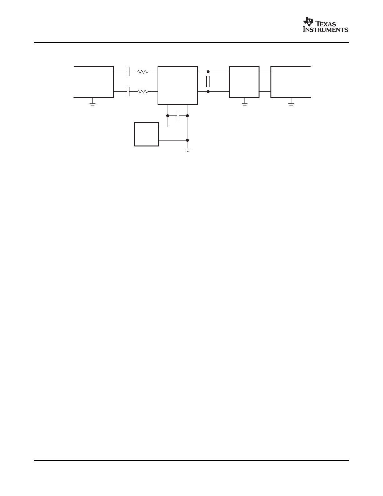
APPLICATION INFORMATION
Figure 34. TPA2012D2 Application Schematic
With Differential Input and Input Capacitors
Figure 33. Typical Application Circuit
Submit Documentation Feedback
Figure 35. TPA2012D2 Application Schematic
With Single-Ended Input
11
www.ti.com
f
c
+
1
ǒ
2p RIC
I
Ǔ
C
I
+
1
ǒ
2p RIf
c
Ǔ
TPA2012D2
SLOS438C – DECEMBER 2004 – REVISED MARCH 2007
Decoupling Capacitor (C
)
S
The TPA2012D2 is a high-performance Class-D audio amplifier that requires adequate power supply decoupling
to ensure the efficiency is high and total harmonic distortion (THD) is low. For higher frequency transients,
spikes, or digital hash on the line a good low equivalent-series-resistance (ESR) ceramic capacitor, typically 1
µ F, placed as close as possible to the device PV
lead works best. Placing this decoupling capacitor close to
DD
the TPA2012D2 is important for the efficiency of the Class-D amplifier, because any resistance or inductance in
the trace between the device and the capacitor can cause a loss in efficiency. For filtering lower-frequency noise
signals, a 4.7 µ F or greater capacitor placed near the audio power amplifier would also help, but it is not
required in most applications because of the high PSRR of this device.
Table 1. Gain Setting
INPUT IMPEDANCE
(k Ω )
Input Capacitors (C
G1 G0 (RI)
0 0 2 6 28.1
0 1 4 12 17.3
1 0 8 18 9.8
1 1 16 24 5.2
)
I
GAIN GAIN
(V/V) (dB)
The TPA2012D2 does not require input coupling capacitors if the design uses a differential source that is biased
from 0.5 V to V
– 0.8 V. If the input signal is not biased within the recommended common-mode input range, if
DD
high pass filtering is needed (see Figure 34 ), or if using a single-ended source (see Figure 35 ), input coupling
capacitors are required.
The input capacitors and input resistors form a high-pass filter with the corner frequency, fc, determined in
Equation 1 .
The value of the input capacitor is important to consider as it directly affects the bass (low frequency)
performance of the circuit. Speakers in wireless phones cannot usually respond well to low frequencies, so the
corner frequency can be set to block low frequencies in this application. Not using input capacitors can increase
output offset.
Equation 2 is used to solve for the input coupling capacitance.
If the corner frequency is within the audio band, the capacitors should have a tolerance of ± 10% or better,
because any mismatch in capacitance causes an impedance mismatch at the corner frequency and below.
(1)
(2)
12
Submit Documentation Feedback
www.ti.com
Copper
Trace Width
Solder Mask
Thickness
Solder
Pad Width
Solder Mask
Opening
Copper Trace
Thickness
TPA2012D2
SLOS438C – DECEMBER 2004 – REVISED MARCH 2007
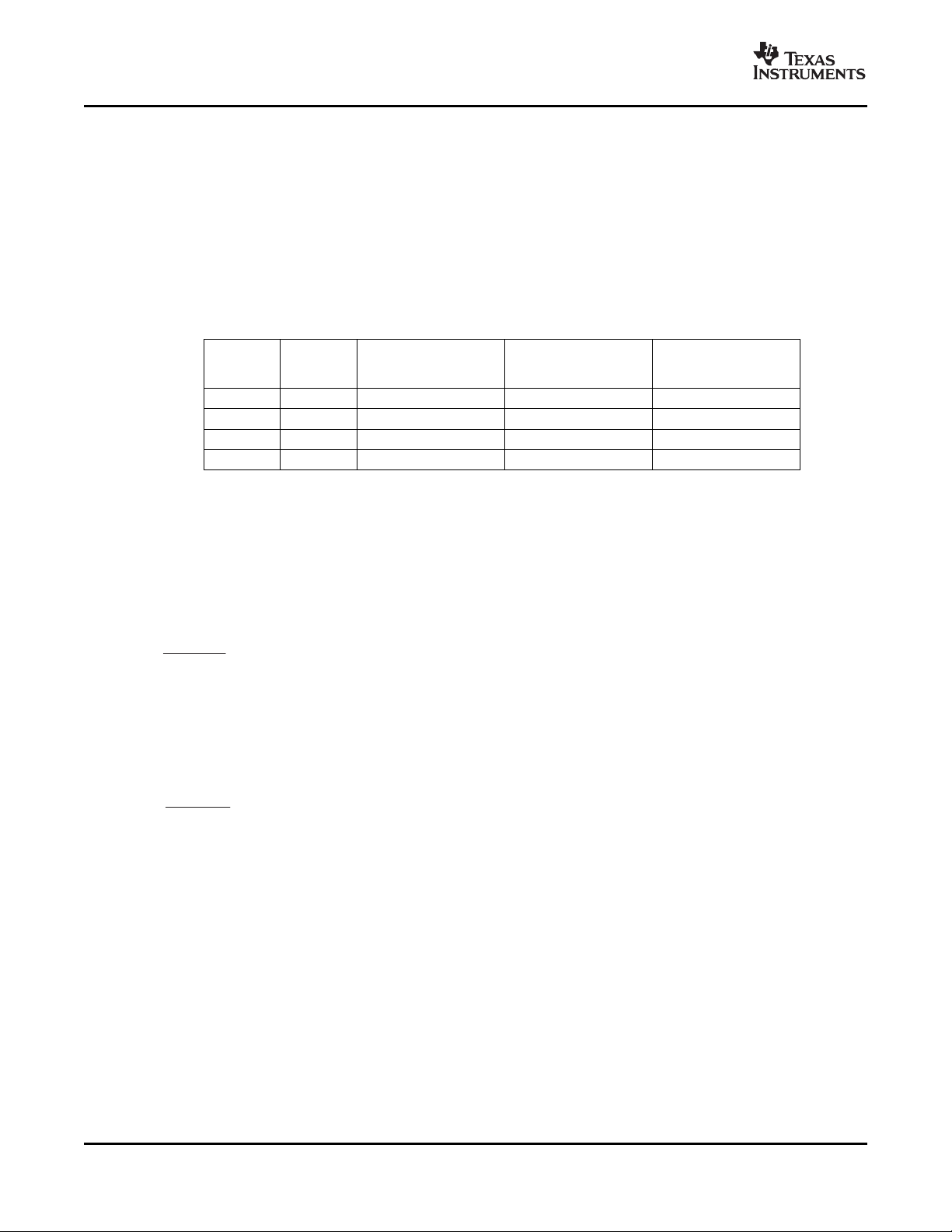
BOARD LAYOUT
In making the pad size for the WCSP balls, it is recommended that the layout use nonsolder mask defined
(NSMD) land. With this method, the solder mask opening is made larger than the desired land area, and the
opening size is defined by the copper pad width. Figure 36 and Table 2 shows the appropriate diameters for a
WCSP layout. The TPA2012D2 evaluation module (EVM) layout is shown in the next section as a layout
example.
Figure 36. Land Pattern Dimensions
Table 2. Land Pattern Dimensions
SOLDER PAD COPPER SOLDER MASK
DEFINITIONS PAD OPENING THICKNESS OPENING THICKNESS
Nonsolder mask 275 µ m 275 µ m x 275 µ m Sq.
defined (NSMD) (+0.0, -25 µ m) (rounded corners)
(1) Circuit traces from NSMD defined PWB lands should be 75 µ m to 100 µ m wide in the exposed area inside the solder mask opening.
Wider trace widths reduce device stand off and impact reliability.
(2) Best reliability results are achieved when the PWB laminate glass transition temperature is above the operating the range of the
intended application.
(3) Recommend solder paste is Type 3 or Type 4.
(4) For a PWB using a Ni/Au surface finish, the gold thickness should be less 0.5 mm to avoid a reduction in thermal fatigue performance.
(5) Solder mask thickness should be less than 20 µ m on top of the copper circuit pattern
(6) Best solder stencil performance is achieved using laser cut stencils with electro polishing. Use of chemically etched stencils results in
inferior solder paste volume control.
(7) Trace routing away from WCSP device should be balanced in X and Y directions to avoid unintentional component movement due to
solder wetting forces.
375 µ m (+0.0, -25 µ m) 1 oz max (32 µ m) 125 µ m thick
(5)
COPPER STENCIL
(1) (2) (3) (4)
(6) (7)
STENCIL
Component Location
Place all the external components very close to the TPA2012D2. Placing the decoupling capacitor, CS, close to
the TPA2012D2 is important for the efficiency of the Class-D amplifier. Any resistance or inductance in the trace
between the device and the capacitor can cause a loss in efficiency.
Submit Documentation Feedback
13

www.ti.com
qJA+
1
Derating Factor
+
1
0.041
+ 24°CńW
TAMax + TJMax * qJAP
Dmax
+ 150 * 24 (1.5) + 114°C
1 nF
Ferrite
Chip Bead
OUTP
OUTN
Ferrite
Chip Bead
1 nF
TPA2012D2
SLOS438C – DECEMBER 2004 – REVISED MARCH 2007
Trace Width
Recommended trace width at the solder balls is 75 µ m to 100 µ m to prevent solder wicking onto wider PCB
traces.
For high current pins (PV
solder balls and at least 500- µ m PCB traces to ensure proper performance and output power for the device.
For the remaining signals of the TPA2012D2, use 75- µ m to 100- µ m trace widths at the solder balls. The audio
input pins (INR+/- and INL+/-) must run side-by-side to maximize common-mode noise cancellation.
EFFICIENCY AND THERMAL INFORMATION
The maximum ambient temperature depends on the heat-sinking ability of the PCB system. The derating factor
for the packages are shown in the dissipation rating table. Converting this to θ
Given θ
dissipation of 1.5W (0.75 W per channel) for 2.1 W per channel, 4- Ω load, 5-V supply, from Figure 25 , the
maximum ambient temperature can be calculated with the following equation.
Equation 4 shows that the calculated maximum ambient temperature is 114 ° C at maximum power dissipation
with a 5-V supply and 4- Ω a load. The TPA2012D2 is designed with thermal protection that turns the device off
when the junction temperature surpasses 150 ° C to prevent damage to the IC. Also, using speakers more
resistive than 4- Ω dramatically increases the thermal performance by reducing the output current and increasing
the efficiency of the amplifier.
of 24 ° C/W, the maximum allowable junction temperature of 150 ° C, and the maximum internal
JA
, PGND, and audio output pins) of the TPA2012D2, use 100- µ m trace widths at the
DD
for the QFN package:
JA
(3)
(4)
OPERATION WITH DACs AND CODECs
In using Class-D amplifiers with CODECs and DACs, sometimes there is an increase in the output noise floor
from the audio amplifier. This occurs when mixing of the output frequencies of the CODEC/DAC mix with the
switching frequencies of the audio amplifier input stage. The noise increase can be solved by placing a low-pass
filter between the CODEC/DAC and audio amplifier. This filters off the high frequencies that cause the problem
and allow proper performance. See Figure 33 for the block diagram.
FILTER FREE OPERATION AND FERRITE BEAD FILTERS
A ferrite bead filter can often be used if the design is failing radiated emissions without an LC filter and the
frequency sensitive circuit is greater than 1 MHz. This filter functions well for circuits that just have to pass FCC
and CE because FCC and CE only test radiated emissions greater than 30 MHz. When choosing a ferrite bead,
choose one with high impedance at high frequencies, and very low impedance at low frequencies. In addition,
select a ferrite bead with adequate current rating to prevent distortion of the output signal.
Use an LC output filter if there are low frequency (< 1 MHz) EMI sensitive circuits and/or there are long leads
from amplifier to speaker.
Figure 37 shows typical ferrite bead and LC output filters.
Figure 37. Typical Ferrite Chip Bead Filter (Chip bead example: TDK: MPZ1608S221A)
14
Submit Documentation Feedback

PACKAGE OPTION ADDENDUM
www.ti.com
5-Feb-2008
PACKAGING INFORMATION
Orderable Device Status
(1)
Package
Type
Package
Drawing
Pins Package
Qty
Eco Plan
TPA2012D2RTJR ACTIVE QFN RTJ 20 3000 Green (RoHS &
no Sb/Br)
TPA2012D2RTJRG4 ACTIVE QFN RTJ 20 3000 Green (RoHS &
no Sb/Br)
TPA2012D2RTJT ACTIVE QFN RTJ 20 250 Green (RoHS &
no Sb/Br)
TPA2012D2RTJTG4 ACTIVE QFN RTJ 20 250 Green (RoHS &
no Sb/Br)
TPA2012D2YZHR ACTIVE DSBGA YZH 16 3000 Green (RoHS &
no Sb/Br)
TPA2012D2YZHT ACTIVE DSBGA YZH 16 250 Green (RoHS &
no Sb/Br)
(1)
The marketing status values are defined as follows:
ACTIVE: Product device recommended for new designs.
LIFEBUY: TI has announced that the device will be discontinued, and a lifetime-buy period is in effect.
NRND: Not recommended for new designs. Device is in production to support existing customers, but TI does not recommend using this part in
a new design.
PREVIEW: Device has been announced but is not in production. Samples may or may not be available.
OBSOLETE: TI has discontinued the production of the device.
(2)
Lead/Ball Finish MSL Peak Temp
CU NIPDAU Level-2-260C-1 YEAR
CU NIPDAU Level-2-260C-1 YEAR
CU NIPDAU Level-2-260C-1 YEAR
CU NIPDAU Level-2-260C-1 YEAR
Call TI Level-1-260C-UNLIM
Call TI Level-1-260C-UNLIM
(3)
(2)
Eco Plan - The planned eco-friendly classification: Pb-Free (RoHS), Pb-Free (RoHS Exempt), or Green (RoHS & no Sb/Br) - please check
http://www.ti.com/productcontent for the latest availability information and additional product content details.
TBD: The Pb-Free/Green conversion plan has not been defined.
Pb-Free (RoHS): TI's terms "Lead-Free" or "Pb-Free" mean semiconductor products that are compatible with the current RoHS requirements
for all 6 substances, including the requirement that lead not exceed 0.1% by weight in homogeneous materials. Where designed to be soldered
at high temperatures, TI Pb-Free products are suitable for use in specified lead-free processes.
Pb-Free (RoHS Exempt): This component has a RoHS exemption for either 1) lead-based flip-chip solder bumps used between the die and
package, or 2) lead-based die adhesive used between the die and leadframe. The component is otherwise considered Pb-Free (RoHS
compatible) as defined above.
Green (RoHS & no Sb/Br): TI defines "Green" to mean Pb-Free (RoHS compatible), and free of Bromine (Br) and Antimony (Sb) based flame
retardants (Br or Sb do not exceed 0.1% by weight in homogeneous material)
(3)
MSL, Peak Temp. -- The Moisture Sensitivity Level rating according to the JEDEC industry standard classifications, and peak solder
temperature.
Important Information and Disclaimer:The information provided on this page represents TI's knowledge and belief as of the date that it is
provided. TI bases its knowledge and belief on information provided by third parties, and makes no representation or warranty as to the
accuracy of such information. Efforts are underway to better integrate information from third parties. TI has taken and continues to take
reasonable steps to provide representative and accurate information but may not have conducted destructive testing or chemical analysis on
incoming materials and chemicals. TI and TI suppliers consider certain information to be proprietary, and thus CAS numbers and other limited
information may not be available for release.
In no event shall TI's liability arising out of such information exceed the total purchase price of the TI part(s) at issue in this document sold by TI
to Customer on an annual basis.
Addendum-Page 1

PACKAGE MATERIALS INFORMATION
www.ti.com
TAPE AND REEL INFORMATION
11-Mar-2008
*All dimensions are nominal
Device Package
TPA2012D2RTJR QFN RTJ 20 3000 330.0 12.4 4.3 4.3 1.5 8.0 12.0 Q2
TPA2012D2RTJT QFN RTJ 20 250 180.0 12.4 4.3 4.3 1.5 8.0 12.0 Q2
TPA2012D2YZHR DSBGA YZH 16 3000 180.0 8.4 2.18 2.18 0.81 4.0 8.0 Q1
TPA2012D2YZHR DSBGA YZH 16 3000 178.0 8.4 2.18 2.18 0.81 4.0 8.0 Q1
TPA2012D2YZHT DSBGA YZH 16 250 178.0 8.4 2.18 2.18 0.81 4.0 8.0 Q1
TPA2012D2YZHT DSBGA YZH 16 250 180.0 8.4 2.18 2.18 0.81 4.0 8.0 Q1
Type
Package
Drawing
Pins SPQ Reel
Diameter
(mm)
Reel
Width
W1 (mm)
A0 (mm) B0 (mm) K0 (mm) P1
(mm)W(mm)
Pin1
Quadrant
Pack Materials-Page 1

PACKAGE MATERIALS INFORMATION
www.ti.com
11-Mar-2008
*All dimensions are nominal
Device Package Type Package Drawing Pins SPQ Length (mm) Width (mm) Height (mm)
TPA2012D2RTJR QFN RTJ 20 3000 346.0 346.0 29.0
TPA2012D2RTJT QFN RTJ 20 250 190.5 212.7 31.8
TPA2012D2YZHR DSBGA YZH 16 3000 190.5 212.7 31.8
TPA2012D2YZHR DSBGA YZH 16 3000 217.0 193.0 35.0
TPA2012D2YZHT DSBGA YZH 16 250 217.0 193.0 35.0
TPA2012D2YZHT DSBGA YZH 16 250 190.5 212.7 31.8
Pack Materials-Page 2


IMPORTANT NOTICE
Texas Instruments Incorporated and its subsidiaries (TI) reserve the right to make corrections, modifications, enhancements, improvements,
and other changes to its products and services at any time and to discontinue any product or service without notice. Customers should
obtain the latest relevant information before placing orders and should verify that such information is current and complete. All products are
sold subject to TI’s terms and conditions of sale supplied at the time of order acknowledgment.
TI warrants performance of its hardware products to the specifications applicable at the time of sale in accordance with TI’s standard
warranty. Testing and other quality control techniques are used to the extent TI deems necessary to support this warranty. Except where
mandated by government requirements, testing of all parameters of each product is not necessarily performed.
TI assumes no liability for applications assistance or customer product design. Customers are responsible for their products and
applications using TI components. To minimize the risks associated with customer products and applications, customers should provide
adequate design and operating safeguards.
TI does not warrant or represent that any license, either express or implied, is granted under any TI patent right, copyright, mask work right,
or other TI intellectual property right relating to any combination, machine, or process in which TI products or services are used. Information
published by TI regarding third-party products or services does not constitute a license from TI to use such products or services or a
warranty or endorsement thereof. Use of such information may require a license from a third party under the patents or other intellectual
property of the third party, or a license from TI under the patents or other intellectual property of TI.
Reproduction of TI information in TI data books or data sheets is permissible only if reproduction is without alteration and is accompanied
by all associated warranties, conditions, limitations, and notices. Reproduction of this information with alteration is an unfair and deceptive
business practice. TI is not responsible or liable for such altered documentation. Information of third parties may be subject to additional
restrictions.
Resale of TI products or services with statements different from or beyond the parameters stated by TI for that product or service voids all
express and any implied warranties for the associated TI product or service and is an unfair and deceptive business practice. TI is not
responsible or liable for any such statements.
TI products are not authorized for use in safety-critical applications (such as life support) where a failure of the TI product would reasonably
be expected to cause severe personal injury or death, unless officers of the parties have executed an agreement specifically governing
such use. Buyers represent that they have all necessary expertise in the safety and regulatory ramifications of their applications, and
acknowledge and agree that they are solely responsible for all legal, regulatory and safety-related requirements concerning their products
and any use of TI products in such safety-critical applications, notwithstanding any applications-related information or support that may be
provided by TI. Further, Buyers must fully indemnify TI and its representatives against any damages arising out of the use of TI products in
such safety-critical applications.
TI products are neither designed nor intended for use in military/aerospace applications or environments unless the TI products are
specifically designated by TI as military-grade or "enhanced plastic." Only products designated by TI as military-grade meet military
specifications. Buyers acknowledge and agree that any such use of TI products which TI has not designated as military-grade is solely at
the Buyer's risk, and that they are solely responsible for compliance with all legal and regulatory requirements in connection with such use.
TI products are neither designed nor intended for use in automotive applications or environments unless the specific TI products are
designated by TI as compliant with ISO/TS 16949 requirements. Buyers acknowledge and agree that, if they use any non-designated
products in automotive applications, TI will not be responsible for any failure to meet such requirements.
Following are URLs where you can obtain information on other Texas Instruments products and application solutions:
Products Applications
Amplifiers amplifier.ti.com Audio www.ti.com/audio
Data Converters dataconverter.ti.com Automotive www.ti.com/automotive
DSP dsp.ti.com Broadband www.ti.com/broadband
Clocks and Timers www.ti.com/clocks Digital Control www.ti.com/digitalcontrol
Interface interface.ti.com Medical www.ti.com/medical
Logic logic.ti.com Military www.ti.com/military
Power Mgmt power.ti.com Optical Networking www.ti.com/opticalnetwork
Microcontrollers microcontroller.ti.com Security www.ti.com/security
RFID www.ti-rfid.com Telephony www.ti.com/telephony
RF/IF and ZigBee® Solutions www.ti.com/lprf Video & Imaging www.ti.com/video
Mailing Address: Texas Instruments, Post Office Box 655303, Dallas, Texas 75265
Copyright © 2008, Texas Instruments Incorporated
Wireless www.ti.com/wireless
 Loading...