

Page 1
www.ti.com
_
+
PWM H-
IN-
Bridge
V
O+
V
O-
Internal
Oscillator
C
S
ToBattery
V
DD
GND
Bias
Circuitry
R
I
R
I
+
-
Differential
Input
TPA2006D1
SHUTDOWN
8
SHUTDOWN
NC
IN+
IN−
V
O−
GND
V
DD
V
O+
8-PINQFN(DRB)PACKAGE
(TOP VIEW)
7
6
5
1
2
3
4
NC − Nointernalconnection
IN+
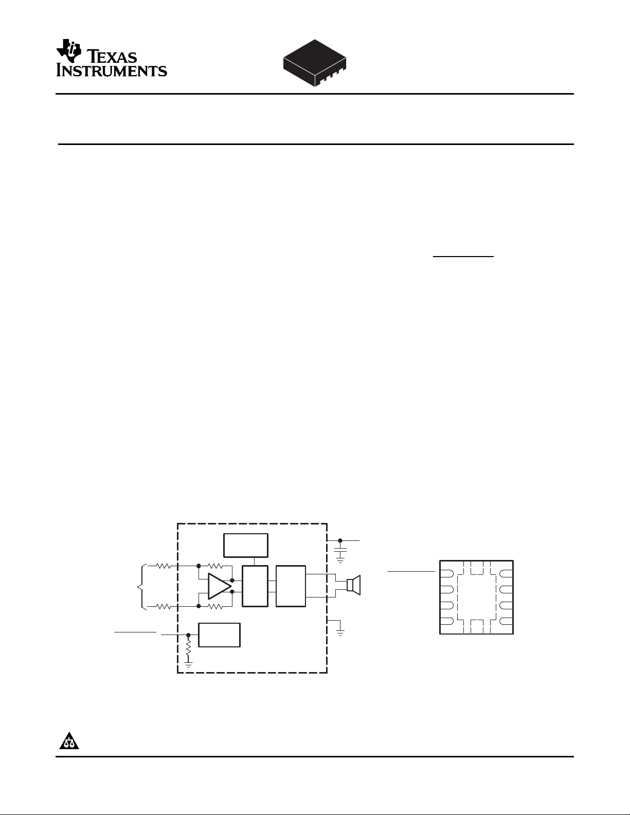
1.45-W MONO FILTER-FREE CLASS-D AUDIO POWER AMPLIFIER WITH 1.8-V
COMPATIBLE INPUT THRESHOLDS
FEATURES APPLICATIONS
• Maximum Battery Life and Minimum Heat
– Efficiency With an 8- Ω Speaker:
• 88% at 400 mW
• 80% at 100 mW
– 2.8-mA Quiescent Current
– 0.5- µ A Shutdown Current
• Shutdown Pin has 1.8-V Compatible
Thresholds
• Only Three External Components
• Optimized PWM Output Stage Eliminates
LC Output Filter
• Internally Generated 250-kHz Switching
Frequency Eliminates Capacitor and
Resistor
• Improved PSRR (–75 dB) and Wide
Supply Voltage (2.5 V to 5.5 V) Eliminates
Need for a Voltage Regulator
• Fully Differential Design Reduces RF
Rectification and Eliminates Bypass
Capacitor
• Improved CMRR Eliminates Two Input
Coupling Capacitors
• Space Saving 3 mm x 3 mm QFN Package
(DRB)
TPA2006D1
SLOS498 – SEPTEMBER 2006
• Ideal for Wireless or Cellular Handsets and
PDAs
DESCRIPTION
The TPA2006D1 is a 1.45-W high efficiency
filter-free class-D audio power amplifier in a 3 mm ×
3 mm QFN package that requires only three external
components. The SHUTDOWN pin is fully
compatible with 1.8-V logic GPIO, such as are used
on low power cellular chipsets.
Features like 88% efficiency, –75-dB PSRR,
improved RF-rectification immunity, and very small
total PCB footprint make the TPA2006D1 ideal for
cellular handsets. A fast start-up time of 1 ms with
minimal pop makes the TPA2006D1 ideal for PDA
applications.
In cellular handsets, the earpiece, speaker phone,
and melody ringer can each be driven by the
TPA2006D1. The TPA2006D1 allows independent
gain while summing signals from separate sources,
and has a low 36 µ V noise floor, A-weighted.
PRODUCTION DATA information is current as of publication date.
Products conform to specifications per the terms of the Texas
Instruments standard warranty. Production processing does not
necessarily include testing of all parameters.
Please be aware that an important notice concerning availability, standard warranty, and use in critical applications of Texas Instruments semiconductor products and disclaimers thereto appears at the end of this data sheet.
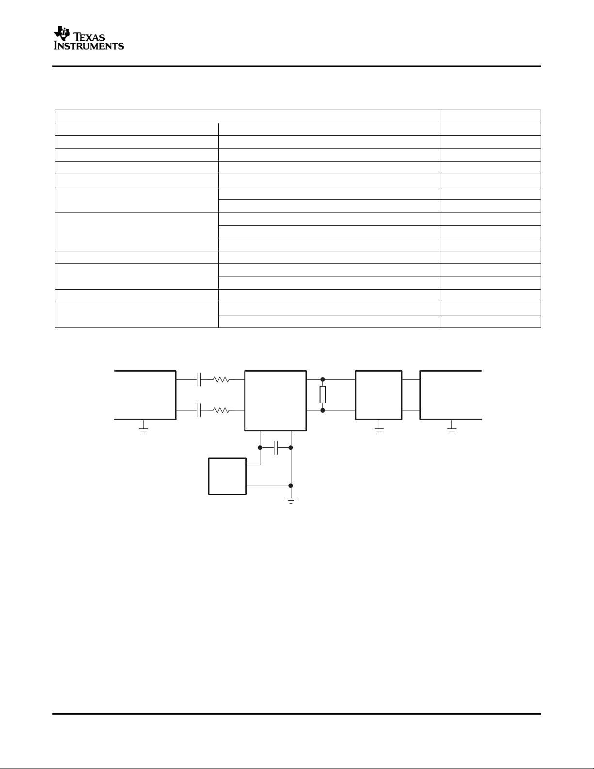
APPLICATION CIRCUIT
Copyright © 2006, Texas Instruments Incorporated
Page 2
www.ti.com
TPA2006D1
SLOS498 – SEPTEMBER 2006
These devices have limited built-in ESD protection. The leads should be shorted together or the device placed in conductive foam
during storage or handling to prevent electrostatic damage to the MOS gates.
ORDERING INFORMATION
T
A
PACKAGE
–40 ° C to 85 ° C 8-pin QFN (DRB) TPA2006D1DRB BTQ
(1) For the most current package and ordering information, see the Package Option Addendum at the end of this document, or see the TI
Web site at www.ti.com .
ABSOLUTE MAXIMUM RATINGS
over operating free-air temperature range unless otherwise noted
V
Supply voltage
DD
V
Input voltage –0.3 V to V
I
Continuous total power dissipation See Dissipation Rating Table
T
Operating free-air temperature –40 ° C to 85 ° C
A
T
Operating junction temperature –40 ° C to 125 ° C
J
T
Storage temperature –65 ° C to 150 ° C
stg
(1) Stresses beyond those listed under absolute maximum ratings may cause permanent damage to the device. These are stress ratings
only, and functional operation of the device at these or any other conditions beyond those indicated under recommended operating
conditions is not implied. Exposure to absolute-maximum-rated conditions for extended periods may affect device reliability.
(1)
(1)
PART NUMBER SYMBOL
TPA2006D1
In active mode –0.3 V to 6 V
In SHUTDOWN mode –0.3 V to 7 V
+ 0.3 V
DD
RECOMMENDED OPERATING CONDITIONS
MIN NOM MAX UNIT
V
Supply voltage 2.5 5.5 V
DD
V
High-level input voltage SHUTDOWN 1.3 V
IH
V
Low-level input voltage SHUTDOWN 0 0.35 V
IL
R
Input resistor Gain ≤ 20 V/V (26 dB) 15 k Ω
I
V
Common mode input voltage range V
IC
T
Operating free-air temperature –40 85 ° C
A
= 2.5 V, 5.5 V, CMRR ≤ –49 dB 0.5 VDD–0.8 V
DD
PACKAGE DISSIPATION RATINGS
PACKAGE DERATING FACTOR
(1)
DRB 21.8 mW/ ° C 2.7 W 1.7 W 1.4 W
(1) Derating factor measure with High K board.
TA≤ 25 ° C TA= 70 ° C TA= 85 ° C
POWER RATING POWER RATING POWER RATING
V
DD
2
Submit Documentation Feedback
Page 3
www.ti.com
V
V
285 kW
R
I
300 kW
R
I
315 kW
R
I
TPA2006D1
SLOS498 – SEPTEMBER 2006
ELECTRICAL CHARACTERISTICS
TA= 25 ° C (unless otherwise noted)
PARAMETER TEST CONDITIONS MIN TYP MAX UNIT
|V
PSRR Power supply rejection ratio V
CMRR Common mode rejection ratio –68 –49 dB
|IIH| High-level input current V
|IIL| Low-level input current V
I
(Q)
I
(SD)
r
DS(on)
f
(sw)
Output offset voltage
| VI= 0 V, AV= 2 V/V, V
OS
(measured differentially)
= 2.5 V to 5.5 V –75 –55 dB
DD
V
= 2.5 V to 5.5 V, VIC= VDD/2 to 0.5 V,
DD
VIC= VDD/2 to V
= 5.5 V, VI= 5.8 V 100 µ A
DD
= 5.5 V, VI= –0.3 V 5 µ A
DD
V
= 5.5 V, no load 3.4 4.9
DD
Quiescent current V
Shutdown current V
Static drain-source on-state
resistance
Output impedance in SHUTDOWN V
Switching frequency V
= 3.6 V, no load 2.8 mA
DD
V
= 2.5 V, no load 2.2 3.2
DD
( SHUTDOWN)
V
= 2.5 V 770
DD
V
= 3.6 V 590 m Ω
DD
V
= 5.5 V 500
DD
( SHUTDOWN)
= 2.5 V to 5.5 V 200 250 300 kHz
DD
= 2.5 V to 5.5 V 25 mV
DD
–0.8 V
DD
= 0.35 V, V
= 2.5 V to 5.5 V 0.5 2 µ A
DD
= 0.35 V >1 k Ω
Gain V
Resistance from shutdown to GND 300 k Ω
OPERATING CHARACTERISTICS
TA= 25 ° C, Gain = 2 V/V, RL= 8 Ω (unless otherwise noted)
PARAMETER TEST CONDITIONS MIN TYP MAX UNIT
THD + N = 10%, f = 1 kHz, RL= 8 Ω V
P
THD+N V
k
SVR
SNR Signal-to-noise ratio V
V
CMRR Common mode rejection ratio V
Z
I
Output power
O
THD + N = 1%, f = 1 kHz, RL= 8 Ω V
V
= 5 V, PO= 1 W, RL= 8 Ω , f = 1 kHz 0.19%
Total harmonic distortion plus
noise
Supply ripple rejection ratio V
Output voltage noise µ V
n
DD
= 3.6 V, PO= 0.5 W, RL= 8 Ω , f = 1 kHz 0.19%
DD
V
= 2.5 V, PO= 200 mW, RL= 8 Ω , f = 1 kHz 0.20%
DD
V
= 3.6 V, Inputs ac-grounded
DD
with Ci= 2 µ F
= 5 V, PO= 1 W, RL= 8 Ω , A-weighted 97 dB
DD
V
= 3.6 V, f = 20 Hz to 20 kHz,
DD
Inputs ac-grounded with Ci= 2 µ F
= 3.6 V, VIC= 1 V
DD
Input impedance 142 150 158 k Ω
Start-up time from shutdown V
= 3.6 V 1 ms
DD
= 2.5 V to 5.5 V
DD
V
= 5 V 1.45
DD
= 3.6 V 0.73 W
DD
V
= 2.5 V 0.33
DD
V
= 5 V 1.19
DD
= 3.6 V 0.59 W
DD
V
= 2.5 V 0.26
DD
f = 217 Hz,
= 200 –67 dB
(RIPPLE)
mV
PP
No weighting 48
A weighting 36
PP
f = 217 Hz –63 dB
RMS
Submit Documentation Feedback
3
Page 4
www.ti.com
SC
150kW
300kW
150kW
150kW
150kW
TPA2006D1
SLOS498 – SEPTEMBER 2006
Terminal Functions
TERMINAL
NAME DRB
IN– 4 I Negative differential input
IN+ 3 I Positive differential input
V
DD
V
O+
GND 7 O High-current ground
V
O-
SHUTDOWN 1 I Shutdown terminal (active low logic)
NC 2 - No Connect, not connected internal to the device. May be left unconnected
Thermal Pad O Should be soldered to a grounded thermal pad on PCB for best thermal performance
6 I Power supply
5 O Positive BTL output
8 O Negative BTL output
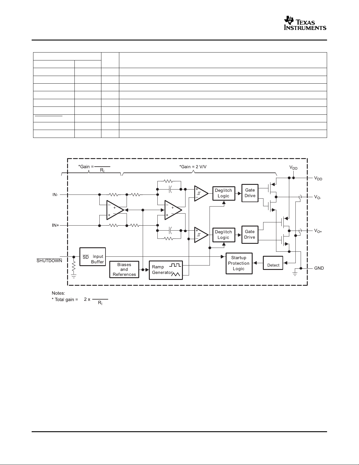
FUNCTIONAL BLOCK DIAGRAM
I/O DESCRIPTION
4
Submit Documentation Feedback
Page 5
www.ti.com
TPA2006D1
IN+
IN-
OUT+
OUT-
V
DD
GND
C
I
C
I
R
I
R
I
Measurement
Output
+
-
1 Fm
+
-
V
DD
Load
30-kHz
Low-Pass
Filter
Measurement
Input
+
-
SLOS498 – SEPTEMBER 2006
TYPICAL CHARACTERISTICS
TABLE OF GRAPHS
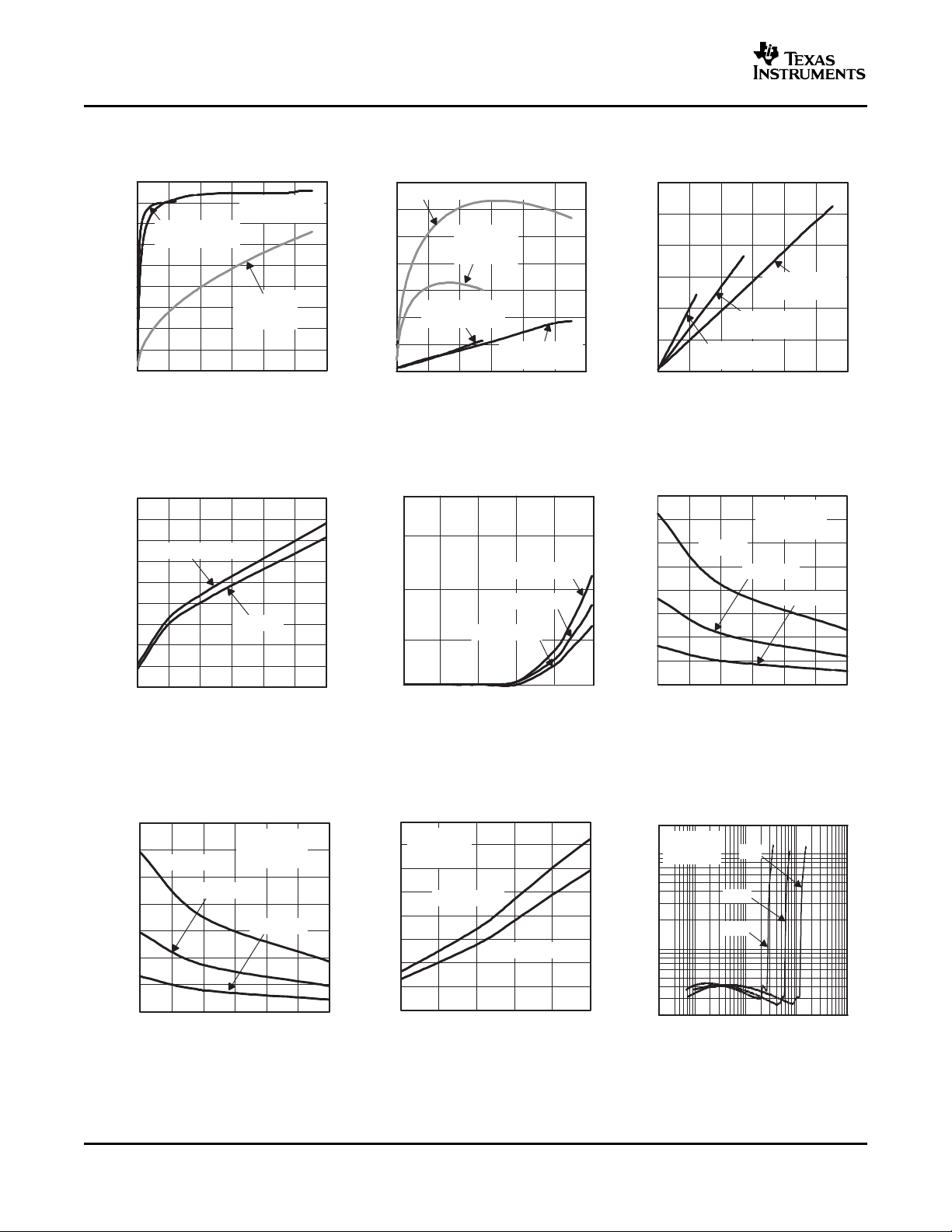
FIGURE
Efficiency vs Output power 1
P
I
(Q)
I
(SD)
P
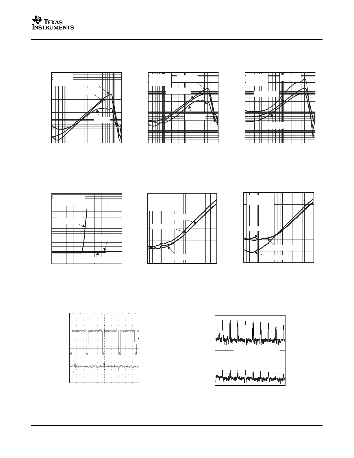
THD+N Total harmonic distortion plus noise vs Frequency 10, 11, 12
K
K
CMRR Common-mode rejection ratio
Power dissipation vs Output power 2
D
Supply current vs Output power 3
Quiescent current vs Supply voltage 4
Shutdown current vs Shutdown voltage 5
Output power
O
vs Supply voltage 8
vs Load resistance 6, 7
vs Output power 9
vs Common-mode input voltage 13
Supply ripple rejection ratio vs Frequency 14, 15
SVR
GSM power supply rejection
Supply ripple rejection ratio vs Common-mode input voltage 18
SVR
vs Time 16
vs Frequency 17
vs Frequency 19
vs Common-mode input voltage 20
TPA2006D1
TEST SET-UP FOR GRAPHS
A. CIis shorted for any common-mode input voltage measurement.
B. A 33- µ H inductor is placed in series with the load resistor to emulate a small speaker for efficiency measurements.
C. The 30-kHz low-pass filter is required even if the analyzer has an internal low-pass filter. An RC low-pass filter
(100 Ω , 47 nF) is used on each output for the data sheet graphs.
Submit Documentation Feedback
5
Page 6
www.ti.com
0
10
20
30
40
50
60
70
80
90
0 0.2 0.4 0.6 0.8 1 1.2
V
DD
L
=2.5V,
R =8 ,33 HW m
Class-AB,
V =5V,
R =8
DD
L
W
P -OutputPower-W
O
Efficiency-%
V
DD
L
=5V,
R =8 ,33 HW m
0
50
100
150
200
250
300
0 0.2 0.4 0.6 0.8 1 1.2
P
O
-OutputPower-W
V =2.5V,
R =8 ,33 H
DD
L
W m
V =3.6V,
R =8 ,33 H
DD
L
W m
V =5V,
R =8 ,33 H
DD
L
W m
SupplyCurrent-mA
0
0.1
0.2
0.3
0.4
0.5
0.6
0.7
0 0.2 0.4 0.6 0.8 1 1.2
P
-
D
PowerDissipation-W
PO-OutputPower-W
Class-AB, V =5V,R =8
DD L
W
Class-AB,
V =3.6V,
R =8
DD
L
W
V =3.6V,
R =8 ,33 H
DD
L
W m
V =5V,
R =8 ,33 H
DD
L
W m
0
0.5
1
1.5
2
0 0.1 0.2 0.3 0.4 0.5
Shutdown Voltage − V
− Shutdown Current −
I
(SD)
Aµ
VDD = 5 V
VDD = 3.6 V
VDD = 2.5 V
0
0.2
0.4
0.6
0.8
1
1.2
1.4
1.6
8 12 16 20 24 28 32
VDD=5V
V =3.6V
DD
V =2.5V
DD
R -LoadResistance-LW
P -OutputPower-W
O
f=1kHz
THD+N=10%
Gain=2V/V
2
2.2
2.4
2.6
2.8
3
3.2
3.4
3.6
3.8
2.5 3 3.5 4 4.5 5 5.5
I
(Q)
− QuiescentCurrent −
mA
V − V
DD
− SupplyVoltage
NoLoad
R =8 ,33 H
L
W m
2.5 3 3.5 4 4.5 5
V -SupplyVDDoltage-V
P -OutputPower-W
O
R =8
f=1kHz
L
W
Gain=2V/V
THD+N=1%
THD+N=10%
0
0.2
0.4
0.6
0.8
1
1.2
1.4
1.6
20
0.1
1
0.001 0.01 1k 10k
PowerOutput − W
THD+N − TotalHarmonicDistortion+Noise − %
0.1k
R =8
f=1kHz
L
W
2.5V
3.6V
5V
10
0
0.2
0.4
0.6
0.8
1
1.2
1.4
8 12 16 20 28
R -LoadResistance-LW
P -OutputPower-W
O
3224
f=1kHz
THD+N=1%
Gain=2V/V
V =2.5V
DD
V =3.6V
DD
VDD=5V
TPA2006D1
SLOS498 – SEPTEMBER 2006
EFFICIENCY POWER DISSIPATION SUPPLY CURRENT
vs vs vs
OUTPUT POWER OUTPUT POWER OUTPUT POWER
Figure 1. Figure 2. Figure 3.
QUIESCENT CURRENT SUPPLY CURRENT OUTPUT POWER
vs vs vs
SUPPLY VOLTAGE SHUTDOWN VOLTAGE LOAD RESISTANCE
Figure 4. Figure 5. Figure 6.
TOTAL HARMONIC DISTORTION +
OUTPUT POWER OUTPUT POWER NOISE
vs vs vs
LOAD RESISTANCE SUPPLY VOLTAGE OUTPUT POWER
6
Figure 7. Figure 8. Figure 9.
Submit Documentation Feedback
Page 7
www.ti.com
10
0.01
0.1
1
20 100 10k 20k
f − Frequency − Hz
THD+N − TotalHarmonicDistortion+Noise − %
P =1W
O
P =0.25W
O
P =0.5W
O
V =5V
DD
R =8LW
1k
10
0.001
0.1
1
20 100 10k 20k
f − Frequency − Hz
THD+N − TotalHarmonicDistortion+Noise − %
0.01
1k
V =3.6V
DD
R =8LW
P =0.25W
O
P =0.5W
O
P =0.125W
O
10
0.001
0.1
1
20 100 10k 20k
f − Frequency − Hz
THD+N − TotalHarmonicDistortion+Noise − %
0.01
1k
V =2.5V
DD
R =8LW
P =0.2W
O
P =0.075W
O
P =0.015W
O
−90
−80
−70
−60
−50
−40
−30
20 100 1k 10k
VDD=5V
VDD=2.5V
f − Frequency − Hz
SopplyRippleRejectionRatio − dB
Inputsfloating
R =8LW
20k
VDD=3.6V
−90
−80
−70
−60
−50
−40
−30
20 100 1k 20k
f − Frequency − Hz
SupplyRippleRejectionRatio − dB
VDD=2.5V
VDD=3.6V
VDD=5V
Inputsac-grounded
C
I
=2 Fm
R
L
=8 W
Gain=2V/V
10k
0.1
1
10
0 0.5 1 1.5 2 2.5
f = 1 kHz
PO = 200 mW
V
IC
− Common Mode Input Voltage − V
THD+N − Total Harmonic Distortion + Noise − %
3 3.5 4 4.5 5
VDD = 2.5 V
VDD = 5 V
VDD = 3.6 V
C1 − High
3.6 V
C1 − Amp
512 mV
C1 − Duty
12%
t − Time − 2 ms/div
V
DD
200 mV/div
V
OUT
20 mV/div
−150
−100
−50
0 400 800 1200 1600 2000
−150
−100
−50
0
0
f − Frequency − Hz
− Output Voltage − dBVV
O
− Supply Voltage − dBVV
DD
VDD Shown in Figure 22
CI = 2 µF,
Inputs ac-grounded
Gain = 2V/V
TPA2006D1
SLOS498 – SEPTEMBER 2006
TOTAL HARMONIC DISTORTION + TOTAL HARMONIC DISTORTION + TOTAL HARMONIC DISTORTION +
NOISE NOISE NOISE
vs vs vs
FREQUENCY FREQUENCY FREQUENCY
Figure 10. Figure 11. Figure 12.
TOTAL HARMONIC DISTORTION +
NOISE SUPPLY RIPPLE REJECTION RATIO SUPPLY RIPPLE REJECTION RATIO
vs vs vs
COMMON MODE INPUT VOLTAGE FREQUENCY FREQUENCY
Figure 13. Figure 14. Figure 15.
GSM POWER SUPPLY REJECTION GSM POWER SUPPLY REJECTION
vs vs
TIME FREQUENCY
Figure 16. Figure 17.
Submit Documentation Feedback
7
Page 8
www.ti.com
−100
−90
−80
−70
−60
−50
−40
−30
−20
−10
0
0 1 2 3 4 5
VIC − Common Mode Input Voltage − V
CMRR − Common Mode Rejection Ratio − dB
VDD = 5 V,
Gain = 2
VDD = 2.5 V
VDD = 3.6 V
−75
−70
−65
−60
−55
−50
20 100 1 k 20 k
VDD = 3.6 V
f − Frequency − Hz
CMRR − Common Mode Rejection Ratio − dB
V
IC
= 200 mV
PP
RL = 8 Ω
Gain = 2 V/V
10 k
−80
−70
−60
−50
−40
−30
−20
−10
0
0 0.5 1 1.5 2 2.5 3 3.5 4 4.5 5
DC Common Mode Voltage − V
Sopply Ripple Rejection Ratio − dB
VDD = 2. 5 V
VDD = 3.6 V
VDD = 5 V
TPA2006D1
SLOS498 – SEPTEMBER 2006
SUPPLY RIPPLE REJECTION RATIO COMMON-MODE REJECTION RATIO COMMON-MODE REJECTION RATIO
vs vs vs
DC COMMON MODE VOLTAGE FREQUENCY COMMON-MODE INPUT VOLTAGE
Figure 18. Figure 19. Figure 20.
8
Submit Documentation Feedback
Page 9

www.ti.com
TPA2006D1
SLOS498 – SEPTEMBER 2006
APPLICATION INFORMATION
FULLY DIFFERENTIAL AMPLIFIER
The TPA2006D1 is a fully differential amplifier with differential inputs and outputs. The fully differential amplifier
consists of a differential amplifier and a common-mode amplifier. The differential amplifier ensures that the
amplifier outputs a differential voltage on the output that is equal to the differential input times the gain. The
common-mode feedback ensures that the common-mode voltage at the output is biased around V
regardless of the common-mode voltage at the input. The fully differential TPA2006D1 can still be used with a
single-ended input; however, the TPA2006D1 should be used with differential inputs when in a noisy
environment, like a wireless handset, to ensure maximum noise rejection.
Advantages of Fully Differential Amplifiers
• Input-coupling capacitors not required:
– The fully differential amplifier allows the inputs to be biased at voltage other than mid-supply. For example,
if a codec has a mid-supply lower than the mid-supply of the TPA2006D1, the common-mode feedback
circuit will adjust, and the TPA2006D1 outputs will still be biased at mid-supply of the TPA2006D1. The
inputs of the TPA2006D1 can be biased from 0.5 V to V
range, input-coupling capacitors are required.
• Mid-supply bypass capacitor, C
(BYPASS)
, not required:
– The fully differential amplifier does not require a bypass capacitor. This is because any shift in the
midsupply affects both positive and negative channels equally and cancels at the differential output.
• Better RF-immunity:
– GSM handsets save power by turning on and shutting off the RF transmitter at a rate of 217 Hz. The
transmitted signal is picked-up on input and output traces. The fully differential amplifier cancels the signal
much better than the typical audio amplifier.
– 0.8 V. If the inputs are biased outside of that
DD
/2
DD
COMPONENT SELECTION
Figure 21 shows the TPA2006D1 typical schematic with differential inputs and Figure 22 shows the TPA2006D1
with differential inputs and input capacitors, and Figure 23 shows the TPA2006D1 with single-ended inputs.
Differential inputs should be used whenever possible because the single-ended inputs are much more
susceptible to noise.
Table 1. Typical Component Values
REF DES VALUE EIA SIZE MANUFACTURER PART NUMBER
R
I
C
S
(1)
C
I
(1) CIis only needed for single-ended input or if V
(with RI= 150 k Ω ) gives a high-pass corner frequency of 321 Hz.
150 k Ω ( ± 0.5%) 0402 Panasonic ERJ2RHD154V
1 µ F (+22%, -80%) 0402 Murata GRP155F50J105Z
3.3 nF ( ± 10%) 0201 Murata GRP033B10J332K
is not between 0.5 V and VDD– 0.8 V. CI= 3.3 nF
ICM
Submit Documentation Feedback
9
Page 10

www.ti.com
Gain +
2 x 150 kW
R
I
ǒ
V
V
Ǔ
f
c
+
1
ǒ
2p RIC
I
Ǔ
C
I
+
1
ǒ
2p RIf
c
Ǔ
TPA2006D1
SLOS498 – SEPTEMBER 2006
Input Resistors (R
The input resistors (R
Resistor matching is very important in fully differential amplifiers. The balance of the output on the reference
voltage depends on matched ratios of the resistors. CMRR, PSRR, and cancellation of the second harmonic
distortion diminish if resistor mismatch occurs. Therefore, it is recommended to use 1% tolerance resistors or
better to keep the performance optimized. Matching is more important than overall tolerance. Resistor arrays
with 1% matching can be used with a tolerance greater than 1%.
Place the input resistors very close to the TPA2006D1 to limit noise injection on the high-impedance nodes.
For optimal performance the gain should be set to 2 V/V or lower. Lower gain allows the TPA2006D1 to operate
at its best, and keeps a high voltage at the input making the inputs less susceptible to noise.
Decoupling Capacitor (C
The TPA2006D1 is a high-performance class-D audio amplifier that requires adequate power supply decoupling
to ensure the efficiency is high and total harmonic distortion (THD) is low. For higher frequency transients,
spikes, or digital hash on the line, a good low equivalent-series-resistance (ESR) ceramic capacitor, typically
1 µ F, placed as close as possible to the device V
the TPA2006D1 is very important for the efficiency of the class-D amplifier, because any resistance or
inductance in the trace between the device and the capacitor can cause a loss in efficiency. For filtering
lower-frequency noise signals, a 10 µ F or greater capacitor placed near the audio power amplifier would also
help, but it is not required in most applications because of the high PSRR of this device.
)
I
) set the gain of the amplifier according to Equation 1 .
I
)
S
lead works best. Placing this decoupling capacitor close to
DD
(1)
Input Capacitors (C
The TPA2006D1 does not require input coupling capacitors if the design uses a differential source that is biased
from 0.5 V to V
common-mode input range, if needing to use the input as a high pass filter (shown in Figure 22 ), or if using a
single-ended source (shown in Figure 23 ), input coupling capacitors are required.
The input capacitors and input resistors form a high-pass filter with the corner frequency, fc, determined in
Equation 2 .
The value of the input capacitor is important to consider as it directly affects the bass (low frequency)
performance of the circuit. Speakers in wireless phones cannot usually respond well to low frequencies, so the
corner frequency can be set to block low frequencies in this application.
Equation 3 is reconfigured to solve for the input coupling capacitance.
If the corner frequency is within the audio band, the capacitors should have a tolerance of ± 10% or better,
because any mismatch in capacitance causes an impedance mismatch at the corner frequency and below.
For a flat low-frequency response, use large input coupling capacitors (1 µ F). However, in a GSM phone the
ground signal is fluctuating at 217 Hz, but the signal from the codec does not have the same 217-Hz fluctuation.
The difference between the two signals is amplified, sent to the speaker, and heard as a 217-Hz hum.
)
I
– 0.8 V (shown in Figure 21 ). If the input signal is not biased within the recommended
DD
(2)
(3)
10
Submit Documentation Feedback
Page 11

www.ti.com
_
+
IN-
IN+
PWM H-
Bridge
V
O+
V
O-
Internal
Oscillator
C
S
ToBattery
V
DD
GND
Bias
Circuitry
R
I
R
I
Differential
Input
TPA2006D1
Filter-FreeClassD
SHUTDOWN
_
+
IN-
IN+
PWM H-
Bridge
V
O+
V
O-
Internal
Oscillator
C
S
ToBattery
V
DD
GND
Bias
Circuitry
R
I
R
I
Differential
Input
TPA2006D1
Filter-FreeClassD
SHUTDOWN
C
I
C
I
TPA2006D1
Filter-FreeClassD
SHUTDOWN
SLOS498 – SEPTEMBER 2006
Figure 21. Typical TPA2006D1 Application Schematic With Differential Input for a Wireless Phone
TPA2006D1
Figure 22. TPA2006D1 Application Schematic With Differential Input and Input Capacitors
Figure 23. TPA2006D1 Application Schematic With Single-Ended Input
Submit Documentation Feedback
11
Page 12

www.ti.com
Gain 1 +
V
O
V
I1
+
2 x 150 kW
R
I1
ǒ
V
V
Ǔ
Gain 2 +
V
O
V
I2
+
2 x 150 kW
R
I2
ǒ
V
V
Ǔ
Filter-FreeClassD
SHUTDOWN
TPA2006D1
SLOS498 – SEPTEMBER 2006
SUMMING INPUT SIGNALS WITH THE TPA2006D1
Most wireless phones or PDAs need to sum signals at the audio power amplifier or just have two signal sources
that need separate gain. The TPA2006D1 makes it easy to sum signals or use separate signal sources with
different gains. Many phones now use the same speaker for the earpiece and ringer, where the wireless phone
would require a much lower gain for the phone earpiece than for the ringer. PDAs and phones that have stereo
headphones require summing of the right and left channels to output the stereo signal to the mono speaker.
Summing Two Differential Input Signals
Two extra resistors are needed for summing differential signals (a total of 5 components). The gain for each
input source can be set independently (see Equation 4 and Equation 5 , and Figure 24 ).
If summing left and right inputs with a gain of 1 V/V, use R
= R
I1
= 300 k Ω .
I2
(4)
(5)
Figure 24. Application Schematic With TPA2006D1 Summing Two Differential Inputs
12
Submit Documentation Feedback
Page 13

www.ti.com
Gain 1 +
V
O
V
I1
+
2 x 150 kW
R
I1
ǒ
V
V
Ǔ
Gain 2 +
V
O
V
I2
+
2 x 150 kW
R
I2
ǒ
V
V
Ǔ
C
I2
+
1
ǒ
2p RI2f
c2
Ǔ
C
I2
u
1
ǒ
2p 150kW 20Hz
Ǔ
C >53nF
I2
_
+
IN-
IN+
PWM H-
Bridge
V
O+
V
O-
Internal
Oscillator
C
S
To Battery
V
DD
GND
Bias
Circuitry
R
I2
R
I2
Differential
Input 1
Filter-Free Class D
SHUTDOWN
R
I1
R
I1
Single-Ended
Input 2
C
I2
C
I2
TPA2006D1
SLOS498 – SEPTEMBER 2006
Summing a Differential Input Signal and a Single-Ended Input Signal
Figure 25 shows how to sum a differential input signal and a single-ended input signal. Ground noise can couple
in through IN+ with this method. It is better to use differential inputs. The corner frequency of the single-ended
input is set by C
driven by a low-impedance source even if the input is not in use
If summing a ring tone and a phone signal, the phone signal should use a differential input signal while the ring
tone might be limited to a single-ended signal.
The high pass corner frequency of the single-ended input is set by CI2. If the desired corner frequency is less
than 20 Hz:
, shown in Equation 8 . To assure that each input is balanced, the single-ended input must be
I2
(6)
(7)
(8)
(9)
(10)
Figure 25. Application Schematic With TPA2006D1 Summing Differential Input and Single-Ended Input
Signals
Submit Documentation Feedback
13
Page 14

www.ti.com
Gain 1 +
V
O
V
I1
+
2 x 150 kW
R
I1
ǒ
V
V
Ǔ
Gain 2 +
V
O
V
I2
+
2 x 150 kW
R
I2
ǒ
V
V
Ǔ
C
I1
+
1
ǒ
2p RI1f
c1
Ǔ
C
I2
+
1
ǒ
2p RI2f
c2
Ǔ
CP+ CI1) C
I2
P
+
RI1 R
I2
ǒ
RI1) R
I2
Ǔ
_
+
IN-
IN+
PWM H-
Bridge
V
O+
V
O-
Internal
Oscillator
C
S
To Battery
V
DD
GND
Bias
Circuitry
R
I2
R
P
Filter-Free Class D
SHUTDOWN
R
I1
Single-Ended
Input 2
C
I2
C
P
Single-Ended
Input 1
C
I1
TPA2006D1
SLOS498 – SEPTEMBER 2006
Summing Two Single-Ended Input Signals
Four resistors and three capacitors are needed for summing single-ended input signals. The gain and corner
frequencies (f
and Figure 26 ). Resistor, RP, and capacitor, CP, are needed on the IN+ terminal to match the impedance on the
IN- terminal. The single-ended inputs must be driven by low impedance sources even if one of the inputs is not
outputting an ac signal.
and fc2) for each input source can be set independently (see Equation 11 through Equation 14 ,
c1
(11)
(12)
(13)
(14)
(15)
Component Location
Place all the external components very close to the TPA2006D1. The input resistors need to be very close to the
TPA2006D1 input pins so noise does not couple on the high impedance nodes between the input resistors and
the input amplifier of the TPA2006D1. Placing the decoupling capacitor, CS, close to the TPA2006D1 is
important for the efficiency of the class-D amplifier. Any resistance or inductance in the trace between the device
and the capacitor can cause a loss in efficiency.
14
Figure 26. Application Schematic With TPA2006D1 Summing Two Single-Ended Inputs
Submit Documentation Feedback
(16)
Page 15

www.ti.com
=
1
Derating Factor
1
0.0218
=45.9 C/W
o
q
JA
=
T
A J JA Dmax
Max= T Max P =125 45.9(0.2)=115.8 C- q -
o
0 V
-5 V
+5 V
Current
OUT+
Differential Voltage
Across Load
OUT-
TPA2006D1
SLOS498 – SEPTEMBER 2006
EFFICIENCY AND THERMAL INFORMATION
The maximum ambient temperature depends on the heat-sinking ability of the PCB system. The derating factor
for the DRB package is shown in the dissipation rating table. Converting this to θJA:
Given θ
dissipation of 0.2 W (Po=1.45 W, 8- Ω load, 5-V supply, from Figure 2 ), the maximum ambient temperature can
be calculated with the following equation.
Equation 18 shows that the calculated maximum ambient temperature is 115.8 ° C at maximum power dissipation
with a 5-V supply and 8- Ω a load, see Figure 2 . The TPA2006D1 is designed with thermal protection that turns
the device off when the junction temperature surpasses 150 ° C to prevent damage to the IC.
ELIMINATING THE OUTPUT FILTER WITH THE TPA2006D1
This section focuses on why the user can eliminate the output filter with the TPA2006D1.
Effect on Audio
The class-D amplifier outputs a pulse-width modulated (PWM) square wave, which is the sum of the switching
waveform and the amplified input audio signal. The human ear acts as a band-pass filter such that only the
frequencies between approximately 20 Hz and 20 kHz are passed. The switching frequency components are
much greater than 20 kHz, so the only signal heard is the amplified input audio signal.
of 45.9 ° C/W, the maximum allowable junction temperature of 125 ° C, and the maximum internal
JA
(17)
(18)
Traditional Class-D Modulation Scheme
The traditional class-D modulation scheme, which is used in the TPA005Dxx family, has a differential output
where each output is 180 degrees out of phase and changes from ground to the supply voltage, V
the differential pre-filtered output varies between positive and negative V
, where filtered 50% duty cycle yields
DD
. Therefore,
DD
0 volts across the load. The traditional class-D modulation scheme with voltage and current waveforms is shown
in Figure 27 . Note that even at an average of 0 volts across the load (50% duty cycle), the current to the load is
high causing a high loss and thus causing a high supply current.
Figure 27. Traditional Class-D Modulation Scheme's Output Voltage and Current Waveforms Into an
Inductive Load With no Input
Submit Documentation Feedback
15
Page 16

www.ti.com
0 V
-5 V
+5 V
Current
OUT+
OUT-
Voltage
Across
Load
0 V
-5 V
+5 V
Current
OUT+
OUT-
Voltage
Across
Load
Output = 0 V
Output > 0 V
TPA2006D1
SLOS498 – SEPTEMBER 2006
TPA2006D1 Modulation Scheme
The TPA2006D1 uses a modulation scheme that still has each output switching from 0 to the supply voltage.
However, OUT+ and OUT- are now in phase with each other with no input. The duty cycle of OUT+ is greater
than 50% and OUT- is less than 50% for positive voltages. The duty cycle of OUT+ is less than 50% and OUTis greater than 50% for negative voltages. The voltage across the load sits at 0 volts throughout most of the
switching period greatly reducing the switching current, which reduces any I2R losses in the load.
Figure 28. The TPA2006D1 Output Voltage and Current Waveforms Into an Inductive Load
Efficiency: Why You Must Use a Filter With the Traditional Class-D Modulation Scheme
The main reason that the traditional class-D amplifier needs an output filter is that the switching waveform
results in maximum current flow. This causes more loss in the load, which causes lower efficiency. The ripple
current is large for the traditional modulation scheme because the ripple current is proportional to voltage
multiplied by the time at that voltage. The differential voltage swing is 2 × V
half the period for the traditional modulation scheme. An ideal LC filter is needed to store the ripple current from
each half cycle for the next half cycle, while any resistance causes power dissipation. The speaker is both
resistive and reactive, whereas an LC filter is almost purely reactive.
The TPA2006D1 modulation scheme has very little loss in the load without a filter because the pulses are very
short and the change in voltage is V
making the ripple current larger. Ripple current could be filtered with an LC filter for increased efficiency, but for
instead of 2 × V
DD
. As the output power increases, the pulses widen
DD
and the time at each voltage is
DD
most applications the filter is not needed.
An LC filter with a cutoff frequency less than the class-D switching frequency allows the switching current to flow
through the filter instead of the load. The filter has less resistance than the speaker that results in less power
dissipated, which increases efficiency.
16
Submit Documentation Feedback
Page 17

www.ti.com
SPKR
+ P
SUP–PSUP THEORETICAL
(at max output power)
SPKR
+
P
SUP
P
OUT
–
P
SUP THEORETICAL
P
OUT
(at max output power)
SPKR
+ P
OUT
ǒ
1
h
MEASURED
*
1
h
THEORETICAL
Ǔ
(at max output power)
hTHEORETICAL +
R
L
RL) 2r
DS(on)
(at max output power)
TPA2006D1
SLOS498 – SEPTEMBER 2006
Effects of Applying a Square Wave Into a Speaker
If the amplitude of a square wave is high enough and the frequency of the square wave is within the bandwidth
of the speaker, a square wave could cause the voice coil to jump out of the air gap and/or scar the voice coil. A
250-kHz switching frequency, however, is not significant because the speaker cone movement is proportional to
2
1/f
for frequencies beyond the audio band. Therefore, the amount of cone movement at the switching frequency
is very small. However, damage could occur to the speaker if the voice coil is not designed to handle the
additional power. To size the speaker for added power, the ripple current dissipated in the load needs to be
calculated by subtracting the theoretical supplied power, P
maximum output power, P
efficiency, η
MEASURED
, minus the theoretical efficiency, η
. The switching power dissipated in the speaker is the inverse of the measured
OUT
SUP THEORETICAL
THEORETICAL
The maximum efficiency of the TPA2006D1 with a 3.6 V supply and an 8- Ω load is 86% from Equation 22 . Using
equation Equation 21 with the efficiency at maximum power (84%), we see that there is an additional 17 mW
dissipated in the speaker. The added power dissipated in the speaker is not an issue as long as it is taken into
account when choosing the speaker.
, from the actual supply power, P
.
SUP
, at
(19)
(20)
(21)
(22)
Submit Documentation Feedback
17
Page 18

www.ti.com
1nF
Ferrite
ChipBead
V
O-
Ferrite
ChipBead
1nF
V
O+
0.1 Fm
33 Hm
33 Hm
V
O-
V
O+
0.1 Fm
0.47 Fm
TPA2006D1
SLOS498 – SEPTEMBER 2006
When to Use an Output Filter
Design the TPA2006D1 without an output filter if the traces from amplifier to speaker are short. The TPA2006D1
passed FCC and CE radiated emissions with no shielding with speaker trace wires 100 mm long or less.
Wireless handsets and PDAs are great applications for class-D without a filter.
A ferrite bead filter can often be used if the design is failing radiated emissions without an LC filter, and the
frequency sensitive circuit is greater than 1 MHz. This is good for circuits that just have to pass FCC and CE
because FCC and CE only test radiated emissions greater than 30 MHz. If choosing a ferrite bead, choose one
with high impedance at high frequencies, but very low impedance at low frequencies.
Use an LC output filter if there are low frequency (< 1 MHz) EMI sensitive circuits and/or there are long leads
from amplifier to speaker.
Figure 29 and Figure 30 show typical ferrite bead and LC output filters.
Figure 29. Typical Ferrite Chip Bead Filter (Chip bead example: NEC/Tokin: N2012ZPS121)
Figure 30. Typical LC Output Filter, Cutoff Frequency of 27 kHz
18
Submit Documentation Feedback
Page 19

PACKAGE OPTION ADDENDUM
www.ti.com
2-Oct-2006
PACKAGING INFORMATION
Orderable Device Status
(1)
Package
Type
Package
Drawing
Pins Package
Qty
Eco Plan
TPA2006D1DRBR ACTIVE SON DRB 8 3000 Green (RoHS &
no Sb/Br)
TPA2006D1DRBRG4 ACTIVE SON DRB 8 3000 Green (RoHS &
no Sb/Br)
TPA2006D1DRBT ACTIVE SON DRB 8 250 Green (RoHS &
no Sb/Br)
TPA2006D1DRBTG4 ACTIVE SON DRB 8 250 Green (RoHS &
no Sb/Br)
(1)
The marketing status values are defined as follows:
ACTIVE: Product device recommended for new designs.
LIFEBUY: TI has announced that the device will be discontinued, and a lifetime-buy period is in effect.
NRND: Not recommended for new designs. Device is in production to support existing customers, but TI does not recommend using this part in
a new design.
PREVIEW: Device has been announced but is not in production. Samples may or may not be available.
OBSOLETE: TI has discontinued the production of the device.
(2)
Eco Plan - The planned eco-friendly classification: Pb-Free (RoHS), Pb-Free (RoHS Exempt), or Green (RoHS & no Sb/Br) - please check
http://www.ti.com/productcontent for the latest availability information and additional product content details.
TBD: The Pb-Free/Green conversion plan has not been defined.
Pb-Free (RoHS): TI's terms "Lead-Free" or "Pb-Free" mean semiconductor products that are compatible with the current RoHS requirements
for all 6 substances, including the requirement that lead not exceed 0.1% by weight in homogeneous materials. Where designed to be soldered
at high temperatures, TI Pb-Free products are suitable for use in specified lead-free processes.
Pb-Free (RoHS Exempt): This component has a RoHS exemption for either 1) lead-based flip-chip solder bumps used between the die and
package, or 2) lead-based die adhesive used between the die and leadframe. The component is otherwise considered Pb-Free (RoHS
compatible) as defined above.
Green (RoHS & no Sb/Br): TI defines "Green" to mean Pb-Free (RoHS compatible), and free of Bromine (Br) and Antimony (Sb) based flame
retardants (Br or Sb do not exceed 0.1% by weight in homogeneous material)
(2)
Lead/Ball Finish MSL Peak Temp
CU NIPDAU Level-2-260C-1 YEAR
CU NIPDAU Level-2-260C-1 YEAR
CU NIPDAU Level-2-260C-1 YEAR
CU NIPDAU Level-2-260C-1 YEAR
(3)
(3)
MSL, Peak Temp. -- The Moisture Sensitivity Level rating according to the JEDEC industry standard classifications, and peak solder
temperature.
Important Information and Disclaimer:The information provided on this page represents TI's knowledge and belief as of the date that it is
provided. TI bases its knowledge and belief on information provided by third parties, and makes no representation or warranty as to the
accuracy of such information. Efforts are underway to better integrate information from third parties. TI has taken and continues to take
reasonable steps to provide representative and accurate information but may not have conducted destructive testing or chemical analysis on
incoming materials and chemicals. TI and TI suppliers consider certain information to be proprietary, and thus CAS numbers and other limited
information may not be available for release.
In no event shall TI's liability arising out of such information exceed the total purchase price of the TI part(s) at issue in this document sold by TI
to Customer on an annual basis.
Addendum-Page 1
Page 20

PACKAGE MATERIALS INFORMATION
www.ti.com
TAPE AND REEL INFORMATION
11-Mar-2008
*All dimensions are nominal
Device Package
TPA2006D1DRBR SON DRB 8 3000 330.0 12.4 3.3 3.3 1.1 8.0 12.0 Q2
TPA2006D1DRBT SON DRB 8 250 180.0 12.4 3.3 3.3 1.1 8.0 12.0 Q2
Type
Package
Drawing
Pins SPQ Reel
Diameter
(mm)
Reel
Width
W1 (mm)
A0 (mm) B0 (mm) K0 (mm) P1
(mm)W(mm)
Pin1
Quadrant
Pack Materials-Page 1
Page 21

PACKAGE MATERIALS INFORMATION
www.ti.com
11-Mar-2008
*All dimensions are nominal
Device Package Type Package Drawing Pins SPQ Length (mm) Width (mm) Height (mm)
TPA2006D1DRBR SON DRB 8 3000 346.0 346.0 29.0
TPA2006D1DRBT SON DRB 8 250 190.5 212.7 31.8
Pack Materials-Page 2
Page 22

Page 23
Page 24

Page 25

IMPORTANT NOTICE
Texas Instruments Incorporated and its subsidiaries (TI) reserve the right to make corrections, modifications, enhancements, improvements,
and other changes to its products and services at any time and to discontinue any product or service without notice. Customers should
obtain the latest relevant information before placing orders and should verify that such information is current and complete. All products are
sold subject to TI’s terms and conditions of sale supplied at the time of order acknowledgment.
TI warrants performance of its hardware products to the specifications applicable at the time of sale in accordance with TI’s standard
warranty. Testing and other quality control techniques are used to the extent TI deems necessary to support this warranty. Except where
mandated by government requirements, testing of all parameters of each product is not necessarily performed.
TI assumes no liability for applications assistance or customer product design. Customers are responsible for their products and
applications using TI components. To minimize the risks associated with customer products and applications, customers should provide
adequate design and operating safeguards.
TI does not warrant or represent that any license, either express or implied, is granted under any TI patent right, copyright, mask work right,
or other TI intellectual property right relating to any combination, machine, or process in which TI products or services are used. Information
published by TI regarding third-party products or services does not constitute a license from TI to use such products or services or a
warranty or endorsement thereof. Use of such information may require a license from a third party under the patents or other intellectual
property of the third party, or a license from TI under the patents or other intellectual property of TI.
Reproduction of TI information in TI data books or data sheets is permissible only if reproduction is without alteration and is accompanied
by all associated warranties, conditions, limitations, and notices. Reproduction of this information with alteration is an unfair and deceptive
business practice. TI is not responsible or liable for such altered documentation. Information of third parties may be subject to additional
restrictions.
Resale of TI products or services with statements different from or beyond the parameters stated by TI for that product or service voids all
express and any implied warranties for the associated TI product or service and is an unfair and deceptive business practice. TI is not
responsible or liable for any such statements.
TI products are not authorized for use in safety-critical applications (such as life support) where a failure of the TI product would reasonably
be expected to cause severe personal injury or death, unless officers of the parties have executed an agreement specifically governing
such use. Buyers represent that they have all necessary expertise in the safety and regulatory ramifications of their applications, and
acknowledge and agree that they are solely responsible for all legal, regulatory and safety-related requirements concerning their products
and any use of TI products in such safety-critical applications, notwithstanding any applications-related information or support that may be
provided by TI. Further, Buyers must fully indemnify TI and its representatives against any damages arising out of the use of TI products in
such safety-critical applications.
TI products are neither designed nor intended for use in military/aerospace applications or environments unless the TI products are
specifically designated by TI as military-grade or "enhanced plastic." Only products designated by TI as military-grade meet military
specifications. Buyers acknowledge and agree that any such use of TI products which TI has not designated as military-grade is solely at
the Buyer's risk, and that they are solely responsible for compliance with all legal and regulatory requirements in connection with such use.
TI products are neither designed nor intended for use in automotive applications or environments unless the specific TI products are
designated by TI as compliant with ISO/TS 16949 requirements. Buyers acknowledge and agree that, if they use any non-designated
products in automotive applications, TI will not be responsible for any failure to meet such requirements.
Following are URLs where you can obtain information on other Texas Instruments products and application solutions:
Products Applications
Amplifiers amplifier.ti.com Audio www.ti.com/audio
Data Converters dataconverter.ti.com Automotive www.ti.com/automotive
DSP dsp.ti.com Broadband www.ti.com/broadband
Clocks and Timers www.ti.com/clocks Digital Control www.ti.com/digitalcontrol
Interface interface.ti.com Medical www.ti.com/medical
Logic logic.ti.com Military www.ti.com/military
Power Mgmt power.ti.com Optical Networking www.ti.com/opticalnetwork
Microcontrollers microcontroller.ti.com Security www.ti.com/security
RFID www.ti-rfid.com Telephony www.ti.com/telephony
RF/IF and ZigBee® Solutions www.ti.com/lprf Video & Imaging www.ti.com/video
Mailing Address: Texas Instruments, Post Office Box 655303, Dallas, Texas 75265
Copyright © 2008, Texas Instruments Incorporated
Wireless www.ti.com/wireless
 Loading...