

Page 1

APA100
100−W Analog Input Class-D Amplifier
TPA2001D1/TAS5111
User’ s Gu ide
August 2004 Audio Power Amplifiers
SLOU170
Page 2

IMPORTANT NOTICE
Texas Instruments Incorporated and its subsidiaries (TI) reserve the right to make corrections, modifications,
enhancements, improvements, and other changes to its products and services at any time and to discontinue
any product or service without notice. Customers should obtain the latest relevant information before placing
orders and should verify that such information is current and complete. All products are sold subject to TI’s terms
and conditions of sale supplied at the time of order acknowledgment.
TI warrants performance of its hardware products to the specifications applicable at the time of sale in
accordance with TI’s standard warranty. Testing and other quality control techniques are used to the extent TI
deems necessary to support this warranty . Except where mandated by government requirements, testing of all
parameters of each product is not necessarily performed.
TI assumes no liability for applications assistance or customer product design. Customers are responsible for
their products and applications using TI components. To minimize the risks associated with customer products
and applications, customers should provide adequate design and operating safeguards.
TI does not warrant or represent that any license, either express or implied, is granted under any TI patent right,
copyright, mask work right, or other TI intellectual property right relating to any combination, machine, or process
in which TI products or services are used. Information published by TI regarding third-party products or services
does not constitute a license from TI to use such products or services or a warranty or endorsement thereof.
Use of such information may require a license from a third party under the patents or other intellectual property
of the third party, or a license from TI under the patents or other intellectual property of TI.
Reproduction of information in TI data books or data sheets is permissible only if reproduction is without
alteration and is accompanied by all associated warranties, conditions, limitations, and notices. Reproduction
of this information with alteration is an unfair and deceptive business practice. TI is not responsible or liable for
such altered documentation.
Resale of TI products or services with statements different from or beyond the parameters stated by TI for that
product or service voids all express and any implied warranties for the associated TI product or service and
is an unfair and deceptive business practice. TI is not responsible or liable for any such statements.
Following are URLs where you can obtain information on other Texas Instruments products and application
solutions:
Products Applications
Amplifiers amplifier.ti.com Audio www.ti.com/audio
Data Converters dataconverter.ti.com Automotive www.ti.com/automotive
DSP dsp.ti.com Broadband www.ti.com/broadband
Interface interface.ti.com Digital Control www.ti.com/digitalcontrol
Logic logic.ti.com Military www.ti.com/military
Power Mgmt power.ti.com Optical Networking www.ti.com/opticalnetwork
Microcontrollers microcontroller.ti.com Security www.ti.com/security
Telephony www.ti.com/telephony
Video & Imaging www.ti.com/video
Wireless www.ti.com/wireless
Mailing Address: Texas Instruments
Post Office Box 655303 Dallas, Texas 75265
Copyright 2004, Texas Instruments Incorporated
Page 3

About This Manual
Information About Cautions and Warnings
Preface
Read This First
This user’s guide describes the characteristics, operation, and the use of the
APA100 reference design board. It covers all pertinent areas involved to
properly use this reference design board along with the devices that it
supports. The physical PCB layout, schematic diagram, and circuit
descriptions are included.
This reference design demonstrates how to make the TPA2001D1 and
T AS5111 into a 100-W class-D amplifier. The user’s guide discusses how the
TPA2001D1 is used as an analog input class-D modulator. The analog
modulator is input to the TAS5111, which is an H−bridge that effectively
extends the supply range from the TPA2001D1’s 3-V rails to 29.5 V with the
TAS5111. The user’s guide also goes into detail on the external feedback using
the TLV2464A quad operational amplifier to add power supply rejection. The
user’s guide shows the measured audio results including: total harmonic
distortion plus noise (THD+N) versus frequency, THD+N versus output power,
signal-to-noise ratio (SNR), output power versus supply voltage, output power
versus load, and supply rejection ratio versus frequency.
How to Use This Manual
- Chapter 1 — EVM Overview
- Chapter 2 — PCB Design
- Chapter 3 — EVM Operation
- Chapter 4 — Technical Information
- Chapter 5 — Measured Results
Information About Cautions and Warnings
This book may contain cautions and warnings.
This is an example of a caution statement.
A caution statement describes a situation that could potentially
damage your software or equipment.
iii
Page 4

Related Documentation From Texas Instruments
This is an example of a warning statement.
A warning statement describes a situation that could potentially
cause harm to you
.
The information in a caution or a warning is provided for your protection. Read
each caution and warning carefully.
Related Documentation From Texas Instruments
To obtain a copy of any of the following TI documents, call the Texas
Instruments Literature Response Center at (800) 47–8924 or the Product
Information Center (PIC) at (972) 644–5580. When ordering, identify this
manual by its title and literature number. Updated documents can also be
obtained through the TI Web site at www.ti.com
Data Sheets: Literature Number:
TPA2001D1 SLOS338
TAS5111 SLES049
TLV2464A SLOS220
.
FCC Warning
This equipment is intended for use in a laboratory test environment only. It
generates, uses, and can radiate radio frequency energy and has not been
tested for compliance with the limits of computing devices pursuant to subpart
J of part 15 of FCC rules, which are designed to provide reasonable protection
against radio frequency interference. Operation of this equipment in other
environments may cause interference with radio communications, in which
case the user at his own expense will be required to take whatever measures
may be required to correct this interference.
iv
Page 5

Contents
Contents
1 EVM Overview 1-1. . . . . . . . . . . . . . . . . . . . . . . . . . . . . . . . . . . . . . . . . . . . . . . . . . . . . . . . . . . . . . . . . . .
1.1 Features 1-2. . . . . . . . . . . . . . . . . . . . . . . . . . . . . . . . . . . . . . . . . . . . . . . . . . . . . . . . . . . . . . . . . .
1.2 Power Requirements 1-2. . . . . . . . . . . . . . . . . . . . . . . . . . . . . . . . . . . . . . . . . . . . . . . . . . . . . . . .
1.2.1 Supply Voltage 1-2. . . . . . . . . . . . . . . . . . . . . . . . . . . . . . . . . . . . . . . . . . . . . . . . . . . . . .
1.2.2 TPA2001D1 and TLV2464A Supply Voltage (3-V Reference) 1-3. . . . . . . . . . . . . .
1.3 EVM Basic Function/Block Diagram 1-3. . . . . . . . . . . . . . . . . . . . . . . . . . . . . . . . . . . . . . . . . . .
2 PCB Design 2-1. . . . . . . . . . . . . . . . . . . . . . . . . . . . . . . . . . . . . . . . . . . . . . . . . . . . . . . . . . . . . . . . . . . . .
2.1 PCB Layout 2-2. . . . . . . . . . . . . . . . . . . . . . . . . . . . . . . . . . . . . . . . . . . . . . . . . . . . . . . . . . . . . . . .
2.1.1 Split Ground Plane 2-2. . . . . . . . . . . . . . . . . . . . . . . . . . . . . . . . . . . . . . . . . . . . . . . . . .
2.1.2 H-Bridge Layout 2-3. . . . . . . . . . . . . . . . . . . . . . . . . . . . . . . . . . . . . . . . . . . . . . . . . . . . .
2.1.3 Analog Section Layout 2-3. . . . . . . . . . . . . . . . . . . . . . . . . . . . . . . . . . . . . . . . . . . . . . .
2.1.4 PCB Layers 2-4. . . . . . . . . . . . . . . . . . . . . . . . . . . . . . . . . . . . . . . . . . . . . . . . . . . . . . . . .
2.2 Bill of Materials 2-6. . . . . . . . . . . . . . . . . . . . . . . . . . . . . . . . . . . . . . . . . . . . . . . . . . . . . . . . . . . . .
2.3 Schematic 2-7. . . . . . . . . . . . . . . . . . . . . . . . . . . . . . . . . . . . . . . . . . . . . . . . . . . . . . . . . . . . . . . . .
3 EVM Operation 3-1. . . . . . . . . . . . . . . . . . . . . . . . . . . . . . . . . . . . . . . . . . . . . . . . . . . . . . . . . . . . . . . . . .
3.1 Quick Start 3-2. . . . . . . . . . . . . . . . . . . . . . . . . . . . . . . . . . . . . . . . . . . . . . . . . . . . . . . . . . . . . . . . .
3.2 Power−Up/Down Sequence 3-3. . . . . . . . . . . . . . . . . . . . . . . . . . . . . . . . . . . . . . . . . . . . . . . . . .
3.3 Reset Button/Mute 3-3. . . . . . . . . . . . . . . . . . . . . . . . . . . . . . . . . . . . . . . . . . . . . . . . . . . . . . . . . .
3.4 Error Signals 3-3. . . . . . . . . . . . . . . . . . . . . . . . . . . . . . . . . . . . . . . . . . . . . . . . . . . . . . . . . . . . . . .
3.5 Changing the Gain 3-4. . . . . . . . . . . . . . . . . . . . . . . . . . . . . . . . . . . . . . . . . . . . . . . . . . . . . . . . . .
4 Technical Information 4-1. . . . . . . . . . . . . . . . . . . . . . . . . . . . . . . . . . . . . . . . . . . . . . . . . . . . . . . . . . . .
4.1 Feedback System Design 4-2. . . . . . . . . . . . . . . . . . . . . . . . . . . . . . . . . . . . . . . . . . . . . . . . . . . .
4.2 TPA2001D1 (Class-D Modulator) 4-7. . . . . . . . . . . . . . . . . . . . . . . . . . . . . . . . . . . . . . . . . . . . .
4.3 TAS5111 (H-Bridge) 4-9. . . . . . . . . . . . . . . . . . . . . . . . . . . . . . . . . . . . . . . . . . . . . . . . . . . . . . . . .
4.4 TLV2464A (Gain Setting and Feedback) 4-9. . . . . . . . . . . . . . . . . . . . . . . . . . . . . . . . . . . . . . .
4.5 LC Filter 4-10. . . . . . . . . . . . . . . . . . . . . . . . . . . . . . . . . . . . . . . . . . . . . . . . . . . . . . . . . . . . . . . . . .
4.6 Thermal 4-11. . . . . . . . . . . . . . . . . . . . . . . . . . . . . . . . . . . . . . . . . . . . . . . . . . . . . . . . . . . . . . . . . .
5 Measured Results 5-1. . . . . . . . . . . . . . . . . . . . . . . . . . . . . . . . . . . . . . . . . . . . . . . . . . . . . . . . . . . . . . .
5.1 Total Harmonic Distortion + Noise 5-2. . . . . . . . . . . . . . . . . . . . . . . . . . . . . . . . . . . . . . . . . . . . .
5.2 Output Power 5-4. . . . . . . . . . . . . . . . . . . . . . . . . . . . . . . . . . . . . . . . . . . . . . . . . . . . . . . . . . . . . .
5.3 Efficiency 5-5. . . . . . . . . . . . . . . . . . . . . . . . . . . . . . . . . . . . . . . . . . . . . . . . . . . . . . . . . . . . . . . . . .
5.4 Gain and Phase Response 5-6. . . . . . . . . . . . . . . . . . . . . . . . . . . . . . . . . . . . . . . . . . . . . . . . . .
5.5 Signal-to-Noise Ratio (SNR) 5-6. . . . . . . . . . . . . . . . . . . . . . . . . . . . . . . . . . . . . . . . . . . . . . . . .
5.6 Supply Ripple Rejection 5-7. . . . . . . . . . . . . . . . . . . . . . . . . . . . . . . . . . . . . . . . . . . . . . . . . . . . .
v
Page 6

Contents
Figures
1−1 THD+N vs Output Power (a), THD+N vs Frequency (b) 1-2. . . . . . . . . . . . . . . . . . . . . . . . . . . .
1−2 APA100 EVM Block Diagram 1-4. . . . . . . . . . . . . . . . . . . . . . . . . . . . . . . . . . . . . . . . . . . . . . . . . . .
2−1 APA100 Split Plane Top Layout 2-2. . . . . . . . . . . . . . . . . . . . . . . . . . . . . . . . . . . . . . . . . . . . . . . . .
2−2 APA100 Split Plane Bottom Layout 2-3. . . . . . . . . . . . . . . . . . . . . . . . . . . . . . . . . . . . . . . . . . . . . .
2−3 Top Copper and Silkscreen 2-4. . . . . . . . . . . . . . . . . . . . . . . . . . . . . . . . . . . . . . . . . . . . . . . . . . . . .
2−4 Bottom Copper and Silkscreen 2-5. . . . . . . . . . . . . . . . . . . . . . . . . . . . . . . . . . . . . . . . . . . . . . . . . .
2−5 Drill Drawing 2-5. . . . . . . . . . . . . . . . . . . . . . . . . . . . . . . . . . . . . . . . . . . . . . . . . . . . . . . . . . . . . . . . .
3−1 Quick Start Module Map 3-2. . . . . . . . . . . . . . . . . . . . . . . . . . . . . . . . . . . . . . . . . . . . . . . . . . . . . . .
4−1 APA100 Block Diagram 4-2. . . . . . . . . . . . . . . . . . . . . . . . . . . . . . . . . . . . . . . . . . . . . . . . . . . . . . . .
4−2 Open- and Closed-Loop Frequency Response 4-3. . . . . . . . . . . . . . . . . . . . . . . . . . . . . . . . . . . .
4−3 Open- and Closed-Loop Frequency Response With TPA2001D1 Pole and
4−4 APA100 Integrator Design 4-4. . . . . . . . . . . . . . . . . . . . . . . . . . . . . . . . . . . . . . . . . . . . . . . . . . . . . .
4−5 PSPICE Circuit for Simulating the Feedback 4-6. . . . . . . . . . . . . . . . . . . . . . . . . . . . . . . . . . . . . .
4−6 PSPICE Simulation of Open−Loop Response 4-7. . . . . . . . . . . . . . . . . . . . . . . . . . . . . . . . . . . . .
4−7 TPA2001D1 Block Diagram 4-8. . . . . . . . . . . . . . . . . . . . . . . . . . . . . . . . . . . . . . . . . . . . . . . . . . . .
4−8 TPA2001D1 Inputs and Outputs With 20-kHz Sine Wave 4-8. . . . . . . . . . . . . . . . . . . . . . . . . . .
4−9 APA100 Output Filter 4-10. . . . . . . . . . . . . . . . . . . . . . . . . . . . . . . . . . . . . . . . . . . . . . . . . . . . . . . . .
5−1 APA100 THD+N vs Frequency With 4-W Load 5-2. . . . . . . . . . . . . . . . . . . . . . . . . . . . . . . . . . .
5−2 APA100 THD+N vs Frequency With 8-W Load 5-2. . . . . . . . . . . . . . . . . . . . . . . . . . . . . . . . . . .
5−3 APA100 THD+N vs Output Power With 4-W Load 5-3. . . . . . . . . . . . . . . . . . . . . . . . . . . . . . . . .
5−4 APA100 THD+N vs Output Power With 8-W Load 5-3. . . . . . . . . . . . . . . . . . . . . . . . . . . . . . . . .
5−5 APA100 Output Power vs Supply Voltage With 4-W Load 5-4. . . . . . . . . . . . . . . . . . . . . . . . . .
5−6 APA100 Output Power vs Supply Voltage With 8-W Load 5-4. . . . . . . . . . . . . . . . . . . . . . . . . .
5−7 APA100 Efficiency vs Output Power With 4-W Load 5-5. . . . . . . . . . . . . . . . . . . . . . . . . . . . . . .
5−8 APA100 Gain vs Frequency With 4-W and 8-W Load 5-6. . . . . . . . . . . . . . . . . . . . . . . . . . . .
5−9 APA100 Supply Ripple Rejection Ratio vs Frequency With 8-W Load 5-7. . . . . . . . . . . . . . .
Canceling Zero 4-4. . . . . . . . . . . . . . . . . . . . . . . . . . . . . . . . . . . . . . . . . . . . . . . . . . . . . . . . . . . . . . .
Tables
2−1 Parts List 2-6. . . . . . . . . . . . . . . . . . . . . . . . . . . . . . . . . . . . . . . . . . . . . . . . . . . . . . . . . . . . . . . . . . . .
3−1 TAS5111 Error Decoding 3-3. . . . . . . . . . . . . . . . . . . . . . . . . . . . . . . . . . . . . . . . . . . . . . . . . . . . . . .
4−1 TAS5111 Thermal Table 4-11. . . . . . . . . . . . . . . . . . . . . . . . . . . . . . . . . . . . . . . . . . . . . . . . . . . . . . .
vi
Page 7

Chapter 1
EVM Overview
This reference design demonstrates how to make the TPA2001D1 and the
T AS5111 into a 100-W class-D amplifier. The user’s guide discusses how the
TPA2001D1 is used as an analog input class-D modulator. The analog
modulator is input to the TAS5111, which is an H-bridge that ef fectively extends
the supply range from the TPA2001D1’s 3-V rails to 29.5 V with the TAS5111.
The 18-V to 29.5-V power supply is applied across the power supply banana
plugs J3 and J4. Apply 18 V to 29.5 V to J3 and 0 V (ground) to J4. A simple
zener diode and NPN transistor circuit is used to create the 3-V supply for the
TPA2001D1 and TLV2464A; therefore, the user only needs to apply the
single-supply voltage.
The analog single-ended input is received through the phono jack, J5. The
user should connect the load across the differential output banana jacks, J1
and J2.
Topic Page
1.1 Features 1-2. . . . . . . . . . . . . . . . . . . . . . . . . . . . . . . . . . . . . . . . . . . . . . . . . . . . .
1.2 Power Requirements 1-2. . . . . . . . . . . . . . . . . . . . . . . . . . . . . . . . . . . . . . . . . .
1.3 EVM Basic Function/Block Diagram 1-3. . . . . . . . . . . . . . . . . . . . . . . . . . . .
EVM Overview
1-1
Page 8

Features
1.1 Features
This reference design or evaluation module (EVM) features the TPA2001D1,
TAS5111, and TLV2464A. For simplicity, this EVM is referred to as the APA100
EVM to cover all parts that are supported in this user’s guide. The APA100
EVM is an evaluation module designed for a quick and easy way to evaluate
the functionality and performance of the 100−W analog input class−D
amplifier.
The features of this amplifier follow.
- Wide supply range of 18 V to 29.5 V
- >85% efficiency into 4 Ω and 8 Ω
- 100 W at 4% THD+N with 29.5-V supply and 4-Ω load
- 100 W at 10% THD+N with 28-V supply and 4-Ω load
- 63 W at 10% THD+N with 29.5-V supply and 8-Ω load
- THD+N = 0.04% at 1 W with 29.5-V supply and 4-Ω load
- THD+N = 0.03% at 1 W with 29.5-V supply and 8-Ω load
- SNR = 95 dB
- Supply rejection = 63 dB at 1 kHz
- Internal short circuit and thermal protection
- Onboard 3−V supply for TPA2001D1 and TLV2464A
- Module gain set to 31.4 dB typical and easily adjusted.
Figure 1−1 shows the amplifier’s (a) THD+N vs output power and (b) THD+N
vs frequency with a 4-Ω load, respectively. More graphs are shown in Chapter
5, Measured Results.
Figure 1−1.THD+N vs Output Power (a), THD+N vs Frequency (b)
20
f = 1 kHz,
10
PVDD = 15 V, 18 V,
20 V, 28 V, 29.5 V
5
2
1
0.5
0.2
0.1
0.05
0.02
0.01
THD+N − Total Harmonic Distortion + Noise − %
100 m 500 m 1 5 10 20 50 100 200
PO − Output Power − W
(a) (b)
100
50
20
10
5
2
1
1 W
0.5
0.2
0.1
0.05
0.02
0.01
THD+N − Total Harmonic Distortion + Noise − %
20 50 100 200 1 k 2 k 10 k 20 k
10 W
f − Frequency − Hz
1.2 Power Requirements
The following sections describe the power requirements of this EVM.
40 W
70 W
1.2.1 Supply Voltage
The 18-V to 29.5-V supply (A+) is applied across the power supply banana
plugs J3 and J4. Apply 18 V to 29.5 V to J3 and ground to J4. A zener diode
1-2
Page 9

EVM Basic Function/Block Diagram
and NPN transistor circuit is used to create the 3-V supply for the TPA2001D1
and TLV2464A; therefore, the user only needs to apply the single-supply
voltage. A+ supply is used for powering the TAS5111 and is input for the zener
diode/NPN transistor circuit used to generate the 3-V supply for the
TPA2001D1 and TLV2464A.
To avoid potential damage to the EVM board, make sure that the
correct cables are connected to their respective terminals as
labeled on the EVM board.
Stresses above 29.5-V maximum voltage rating may cause
permanent damage to the TAS5111.
1.2.2 TPA2001D1 and TLV2464A Supply Voltage (3-V Reference)
The 3-V supply is generated by a 3.9-V zener diode, an NPN transistor, and
a few resistors to supply VDD for the TPA2001D1 and TLV2464A. The 3-V
supply voltage goes through a 20-Ω resistor to filter any noise. Test point 3V
is placed after the 20-Ω resistor to allow the user to remove the 20-Ω resistor
and insert an external 3-V supply. If an external supply is inserted, the voltage
needs to be g r e ater than 2.75 V to enable proper operation of the TPA2001D1
and less than 3.6 V to allow proper voltage levels to the inputs of the T AS5111.
When applying an external voltage reference through test point 3V,
ensure that it does not exceed +3.6 V. Otherwise, this can
permanently damage the installed device under test (DUT).
1.3 EVM Basic Function/Block Diagram
The APA100 EVM uses the TPA2001D1 as the analog modulator. The
TAS5111 level shifts the 3-V, peak-to-peak output to the 18-V to 29.5-V,
peak-to-peak output level of the TAS5111 enabling high−power output. The
TLV2464A is used for the input gain stage, to provide a buffered midsupply
voltage (1.5 V) and as feedback. The feedback improves total harmonic
distortion (THD) and gives the amplifier power supply rejection, which allows
the amplifier to have excellent audio performance even with a noisy power
supply. Chapter 4, Technical Information provides more details about the
component selection and feedback. A block diagram of the reference design
is shown in Figure 1−2.
EVM Overview
1-3
Page 10

EVM Basic Function/Block Diagram
Figure 1−2.APA100 EVM Block Diagram
(TLV2464)
Audio Input
Gain
Analog Input
Class-D
Modulator
TPA2001D1
Feedback
and
Integrator
(TLV2464)
H-Bridge
(TAS5111)
Audio
Output
1-4
Page 11

Chapter 2
PCB Design
This chapter gives layout guidelines for the APA100 reference design.
Topic Page
2.1 PCB Layout 2-2. . . . . . . . . . . . . . . . . . . . . . . . . . . . . . . . . . . . . . . . . . . . . . . . . .
2.2 Bill of Materials 2-6. . . . . . . . . . . . . . . . . . . . . . . . . . . . . . . . . . . . . . . . . . . . . . .
2.3 Schematic 2-7. . . . . . . . . . . . . . . . . . . . . . . . . . . . . . . . . . . . . . . . . . . . . . . . . . . .
PCB Design
2-1
Page 12

PCB Layout
2.1 PCB Layout
The critical part of the design lies particularly in the layout process. The EVM
layout should be followed exactly for optimal performance. The main concern
is the placement of components and the proper routing of signals. Place the
bypass/decoupling capacitors as close as possible to the pins; properly
separate the linear and switching signals from each other. Because of its
importance, carefully consider the ground plane in the layout process. A split
ground plane is ideally preferred.
2.1.1 Split Ground Plane
The split plane used in the EVM separates the ground plane for the H−bridge
and a separate plane for everything else. The ground plane plays an important
role in controlling the noise and other effects that contribute to distortion and
noise on the output. To ensure that the return currents are handled properly,
route the appropriate signals only in their respective sections; this means that
the analog traces should only lay directly above or below the analog ground
section and the H-bridge traces in the H-bridge ground section. Minimize the
length of the traces. Figure 2−1 shows the top layer labeled with Analog
Section and H-Bridge Section to demonstrate how the board is split. The
bottom layer is split along the same line, as shown in Figure 2−2.
Figure 2−1.APA100 Split Plane Top Layout
2-2
Page 13

Figure 2−2.APA100 Split Plane Bottom Layout
PCB Layout
2.1.2 H-Bridge Layout
The H-bridge is laid out based on recommendations from the TAS5111 data
sheet and follows the same pattern as the DAVREF100 EVM board.
1) Keep local decoupling and bootstrap capacitors and resistors close to
pins.
J Minimize trace length to C29, and use wide traces.
J Local PVDD decoupling R35, C35, R36, and C36 traces should be as
short and as wide as possible.
2) Use a ground plane.
3) Use trace impedance from bulk decoupling to PVDD pin, making the trace
50 mm long and 1 mm wide, with separate traces for PVDDA and PVDDB
To ensure proper H-bridge layout, measure the TAS5111 output waveforms at
the pins with a short ground lead on the scope probe to PGND. See application
report Voltage Spike Measurement Technique and Specification (SLEA025).
2.1.3 Analog Section Layout
The analog section is carefully laid out to keep the switching currents from the
TAS5111 away from it. The EVM layout followed these general rules.
1) Keep the operational amplifier away from TAS5111 output and power
2) Minimize nodes connected to IN− pin of the TLV2464A. This is the most
traces.
sensitive node of the reference design.
PCB Design
2-3
Page 14

PCB Layout
2.1.4 PCB Layers
3) Use a split ground plane to keep high switching ground currents from the
operational amplifier circuitry.
4) Place decoupling capacitors close to the TLV2464A and TPA2001D1
5) Place RC filter capacitors (C20, C23, and C24) close to the operational
amplifier, with capacitor grounds connecting with a low−impedance path
to the operational amplifier ground pin.
6) Place RC filters (R8, R10, C8, and C11) close to the TPA2001D1, with
capacitor grounds connecting with a low−impedance path to the
TPA2001D1 AGND pin.
7) Place resistor R13 and capacitor C18 close to the TPA2001D1 inputs.
8) Connect the ground side of the TPA2001D1 ROSC, COSC, VDD, and
BYPASS components to TPA2001D1 AGND before connecting to the rest
of the ground plane.
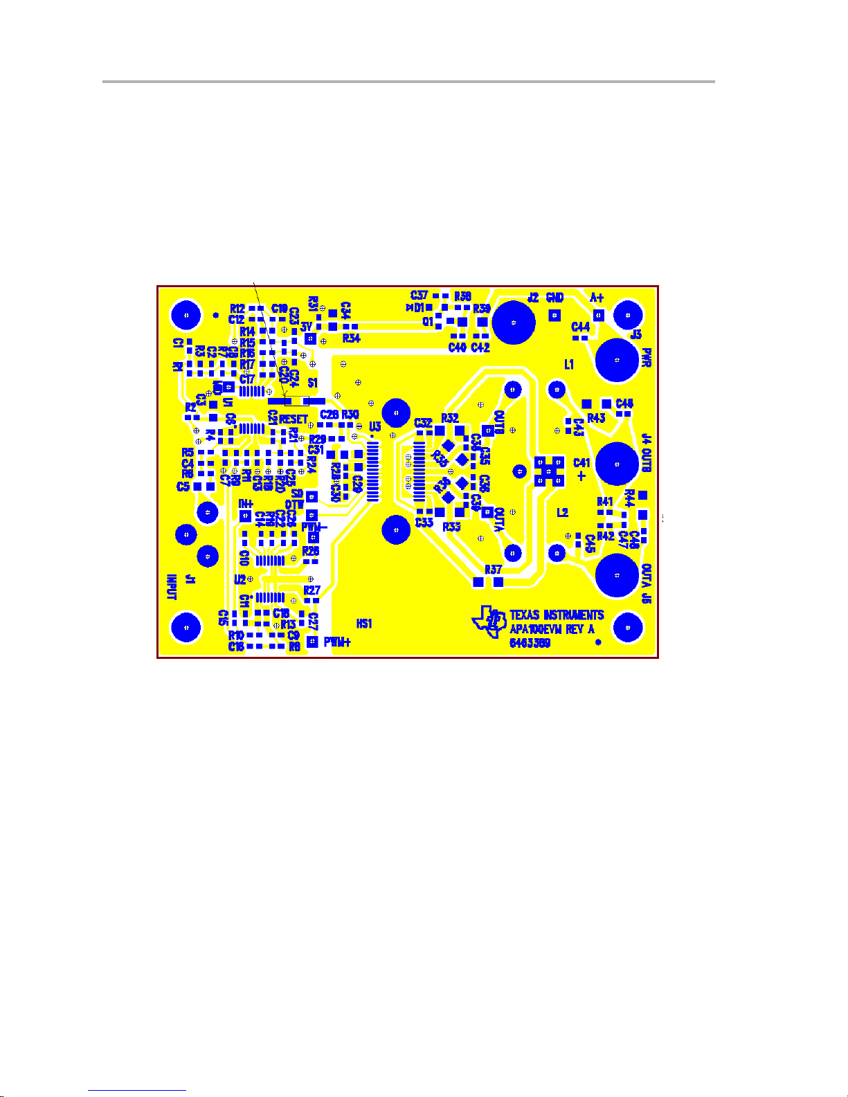
The APA100 EVM board is constructed on a two-layer printed−circuit board
using a copper-clad FR-4 laminate material. The printed−circuit board has a
dimension of 3.4 inch (86,36 mm) X 2.5 inch (63,5 mm), and the board
thickness is 0.062 inch (1,57 mm). Figure 2−3 through NO TAG show the
individual artwork layers.
Figure 2−3.Top Copper and Silkscreen
2-4
Page 15

Figure 2−4.Bottom Copper and Silkscreen
PCB Layout
Figure 2−5.Drill Drawing
3.4 INCH
SIZE QTY STM PLTD
18 4 PLTD
28 40 PLTD
2.5 INCH
42 21 PLTD
89 3 PLTD
116 6 PLTD
140 4 PLTD
PCB Design
2-5
Page 16

Bill of Materials
2.2 Bill of Materials
Table 2−1.Parts List
Reference Qty Value Manufacturer Part Number Description
C23,24 2 22 pF TDK C1608C0G1H220J 50 V, size 603, COG, 5%
C13,19,20,R25 4 56 pF TDK C1608C0G1H560J 50 V, size 603, COG, 5%
C6,9,11,12,14,17,18,
21,49,50
C4,25 2 3300 pF TDK C1608C0G1H332J 50 V, size 603, COG, 5%
C1,30,32,33, 35−37,
40, 42−46,48
C29, 31, 38, 39 2 1 µF TDK 25 V, Size 805, X5R
C2,7,8,10,22,26,27 7 1 µF TDK C1608X5R0J105K 6.3 V, size 603, X5R
C3,5,34 3 10 µF Murata GRM21BR61A106KE19L 10 V, size 805, X5R, 10%
C41 1 1000 µF Panasonic EEUFC1V102 35 V, electrolytic, 20%
C15,C16,R11,R12,
R30
C28, C47 2 DNP
R2,26,27,34 4 20R Yageo 9C06031A20R0JLHFT 1/10W, size 603
R9,28 2 100R Yageo 9C06031A1000JLHFT 1/10W, size 603
R8,10 2 499R Yageo 9C06031A990FKHFT 1/10W, 1%, size 603
R6,14,17,20,24 5 1K Yageo 9C06031A1001JLHFT 1/10W, size 603
R18 1 2K Yageo 9C06031A2001JLHFT 1/10W, size 603
R5,22,23,41,42 6 4.7K Yageo 9C06031A4701FKHFT 1/10W, 1%, size 603
R1,3,4,13,31 5 10K Yageo 9C06031A1002JLHFT 1/10W, size 603
R15,16 2 40.2K Yageo 9C06031A4022FKHFT 1/10W, 1%, size 603
R7,19,29,38 4 120K Yageo 9C06031A1203FKHFT 1/10W, 1%, size 603
R32,33,35,36,43,44 6 1R5 Yageo 9C12063A1R50FKHFT 1/4W, size 1206
R37,39,45,46 4 20R Yageo 9C12063A20R0JLHFT 1/4W, size 1206
R47,48 2 10K Yageo 9C12063A1002FKHFT 1/4W, size 1206
R21 1 DNP
L1, L2 2 22 µH DB Tech DB1320 Inductor, D = 13 mm
D1 1 3.9 V Onsemi MMSZ4686T1 3.9 V zener
D2,3 2 33 V Diodes Inc. SMAJ33A 33 V TVS
S1 1 IPC SM-782 STD PB-SUR-4P Push-button switch
U3 1 Texas Instruments TAS5111 H-bridge, TSSOP32 (DAD)
HS1 1 Heavy MEtal #230 Heatsink #230
U1 1 Texas Instruments TLV2464A SSOP14W
U2 1 Texas Instruments TPA2001D1 SSOP16W
Q1 1 Infineon SMBT3904E6327 NPN, SOT23
J1 1 Phono jack with switch
J2−5 4 Banana + wire
10 220 pF TDK C1608X7R1H221K 50 V, size 603, X7R, 10%
16 0.1 µF TDK C1608X7R1H104K/10 50 V, size 603, X7R
5 0 Ω jumper 0 Ω resistor, size 603
2 Screws 4/40 screws (tightened to
1.5 in × lbs)
Wakefield Wakefield 126 Thermal grease 0.001 inch
thick
2-6
Page 17
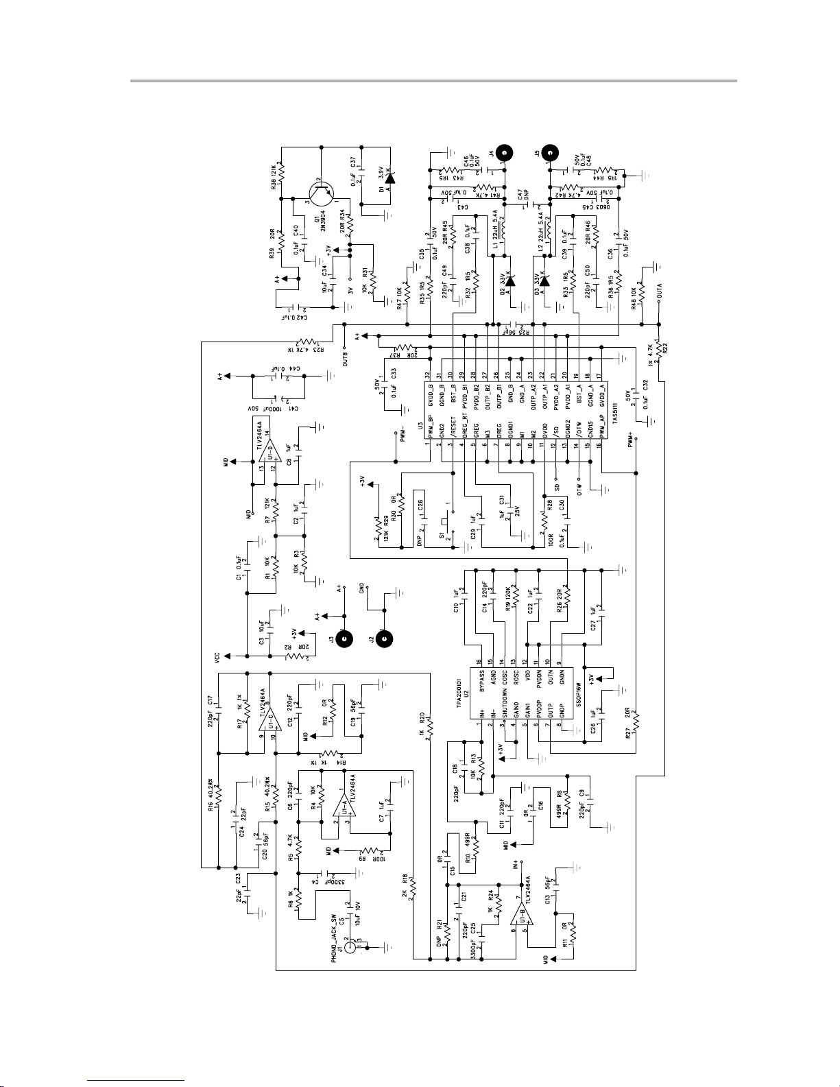
2.3 Schematic
Schematic
PCB Design
2-7
Page 18

2-8
Page 19

Chapter 3
EVM Operation
This chapter covers in detail the operation of the APA100 EVM to guide the
user in evaluating the audio power amplifier and in interfacing the APA100
EVM to an audio input and power supply.
Topic Page
3.1 Quick Start 3-2. . . . . . . . . . . . . . . . . . . . . . . . . . . . . . . . . . . . . . . . . . . . . . . . . . .
3.2 Power−Up/Down Sequence 3-3. . . . . . . . . . . . . . . . . . . . . . . . . . . . . . . . . . . .
3.3 Reset Button/Mute 3-3. . . . . . . . . . . . . . . . . . . . . . . . . . . . . . . . . . . . . . . . . . . .
3.4 Error Signals 3-3. . . . . . . . . . . . . . . . . . . . . . . . . . . . . . . . . . . . . . . . . . . . . . . . .
3.5 Changing the Gain 3-4. . . . . . . . . . . . . . . . . . . . . . . . . . . . . . . . . . . . . . . . . . . .
EVM Operation
3-1
Page 20
Quick Start
3.1 Quick Start
Follow these steps to use the APA100 EVM.
APA100 audio input connection can be made via a phono jack (J1), or by sol-
dering to its pins. The power supply and outputs can be connected with banana
connectors or wires via screw terminals. Figure 3−1 shows numbered callouts
for selected steps.
Figure 3−1.Quick Start Module Map
6
2
5
4
Power Supply
1) Ensure that all external power sources are set to off.
2) Connect an external regulated power supply, set from 18 V to 29.5 V, to
the module A+ (J3) and GND (J4) banana plugs, taking care to observe
marked polarity.
Inputs and Outputs
3) Ensure that the signal source level is set to minimum.
4) Connect the audio source to the input phono connector, J1. The inside of
the phono connector is the audio input, and the outside of the phono connector is ground. Ensure that a single−ended input signal is inserted (NOT
differential or balanced), because the outside of the phono connector is
tied to ground.
5) Connect a 4−Ω or higher impedance speaker to the module OUT+ (J2)
and OUT− (J1) connectors.
3-2
Page 21

Power Up
6) Press and hold the RESET button (S1)
7) Verify correct voltage and input polarity, and set the external power supply
to on.
8) Depress the RESET button (S1).
The EVM begins operation.
9) Adjust the signal source level as needed.
10) Hold RESET button (S1) while powering down
3.2 Power−Up/Down Sequence
The RESET pin of the T AS5111 needs to be held low while turning on power.
This enables the feedback loop to get settled and avoids a loud pop. An RC
filter was placed on the board to help with this, but for optimal pop performance, hold the RESET button (S1) during start-up. The RESET button
should also be held during power-off to reduce power-off pop.
Power−Up/Down Sequence
3.3 Reset Button/Mute
The reset button (S1) controls the RESET pin of the TAS5111. This pin keeps
the outputs of the TAS5111 from switching and can also be used as a mute
button. This is valuable because it allows the feedback loop to stay active and
minimizes the pop going into and coming out of mute.
3.4 Error Signals
The APA100 board has test points to monitor the error signals from the
TAS5111. Test points SD and OTW gives TAS5111 state information as
described in Table 3−1.
Table 3−1.TAS5111 Error Decoding
OTW SD DESCRIPTION
0 0 Overtemperature error ( Tj>150_C )
0 1 Overtemperature warning ( Tj >125_C )
1 0 Overcurrent (>8 A) or undervoltage (GVDD < 7 V) error
1 1 Normal operation, no errors/warnings
EVM Operation
3-3
Page 22

Changing the Gain
3.5 Changing the Gain
The APA100 EVM is set with a gain of 31.4 dB, but can be adjusted. The
front-end has a gain of 4.4 dB (−1.667 V/V), and a back-end gain of 27 dB
(−22.4 V/V), for a total of 31.4 dB (37.3 V/V). The back-end gain needs to be
kept constant, because it is set by the control-loop feedback system with the
TL V2464A, T PA2001D1, and TAS5111. The front-end gain is set by section A
of the quad operational amplifier TLV2464A. The front-end gain is set by
Equation 1, which is a ratio of feedback to input resistors.
Front−end Gain +*
R4
(R5 ) R6)
(VńV)
(1)
The APA100 EVM total gain can then be set by multiplying the front-end and
back-end gains, as shown in Equation 2.
Total Gain + 22.4
R4
(R5 ) R6)
(VńV)
(2)
3-4
Page 23

Chapter 4
Technical Information
This chapter goes into the details of the design of the 100-W amplifier. The
design comprises the modulator, H-bridge, operational amplifier, feedback
loop, LC filter, and thermal.
Topic Page
4.1 Feedback System Design 4-2. . . . . . . . . . . . . . . . . . . . . . . . . . . . . . . . . . . . . .
4.2 TPA2001D1 (Class-D Modulator) 4-7. . . . . . . . . . . . . . . . . . . . . . . . . . . . . . . .
4.3 TAS5111 (H-Bridge) 4-9. . . . . . . . . . . . . . . . . . . . . . . . . . . . . . . . . . . . . . . . . . .
4.4 TLV2464A (Gain Setting and Feedback) 4-9. . . . . . . . . . . . . . . . . . . . . . . . .
4.5 LC Filter 4-10. . . . . . . . . . . . . . . . . . . . . . . . . . . . . . . . . . . . . . . . . . . . . . . . . . . . .
4.6 Thermal 4-11. . . . . . . . . . . . . . . . . . . . . . . . . . . . . . . . . . . . . . . . . . . . . . . . . . . . .
Technical Information
4-1
Page 24
Feedback System Design
4.1 Feedback System Design
The APA100 EVM uses feedback to lower distortion, increase supply ripple
rejection, and make the gain not change with supply voltage. This section goes
through the following steps to close the loop.
1) Take feedback at TAS5111 outputs before the LC filter, so that it is unneccary to cancel two poles of the LC filter.
2) Set corner, Fc, frequency to less than half the minimum switching frequency, Fsw.
3) Add filtering at frequencies greater than 10 times the corner frequency.
4) Add a zero to the integrator to cancel TPA2001D1 pole.
5) Calculate the open−loop gain and set closed−loop gain.
6) Design circuit / component selection.
7) Simulate and adjust.
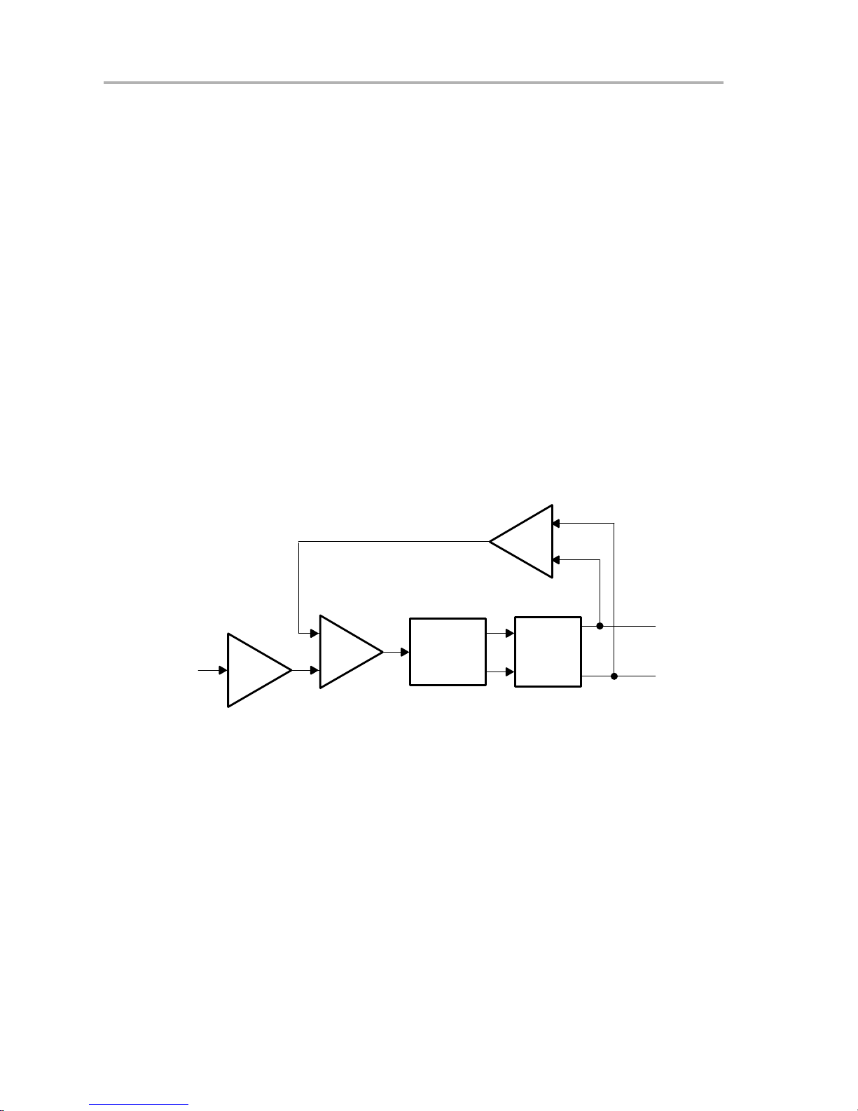
Figure 4−1 shows the block diagram of the feedback loop.
Figure 4−1.APA100 Block Diagram
Sum and
Audio
Output
Gain
The feedback is taken at the TAS5111 outputs before the LC filter. If the
feedback were taken after the LC filter, the two poles caused by the
second−order, low−pass filter would have to be cancelled with zeros in the
integrator. This is difficult and would limit the inductor and capacitor to a tight
tolerance.
When closing the loop, the first thing to choose is the corner frequency . For a
class−D amplifier, the closed−loop corner frequency needs to be less than half
the minimum switching frequency. The minimum switching frequency of the
TPA2001D1 is 200 kHz, limiting the maximum corner frequency to 100 kHz.
Integrate
− 33 dB
Differential to Single -
Ended Converter
Analog Input
Class-D
Modulator
TPA2001D1
Gain = 18 dB Gain = A+/3 V
H-Bridge
(TAS5111)
Audio
Output
An 80-kHz corner frequency was originally designed, but the switching
waveform input to the TPA2001D1 added noise and distortion. Therefore, the
corner frequency was lowered to 40 kHz, and low-pass filters set at 400 kHz
were added in the feedback to reduce the 500-kHz differential signal that is
input to the TPA2001D1. The cutoff frequency of the filter before the
4-2
Page 25
operational amplifier (R22, R23, C20, C23, and C24) was eventually reduced
from 400 kHz to 252 kHz to optimize performance; compensation for this is
discussed later. Notice that in Figure 4−8, the switching frequency of each
output is 250 kHz, but the differential frequency is 500 kHz. The poles greater
than 400−kHz from the low-pass filters do not affect the stability because they
are ten times the corner frequency. The phase from a pole starts at the pole
frequency divided by ten. If the pole is ten times greater than the corner
frequency, the phase margin is not affected.
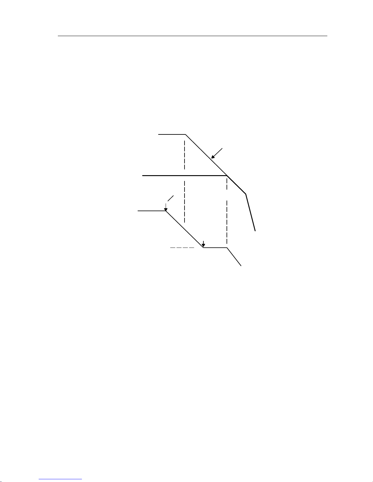
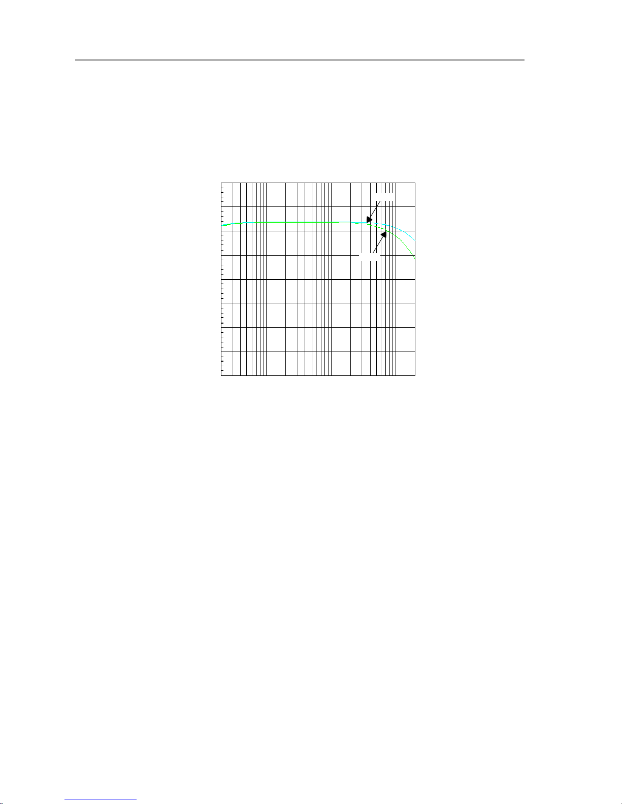
Figure 4−2.Open− and Closed−Loop Frequency Response
10
F
P0
X
20 dB /
Decade
Fc = 40 kHz
Open Loop Gain
Gain − dB
Closed Loop Gain
0 Degrees
F
P0
Feedback System Design
Low Pass
Filters’ Poles
X
X
X
Phase
F
* 10
P0
−90 degrees
Frequency − Hz
Figure 4−2 shows what the open−loop gain and closed−loop gain would look
like if there were no other poles or delays in the system. The integrator pole
causes the open−loop gain to decrease at a rate of 20 dB per decade after the
pole and causes the phase to shift by 90 degrees over a span of two decades
centered at the pole frequency.
Phase Margin + 180° ) Phase (at Fc)
(1)
From Equation 1, the phase margin of this system is 90_. The device needs
0_ to 180_ phase margin for stability, and most designs require 35_ to 180_.
This design would work. However, the TPA2001D1 has an internal feedback
loop with an 80-kHz corner frequency, which adds a pole to the system and
impedes the stability . The added 80-kHz pole drops the phase margin to 45_,
which is still acceptable if there were no other delays.
The added delays decrease phase margin; therefore, more phase margin is
needed to ensure stability. A zero is added to cancel the pole, which returns
the overall closed−loop frequency response back to the original design. The
zero can be created by adding a resistor in series with the integrator feedback
resistor. Figure 4−3 shows the effects of the added zero.
Technical Information
4-3
Page 26

Feedback System Design
Figure 4−3.Open− and Closed−Loop Frequency Response With TPA2001D1 Pole and
Canceling Zero
Open Loop Gain
Gain − dB
Closed Loop Gain
F
P0
X
20 dB /
Decade
Phase
0 Degrees
−90 Degrees
Fc = 40 kHz
F
P0
10
F
* 10
P0
Frequency − Hz
80 kHz
>400 kHz
X
X
X
Now that the poles and zeros have been realized, the closed−loop gain can
be set. First, calculate the open−loop gain by multiplying the gain (adding in
dB) of each block, if there was no feedback. The integrator block adds gain of
the feedback impedance/input resistor at the given frequency. The feedback
impedance is the impedance of C24 + R25 (C21 is overlooked because it has
a large enough impedance to be considered open).
Gain of integrator = Z
+ R25/R18 (Z
C24
= 1/(2π x C24 x f))
C24
The TPA2001D1 has a gain set to 18 dB. The TAS5111 converts the 3-V PWM
to the A+ rail (18 V to 29.5 V). The open−loop gain from the TAS5111 can range
from 18 V/3 V = 6 V/V to 29.5 V/3 V = 9.8 V/V (17 dB to 29 dB). Adding the
gains of each stage in dB:
Open−loop gain = Integrator gain + 18 dB + 17 dB to 20 dB.
Figure 4−4.APA100 Integrator Design
Input
Amplifier
4-4
R18
MID
R21
R24
_
+
C21
R20
C25
− 33 dB
Differential to Single-
Ended Converter
TPA2001D1
+
TAS5111
35 dB
Audio
Output
Page 27

Feedback System Design
The closed−loop gain is set to 27 dB to allow enough gain from the 3−V signal
to the A+ voltage range. This leaves sufficient low−frequency correction.
Figure 4−4 shows the circuit used for the APA100 feedback. Equation (2)
shows the closed−loop response.
Closed−loop gain + 45
Resistors R20 and R18 need to be set low to limit noise. Resistor R18 is set
to 2000 Ω and R18 set to 1000 Ω for a closed−loop gain of 22.4 V/V.
To calculate the values for the other resistors and capacitors, the open−loop
response needs to be examined; so, assume that R20 is not placed. Fix the
gain of the TPA2001D1 + TAS5111 = 3 5 d B = 5 6 V/ V. As Equation (3) shows,
the open−loop gain is the gain of the TPA2001D1 + TAS5111 times the
feedback impedance (Zf) of the integrator circuit/the input resistance (R18).
Open−loop gain + 56
The feedback impedance (Zf) is the impedance of C21 in parallel to the
impedance of C25 plus R24.
Zf +
The feedback impedance can be reduced as shown in Equation 5.
Zf +
1
sC21
s (C21 ) C25
ø
ǒ
sC25
1
1
R20
R18
Zf
R18
) R24
Ǔ
1 ) s R24 C25)
ǒ
1 ) s
R24 C21 C25
C21)C25
(2)
(3)
(4)
Ǔ
(5)
The feedback impedance is substituted into the open−loop gain equation as
shown in Equation 6.
Open−loop gain +
From Equation 6, there are two poles and one zero. The first pole is at dc
from the 1/s term. The first pole actually gets pushed out if R21 is installed,
but it is still a very low frequency. The poles and zeros are shown in Equations 7 and 8.
Fz +
Fp +
To achieve a 40-kHz bandwidth, the open−loop gain (Equation 6) must equal
22.4 V/V (27 dB) at f = 40 kHz (s = −j 2π f).
s R18 (C21 ) C25
2p R24 C25
2p R24 C21 C25
56
1
C21 ) C25
(Hz)
1 ) s R24 C25)
ǒ
1 ) s
(Hz)
R24 C21 C25
C21)C25
Technical Information
(6)
Ǔ
(7)
(8)
4-5
Page 28

Feedback System Design
Instead of calculating the bandwidth, PSPICE was used with a linearized
circuit (see Figure 4−5) to simulate and adjust the component values to
approximately 40-kHz bandwidth. Then, Equations 7 and 8 were used to set
the poles and zeros. The first op amp (U1) in the simulation circuit of
Figure 4−5 is the integrator; the second op amp (U2) sets the 80-kHz pole; the
third (U3) adds the gain from the TPA2001D1 and TAS5111 (56 V/V); and the
final op amp (U4) is the divide−by−45 feedback amplifier.
Figure 4−5.PSPICE Circuit for Simulating the Feedback
R18
1k
4
V2
1.5
0
C10
3
V1
1
0
R121
3
20
U10A
3
+
2
−
R14
2k
R24
1k
Integrator for APA100
411
OUT
0
R21
200k
C21
220p
V+
1
TLV2464A
V−
C25
3.3n
R1
100
VDB
R112
C1
1n
0
U11A
3
3
+
V+
OUT
2
TLV2464A
−
V−
R133
1k
C116
2nF
11
0
R120
10
1k
adds 80kHz pole for TPA2001D1
1
C117
20u
V3
3
0
R119
1k
U12A
3
adds 56V/V of gain from
TPA2001D1 + TAS5111.
Output of this opamp is
simulating output of
TAS5111.
4
3
+
V+
OUT
2
TLV2464A
−
V−
11
0
R115
56k
1
R23
4.7k
U13A
3
3
+
2
R16
−
40k
VDB
55
VP
C24
56p
0
filterdivide by 45 in
feedback of APA100
4
OUT
11
V+
TLV2464A
V−
0
R17
1k
C26
56p
1
C27
22p
First, resistor R18 was removed to give an open−loop response, with the
APA100 output being simulated by the output of the RC filter after the third op
amp. Taking the gain and phase after the RC filter takes into account the
252−kHz filtering before the feedback op amp.
Then, R24 was set low and C25 was adjusted to make the output of the third
op amp equal to the closed−loop gain (27 dB) at 40 kHz; C25 was kept less
than one−tenth of C25. Once the open−loop frequency was approximately 40
kHz, R24 was adjusted to set the zero to 48.2 kHz (needing to stay lower than
the pole of the TPA2001D1). The zero was set much lower than 80 kHz for
compensation, so that the cutof f frequency of the filter before the op amp (R22,
R23, C20, C23, and C24) could be reduced from 400 kHz to 252 kHz. Resistor
R24 was set to 1000 Ω, and capacitor C25 set to 3.3 nF.
The second pole, Fp from Equation 8, was set to 770 kHz by adjusting
capacitor C21 to 220 pF.
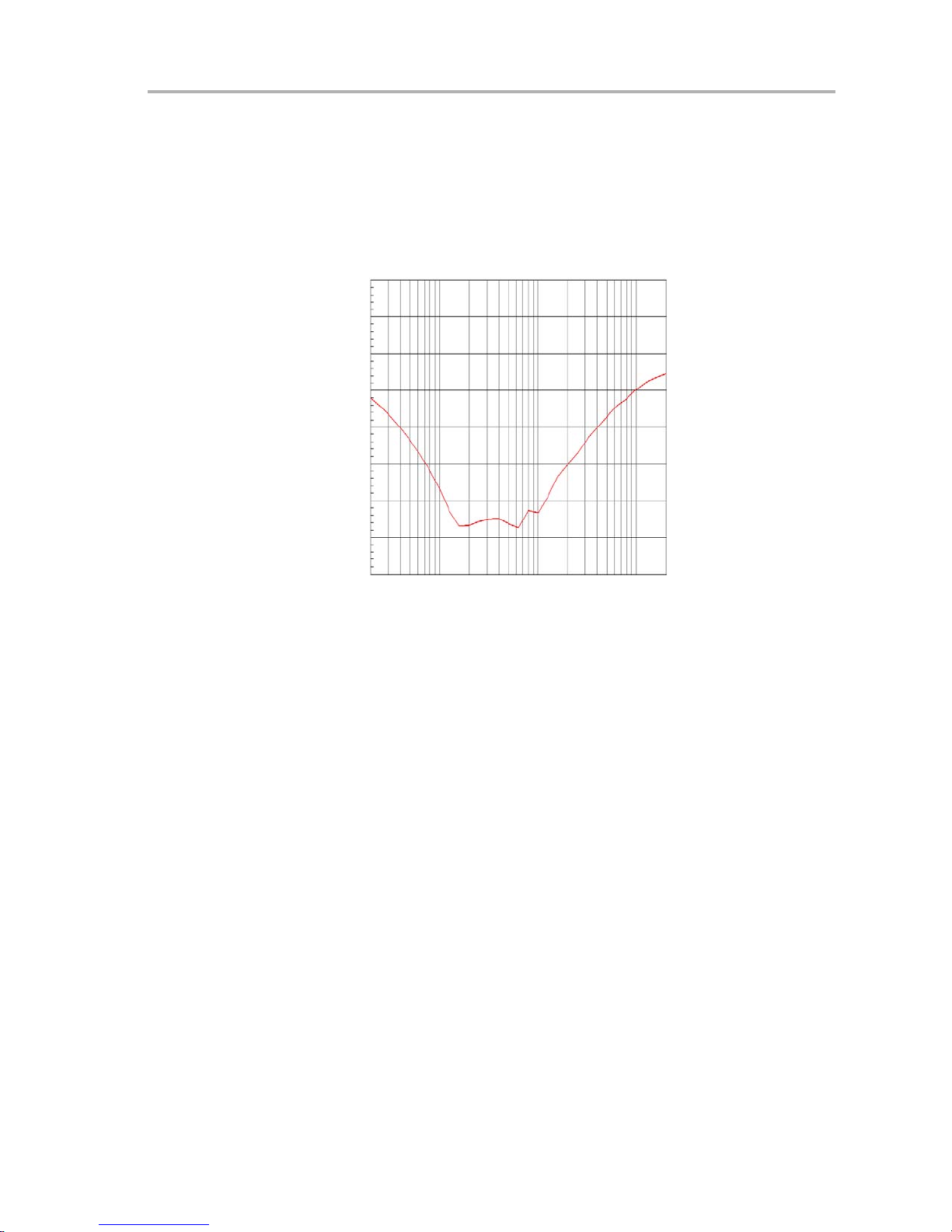
The circuit was simulated to show 40-kHz bandwidth with 49_ phase margin
(see Figure 4−6). The red curve (simulating APA100 output) hits 27 dB at 40
kHz, and at 40-kHz frequency the phase margin (blue curve) is 49_.
The green curve is the output of the integrator. Notice that the green curve’s
slope levels off at 48 kHz, showing that the zero is properly placed. The zero
does not cause the TAS5111 output (red curve) to level off at the zero
frequency because the pole of the TPA2001D1 at 80 kHz keeps the overall
slope constant. The red curves slope increases after 770 kHz due to the
integrator pole from C21.
4-6
Page 29

Figure 4−6.PSPICE Simulation of Open−Loop Response
200
Phase (5)
100
−0
TAS5111
Output (dB)
Integrator
−100
−200
Output (dB)
TPA2001D1 (Class-D Modulator)
−300
100 1 k 10 k
4.2 TPA2001D1 (Class-D Modulator)
The TPA2001D1 was chosen as an excellent performance, low-cost analog
class-D modulator. A class-D modulator takes an analog input signal and
outputs a pulse width modulated (PWM) signal. The TPA2001D1 was selected
over other class-D amplifiers because of the following reasons.
1) Supply voltage range of 2.75 V to 5.5 V (matches up well with TAS5111
H-bridge).
2) Low noise (40 µV rms)
3) Low total harmonic distortion plus noise across 20 Hz to 20 kHz (<0.3%
over 20-Hz to 20-kHz frequency range)
4) Low cost (~$0.75 each in 1 kU)
The TPA2001D1 takes an analog input signal, gains it up, and compares it to
a 250-kHz triangle wave. The output of the comparator is a PWM signal. This
PWM signal is processed to make a differential signal, and it is sent to the
output MOSFETs. The TPA2001D1 outputs are capable of driving 1 W of
output power, but they are only driving high impedance in this case (the
TAS5111 inputs). The TPA2001D1 block diagram is shown in Figure 4−7.
f − Frequency − Hz
100 k
1 M
Technical Information
4-7
Page 30

TPA2001D1 (Class-D Modulator)
Figure 4−7.TPA2001D1 Block Diagram
VDD AGND
VDD
INN
INP
Gain
Adj.
Gain
Adj.
_
cmv
+
Rs2
+
_
Rs1
_
+
+
_
Cint2
Cint1
ComparatorIntegratorPre-Amp
+
_
+
_
Deglitch
Logic
Deglitch
Logic
Gate
Drive
Gate
Drive
PVDD
OUTN
PGND
PVDD
OUTP
PGND
SDZ
GAIN1
GAIN0
COSC
ROSC
BYPASS
SDZ
TTL
Input
Buffers
Gain
2
Biases
and
References
Ramp
Generators
Startup
Protection
Logic
Thermal VDDok
Figure 4−8 shows the output PWM signal and the input signal of the
TPA2001D1.
Figure 4−8.TPA2001D1 Inputs and Outputs With 20−kHz Sine Wave
V
OUT+
CH1
V
OUT−
CH2
OC
Detect
Differential
4-8
V
CH3
CH4
OUT
V
IN
Ch1: 3V/Div Ch2: 3V/Div Ch3: 3V/Div Ch4: 1V/Div
t − Time − 5 s
Page 31

For more information concerning the TPA2001D1 operation and modulation
scheme, see the TPA2001D1 data sheet
http://focus.ti.com/docs/prod/folders/print/tpa2001d1.html
4.3 TAS5111 (H-Bridge)
The TAS5111 converts the PWM signal from the 3-V peak-to-peak outputs of
the TPA2001D1 to 18-V to 29.5-V peak-to-peak. This allows the output power
to increase from 1 W with just the TPA2001D1 to 100 W with the TAS5111
H-bridge. The TAS5111 has short-circuit and thermal protection. It is a
high-performance H-bridge designed for audio with fast rise and fall times and
well−matched output MOSFETs. Therefore, the TAS5111 adds little distortion
to the system. T o obtain peak TAS5111 performance, the schematic and layout
of this reference design must be followed precisely.
For more information on the TAS5111 H-bridge and TAS5111 layout tips, see
the TAS5111 data sheet.
http://focus.ti.com/docs/prod/folders/print/tas5111.html
TAS5111 (H-Bridge)
4.4 TLV2464A (Gain Setting and Feedback)
The choice of the op amp in this system is critical. The TLV2464A is a
low-noise, high-current, rail-to-rail output quad op amp. The TLV2464A was
chosen because it meets the following list of critical op amp specifications at
a reasonable price:
1) Rail-to-rail output
2) High output current
3) Low noise < 15 nV/sqrt (Hz)
4) Low input offset voltage < 3 mV
5) Low input base current
6) Gain bandwidth > 4 MHz
7) High slew rate > 1 V/µs
The op amp needs to have rail-to-rail outputs because the outputs will rail
when there is signal but TAS5111 is i n RESET. High output current is important
because it less susceptible to the switching noise that could cause signal lines
of a low current op amp to be corrupted. Using a low current op amp greatly
increases noise and distortion, often to the point of nonfunctionality. Low offset
voltage is needed because the integrator has a DC gain of 100 V/V, and the
integrator needs to be set at mid level. Low input base current (IIB) is important
to limit offset for the same reason. Low noise is obviously important to limit the
noise of the system because the op amp contributes noise in the gain stage,
the integrator, the feedback (/45), and the midsupply generator. High gain
bandwidth and slew rate are important to limit distortion and help with stability.
Technical Information
4-9
Page 32
LC Filter
4.5 LC Filter
The LC filter serves two purposes in this design.
1) Reduces EMI
2) Enables overcurrent (OC) protection.
The outputs of the TAS5111 are square waves with fast rise and fall times. The
square waves produce harmonics up to 500 MHz. The speaker wire makes
transmission lines for these frequencies. The LC filter attenuates the high
frequencies that are transmitted over the speaker wires and increase EMI. The
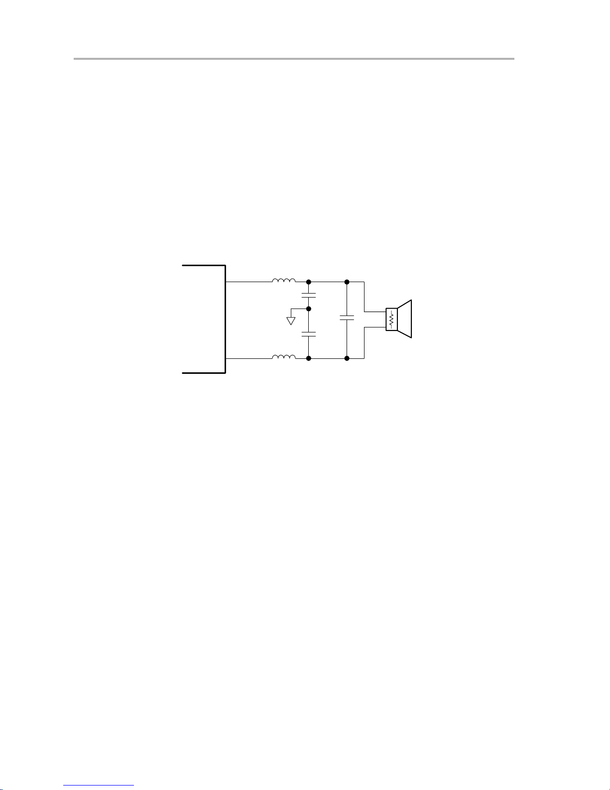
LC filter is shown in Figure 4−9.
Figure 4−9.APA100 Output Filter
TAS51xx
Output A
L
Output B
C1A
C2
C1B
L
R
(Load)
To limit near-field EMI, the loop area of the output switching path through the
inductor and capacitor must be minimized. To minimize the far-field EMI, filter
each output referenced to a clean ground. Capacitors C1A and C1B filter the
outputs referenced to ground. Capacitor C2 adds differential filtering to
minimize the loop area. Also, 100-nF capacitors need to be placed from each
output terminal (where speaker wires leave the board) to a clean ground.
Increasing the capacitors (C1A, C1B, and C2) lowers the cutoff frequency,
which improves EMI performance but also increases current flow in the filter.
The type of inductor is important for limiting EMI. Multiple winding inductors
can be made small, but the multiple windings start to function capacitively at
a lower frequency and do not attenuate as much of the 100-MHz to 500-MHz
harmonics that are needed to eliminate EMI. For additional EMI suppression,
a ferrite bead can be placed in series with the inductors.
The inductor must have 8 µH of inductance or more at 15 A, for overcurrent
(OC) protection to be effective. The TAS5111 data sheet recommends 5 µH
of inductance, but that is for a switching frequency of 380 kHz. The APA100
switches at 250 kHz and needs more inductance to protect the device.
The modulation scheme used by the APA100 (based on the TPA2001D1
modulation scheme) can be used without a filter if EMI and OC protection
are not important. For more information on the filter−free modulation, see
the application section of the TPA2001D1 data sheet.
4-10
Page 33

4.6 Thermal
Thermal
The APA100 thermal issues lie with the TAS5111. The following thermal
calculations and tables are taken from the TAS5111 data sheet. The TAS5111
is designed to be interfaced directly to a heatsink using a thermal interface
compound (for example, Wakefield Engineering type 126 thermal grease.)
The heatsink then absorbs heat from the ICs and couples it to the local air. If
the heatsink is carefully designed, this process can reach equilibrium and heat
can be continually removed from the ICs. Because of the efficiency of the
TAS5111, heatsinks are smaller than those required for linear amplifiers of
equivalent performance. R
is a system thermal resistance from junction to
θ
JA
ambient air. As such, it is a system parameter with roughly the following
components:
- R
(the thermal resistance from junction to case, or in this case the metal
θ
JC
pad)
- Thermal grease thermal resistance
- Heatsink thermal resistance
R
has been provided in the General Information section.
θ
JC
The thermal grease thermal resistance can be calculated from the exposed
pad area and the thermal grease manufacturer’s area thermal resistance
2
(expressed in °C−in
grease with a 0.001-inch thick layer is about 0.054°C−in
/W). The area thermal resistance of the example thermal
2
/W. The approximate
exposed pad area is 0.0164 in2. Dividing the example thermal grease area
resistance by the area of the pad gives the actual resistance through the
thermal grease, 3.3°C/W.
Heatsink thermal resistance is generally predicted by the heatsink vendor,
modeled using a continuous flow dynamics (CFD) model, or measured.
Thus, for a single monaural IC, the system is defined by Equation 9.
+ R
R
JA
q
) thermal greasse resistance ) heatsink resistance.
JC
q
The following table indicates modeled parameters for one TAS5111 IC on a
heatsink. The junction temperature is set at 110°C in both cases while
delivering 70 W RMS into 4-Ω loads with no clipping. It is assumed that the
thermal grease is about 0.001 inch thick (this is critical).
Table 4−1.TAS5111 Thermal Table
Ambient temperature 25°C
Power to load 70 W
Delta T inside package 12.3°C
Delta T through thermal grease 21.1°C
Required heatsink thermal resistance 8.2°C/W
Junction temperature 110°C
System R
R
θ
JA
θ
JA
× power dissipation 85°C
(9)
32-Pin TSSOP
13.2°C/W
Technical Information
4-11
Page 34

Thermal
As an indication of the importance of keeping the thermal grease layer thin, if
the thermal grease layer increases to 0.002 inch thick, the required heatsink
thermal resistance changes to 2.4°C/W.
The large heatsink used for the APA100 EVM is required for full output power
sine waves over temperature. A smaller heatsink can be used for music, which
requires much less average power.
The heatsink should be tight without bending the board or damaging the IC.
However, there should be slight dimpling of the boards around the screws.
Heatsink screws were tightened with a torque of 1.5 inch−pounds on the
APA100 board. A washer and lock−washer can be used to help secure the
heatsink, but is not required in most applications.
4-12
Page 35

Chapter 5
Measured Results
This chapter shows the performance of the APA100 reference design. An
Audio Precision analyzer was used to produce the graphs in this chapter.
Topic Page
5.1 Total Harmonic Distortion + Noise 5-2. . . . . . . . . . . . . . . . . . . . . . . . . . . . . .
5.2 Output Power 5-4. . . . . . . . . . . . . . . . . . . . . . . . . . . . . . . . . . . . . . . . . . . . . . . . .
5.3 Efficiency 5-5. . . . . . . . . . . . . . . . . . . . . . . . . . . . . . . . . . . . . . . . . . . . . . . . . . . .
5.4 Gain and Phase 5-6. . . . . . . . . . . . . . . . . . . . . . . . . . . . . . . . . . . . . . . . . . . . . . .
5.5 Signal−to−Noise Ratio 5-6. . . . . . . . . . . . . . . . . . . . . . . . . . . . . . . . . . . . . . . . .
5.6 Supply Ripple Rejection 5-7. . . . . . . . . . . . . . . . . . . . . . . . . . . . . . . . . . . . . . .
Measured Results
5-1
Page 36
Total Harmonic Distortion + Noise
5.1 Total Harmonic Distortion + Noise
The APA100 has excellent total harmonic distortion + noise (THD+N).
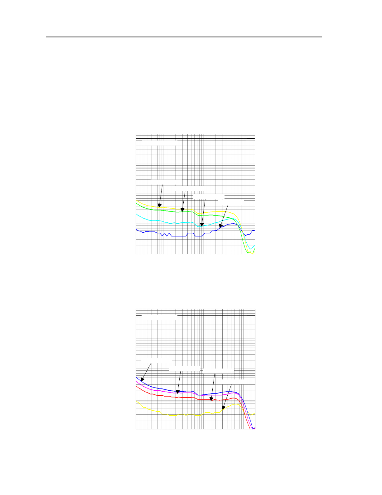
Figure 5−1 and Figure 5−2 show the THD+N versus frequency, and
Figure 5−3 and Figure 5−4 show THD+N vs output power. A 30-kHz
bandwidth limit was used on the audio precision to limit switching frequency
from affecting the measurement.
Figure 5−1.APA100 THD+N vs Frequency With 4-W Load
100
VCC = 29.5 V
10
PO = 70 W
1
PO = 40 W
PO = 10 W
PO = 1 W
0.1
THD+N − Total Harmonic Distortion + Noise − %
0.01
20 100 200 1 k 2 k 20 k
f − Frequency − Hz
Figure 5−2.APA100 THD+N vs Frequency With 8-W Load
100
VCC = 29.5 V
10
PO = 40 W
1
0.1
PO = 20 W
PO = 10 W
PO = 1 W
THD+N − Total Harmonic Distortion + Noise − %
0.01
5-2
20 100 200 1 k 2 k 20 k
f − Frequency − Hz
Page 37
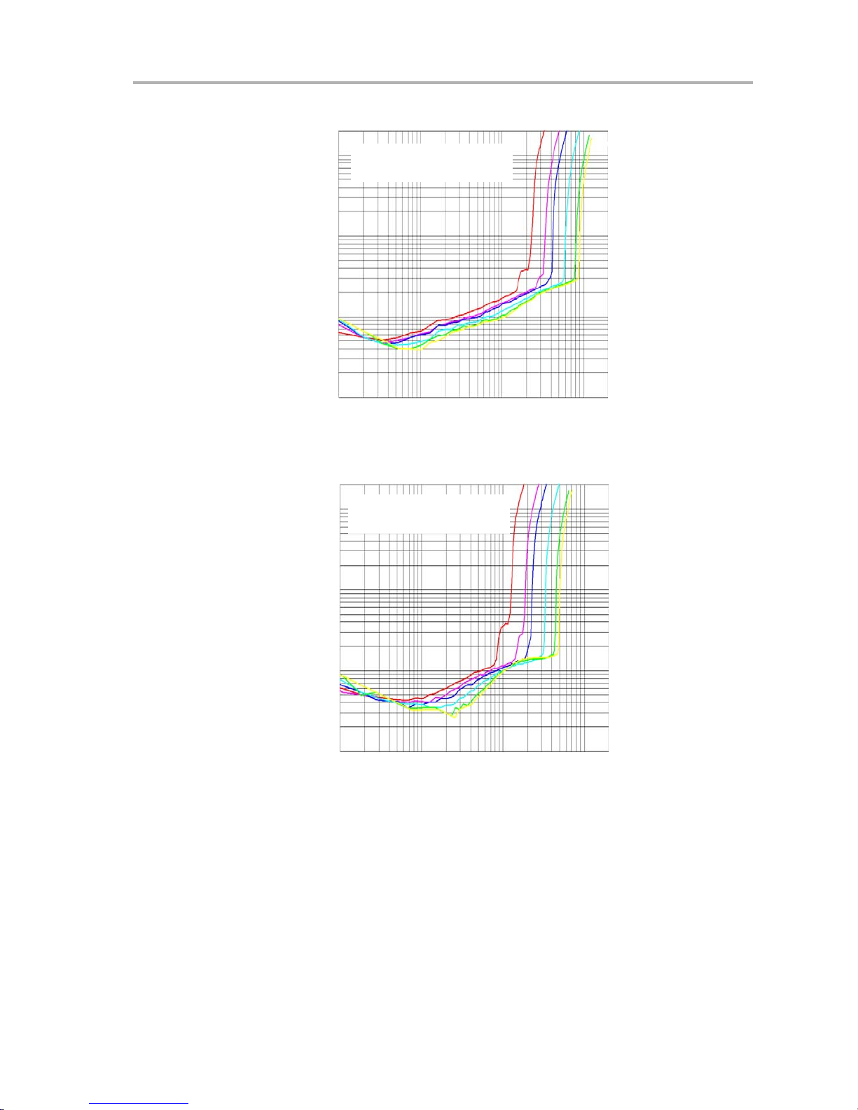
Figure 5−3.APA100 THD+N vs Output Power With 4-W Load
20
f = 1 kHz,
= 15 V, 18 V, 20 V, 24 V,
PV
DD
28 V, 29.5 V
5
1
0.5
0.1
0.05
THD+N − Total Harmonic Distortion + Noise − %
0.01
10 m 1 2 10 20 100 200
PO − Output Power − W
Figure 5−4.APA100 THD+N vs Output Power With 8-W Load
20
f = 1 kHz,
PV
= 15 V, 18 V, 20 V, 24 V,
DD
28 V, 29.5 V
5
Total Harmonic Distortion + Noise
1
0.5
0.1
0.05
THD+N − Total Harmonic Distortion + Noise − %
0.01
10 m 1 2 10 20 100 200
PO − Output Power − W
Measured Results
5-3
Page 38
Output Power
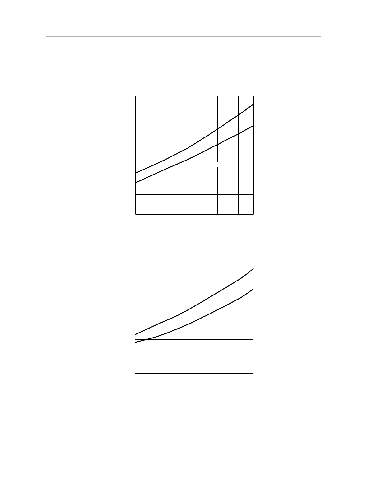
5.2 Output Power
The APA100 can output over 100 W into 4 Ω. The curves in Figure 5−5 and
Figure 5−6 show the output power versus supply voltage.
Figure 5−5.APA100 Output Power vs Supply Voltage With 4-W Load
120
f = 1 kHz
100
PO @ 10% THD
80
60
− Output Power − W
O
40
P
20
PO @ 1% THD
0
18 20 22 24 26 28
−
V
Supply Voltage − V
CC
Figure 5−6.APA100 Output Power vs Supply Voltage With 8-W Load
70
f = 1 kHz
60
50
40
30
− Output Power − W
O
P
20
10
0
18 20 22 24 26 28
PO @ 10% THD
PO @ 1% THD
−
V
Supply Voltage − V
CC
5-4
Page 39

5.3 Efficiency
The APA100 is a highly efficient class-D audio power amplifier. The efficiency
is greater than 85% efficient with 4- or 8-Ω load. The efficiency plot is shown
in Figure 5−7.
Figure 5−7.APA100 Efficiency vs Output Power With 4-W Load
100
90
80
70
60
50
40
30
20
− System Output Stage Efficiency − %
10
0
01020304050607080
PO − Output Power − W
f = 1 kHz,
R
= 4 ,
L
= 755C
T
C
Efficiency
Measured Results
5-5
Page 40
Gain and Phase Response
5.4 Gain and Phase Response
The APA100 is a closed−loop, class-D audio power amplifier with an LC output
filter. The output filter and the 39-kHz loop bandwidth limit the bandwidth of the
APA100 reference design. The gain versus frequency curve is shown in
Figure 5−8. The 4-Ω curve rolls off sooner than the 8-Ω curve.
Figure 5−8.APA100 Gain vs Frequency With 4-W and 8-W Load
40
8
35
30
25
20
Gain − dB
15
10
5
0
20 100 200 1 k 2 k 10 k 20 k
5.5 Signal-to-Noise Ratio (SNR)
The APA100 has low noise and a wide output swing. The noise does not
increase with output power making the signal-to-noise ratio (SNR) just before
clipping good for this type of amplifier. The noise was measured with an
A-weighted filter to be 350 µV rms. The amplifier can output 19 Vrms. This
makes the SNR 95 dB at 19-Vrms output.
4
f − Frequency − Hz
5-6
Page 41
Supply Ripple Rejection
5.6 Supply Ripple Rejection
The APA100 uses a closed loop which keeps the gain from changing with
supply voltage and improves the supply ripple rejection ratio (k
open−loop class-D amplifier. The supply ripple rejection ratio versus
frequency curve is shown in Figure 5−9.
Figure 5−9. APA100 Supply Ripple Rejection Ratio vs Frequency With 8-W Load
0
−10
−20
−30
−40
−50
−60
− Supply Voltage Rejection Ratio − V
SR
−70
k
SRR
) over an
−80
20 100 200 1 k 2 k 10 k 20 k
f − Frequency − Hz
Measured Results
5-7
Page 42

5-8
 Loading...