

TPA2000D1-Q1
2-W FILTERLESS MONO CLASS-D AUDIO POWER AMPLIFIER
SGLS137 – SEPTEMBER 2002
D Qualification in Accordance With
AEC-Q100
†
D Qualified for Automotive Applications
D Customer-Specific Configuration Control
Can Be Supported Along With
Major-Change Approval
D ESD Protection Exceeds 2000 V Per
MIL-STD-883, Method 3015; Exceeds 200 V
D 4 mm × 4 mm MicroStar Junior BGA and
TSSOP Package Options
D 2 W Into a 4-Ω Speaker (THD+N<1%)
D <0.2% THD+N at 1.5 W, 1 kHz, Into a 4-Ω
Load
D Integrated Depop Circuitry
D Short-Circuit Protection (Short to Battery,
Ground, and Load)
Using Machine Model (C = 200 pF, R = 0)
D Modulation Scheme Optimized to Operate
Without a Filter
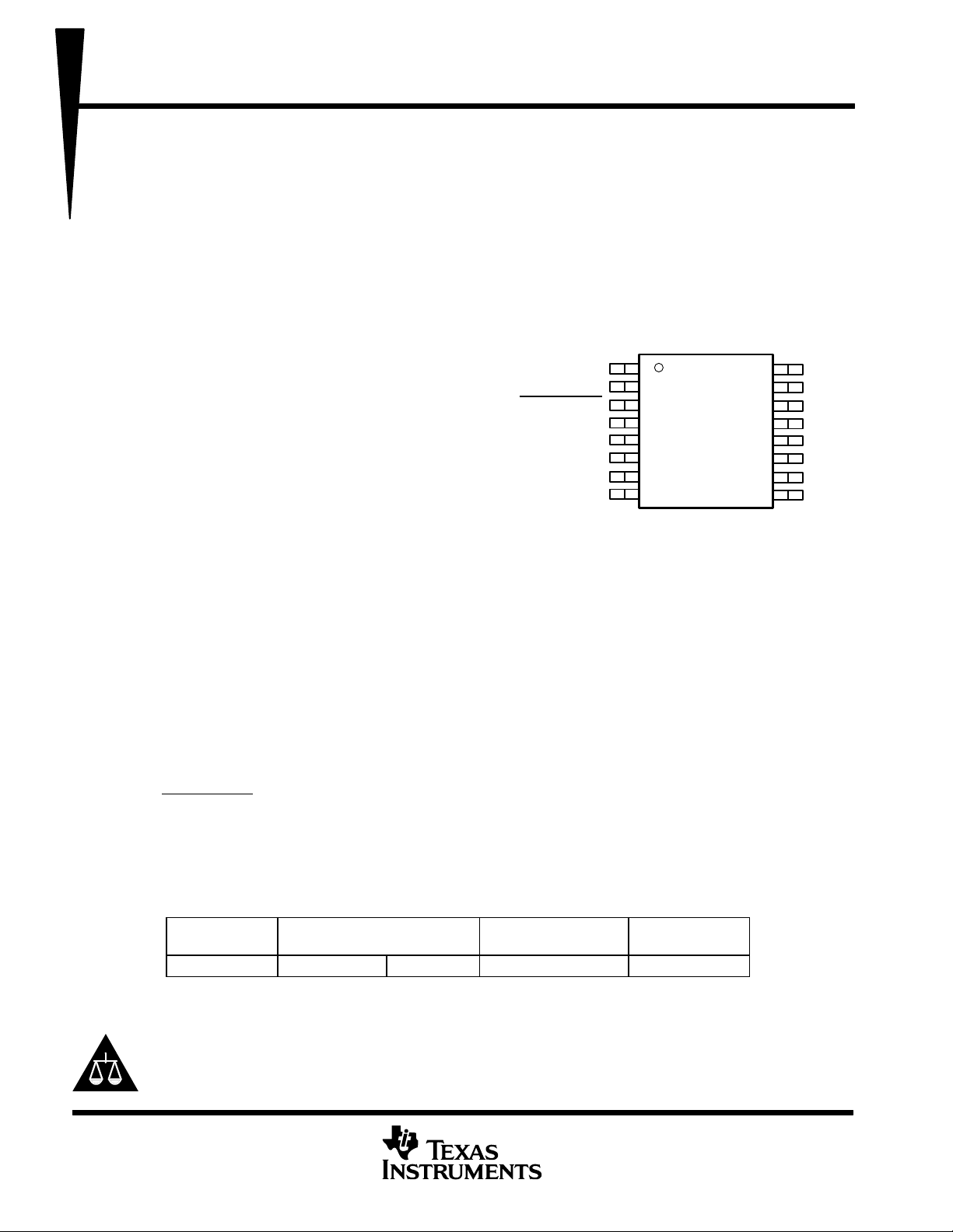
PW PACKAGE
(TOP VIEW)
D Extremely Efficient Third Generation 5-V
Class-D Technology:
– Low-Supply Current (No Filter) ...4 mA
– Low-Supply Current (Filter) . . . 7.5 mA
– Low-Shutdown Current . . . 0.05 µA
– Low-Noise Floor ...40 µV
RMS
(No-Weighting Filter)
– Maximum Efficiency Into 8 Ω, 75 – 85 %
– 4 Internal Gain Settings ...6 – 23.5 dB
INP
INN
SHUTDOWN
GAIN0
GAIN1
PV
DD
OUTP
PGND
1
2
3
4
5
6
7
8
– PSSR . . . –77 dB
†
Contact factory for details. Q100 qualification data available on
request.
description
The TP A2000D1 is a 2-W mono bridge-tied-load (BTL) class-D amplifier designed to drive a speaker with at least
4-Ω impedance. The amplifier uses TI’s third generation modulation technique, which results in improved efficiency
and SNR. It also allows the device to be connected directly to the speaker without the use of the LC output filter
commonly associated with class-D amplifiers (this will result in EMI which must be shielded at the system level).
These features make the device ideal for use in devices where high-efficiency is needed to extend battery run time.
16
15
14
13
12
11
10
9
BYPASS
AGND
COSC
ROSC
V
DD
PV
DD
OUTN
PGND
The gain of the amplifier is controlled by two input terminals, GAIN1, and GAIN0. This allows the amplifier to be
configured for a gain of 6, 12, 18, and 23.5 dB. The differential input terminals are high-impedance CMOS inputs,
and can be used as summing nodes.
The class-D BTL amplifier includes depop circuitry to reduce the amount of turnon pop at power up, and when
cycling SHUTDOWN
.
The TPA2000D1 is available in the 16-pin TSSOP and MicroStar Junior BGA packages that will drive 2 W of
continuous output power into a 4-Ω load. TPA2000D1T operates over an ambient temperature range of –40°C to
105°C.
ORDERING INFORMATION
T
A
–40°C to 105°C TSSOP (PW) Tape and Reel TPA2000D1TPWRQ1 20001T
‡
Package drawings, standard packing quantities, thermal data, symbolization, and PCB design guidelines are
available at www.ti.com/sc/package.
Please be aware that an important notice concerning availability, standard warranty, and use in critical applications of
Texas Instruments semiconductor products and disclaimers thereto appears at the end of this data sheet.
PRODUCTION DATA information is current as of publication date.
Products conform to specifications per the terms of Texas Instruments
standard warranty. Production processing does not necessarily include
testing of all parameters.
PACKAGE
‡
ORDERABLE
PART NUMBER
TOP-SIDE
MARKING
Copyright 2002, Texas Instruments Incorporated
POST OFFICE BOX 655303 • DALLAS, TEXAS 75265
1
TPA2000D1-Q1
2-W FILTERLESS MONO CLASS-D AUDIO POWER AMPLIFIER
SGLS137 – SEPTEMBER 2002
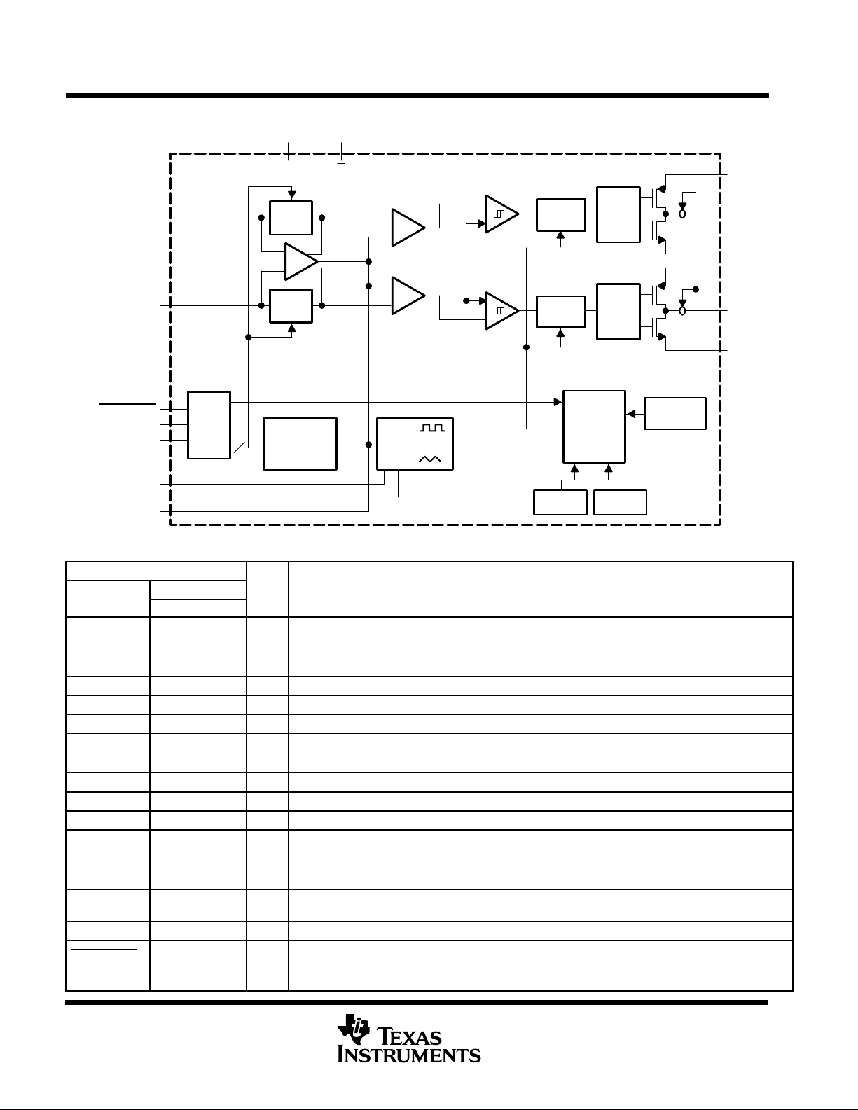
functional block diagram
DD
V
DD
AGNDV
PV
DD
INN
INP
SHUTDOWN
GAIN1
GAIN0
COSC
ROSC
BYPASS
SD
Gain
2
Gain
Adjust
_
+
_
+
Gain
Adjust
Biases
and
References
_
+
+
_
Ramp
Generator
+
_
_
+
Deglitch
Logic
Deglitch
Logic
Thermal VDD ok
Terminal Functions
TERMINAL
NAME
NO.
GQC PW
A3 – A5,
AGND
B2 – B6
C2 – C6
D2 – D4
BYPASS A6 16 I Connect capacitor to ground for BYPASS voltage filtering.
COSC B7 14 I Connect capacitor to ground to set oscillation frequency.
GAIN0 C1 4 I Bit 0 of gain control (TTL logic level)
GAIN1 D1 5 I Bit 1 of gain control (TTL logic level)
INN A1 2 I Negative differential input
INP A2 1 I Positive differential input
OUTN G7 10 O Negative BTL output
OUTP G1 7 O Positive BTL output
D5, D6
PGND
E2 – E6
F2 – F6
8, 9 I High-current grounds
G2 – G6
PV
DD
E1, E7,
F1, F7
6, 11 I High-current power supplies
ROSC C7 13 I Connect resistor to ground to set oscillation frequency.
SHUTDOWN B1 3 I
V
DD
D7 12 I Analog power supply
I/O DESCRIPTION
15 I Analog ground
Places the amplifier in shutdown mode if a TTL logic low is placed on this terminal, and normal operation
if a TTL logic high is placed on this terminal.
Drive
Drive
Start-Up
Protection
Logic
Gate
Gate
OC
Detect
OUTN
PGND
PV
DD
OUTP
PGND
2
POST OFFICE BOX 655303 • DALLAS, TEXAS 75265
TPA2000D1-Q1
ББББББББББББББББББББББББББББ
БББББББББББББББББББ
ББББББББББББББББББББББББББББ
ÁÁÁ
ÁÁÁ
ÁÁÁ
ÁÁÁ
ÁÁÁ
ÁÁÁ
ББББББ
ÁÁÁ
ББББББ
ÁÁÁ
ББББББ
ÁÁÁ
ББББББ
ÁÁÁ
ББББББ
ÁÁÁ
ББББББ
ÁÁÁ
ББББББ
2-W FILTERLESS MONO CLASS-D AUDIO POWER AMPLIFIER
SGLS137 – SEPTEMBER 2002
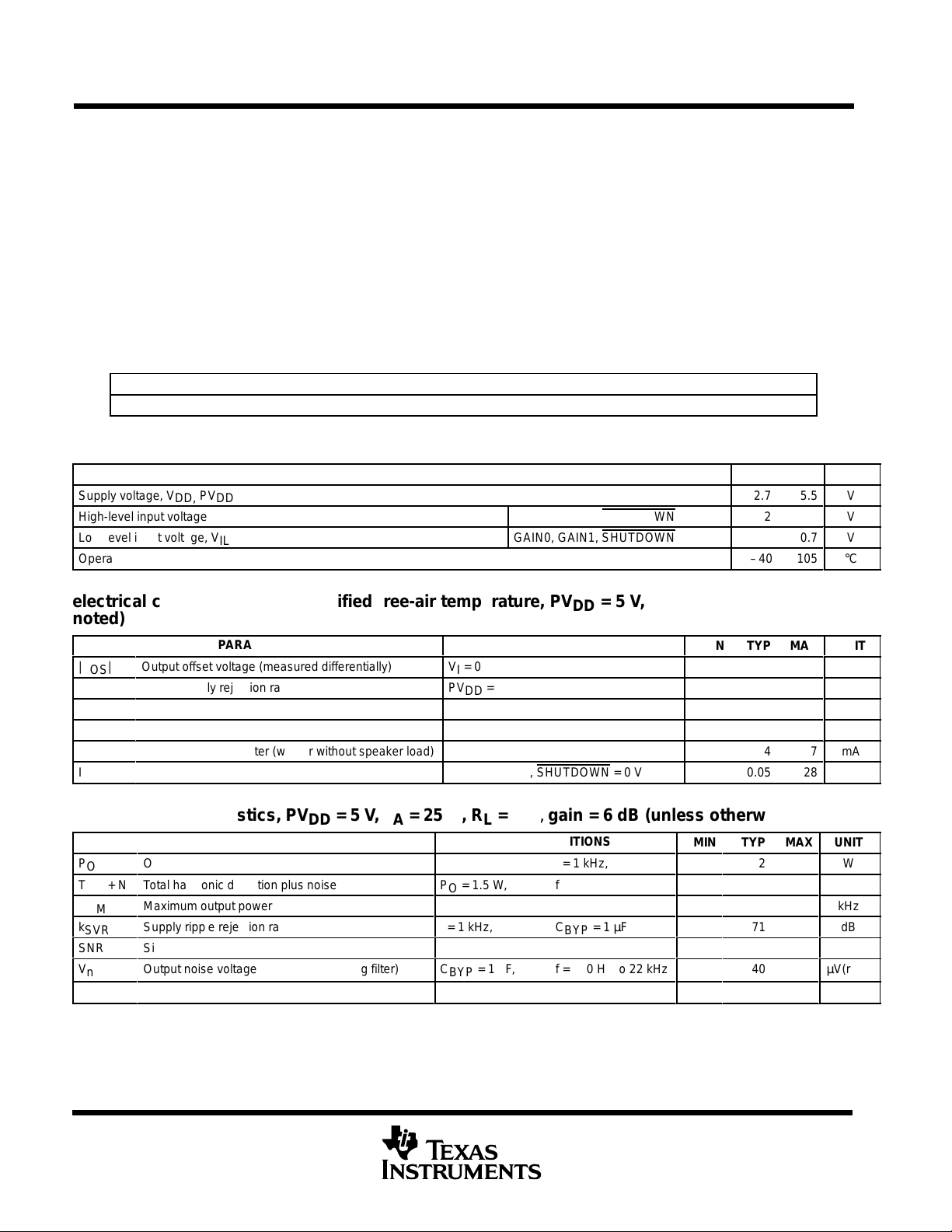
absolute maximum ratings over operating free-air temperature range (unless otherwise noted)
Supply voltage, V
Input voltage, V
PVDD –0.3 V to 5.5 V. . . . . . . . . . . . . . . . . . . . . . . . . . . . . . . . . . . . . . . . . . . . . . . . . . . . . . . .
DD,
–0.3 V to VDD +0.3 V. . . . . . . . . . . . . . . . . . . . . . . . . . . . . . . . . . . . . . . . . . . . . . . . . . . . . . . . . . . .
I
{
Continuous total power dissipation (see Dissipation Rating Table). . . . . . . . . . . . . . . . . . . . . . . . . . . . . . . . . . . . .
Operating free-air temperature range, T
Operating junction temperature range, T
Storage temperature range, T
–65°C to 150°C. . . . . . . . . . . . . . . . . . . . . . . . . . . . . . . . . . . . . . . . . . . . . . . . . . .
stg
–40°C to 105°C. . . . . . . . . . . . . . . . . . . . . . . . . . . . . . . . . . . . . . . . . . .
A
–40°C to 115°C. . . . . . . . . . . . . . . . . . . . . . . . . . . . . . . . . . . . . . . . . . .
J
Lead temperature 1,6 mm (1/16 inch) from case for 10 seconds 260°C. . . . . . . . . . . . . . . . . . . . . . . . . . . . . . . .
{
Stresses beyond those listed under “absolute maximum ratings” may cause permanent damage to the device. These are stress ratings only, and
functional operation of the device at these or any other conditions beyond those indicated under “recommended operating conditions” is not implied.
Exposure to absolute-maximum-rated conditions for extended periods may affect device reliability.
DISSIPATION RATING TABLE
PACKAGE
TA ≤ 25°C DERATING FACTOR TA = 70°C TA = 85°C TA = 105°C
PW 774 mW 6.19 mW/°C 495 mW 402 mW 279 mW
recommended operating conditions
MIN MAX UNIT
Supply voltage, V
High-level input voltage, V
Low-level input voltage, V
Operating free-air temperature, T
DD,
PV
DD
IH
IL
2.7
5.5
GAIN0, GAIN1, SHUTDOWN
GAIN0, GAIN1, SHUTDOWN
A
–40
2
0.7
105
V
V
V
°C
electrical characteristics at specified free-air temperature, PVDD = 5 V, TA = 25°C (unless otherwise
noted)
PARAMETER TEST CONDITIONS
|VOS|
PSRR
|IIH|
|IIL|
I
DD
I
DD(SD)
Output offset voltage (measured differentially)
Power supply rejection ratio
High-level input current
Low-level input current
Supply current, no filter (with or without speaker load)
Supply current, shutdown mode
operating characteristics, PVDD = 5 V, T
PARAMETER TEST CONDITIONS
P
O
THD + N
B
OM
k
SVR
SNR
V
n
Z
i
Output power
Total harmonic distortion plus noise
Maximum output power bandwidth
Supply ripple rejection ratio
Signal-to-noise ratio
Output noise voltage (no-noise weighting filter)
Input impedance
= 25°C, R
A
VI = 0 V, AV = any gain
PVDD = 4.9 V to 5.1 V
PVDD = 5.5, VI = PV
DD
PVDD = 5.5, VI = 0 V
GAIN0, GAIN1, SHUTDOWN = 0 V
= 4 Ω, gain = 6 dB (unless otherwise noted)
L
THD = 1%,
PO = 1.5 W,
f = 1 kHz,
f = 20 Hz to 20 kHz
THD = 1%,
f = 1 kHz,
C
= 1 µF,
BYP
C
= 1 µF
BYP
f = <10 Hz to 22 kHz
MIN TYP MAX UNIT
25
mV
77
4
0.05
28
dB
1
µA
1
µA
7
mA
µA
MIN TYP MAX UNIT
2
W
<0.2%
20
71
95
40
>15
kHz
dB
dB
µV(rms)
kΩ
POST OFFICE BOX 655303 • DALLAS, TEXAS 75265
3
TPA2000D1-Q1
ÁÁÁ
ÁÁÁ
ÁÁÁ
ÁÁÁ
ÁÁÁ
ÁÁÁ
ÁÁÁ
ББББББ
ÁÁÁ
ББББББ
ÁÁÁ
ББББББ
ÁÁÁ
ББББББ
ÁÁÁ
ББББББ
ÁÁÁ
ББББББ
2-W FILTERLESS MONO CLASS-D AUDIO POWER AMPLIFIER
SGLS137 – SEPTEMBER 2002
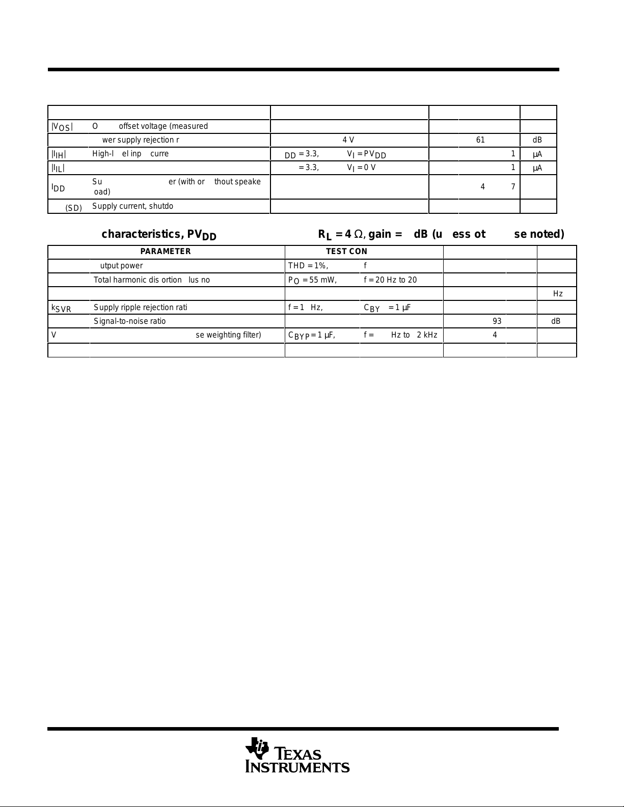
electrical characteristics at specified free-air temperature, PVDD = 3.3 V , TA = 25°C (unless otherwise
noted)
|VOS|
PSRR
|IIH|
|IIL|
I
DD
I
DD(SD)
PARAMETER TEST CONDITIONS
Output offset voltage (measured differentially)
Power supply rejection ratio
High-level input current
Low-level input current
Supply current, no filter (with or without speaker
load)
Supply current, shutdown mode
VI = 0 V, AV = any gain
PVDD = 3.2 V to 3.4 V
PVDD = 3.3, VI = PV
DD
PVDD = 3.3, VI = 0 V
MIN TYP MAX UNIT
25
mV
61
4
0.05
28
dB
1
µA
1
µA
7
mA
µA
operating characteristics, PVDD = 3.3 V, T
PARAMETER TEST CONDITIONS
P
O
THD + N
B
OM
k
SVR
SNR
V
n
Z
i
Output power
Total harmonic distortion plus noise
Maximum output power bandwidth
Supply ripple rejection ratio
Signal-to-noise ratio
Output noise voltage (no-noise weighting filter)
Input impedance
= 25°C, R
A
THD = 1%,
PO = 55 mW,
THD = 0.7%
f = 1 kHz,
C
BYP
= 4 Ω, gain = 6 dB (unless otherwise noted)
L
MIN TYP MAX UNIT
f = 1 kHz
f = 20 Hz to 20 kHz
850
<0.2%
20
C
BYP
= 1 µF
61
93
= 1 µF,
f = <10 Hz to 22 kHz
40
>15
mW
kHz
dB
dB
µV(rms)
kΩ
4
POST OFFICE BOX 655303 • DALLAS, TEXAS 75265
TPA2000D1-Q1
2-W FILTERLESS MONO CLASS-D AUDIO POWER AMPLIFIER
SGLS137 – SEPTEMBER 2002
APPLICATION INFORMATION
eliminating the output filter with the TPA2000D1
This section will focus on why the user can eliminate the output filter with the TPA2000D1.
effect on audio
The class-D amplifier outputs a pulse-width modulated (PWM) square wave, which is the sum of the switching
waveform and the amplified input audio signal. The human ear acts as a band-pass filter such that only the
frequencies between approximately 20 Hz and 20 kHz are passed. The switching frequency components are much
greater than 20 kHz, so the only signal heard is the amplified input audio signal.
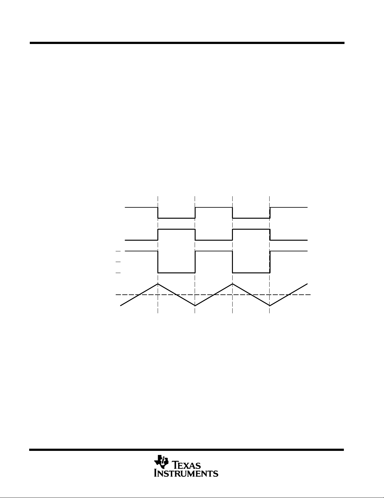
traditional class-D modulation scheme
The traditional class-D modulation scheme, which is used in the TP A005Dxx family , has a differential output where
each output is 180 degrees out of phase and changes from ground to the supply voltage, V
differential pre-filtered output varies between positive and negative V
, where filtered 50% duty cycle yields 0 V
DD
across the load. The traditional class-D modulation scheme with voltage and current waveforms is shown in Figure
1. Note that even at an average of 0 V across the load (50% duty cycle), the current to the load is high, causing high
loss, thus causing a high supply current.
. Therefore, the
DD
OUTP
OUTN
+5 V
Differential Voltage
Across Load
O V
–5 V
Current
Figure 1. Traditional Class-D Modulation Scheme’s Output Voltage and Current Waveforms Into an Inductive
Load With No Input
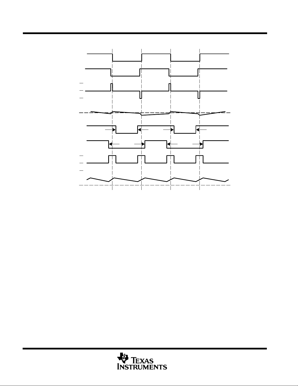
TPA2000D1 modulation scheme
The TPA2000D1 uses a modulation scheme that still has each output switching from 0 to the supply voltage.
However, OUTP and OUTN are now in phase with each other with no input. The duty cycle of OUTP is greater than
50% and OUTN is less than 50% for positive voltages. The duty cycle of OUTP is less than 50% and OUTN is greater
than 50% for negative voltages. The voltage across the load sits at 0 V throughout most of the switching period
greatly reducing the switching current, which reduces any I
2
R losses in the load.
POST OFFICE BOX 655303 • DALLAS, TEXAS 75265
5
TPA2000D1-Q1
2-W FILTERLESS MONO CLASS-D AUDIO POWER AMPLIFIER
SGLS137 – SEPTEMBER 2002
APPLICATION INFORMATION
OUTP
OUTN
Differential
Voltage
Across
Load
+5 V
0 V
–5 V
Current
OUTP
Output = 0 V
Differential
Voltage
Across
Load
OUTN
+5 V
0 V
–5 V
Current
Output > 0 V
Figure 2. The TPA2000D1 Output Voltage and Current Waveforms Into an Inductive Load
efficiency: why you must use a filter with the traditional class-D modulation scheme
The main reason that the traditional class-D amplifier needs an output filter is that the switching waveform results
in maximum current flow. This causes more loss in the load, which causes lower ef ficiency. The ripple current is large
for the traditional modulation scheme because the ripple current is proportional to voltage multiplied by the time at
that voltage. The differential voltage swing is 2 ×V
and the time at each voltage is half the period for the traditional
DD
modulation scheme. An ideal LC filter is needed to store the ripple current from each half cycle for the next half cycle,
while any resistance causes power dissipation. The speaker is both resistive and reactive, whereas an LC filter is
almost purely reactive.
The TP A2000D1 modulation scheme has very little loss in the load without a filter because the pulses are very short
and the change in voltage is V
instead of 2 × VDD. As the output power increases, the pulses widen making the
DD
ripple current larger. Ripple current could be filtered with an LC filter for increased ef ficiency, but for most applications
the filter is not needed.
An LC filter with a cut-off frequency less than the class-D switching frequency allows the switching current to flow
through the filter instead of the load. The filter has less resistance than the speaker that results in less power
dissipated, which increases efficiency.
6
POST OFFICE BOX 655303 • DALLAS, TEXAS 75265

TPA2000D1-Q1
2-W FILTERLESS MONO CLASS-D AUDIO POWER AMPLIFIER
SGLS137 – SEPTEMBER 2002
APPLICATION INFORMATION
effects of applying a square wave into a speaker
Audio specialists have advised for years not to apply a square wave to speakers. If the amplitude of the waveform
is high enough and the frequency of the square wave is within the bandwidth of the speaker, the square wave could
cause the voice coil to jump out of the air gap and/or scar the voice coil. A 250-kHz switching frequency , however ,
is not significant because the speaker cone movement is proportional to 1/f
Therefore, the amount of cone movement at the switching frequency is very small. However, damage could occur
to the speaker if the voice coil is not designed to handle the additional power. To size the speaker for added power,
the ripple current dissipated in the load needs to be calculated by subtracting the theoretical supplied power (P
THEORETICAL
) from the actual supply power (P
) at maximum output power (P
SUP
dissipated in the speaker is the inverse of the measured efficiency (η
(η
THEORETICAL
SPKR
) all multiplied by P
= P
SUP
– P
.
OUT
SUP THEORETICAL
(at max output power)
2
for frequencies beyond the audio band.
). The switching power
OUT
MEASURED
) minus the theoretical efficiency
SUP
(1)P
SPKR
SPKR
= P
OUT(PSUP
= P
OUT
(1/η
MEASURED
/ P
OUT
– P
SUP THEORETICAL
– 1/η
THEORETICAL
/ P
) (at max output power)
OUT
) (at max output power)
The maximum efficiency of the TPA2000D1 with an 8-Ω load is 85%. Using equation 3 with the efficiency at
maximum power (78%), we see that there is an additional 106 mW dissipated in the speaker. The added power
dissipated in the speaker is not an issue as long as it is taken into account when choosing the speaker.
when to use an output filter
Design the TP A2000D1 without the filter if the traces from amplifier to speaker are short. The TPA2000D1 passed
FCC and CE radiated emissions with no shielding with speaker wires eight inches long or less. Notebook PCs and
powered speakers where the speaker is in the same enclosure as the amplifier are good applications for class-D
without a filter.
A ferrite bead filter can often be used if the design is failing radiated emissions without a filter, and the frequency
sensitive circuit is greater than 1 MHz. This is good for circuits that just have to pass FCC and CE because FCC
and CE only test radiated emissions greater than 30 MHz. If choosing a ferrite bead, choose one with high
impedance at high frequencies, but very low impedance at low frequencies.
Use an output filter if there are low frequency (<1 MHz) EMI sensitive circuits and/or there are long leads from
amplifier to speaker.
gain setting via GAIN0 and GAIN1 inputs
The gain of the TPA2000D1 is set by two input terminals, GAIN0 and GAIN1.
The gains listed in T able 1 are realized by changing the taps on the input resistors inside the amplifier . This causes
the input impedance (Z
resistors, so the actual gain distribution from part-to-part is quite good. However, the input impedance may shift by
30% due to shifts in the actual resistance of the input resistors.
) to be dependent on the gain setting. The actual gain settings are controlled by ratios of
i
(2)P
(3)P
For design purposes, the input network (discussed in the next section) should be designed assuming an input
impedance of 20 kΩ, which is the absolute minimum input impedance of the TP A2000D1. At the higher gain settings,
the input impedance could increase as high as 115 kΩ.
POST OFFICE BOX 655303 • DALLAS, TEXAS 75265
7

TPA2000D1-Q1
GAIN0
GAIN1
2-W FILTERLESS MONO CLASS-D AUDIO POWER AMPLIFIER
SGLS137 – SEPTEMBER 2002
APPLICATION INFORMATION
Table 1. Gain Settings
AMPLIFIER GAIN
GAIN0 GAIN1
0 0 6 104
0 1 12 74
1 0 18 44
1 1 23.5 24
(dB)
TYP TYP
INPUT IMPEDANCE
(kΩ)
input resistance
Each gain setting is achieved by varying the input resistance of the amplifier, which can range from its smallest value
to over six times that value. As a result, if a single capacitor is used in the input high-pass filter, the –3 dB or cutof f
frequency will also change by over six times.
Z
f
C
i
Input
Signal
IN
The –3-dB frequency can be calculated using equation 4.
Z
i
f
–3dB
input capacitor, C
+
i
2p C
1
ǒ
R ø Z
i
Ǔ
i
In the typical application an input capacitor (C
dc level for optimum operation. In this case, C
with the corner frequency determined in equation 5.
+
2p Z
1
C
i
i
f
c
(4)
) is required to allow the amplifier to bias the input signal to the proper
i
and the input impedance of the amplifier (Zi) form a high-pass filter
i
–3 dB
(5)
f
c
8
POST OFFICE BOX 655303 • DALLAS, TEXAS 75265

TPA2000D1-Q1
2-W FILTERLESS MONO CLASS-D AUDIO POWER AMPLIFIER
SGLS137 – SEPTEMBER 2002
APPLICATION INFORMATION
input capacitor, C
(continued)
i
The value of Ci is important, as it directly affects the bass (low frequency) performance of the circuit. Consider the
example where Z
is 20 kΩ and the specification calls for a flat bass response down to 80 Hz. Equation 5 is
i
reconfigured as equation 6.
1
+
C
i
2p Z
f
c
i
In this example, C
and will be constant, use Z
from the input source through the input network (C
is 0.1 µF, so one would likely choose a value in the range of 0.1 µF to 1 µF. If the gain is known
i
from T able 1 to calculate Ci. A further consideration for this capacitor is the leakage path
i
) and the feedback network to the load. This leakage current
i
creates a dc offset voltage at the input to the amplifier that reduces useful headroom, especially in high gain
applications. For this reason a low-leakage tantalum or ceramic capacitor is the best choice. When polarized
capacitors are used, the positive side of the capacitor should face the amplifier input in most applications as the dc
level there is held at V
/2, which is likely higher than the source dc level. Note that it is important to confirm the
DD
capacitor polarity in the application.
must be 10 times smaller than the bypass capacitor to reduce clicking and popping noise from power on/off and
C
i
entering and leaving shutdown. After sizing C
for a given cutoff frequency, size the bypass capacitor to 10 times
i
that of the input capacitor.
/ 10
BYP
power supply decoupling, C
S
The TP A2000D1 is a high-performance CMOS audio amplifier that requires adequate power supply decoupling to
ensure the output total harmonic distortion (THD) is as low as possible. Power supply decoupling also prevents
oscillations for long lead lengths between the amplifier and the speaker. The optimum decoupling is achieved by
using two capacitors of different types that target different types of noise on the power supply leads. For higher
frequency transients, spikes, or digital hash on the line, a good low equivalent-series-resistance (ESR) ceramic
capacitor, typically 0.1 µF placed as close as possible to the device V
lead works best. For filtering
DD
lower-frequency noise signals, a larger aluminum electrolytic capacitor of 10 µF or greater placed near the audio
power amplifier is recommended.
(6)
(7)Ci ≤ C
midrail bypass capacitor, C
The midrail bypass capacitor (C
start-up or recovery from shutdown mode, C
BYP
) is the most critical capacitor and serves several important functions. During
BYP
determines the rate at which the amplifier starts up. The second
BYP
function is to reduce noise produced by the power supply caused by coupling into the output drive signal. This noise
is from the midrail generation circuit internal to the amplifier, which appears as degraded PSRR and THD+N.
Bypass capacitor (C
) values of 0.47-µF to 1-µF ceramic or tantalum low-ESR capacitors are recommended for
BYP
the best THD and noise performance.
Increasing the bypass capacitor reduces clicking and popping noise from power on/off and entering and leaving
shutdown. To have minimal pop, C
≥ 10 × C
BYP
i
should be 10 times larger than Ci.
BYP
POST OFFICE BOX 655303 • DALLAS, TEXAS 75265
(8)C
9

TPA2000D1-Q1
2-W FILTERLESS MONO CLASS-D AUDIO POWER AMPLIFIER
SGLS137 – SEPTEMBER 2002
APPLICATION INFORMATION
differential input
The differential input stage of the amplifier cancels any noise that appears on both input lines of the channel. T o use
the TP A2000D1 EVM with a differential source, connect the positive lead of the audio source to the INP input and
the negative lead from the audio source to the INN input. To use the TPA2000D1 with a single-ended source, ac
ground the INN input through a capacitor and apply the audio single to the input. In a single-ended input application,
the INN input should be ac-grounded at the audio source instead of at the device input for best noise performance.
shutdown modes
The TP A2000D1 employs a shutdown mode of operation designed to reduce supply current (IDD) to the absolute
minimum level during periods of nonuse for battery-power conservation. The SHUTDOWN
be held high during normal operation when the amplifier is in use. Pulling SHUTDOWN
mute and the amplifier to enter a low-current state, I
DD(SD)
= 1 µA. SHUTDOWN should never be left unconnected
because amplifier operation would be unpredictable.
using low-ESR capacitors
input terminal should
low causes the outputs to
Low-ESR capacitors are recommended throughout this application section. A real (as opposed to ideal) capacitor
can be modeled simply as a resistor in series with an ideal capacitor. The voltage drop across this resistor minimizes
the beneficial effects of the capacitor in the circuit. The lower the equivalent value of this resistance the more the
real capacitor behaves like an ideal capacitor.
evaluation circuit
OUT+
U1
IN–
IN+
SHUTDOWN
V
DD
R2
120 kΩ
S1
R3
120 kΩ
J1
J2
R4
120 kΩ
C8
10 µF
C3
1 µF
C4
1 µF
C2
1 µF
1
INP
2
INN
3
SHUTDOWN
4
GAIN0
5
GAIN1
6
PV
DD
7
OUTP
8
PGND
TPA2000D1
BYPASS
AGND
COSC
ROSC
V
DD
PV
DD
OUTN
PGND
16
15
14
13
12
11
10
9
C7
1 µF
C1
220 pF
120 kΩ
C6
1 µF
C5
1 µF
R1
V
DD
OUT–
GND
GND
NOTE: R1, R2, and R3 are used in the EVM but are not required for normal applications.
10
POST OFFICE BOX 655303 • DALLAS, TEXAS 75265

TPA2000D1-Q1
2-W FILTERLESS MONO CLASS-D AUDIO POWER AMPLIFIER
SGLS137 – SEPTEMBER 2002
APPLICATION INFORMATION
Table 2. TPA2000D1 Evaluation Bill of Materials
REFERENCE DESCRIPTION SIZE QUANTITY MANUFACTURER P ART NUMBER
C1 – C6 Capacitor, ceramic, 1 µF, +80%/–20%, Y5V, 16 V 0805 6 Murata GRM40-Y5V105Z16
C7 Capacitor, ceramic, 10 µF, +80%/–20%, Y5V, 16 V 1210 1 Murata GRM235-Y5V106Z16
C8 Capacitor, ceramic, 220 pF, ±10%, XICON, 50 V 0805 1 Mouser 140-CC501B221K
R1†, R2†,
R3†, R4
U1 IC, TPA2000D1, audio power amplifier, 2-W, single
†
These components are used in the EVM, but they are not required for normal applications.
Resistor, chip, 120 kΩ, 1/10 W, 5%, XICON 0805 4 Mouser 260–120K
channel, class-D
24-pin
TSSOP
1 TI TPA2000D1PW
POST OFFICE BOX 655303 • DALLAS, TEXAS 75265
11

TPA2000D1-Q1
2-W FILTERLESS MONO CLASS-D AUDIO POWER AMPLIFIER
SGLS137 – SEPTEMBER 2002
MECHANICAL DATA
PW (R-PDSO-G**) PLASTIC SMALL-OUTLINE PACKAGE
14 PINS SHOWN
0,65
1,20 MAX
14
0,30
0,19
8
4,50
4,30
PINS **
7
Seating Plane
0,15
0,05
8
1
A
DIM
6,60
6,20
14
0,10
M
0,10
0,15 NOM
0°–ā8°
2016
Gage Plane
24
0,25
0,75
0,50
28
A MAX
A MIN
NOTES: A. All linear dimensions are in millimeters.
B. This drawing is subject to change without notice.
C. Body dimensions do not include mold flash or protrusion not to exceed 0,15.
D. Falls within JEDEC MO-153
3,10
2,90
5,10
4,90
5,10
4,90
6,60
6,40
7,90
7,70
9,80
9,60
4040064/F 01/97
12
POST OFFICE BOX 655303 • DALLAS, TEXAS 75265

IMPORTANT NOTICE
Texas Instruments Incorporated and its subsidiaries (TI) reserve the right to make corrections, modifications,
enhancements, improvements, and other changes to its products and services at any time and to discontinue
any product or service without notice. Customers should obtain the latest relevant information before placing
orders and should verify that such information is current and complete. All products are sold subject to TI’s terms
and conditions of sale supplied at the time of order acknowledgment.
TI warrants performance of its hardware products to the specifications applicable at the time of sale in
accordance with TI’s standard warranty . Testing and other quality control techniques are used to the extent TI
deems necessary to support this warranty . Except where mandated by government requirements, testing of all
parameters of each product is not necessarily performed.
TI assumes no liability for applications assistance or customer product design. Customers are responsible for
their products and applications using TI components. T o minimize the risks associated with customer products
and applications, customers should provide adequate design and operating safeguards.
TI does not warrant or represent that any license, either express or implied, is granted under any TI patent right,
copyright, mask work right, or other TI intellectual property right relating to any combination, machine, or process
in which TI products or services are used. Information published by TI regarding third–party products or services
does not constitute a license from TI to use such products or services or a warranty or endorsement thereof.
Use of such information may require a license from a third party under the patents or other intellectual property
of the third party , or a license from TI under the patents or other intellectual property of TI.
Reproduction of information in TI data books or data sheets is permissible only if reproduction is without
alteration and is accompanied by all associated warranties, conditions, limitations, and notices. Reproduction
of this information with alteration is an unfair and deceptive business practice. TI is not responsible or liable for
such altered documentation.
Resale of TI products or services with statements different from or beyond the parameters stated by TI for that
product or service voids all express and any implied warranties for the associated TI product or service and
is an unfair and deceptive business practice. TI is not responsible or liable for any such statements.
Mailing Address:
Texas Instruments
Post Office Box 655303
Dallas, Texas 75265
Copyright 2002, Texas Instruments Incorporated

 Loading...