

Texas Instruments TPA1517NEEVM, TPA1517DWPR, TPA1517NE, TPA1517DWPEVM, TPA1517DWP Datasheet
TPA1517
6-W STEREO AUDIO POWER AMPLIFIER
SLOS162B – MARCH 1997 – REVISED MARCH 2000
1
POST OFFICE BOX 655303 • DALLAS, TEXAS 75265
D
TDA1517P Compatible
D
High Power Outputs (6 W/Channel)
D
Surface Mount Availability
20-Pin Thermal SOIC PowerP AD
D
Thermal Protection
D
Fixed Gain . . . 20 dB
D
Mute and Standby Operation
D
Supply Range . . . 9.5 V – 18 V
1
2
3
4
5
6
7
8
9
10
20
19
18
17
16
15
14
13
12
11
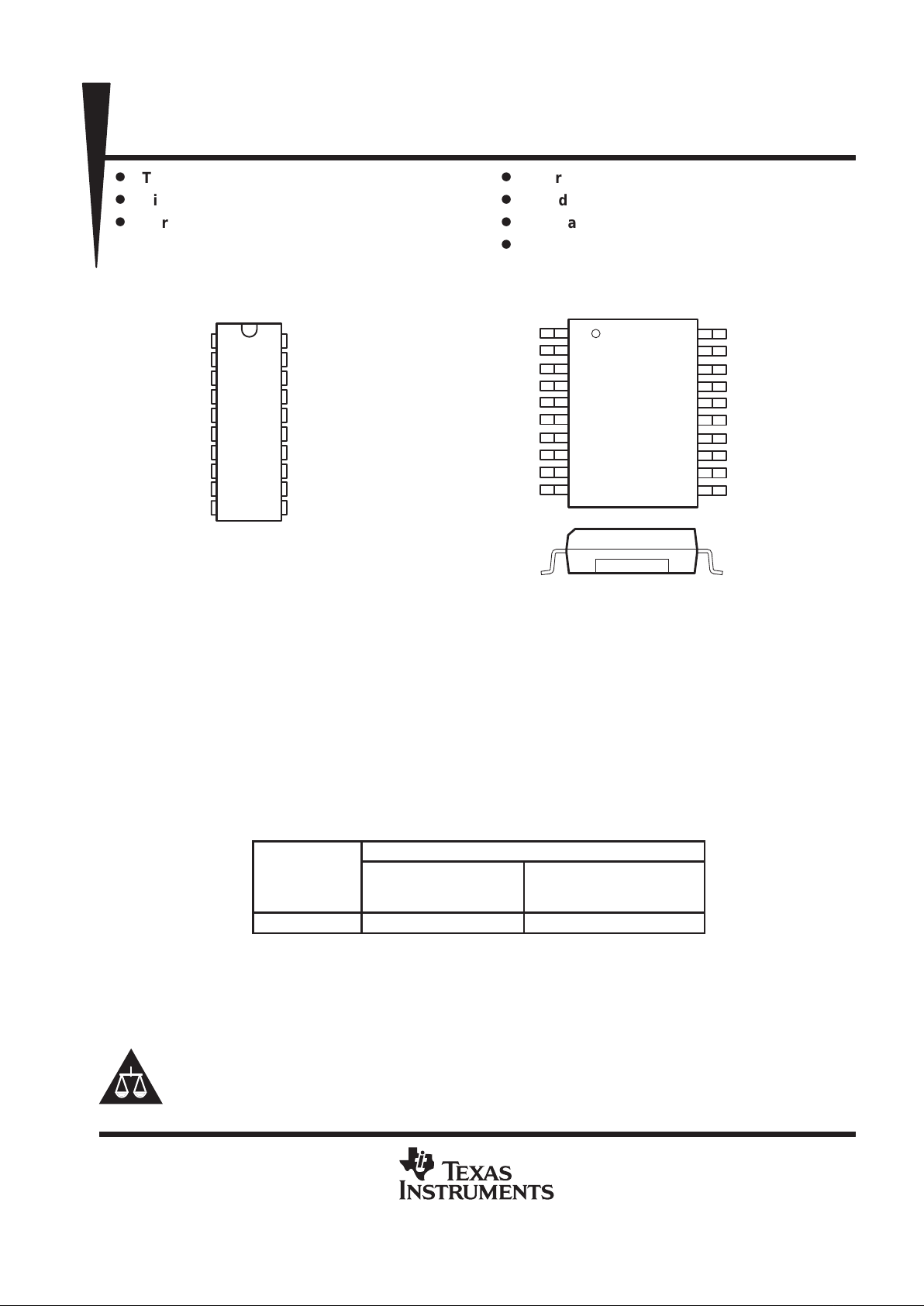
IN1
SGND
SVRR
OUT1
PGND
OUT2
V
CC
M/SB
IN2
GND/HS
GND/HS
GND/HS
GND/HS
GND/HS
GND/HS
GND/HS
GND/HS
GND/HS
GND/HS
GND/HS
NE PACKAGE
(TOP VIEW)
1
2
3
4
5
6
7
8
9
10
20
19
18
17
16
15
14
13
12
11
GND/HS
IN1
NC
SGND
SVRR
NC
OUT1
OUT1
PGND
GND/HS
GND/HS
IN2
NC
M/SB
V
CC
NC
OUT2
OUT2
PGND
GND/HS
DWP PACKAGE
(TOP VIEW)
Cross Section View Showing PowerPAD
NC – No internal connection
description
The TP A1517 is a stereo audio power amplifier that contains two identical amplifiers capable of delivering 6 W
per channel of continuous average power into a 4-Ω load at 10% THD+N or 5 W per channel at 1% THD+N.
The gain of each channel is fixed at 20 dB. The amplifier features a mute/standby function for power-sensitive
applications. The amplifier is available in Texas Instruments patented PowerPAD 20-pin surface-mount
thermally-enhanced package (DWP) that reduces board space and facilitates automated assembly while
maintaining exceptional thermal characteristics. It is also available in the 20-pin thermally enhanced DIP
package (NE).
AVAILABLE OPTIONS
PACKAGED DEVICES
T
A
THERMALLY ENHANCED
PLASTIC DIP
THERMALLY† ENHANCED
SURFACE MOUNT
(DWP)
–40°C to 85°C TPA1517NE TPA1517DWP
†
The DWP package is available taped and reeled. To order a taped and reeled part,
add the suffix R (e.g., TPA1517DWPR).
PRODUCTION DATA information is current as of publication date.
Products conform to specifications per the terms of Texas Instruments
standard warranty. Production processing does not necessarily include
testing of all parameters.
Copyright 2000, Texas Instruments Incorporated
Please be aware that an important notice concerning availability, standard warranty, and use in critical applications of
Texas Instruments semiconductor products and disclaimers thereto appears at the end of this data sheet.
PowerPAD is a trademark of Texas Instruments Incorporated.
TPA1517
6-W STEREO AUDIO POWER AMPLIFIER
SLOS162B – MARCH 1997 – REVISED MARCH 2000
2
POST OFFICE BOX 655303 • DALLAS, TEXAS 75265
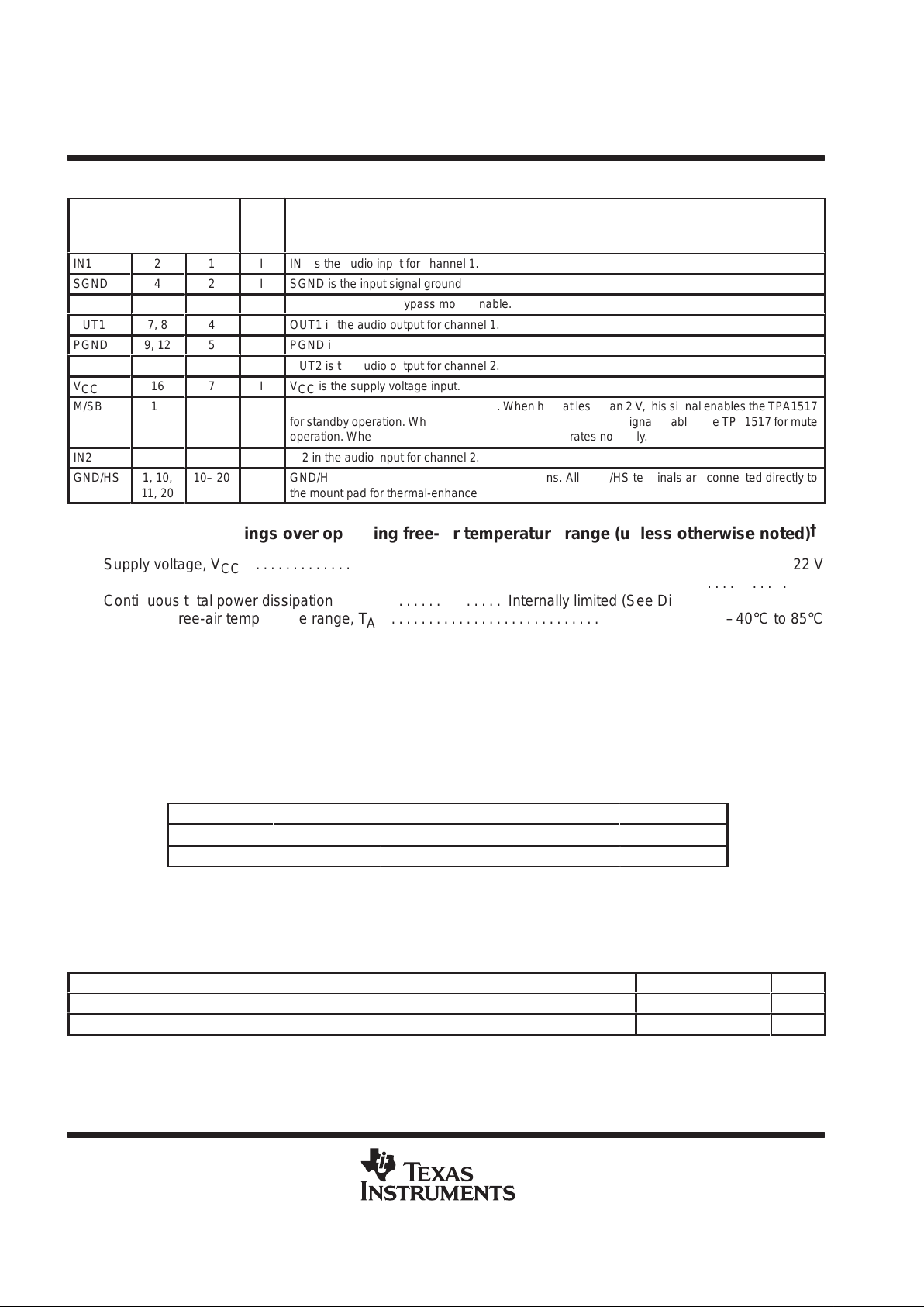
Terminal Functions
TERMINAL
NAME DWP
NO.
NE
NO.
I/O
DESCRIPTION
IN1
2
1
I
IN1 is the audio input for channel 1.
SGND
4
2
I
SGND is the input signal ground reference.
SVRR
5
3
SVRR is the midrail bypass mode enable.
OUT1
7, 8
4
O
OUT1 is the audio output for channel 1.
PGND
9, 12
5
PGND is the power ground reference.
OUT2
13, 14
6
O
OUT2 is the audio output for channel 2.
V
CC
16
7
I
VCC is the supply voltage input.
ÁÁ
Á
M/SB
Á
Á
17
ÁÁ
Á
8
Á
Á
I
ББББББББББББББББББББББ
Á
M/SB is the mute/standby mode enable. When held at less than 2 V , this signal enables the TP A1517
for standby operation. When held between 3.4 V and 8.8 V , this signal enables the TP A1517 for mute
operation. When held above 9.2 V, the TPA1517 operates normally.
IN2
19
9
I
IN2 in the audio input for channel 2.
ÁÁ
Á
GND/HS
Á
Á
1, 10,
11, 20
ÁÁ
Á
10– 20
ÁÁББББББББББББББББББББББ
Á
GND/HS are the ground and heatsink connections. All GND/HS terminals are connected directly to
the mount pad for thermal-enhanced operation.
absolute maximum ratings over operating free-air temperature range (unless otherwise noted)
†
Supply voltage, VCC 22 V. . . . . . . . . . . . . . . . . . . . . . . . . . . . . . . . . . . . . . . . . . . . . . . . . . . . . . . . . . . . . . . . . . . . . . .
Input voltage, VI (IN1, IN2) 22 V. . . . . . . . . . . . . . . . . . . . . . . . . . . . . . . . . . . . . . . . . . . . . . . . . . . . . . . . . . . . . . . . . .
Continuous total power dissipation Internally limited (See Dissipation Rating Table). . . . . . . . . . . . . . . . . . . . .
Operating free-air temperature range, TA –40°C to 85°C. . . . . . . . . . . . . . . . . . . . . . . . . . . . . . . . . . . . . . . . . . . .
Operating junction temperature range, TJ –40°C to 150°C. . . . . . . . . . . . . . . . . . . . . . . . . . . . . . . . . . . . . . . . . . .
Storage temperature range, T
stg
–65°C to 150°C. . . . . . . . . . . . . . . . . . . . . . . . . . . . . . . . . . . . . . . . . . . . . . . . . . .
Lead temperature 1,6 mm (1/16 inch) from case for 10 seconds: DWP or NE package 260°C. . . . . . . . . . . .
†
Stresses beyond those listed under “absolute maximum ratings” may cause permanent damage to the device. These are stress ratings only, and
functional operation of the device at these or any other conditions beyond those indicated under “recommended operating conditions” is not
implied. Exposure to absolute-maximum-rated conditions for extended periods may affect device reliability.
NOTE 1: These devices have been classified as Class 1 ESD sensitive products per MIL-PRF-38535 Method 3015.7. Appropriate precautions
should be taken to prevent serious damage to the device.
DISSIPATION RATING TABLE
PACKAGE
TA ≤ 25°C
DERATING FACTOR TA = 70°C TA = 85°C
DWP
‡
2.94 W
23.5 mW/°C
1.88 W
1.53 W
NE
‡
2.85 W
22.8 mW/°C 1.82 W 1.48 W
‡
See the Texas Instruments document,
PowerPAD Thermally Enhanced Package Application Report
(literature number SLMA002), for more information on the PowerPAD package. The thermal data was
measured on a PCB layout based on the information in the section entitled
Texas Instruments
Recommended Board for PowerPAD
on page 33 of the before mentioned document.
recommended operating conditions
MIN NOM MAX UNIT
Supply voltage, V
CC
9.5
18
V
Operating free-air temperature, T
A
–40
85
°C
TPA1517
6-W STEREO AUDIO POWER AMPLIFIER
SLOS162B – MARCH 1997 – REVISED MARCH 2000
3
POST OFFICE BOX 655303 • DALLAS, TEXAS 75265
electrical characteristics, VCC = 12 V, TA = 25°C (unless otherwise noted)
PARAMETER TEST CONDITIONS
MIN TYP MAX UNIT
I
CC
БББББББББББББББББ
Supply current
45
70
mA
V
O(DC)
DC output voltage See Note 2 4 V
V
(M/SB)
M/SB on voltage 9.5 V
V
O(M)
Mute output voltage VI = 1 V (max) 2 mV
I
CC(SB)
Supply current in standby mode 7 100 µA
NOTE 2: At 6 V < VCC < 18 V the DC output voltage is approximately VCC/2.
electrical characteristics, VCC = 14.5 V, TA = 25°C (unless otherwise noted)
PARAMETER TEST CONDITIONS
MIN TYP MAX UNIT
I
CC
БББББББББББББББББ
Supply current
50
80
mA
V
O(DC)
DC output voltage See Note 2 5 V
V
(M/SB)
Voltage on M/SB terminal for normal operation 9.5 V
V
O(M)
Mute output voltage VI = 1 V (max) 2 mV
I
CC(SB)
Supply current in standby mode 7 100 µA
NOTE 2: At 6 V < VCC < 18 V the DC output voltage is approximately VCC/2.
operating characteristic, V
CC
= 12 V, R
L
= 4 Ω, f = 1 kHz, TA = 25°C
PARAMETER TEST CONDITIONS
MIN TYP MAX UNIT
p
p
THD = 0.2%
3
POOutput power (see Note 3)
THD = 10%
6
W
SNR Signal-to-noise ratio 84 dB
THD Total harmonic distortion PO = 1 W, RL = 8 Ω, f = 1 kHz 0.1%
I
O(SM)
Non-repetitive peak output current
4
A
I
O(RM)
Repetitive peak output current
2.5
A
Low-frequency roll-off
–3 dB
45
Hz
High-frequency roll-off
–1 dB
20
kHz
Supply ripple rejection ratio
M/SB = On, f = 1 kHz
65
dB
Z
I
Input impedance
60
kΩ
Rs = 0,
M/SB = On
50
µV(rms)
V
n
Noise output voltage (see Note 4)
Rs = 10 kΩ,
M/SB = On
70
µV(rms)
M/SB = Mute
50
µV(rms)
Channel separation
Rs = 10 kΩ
58
dB
Gain 18.5 20 21
Channel balance
0.1
1
dB
NOTES: 3. Output power is measured at the output terminals of the IC.
4. Noise voltage is measured in a bandwidth of 20 Hz to 20 kHz.
TPA1517
6-W STEREO AUDIO POWER AMPLIFIER
SLOS162B – MARCH 1997 – REVISED MARCH 2000
4
POST OFFICE BOX 655303 • DALLAS, TEXAS 75265
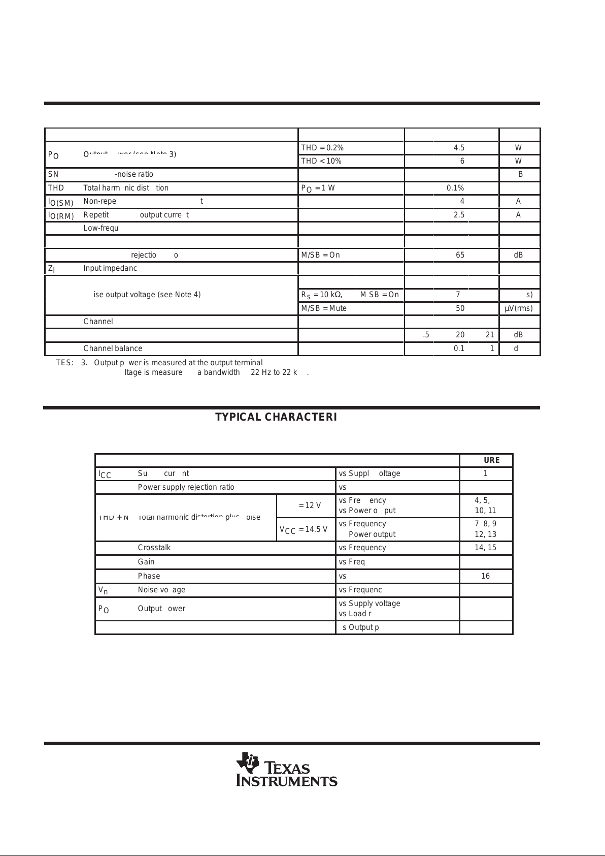
operating characteristic, V
CC
= 14.5 V, RL = 4 Ω, f = 1 kHz, TA = 25°C
PARAMETER TEST CONDITIONS
MIN TYP MAX UNIT
p
p
THD = 0.2%
4.5
W
POOutput power (see Note 3)
THD < 10%
6
W
SNR Signal-to-noise ratio 84 dB
THD Total harmonic distortion PO = 1 W 0.1%
I
O(SM)
Non-repetitive peak output current
4
A
I
O(RM)
Repetitive peak output current
2.5
A
Low-frequency roll-off
–3 dB
45
Hz
High-frequency roll-off
–1 dB
20
kHz
Supply ripple rejection ratio
M/SB = On
65
dB
Z
I
Input impedance
60
kΩ
Rs = 0,
M/SB = On
50
µV(rms)
V
n
Noise output voltage (see Note 4)
Rs = 10 kΩ,
M/SB = On
70
µV(rms)
M/SB = Mute
50
µV(rms)
Channel separation
Rs = 10 kΩ
58
dB
Gain 18.5 20 21 dB
Channel balance
0.1
1
dB
NOTES: 3. Output power is measured at the output terminals of the IC.
4. Noise voltage is measured in a bandwidth of 22 Hz to 22 kHz.
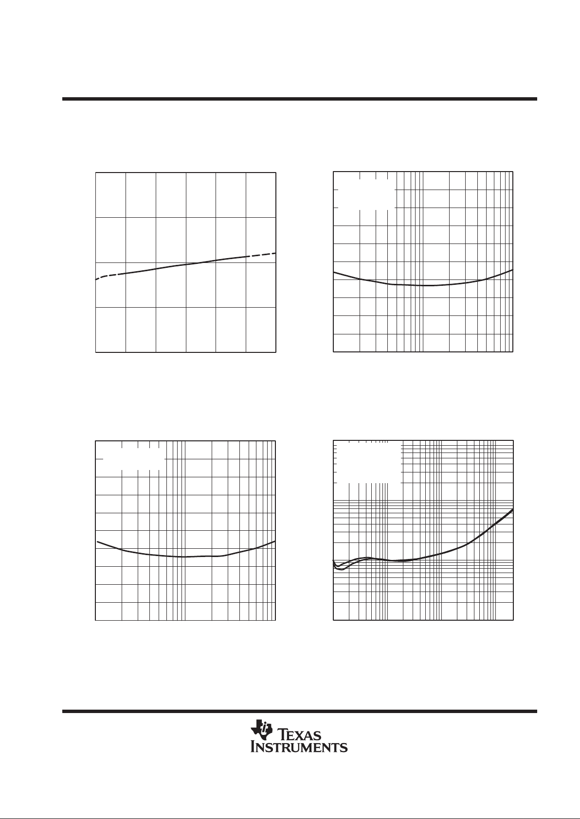
TYPICAL CHARACTERISTICS
Table of Graphs
FIGURE
I
CC
Supply current vs Supply voltage 1
Power supply rejection ratio vs Frequency 2, 3
p
VCC = 12 V
vs Frequency
vs Power output
4, 5, 6
10, 11
THD
+
N
Total harmonic distortion plus noise
VCC = 14.5 V
vs Frequency
vs Power output
7, 8, 9
12, 13
Crosstalk vs Frequency 14, 15
Gain vs Frequency 16
Phase vs Frequency 16
V
n
Noise voltage vs Frequency 17, 18
P
O
Output power
vs Supply voltage
vs Load resistance
19
20
P
D
Power dissipation vs Output power 21, 22
TPA1517
6-W STEREO AUDIO POWER AMPLIFIER
SLOS162B – MARCH 1997 – REVISED MARCH 2000
5
POST OFFICE BOX 655303 • DALLAS, TEXAS 75265
TYPICAL CHARACTERISTICS
Figure 1
50
0
81012
– Supply Current – mA
SUPPLY CURRENT
vs
SUPPLY VOLTAGE
100
14 16 18 20
I
CC
VCC – Supply Voltage – V
25
75
Figure 2
– 50
– 60
– 80
– 90
– 100
0
– 70
100 1 k 10 k
Supply Ripple Rejection Ratio – dB
– 30
– 40
– 20
f – Frequency – Hz
SUPPLY RIPPLE REJECTION RATIO
vs
FREQUENCY
– 10
VCC = 12 V
RL = 4 Ω
CB = 100 µF
Figure 3
– 50
– 60
– 80
– 100
100 1 k
– 30
– 10
SUPPLY RIPPLE REJECTION RATIO
vs
FREQUENCY
0
10 K
– 20
– 40
– 70
– 90
VCC = 14.5 V
RL = 4 Ω
f – Frequency – Hz
Supply Ripple Rejection Ratio – dB
Figure 4
0.1%
0.01%
20 100
THD+N – Total Harmonic Distortion + Noise
1%
f – Frequency – Hz
TOTAL HARMONIC DISTORTION PLUS NOISE
vs
FREQUENCY
10%
1 k 10 k 20 k
VCC = 12 V
RL = 4 Ω
PO = 3 W
Both Channels
TPA1517
6-W STEREO AUDIO POWER AMPLIFIER
SLOS162B – MARCH 1997 – REVISED MARCH 2000
6
POST OFFICE BOX 655303 • DALLAS, TEXAS 75265
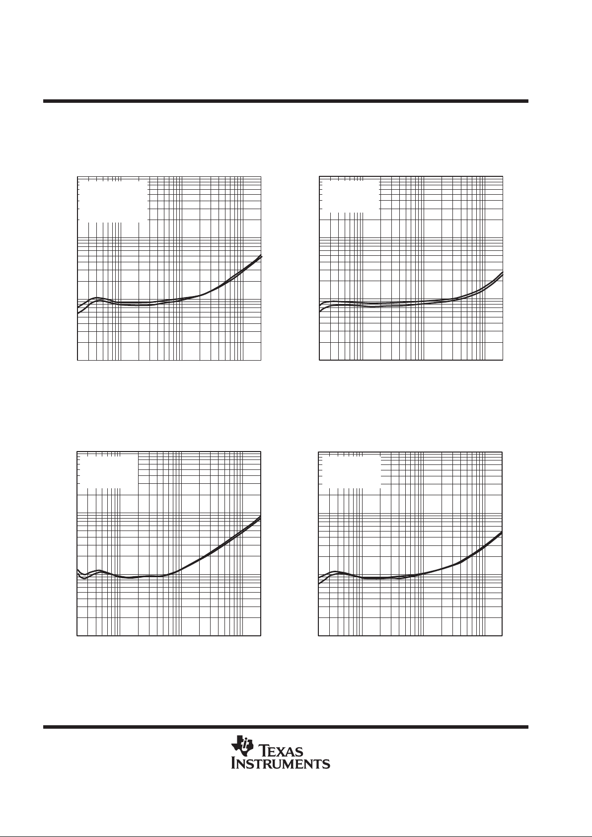
TYPICAL CHARACTERISTICS
Figure 5
0.1%
0.01%
20 100 1 k
THD+N – Total Harmonic Distortion + Noise
1%
f – Frequency – Hz
TOTAL HARMONIC DISTORTION PLUS NOISE
vs
FREQUENCY
10%
10 k 20 k
VCC = 12 V
RL = 8 Ω
PO = 1 W
Both Channels
Figure 6
20
0.1%
0.01%
100 1 k
THD+N – Total Harmonic Distortion + Noise
1%
f – Frequency – Hz
TOTAL HARMONIC DISTORTION PLUS NOISE
vs
FREQUENCY
10%
10 k 20 k
VCC = 12 V
RL = 32 Ω
PO = 0.25 W
Figure 7
20
0.1%
0.01%
100 1 k
THD+N – Total Harmonic Distortion + Noise
1%
f – Frequency – Hz
TOTAL HARMONIC DISTORTION PLUS NOISE
vs
FREQUENCY
10%
10 k 20 k
VCC = 14.5 V
RL = 4 Ω
PO = 3 W
Figure 8
20
0.1%
0.01%
100 1 k
THD+N – Total Harmonic Distortion + Noise
1%
f – Frequency – Hz
TOTAL HARMONIC DISTORTION PLUS NOISE
vs
FREQUENCY
10%
10 k 20 k
VCC = 14.5 V
RL = 8 Ω
PO = 1.5 W

TPA1517
6-W STEREO AUDIO POWER AMPLIFIER
SLOS162B – MARCH 1997 – REVISED MARCH 2000
7
POST OFFICE BOX 655303 • DALLAS, TEXAS 75265
TYPICAL CHARACTERISTICS
Figure 9
20
0.1%
0.01%
100 1 k
THD+N – Total Harmonic Distortion + Noise
1%
f – Frequency – Hz
TOTAL HARMONIC DISTORTION PLUS NOISE
vs
FREQUENCY
10%
10 k 20 k
VCC = 14.5 V
RL = 32 Ω
PO = 0.25 W
Figure 10
PO – Power Output – W
0.01 0.1 1 10
0.1%
0.01%
THD+N – Total Harmonic Distortion + Noise
1%
TOTAL HARMONIC DISTORTION PLUS NOISE
vs
POWER OUTPUT
10%
VCC = 12 V
RL = 4 Ω
Both Channels
f = 20 Hz
f = 20 kHz
f = 1 kHz
Figure 11
PO – Power Output – W
0.01 0.1 1 10
0.1%
0.01%
THD+N – Total Harmonic Distortion + Noise
1%
TOTAL HARMONIC DISTORTION PLUS NOISE
vs
POWER OUTPUT
10%
VCC = 12 V
RL = 8 Ω
Both Channels
f = 20 Hz
f = 20 kHz
f = 1 kHz
Figure 12
PO – Power Output – W
0.01 0.1 1 10
0.1%
0.01%
THD+N – Total Harmonic Distortion + Noise
1%
TOTAL HARMONIC DISTORTION PLUS NOISE
vs
POWER OUTPUT
10%
VCC = 14.5 V
RL = 4 Ω
Both Channels
f = 20 Hz
f = 20 kHz
f = 1 kHz

TPA1517
6-W STEREO AUDIO POWER AMPLIFIER
SLOS162B – MARCH 1997 – REVISED MARCH 2000
8
POST OFFICE BOX 655303 • DALLAS, TEXAS 75265
TYPICAL CHARACTERISTICS
Figure 13
PO – Power Output – W
0.01 0.1 1 10
0.1%
0.01%
THD+N – Total Harmonic Distortion + Noise
1%
TOTAL HARMONIC DISTORTION PLUS NOISE
vs
POWER OUTPUT
10%
VCC = 14.5 V
RL = 8 Ω
Both Channels
f = 20 kHz
f = 20 Hz
f = 1 kHz
Figure 14
– 60
– 65
– 70
– 80
20 100 1 k
Crosstalk – dB
– 50
– 45
f – Frequency – Hz
CROSSTALK
vs
FREQUENCY
– 40
10 k 20 k
– 55
– 75
VCC = 12 V
RL = 4 Ω
PO = 3 W
Both Channels
– 60
– 65
– 70
– 80
20 100 1 k
Crosstalk – dB
– 50
– 45
f – Frequency – Hz
CROSSTALK
vs
FREQUENCY
– 40
10 k 20 k
– 55
– 75
VCC = 14.5 V
RL = 4 Ω
PO = 5 W
Both Channels
Figure 15

TPA1517
6-W STEREO AUDIO POWER AMPLIFIER
SLOS162B – MARCH 1997 – REVISED MARCH 2000
9
POST OFFICE BOX 655303 • DALLAS, TEXAS 75265
TYPICAL CHARACTERISTICS
– 10
– 20
– 30
– 40
10 100 1 k 10 k
Gain – dB
0
10
f – Frequency – Hz
GAIN AND PHASE
vs
FREQUENCY
20
100 k 1 M
200°
100°
0°
–100°
–200°
VCC = 12 V
RL = 4 Ω
Phase
Phase
Gain
Figure 16
Figure 17
20 100 1 k
f – Frequency – Hz
NOISE VOLTAGE
vs
FREQUENCY
10 k 20 k
VCC = 12 V
BW = 22 Hz to 22 kHz
RL = 4 Ω
Both Channels
1
0.1
0.01
– Noise Voltage – mV
V
n
Figure 18
20 100 1 k
f – Frequency – Hz
NOISE VOLTAGE
vs
FREQUENCY
10 k 20 k
VCC = 14.5 V
BW = 22 Hz to 22 kHz
RL = 4 Ω
Both Channels
1
0.1
0.01
– Noise Voltage – mV
V
n

TPA1517
6-W STEREO AUDIO POWER AMPLIFIER
SLOS162B – MARCH 1997 – REVISED MARCH 2000
10
POST OFFICE BOX 655303 • DALLAS, TEXAS 75265
TYPICAL CHARACTERISTICS
Figure 19
VCC – Supply Voltage – V
4
2
0
8 9 10 11 12 13 14
6
8
15 16 17 18
RL = 4 Ω
RL = 8 Ω
OUTPUT POWER
vs
SUPPLY VOLTAGE
– Output Power – WP
O
THD < 1%
Figure 20
VCC = 14.5 V
VCC = 12 V
THD < 1%
3
2
1
0
2 4 6 8 14 16 20
4
5
OUTPUT POWER
vs
LOAD RESISTANCE
6
22 24 28 3210 12 18 26 30
RL – Load Resistance – Ω
– Output Power – WP
O
Figure 21
2
1.5
1
0.5
0123
2.5
3
POWER DISSIPATION
vs
OUTPUT POWER
3.5
456
VCC = 12 V
RL = 4 Ω
RL = 8 Ω
PO – Output Power – W
– Power Dissipation – WP
D
Figure 22
2
1.5
1
0.5
0123
2.5
3
POWER DISSIPATION
vs
OUTPUT POWER
3.5
456
VCC = 14.5 V
RL = 4 Ω
PO – Output Power – W
RL = 8 Ω
– Power Dissipation – WP
D

TPA1517
6-W STEREO AUDIO POWER AMPLIFIER
SLOS162B – MARCH 1997 – REVISED MARCH 2000
11
POST OFFICE BOX 655303 • DALLAS, TEXAS 75265
APPLICATION INFORMATION
amplifier operation
The TPA1517 is a stereo audio power amplifier designed to drive 4-Ω speakers at up to 6 W per channel.
Figure 23 is a schematic diagram of the minimum recommended configuration of the amplifier. Gain is internally
fixed at 20 dB (gain of 10 V/V).
Mute
Standby
C
B
V
CC
IN2
SGND
PGND
IN11
C
IR
Right
Ref
Left
Mute/Standby Select
(see Note B)
C
OR
C
OL
SVRR
OUT1
M/SB
OUT2
2
5
3
9
10 kΩ
6.8 kΩ
V
CC
2 kΩ
2 kΩ
18 kΩ
18 kΩ
GND/HS
4
8
6
10 – 20
Copper Plane
Mute/Standby Switch
(see Note A)
C
S
V
CC
V
CC
7
+
+
–
OUT2
+
+
–
+
–
60 k
2.1 V
ref
+
–
2.1 V
ref
× 1
× 1
60 k
× 1
15 kΩ
15 kΩ
C
IL
S1
S2
1 µF
470 µF
470 µF
1 µF
1 µF
2.2 µF
NOTES: A. When S1 is open, the TPA1517 operates normally. When this switch is closed, the device is in mute/standby mode.
B. When S2 is open, activating S1 places the TPA1517 in mute mode. When S2 is closed, activating S1 places the TP A1517 in standby
mode.
C. The terminal numbers are for the 20-pin NE package.
Figure 23. TPA1517 Minimum Configuration
The following equation is used to relate gain in V/V to dB:
G
dB
+
20 LOGǒG
VńV
Ǔ

TPA1517
6-W STEREO AUDIO POWER AMPLIFIER
SLOS162B – MARCH 1997 – REVISED MARCH 2000
12
POST OFFICE BOX 655303 • DALLAS, TEXAS 75265
APPLICATION INFORMATION
The audio outputs are biased to a midrail voltage which is shown by the following equation:
V
MID
+
V
CC
2
The audio inputs are always biased to 2.1 V when in mute or normal mode. Any dc offset between the input signal
source and the input terminal is amplified and can seriously degrade the performance of the amplifier. For this
reason, it is recommended that the inputs always be connected through a series capacitor (ac coupled). The
power outputs, also having a dc bias, must be connected to the speakers via series capacitors.
mute/standby operation
The TP A1517 has three modes of operation; normal, mute, and standby . They are controlled by the voltage on
the M/SB terminal as described in Figure 24. In normal mode, the TP A1517 amplifies the signal applied to the
two input terminals providing low impedance drive to speakers connected to the output terminals. In mute mode,
the amplifier retains all bias voltages and quiescent supply current levels but does not pass the input signal to
the output. In standby mode, the internal bias generators and power-drive stages are turned off, thereby
reducing the supply current levels.
NORMAL
MUTE
STANDBY
Undetermined State
Undetermined State
22
9.2
8.8
3.4
2
0
– Input Voltage on M/SB – V
V
I(M/SB)
Figure 24. Standby, Mute, and Normal (On) Operating Conditions
The designer must take care to place the control voltages within the defined ranges for each desired mode,
whenever an external circuit is used to control the input voltage at the M/SB terminal. The undefined area can
cause unpredictable performance and should be avoided. As the control voltage moves through the undefined
areas pop or click sounds may be heard in the speaker. Moving from mute to normal causes a very small click
sound. Whereas moving from standby to mute can cause a much larger pop sound. Figure 25 shows external
circuitry designed to help reduce transition pops when moving from standby mode to normal mode.

TPA1517
6-W STEREO AUDIO POWER AMPLIFIER
SLOS162B – MARCH 1997 – REVISED MARCH 2000
13
POST OFFICE BOX 655303 • DALLAS, TEXAS 75265
APPLICATION INFORMATION
Figure 25 is a reference schematic that provides TTL-level control of the M/SB terminal. A diode network is also
included which helps reduce turn-on pop noises. The diodes serve to drain the charge out of the output coupling
capacitors while the amplifier is in shutdown mode. When the M/SB voltage is in the normal operating range,
the diodes have no effect on the ac performance of the system.
Mute
Standby
C
B
V
CC
IN2
SGND
PGND
IN11
C
IR
Right
Ref
Left
C
OR
C
OL
SVRR
OUT1
M/SB
OUT2
2
5
3
9
2 kΩ
2 kΩ
18 kΩ
18 kΩ
GND/HS
4
8
6
10 – 20
Copper Plane
C
S
V
CC
V
CC
7
+
+
–
OUT2
+
+
–
+
–
60 k
2.1 V
ref
+
–
2.1 V
ref
× 1
× 1
60 k
× 1
15 kΩ
15 kΩ
C
IL
S2
See
Note B
1N914
10 kΩ
6.8 kΩ
10 kΩ
47 kΩ
10 kΩ
47 kΩ
47 kΩ
V
CC
TTL Control
Low – Mute
High – On
S1
See
Note A
220 Ω
Q1
Q2
1 µF
470 µF
1N914
470 µF
1 µF
1 µF
2.2 µF
NOTES: A. When S1 is closed, the depop circuitry is active during standby mode.
B. When S2 is open, activating S1 places the TPA1517 in mute mode. When S2 is closed, activating S1 places the TP A1517 in standby
mode.
C. The terminal numbers are for the 20-pin NE package.
Figure 25. TTL Control with POP Reduction

TPA1517
6-W STEREO AUDIO POWER AMPLIFIER
SLOS162B – MARCH 1997 – REVISED MARCH 2000
14
POST OFFICE BOX 655303 • DALLAS, TEXAS 75265
APPLICATION INFORMATION
component selection
Some of the general concerns for selection of capacitors are:
D
Leakage currents on aluminum electrolytic capacitors
D
ESR (equivalent series resistance)
D
Temperature ratings
leakage currents
Leakage currents on most ceramic, polystyrene, and paper capacitors are negligible for this application.
Leakage currents for aluminum electrolytic and tantalum tend to be higher. This is especially important on the
input terminals and the SVRR capacitor. These nodes encounter from 3 V to 7 V, and need to have leakage
currents less than 1 µA to keep from affecting the output power and noise performance.
equivalent series resistance
ESR is mainly important on the output coupling capacitor , where even 1 Ω of ESR in C
O
with an 8-Ω speaker
can reduce the output drive power by 12.5%. ESR should be considered across the frequency range of interest,
(i.e., 20 Hz to 20 kHz). The following equation calculates the amount of power lost in the coupling capacitor:
% Power in C
O
+
ESR
R
L
In general, the power supply decoupling requires a very low ESR as well to take advantage of the full output
drive current.
temperature range
The temperature range of the capacitors may or may not seem like an obvious thing to specify, but it is very
important. Many of the high-density capacitors perform very differently at different temperatures. When
consistent high performance is required from the system over temperature in terms of low THD, maximum
output power, and turn-on/off popping, then interactions of the coupling capacitors and the SVRR capacitors
need to be considered, as well as the change in ESR on the output capacitor with temperature.
turn-on pop consideration
To select the proper input coupling capacitor, the designer should select a capacitor large enough to allow the
lowest desired frequency pass and small enough that the time constant is shorter than the output RC time
constant to minimize turn-on popping. The input time constant for the TPA1517 is determined by the input
60-kΩ resistance of the amplifier, and the input coupling capacitor according to the following generic equation:
TC+
1
2pRC
For example, 8-Ω speakers and 220-µF output coupling capacitors would yield a 90-Hz cut-off point for the
output RC network. The input network should be the same speed or faster ( > 90 Hz TC). A good choice would
be 180 Hz. As the input resistance is 60 kΩ, a 14-nF input coupling capacitor would do.
The bypass-capacitor time constant should be much larger (×5) than either the input coupling capacitor time
constant or the output coupling capacitor time constants. In the previous example with the 220-µF output
coupling capacitor, the designer should want the bypass capacitor, T
C
, to be in the order of 18 Hz or lower. To
get an 18-Hz time constant, CB is required to be 1 µF or larger because the resistance this capacitor sees is
7.5 kΩ.

TPA1517
6-W STEREO AUDIO POWER AMPLIFIER
SLOS162B – MARCH 1997 – REVISED MARCH 2000
15
POST OFFICE BOX 655303 • DALLAS, TEXAS 75265
APPLICATION INFORMATION
In summary , follow one of the three simple relations presented below , depending on the tradeoffs between low
frequency response and turn-on pop. If depop performance is the top priority, then follow:
7500 CBu
5RLCOu
300000 C
I
If low frequency ac response is more important but depop is still a consideration then follow:
1
2p60000 C
I
t
10 Hz
Finally, if low frequency response is most important and depop is not a consideration then follow:
1
2p60000 C
I
≤
1
2pRLC
I
≤ f
low
thermal applications
Linear power amplifiers dissipate a significant amount of heat in the package under normal operating conditions.
A typical music CD requires 12 dB to 15 dB of dynamic headroom to pass the loudest portions without distortion
as compared with the average power output. Figure 19 shows that when the TP A1517 is operating from a 12-V
supply into a 4-Ω speaker that approximately 3.5 W peaks are possible. Converting watts to dB using the
following equation:
P
dB
+
10Log
ǒ
P
W
P
ref
Ǔ
+
10Log
ǒ
3.5
1
Ǔ
+
5.44 dB
Subtracting dB for the headroom restriction to obtain the average listening level without distortion yields the
following:
5.44 dB*15 dB
+*
9.56 dB(15 dB headroom
)
5.44 dB*12 dB
+*
6.56 dB(12 dB headroom
)
Converting dB back into watts:
P
W
+
10
PdBń
10
P
ref
+
111 mW (15 dB headroom)
+
221 mW (12 dB headroom)
This is valuable information to consider when attempting to estimate the heat dissipation requirements for the
amplifier system. Comparing the absolute worst cast, which is 3.5 W of continuous power output with 0 dB of
headroom, against 12-dB and 15-dB applications drastically affects maximum ambient temperature ratings for
the system. Using the power dissipation curves for a 12-V , 4-Ω system, internal dissipation in the TP A1517 and
maximum ambient temperatures are shown in Table 1.

TPA1517
6-W STEREO AUDIO POWER AMPLIFIER
SLOS162B – MARCH 1997 – REVISED MARCH 2000
16
POST OFFICE BOX 655303 • DALLAS, TEXAS 75265
APPLICATION INFORMATION
Table 1. TPA1517 Power Rating
PEAK OUTPUT POWER
POWER DISSIPATION MAXIMUM AMBIENT
(W)
AVERAGE OUTPUT POWER
(W/Channel) TEMPERATURE
3.5 3.5 W 2.1 –34°C
3.5 1.77 W (3 dB) 2.4 –61°C
3.5 884 mW (6 dB) 2.25 –48°C
3.5 442 mW (9 dB) 1.75 –4°C
3.5 221 mW (12 dB) 1.5 18°C
3.5 111 mW (15 dB) 1.25 40°C
The maximum ambient temperature depends on the heatsinking ability of the PCB system. Using the derating
factor for the NE package with 4 square inches of copper area is 22.8 mW/°C and 38.8 mW/°C respectively.
Converting this to θ
JA
:
θ
JA
+
1
Derating
+
1
0.0228
+
43.9°CńW
For 0 CFM :
To calculate maximum ambient temperatures, first consider that the numbers from the dissipation graphs are
per channel so the dissipated heat needs to be doubled for two channel operation. Given θ
JA
, the maximum
allowable junction temperature and the total internal dissipation, the maximum ambient temperature can be
calculated with the following equation. The maximum recommended junction temperature for the TP A1517 is
150°C.
T
A
Max+TJMax*qJAP
D
+
150*43.9(1.25 2)+
40°C(15 dB headroom, 0 CFM
)
Table 1 clearly shows that for most applications some airflow is required to keep junction temperatures in the
specified range. The TPA1517 is designed with thermal protection that turns the device off when the junction
temperature surpasses 150°C to prevent damage to the IC. Using the DWP package on a multilayer PCB with
internal ground planes can achieve better thermal performance. T able 1 was calculated for a maximum volume
system; when the output level is reduced, the numbers in the table change significantly . Also using 8-Ω speakers
dramatically increases the thermal performance by increasing amplifier efficiency.

TPA1517
6-W STEREO AUDIO POWER AMPLIFIER
SLOS162B – MARCH 1997 – REVISED MARCH 2000
17
POST OFFICE BOX 655303 • DALLAS, TEXAS 75265
APPLICATION INFORMATION
60
30
10
0
0123456
– Theta JA –
70
80
TPA1517 NE THERMAL RESISTANCE, θ
JA
vs
COPPER AREA
90
78910
50
40
20
JA
θ
C/W
°
Copper Area – in
2
Figure 26

TPA1517
6-W STEREO AUDIO POWER AMPLIFIER
SLOS162B – MARCH 1997 – REVISED MARCH 2000
18
POST OFFICE BOX 655303 • DALLAS, TEXAS 75265
MECHANICAL INFORMATION
DWP (R-PDSO-G20) PowerPAD PLASTIC SMALL-OUTLINE PACKAGE
Gage Plane
0.411 (10,44)
0.430 (10,92)
0.010 (0,25) NOM
0.010 (0,25)
Seating Plane
0.050 (1,27)
0.016 (0,40)
4073226/B 01/96
11
10
0.500 (12,70)
0.510 (12,95)
20
1
0.004 (0,10)
0.000 (0,00)
0.096 (2,43) MAX
0.020 (0,51)
0.014 (0,35)
0.293 (7,45)
0.299 (7,59)
0.050 (1,27)
M
0.010 (0,25)
0.004 (0,10)
+2°–8°
Thermal Pad 0.150 (3,81) 0.170 (4,31) NOM
(see Note C)
NOTES: A. All linear dimensions are in inches (millimeters).
B. This drawing is subject to change without notice.
C. The thermal performance may be enhanced by bonding the thermal pad to an external thermal plane. This solderable pad is
electrically and thermally connected to the backside of the die and leads 1, 10, 11 and 20.
PowerPAD is a trademark of Texas Instruments Incorporated.

TPA1517
6-W STEREO AUDIO POWER AMPLIFIER
SLOS162B – MARCH 1997 – REVISED MARCH 2000
19
POST OFFICE BOX 655303 • DALLAS, TEXAS 75265
MECHANICAL INFORMATION
NE (R-PDIP-T**) PLASTIC DUAL-IN-LINE PACKAGE
20 PIN SHOWN
20
16
PINS **
0.780 (19,80)
0.240 (6,10)
0.260 (6,60)
Seating Plane
DIM
0.975 (24,77)
0.914 (23,22)
0.930 (23,62)
1.000 (25,40)
0.260 (6,61)
0.280 (7,11)
Seating Plane
0.010 (0,25) NOM
4040054/B 04/95
0.310 (7,87)
0.290 (7,37)
0.070 (1,78) MAX
C
10
0.021 (0,533)
0.015 (0,381)
A
11
1
20
0.015 (0,381)
0.021 (0,533)
B
0.200 (5,08) MAX
0.020 (0,51) MIN
0.125 (3,17)
0.155 (3,94)
0.020 (0,51) MIN
0.200 (5,08) MAX
0.155 (3,94)
0.125 (3,17)
M
0.010 (0,25)
M
0.010 (0,25)
0.100 (2,54)
0°–15°
0.100 (2,54)
C
B
A
MIN
MAX
MIN
MAX
MIN
MAX
NOTES: A. All linear dimensions are in inches (millimeters).
B. This drawing is subject to change without notice.
C. Falls within JEDEC MS-001 (16 pin only)

IMPORTANT NOTICE
T exas Instruments and its subsidiaries (TI) reserve the right to make changes to their products or to discontinue
any product or service without notice, and advise customers to obtain the latest version of relevant information
to verify, before placing orders, that information being relied on is current and complete. All products are sold
subject to the terms and conditions of sale supplied at the time of order acknowledgement, including those
pertaining to warranty, patent infringement, and limitation of liability.
TI warrants performance of its semiconductor products to the specifications applicable at the time of sale in
accordance with TI’s standard warranty. Testing and other quality control techniques are utilized to the extent
TI deems necessary to support this warranty. Specific testing of all parameters of each device is not necessarily
performed, except those mandated by government requirements.
CERT AIN APPLICATIONS USING SEMICONDUCTOR PRODUCTS MAY INVOLVE POTENTIAL RISKS OF
DEATH, PERSONAL INJURY, OR SEVERE PROPERTY OR ENVIRONMENTAL DAMAGE (“CRITICAL
APPLICATIONS”). TI SEMICONDUCTOR PRODUCTS ARE NOT DESIGNED, AUTHORIZED, OR
WARRANTED TO BE SUITABLE FOR USE IN LIFE-SUPPORT DEVICES OR SYSTEMS OR OTHER
CRITICAL APPLICATIONS. INCLUSION OF TI PRODUCTS IN SUCH APPLICA TIONS IS UNDERSTOOD T O
BE FULLY AT THE CUSTOMER’S RISK.
In order to minimize risks associated with the customer’s applications, adequate design and operating
safeguards must be provided by the customer to minimize inherent or procedural hazards.
TI assumes no liability for applications assistance or customer product design. TI does not warrant or represent
that any license, either express or implied, is granted under any patent right, copyright, mask work right, or other
intellectual property right of TI covering or relating to any combination, machine, or process in which such
semiconductor products or services might be or are used. TI’s publication of information regarding any third
party’s products or services does not constitute TI’s approval, warranty or endorsement thereof.
Copyright 2000, Texas Instruments Incorporated
 Loading...