

Page 1
www.ti.com
1
2
3
4
8
7
6
5
VO1
IN1–
IN1+
GND
V
DD
VO2
IN2–
IN2+
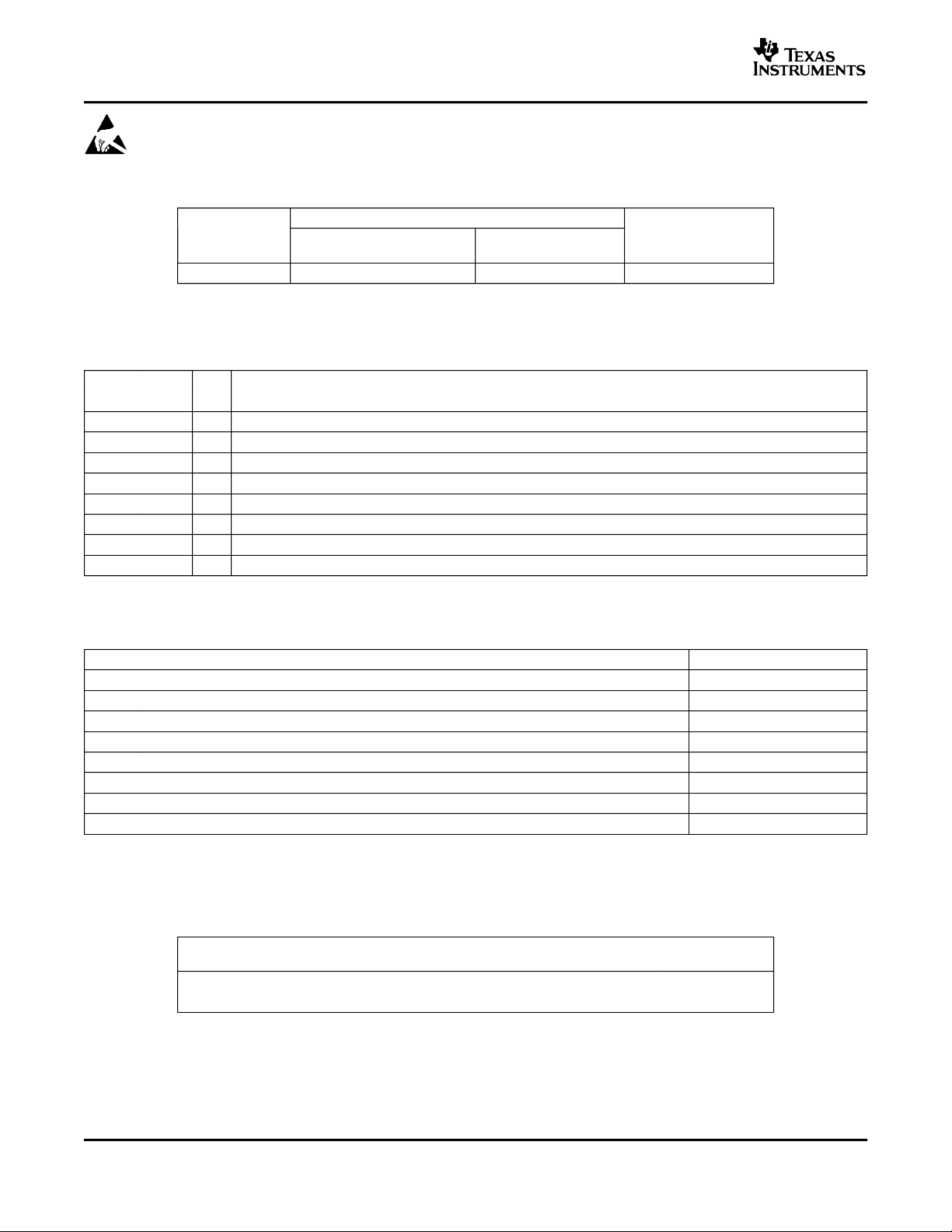
D OR DGN PACKAGE
(TOP VIEW)
Short-Circuit
Protection
Over-Temperature
Protection
V
DD
8
V
DD
IN1−
IN1+
IN2−
IN2+
2
3
6
5
VO1
1
VO2
7
4
R
F
R
F
R
F
R
I
R
I
R
I
R
I
V
DD/2
C
I
C
I
C
I
C
I
LIN−
LIN+
RIN−
RIN+
R
F
R
O
R
O
R
C
R
C
C
C
C
C
To Headphone
Jack
(See TPA152)
SLOS212E – AUGUST 1998 – REVISED JUNE 2004
150-mW STEREO AUDIO POWER AMPLIFIER
FEATURES DESCRIPTION
• 150-mW Stereo Output
• Wide Range of Supply Voltages
– Fully Specified for 3.3-V and 5-V Operation
– Operational From 2.5 V to 5.5 V
• Thermal and Short-Circuit Protection input channel and does not require external compen-
• Surface-Mount Packaging
– PowerPAD™ MSOP
– SOIC
• Standard Operational Amplifier Pinout
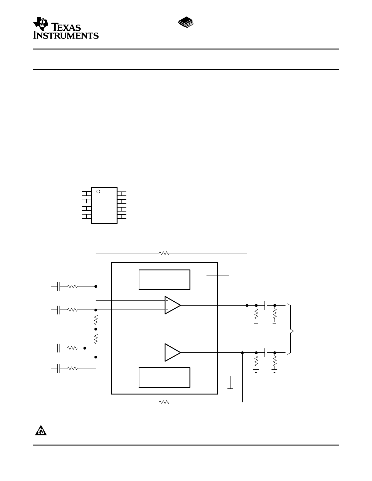
The TPA112 is a stereo audio power amplifier packaged in an 8-pin PowerPAD™ MSOP package
capable of delivering 150 mW of continuous RMS
power per channel into 8-Ω loads. Amplifier gain is
externally configured by means of two resistors per
sation for settings of 1 to 10.
THD+N when driving an 8-Ω load from 5 V is 0.1% at
1 kHz, and less than 2% across the audio band of 20
Hz to 20 kHz. For 32-Ω loads, the THD+N is reduced
to less than 0.06% at 1 kHz, and is less than 1%
across the audio band of 20 Hz to 20 kHz. For 10-kΩ
loads, the THD+N performance is 0.01% at 1 kHz,
and less than 0.02% across the audio band of 20 Hz
to 20 kHz.
TPA112
FUNCTIONAL BLOCK DIAGRAM
PRODUCTION DATA information is current as of publication date.
Products conform to specifications per the terms of the Texas
Instruments standard warranty. Production processing does not
necessarily include testing of all parameters.
PowerPAD is a trademark of Texas Instruments.
Please be aware that an important notice concerning availability, standard warranty, and use in critical applications of Texas
Instruments semiconductor products and disclaimers thereto appears at the end of this data sheet.
Copyright © 1998–2004, Texas Instruments Incorporated
Page 2
www.ti.com
TPA112
SLOS212E – AUGUST 1998 – REVISED JUNE 2004
These devices have limited built-in ESD protection. The leads should be shorted together or the device
placed in conductive foam during storage or handling to prevent electrostatic damage to the MOS gates.
AVAILABLE OPTIONS
PACKAGED DEVICES
T
A
SMALL OUTLINE
(D) (DGN)
–40°C to 85°C TPA112D TPA112DGN TI AAD
(1) The D and DGN packages are available in left-ended tape and reel only (e.g., TPA112DR,
TPA112DGNR).
TERMINAL
NAME NO.
I/O DESCRIPTION
GND 4 I GND is the ground connection.
IN1- 2 I IN1- is the inverting input for channel 1.
IN1+ 3 I IN1+ is the noninverting input for channel 1.
IN2- 6 I IN2- is the inverting input for channel 2.
IN2+ 5 I IN2+ is the noninverting input for channel 2.
V
DD
8 I V
is the supply voltage terminal.
DD
VO1 1 O VO1 is the audio output for channel 1.
VO2 7 O VO2 is the audio output for channel 2.
(1)
Terminal Functions
(1)
MSOP
MSOP
SYMBOLIZATION
ABSOLUTE MAXIMUM RATINGS
over operating free-air temperature range (unless otherwise noted)
V
V
I
I
I
O
T
T
(1) Stresses beyond those listed under "absolute maximum ratings” may cause permanent damage to the device. These are stress ratings
Supply voltage 6 V
DD
Differential input voltage –0.3 V to V
I
Input current ±2.5 µA
Output current ±250 mA
Continuous total power dissipation Internally llimited
Operating junction temperature range –40°C to 150°C
J
Storage temperature range –65°C to 150°C
stg
Lead temperature 1,6 mm (1/16 inch) from case for 10 seconds 260°C
only, and functional operation of the device at these or any other conditions beyond those indicated under "recommended operating
conditions” is not implied. Exposure to absolute-maximum-rated conditions for extended periods may affect device reliability.
(1)
UNIT
DISSIPATION RATING TABLE
PACKAGE
D 725 mW 5.8 mW/°C 464 mW 377 mW
DGN 2.14 W
(1) See the Texas Instruments document, PowerPAD Thermally Enhanced Package Application Report
(SLMA002), for more information on the PowerPAD package. The thermal data was measured on a
PCB layout based on the information in the section entitled Texas Instruments Recommended Board
for PowerPAD, of that document.
TA≤ 25°C DERATING FACTOR TA= 70°C TA= 85°C
POWER RATING ABOVE TA= 25°C POWER RATING POWER RATING
(1)
17.1 mW/°C 1.37 W 1.11 W
+ 0.3 V
DD
2
Page 3
www.ti.com
SLOS212E – AUGUST 1998 – REVISED JUNE 2004
RECOMMENDED OPERATING CONDITIONS
MIN MAX UNIT
V
T
Supply voltage 2.5 5.5 V
DD
Operating free-air temperature –40 85 °C
A
DC ELECTRICAL CHARACTERISTICS
at TA= 25°C, V
V
OO
PSRR Power supply rejection ratio V
I
DD(q)
Z
I
Output offset voltage 10 mV
Supply current 1.5 3 mA
Input impedance > 1 MΩ
= 3.3 V
DD
PARAMETER TEST CONDITIONS MIN TYP MAX UNIT
= 3.2 V to 3.4 V 83 dB
DD
AC OPERATING CHARACTERISTICS
V
= 3.3 V, TA= 25°C, RL= 8 Ω
DD
PARAMETER TEST CONDITIONS MIN TYP MAX UNIT
P
O
Output power (each channel) THD ≤ 0.1% 70
THD+N Total harmonic distortion + noise PO= 70 mW, 20 Hz–20 kHz 2%
B
OM
Maximum output power BW G = 10, THD < 5% > 20 kHz
Phase margin Open loop 58°
S
VRR
Supply ripple rejection f = 1 kHz 68 dB
Channel/channel output separation f = 1 kHz 86 dB
SNR Signal-to-noise ratio PO= 100 mW 100 dB
V
n
Noise output voltage 9.5 µV(rms)
(1) Measured at 1 kHz
(1)
TPA112
mW
DC ELECTRICAL CHARACTERISTICS
at TA= 25°C, V
V
PSRR Power supply rejection ratio V
I
Z
Output offset voltage 10 mV
OO
Supply current 1.5 3 mA
DD(q)
Input impedance > 1 MΩ
I
= 5 V
DD
PARAMETER TEST CONDITIONS MIN TYP MAX UNIT
= 4.9 V to 5.1 V 76 dB
DD
AC OPERATING CHARACTERISTICS
V
= 5 V, TA= 25°C, RL= 8 Ω
DD
PARAMETER TEST CONDITIONS MIN TYP MAX UNIT
P
Output power (each channel) THD ≤ 0.1% 70
O
THD+N Total harmonic distortion + noise PO= 150 mW, 20 Hz–20 kHz 2%
B
Maximum output power BW G = 10, THD < 5% > 20 kHz
OM
Phase margin Open loop 56°
S
Supply ripple rejection f = 1 kHz 68 dB
VRR
Channel/channel output separation f = 1 kHz 86 dB
SNR Signal-to-noise ratio PO= 150 mW 100 dB
V
Noise output voltage 9.5 µV(rms)
n
(1) Measured at 1 kHz
(1)
mW
3
Page 4
www.ti.com
TPA112
SLOS212E – AUGUST 1998 – REVISED JUNE 2004
AC OPERATING CHARACTERISTICS
V
= 3.3 V, TA= 25°C, RL= 32 Ω
DD
PARAMETER TEST CONDITIONS MIN TYP MAX UNIT
P
O
Output power (each channel) THD ≤ 0.1% 40
THD+N Total harmonic distortion + noise PO= 30 mW, 20 Hz–20 kHz 0.5%
B
OM
Maximum output power BW G = 10, THD < 2% > 20 kHz
Phase margin Open loop 58°
S
VRR
Supply ripple rejection f = 1 kHz 68 dB
Channel/channel output separation f = 1 kHz 86 dB
SNR Signal-to-noise ratio PO= 100 mW 100 dB
V
n
Noise output voltage 9.5 µV(rms)
(1) Measured at 1 kHz
AC OPERATING CHARACTERISTICS
V
= 5 V, TA= 25°C, RL= 32 Ω
DD
PARAMETER TEST CONDITIONS MIN TYP MAX UNIT
P
THD+N Total harmonic distortion + noise PO= 60 mW, 20 Hz–20 kHz 0.4%
B
S
SNR Signal-to-noise ratio PO= 150 mW 100 dB
V
(1) Measured at 1 kHz
Output power (each channel) THD ≤ 0.1% 40
O
Maximum output power BW G = 10, THD < 2% > 20 kHz
OM
Phase margin Open loop 56°
Supply ripple rejection f = 1 kHz 68 dB
VRR
Channel/channel output separation f = 1 kHz 86 dB
Noise output voltage 9.5 µV(rms)
n
(1)
(1)
mW
mW
4
Page 5
www.ti.com
0.1
0.01
0.001
1
10
20 100 1k 10k 20k
AV = 10
AV = 5
THD+N −Total Harmonic Distortion + Noise − %
f − Frequency − Hz
AV = 1
VDD = 3.3 V
PO = 30 mW
CB = 1 µ F
RL = 32 Ω
0.1
0.01
0.001
1
10
20 100 1k 10k 20k
VDD = 3.3 V
AV = 1 V/V
RL = 32 Ω
CB = 1 µ F
PO = 10 mW
THD+N −Total Harmonic Distortion + Noise − %
f − Frequency − Hz
PO = 15 mW
PO = 30 mW
SLOS212E – AUGUST 1998 – REVISED JUNE 2004
TYPICAL CHARACTERISTICS
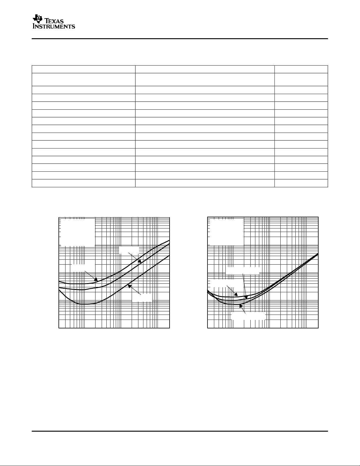
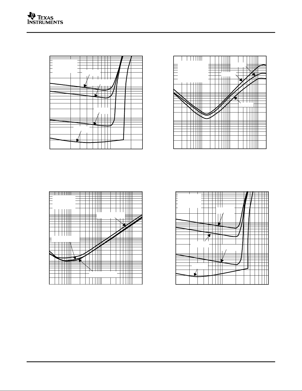
Table of Graphs
THD+N Total harmonic distortion plus noise vs Frequency
vs Output power 3, 6, 9, 12, 15, 18
PSSR Power supply rejection ratio vs Frequency 19, 20
V
I
CC
SNR Signal-to-noise ratio vs Voltage gain 35
Output noise voltage vs Frequency 21, 22
n
Crosstalk vs Frequency 23-26, 37, 38
Mute attenuation vs Frequency 27, 28
Open-loop gain vs Frequency 29, 30
Phase margin vs Frequency 29, 30
Phase vs Frequency 39-44
Output power vs Load resistance 31, 32
Supply current vs Supply voltage 33
Closed-loop gain vs Frequency 39-44
Power dissipation/amplifier vs Output power 45, 46
1, 2, 4, 5, 7, 8, 10, 11,
13, 14, 16, 17, 34, 36
TPA112
FIGURE
TOTAL HARMONIC DISTORTION + NOISE TOTAL HARMONIC DISTORTION + NOISE
vs vs
FREQUENCY FREQUENCY
Figure 1. Figure 2.
5
Page 6
www.ti.com
10 kHz
0.1
0.01
1
10
THD+N −Total Harmonic Distortion + Noise − %
PO − Output Power − mW
1 10 50
VDD = 3.3 V
RL = 32 Ω
AV = 1 V/V
CB = 1 µF
20 kHz
1 kHz
20 Hz
0.1
0.01
0.001
1
10
20 100 1k 10k 20k
VDD = 5 V
PO = 60 mW
RL = 32 Ω
CB = 1 µF
AV = 10 mW
THD+N −Total Harmonic Distortion + Noise − %
f − Frequency − Hz
AV = 5 mW
AV = 1 mW
0.1
0.01
0.001
1
10
20 100 1k 10k 20k
VDD = 5 V
RL = 32 Ω
AV = 1 V/V
CB = 1 µF
PO = 15 mW
THD+N −Total Harmonic Distortion + Noise − %
f − Frequency − Hz
PO = 30 mW
PO = 60 mW
THD+N −Total Harmonic Distortion + Noise − %
20 kHz
0.1
0.01
1
10
PO − Output Power − W
VDD = 5 V
AV = 1 V/V
RL = 32 Ω
CB = 1 µF
10 kHz
1 kHz
20 Hz
0.002 0.01 0.1 0.2
TPA112
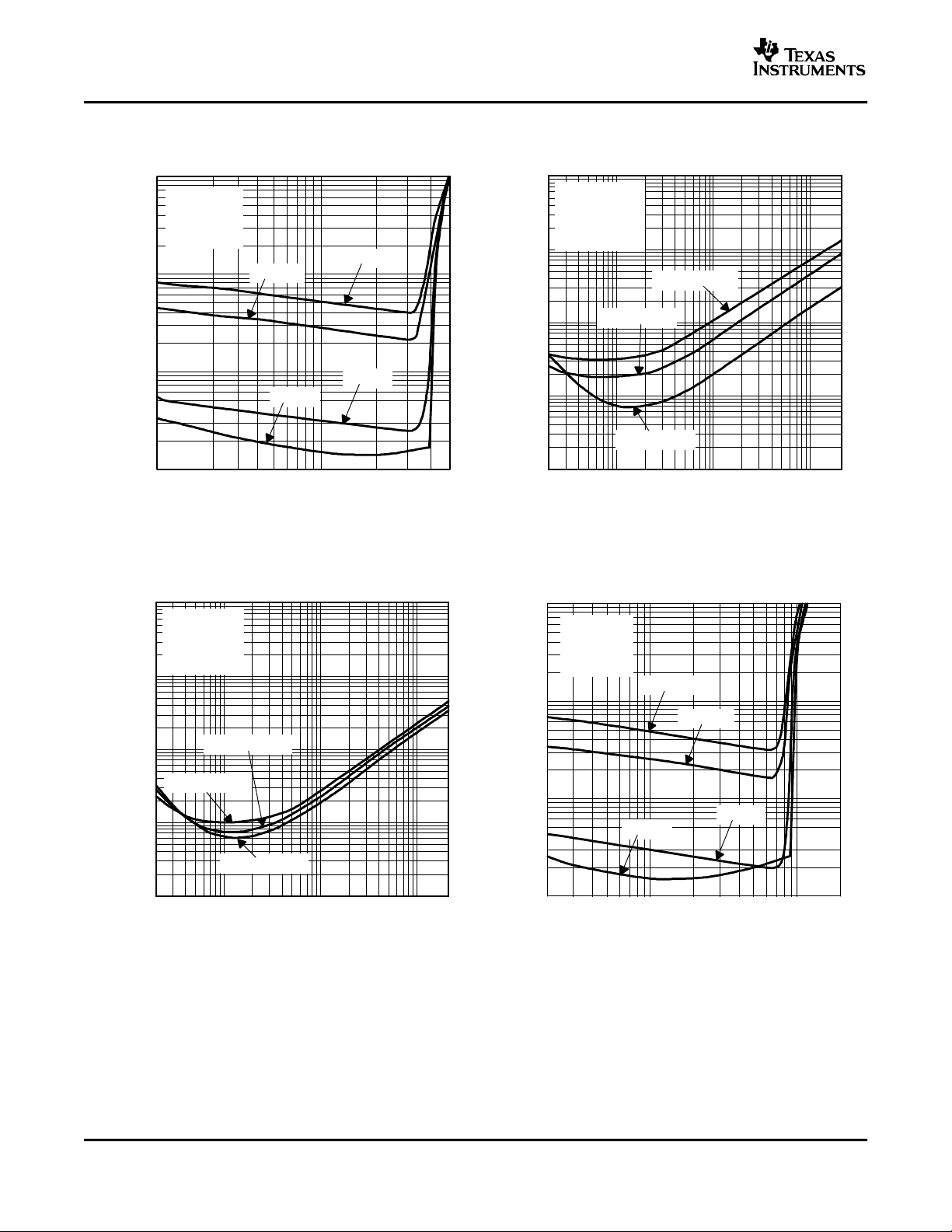
SLOS212E – AUGUST 1998 – REVISED JUNE 2004
TOTAL HARMONIC DISTORTION + NOISE TOTAL HARMONIC DISTORTION + NOISE
vs vs
OUTPUT POWER FREQUENCY
Figure 3. Figure 4.
TOTAL HARMONIC DISTORTION + NOISE TOTAL HARMONIC DISTORTION + NOISE
vs vs
FREQUENCY OUTPUT POWER
6
Figure 5. Figure 6.
Page 7
www.ti.com
0.1
0.01
0.001
1
10
20 100 1k 10k 20k
VDD = 3.3 V
RL = 10 kΩ
PO = 100 µF
CB = 1 µF
THD+N −Total Harmonic Distortion + Noise − %
f − Frequency − Hz
AV = 5 mW
AV = 2 mW
0.1
0.01
0.001
1
10
20 100 1k 10k 20k
VDD = 3.3 V
RL = 10 kΩ
AV = 1 V/V
CB = 1 µF
THD+N −Total Harmonic Distortion + Noise − %
f − Frequency − Hz
PO = 45 µW
PO = 130 µW
PO = 90 µW
5 10 100 200
THD+N −Total Harmonic Distortion + Noise − %
20 Hz
0.01
0.001
1
10
PO − Output Power − µW
10 kHz
1 kHz
20 Hz
0.1
VDD = 3.3 V
RL = 10 k Ω
AV = 1 V/V
CB = 1 µF
0.1
0.01
0.001
1
10
20 100 1k 10k 20k
VDD = 5 V
RL = 10 kΩ
PO = 300 µW
CB = 1 µF
THD+N −Total Harmonic Distortion + Noise − %
f − Frequency − Hz
AV = 1
AV = 2
AV = 5
TPA112
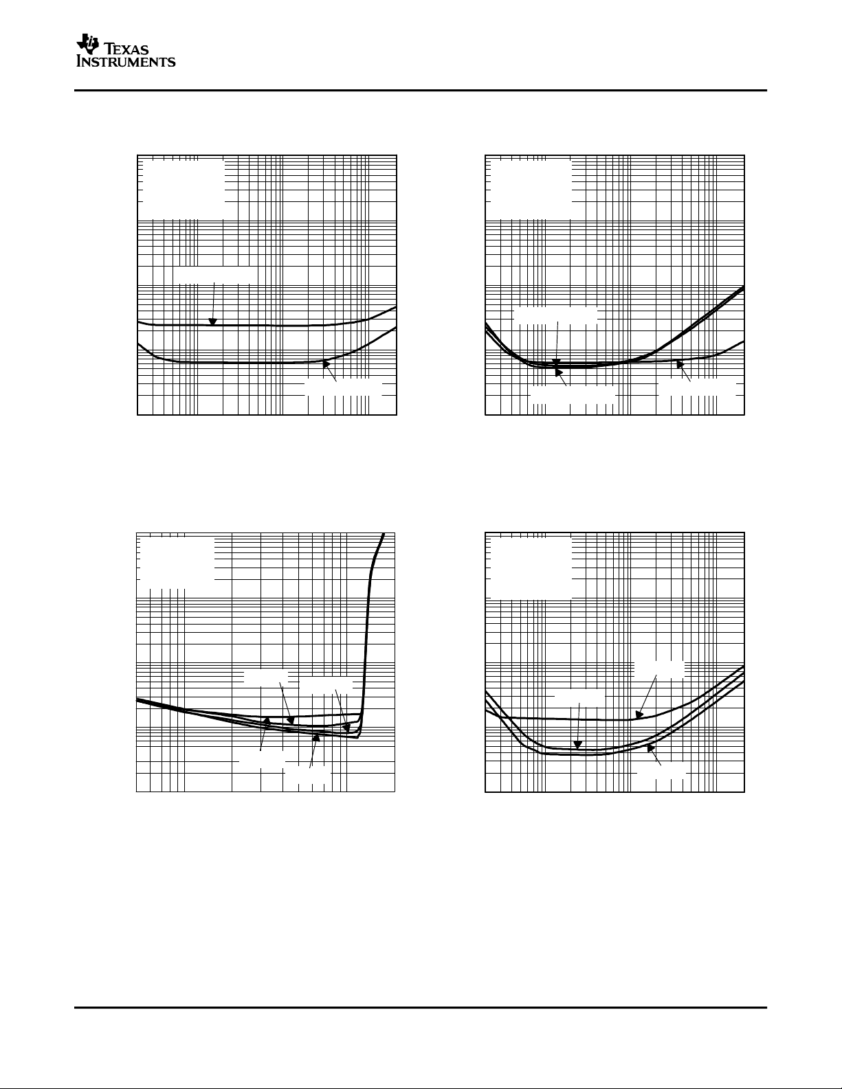
SLOS212E – AUGUST 1998 – REVISED JUNE 2004
TOTAL HARMONIC DISTORTION + NOISE TOTAL HARMONIC DISTORTION + NOISE
vs vs
FREQUENCY FREQUENCY
Figure 7. Figure 8.
TOTAL HARMONIC DISTORTION + NOISE TOTAL HARMONIC DISTORTION + NOISE
vs vs
OUTPUT POWER FREQUENCY
Figure 9. Figure 10.
7
Page 8
www.ti.com
0.1
0.01
0.001
1
10
20 100 1k 10k 20k
VDD = 5 V
RL = 10 kΩ
AV = 1 V/V
CB = 1 µF
THD+N −Total Harmonic Distortion + Noise − %
f − Frequency − Hz
PO = 300 µW
PO = 200 µW
PO = 100 µW
0.1
0.01
0.001
1
10
5 10 100 500
VDD = 5 V
RL = 10 kΩ
AV = 1 V/V
CB = 1 µ F
THD+N −Total Harmonic Distortion + Noise − %
20 Hz
1 kHz
20 kHz
10 kHz
PO − Output Power − µW
20
THD+N − Total Harmonic Distortion Plus Noise − %
f − Frequency − Hz
2
0.1
0.01
0.001
100 1k 10k 20k
1
AV = 1
AV = 2
AV = 5
V
DD
= 3.3 V
PO = 75 mW
RL = 8 Ω
CB = 1 µF
0.1
0.01
0.001
1
10
20 100 1k 10k 20k
VDD = 3.3 V
RL = 8 Ω
AV = 1 V/V
THD+N −Total Harmonic Distortion + Noise − %
f − Frequency − Hz
PO = 75 mW
PO = 15 mW
PO = 30 mW
TPA112
SLOS212E – AUGUST 1998 – REVISED JUNE 2004
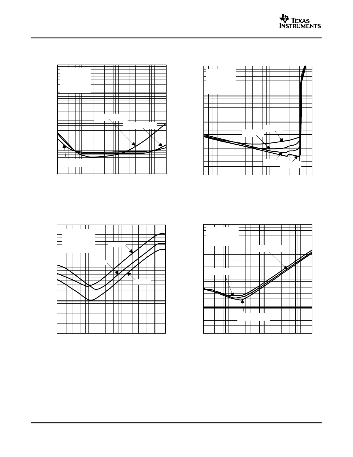
TOTAL HARMONIC DISTORTION + NOISE TOTAL HARMONIC DISTORTION + NOISE
vs vs
FREQUENCY OUTPUT POWER
Figure 11. Figure 12.
TOTAL HARMONIC DISTORTION + NOISE TOTAL HARMONIC DISTORTION + NOISE
vs vs
FREQUENCY FREQUENCY
8
Figure 13. Figure 14.
Page 9
www.ti.com
20
THD+N − Total Harmonic Distortion Plus Noise − %
f − Frequency − Hz
2
0.1
0.01
0.001
100 1k 10k 20k
1
AV = 1
AV = 2
AV = 5
V
DD
= 5 V
PO = 100 mW
RL = 8 Ω
CB = 1 µF
20 kHz
0.1
0.01
1
10
THD+N −Total Harmonic Distortion + Noise − %
PO − Output Power − W
10m 0.1 0.3
VDD = 3.3 V
RL = 8 Ω
AV = 1 V/V
10 kHz
1 kHz
20 Hz
0.1
0.01
0.001
1
10
20 100 1k 10k 20k
THD+N −Total Harmonic Distortion + Noise − %
f − Frequency − Hz
VDD = 5 V
RL = 8 kΩ
AV = 1 V/V
PO = 30 mW
PO = 60 mW
PO = 10 mW
20 kHz
0.1
0.01
1
10
THD+N −Total Harmonic Distortion + Noise − %
PO − Output Power − W
10m 0.1 1
1 kHz
20 Hz
10 kHz
VDD = 5 V
RL = 8 Ω
AV = 1 V/V
TPA112
SLOS212E – AUGUST 1998 – REVISED JUNE 2004
TOTAL HARMONIC DISTORTION + NOISE TOTAL HARMONIC DISTORTION + NOISE
vs vs
OUTPUT POWER FREQUENCY
Figure 15. Figure 16.
TOTAL HARMONIC DISTORTION + NOISE TOTAL HARMONIC DISTORTION + NOISE
vs vs
FREQUENCY OUTPUT POWER
Figure 17. Figure 18.
9
Page 10

www.ti.com
20 100 20k
f − Frequency − Hz
1k
−50
−70
−90
−60
−80
−100
VDD = 3.3 V
RL = 8 Ω to 10 kΩ
−40
−10
−30
0
−20
PSRR − Power Supply Rejection Ratio − dB
10k
CB = 0.1 µF
CB = 1 µF
CB = 2 µF
Bypass = 1.65 V
20 100 20k
f − Frequency − Hz
1k
−50
−70
−90
−60
−80
−100
VDD = 5 V
RL = 8 Ω to 10 kΩ
−40
−10
−30
0
−20
PSRR − Power Supply Rejection Ratio − dB
10k
CB = 0.1 µF
CB = 1 µF
CB = 2 µF
Bypass = 2.5 V
20
f − Frequency − Hz
20 100 1k 10k 20k
VDD = 3.3 V
BW = 10 Hz to 22 kHz
AV = 1 V/V
RL = 8 Ω to 10 kΩ
− Output Noise Voltage − VµV
n
10
1
1
10
20
f − Frequency − Hz
20 100 1k 10k 20k
V
DD
= 5 V
BW = 10 Hz to 22 kHz
RL = 8 Ω to 10 kΩ
AV = 1 V/V
− Output Noise Voltage − VµV
n
TPA112
SLOS212E – AUGUST 1998 – REVISED JUNE 2004
POWER SUPPLY REJECTION RATIO POWER SUPPLY REJECTION RATIO
vs vs
FREQUENCY FREQUENCY
Figure 19. Figure 20.
OUTPUT NOISE VOLTAGE OUTPUT NOISE VOLTAGE
vs vs
FREQUENCY FREQUENCY
10
Figure 21. Figure 22.
Page 11

www.ti.com
20 100 20k
f − Frequency − Hz
1k
−85
−95
−105
−90
−100
−110
PO = 25 mW
VDD = 3.3 V
RL = 32 Ω
CB = 1 µF
AV = 1 V/V
−80
−65
−75
−60
−70
Crosstalk − dB
10k
IN2 TO OUT1
IN1 TO OUT2
20 100 20k
f − Frequency − Hz
1k
−75
−85
−95
−80
−90
−100
PO = 100 mW
VDD = 3.3 V
RL = 8 Ω
CB = 1 µF
AV = 1 V/V
−70
−55
−65
−50
−60
Crosstalk − dB
10k
IN2 TO OUT1
IN1 TO OUT2
20 100 10k
f − Frequency − Hz
1k
−90
−100
−110
−95
−105
−85
−65
−80
−60
−75
−65
20k
V
DD
= 5 V
PO = 25 mW
CB = 1 µF
RL = 32 Ω
AV = 1 V/V
Crosstalk − dB
IN2 TO OUT1
IN1 TO OUT2
20 100 10k
f − Frequency − Hz
1k
−80
−90
−100
−85
−95
−75
−55
−70
−50
−65
−60
20k
V
DD
= 5 V
PO = 100 mW
CB = 1 µF
RL = 8 Ω
AV = 1 V/V
Crosstalk − dB
IN2 TO OUT1
IN1 TO OUT2
CROSSTALK CROSSTALK
vs vs
FREQUENCY FREQUENCY
TPA112
SLOS212E – AUGUST 1998 – REVISED JUNE 2004
Figure 23. Figure 24.
CROSSTALK CROSSTALK
vs vs
FREQUENCY FREQUENCY
Figure 25. Figure 26.
11
Page 12

www.ti.com
20 100 20k
f − Frequency − Hz
1k
−50
−70
−90
−60
−80
−100
VDD = 3.3 V
RL = 32 Ω
CB = 1 µF
−40
−10
−30
0
−20
Mute Attenuation − dB
10k
20 100 10k
f − Frequency − Hz
1k
−60
−80
−100
−70
−90
−50
−10
−40
0
−30
−20
20k
V
DD
= 5 V
CB = 1 µF
RL = 32 Ω
Mute Attenuation − dB
40
20
0
−20
60
80
−30°
0°
VDD = 3.3 V
TA = 25°C
No Load
100
30°
60°
90°
120°
150°
m
φ − Phase Margin
1k 100k
f − Frequency − Hz
10k 1M 10M100
Open-Loop Gain − dB
Phase
Gain
TPA112
SLOS212E – AUGUST 1998 – REVISED JUNE 2004
MUTE ATTENUATION MUTE ATTENUATION
vs vs
FREQUENCY FREQUENCY
Figure 27. Figure 28.
OPEN-LOOP GAIN AND PHASE MARGIN
vs
FREQUENCY
12
Figure 29.
Page 13

www.ti.com
f − Frequency − Hz
20
0
−20
40
80
100 1k 10k 10M1M100k
60
Open-Loop Gain − dB
100
VDD = 5 V
TA = 25°C
No Load
−30°
0°
30°
60°
90°
120°
150°
Phase
Gain
m
φ − Phase Margin
. .
RL − Load Resistance − Ω
100
40
0
16 32
80
60
20
24 40 64
120
8 48 56
THD+N = 1 %
VDD = 3.3 V
AV = 1 V/V
P
O
− Output Power − mW
250
100
0
16 32
200
150
50
24 40 64
300
8 48 56
THD+N = 1 %
VDD = 5 V
AV = 1 V/V
P
O
− Output Power − mW
RL − Load Resistance − Ω
OPEN-LOOP GAIN AND PHASE MARGIN
vs
FREQUENCY
TPA112
SLOS212E – AUGUST 1998 – REVISED JUNE 2004
Figure 30.
OUTPUT POWER OUTPUT POWER
vs vs
LOAD RESISTANCE LOAD RESISTANCE
Figure 31. Figure 32.
13
Page 14

www.ti.com
20
THD+N − Total Harmonic Distortion Plus Noise − %
f − Frequency − Hz
1
0.1
0.01
0.001
100 1k 10k 20k
V
I
= 1 V
AV = 1 V/V
RL = 10 kΩ
CB = 1 µF
VDD − Supply Voltage − V
1
0.6
0.2
3 4
0.8
0.4
0
3.5 4.5
1.4
2.5 5 5.5
1.2
I
DD
− Supply Current − mA
20
THD+N − Total Harmonic Distortion Plus Noise − %
f − Frequency − Hz
1
0.1
0.01
0.001
100 1k 10k 20k
V
DD
= 5 V
AV = 1 V/V
RL = 10 kΩ
CB = 1 µF
1
SNR − Signal−to−Ratio − dB
AV − Voltage Gain − V/V
104
100
96
92
5 7 9 10
94
98
102
862 43
V
I
= 1 V
TPA112
SLOS212E – AUGUST 1998 – REVISED JUNE 2004
SUPPLY CURRENT TOTAL HARMONIC DISTORTION + NOISE
vs vs
SUPPLY VOLTAGE FREQUENCY
Figure 33. Figure 34.
SIGNAL-TO-NOISE RATIO TOTAL HARMONIC DISTORTION + NOISE
vs vs
VOLTAGE GAIN FREQUENCY
14
Figure 35. Figure 36.
Page 15

www.ti.com
20
Crosstalk − dB
f − Frequency − Hz
−60
−100
−150
100 1k 10k 20k
−70
−80
−90
−110
−120
−130
−140
VDD = 3.3 V
VO = 1 V
RL = 10 kΩ
CB = 1 µF
IN2 to OUT1
IN1 to OUT2
20
Crosstalk − dB
f − Frequency − Hz
−60
−100
−150
100 1k 10k 20k
−70
−80
−90
−110
−120
−130
−140
VDD = 5 V
VO = 1 V
RL = 10 kΩ
CB = 1 µF
IN1 to OUT2
IN2 to OUT1
10
Closed−Loop Gain − dB
f − Frequency − Hz
−10
100 1k 10k 1M
30
20
10
0
100k
200°
180°
160°
140°
120°
100°
80°
Gain
Phase
Phase
VDD = 3.3 V
RI = 20 kΩ
RF = 20 kΩ
RL = 32 Ω
CI = 1 µF
AV = −1 V/V
CROSSTALK CROSSTALK
vs vs
FREQUENCY FREQUENCY
TPA112
SLOS212E – AUGUST 1998 – REVISED JUNE 2004
Figure 37. Figure 38.
CLOSED-LOOP GAIN AND PHASE
FREQUENCY
vs
Figure 39.
15
Page 16

www.ti.com
10
Closed−Loop Gain − dB
f − Frequency − Hz
−10
100 1k 10k 1M
30
20
10
0
100k
Phase
200°
180°
160°
140°
120°
100°
80°
Gain
Phase
VDD = 5 V
RI = 20 kΩ
RF = 20 kΩ
RL = 32 Ω
CI = 1 µF
AV = −1 V/V
10
Closed−Loop Gain − dB
f − Frequency − Hz
−20
100 1k 10k 1M
40
20
0
100k
Phase
200°
180°
160°
140°
120°
100°
80°
60°
Gain
Phase
VDD = 3.3 V
RI = 20 kΩ
RF = 20 kΩ
RL = 8 Ω
CI = 1 µF
AV = −1 V/V
TPA112
SLOS212E – AUGUST 1998 – REVISED JUNE 2004
CLOSED-LOOP GAIN AND PHASE
vs
FREQUENCY
16
CLOSED-LOOP GAIN AND PHASE
FREQUENCY
Figure 40.
vs
Figure 41.
Page 17

www.ti.com
10
Closed−Loop Gain − dB
f − Frequency − Hz
−10
100 1k 10k 1M
30
20
10
0
100k
Phase
200°
180°
160°
140°
120°
100°
80°
Gain
Phase
VDD = 3.3 V
RI = 20 kΩ
RF = 20 kΩ
RL = 10 kΩ
CI = 1 µF
AV = −1 V/V
10
Closed−Loop Gain − dB
f − Frequency − Hz
−20
100 1k 10k 1M
20
0
100k
Phase
200°
180°
160°
140°
120°
100°
80°
60°
40°
Gain
Phase
VDD = 5 V
RI = 20 kΩ
RF = 20 kΩ
RL = 8 Ω
CI = 1 µF
AV = −1 V/V
CLOSED-LOOP GAIN AND PHASE
vs
FREQUENCY
TPA112
SLOS212E – AUGUST 1998 – REVISED JUNE 2004
CLOSED-LOOP GAIN AND PHASE
FREQUENCY
Figure 42.
vs
Figure 43.
17
Page 18

www.ti.com
10
Closed−Loop Gain − dB
f − Frequency − Hz
−10
100 1k 10k 1M
30
20
10
0
100k
Phase
200°
180°
160°
140°
120°
100°
80°
Gain
Phase
VDD = 5 V
RI = 20 kΩ
RF = 20 kΩ
RL = 10 kΩ
CI = 1 µF
AV = −1 V/V
0
Amplifier Power − mW
Load Power − mW
80
40
20
0
80 120 180 200
10
30
50
14010020 6040
160
60
70
VDD = 3.3 V
8 Ω
16 Ω
64 Ω
32 Ω
0
Amplifier Power − mW
Load Power − mW
180
100
60
0
80 120 180 200
40
80
120
14010020 6040
160
140
160
VDD = 5 V
8 Ω
16 Ω
64 Ω
32 Ω
20
TPA112
SLOS212E – AUGUST 1998 – REVISED JUNE 2004
CLOSED-LOOP GAIN AND PHASE
vs
FREQUENCY
18
POWER DISSIPATION/AMPLIFIER POWER DISSIPATION/AMPLIFIER
vs vs
OUTPUT POWER OUTPUT POWER
Figure 45. Figure 46.
Figure 44.
Page 19

www.ti.com
Gain
R
F
R
I
Effective Impedance
RFR
I
RF R
I
f
co(lowpass)
1
2 R
FCF
f
co(highpass)
1
2 R
I
C
I
C
I
1
2 R
I
f
co(highpass)
TPA112
SLOS212E – AUGUST 1998 – REVISED JUNE 2004
APPLICATION INFORMATION
GAIN SETTING RESISTORS, R
The gain for the TPA112 is set by resistors R
and R
F
I
and RIaccording to Equation 1 .
F
Given that the TPA112 is an MOS amplifier, the input impedance is high. Consequently, input leakage currents
are not generally a concern, although noise in the circuit increases as the value of R
certain range of R
values is required for proper start-up operation of the amplifier. Taken together, it is
F
increases. In addition, a
F
recommended that the effective impedance seen by the inverting node of the amplifier be set between 5 kΩ and
20 kΩ. The effective impedance is calculated in Equation 2 .
As an example, consider an input resistance of 20 kΩ and a feedback resistor of 20 kΩ. The gain of the amplifier
would be -1 and the effective impedance at the inverting terminal would be 10 kΩ, which is within the
recommended range.
For high-performance applications, metal film resistors are recommended because they tend to have lower noise
levels than carbon resistors. For values of R
formed from R
and the inherent input capacitance of the MOS input structure. For this reason, a small
F
above 50 kΩ, the amplifier tends to become unstable due to a pole
F
compensation capacitor of approximately 5 pF should be placed in parallel with RF. In effect, this creates a
low-pass filter network with the cutoff frequency defined in Equation 3 .
For example, if R
is 100 kΩ and C
F
is 5 pF then f
F
co(lowpass)
is 318 kHz, which is well outside the audio range.
(1)
(2)
(3)
INPUT CAPACITOR, C
I
In the typical application, input capacitor CIis required to allow the amplifier to bias the input signal to the proper
dc level for optimum operation. In this case, C
and R
I
form a high-pass filter with the corner frequency
I
determined in Equation 4 .
The value of CIis important to consider, as it directly affects the bass (low-frequency) performance of the circuit.
Consider the example where R
is 20 kΩ and the specification calls for a flat bass response down to 20 Hz.
I
Equation 4 is reconfigured as Equation 5 .
In this example, C
is 0.4 µF, so one would likely choose a value in the range of 0.47 µF to 1 µF. A further
I
consideration for this capacitor is the leakage path from the input source through the input network (R
the feedback resistor (R
) to the load. This leakage current creates a dc offset voltage at the input to the amplifier
F
that reduces useful headroom, especially in high-gain applications (> 10). For this reason a low-leakage tantalum
or ceramic capacitor is the best choice. When polarized capacitors are used, the positive side of the capacitor
should face the amplifier input in most applications, as the dc level there is held at V
/2, which is likely higher
DD
that the source dc level. It is important to confirm the capacitor polarity in the application.
(4)
(5)
, CI) and
I
19
Page 20

www.ti.com
_
+
V
DD
R
R
Midrail
C
BYPASS
V
DD
R
R
Midrail
C
BYPASS
TLV2460
a) Midrail Voltage Generator Using a Simple
Resistor-Divider
b) Buffered Midrail Voltage Generator to Provide
Low Output Impedance
TPA112
SLOS212E – AUGUST 1998 – REVISED JUNE 2004
APPLICATION INFORMATION (continued)
POWER SUPPLY DECOUPLING, C
The TPA112 is a high-performance CMOS audio amplifier that requires adequate power supply decoupling to
ensure that the output total harmonic distortion (THD) is as low as possible. Power supply decoupling also
prevents oscillations for long lead lengths between the amplifier and the speaker. The optimum decoupling is
achieved by using two capacitors of different types that target different types of noise on the power supply leads.
For higher frequency transients, spikes, or digital hash on the line, a good low equivalent-series-resistance (ESR)
ceramic capacitor; typically, 0.1 µF, placed as close as possible to the device V
lower frequency noise signals, a larger aluminum electrolytic capacitor of 10 µF or greater placed near the power
amplifier is recommended.
MIDRAIL VOLTAGE
The TPA112 is a single-supply amplifier; so, it must be properly biased to accommodate audio signals. Normally,
the amplifier is biased at V
biasing the amplifier at a point other than V
applications where the circuitry driving the TPA112 has a different midrail voltage, it might make sense to use the
same midrail voltage for the TPA112, and possibly eliminate the use of the dc-blocking capacitors.
The two concerns with the midrail voltage source are the amount of noise present and its output impedance. Any
noise present on the midrail voltage source that is not present on the audio input signal will be input to the
amplifier, and passed to the output (and increased by the gain of the circuit). Common-mode noise is cancelled
out by the differential configuration of the circuit.
The output impedance of the circuit used to generate the midrail voltage needs to be low enough so as not to be
influenced by the audio signal path. A common method of generating the midrail voltage is to form a voltage
divider from the supply to ground, with a bypass capacitor from the common node to ground. This capacitor
improves the PSRR of the circuit. However, this circuit has a limited range of output impedances; so, to achieve
low output impedances, the voltage generated by the voltage divider is fed into a unity-gain amplifier to lower the
output impedance of the circuit.
/2, but it can actually be biased at any voltage between V
DD
S
lead, works best. For filtering
DD
and ground. However,
/2 reduces the amplifier's maximum output swing. In some
DD
DD
If a voltage step is applied to a speaker, it causes a noise pop. To reduce popping, the midrail voltage should
rise at a subsonic rate. That is, a rate less than the rise time of a 20-Hz waveform. If the voltage rises faster than
that, there is the possibility of a pop from the speaker.
Pop can also be heard in the speaker if the midrail voltage rises faster than the charge of either the input
coupling capacitor or the output coupling capacitor. If midrail rises first, the charging of the input and output
capacitors is heard in the speaker. To keep this noise as low as possible, the relationship shown in Equation 6
should be maintained.
20
Figure 47. Midrail Voltage Generator
Page 21

www.ti.com
1
C
B
R
SOURCE
1
CIR
I
1
RLC
C
1
C
B
R
SOURCE
1
CIR
I
6.25 50
f
(out high)
1
2 R
LCC
SLOS212E – AUGUST 1998 – REVISED JUNE 2004
APPLICATION INFORMATION (continued)
Where C
BYPASS
voltage divider (the parallel combination of the two resistors). For example, if the voltage divider is constructed
using two 20-kΩ resistors, then R
is the value of the bypass capacitor, and R
SOURCE
is 10 kΩ.
SOURCE
is the equivalent source impedance of the
TPA112
(6)
MIDRAIL BYPASS CAPACITOR, C
The midrail bypass capacitor C
B
B
serves several important functions. During start-up, C
determines the rate at
B
which the amplifier starts up. This helps to push the start-up pop noise into the subaudible range (so slow it can
not be heard). The second function is to reduce noise produced by the power supply caused by coupling into the
output drive signal. This noise is from the midrail generation circuit internal to the amplifier. The capacitor is fed
from the resistor divider with equivalent resistance of R
. To keep the start-up pop as low as possible, the
SOURCE
relationship shown in Equation 7 should be maintained.
As an example, consider a circuit where C
is 1 µF, R
B
SOURCE
= 160 kΩ, C
is 1 µF, and RIis 20 kΩ. Inserting
I
these values into the Equation 8 results in:
which satisfies the rule. Recommended values for bypass capacitor C
are 0.1 µF to 1 µF, ceramic or tantalum
B
low-ESR, for the best THD and noise performance.
OUTPUT COUPLING CAPACITOR, C
In the typical single-supply, single-ended (SE) configuration, an output coupling capacitor (C
C
) is required to
C
block the dc bias at the output of the amplifier, thus preventing dc currents in the load. As with the input coupling
capacitor, the output coupling capacitor and impedance of the load form a high-pass filter governed by
Equation 9 .
The main disadvantage, from a performance standpoint, is that the typically small load impedances drive the
low-frequency corner higher. Large values of C
example where a C
of 68 µF is chosen and loads vary from 32 Ω to 47 kΩ. Table 1 summarizes the frequency
C
are required to pass low frequencies into the load. Consider the
C
response characteristics of each configuration.
(7)
(8)
(9)
Table 1. Common Load Impedances vs Low Frequency
Output Characteristics in SE Mode
R
L
32 Ω 68 µF 73 Hz
10,000 Ω 68 µF 0.23 Hz
47,000 Ω 68 µF 0.05 Hz
C
C
LOWEST FREQUENCY
As Table 1 indicates, headphone response is adequate and drive into line level inputs (a home stereo for
example) is good.
The output coupling capacitor required in single-supply, SE mode also places additional constraints on the
selection of other components in the amplifier circuit. With the rules described earlier still valid, add the following
relationship:
• Output Pulldown Resistor, R
– Placing a 100-Ω resistor, R
+ R
C
O
, from the output side of the coupling capacitor to ground ensures the coupling
C
capacitor, CC, is charged before a plug is inserted into the jack. Without this resistor, the coupling capacitor
would charge rapidly upon insertion of a plug, leading to an audible pop in the headphones.
21
Page 22

www.ti.com
TPA112
SLOS212E – AUGUST 1998 – REVISED JUNE 2004
– Placing a 20-kΩ resistor, R
, from the output of the IC to ground ensures that the coupling capacitor fully
O
discharges at power down. If the supply is rapidly cycled without this capacitor, a small pop may be audible
in 10-kΩ loads.
• Using Low-ESR Capacitors
– Low-ESR capacitors are recommended throughout this application. A real capacitor can be modeled simply
as a resistor in series with an ideal capacitor. The voltage drop across this resistor minimizes the beneficial
effects of the capacitor in the circuit. The lower the equivalent value of this resistance, the more the real
capacitor behaves like an ideal capacitor.
5-V VERSUS 3.3-V OPERATION
The TPA112 is designed for operation over a supply range of 2.5 V to 5.5 V. This data sheet provides full
specifications for 5-V and 3.3-V operation because these are considered to be the two most common standard
voltages. There are no special considerations for 3.3-V versus 5-V operation as far as supply bypassing, gain
setting, or stability. The most important consideration is that of output power. Each amplifier in the TPA112 can
produce a maximum voltage swing of V
V
= 2.3 V, as opposed to V
O(PP)
O(PP)
maximum output power into the load before distortion begins to become significant.
– 1 V. This means, for 3.3-V operation, clipping starts to occur when
DD
= 4 V for 5-V operation. The reduced voltage swing subsequently reduces
22
Page 23

PACKAGE OPTION ADDENDUM
www.ti.com
7-May-2007
PACKAGING INFORMATION
Orderable Device Status
(1)
Package
Type
Package
Drawing
Pins Package
Qty
Eco Plan
TPA112D ACTIVE SOIC D 8 75 Green (RoHS &
no Sb/Br)
TPA112DG4 ACTIVE SOIC D 8 75 Green (RoHS &
no Sb/Br)
TPA112DGN ACTIVE MSOP-
Power
DGN 8 80 Green (RoHS &
no Sb/Br)
PAD
TPA112DGNG4 ACTIVE MSOP-
Power
DGN 8 80 Green (RoHS &
no Sb/Br)
PAD
TPA112DGNR ACTIVE MSOP-
Power
DGN 8 2500 Green (RoHS &
no Sb/Br)
PAD
TPA112DGNRG4 ACTIVE MSOP-
Power
DGN 8 2500 Green (RoHS &
no Sb/Br)
PAD
TPA112DR ACTIVE SOIC D 8 2500 Green (RoHS &
no Sb/Br)
TPA112DRG4 ACTIVE SOIC D 8 2500 Green (RoHS &
no Sb/Br)
TPA112EVM OBSOLETE 0 TBD Call TI Call TI
(1)
The marketing status values are defined as follows:
ACTIVE: Product device recommended for new designs.
LIFEBUY: TI has announced that the device will be discontinued, and a lifetime-buy period is in effect.
NRND: Not recommended for new designs. Device is in production to support existing customers, but TI does not recommend using this part in
a new design.
PREVIEW: Device has been announced but is not in production. Samples may or may not be available.
OBSOLETE: TI has discontinued the production of the device.
(2)
Lead/Ball Finish MSL Peak Temp
CU NIPDAU Level-1-260C-UNLIM
CU NIPDAU Level-1-260C-UNLIM
CU NIPDAU Level-1-260C-UNLIM
CU NIPDAU Level-1-260C-UNLIM
CU NIPDAU Level-1-260C-UNLIM
CU NIPDAU Level-1-260C-UNLIM
CU NIPDAU Level-1-260C-UNLIM
CU NIPDAU Level-1-260C-UNLIM
(3)
(2)
Eco Plan - The planned eco-friendly classification: Pb-Free (RoHS), Pb-Free (RoHS Exempt), or Green (RoHS & no Sb/Br) - please check
http://www.ti.com/productcontent for the latest availability information and additional product content details.
TBD: The Pb-Free/Green conversion plan has not been defined.
Pb-Free (RoHS): TI's terms "Lead-Free" or "Pb-Free" mean semiconductor products that are compatible with the current RoHS requirements
for all 6 substances, including the requirement that lead not exceed 0.1% by weight in homogeneous materials. Where designed to be soldered
at high temperatures, TI Pb-Free products are suitable for use in specified lead-free processes.
Pb-Free (RoHS Exempt): This component has a RoHS exemption for either 1) lead-based flip-chip solder bumps used between the die and
package, or 2) lead-based die adhesive used between the die and leadframe. The component is otherwise considered Pb-Free (RoHS
compatible) as defined above.
Green (RoHS & no Sb/Br): TI defines "Green" to mean Pb-Free (RoHS compatible), and free of Bromine (Br) and Antimony (Sb) based flame
retardants (Br or Sb do not exceed 0.1% by weight in homogeneous material)
(3)
MSL, Peak Temp. -- The Moisture Sensitivity Level rating according to the JEDEC industry standard classifications, and peak solder
temperature.
Important Information and Disclaimer:The information provided on this page represents TI's knowledge and belief as of the date that it is
provided. TI bases its knowledge and belief on information provided by third parties, and makes no representation or warranty as to the
accuracy of such information. Efforts are underway to better integrate information from third parties. TI has taken and continues to take
reasonable steps to provide representative and accurate information but may not have conducted destructive testing or chemical analysis on
incoming materials and chemicals. TI and TI suppliers consider certain information to be proprietary, and thus CAS numbers and other limited
information may not be available for release.
In no event shall TI's liability arising out of such information exceed the total purchase price of the TI part(s) at issue in this document sold by TI
to Customer on an annual basis.
Addendum-Page 1
Page 24

PACKAGE MATERIALS INFORMATION
www.ti.com
TAPE AND REEL INFORMATION
11-Mar-2008
*All dimensions are nominal
Device Package
TPA112DGNR MSOP-
Power
TPA112DR SOIC D 8 2500 330.0 12.4 6.4 5.2 2.1 8.0 12.0 Q1
Type
PAD
Package
Drawing
Pins SPQ Reel
Diameter
(mm)
DGN 8 2500 330.0 12.4 5.3 3.4 1.4 8.0 12.0 Q1
Reel
Width
W1 (mm)
A0 (mm) B0 (mm) K0 (mm) P1
(mm)W(mm)
Pin1
Quadrant
Pack Materials-Page 1
Page 25

PACKAGE MATERIALS INFORMATION
www.ti.com
11-Mar-2008
*All dimensions are nominal
Device Package Type Package Drawing Pins SPQ Length (mm) Width (mm) Height (mm)
TPA112DGNR MSOP-PowerPAD DGN 8 2500 358.0 335.0 35.0
TPA112DR SOIC D 8 2500 346.0 346.0 29.0
Pack Materials-Page 2
Page 26

Page 27

Page 28

Page 29

Page 30

IMPORTANT NOTICE
Texas Instruments Incorporated and its subsidiaries (TI) reserve the right to make corrections, modifications, enhancements, improvements,
and other changes to its products and services at any time and to discontinue any product or service without notice. Customers should
obtain the latest relevant information before placing orders and should verify that such information is current and complete. All products are
sold subject to TI’s terms and conditions of sale supplied at the time of order acknowledgment.
TI warrants performance of its hardware products to the specifications applicable at the time of sale in accordance with TI’s standard
warranty. Testing and other quality control techniques are used to the extent TI deems necessary to support this warranty. Except where
mandated by government requirements, testing of all parameters of each product is not necessarily performed.
TI assumes no liability for applications assistance or customer product design. Customers are responsible for their products and
applications using TI components. To minimize the risks associated with customer products and applications, customers should provide
adequate design and operating safeguards.
TI does not warrant or represent that any license, either express or implied, is granted under any TI patent right, copyright, mask work right,
or other TI intellectual property right relating to any combination, machine, or process in which TI products or services are used. Information
published by TI regarding third-party products or services does not constitute a license from TI to use such products or services or a
warranty or endorsement thereof. Use of such information may require a license from a third party under the patents or other intellectual
property of the third party, or a license from TI under the patents or other intellectual property of TI.
Reproduction of TI information in TI data books or data sheets is permissible only if reproduction is without alteration and is accompanied
by all associated warranties, conditions, limitations, and notices. Reproduction of this information with alteration is an unfair and deceptive
business practice. TI is not responsible or liable for such altered documentation. Information of third parties may be subject to additional
restrictions.
Resale of TI products or services with statements different from or beyond the parameters stated by TI for that product or service voids all
express and any implied warranties for the associated TI product or service and is an unfair and deceptive business practice. TI is not
responsible or liable for any such statements.
TI products are not authorized for use in safety-critical applications (such as life support) where a failure of the TI product would reasonably
be expected to cause severe personal injury or death, unless officers of the parties have executed an agreement specifically governing
such use. Buyers represent that they have all necessary expertise in the safety and regulatory ramifications of their applications, and
acknowledge and agree that they are solely responsible for all legal, regulatory and safety-related requirements concerning their products
and any use of TI products in such safety-critical applications, notwithstanding any applications-related information or support that may be
provided by TI. Further, Buyers must fully indemnify TI and its representatives against any damages arising out of the use of TI products in
such safety-critical applications.
TI products are neither designed nor intended for use in military/aerospace applications or environments unless the TI products are
specifically designated by TI as military-grade or "enhanced plastic." Only products designated by TI as military-grade meet military
specifications. Buyers acknowledge and agree that any such use of TI products which TI has not designated as military-grade is solely at
the Buyer's risk, and that they are solely responsible for compliance with all legal and regulatory requirements in connection with such use.
TI products are neither designed nor intended for use in automotive applications or environments unless the specific TI products are
designated by TI as compliant with ISO/TS 16949 requirements. Buyers acknowledge and agree that, if they use any non-designated
products in automotive applications, TI will not be responsible for any failure to meet such requirements.
Following are URLs where you can obtain information on other Texas Instruments products and application solutions:
Products Applications
Amplifiers amplifier.ti.com Audio www.ti.com/audio
Data Converters dataconverter.ti.com Automotive www.ti.com/automotive
DSP dsp.ti.com Broadband www.ti.com/broadband
Clocks and Timers www.ti.com/clocks Digital Control www.ti.com/digitalcontrol
Interface interface.ti.com Medical www.ti.com/medical
Logic logic.ti.com Military www.ti.com/military
Power Mgmt power.ti.com Optical Networking www.ti.com/opticalnetwork
Microcontrollers microcontroller.ti.com Security www.ti.com/security
RFID www.ti-rfid.com Telephony www.ti.com/telephony
RF/IF and ZigBee® Solutions www.ti.com/lprf Video & Imaging www.ti.com/video
Mailing Address: Texas Instruments, Post Office Box 655303, Dallas, Texas 75265
Copyright © 2008, Texas Instruments Incorporated
Wireless www.ti.com/wireless
 Loading...