


TPA0253
1-W MONO AUDIO POWER AMPLIFIER
WITH HEADPHONE DRIVE
SLOS280D – JANUARY 2000 – REVISED NOVEMBER 2002
DD
DGQ PACKAGE
(TOP VIEW)
1
2
3
4
5
10
9
8
7
6
LO/MO–
LIN
GND
ST/MN
RO/MO+
D Ideal for Notebook Computers, PDAs, and
Other Small Portable Audio Devices
D 1 W Into 8-Ω From 5-V Supply
D 0.3 W Into 8-Ω From 3-V Supply
D Stereo Head Phone Drive
D Mono (BTL) Signal Created by Summing
Left and Right Signals Internally
FILT_CAP
SHUTDOWN
V
BYPASS
RIN
D Wide Power Supply Compatibility
2.5 V to 5.5 V
D Low Supply Current
– 3.2 mA Typical at 5 V
– 2.7 mA Typical at 3 V
D Shutdown Control ...1 µA Typical
D Shutdown Pin Is TTL Compatible
D –40°C to 85°C Operating Temperature
Range
D Space-Saving, Thermally-Enhanced MSOP
Packaging
description
The TPA0253 is a 1-W mono bridge-tied-load (BTL) amplifier designed to drive speakers with as low as 8-Ω
impedance. The mono signal is created by summing left and right inputs internally. The amplifier can be
reconfigured on the fly to drive two stereo single-ended (SE) signals into headphones. This makes the device
ideal for use in small notebook computers, PDAs, digital personal audio players, anyplace a mono speaker and
stereo headphones are required. From a 5-V supply , the TPA0253 can deliver 1-W of power into an 8-Ω speaker .
The gain of the input stage is set by the user-selected input resistor and a 50-kΩ internal feedback resistor
(A
= – RF/RI). The power stage is internally configured with a gain of –1.25 V/V in SE mode, and –2.5 V/V in
V
BTL mode. Thus, the overall gain of the amplifier is 62.5 kΩ/R
in SE mode and 125 kΩ/RI in BTL mode. The
I
input terminals are high-impedance CMOS inputs, and can be used as summing nodes.
The TPA0253 is available in the 10-pin thermally-enhanced MSOP package (DGQ) and operates over an
ambient temperature range of –40°C to 85°C.
AVAILABLE OPTIONS
PACKAGED DEVICES
T
A
–40°C to 85°C TPA0253DGQ AEL
†
The DGQ package are available taped and reeled. To order a taped and reeled part, add the
suffix R to the part number (e.g., TPA0253DGQR).
Please be aware that an important notice concerning availability, standard warranty, and use in critical applications of
Texas Instruments semiconductor products and disclaimers thereto appears at the end of this data sheet.
MSOP
(DGQ)
†
MSOP
SYMBOLIZATION
PRODUCTION DATA information is current as of publication date.
Products conform to specifications per the terms of Texas Instruments
standard warranty. Production processing does not necessarily include
testing of all parameters.
POST OFFICE BOX 655303 • DALLAS, TEXAS 75265
Copyright 2002, Texas Instruments Incorporated
1

TPA0253
1-W MONO AUDIO POWER AMPLIFIER
WITH HEADPHONE DRIVE
SLOS280D – JANUARY 2000 – REVISED NOVEMBER 2002
schematic
V
DD
V
DD
3
4
BYPASS
C
BYP
GND
8
1 µF
Right
Audio
Input
Left
Audio
Input
From
System Control
C
i
C
i
1
FILT_CAP
5
RIN
R
i
R
i
9
LIN
2
SHUTDOWN
50 kΩ
M
U
X
BYPASS
50 kΩ
M
U
X
BYPASS
Shutdown
and Depop
Circuitry
50 kΩ
–
+
50 kΩ
50 kΩ
–
+
BYPASS
R
BYPASS
R
BYPASS
1.25*R
–
+
Stereo/Mono
Control
1.25*R
–
+
RO/MO+
ST/MN
LO/MO–
100 kΩ
C
6
7
10
V
DD
C
100 kΩ
C
C
1 kΩ
2
POST OFFICE BOX 655303 • DALLAS, TEXAS 75265
1-W MONO AUDIO POWER AMPLIFIER
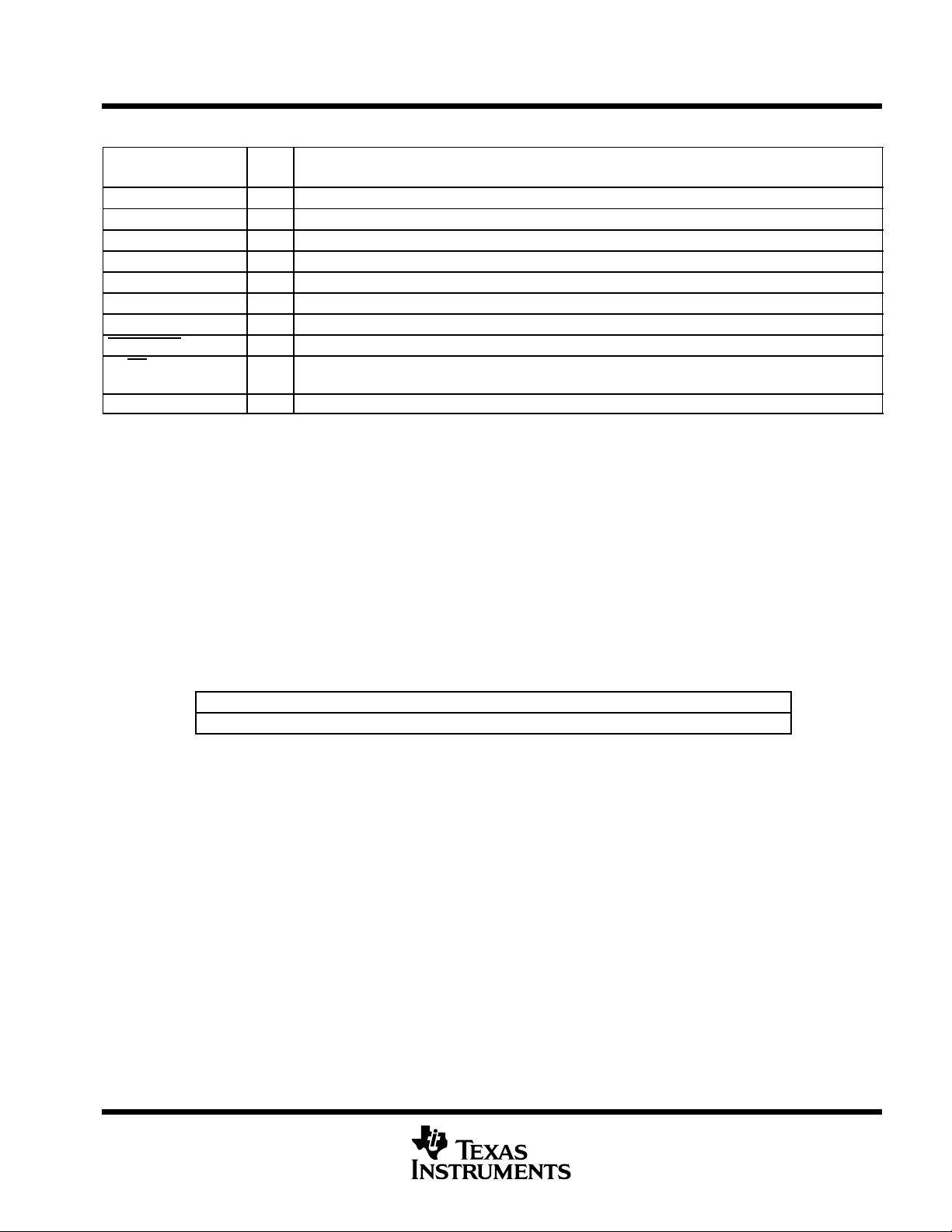
Terminal Functions
TPA0253
WITH HEADPHONE DRIVE
SLOS280D – JANUARY 2000 – REVISED NOVEMBER 2002
TERMINAL
NAME NO.
BYPASS 4 I Midrail bias voltage
FILT_CAP 1 Terminal used to filter power supply
GND 8 Ground terminal
LIN 9 I Left-channel input terminal
LO/MO– 10 O Left-output in SE mode and mono negative output in BTL mode.
RIN 5 I Right-channel input terminal
RO/MO+ 6 O Right-output in SE mode and mono positive output in BTL mode
SHUTDOWN 2 I TTL-compatible shutdown terminal
ST/MN 7 I Selects between stereo and mono mode. When held high, the amplifier is in SE stereo mode; while held
V
DD
I/O
low, the amplifier is in BTL mono mode.
3 I Positive power supply
DESCRIPTION
absolute maximum ratings over operating free-air temperature range (unless otherwise noted)
Supply voltage, V
Input voltage range, V
Continuous total power dissipation internally limited (see Dissipation Rating Table). . . . . . . . . . . . . . . . . . . . .
Operating free-air temperature range, T
Operating junction temperature range, T
Storage temperature range, T
Lead temperature 1,6 mm (1/16 inch) from case for 10 seconds 260°C. . . . . . . . . . . . . . . . . . . . . . . . . . . . . . .
‡
Stresses beyond those listed under “absolute maximum ratings” may cause permanent damage to the device. These are stress ratings only, and
functional operation of the device at these or any other conditions beyond those indicated under “recommended operating conditions” is not
implied. Exposure to absolute-maximum-rated conditions for extended periods may affect device reliability.
6 V. . . . . . . . . . . . . . . . . . . . . . . . . . . . . . . . . . . . . . . . . . . . . . . . . . . . . . . . . . . . . . . . . . . . . . . .
DD
–0.3 V to VDD +0.3 V. . . . . . . . . . . . . . . . . . . . . . . . . . . . . . . . . . . . . . . . . . . . . . . . . . . . . . .
I
(see Table 3) –40°C to 85°C. . . . . . . . . . . . . . . . . . . . . . . . . . . . . . . .
A
–40°C to 150°C. . . . . . . . . . . . . . . . . . . . . . . . . . . . . . . . . . . . . . . . . . .
–65°C to 150°C. . . . . . . . . . . . . . . . . . . . . . . . . . . . . . . . . . . . . . . . . . . . . . . . . . .
stg
J
†
PACKAGE
DGQ 2.14 W
‡
Please see the Texas Instruments document, PowerP AD Thermally Enhanced Package Application Report
(SLMA002), for more information on the PowerPAD package. The thermal data was measured on a PCB
layout based on the information in the section entitled T exas Instruments Recommended Board for PowerPAD
on page 33 of that document.
PowerPAD is a trademark of Texas Instruments.
TA ≤ 25°C DERATING FACTOR TA = 70°C TA = 85°C
DISSIPATION RATING TABLE
§
17.1 mW/°C 1.37 W 1.11 W
POST OFFICE BOX 655303 • DALLAS, TEXAS 75265
3

TPA0253
High level in ut voltage, V
IH
V
Low level in ut voltage, V
IL
V
Á
Á
Á
Á
Á
Á
Á
Á
Á
Á
Á
Á
Á
Á
Á
Á
Á
Á
Á
1-W MONO AUDIO POWER AMPLIFIER
WITH HEADPHONE DRIVE
SLOS280D – JANUARY 2000 – REVISED NOVEMBER 2002
recommended operating conditions
MIN MAX UNIT
Supply voltage, V
High-level input voltage, V
DD
IH
ST/MN
VDD = 3 V 2.7
VDD = 5 V 4.5
SHUTDOWN 2
VDD = 3 V 1.65
VDD = 5 V 2.75
Low-level input voltage, V
IL
ST/MN
SHUTDOWN 0.8
Operating free-air temperature, T
A
electrical characteristics at specified free-air temperature, VDD = 3 V , TA = 25°C (unless otherwise
noted)
PARAMETER TEST CONDITIONS
|VOO|
PSRR
Output offset voltage (measured differentially)
Power supply rejection ratio
|IIH| High-level input current
|IIL| Low-level input current
Z
I
I
DD
I
DD(SD)
R
F
ÁÁ
Input impedance
Supply current
Supply current, shutdown mode
Feedback resistor
ББББББББББ
RL = 4 Ω, ST/MN = 0 V, SHUTDOWN = 2 V
VDD = 2.9 V to 3.1 V, BTL mode
SHUTDOWN, VDD = 3.3 V, VI = V
ST/MN
, VDD = 3.3 V, VI = V
DD
DD
SHUTDOWN, VDD = 3.3 V, VI = 0 V
ST/MN
, VDD = 3.3 V, VI = 0 V
VDD = 2.5 V, SHUTDOWN = 2 V
SHUTDOWN = 0 V
VDD = 2.5 V, RL = 4 Ω, ST/MN = 1.375 V,
SHUTDOWN
ББББББББББ
= 2 V
MIN TYP MAX UNIT
Á
47
2.5
–40
65
50
2.7
50
Á
5.5
V
V
V
85
°C
30
mV
dB
1
µA
1
1
µA
1
kΩ
4
mA
1
10
µA
57
Á
kΩ
Á
operating characteristics, VDD = 3 V, T
= 25°C, R
A
= 8 Ω, f = 1 kHz (unless otherwise noted)
L
PARAMETER TEST CONDITIONS
P
O
ÁÁ
THD + N
ÁÁ
B
OM
V
n
Output power, see Note 1
ББББББББ
Total harmonic distortion plus
noise
ББББББББ
Maximum output power bandwidth
Supple ripple rejection ratio
Noise output voltage
p
THD = 0.1%,
THD = 0.1%
ÁÁÁ
Gain = 1.9 dB
PO = 250 mW,
ÁÁÁ
Gain = 1.9 dB,
f = 1 kHz,
C
= 0.47 µF,
(BYP)
BTL mode, Gain = 14 dB
SE mode, RL = 32 Ω
ББББББББ
f = 20 Hz to 20 kHz
БББББ
THD = 2%
C
= 0.47 µF
(BYP)
f = 20 Hz to 20 kHz
NOTE 1: Output power is measured at the output terminals of the device at f = 1 kHz.
MIN TYP MAX UNIT
ÁÁÁ
ÁÁÁÁÁÁ
BTL mode
SE mode
BTL mode
SE mode
300
30
0.2%
20
46
68
83
33
mW
ÁÁÁ
ÁÁÁ
kHz
dB
µV
RMS
4
POST OFFICE BOX 655303 • DALLAS, TEXAS 75265

TPA0253
ББББББББББББ
Á
Á
Á
Á
Á
Á
1-W MONO AUDIO POWER AMPLIFIER
WITH HEADPHONE DRIVE
SLOS280D – JANUARY 2000 – REVISED NOVEMBER 2002
electrical characteristics at specified free-air temperature, VDD = 5 V , TA = 25°C (unless otherwise
noted)
PARAMETER TEST CONDITIONS
|VOO|
PSRR
Output offset voltage (measured differentially)
Power supply rejection ratio
|IIH| High-level input current
|IIL| Low-level input current
Z
I
I
DD
I
DD(SD)
Input impedance
Supply current
Supply current, shutdown mode
RL = 4 Ω, ST/MN = 0 V, SHUTDOWN = 2 V
VDD = 4.9 V to 5.1 V, BTL mode
SHUTDOWN, VDD =5.5 V, VI = V
ST/MN
, VDD = 5.5 V, VI = V
DD
DD
SHUTDOWN, VDD = 5.5 V, VI = 0 V
ST/MN
, VDD = 5.5 V, VI = 0 V
SHUTDOWN = 2 V
SHUTDOWN = 0 V
MIN TYP MAX UNIT
30
mV
62
50
3.2
1
4.8
10
dB
1
µA
1
1
µA
1
kΩ
mA
µA
operating characteristics, VDD = 5 V, T
= 25°C, R
A
= 8 Ω, f = 1 kHz (unless otherwise noted)
L
PARAMETER TEST CONDITIONS
P
O
THD + N
B
OM
ÁÁ
V
n
Output power (see Note 1)
Total harmonic distortion plus
noise
Maximum output power
БББББББ
bandwidth
Supple ripple rejection ratio
Noise output voltage
THD = 0.1%,
THD = 0.1%,
PO = 1 W,
Gain = 8 dB,
ÁÁÁ
f = 1 kHz,
C
= 0.47 µF,
(BYP)
BTL mode
SE mode,
f = 20 Hz to 20 kHz
THD = 2%
БББББ
C
= 0.47 µF
(BYP)
f = 20 Hz to 20 kHz
NOTE 1: Output power is measured at the output terminals of the device at f = 1 kHz.
MIN TYP MAX UNIT
RL = 32 Ω
ÁÁÁÁÁÁ
BTL mode
SE mode
BTL mode
SE mode
85
0.33%
20
46
60
85
34
1
ÁÁÁ
µV
W
mW
kHz
dB
RMS
POST OFFICE BOX 655303 • DALLAS, TEXAS 75265
5

TPA0253
1-W MONO AUDIO POWER AMPLIFIER
WITH HEADPHONE DRIVE
SLOS280D – JANUARY 2000 – REVISED NOVEMBER 2002
MECHANICAL DATA
DGQ (S-PDSO-G10) PowerPAD PLASTIC SMALL-OUTLINE PACKAGE
0,50
10
1
1,07 MAX
3,05
2,95
0,27
0,17
6
3,05
2,95
5
Seating Plane
0,15
0,05
0,25
4,98
4,78
M
0,10
Thermal Pad
(See Note D)
0,15 NOM
Gage Plane
0°–ā6°
0,25
0,69
0,41
NOTES: A. All linear dimensions are in millimeters.
PowerPAD is a trademark of Texas Instruments.
6
B. This drawing is subject to change without notice.
C. Body dimensions do not include mold flash or protrusion.
D. The package thermal performance may be enhanced by bonding the thermal pad to an external thermal plane.
This pad is electrically and thermally connected to the backside of the die and possibly selected leads. The dimension of the thermal
pad is 1,40 mm (height as illustrated) × 1,80 (width as illustrated) mm (maximum). The pad is centered on the bottom of the package.
POST OFFICE BOX 655303 • DALLAS, TEXAS 75265
4073273/A 04/98

PACKAGE OPTION ADDENDUM
www.ti.com
18-Jul-2006
PACKAGING INFORMATION
Orderable Device Status
TPA0253DGQ ACTIVE MSOP-
(1)
Package
Type
Power
Package
Drawing
Pins Package
Qty
Eco Plan
DGQ 10 80 Green (RoHS &
no Sb/Br)
PAD
TPA0253DGQG4 ACTIVE MSOP-
Power
DGQ 10 80 Green (RoHS &
no Sb/Br)
PAD
TPA0253DGQR ACTIVE MSOP-
Power
DGQ 10 2500 Green (RoHS &
no Sb/Br)
PAD
TPA0253DGQRG4 ACTIVE MSOP-
Power
DGQ 10 2500 Green (RoHS &
no Sb/Br)
PAD
(1)
The marketing status values are defined as follows:
ACTIVE: Product device recommended for new designs.
LIFEBUY: TI has announced that the device will be discontinued, and a lifetime-buy period is in effect.
NRND: Not recommended for new designs. Device is in production to support existing customers, but TI does not recommend using this part in
a new design.
PREVIEW: Device has been announced but is not in production. Samples may or may not be available.
OBSOLETE: TI has discontinued the production of the device.
(2)
Eco Plan - The planned eco-friendly classification: Pb-Free (RoHS), Pb-Free (RoHS Exempt), or Green (RoHS & no Sb/Br) - please check
http://www.ti.com/productcontent for the latest availability information and additional product content details.
TBD: The Pb-Free/Green conversion plan has not been defined.
Pb-Free (RoHS): TI's terms "Lead-Free" or "Pb-Free" mean semiconductor products that are compatible with the current RoHS requirements
for all 6 substances, including the requirement that lead not exceed 0.1% by weight in homogeneous materials. Where designed to be soldered
at high temperatures, TI Pb-Free products are suitable for use in specified lead-free processes.
Pb-Free (RoHS Exempt): This component has a RoHS exemption for either 1) lead-based flip-chip solder bumps used between the die and
package, or 2) lead-based die adhesive used between the die and leadframe. The component is otherwise considered Pb-Free (RoHS
compatible) as defined above.
Green (RoHS & no Sb/Br): TI defines "Green" to mean Pb-Free (RoHS compatible), and free of Bromine (Br) and Antimony (Sb) based flame
retardants (Br or Sb do not exceed 0.1% by weight in homogeneous material)
(2)
Lead/Ball Finish MSL Peak Temp
CU NIPDAU Level-1-260C-UNLIM
CU NIPDAU Level-1-260C-UNLIM
CU NIPDAU Level-1-260C-UNLIM
CU NIPDAU Level-1-260C-UNLIM
(3)
(3)
MSL, Peak Temp. -- The Moisture Sensitivity Level rating according to the JEDEC industry standard classifications, and peak solder
temperature.
Important Information and Disclaimer:The information provided on this page represents TI's knowledge and belief as of the date that it is
provided. TI bases its knowledge and belief on information provided by third parties, and makes no representation or warranty as to the
accuracy of such information. Efforts are underway to better integrate information from third parties. TI has taken and continues to take
reasonable steps to provide representative and accurate information but may not have conducted destructive testing or chemical analysis on
incoming materials and chemicals. TI and TI suppliers consider certain information to be proprietary, and thus CAS numbers and other limited
information may not be available for release.
In no event shall TI's liability arising out of such information exceed the total purchase price of the TI part(s) at issue in this document sold by TI
to Customer on an annual basis.
Addendum-Page 1


IMPORTANT NOTICE
Texas Instruments Incorporated and its subsidiaries (TI) reserve the right to make corrections, modifications,
enhancements, improvements, and other changes to its products and services at any time and to
discontinue any product or service without notice. Customers should obtain the latest relevant information
before placing orders and should verify that such information is current and complete. All products are sold
subject to TI’s terms and conditions of sale supplied at the time of order acknowledgment.
TI warrants performance of its hardware products to the specifications applicable at the time of sale in
accordance with TI’s standard warranty. Testing and other quality control techniques are used to the extent
TI deems necessary to support this warranty. Except where mandated by government requirements, testing
of all parameters of each product is not necessarily performed.
TI assumes no liability for applications assistance or customer product design. Customers are responsible
for their products and applications using TI components. To minimize the risks associated with customer
products and applications, customers should provide adequate design and operating safeguards.
TI does not warrant or represent that any license, either express or implied, is granted under any TI patent
right, copyright, mask work right, or other TI intellectual property right relating to any combination, machine,
or process in which TI products or services are used. Information published by TI regarding third-party
products or services does not constitute a license from TI to use such products or services or a warranty or
endorsement thereof. Use of such information may require a license from a third party under the patents or
other intellectual property of the third party, or a license from TI under the patents or other intellectual
property of TI.
Reproduction of information in TI data books or data sheets is permissible only if reproduction is without
alteration and is accompanied by all associated warranties, conditions, limitations, and notices.
Reproduction of this information with alteration is an unfair and deceptive business practice. TI is not
responsible or liable for such altered documentation.
Resale of TI products or services with statements different from or beyond the parameters stated by TI for
that product or service voids all express and any implied warranties for the associated TI product or service
and is an unfair and deceptive business practice. TI is not responsible or liable for any such statements.
Following are URLs where you can obtain information on other Texas Instruments products and application
solutions:
Products
Applications
Amplifiers amplifier.ti.com Audio www.ti.com/audio
Data Converters dataconverter.ti.com Automotive www.ti.com/automotive
DSP dsp.ti.com Broadband www.ti.com/broadband
Interface interface.ti.com Digital Control www.ti.com/digitalcontrol
Logic logic.ti.com Military www.ti.com/military
Power Mgmt power.ti.com Optical Networking www.ti.com/opticalnetwork
Microcontrollers microcontroller.ti.com Security www.ti.com/security
Low Power Wireless www.ti.com/lpw Telephony www.ti.com/telephony
Video & Imaging www.ti.com/video
Wireless www.ti.com/wireless
Mailing Address: Texas Instruments
Post Office Box 655303 Dallas, Texas 75265
Copyright © 2007, Texas Instruments Incorporated

PACKAGE OPTION ADDENDUM
www.ti.com
18-Jul-2006
PACKAGING INFORMATION
Orderable Device Status
TPA0253DGQ ACTIVE MSOP-
(1)
Package
Type
Power
Package
Drawing
Pins Package
Qty
Eco Plan
DGQ 10 80 Green (RoHS &
no Sb/Br)
PAD
TPA0253DGQG4 ACTIVE MSOP-
Power
DGQ 10 80 Green (RoHS &
no Sb/Br)
PAD
TPA0253DGQR ACTIVE MSOP-
Power
DGQ 10 2500 Green (RoHS &
no Sb/Br)
PAD
TPA0253DGQRG4 ACTIVE MSOP-
Power
DGQ 10 2500 Green (RoHS &
no Sb/Br)
PAD
(1)
The marketing status values are defined as follows:
ACTIVE: Product device recommended for new designs.
LIFEBUY: TI has announced that the device will be discontinued, and a lifetime-buy period is in effect.
NRND: Not recommended for new designs. Device is in production to support existing customers, but TI does not recommend using this part in
a new design.
PREVIEW: Device has been announced but is not in production. Samples may or may not be available.
OBSOLETE: TI has discontinued the production of the device.
(2)
Eco Plan - The planned eco-friendly classification: Pb-Free (RoHS), Pb-Free (RoHS Exempt), or Green (RoHS & no Sb/Br) - please check
http://www.ti.com/productcontent for the latest availability information and additional product content details.
TBD: The Pb-Free/Green conversion plan has not been defined.
Pb-Free (RoHS): TI's terms "Lead-Free" or "Pb-Free" mean semiconductor products that are compatible with the current RoHS requirements
for all 6 substances, including the requirement that lead not exceed 0.1% by weight in homogeneous materials. Where designed to be soldered
at high temperatures, TI Pb-Free products are suitable for use in specified lead-free processes.
Pb-Free (RoHS Exempt): This component has a RoHS exemption for either 1) lead-based flip-chip solder bumps used between the die and
package, or 2) lead-based die adhesive used between the die and leadframe. The component is otherwise considered Pb-Free (RoHS
compatible) as defined above.
Green (RoHS & no Sb/Br): TI defines "Green" to mean Pb-Free (RoHS compatible), and free of Bromine (Br) and Antimony (Sb) based flame
retardants (Br or Sb do not exceed 0.1% by weight in homogeneous material)
(2)
Lead/Ball Finish MSL Peak Temp
CU NIPDAU Level-1-260C-UNLIM
CU NIPDAU Level-1-260C-UNLIM
CU NIPDAU Level-1-260C-UNLIM
CU NIPDAU Level-1-260C-UNLIM
(3)
(3)
MSL, Peak Temp. -- The Moisture Sensitivity Level rating according to the JEDEC industry standard classifications, and peak solder
temperature.
Important Information and Disclaimer:The information provided on this page represents TI's knowledge and belief as of the date that it is
provided. TI bases its knowledge and belief on information provided by third parties, and makes no representation or warranty as to the
accuracy of such information. Efforts are underway to better integrate information from third parties. TI has taken and continues to take
reasonable steps to provide representative and accurate information but may not have conducted destructive testing or chemical analysis on
incoming materials and chemicals. TI and TI suppliers consider certain information to be proprietary, and thus CAS numbers and other limited
information may not be available for release.
In no event shall TI's liability arising out of such information exceed the total purchase price of the TI part(s) at issue in this document sold by TI
to Customer on an annual basis.
Addendum-Page 1

PACKAGE MATERIALS INFORMATION
www.ti.com
TAPE AND REEL INFORMATION
11-Mar-2008
*All dimensions are nominal
Device Package
TPA0253DGQR MSOP-
Type
Power
PAD
Package
Drawing
DGQ 10 2500 330.0 12.4 5.3 3.4 1.4 8.0 12.0 Q1
Pins SPQ Reel
Diameter
(mm)
Reel
Width
W1 (mm)
A0 (mm) B0 (mm) K0 (mm) P1
(mm)W(mm)
Quadrant
Pin1
Pack Materials-Page 1

PACKAGE MATERIALS INFORMATION
www.ti.com
11-Mar-2008
*All dimensions are nominal
Device Package Type Package Drawing Pins SPQ Length (mm) Width (mm) Height (mm)
TPA0253DGQR MSOP-PowerPAD DGQ 10 2500 358.0 335.0 35.0
Pack Materials-Page 2


IMPORTANT NOTICE
Texas Instruments Incorporated and its subsidiaries (TI) reserve the right to make corrections, modifications, enhancements, improvements,
and other changes to its products and services at any time and to discontinue any product or service without notice. Customers should
obtain the latest relevant information before placing orders and should verify that such information is current and complete. All products are
sold subject to TI’s terms and conditions of sale supplied at the time of order acknowledgment.
TI warrants performance of its hardware products to the specifications applicable at the time of sale in accordance with TI’s standard
warranty. Testing and other quality control techniques are used to the extent TI deems necessary to support this warranty. Except where
mandated by government requirements, testing of all parameters of each product is not necessarily performed.
TI assumes no liability for applications assistance or customer product design. Customers are responsible for their products and
applications using TI components. To minimize the risks associated with customer products and applications, customers should provide
adequate design and operating safeguards.
TI does not warrant or represent that any license, either express or implied, is granted under any TI patent right, copyright, mask work right,
or other TI intellectual property right relating to any combination, machine, or process in which TI products or services are used. Information
published by TI regarding third-party products or services does not constitute a license from TI to use such products or services or a
warranty or endorsement thereof. Use of such information may require a license from a third party under the patents or other intellectual
property of the third party, or a license from TI under the patents or other intellectual property of TI.
Reproduction of TI information in TI data books or data sheets is permissible only if reproduction is without alteration and is accompanied
by all associated warranties, conditions, limitations, and notices. Reproduction of this information with alteration is an unfair and deceptive
business practice. TI is not responsible or liable for such altered documentation. Information of third parties may be subject to additional
restrictions.
Resale of TI products or services with statements different from or beyond the parameters stated by TI for that product or service voids all
express and any implied warranties for the associated TI product or service and is an unfair and deceptive business practice. TI is not
responsible or liable for any such statements.
TI products are not authorized for use in safety-critical applications (such as life support) where a failure of the TI product would reasonably
be expected to cause severe personal injury or death, unless officers of the parties have executed an agreement specifically governing
such use. Buyers represent that they have all necessary expertise in the safety and regulatory ramifications of their applications, and
acknowledge and agree that they are solely responsible for all legal, regulatory and safety-related requirements concerning their products
and any use of TI products in such safety-critical applications, notwithstanding any applications-related information or support that may be
provided by TI. Further, Buyers must fully indemnify TI and its representatives against any damages arising out of the use of TI products in
such safety-critical applications.
TI products are neither designed nor intended for use in military/aerospace applications or environments unless the TI products are
specifically designated by TI as military-grade or "enhanced plastic." Only products designated by TI as military-grade meet military
specifications. Buyers acknowledge and agree that any such use of TI products which TI has not designated as military-grade is solely at
the Buyer's risk, and that they are solely responsible for compliance with all legal and regulatory requirements in connection with such use.
TI products are neither designed nor intended for use in automotive applications or environments unless the specific TI products are
designated by TI as compliant with ISO/TS 16949 requirements. Buyers acknowledge and agree that, if they use any non-designated
products in automotive applications, TI will not be responsible for any failure to meet such requirements.
Following are URLs where you can obtain information on other Texas Instruments products and application solutions:
Products Applications
Amplifiers amplifier.ti.com Audio www.ti.com/audio
Data Converters dataconverter.ti.com Automotive www.ti.com/automotive
DSP dsp.ti.com Broadband www.ti.com/broadband
Clocks and Timers www.ti.com/clocks Digital Control www.ti.com/digitalcontrol
Interface interface.ti.com Medical www.ti.com/medical
Logic logic.ti.com Military www.ti.com/military
Power Mgmt power.ti.com Optical Networking www.ti.com/opticalnetwork
Microcontrollers microcontroller.ti.com Security www.ti.com/security
RFID www.ti-rfid.com Telephony www.ti.com/telephony
RF/IF and ZigBee® Solutions www.ti.com/lprf Video & Imaging www.ti.com/video
Mailing Address: Texas Instruments, Post Office Box 655303, Dallas, Texas 75265
Copyright © 2008, Texas Instruments Incorporated
Wireless www.ti.com/wireless
 Loading...