

TPA0132
2-W STEREO AUDIO POWER AMPLIFIER
WITH DC VOLUME CONTROL
SLOS223B – MAY 1999 – REVISED MARCH 2000
1
POST OFFICE BOX 655303 • DALLAS, TEXAS 75265
D
Compatible With PC 99 Desktop Line-Out
Into 10-kΩ Load
D
Compatible With PC 99 Portable Into 8-Ω
Load
D
Internal Gain Control, Which Eliminates
External Gain-Setting Resistors
D
DC Volume Control From +20 dB to –40 dB
D
2-W/Ch Output Power Into 3-Ω Load
D
PC-Beep Input
D
Depop Circuitry
D
Stereo Input MUX
D
Fully Differential Input
D
Low Supply Current and Shutdown Current
D
Surface-Mount Power Packaging
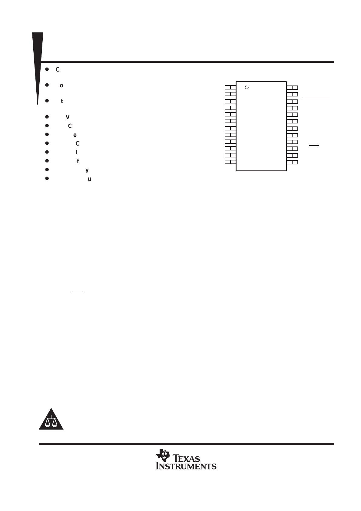
24-Pin TSSOP PowerP AD
description
The TPA0132 is a stereo audio power amplifier in a 24-pin TSSOP thermally enhanced package capable of
delivering 2 W of continuous RMS power per channel into 3-Ω loads. This device minimizes the number of
external components needed, which simplifies the design and frees up board space for other features. When
driving 1 W into 8-Ω speakers, the TP A0132 has less than 0.4% THD+N across its specified frequency range.
Included within this device is integrated depop circuitry that virtually eliminates transients that cause noise in
the speakers.
Amplifier gain is controlled by means of a dc voltage input on the VOLUME terminal. There are 31 discrete steps
covering the range of +20 dB (maximum volume setting) to –40 dB (minimum volume setting) in 2 dB steps.
When the VOLUME terminal exceeds 3.54 V, the device is muted. An internal input MUX allows two sets of
stereo inputs to the amplifier. In notebook applications, where internal speakers are driven as BTL and the line
outputs (often headphone drive) are required to be SE, the TP A0132 automatically switches into SE mode when
the SE/BTL
input is activated, and this effectively reduces the gain by 6 dB.
The TPA0132 consumes only 10 mA of supply current during normal operation. A miserly shutdown mode is
included that reduces the supply current to less than 150 µA.
The PowerPAD package (PWP) delivers a level of thermal performance that was previously achievable only
in TO-220-type packages. Thermal impedances of approximately 35°C/W are readily realized in multilayer PCB
applications. This allows the TP A0132 to operate at full power into 8-Ω loads at ambient temperatures of 85°C.
Please be aware that an important notice concerning availability, standard warranty, and use in critical applications of
Texas Instruments semiconductor products and disclaimers thereto appears at the end of this data sheet.
Copyright 2000, Texas Instruments Incorporated
PRODUCTION DATA information is current as of publication date.
Products conform to specifications per the terms of Texas Instruments
standard warranty. Production processing does not necessarily include
testing of all parameters.
1
2
3
4
5
6
7
8
9
10
11
12
24
23
22
21
20
19
18
17
16
15
14
13
PWP PACKAGE
(TOP VIEW)
GND
PCB ENABLE
VOLUME
LOUT+
LLINEIN
LHPIN
PV
DD
RIN
LOUT–
LIN
BYPASS
GND
GND
RLINEIN
SHUTDOWN
ROUT+
RHPIN
V
DD
PV
DD
CLK
ROUT–
SE/BTL
PC-BEEP
GND
PowerPAD is a trademark of Texas Instruments Incorporated.
TPA0132
2-W STEREO AUDIO POWER AMPLIFIER
WITH DC VOLUME CONTROL
SLOS223B – MAY 1999 – REVISED MARCH 2000
2
POST OFFICE BOX 655303 • DALLAS, TEXAS 75265
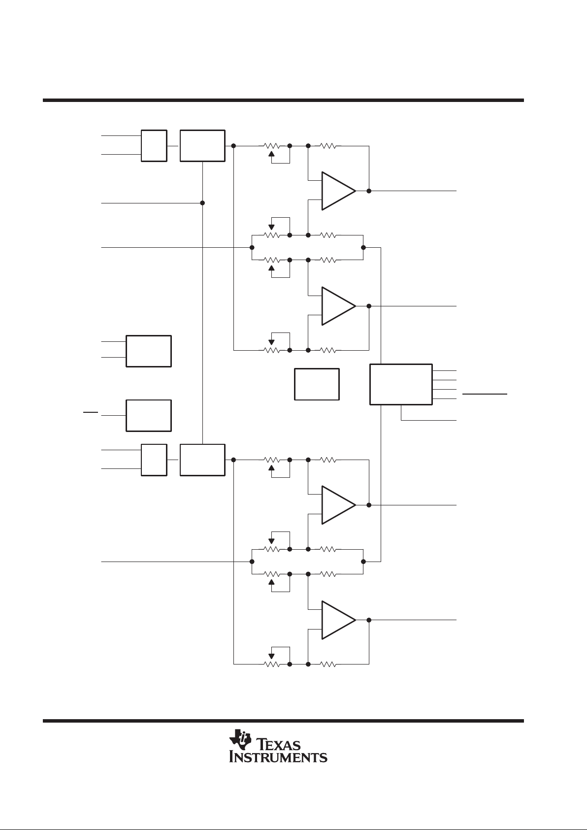
functional block diagram
ROUT+
–
+
–
+
R
MUX
32-Step
Volume
Control
PC
Beep
MUX
Control
Depop
Circuitry
Power
Management
–
+
–
+
L
MUX
32-Step
Volume
Control
RHPIN
RLINEIN
VOLUME
RIN
PC-BEEP
SE/BTL
LHPIN
LLINEIN
LIN
ROUT–
PV
DD
V
DD
BYPASS
SHUTDOWN
GND
LOUT+
LOUT–
PCB ENABLE
TPA0132
2-W STEREO AUDIO POWER AMPLIFIER
WITH DC VOLUME CONTROL
SLOS223B – MAY 1999 – REVISED MARCH 2000
3
POST OFFICE BOX 655303 • DALLAS, TEXAS 75265
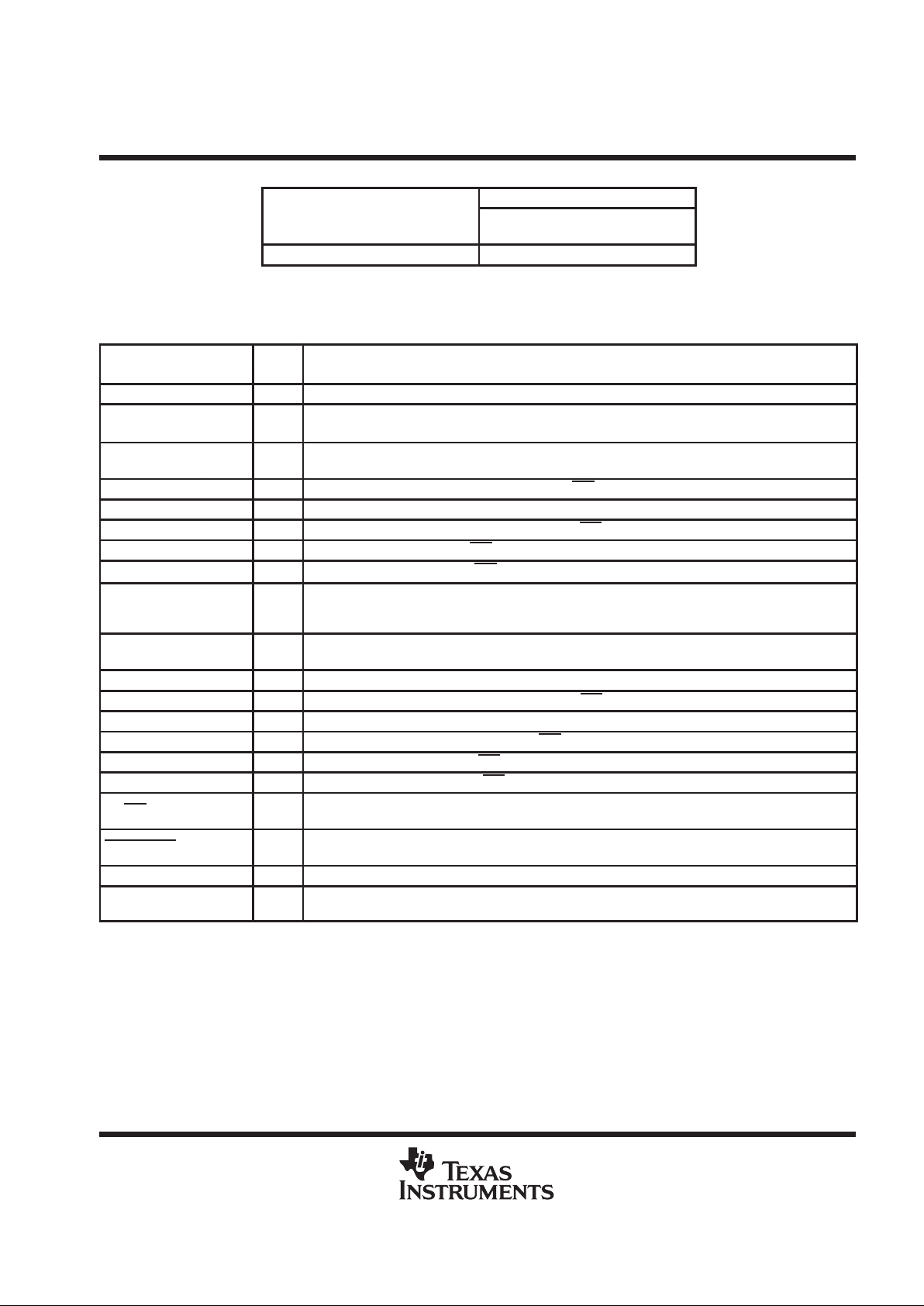
AVAILABLE OPTIONS
PACKAGED DEVICE
T
A
TSSOP
†
(PWP)
–40°C to 85°C TPA0132PWP
†
The PWP package is available taped and reeled. T o order a taped and reeled part,
add the suffix R to the part number (e.g., TPA0132PWPR).
Terminal Functions
TERMINAL
NAME NO.
I/O
DESCRIPTION
BYPASS 11 Tap to voltage divider for internal mid-supply bias generator
CLK 17 I
If a 47-nF capacitor is attached, the TPA0132 generates an internal clock. An external clock can override
the internal clock input to this terminal.
GND
1, 12
13, 24
Ground connection for circuitry. Connected to thermal pad.
LHPIN 6 I Left channel headphone input, selected when SE/BTL is held high
LIN 10 I Common left input for fully differential input. AC ground for single-ended inputs.
LLINEIN 5 I Left channel line negative input, selected when SE/BTL is held low
LOUT+ 4 O Left channel positive output in BTL mode and positive output in SE mode
LOUT– 9 O Left channel negative output in BTL mode and high-impedance in SE mode
PCB ENABLE 2 I
If this terminal is high, the detection circuitry for PC-BEEP is overridden and passes PC-BEEP through
the amplifier, regardless of its amplitude. If PCB ENABLE is floating or low, the amplifier continues to
operate normally .
PC-BEEP 14 I
The input for PC Beep mode. PC-BEEP is enabled when a > 1-V (peak-to-peak) square wave is input
to PC-BEEP or PCB ENABLE is high.
PV
DD
7, 18 I Power supply for output stage
RHPIN 20 I Right channel headphone input, selected when SE/BTL is held high
RIN 8 I Common right input for fully differential input. AC ground for single-ended inputs.
RLINEIN 23 I Right channel line input, selected when SE/BTL is held low
ROUT+ 21 O Right channel positive output in BTL mode and positive output in SE mode
ROUT– 16 O Right channel negative output in BTL mode and high-impedance in SE mode
SE/BTL 15 I
Input MUX control input. When this terminal is held high, the LHPIN or RHPIN and SE output is selected.
When this terminal is held low, the LLINEIN or RLINEIN and BTL output are selected.
SHUTDOWN 22 I
When held low, this terminal places the entire device, except PC-BEEP detect circuitry, in shutdown
mode.
V
DD
19 I Analog VDD input supply. This terminal needs to be isolated from PVDD to achieve highest performance.
VOLUME 3 I
VOLUME detects the dc level at the terminal and sets the gain for 31 discrete steps covering a range of
20 dB to –40 dB for dc levels of 0.15 V to 3.54. When the dc level is over 3.54 V, the device is muted.
TPA0132
2-W STEREO AUDIO POWER AMPLIFIER
WITH DC VOLUME CONTROL
SLOS223B – MAY 1999 – REVISED MARCH 2000
4
POST OFFICE BOX 655303 • DALLAS, TEXAS 75265
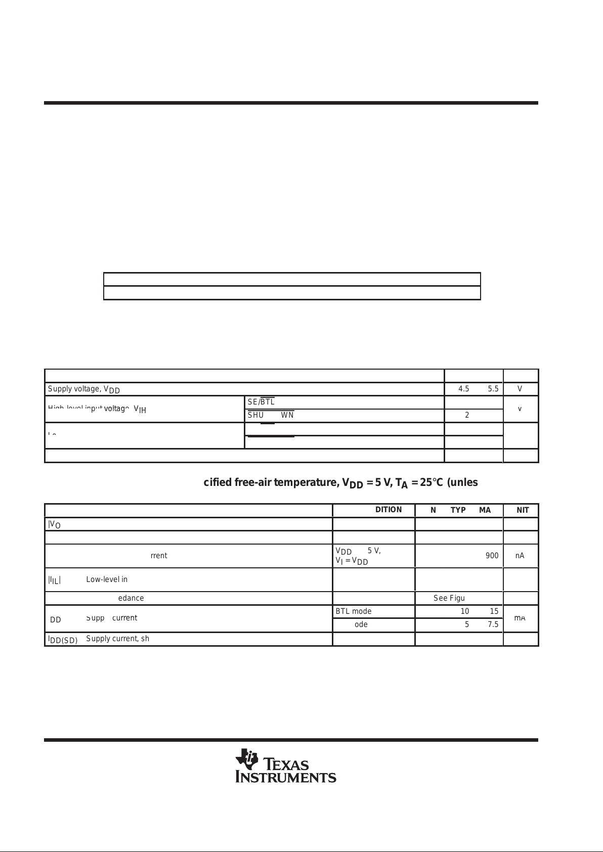
absolute maximum ratings over operating free-air temperature range (unless otherwise noted)
‡
Supply voltage, VDD 6 V. . . . . . . . . . . . . . . . . . . . . . . . . . . . . . . . . . . . . . . . . . . . . . . . . . . . . . . . . . . . . . . . . . . . . . . .
Input voltage, VI –0.3 V to VDD +0.3 V. . . . . . . . . . . . . . . . . . . . . . . . . . . . . . . . . . . . . . . . . . . . . . . . . . . . . . . . . . . .
Continuous total power dissipation internally limited (see Dissipation Rating Table). . . . . . . . . . . . . . . . . . . . .
Operating free-air temperature range, T
A
–40°C to 85°C. . . . . . . . . . . . . . . . . . . . . . . . . . . . . . . . . . . . . . . . . . . .
Operating junction temperature range, TJ –40°C to 150°C. . . . . . . . . . . . . . . . . . . . . . . . . . . . . . . . . . . . . . . . . . .
Storage temperature range, T
stg
–65°C to 150°C. . . . . . . . . . . . . . . . . . . . . . . . . . . . . . . . . . . . . . . . . . . . . . . . . . .
Lead temperature 1,6 mm (1/16 inch) from case for 10 seconds 260°C. . . . . . . . . . . . . . . . . . . . . . . . . . . . . . .
‡
Stresses beyond those listed under “absolute maximum ratings” may cause permanent damage to the device. These are stress ratings only, and
functional operation of the device at these or any other conditions beyond those indicated under “recommended operating conditions” is not
implied. Exposure to absolute-maximum-rated conditions for extended periods may affect device reliability.
DISSIPATION RATING TABLE
PACKAGE
TA ≤ 25°C DERATING FACTOR TA = 70°C TA = 85°C
PWP 2.7 W
§
21.8 mW/°C 1.7 W 1.4 W
§
Please see the Texas Instruments document,
PowerPAD Thermally Enhanced Package Application Report
(literature number SLMA002), for more information on the PowerPAD package. The thermal data was
measured on a PCB layout based on the information in the section entitled
T exas Instruments Recommended
Board for PowerPAD
on page 33 of the before mentioned document.
recommended operating conditions
MIN MAX UNIT
Supply voltage, V
DD
4.5
5.5
V
p
SE/BTL 4
High-level input voltage, V
IH
SHUTDOWN 2
V
p
SE/BTL 3
Low-level input voltage, V
IL
SHUTDOWN 0.8
V
Operating free-air temperature, T
A
–40
85
°C
electrical characteristics at specified free-air temperature, VDD = 5 V , TA = 25°C (unless otherwise
noted)
PARAMETER TEST CONDITIONS
MIN TYP MAX UNIT
|VOO|
Output offset voltage (measured differentially)
VI = 0, AV = 2
25
mV
PSRR
Power supply rejection ratio
VDD = 4 V to 5 V
67
dB
|IIH| High-level input current
VDD = 5.5 V,
VI = V
DD
ÁÁÁÁÁ
Á
900
Á
Á
nA
|IIL| Low-level input current
VDD = 5.5 V,
VI = 0 V
900
nA
Z
I
Input impedance
See Figure 28
pp
BTL mode
10
15
IDDSupply current
SE mode
5
7.5
mA
I
DD(SD)
Supply current, shutdown mode
150
300
µA
TPA0132
2-W STEREO AUDIO POWER AMPLIFIER
WITH DC VOLUME CONTROL
SLOS223B – MAY 1999 – REVISED MARCH 2000
5
POST OFFICE BOX 655303 • DALLAS, TEXAS 75265
operating characteristics, VDD = 5 V , T
A
= 25°C, R
L
= 4 Ω, Gain = 2 V/V , BTL mode (unless otherwise
noted)
PARAMETER TEST CONDITIONS
MIN TYP MAX UNIT
P
O
БББББББББББ
Output power
THD = 1%,
f = 1 kHz
2
W
THD + N
БББББББББББ
Total harmonic distortion plus noise
PO = 1 W,
f = 20 Hz to 15 kHz
0.4%
B
OM
БББББББББББ
Maximum output power bandwidth
THD = 5%
>15
kHz
БББББББББББ
pp
pp
f = 1 kHz,
BTL mode
65
БББББББББББ
Supply ripple rejection ratio
,
CB = 0.47 µF
SE mode
60
dB
p
CB = 0.47 µF,
BTL mode
34
V
n
БББББББББББ
Noise output voltage
B
µ
f = 20 Hz to 20 kHz
SE mode
44
µ
V
RMS
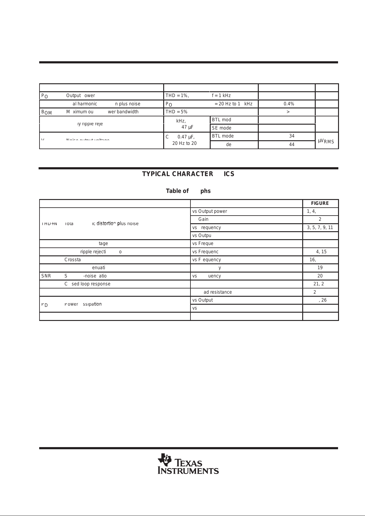
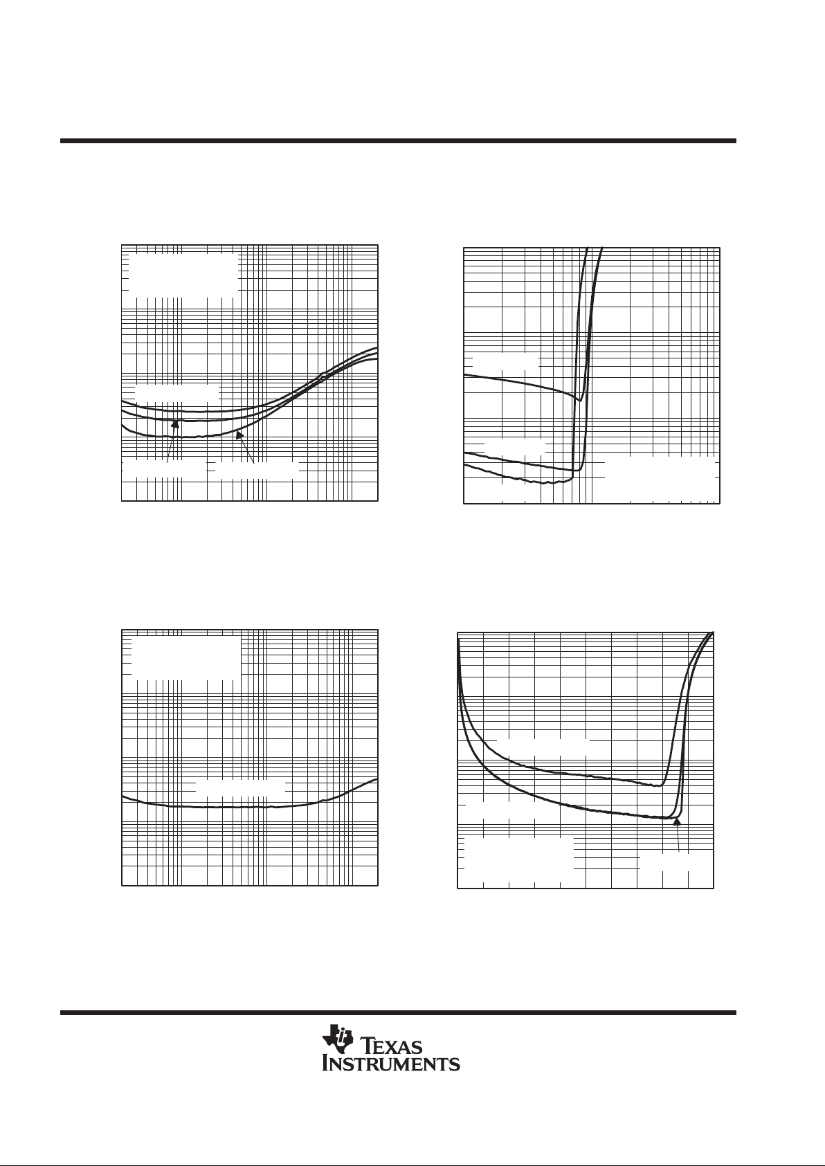
TYPICAL CHARACTERISTICS
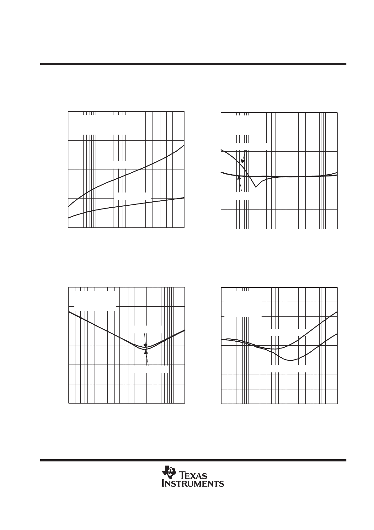
Table of Graphs
FIGURE
vs Output power 1, 4, 6, 8, 10
p
vs Gain 2
THD+N
Total harmonic distortion plus noise
vs Frequency 3, 5, 7, 9, 11
vs Output voltage 12
V
n
Output noise voltage vs Frequency 13
Supply ripple rejection ratio vs Frequency 14, 15
Crosstalk vs Frequency 16, 17, 18
Shutdown attenuation vs Frequency 19
SNR Signal-to-noise ratio vs Frequency 20
Closed loop response 21, 22
P
O
Output power vs Load resistance 23, 24
p
vs Output power 25, 26
PDPower dissipation
vs Ambient temperature 27
Z
I
Input impedance vs Gain 28
TPA0132
2-W STEREO AUDIO POWER AMPLIFIER
WITH DC VOLUME CONTROL
SLOS223B – MAY 1999 – REVISED MARCH 2000
6
POST OFFICE BOX 655303 • DALLAS, TEXAS 75265
TYPICAL CHARACTERISTICS
Figure 1
0.1%
0.01%
0.5 0.75 1 1.25 1.5 1.75 2
1%
10%
2.25 2.5 2.75 3
PO – Output Power – W
AV = +20 to 0 dB
f = 1 kHz
BTL
THD+N –Total Harmonic Distortion + Noise
TOTAL HARMONIC DISTORTION PLUS NOISE
vs
OUTPUT POWER
RL = 8 Ω
RL = 3 Ω
RL = 4 Ω
Figure 2
0.01%
–40 –30 –20 –10 0
THD+N –Total Harmonic Distortion + Noise
A - Voltage Gain - dB
TOTAL HARMONIC DISTORTION PLUS NOISE
vs
GAIN
1%
0.1%
10 20
V
PO = 1 W for AV≥6dB
VO = 1 V
RMS
for AV≤4 dB
RL = 8 Ω
BTL
Figure 3
0.01%
10%
20 100 1k 10k 20k
THD+N –Total Harmonic Distortion + Noise
f – Frequency – Hz
TOTAL HARMONIC DISTORTION PLUS NOISE
vs
FREQUENCY
1%
0.1%
RL = 3 Ω
AV = +20 to 0 dB
BTL
PO = 1.75 W
PO = 0.5 W
PO = 1 W
Figure 4
0.1%
0.01%
0.01 0.1
1%
10%
110
f = 20 Hz
f = 1 kHz
PO – Output Power – W
RL = 3 Ω
AV = +20 to 0 dB
BTL
THD+N –Total Harmonic Distortion + Noise
TOTAL HARMONIC DISTORTION PLUS NOISE
vs
OUTPUT POWER
f = 20 kHz
TPA0132
2-W STEREO AUDIO POWER AMPLIFIER
WITH DC VOLUME CONTROL
SLOS223B – MAY 1999 – REVISED MARCH 2000
7
POST OFFICE BOX 655303 • DALLAS, TEXAS 75265
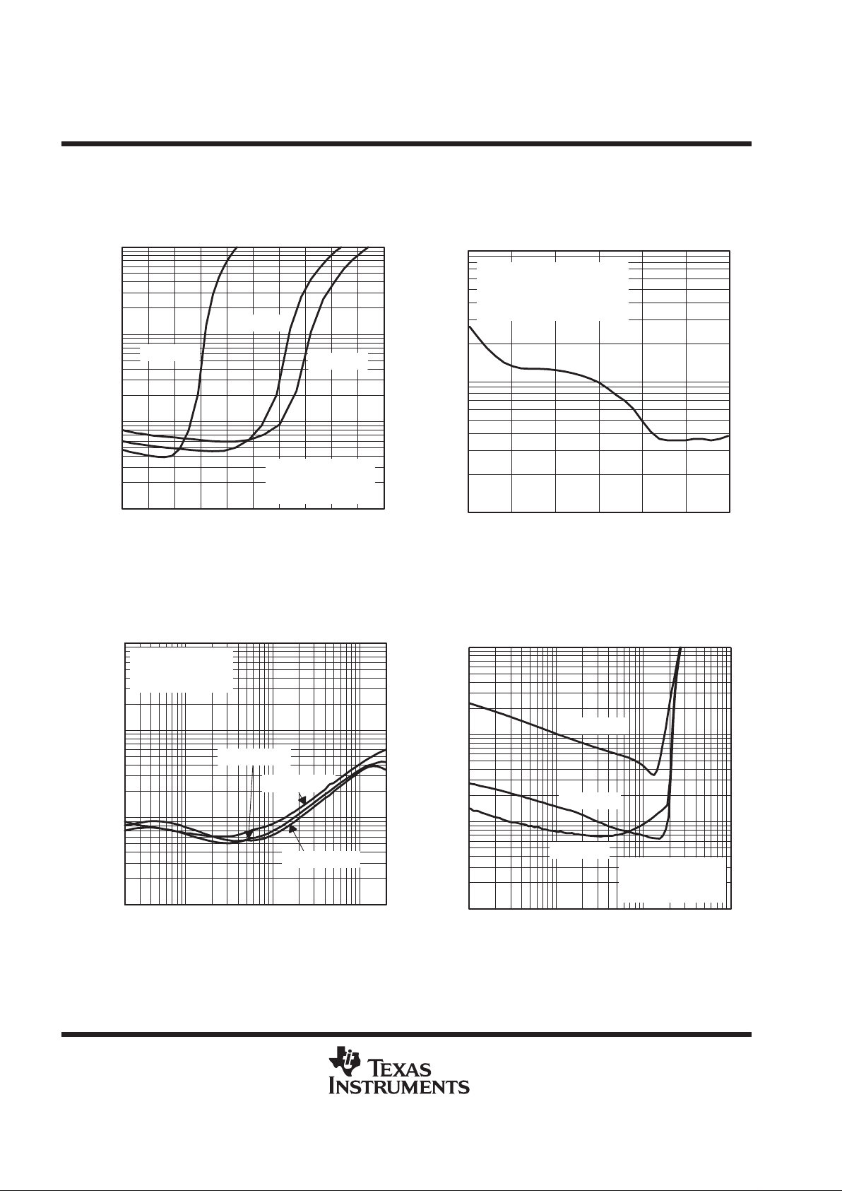
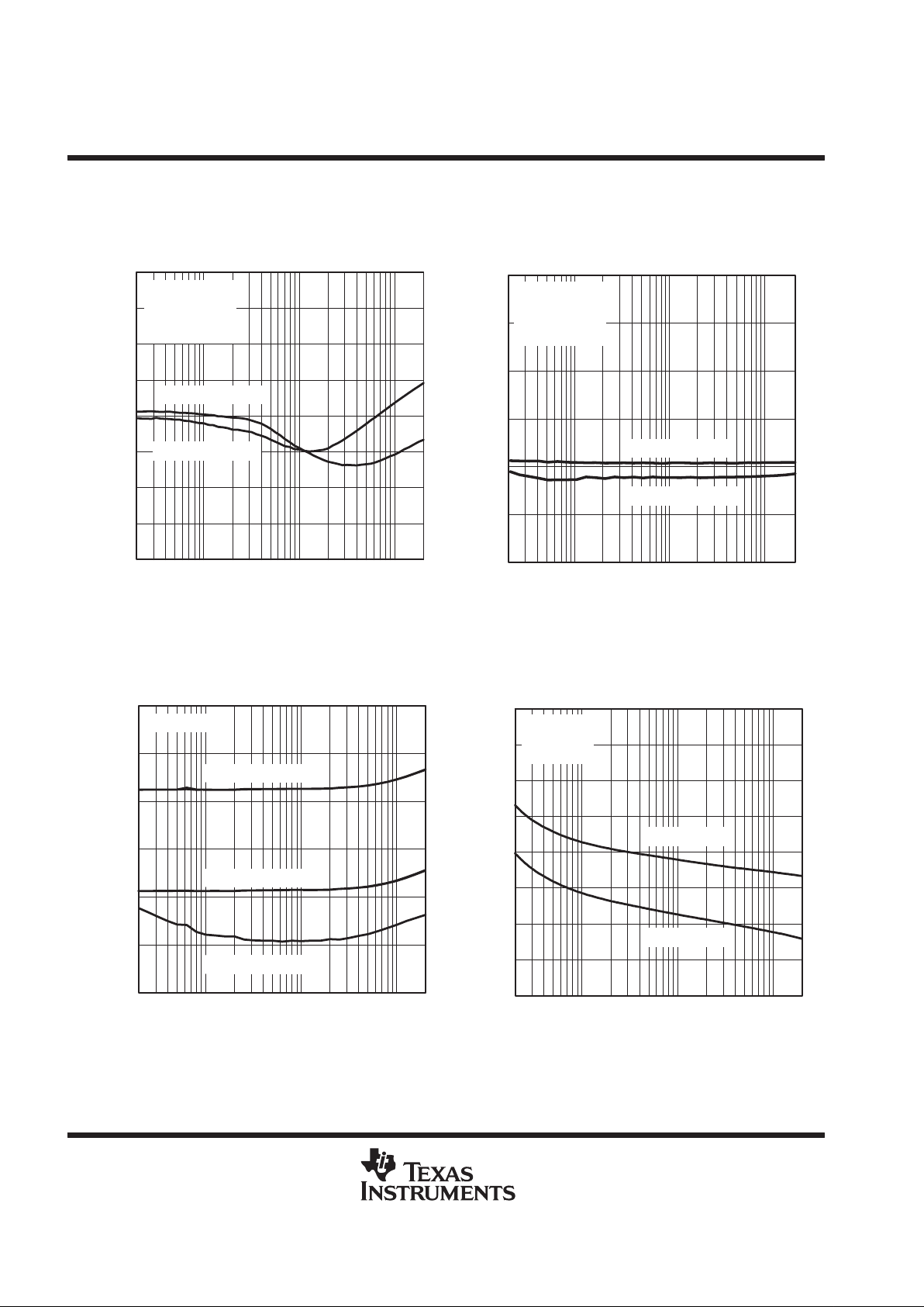
TYPICAL CHARACTERISTICS
Figure 5
0.1%
0.01%
20 100
1%
10%
1k 10k
f – Frequency – Hz
RL = 4 Ω
AV = +20 to 0 dB
BTL
THD+N –Total Harmonic Distortion + Noise
TOTAL HARMONIC DISTORTION PLUS NOISE
vs
FREQUENCY
PO= 0.25 W
20k
PO= 1 W
PO=1.5 W
Figure 6
0.1%
0.01%
0.01 0.1
1%
10%
110
f = 20 Hz
f = 1 kHz
PO – Output Power – W
THD+N –Total Harmonic Distortion + Noise
TOTAL HARMONIC DISTORTION PLUS NOISE
vs
OUTPUT POWER
f = 20 kHz
RL = 4 Ω
AV = +20 to 0 dB
BTL
Figure 7
0.01%
10%
20 100 1k 10k 20k
THD+N –Total Harmonic Distortion + Noise
f – Frequency – Hz
TOTAL HARMONIC DISTORTION PLUS NOISE
vs
FREQUENCY
1%
0.1%
PO = 0.25 W
PO = 0.5 W
PO = 1 W
RL = 8 Ω
AV = +20 to 0 dB
BTL
Figure 8
0.1%
0.01%
0.01 0.1
1%
10%
110
f = 20 Hz
f = 1 kHz
PO – Output Power – W
THD+N –Total Harmonic Distortion + Noise
TOTAL HARMONIC DISTORTION PLUS NOISE
vs
OUTPUT POWER
f = 20 kHz
RL = 8 Ω
AV = +20 to 0 dB
BTL
TPA0132
2-W STEREO AUDIO POWER AMPLIFIER
WITH DC VOLUME CONTROL
SLOS223B – MAY 1999 – REVISED MARCH 2000
8
POST OFFICE BOX 655303 • DALLAS, TEXAS 75265
TYPICAL CHARACTERISTICS
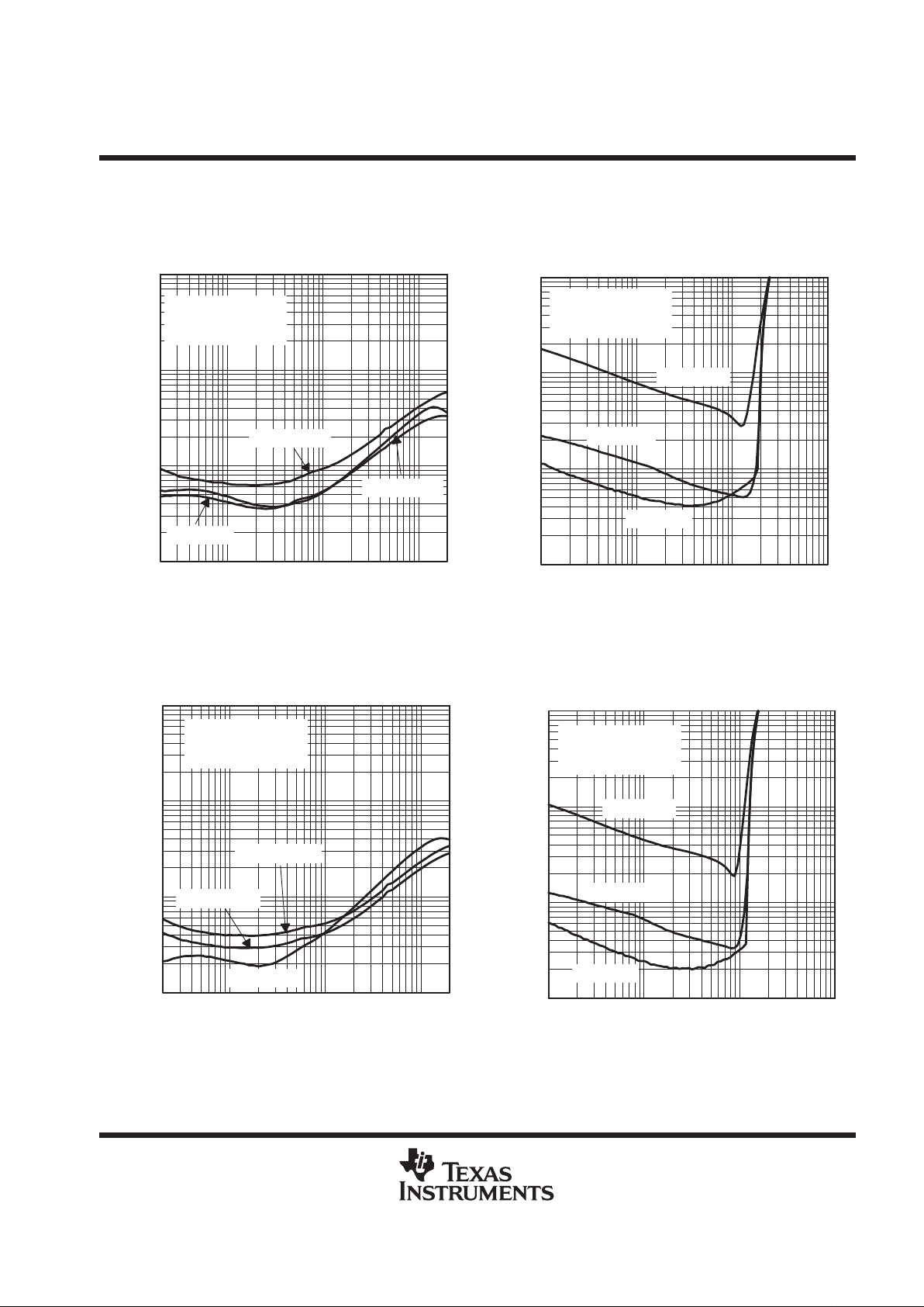
Figure 9
0.1%
0.01%
20
1%
10%
10k
f – Frequency – Hz
THD+N –Total Harmonic Distortion + Noise
TOTAL HARMONIC DISTORTION PLUS NOISE
vs
FREQUENCY
PO = 25 mW
20k
RL = 32 Ω
AV = +14 to 0 dB
SE
PO = 50 mW
PO = 75 mW
100 1k
0.001%
Figure 10
0.1%
0.01%
0.01 0.1
1%
10%
1
f = 20 Hz
f = 1 kHz
PO – Output Power – W
THD+N –Total Harmonic Distortion + Noise
TOTAL HARMONIC DISTORTION PLUS NOISE
vs
OUTPUT POWER
f = 20 kHz
RL = 32 Ω
AV = +14 to 0 dB
SE
Figure 11
0.001%
10%
20 100 1k 10k 20k
THD+N –Total Harmonic Distortion + Noise
f – Frequency – Hz
TOTAL HARMONIC DISTORTION PLUS NOISE
vs
FREQUENCY
1%
0.1%
VO = 1 V
RMS
0.01%
RL = 10 kΩ
AV = +14 to 0 dB
SE
Figure 12
THD+N –Total Harmonic Distortion + Noise
TOTAL HARMONIC DISTORTION PLUS NOISE
vs
OUTPUT VOLTAGE
PO = 20 kHz
VO – Output Voltage – V
RMS
0 0.2 0.4 0.6 0.8 1 1.2 1.4 1.6 1.8 2
0.001%
0.01%
0.1%
1%
10%
RL = 10 kΩ
AV = +14 to 0 dB
SE
PO = 1 kHz
PO = 20 Hz
TPA0132
2-W STEREO AUDIO POWER AMPLIFIER
WITH DC VOLUME CONTROL
SLOS223B – MAY 1999 – REVISED MARCH 2000
9
POST OFFICE BOX 655303 • DALLAS, TEXAS 75265
TYPICAL CHARACTERISTICS
Figure 13
120
0
0 100
140
160
1k 10k
f – Frequency – Hz
VDD = 5 V
BW = 22 Hz to 22 kHz
RL = 4 Ω
OUTPUT NOISE VOLTAGE
vs
FREQUENCY
AV = +20 dB
20k
AV = +6 dB
– Output Noise Voltage – VµV
n
RMS
20
40
60
80
100
Figure 14
–100
–120
20 100
–80
1k 10k
RL = 8 Ω
CB = 0.47 µF
BTL
Supply Ripple Rejection Ratio – dB
SUPPLY RIPPLE REJECTION RATIO
vs
FREQUENCY
AV = +6 dB
–60
–40
–20
0
f – Frequency – Hz
20k
AV = +20 dB
Figure 15
–100
–120
20 100
–80
1k 10k
RL = 32 Ω
CB = 0.47 µF
SE
SUPPLY RIPPLE REJECTION RATIO
vs
FREQUENCY
AV = +6 dB
–60
–40
–20
0
f – Frequency – Hz
20k
AV = +14 dB
Supply Ripple Rejection Ratio – dB
Figure 16
–120
–80
20 100 1k 10k 20k
Crosstalk – dB
f – Frequency – Hz
CROSSTALK
vs
FREQUENCY
–90
–100
–110
PO = 1 W
RL = 8 Ω
AV = +20 dB
BTL
–70
–60
LEFT TO RIGHT
RIGHT TO LEFT
–50
–40
TPA0132
2-W STEREO AUDIO POWER AMPLIFIER
WITH DC VOLUME CONTROL
SLOS223B – MAY 1999 – REVISED MARCH 2000
10
POST OFFICE BOX 655303 • DALLAS, TEXAS 75265
TYPICAL CHARACTERISTICS
Figure 17
–120
–80
20 100 1k 10k 20k
Crosstalk – dB
f – Frequency – Hz
CROSSTALK
vs
FREQUENCY
–90
–100
–110
PO = 1 W
RL = 8 Ω
AV = +60dB
BTL
–70
–60
LEFT TO RIGHT
RIGHT TO LEFT
–50
–40
Figure 18
–120
–40
20 100 1k 10k 20k
Crosstalk – dB
f – Frequency – Hz
CROSSTALK
vs
FREQUENCY
–60
–80
–100
VO = 1 V
RMS
RL = 10 kΩ
AV = +6 dB
SE
–20
0
LEFT TO RIGHT
RIGHT TO LEFT
Figure 19
–120
–40
20 100 1k 10k 20k
Shutdown Attenuation – dB
f – Frequency – Hz
SHUTDOWN ATTENUATION
vs
FREQUENCY
–60
–80
–100
–20
0
VI = 1 V
RMS
RL = 8 Ω, BTL
RL = 32 Ω, SE
RL = 10 kΩ, SE
Figure 20
80
110
0 100 1k 10k 20k
SNR – Signal-To-Noise Ratio – dB
f – Frequency – Hz
SIGNAL-TO-NOISE RATIO
vs
FREQUENCY
105
100
95
115
120
85
90
PO = 1 W
RL = 8 Ω
BTL
AV = +20 dB
AV = +6 dB

TPA0132
2-W STEREO AUDIO POWER AMPLIFIER
WITH DC VOLUME CONTROL
SLOS223B – MAY 1999 – REVISED MARCH 2000
11
POST OFFICE BOX 655303 • DALLAS, TEXAS 75265
TYPICAL CHARACTERISTICS
–10
20
10 100 1k 10k 100k
Gain – dB
f – Frequency – Hz
CLOSED LOOP RESPONSE
15
10
5
25
30
–5
0
180°
90°
0°
–90°
–180°
1M
Phase
RL = 8 Ω
AV = +20 dB
BTL
Gain
Phase
Figure 21
–10
20
10 100 1k 10k 100k
Gain – dB
f – Frequency – Hz
CLOSED LOOP RESPONSE
15
10
5
25
30
–5
0
180°
90°
0°
–90°
–180°
1M
RL = 8 Ω
AV = +6 dB
BTL
Gain
Phase
Phase
Figure 22
TPA0132
2-W STEREO AUDIO POWER AMPLIFIER
WITH DC VOLUME CONTROL
SLOS223B – MAY 1999 – REVISED MARCH 2000
12
POST OFFICE BOX 655303 • DALLAS, TEXAS 75265
TYPICAL CHARACTERISTICS
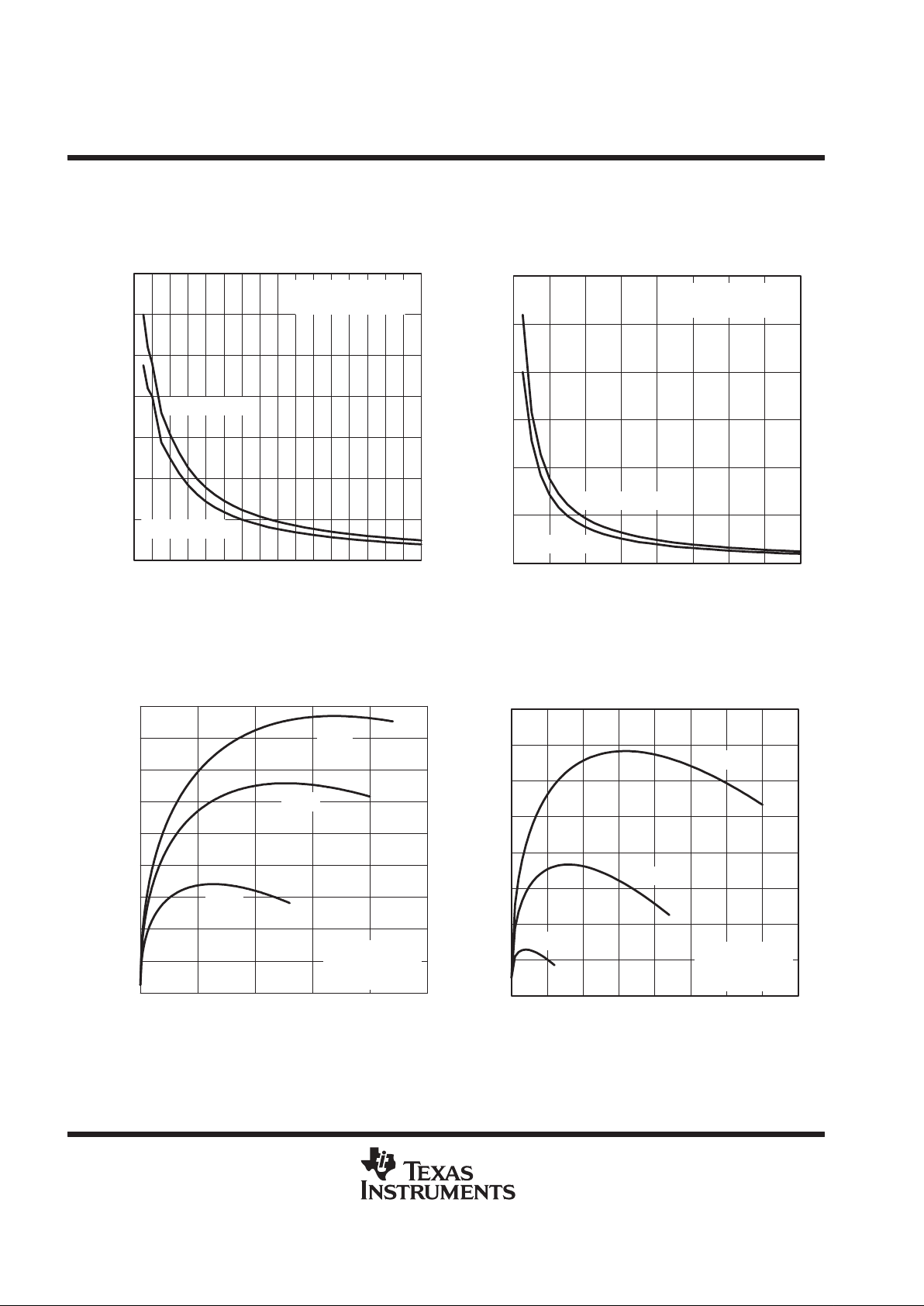
Figure 23
2
1.5
0
0816243240
2.5
3
3.5
48 56 64
RL – Load Resistance – Ω
AV = +20 to 0 dB
BTL
– Output Power – WP
O
OUTPUT POWER
vs
LOAD RESISTANCE
1% THD+N
10% THD+N
1
0.5
Figure 24
750
0
0816
1000
1250
1500
24 32
RL – Load Resistance – Ω
AV = +14 to 0 dB
SE
– Output Power – mWP
O
OUTPUT POWER
vs
LOAD RESISTANCE
1% THD+N
10% THD+N
500
250
40 48 56 64
Figure 25
0.6
0.4
0.2
0
01
– Power Dissipation – W
1
1.2
POWER DISSIPATION
vs
OUTPUT POWER
1.4
1.5 2.5
0.8
PO – Output Power – W
P
D
4 Ω
8 Ω
f = 1 kHz
BTL
Each Channel
3 Ω
1.6
1.8
0.5 2
Figure 26
0.1
0.05
0
0 0.2
– Power Dissipation – W
0.2
0.25
POWER DISSIPATION
vs
OUTPUT POWER
0.3
0.3 0.8
0.15
PO – Output Power – W
P
D
8 Ω
32 Ω
f = 1 kHz
BTL
Each Channel
4 Ω
0.35
0.4
0.1 0.70.4 0.5 0.6
TPA0132
2-W STEREO AUDIO POWER AMPLIFIER
WITH DC VOLUME CONTROL
SLOS223B – MAY 1999 – REVISED MARCH 2000
13
POST OFFICE BOX 655303 • DALLAS, TEXAS 75265
TYPICAL CHARACTERISTICS
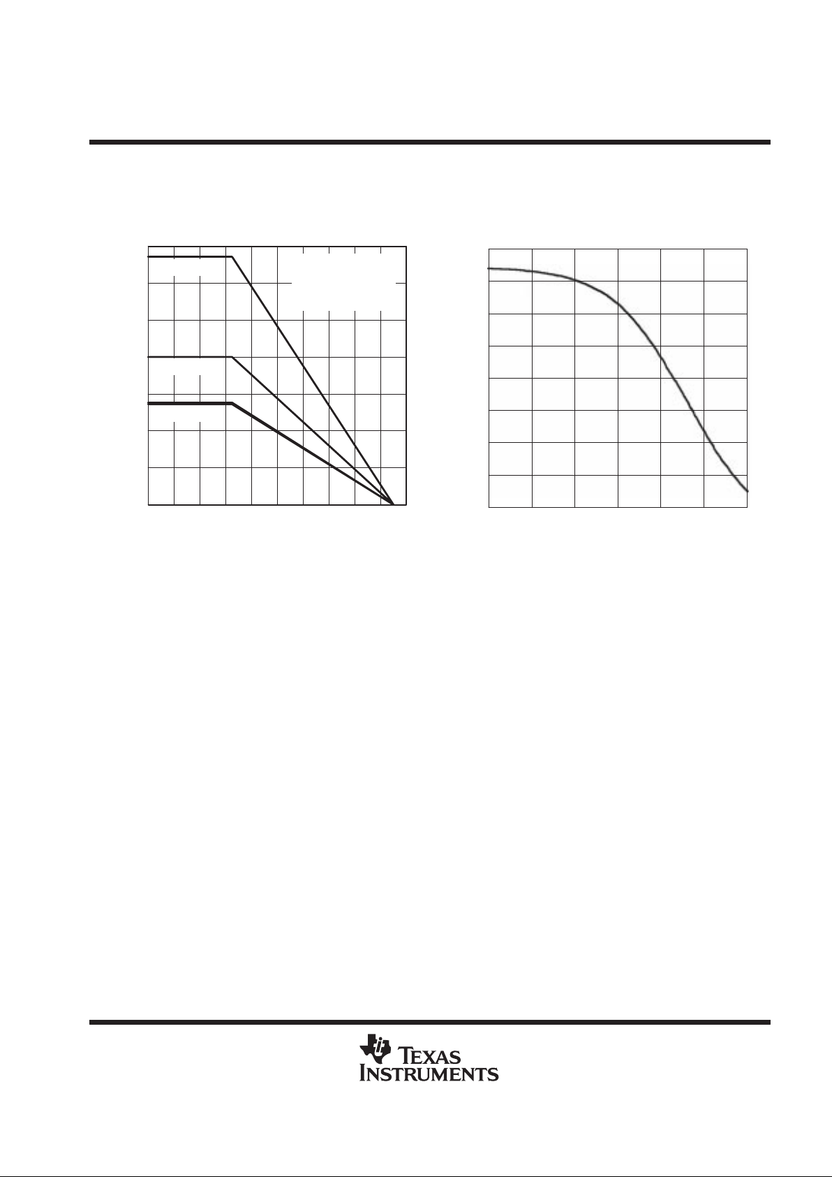
Figure 27
1
0
–40 0
– Power Dissipation – W
3
4
POWER DISSIPATION
vs
AMBIENT TEMPERATURE
5
20 160
2
TA – Ambient Temperature – °C
P
D
6
7
–20 10040 60 80 120 140
Θ
JA3
Θ
JA1,2
Θ
JA4
Θ
JA1
= 45.9°C/W
Θ
JA2
= 45.2°C/W
Θ
JA3
= 31.2°C/W
Θ
JA4
= 18.6°C/W
Figure 28
40
30
20
10
–40 –20
60
70
INPUT IMPEDANCE
vs
GAIN
80
–10 10
50
AV – Gain – dB
90
–30 0
20
– Input Impedance –Z
I
Ω

TPA0132
2-W STEREO AUDIO POWER AMPLIFIER
WITH DC VOLUME CONTROL
SLOS223B – MAY 1999 – REVISED MARCH 2000
14
POST OFFICE BOX 655303 • DALLAS, TEXAS 75265
APPLICATION INFORMATION
Table 1. DC Volume Control
VOLUME (Terminal 3)
FROM
(V)
TO
(V)
GAIN of AMPLIFIER
(dB)
0 0.15 20
0.15 0.28 18
0.28 0.39 16
0.39 0.5 14
0.5 0.61 12
0.61 0.73 10
0.73 0.84 8
0.84 0.95 6
0.95 1.06 4
1.06 1.17 2
1.17 1.28 0
1.28 1.39 –2
1.39 1.5 –4
1.5 1.62 –6
1.62 1.73 –8
1.73 1.84 –10
1.84 1.95 –12
1.95 2.07 –14
2.07 2.18 –16
2.18 2.29 –18
2.29 2.41 –20
2.41 2.52 –22
2.52 2.63 –24
2.63 2.74 –26
2.74 2.86 –28
2.86 2.97 –30
2.97 3.08 –32
3.08 3.2 –34
3.2 3.31 –36
3.31 3.42 –38
3.42 3.54 –40
3.54 5 –85
selection of components
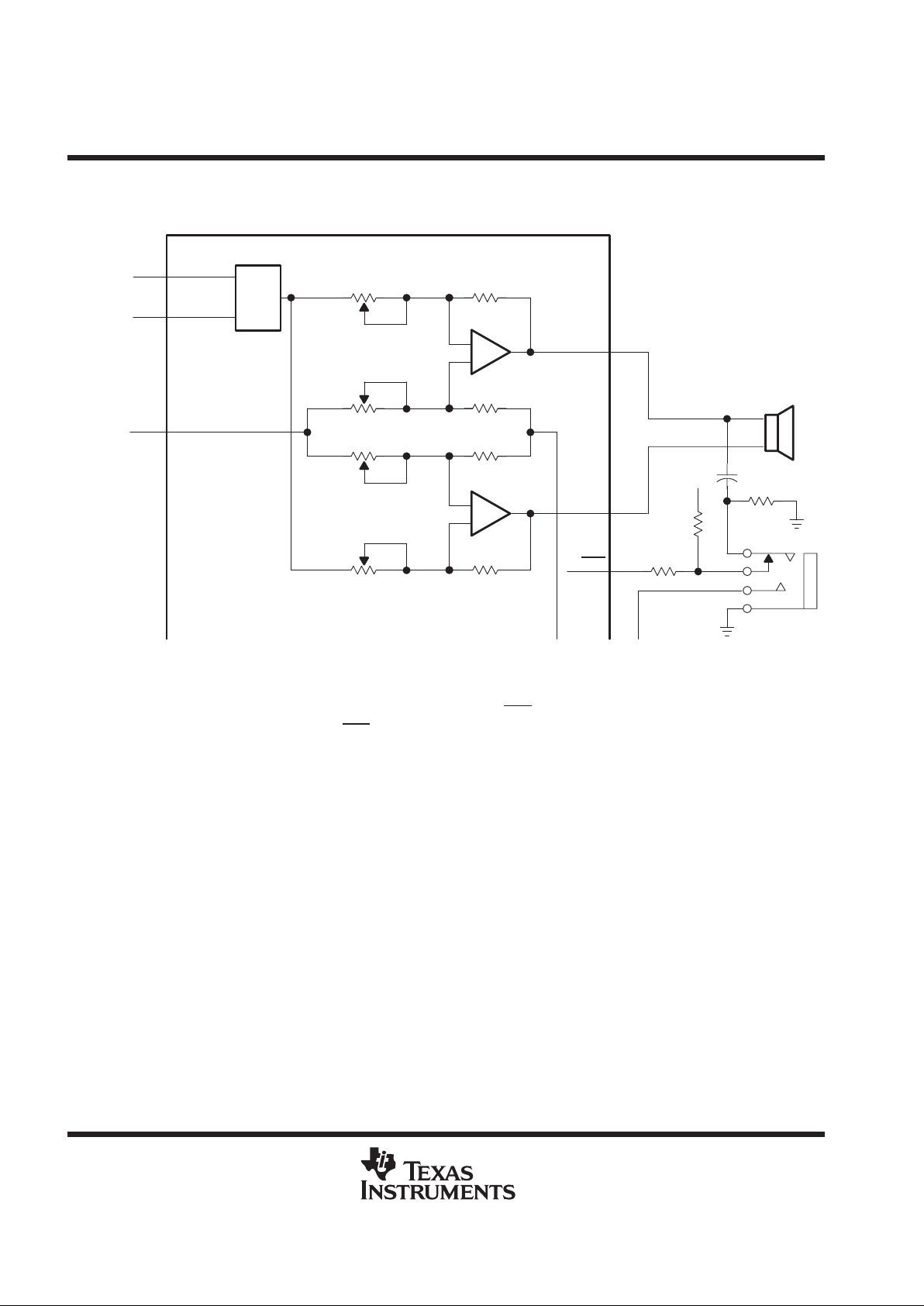
Figure 29 and Figure 30 are a schematic diagrams of typical notebook computer application circuits.

TPA0132
2-W STEREO AUDIO POWER AMPLIFIER
WITH DC VOLUME CONTROL
SLOS223B – MAY 1999 – REVISED MARCH 2000
15
POST OFFICE BOX 655303 • DALLAS, TEXAS 75265
APPLICATION INFORMATION
ROUT+ 21
R
MUX
RHPIN
RLINEIN
+
–
23
20
C
IRHP
0.47 µF
Right
Head–
phone
Input
Signal
C
IRLINE
0.47 µF
Right
Line
Input
Signal
C
RIN
0.47 µF
8 RIN
ROUT– 16
+
–
1 kΩ
C
OUTR
330 µF
100 kΩ
L
MUX
LHPIN
LLINEIN5
6
C
ILHP
0.47 µF
Left
Head–
phone
Input
Signal
C
ILLINE
0.47 µF
Left
Line
Input
Signal
C
LIN
0.47 µF
10 LIN
1 kΩ
C
OUTR
330 µF
V
DD
100 kΩ
Depop
Circuitry
Power
Management
PVDD 18
VDD 19
BYPASS 11
SHUT–
DOWN
22
GND
LOUT+ 4
+
–
LOUT– 9
+
–
C
BYP
0.47 µF
1,12,
13,24
To
System
Control
C
SR
0.1 µF
V
DD
C
SR
0.1 µF
V
DD
See Note A
PC–
Beep
PC–BEEP
PCB
ENABLE
14
C
PCB
0.47 µF
PC BEEP
Input
Signal
2
Gain/
MUX
Control
VOLUME
CLK
3
17
SE/BTL
15
C
CLK
47 nF
V
DD
50 kΩ
NOTE A: A 0.1 µF ceramic capacitor should be placed as close as possible to the IC. For filtering lower–frequency noise signals, a larger
electrolytic capacitor of 10 µF or greater should be placed near the audio power amplifier.
Figure 29. Typical TPA0132 Application Circuit Using Single-Ended Inputs and Input MUX

TPA0132
2-W STEREO AUDIO POWER AMPLIFIER
WITH DC VOLUME CONTROL
SLOS223B – MAY 1999 – REVISED MARCH 2000
16
POST OFFICE BOX 655303 • DALLAS, TEXAS 75265
APPLICATION INFORMATION
ROUT+ 21
R
MUX
RHPIN
RLINEIN
+
–
23
20
C
CRIN–
0.47 µF
8 RIN
ROUT– 16
+
–
1 kΩ
C
OUTR
330 µF
100 kΩ
L
MUX
LHPIN
LLINEIN5
6
C
IlHP
0.47 µF
Left
Head–
phone
Input
Signal
C
ILLINE
0.47 µF
Left
Line
Input
Signal
C
LIN
0.47 µF
10 LIN
1 kΩ
C
OUTR
330 µF
V
DD
100 kΩ
Depop
Circuitry
Power
Management
PVDD 18
VDD 19
BYPASS 11
SHUT–
DOWN
22
GND
LOUT+ 4
+
–
LOUT– 9
+
–
C
BYP
0.47 µF
1,12,
13,24
To
System
Control
C
SR
0.1 µF
V
DD
C
SR
0.1 µF
V
DD
See Note A
PC–
Beep
PC–BEEP
PCB
ENABLE
14
C
PCB
0.47 µF
PC BEEP
Input
Signal
2
Gain/
MUX
Control
VOLUME
CLK
3
1717
SE/BTL
15
N/C
C
RIN+
0.47 µF
Right
Positive
Differential
Input
Signal
Right
Negative
Differential
Input
Signal
C
CLK
47 nF
V
DD
50 kΩ
NOTE A: A 0.1 µF ceramic capacitor should be placed as close as possible to the IC. For filtering lower–frequency noise signals, a larger
electrolytic capacitor of 10 µF or greater should be placed near the audio power amplifier.
Figure 30. Typical TPA0132 Application Circuit Using Differential Inputs

TPA0132
2-W STEREO AUDIO POWER AMPLIFIER
WITH DC VOLUME CONTROL
SLOS223B – MAY 1999 – REVISED MARCH 2000
17
POST OFFICE BOX 655303 • DALLAS, TEXAS 75265
APPLICATION INFORMATION
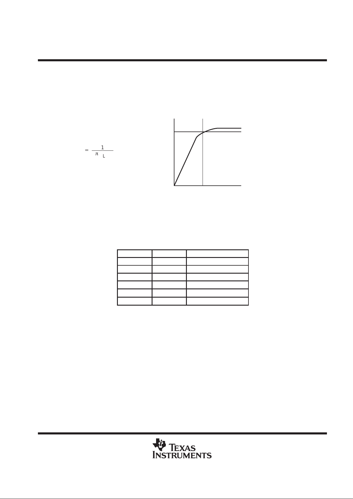
input resistance
Each gain setting is achieved by varying the input resistance of the amplifier, which can range from its smallest
value to over 6 times that value. As a result, if a single capacitor is used in the input high pass filter, the –3 dB
or cut-off frequency will also change by over 6 times. If an additional resistor is connected from the input pin
of the amplifier to ground, as shown in the figure below, the variation of the cut-off frequency will be much
reduced.
C
R
IN
R
I
R
f
Input Signal
Figure 31. Resistor on Input for Cut-Off Frequency
The input resistance at each gain setting is given in Figure 28.
The –3 dB frequency can be calculated using the following formula:
(1)
f
–3 dB
+
1
2pCǒRøR
I
Ǔ
If the filter must be more accurate, the value of the capacitor should be increased while value of the resistor to
ground should be decreased. In addition, the order of the filter could be increased.
input capacitor, C
I
In the typical application an input capacitor, C
I
, is required to allow the amplifier to bias the input signal to the
proper dc level for optimum operation. In this case, CI and the input impedance of the amplifier, ZI, form a
high-pass filter with the corner frequency determined in equation 2.
f
c(highpass)
+
1
2pZ
IN
C
I
–3 dB
f
c
(2)

TPA0132
2-W STEREO AUDIO POWER AMPLIFIER
WITH DC VOLUME CONTROL
SLOS223B – MAY 1999 – REVISED MARCH 2000
18
POST OFFICE BOX 655303 • DALLAS, TEXAS 75265
APPLICATION INFORMATION
input capacitor, C
I
(continued)
The value of CI is important to consider as it directly affects the bass (low frequency) performance of the circuit.
Consider the example where ZI is 710 kΩ and the specification calls for a flat bass response down to 40 Hz.
Equation 2 is reconfigured as equation 3.
CI+
1
2pZ
I
f
c
(3)
In this example, CI is 5.6 nF so one would likely choose a value in the range of 5.6 nF to 1 µF. A further
consideration for this capacitor is the leakage path from the input source through the input network (CI) and the
feedback network to the load. This leakage current creates a dc offset voltage at the input to the amplifier that
reduces useful headroom, especially in high gain applications. For this reason a low-leakage tantalum or
ceramic capacitor is the best choice. When polarized capacitors are used, the positive side of the capacitor
should face the amplifier input in most applications as the dc level there is held at VDD/2, which is likely higher
that the source dc level. Note that it is important to confirm the capacitor polarity in the application.
power supply decoupling, C
S
The TPA0132 is a high-performance CMOS audio amplifier that requires adequate power supply decoupling
to ensure the output total harmonic distortion (THD) is as low as possible. Power supply decoupling also
prevents oscillations for long lead lengths between the amplifier and the speaker. The optimum decoupling is
achieved by using two capacitors of different types that target different types of noise on the power supply leads.
For higher frequency transients, spikes, or digital hash on the line, a good low equivalent-series-resistance
(ESR) ceramic capacitor, typically 0.1 µF placed as close as possible to the device V
DD
lead works best. For
filtering lower-frequency noise signals, a larger aluminum electrolytic capacitor of 10 µF or greater placed near
the audio power amplifier is recommended.
midrail bypass capacitor, C
BYP
The midrail bypass capacitor, C
BYP
, is the most critical capacitor and serves several important functions. During
startup or recovery from shutdown mode, C
BYP
determines the rate at which the amplifier starts up. The second
function is to reduce noise produced by the power supply caused by coupling into the output drive signal. This
noise is from the midrail generation circuit internal to the amplifier, which appears as degraded PSRR and
THD+N.
Bypass capacitor, C
BYP
, values of 0.47 µF to 1 µF ceramic or tantalum low-ESR capacitors are recommended
for the best THD and noise performance.
TPA0132
2-W STEREO AUDIO POWER AMPLIFIER
WITH DC VOLUME CONTROL
SLOS223B – MAY 1999 – REVISED MARCH 2000
19
POST OFFICE BOX 655303 • DALLAS, TEXAS 75265
APPLICATION INFORMATION
output coupling capacitor, C
C
In the typical single-supply SE configuration, an output coupling capacitor (C
C
) is required to block the dc bias
at the output of the amplifier thus preventing dc currents in the load. As with the input coupling capacitor, the
output coupling capacitor and impedance of the load form a high-pass filter governed by equation 4.
(4)
f
c(high)
+
1
2pR
L
C
C
–3 dB
f
c
The main disadvantage, from a performance standpoint, is the load impedances are typically small, which drives
the low-frequency corner higher degrading the bass response. Large values of CC are required to pass low
frequencies into the load. Consider the example where a CC of 330 µF is chosen and loads vary from 3 Ω,
4 Ω, 8 Ω, 32 Ω, 10 kΩ, and 47 kΩ. Table 2 summarizes the frequency response characteristics of each
configuration.
Table 2. Common Load Impedances Vs Low Frequency Output Characteristics in SE Mode
R
L
C
C
Lowest Frequency
3 Ω 330 µF 161 Hz
4 Ω 330 µF 120 Hz
8 Ω 330 µF 60 Hz
32 Ω 330 µF
15 Hz
10,000 Ω 330 µF 0.05 Hz
47,000 Ω 330 µF 0.01 Hz
As Table 2 indicates, most of the bass response is attenuated into a 4-Ω load, an 8-Ω load is adequate,
headphone response is good, and drive into line level inputs (a home stereo for example) is exceptional.
using low-ESR capacitors
Low-ESR capacitors are recommended throughout this applications section. A real (as opposed to ideal)
capacitor can be modeled simply as a resistor in series with an ideal capacitor. The voltage drop across this
resistor minimizes the beneficial effects of the capacitor in the circuit. The lower the equivalent value of this
resistance the more the real capacitor behaves like an ideal capacitor.

TPA0132
2-W STEREO AUDIO POWER AMPLIFIER
WITH DC VOLUME CONTROL
SLOS223B – MAY 1999 – REVISED MARCH 2000
20
POST OFFICE BOX 655303 • DALLAS, TEXAS 75265
APPLICATION INFORMATION
bridged-tied load versus single-ended mode
Figure 32 shows a Class-AB audio power amplifier (AP A) in a BTL configuration. The TPA0132 BTL amplifier
consists of two Class-AB amplifiers driving both ends of the load. There are several potential benefits to this
differential drive configuration but initially consider power to the load. The differential drive to the speaker means
that as one side is slewing up, the other side is slewing down, and vice versa. This in effect doubles the voltage
swing on the load as compared to a ground referenced load. Plugging 2 × V
O(PP)
into the power equation, where
voltage is squared, yields 4× the output power from the same supply rail and load impedance (see equation 5).
Power
+
V
(rms)
2
R
L
(5)
V
(rms)
+
V
O(PP)
22
Ǹ
R
L
2x V
O(PP)
V
O(PP)
–V
O(PP)
V
DD
V
DD
Figure 32. Bridge-Tied Load Configuration

TPA0132
2-W STEREO AUDIO POWER AMPLIFIER
WITH DC VOLUME CONTROL
SLOS223B – MAY 1999 – REVISED MARCH 2000
21
POST OFFICE BOX 655303 • DALLAS, TEXAS 75265
APPLICATION INFORMATION
In a typical computer sound channel operating at 5 V, bridging raises the power into an 8-Ω speaker from a
singled-ended (SE, ground reference) limit of 250 mW to 1 W. In sound power that is a 6-dB improvement —
which is loudness that can be heard. In addition to increased power there are frequency response concerns.
Consider the single-supply SE configuration shown in Figure 33. A coupling capacitor is required to block the
dc offset voltage from reaching the load. These capacitors can be quite large (approximately 33 µF to 1000 µF)
so they tend to be expensive, heavy , occupy valuable PCB area, and have the additional drawback of limiting
low-frequency performance of the system. This frequency limiting effect is due to the high pass filter network
created with the speaker impedance and the coupling capacitance and is calculated with equation 6.
f
(c)
+
1
2pR
L
C
C
(6)
For example, a 68-µF capacitor with an 8-Ω speaker would attenuate low frequencies below 293 Hz. The BTL
configuration cancels the dc offsets, which eliminates the need for the blocking capacitors. Low-frequency
performance is then limited only by the input network and speaker response. Cost and PCB space are also
minimized by eliminating the bulky coupling capacitor.
R
L
C
C
V
O(PP)
V
O(PP)
V
DD
–3 dB
f
c
Figure 33. Single-Ended Configuration and Frequency Response
Increasing power to the load does carry a penalty of increased internal power dissipation. The increased
dissipation is understandable considering that the BTL configuration produces 4× the output power of the SE
configuration. Internal dissipation versus output power is discussed further in the
crest factor and thermal
considerations
section.
single-ended operation
In SE mode (see Figure 32 and Figure 33), the load is driven from the primary amplifier output for each channel
(OUT+, terminals 21 and 4).
The amplifier switches single-ended operation when the SE/BTL terminal is held high. This puts the negative
outputs in a high-impedance state, and reduces the amplifier’s gain to 1 V/V .
BTL amplifier efficiency
Class-AB amplifiers are notoriously inefficient. The primary cause of these inefficiencies is voltage drop across
the output stage transistors. There are two components of the internal voltage drop. One is the headroom or
dc voltage drop that varies inversely to output power. The second component is due to the sinewave nature of
the output. The total voltage drop can be calculated by subtracting the RMS value of the output voltage from
V
DD
. The internal voltage drop multiplied by the RMS value of the supply current, IDDrms, determines the internal
power dissipation of the amplifier.
TPA0132
2-W STEREO AUDIO POWER AMPLIFIER
WITH DC VOLUME CONTROL
SLOS223B – MAY 1999 – REVISED MARCH 2000
22
POST OFFICE BOX 655303 • DALLAS, TEXAS 75265
APPLICATION INFORMATION
An easy-to-use equation to calculate efficiency starts out as being equal to the ratio of power from the power
supply to the power delivered to the load. T o accurately calculate the RMS and average values of power in the
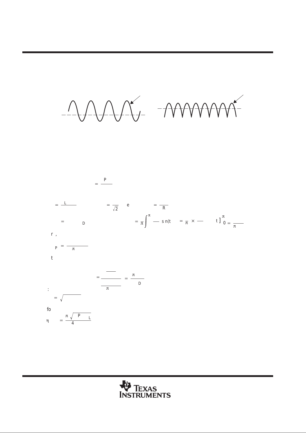
load and in the amplifier, the current and voltage waveform shapes must first be understood (see Figure 34).
V
(LRMS)
V
O
I
DD
I
DD(avg)
Figure 34. Voltage and Current Waveforms for BTL Amplifiers
Although the voltages and currents for SE and BTL are sinusoidal in the load, currents from the supply are very
different between SE and BTL configurations. In an SE application the current waveform is a half-wave rectified
shape whereas in BTL it is a full-wave rectified waveform. This means RMS conversion factors are different.
Keep in mind that for most of the waveform both the push and pull transistors are not on at the same time, which
supports the fact that each amplifier in the BTL device only draws current from the supply for half the waveform.
The following equations are the basis for calculating amplifier efficiency.
Efficiency of a BTL amplifier
+
P
L
P
SUP
(7)
Where:
(8)
PL+
V
L
rms
2
R
L
, andV
LRMS
+
V
P
2
Ǹ
, therefore, PL+
V
P
2
2R
L
PL = Power delivered to load
P
SUP
= Power drawn from power supply
V
LRMS
= RMS voltage on BTL load
R
L
= Load resistance
V
P
= Peak voltage on BTL load
I
DD
avg = Average current drawn from
the power supply
V
DD
= Power supply voltage
η
BTL
= Efficiency of a BTL amplifier
and
P
SUP
+
VDDIDDavg
and
IDDavg
+
1
p
ŕ
p
0
V
P
R
L
sin(t) dt
+
1
p
V
P
R
L
[cos(t)]
p
0
+
2V
P
p
R
L
Therefore,
P
SUP
+
2V
DDVP
p
R
L
substituting PL and P
SUP
into equation 7,
Efficiency of a BTL amplifier
+
V
P
2
2R
L
2VDDV
P
p
R
L
+
p
V
P
4V
DD
VP+
2PLR
L
Ǹ
h
BTL
+
p
2P
LRL
Ǹ
4V
DD
Where:
Therefore,
TPA0132
2-W STEREO AUDIO POWER AMPLIFIER
WITH DC VOLUME CONTROL
SLOS223B – MAY 1999 – REVISED MARCH 2000
23
POST OFFICE BOX 655303 • DALLAS, TEXAS 75265
APPLICATION INFORMATION
T able 3 employs equation 8 to calculate efficiencies for four different output power levels. Note that the efficiency
of the amplifier is quite low for lower power levels and rises sharply as power to the load is increased resulting
in a nearly flat internal power dissipation over the normal operating range. Note that the internal dissipation at
full output power is less than in the half power range. Calculating the efficiency for a specific system is the key
to proper power supply design. For a stereo 1-W audio system with 8-Ω loads and a 5-V supply , the maximum
draw on the power supply is almost 3.25 W.
Table 3. Efficiency Vs Output Power in 5-V 8-Ω BTL Systems
Output Power
(W)
Efficiency
(%)
Peak Voltage
(V)
Internal Dissipation
(W)
0.25 31.4 2.00 0.55
0.50 44.4 2.83 0.62
1.00 62.8 4.00 0.59
1.25 70.2 4.47
†
0.53
†
High peak voltages cause the THD to increase.
A final point to remember about Class-AB amplifiers (either SE or BTL) is how to manipulate the terms in the
efficiency equation to utmost advantage when possible. Note that in equation 8, VDD is in the denominator. This
indicates that as VDD goes down, efficiency goes up.
crest factor and thermal considerations
Class-AB power amplifiers dissipate a significant amount of heat in the package under normal operating
conditions. A typical music CD requires 12 dB to 15 dB of dynamic range, or headroom above the average power
output, to pass the loudest portions of the signal without distortion. In other words, music typically has a crest
factor between 12 dB and 15 dB. When determining the optimal ambient operating temperature the internal
dissipated power at the average output power level must be used. From the TP A0132 data sheet, one can see
that when the TPA0132 is operating from a 5-V supply into a 3-Ω speaker that 4 W peaks are available.
Converting watts to dB:
P
dB
+
10Log
P
W
P
ref
+
10Log
4W
1W
+
6dB
(9)
Subtracting the headroom restriction to obtain the average listening level without distortion yields:
6 dB – 15 dB = –9 dB (15 dB crest factor)
6 dB – 12 dB = –6 dB (12 dB crest factor)
6 dB – 9 dB = –3 dB (9 dB crest factor)
6 dB – 6 dB = 0 dB (6 dB crest factor)
6 dB – 3 dB = 3 dB (3 dB crest factor)
TPA0132
2-W STEREO AUDIO POWER AMPLIFIER
WITH DC VOLUME CONTROL
SLOS223B – MAY 1999 – REVISED MARCH 2000
24
POST OFFICE BOX 655303 • DALLAS, TEXAS 75265
APPLICATION INFORMATION
Converting dB back into watts:
P
W
+
10
PdBń10
P
ref
+
63 mW (18 dB crest factor)
+
125 mW (15 dB crest factor)
+
250 mW (9 dB crest factor)
+
500 mW (6 dB crest factor)
+
1000 mW (3 dB crest factor)
(10)
+
2000 mW (15 dB crest factor)
This is valuable information to consider when attempting to estimate the heat dissipation requirements for the
amplifier system. Comparing the absolute worst case, which is 2 W of continuous power output with a 3 dB crest
factor, against 12 dB and 15 dB applications drastically af fects maximum ambient temperature ratings for the
system. Using the power dissipation curves for a 5-V , 3-Ω system, the internal dissipation in the TPA0132 and
maximum ambient temperatures is shown in Table 4.
Table 4. TPA0132 Power Rating, 5-V, 3-Ω, Stereo
PEAK OUTPUT POWER
(W)
AVERAGE OUTPUT POWER
POWER DISSIPATION
(W/Channel)
MAXIMUM AMBIENT
TEMPERATURE
4 2 W (3 dB) 1.7 –3°C
4 1000 mW (6 dB) 1.6 6°C
4 500 mW (9 dB) 1.4 24°C
4 250 mW (12 dB) 1.1 51°C
4 125 mW (15 dB) 0.8 78°C
4 63 mW (18 dB) 0.6 96°C
Table 5. TPA0132 Power Rating, 5-V, 8-Ω, Stereo
PEAK OUTPUT POWER AVERAGE OUTPUT POWER
POWER DISSIPATION
(W/Channel)
MAXIMUM AMBIENT
TEMPERATURE
2.5 W 1250 mW (3 dB crest factor) 0.55 100°C
2.5 W 1000 mW (4 dB crest factor) 0.62 94°C
2.5 W 500 mW (7 dB crest factor) 0.59 97°C
2.5 W 250 mW (10 dB crest factor) 0.53 102°C
The maximum dissipated power, P
Dmax
, is reached at a much lower output power level for an 8 Ω load than for
a 3 Ω load. As a result, this simple formula for calculating P
Dmax
may be used for an 8 Ω application:
P
Dmax
+
2V
2
DD
p2R
L
(11)
However, in the case of a 3 Ω load, the P
Dmax
occurs at a point well above the normal operating power level.
The amplifier may therefore be operated at a higher ambient temperature than required by the P
Dmax
formula
for a 3 Ω load.

TPA0132
2-W STEREO AUDIO POWER AMPLIFIER
WITH DC VOLUME CONTROL
SLOS223B – MAY 1999 – REVISED MARCH 2000
25
POST OFFICE BOX 655303 • DALLAS, TEXAS 75265
APPLICATION INFORMATION
The maximum ambient temperature depends on the heat sinking ability of the PCB system. The derating factor
for the PWP package is shown in the dissipation rating table (see page 4). Converting this to ΘJA:
Θ
JA
+
1
Derating Factor
+
1
0.022
+
45°CńW
(12)
To calculate maximum ambient temperatures, first consider that the numbers from the dissipation graphs are
per channel so the dissipated power needs to be doubled for two channel operation. Given ΘJA, the maximum
allowable junction temperature, and the total internal dissipation, the maximum ambient temperature can be
calculated with the following equation. The maximum recommended junction temperature for the TP A0132 is
150°C. The internal dissipation figures are taken from the Power Dissipation vs Output Power graphs.
T
A
Max+TJMax
*
Θ
JAPD
+
150*45(0.6 2)+
96°C(15 dB crest factor
)
(13)
NOTE:
Internal dissipation of 0.6 W is estimated for a 2-W system with 15 dB crest factor per channel.
Tables 4 and 5 show that for some applications no airflow is required to keep junction temperatures in the
specified range. The TPA0132 is designed with thermal protection that turns the device off when the junction
temperature surpasses 150°C to prevent damage to the IC. T able 4 and 5 were calculated for maximum listening
volume without distortion. When the output level is reduced the numbers in the table change significantly . Also,
using 8-Ω speakers dramatically increases the thermal performance by increasing amplifier efficiency.
SE/BTL operation
The ability of the TP A0132 to easily switch between BTL and SE modes is one of its most important cost saving
features. This feature eliminates the requirement for an additional headphone amplifier in applications where
internal stereo speakers are driven in BTL mode but external headphone or speakers must be accommodated.
Internal to the TPA0132, two separate amplifiers drive OUT+ and OUT–. The SE/BTL
input (terminal 15)
controls the operation of the follower amplifier that drives LOUT– and ROUT– (terminals 9 and 16). When
SE/BTL
is held low, the amplifier is on and the TP A0132 is in the BTL mode. When SE/BTL is held high, the OUT–
amplifiers are in a high output impedance state, which configures the TPA0132 as an SE driver from LOUT+
and ROUT+ (terminals 4 and 21). IDD is reduced by approximately one-half in SE mode. Control of the SE/BTL
input can be from a logic-level CMOS source or, more typically, from a resistor divider network as shown in
Figure 35.
TPA0132
2-W STEREO AUDIO POWER AMPLIFIER
WITH DC VOLUME CONTROL
SLOS223B – MAY 1999 – REVISED MARCH 2000
26
POST OFFICE BOX 655303 • DALLAS, TEXAS 75265
APPLICATION INFORMATION
ROUT+ 21
R
MUX
RHPIN
RLINEIN
+
–
23
20
8 RIN
ROUT– 16
+
–
1 kΩ
C
OUTR
330 µF
100 kΩ
SE/BTL
15
100 kΩ
V
DD
Figure 35. TPA0132 Resistor Divider Network Circuit
Using a readily available 1/8-in. (3.5 mm) stereo headphone jack, the control switch is closed when no plug is
inserted. When closed the 100-kΩ/1-kΩ divider pulls the SE/BTL input low. When a plug is inserted, the 1-kΩ
resistor is disconnected and the SE/BTL
input is pulled high. When the input goes high, the OUT– amplifier is
shutdown causing the speaker to mute (virtually open-circuits the speaker). The OUT+ amplifier then drives
through the output capacitor (CO) into the headphone jack.
PC BEEP operation
The PC BEEP input allows a system beep to be sent directly from a computer through the amplifier to the
speakers with few external components. The input is normally activated activated automatically, but may be
selected manually by pulling PCB ENABLE high. When the PC BEEP input is active, both of the LINEIN and
HPIN inputs are deselected and both the left and right channels are driven in BTL mode with the signal from
PC BEEP . The gain from the PC BEEP input to the speakers is fixed at 0.3 V/V and is independent of the volume
setting. When the PC BEEP input is deselected, the amplifier will return to the previous operating mode and
volume setting. Furthermore, if the amplifier is in shutdown mode, activating PC BEEP will take the device out
of shutdown and output the PC BEEP signal, then return the amplifier to shutdown mode.
When PCB ENABLE is held low, the amplifier will automatically switch to PC BEEP mode after detecting a valid
signal at the PC BEEP input. The preferred input signal is a square wave or pulse train with an amplitude of 1
V
pp
or greater. To be a accurately detected, the signal must have a minimum of 1 Vpp amplitude, rise and fall
times of less than 0.1 µs and a minimum of 8 rising edges. When the signal is no longer detected, the amplifier
will return to its previous operating mode and volume setting.

TPA0132
2-W STEREO AUDIO POWER AMPLIFIER
WITH DC VOLUME CONTROL
SLOS223B – MAY 1999 – REVISED MARCH 2000
27
POST OFFICE BOX 655303 • DALLAS, TEXAS 75265
APPLICATION INFORMATION
When PCB ENABLE is held high, PC BEEP is selected and the LINEIN and HPIN inputs are deactivated
regardless of the input signal. PCB ENABLE has an internal 100 kΩ pulldown resistor and will trip at
approximately V
DD
/2.
If it is desired to ac couple the PC BEEP input, the value of the coupling capacitor should be chosen to satisfy
the following equation:
C
PCB
w
1
2pf
PCB
(100 kW)
(14)
The PC BEEP input can also be dc coupled to avoid using this coupling capacitor. The pin normally sits at midrail
when no signal is present.
Input MUX operation
ROUT+ 21
R
MUX
RHPIN
RLINEIN
+
–
23
20
C
IRHP
0.47 µF
Right
Headphone
Input
Signal
C
IRLINE
0.47 µF
Right Line
Input
Signal
C
RIN
0.47 µF
8 RIN
ROUT– 16
+
–
Figure 36. TPA0132 Example Input MUX Circuit
Another advantage of using the MUX feature is setting the gain of the headphone channel to –1. This provides
the optimum distortion performance into the headphones where clear sound is more important. Refer to the
SE/BTL
operation section for a description of the headphone jack control circuit.

TPA0132
2-W STEREO AUDIO POWER AMPLIFIER
WITH DC VOLUME CONTROL
SLOS223B – MAY 1999 – REVISED MARCH 2000
28
POST OFFICE BOX 655303 • DALLAS, TEXAS 75265
APPLICATION INFORMATION
shutdown modes
The TP A0132 employs a shutdown mode of operation designed to reduce supply current, IDD, to the absolute
minimum level during periods of nonuse for battery-power conservation. The SHUTDOWN input terminal
should be held high during normal operation when the amplifier is in use. Pulling SHUTDOWN low causes the
outputs to mute and the amplifier to enter a low-current state, IDD = 150 µA. SHUTDOWN should never be left
unconnected because amplifier operation would be unpredictable.
Table 6. Shutdown and Mute Mode Functions
INPUTS
†
AMPLIFIER STATE
SE/BTL SHUTDOWN INPUT OUTPUT
Low High Line BTL
X Low X Mute
High High HP SE
†
Inputs should never be left unconnected.
X = do not care

TPA0132
2-W STEREO AUDIO POWER AMPLIFIER
WITH DC VOLUME CONTROL
SLOS223B – MAY 1999 – REVISED MARCH 2000
29
POST OFFICE BOX 655303 • DALLAS, TEXAS 75265
MECHANICAL DATA
PWP (R-PDSO-G**) PowerPAD PLASTIC SMALL-OUTLINE PACKAGE
4073225/E 03/97
0,50
0,75
0,25
0,15 NOM
Thermal Pad
(See Note D)
Gage Plane
2824
7,70
7,90
20
6,40
6,60
9,60
9,80
6,60
6,20
11
0,19
4,50
4,30
10
0,15
20
A
1
0,30
1,20 MAX
1614
5,10
4,90
PINS **
4,90
5,10
DIM
A MIN
A MAX
0,05
Seating Plane
0,65
0,10
M
0,10
0°–8°
20-PIN SHOWN
NOTES: A. All linear dimensions are in millimeters.
B. This drawing is subject to change without notice.
C. Body dimensions do not include mold flash or protrusions.
D. The package thermal performance may be enhanced by bonding the thermal pad to an external thermal plane. This pad is electrically
and thermally connected to the backside of the die and terminals 1, 12, 13, and 24. The dimensions of the thermal pad are
2.40 mm × 4.70 mm (maximum). The pad is centered on the bottom of the package.
E. Falls within JEDEC MO-153
PowerPAD is a trademark of Texas Instruments Incorporated.

IMPORTANT NOTICE
T exas Instruments and its subsidiaries (TI) reserve the right to make changes to their products or to discontinue
any product or service without notice, and advise customers to obtain the latest version of relevant information
to verify, before placing orders, that information being relied on is current and complete. All products are sold
subject to the terms and conditions of sale supplied at the time of order acknowledgement, including those
pertaining to warranty, patent infringement, and limitation of liability.
TI warrants performance of its semiconductor products to the specifications applicable at the time of sale in
accordance with TI’s standard warranty. Testing and other quality control techniques are utilized to the extent
TI deems necessary to support this warranty. Specific testing of all parameters of each device is not necessarily
performed, except those mandated by government requirements.
CERT AIN APPLICATIONS USING SEMICONDUCTOR PRODUCTS MAY INVOLVE POTENTIAL RISKS OF
DEATH, PERSONAL INJURY, OR SEVERE PROPERTY OR ENVIRONMENTAL DAMAGE (“CRITICAL
APPLICATIONS”). TI SEMICONDUCTOR PRODUCTS ARE NOT DESIGNED, AUTHORIZED, OR
WARRANTED TO BE SUITABLE FOR USE IN LIFE-SUPPORT DEVICES OR SYSTEMS OR OTHER
CRITICAL APPLICATIONS. INCLUSION OF TI PRODUCTS IN SUCH APPLICA TIONS IS UNDERSTOOD T O
BE FULLY AT THE CUSTOMER’S RISK.
In order to minimize risks associated with the customer’s applications, adequate design and operating
safeguards must be provided by the customer to minimize inherent or procedural hazards.
TI assumes no liability for applications assistance or customer product design. TI does not warrant or represent
that any license, either express or implied, is granted under any patent right, copyright, mask work right, or other
intellectual property right of TI covering or relating to any combination, machine, or process in which such
semiconductor products or services might be or are used. TI’s publication of information regarding any third
party’s products or services does not constitute TI’s approval, warranty or endorsement thereof.
Copyright 2000, Texas Instruments Incorporated
 Loading...