


www.ti.com
1
2
3
4
5
6
7
8
9
10
11
12
24
23
22
21
20
19
18
17
16
15
14
13
PWP PACKAGE
(TOP VIEW)
GND
VOLUME
LOUT+
LLINEIN
LHPIN
PV
DD
RIN
LOUT–
LIN
BYPASS
GND
GND
RLINEIN
SHUTDOWN
ROUT+
RHPIN
V
DD
PV
DD
CLK
ROUT–
SE/BTL
PC-BEEP
GND
2.8-W STEREO AUDIO POWER AMPLIFIER
WITH DC VOLUME CONTROL
FEATURES
• Compatible With PC 99 Desktop Line-Out Into
10-k Ω Load
• Compatible With PC 99 Portable Into 8- Ω Load
• Internal Gain Control, Which Eliminates
External Gain-Setting Resistors
• DC Volume Control From 20 dB to -40 dB
• 2.8-W/Ch Output Power Into a 3- Ω Load
• PC-Beep Input
• Depop Circuitry
• Stereo Input MUX
• Fully Differential Input
• Low Supply Current and Shutdown Current
• Surface-Mount Power Packaging 24-Pin
TSSOP PowerPAD™
TPA0132
SLOS223E – MAY 1999 – REVISED SEPTEMBER 2004
DESCRIPTION
The TPA0132 is a stereo audio power amplifier in a 24-pin TSSOP thermally enhanced package capable of
delivering 2.8 W of continuous RMS power per channel into 3- Ω loads.
This device minimizes the number of external components needed, which simplifies the design and frees up
board space for other features. When driving 1 W into 8- Ω speakers, the TPA0132 has less than 0.4% THD+N
across its specified frequency range. Included within this device is integrated depop circuitry that virtually
eliminates transients that cause noise in the speakers.
Amplifier gain is controlled by means of a dc voltage input on the VOLUME terminal. There are 31 discrete steps
covering the range of 20 dB (maximum volume setting) to -40 dB (minimum volume setting) in 2-dB steps. When
the VOLUME terminal exceeds 3.54 V, the device is muted. An internal input MUX allows two sets of stereo
inputs to the amplifier. In notebook applications, where internal speakers are driven as bridge-tied load (BTL) and
the line outputs (often headphone drive) are required to be single-ended (SE), the TPA0132 automatically
switches into SE mode when the SE/ BTL input is activated, and this effectively reduces the gain by 6 dB.
The TPA0132 consumes only 10 mA of supply current during normal operation. A shutdown mode is included
that reduces the supply current to 150 µA.
The PowerPAD package (PWP) delivers a level of thermal performance that was previously achievable only in
TO-220-type packages. Thermal impedances of approximately 35 ° C/W are readily realized in multilayer PCB
applications. This allows the TPA0132 to operate at full power into 8- Ω loads at ambient temperatures of 85 ° C.
Please be aware that an important notice concerning availability, standard warranty, and use in critical applications of Texas
Instruments semiconductor products and disclaimers thereto appears at the end of this data sheet.
PowerPAD is a trademark of Texas Instruments.
PRODUCTION DATA information is current as of publication date.
Products conform to specifications per the terms of the Texas
Instruments standard warranty. Production processing does not
necessarily include testing of all parameters.
Copyright © 1999–2004, Texas Instruments Incorporated
www.ti.com
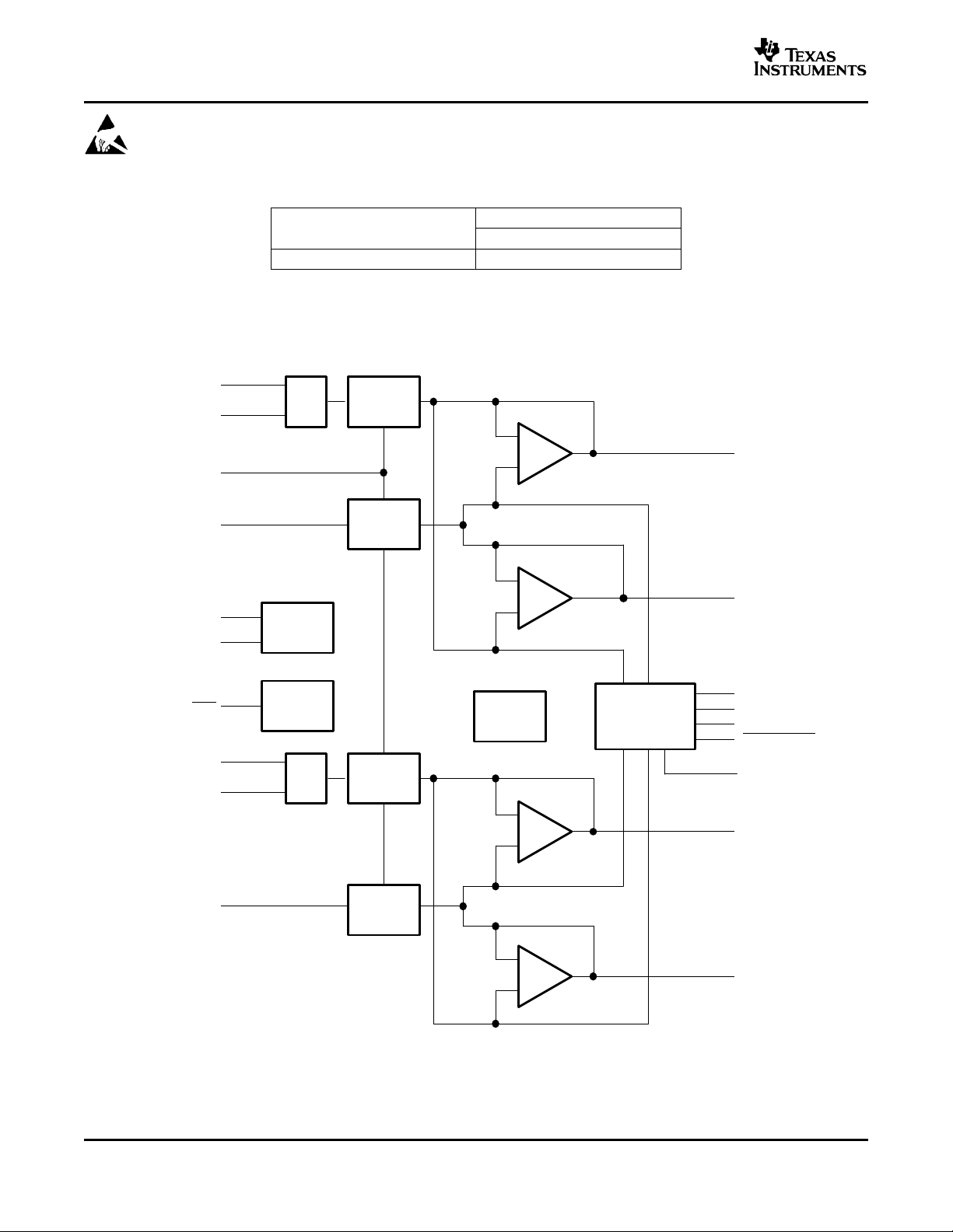
ROUT+
-
+
-
+
R
MUX
32-Step
Volume
Control
PC
Beep
MUX
Control
Depop
Circuitry
Power
Management
-
+
-
+
L
MUX
32-Step
Volume
Control
RHPIN
RLINEIN
VOLUME
RIN
PC-BEEP
SE/BTL
LHPIN
LLINEIN
LIN
ROUT-
PV
DD
V
DD
BYPASS
SHUTDOWN
GND
LOUT+
LOUT-
32-Step
Volume
Control
32-Step
Volume
Control
TPA0132
SLOS223E – MAY 1999 – REVISED SEPTEMBER 2004
These devices have limited built-in ESD protection. The leads should be shorted together or the device
placed in conductive foam during storage or handling to prevent electrostatic damage to the MOS gates.
(1) The PWP package is available taped and reeled. To order a taped
ORDERING INFORMATION
T
A
-40 ° C to 85 ° C TPA0132PWP
and reeled part, add the suffix R to the part number (e.g.,
TPA0132PWPR).
PACKAGED DEVICE
TSSOP (PWP)
FUNCTIONAL BLOCK DIAGRAM
(1)
2
www.ti.com
TPA0132
SLOS223E – MAY 1999 – REVISED SEPTEMBER 2004
Terminal Functions
TERMINAL
NAME NO.
BYPASS 11 Tap to voltage divider for internal mid-supply bias generator
CLK 17 I
GND I Ground connection for circuitry. Connected to thermal pad
1, 12
13, 24
LHPIN 6 I Left channel headphone input, selected when SE/ BTL is held high
LIN 10 I Common left input for fully differential input. AC ground for single-ended inputs.
LLINEIN 5 I Left channel line negative input, selected when SE/ BTL is held low
LOUT+ 4 O Left channel positive output in BTL mode and positive output in SE mode
LOUT- 9 O Left channel negative output in BTL mode and high-impedance in SE mode
PCB ENABLE 2 I the amplifier, regardless of its amplitude. If PCB ENABLE is floating or low, the amplifier continues to
PC-BEEP 14 I
PV
DD
7, 18 I Power supply for output stage
RHPIN 20 I Right channel headphone input, selected when SE/ BTL is held high
RIN 8 I Common right input for fully differential input. AC ground for single-ended inputs.
RLINEIN 23 I Right channel line input, selected when SE/ BTL is held low
ROUT+ 21 O Right channel positive output in BTL mode and positive output in SE mode
ROUT- 16 O Right channel negative output in BTL mode and high-impedance in SE mode
SE/ BTL 15 I
SHUTDOWN 22 I
V
DD
19 I
VOLUME 3 I of 20 dB to -40 dB for dc levels of 0.15 V to 3.54 V. When the dc level is over 3.54 V, the device is
Thermal Pad Connect to ground. Must be soldered down in all applications to properly secure device on PC board.
I/O DESCRIPTION
If a 47-nF capacitor is attached, the TPA0132 generates an internal clock. An external clock can
override the internal clock input to this terminal.
If this terminal is high, the detection circuitry for PC-BEEP is overridden and passes PC-BEEP through
operate normally.
The input for PC-Beep mode. PC-BEEP is enabled when a > 1.5-V (peak-to-peak) square wave is
input to PC-BEEP or PCB ENABLE is high.
Input and output MUX control. When this terminal is held high, the LHPIN or RHPIN and SE output is
selected. When this terminal is held low, the LLINEIN or RLINEIN and BTL output are selected.
When held low, this terminal places the entire device, except PC-BEEP detect circuitry, in shutdown
mode.
Analog V
performance.
input supply. This terminal needs to be isolated from PV
DD
to achieve highest
DD
VOLUME detects the dc level at the terminal and sets the gain for 31 discrete steps covering a range
muted.
ABSOLUTE MAXIMUM RATINGS
(1)
over operating free-air temperature range (unless otherwise noted)
Supply voltage, V
Input voltage, V
DD
I
Continuous total power dissipation Internally limited (see Dissipation Rating Table)
Operating free-air temperature range, T
Operating junction temperature range, T
Storage temperature range, T
stg
A
J
Lead temperature 1,6 mm (1/16 inch) from case for 10 seconds 260 ° C
(1) Stresses beyond those listed under "absolute maximum ratings” may cause permanent damage to the device. These are stress ratings
only, and functional operation of the device at these or any other conditions beyond those indicated under "recommended operating
conditions” is not implied. Exposure to absolute-maximum-rated conditions for extended periods may affect device reliability.
-0.3 V to V
-40 ° C to 85 ° C
-40 ° C to 150 ° C
-65 ° C to 85 ° C
6 V
0.3 V
DD
3
www.ti.com
TPA0132
SLOS223E – MAY 1999 – REVISED SEPTEMBER 2004
PACKAGE TA≤ 25 ° C DERATING FACTOR TA= 70 ° C TA= 85 ° C
PWP 2.7 W
(1) See the Texas Instruments document, PowerPAD Thermally Enhanced Package Application Report
(SLMA002), for more information on the PowerPAD™ package. The thermal data was measured on
a PCB layout based on the information in the section entitled Texas Instruments Recommended
Board for PowerPAD™ on page 33 of the before mentioned document.
RECOMMENDED OPERATING CONDITIONS
Supply voltage, V
High-level input voltage, V
Low-level input voltage, V
Operating free-air temperature, T
DD
IH
IL
A
DISSIPATION RATING TABLE
(1)
SE/ BTL 0.8 × V
SHUTDOWN 2 V
PCB ENABLE 0.6 × V
SE/ BTL 0.6 × V
SHUTDOWN 0.8 V
PCB ENABLE 0.4 × V
21.8 mW/ ° C 1.7 W 1.4 W
MIN MAX UNIT
4.5 5.5 V
DD
DD
DD
DD
-40 85 ° C
ELECTRICAL CHARACTERISTICS
at specified free-air temperature, V
PARAMETER TEST CONDITIONS MIN TYP MAX UNIT
|V
| Output offset voltage (measured differentially) VI= 0 V, AV= 6 dB 35 mV
OO
PSRR Power supply rejection ratio V
|IIH|
|IIL| V
I
DD
I
DD(SD)
High-level input current - SHUTDOWN, SE/ BTL, VOLUME V
High-level input current - PCB ENABLE V
Low-level input current - SHUTDOWN, SE/ BTL, VOLUME,
PCB ENABLE
Supply current mA
Supply current, shutdown mode SHUTDOWN = 0 V, SE/ BTL = 0 V 150 300 µA
= 5 V, TA= 25 ° C (unless otherwise noted)
DD
= 4.9 V to 5.1 V 67 dB
DD
= 5.5 V, VI= V
DD
= 5.5 V, VI= V
DD
= 5.5 V, VI= 0 V 900 nA
DD
DD
DD
BTL mode, SHUTDOWN = 2 V,
SE/ BTL = 0.6 × V
DD
SE mode, SHUTDOWN = 2 V,
SE/ BTL = 0.8 × V
DD
OPERATING CHARACTERISTICS
V
= 5 V, TA= 25 ° C, RL= 4 Ω , Gain = 2 V/V, BTL mode (unless otherwise noted)
DD
PARAMETER TEST CONDITIONS MIN TYP MAX UNIT
P
Output power RL= 3 Ω , f = 1 kHz
O
THD+N Total harmonic distortion plus noise PO= 1 W, f = 20 Hz to 15 kHz 0.4%
B
V
Maximum output power bandwidth THD = 5% >15 kHz
OM
Supply ripple rejection ratio dB
Noise output voltage µV
n
f = 1 kHz,
C
= 0.47 µF
(BYP)
C
= 0.47 µF,
(BYP)
f = 20 Hz to 20 kHz
THD = 10% 2.8 W
THD = 1% 2.3 W
BTL mode -65
SE mode -60
BTL mode 42
SE mode 44
900 nA
125 µA
10 15
5 7.5
RMS
4
www.ti.com
0.01%
-40 -30 -20 -10 0
THD+N -Total Harmonic Distortion + Noise
A - V oltage Gain - dB
1%
0.1%
10 20
V
PO = 1 W for A
V
≥ 6 dB
V
O
= 1 V
RMS
for A
V
≤ 4 dB
RL = 8 Ω
BTL
0.1%
0.01%
0.5 0.75 1 1.25 1.5 1.75 2
1%
10%
2.25 2.5 2.75 3
PO - Output Power - W
AV = 20 to 0 dB
f = 1 kHz
BTL
THD+N -Total Harmonic Distortion + Noise
RL = 8 Ω
RL = 3 Ω
RL = 4 Ω
SLOS223E – MAY 1999 – REVISED SEPTEMBER 2004
TYPICAL CHARACTERISTICS
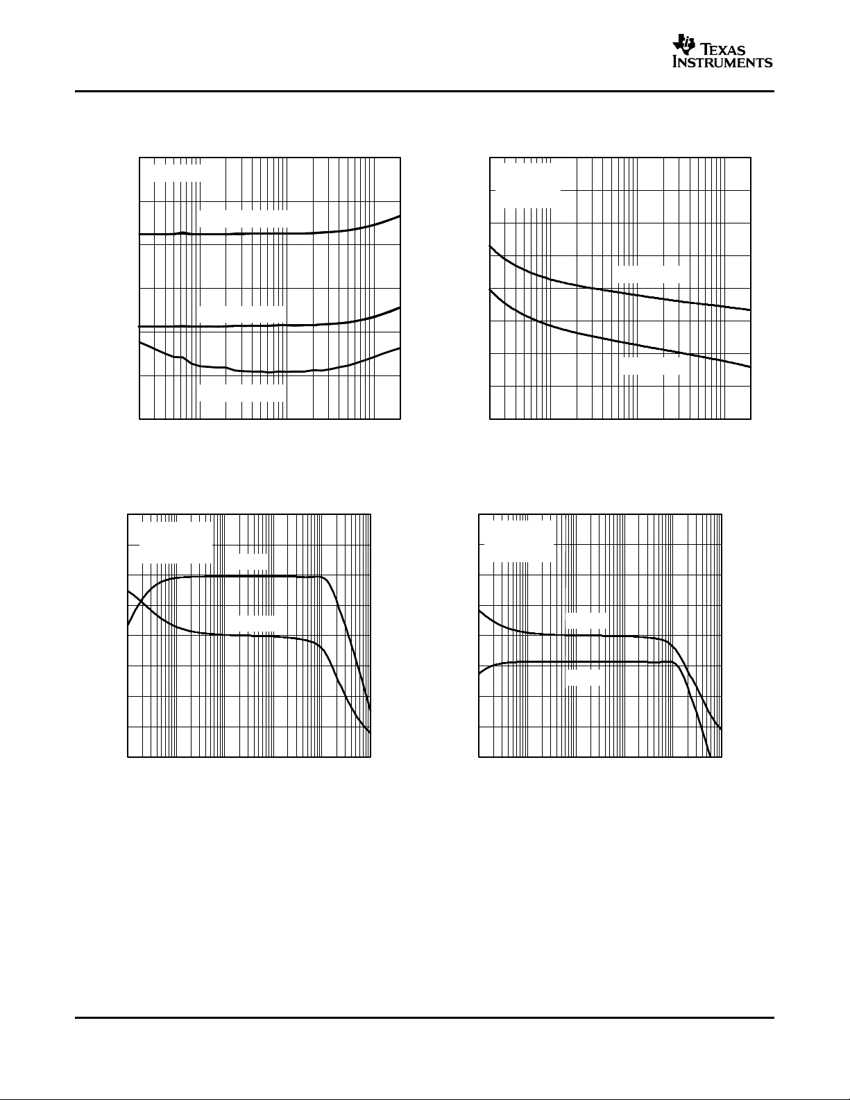
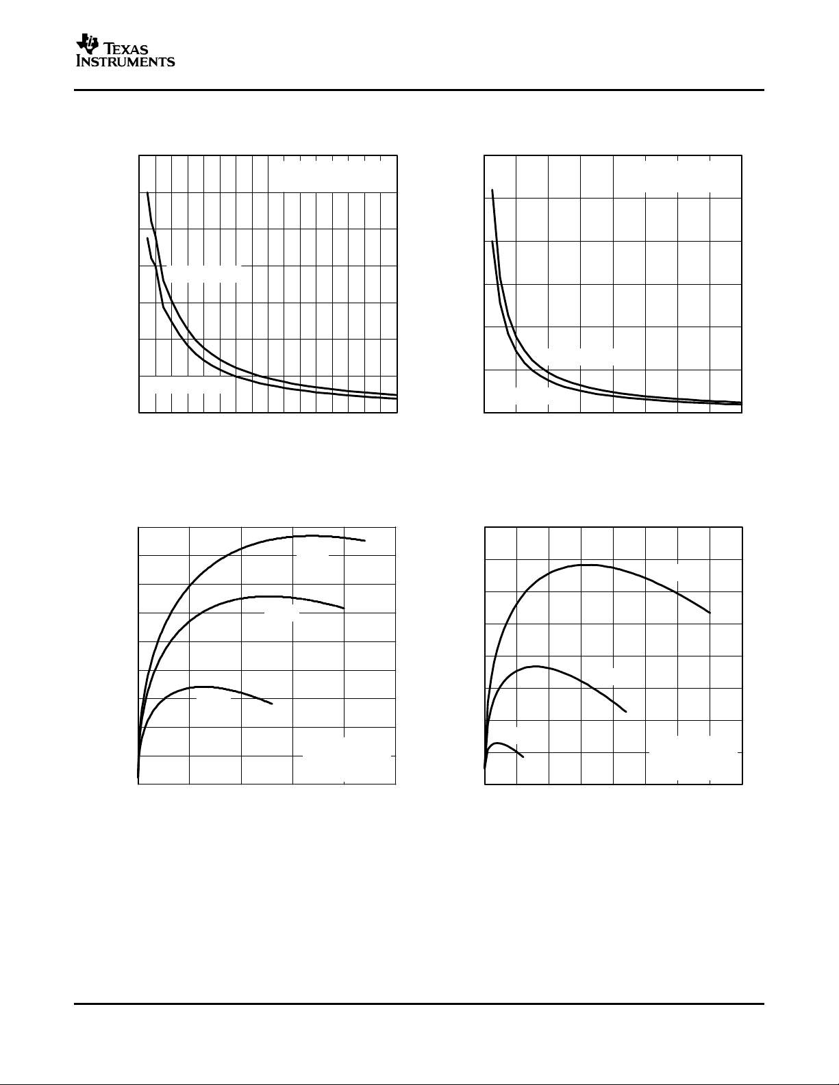
Table of Graphs
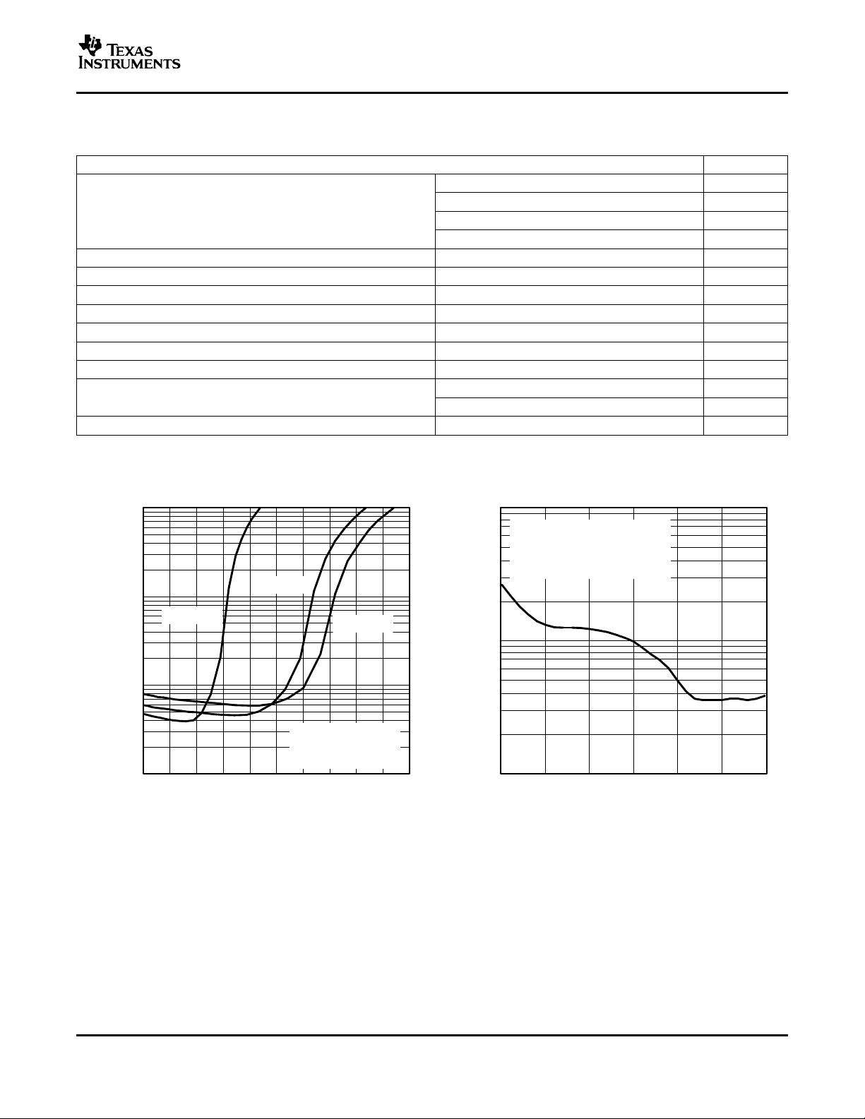
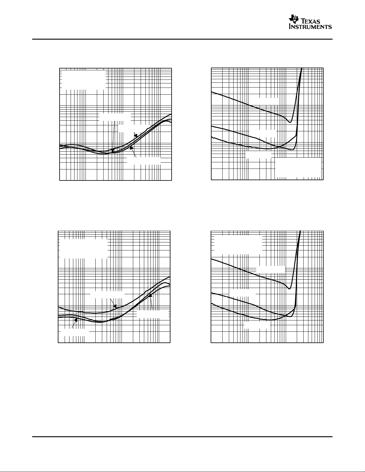
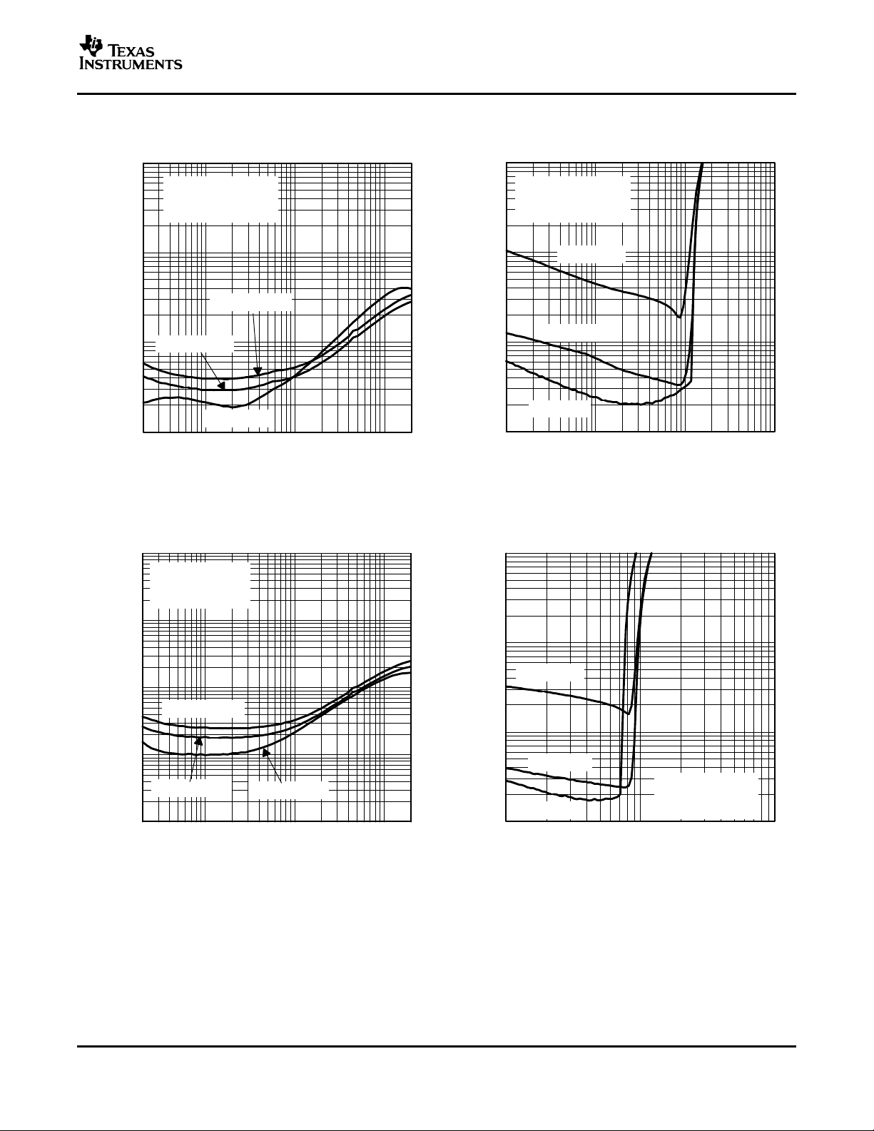
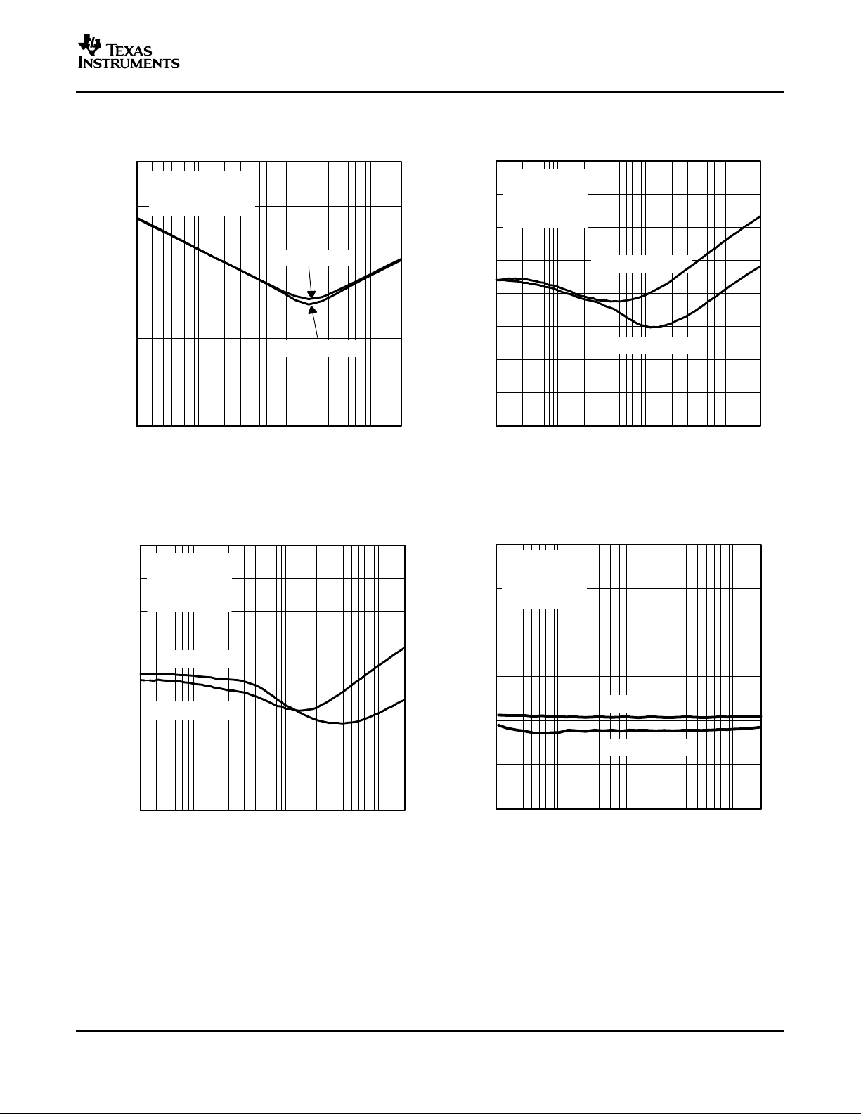
vs Output power 1, 4, 6, 8, 10
THD+N Total harmonic distortion plus noise
V
n
Output noise voltage vs Frequency 13
Supply ripple rejection ratio vs Frequency 14, 15
Crosstalk vs Frequency 16, 17, 18
Shutdown attenuation vs Frequency 19
SNR Signal-to-noise ratio vs Frequency 20
Closed loop response 21, 22
P
O
P
D
Z
i
Output power vs Load resistance 23, 24
Power dissipation
Input impedance vs Gain 28
vs Voltage gain 2
vs Frequency 3, 5, 7, 9, 11
vs Output voltage 12
vs Output power 25, 26
vs Ambient temperature 27
TPA0132
FIGURE
TOTAL HARMONIC DISTORTION PLUS NOISE TOTAL HARMONIC DISTORTION PLUS NOISE
vs vs
OUTPUT POWER VOLTAGE GAIN
Figure 1. Figure 2.
5
www.ti.com
0.1%
0.01%
0.01 0.1
1%
10%
1 10
f = 20 Hz
f = 1 kHz
PO - Output Power - W
RL = 3 Ω
AV = 20 to 0 dB
BTL
THD+N -Total Harmonic Distortion + Noise
f = 20 kHz
0.01%
10%
20 100 1k 10k 20k
THD+N -Total Harmonic Distortion + Noise
f - Frequency - Hz
1%
0.1%
RL = 3 Ω
AV = 20 to 0 dB
BTL
PO = 1.75 W
PO = 0.5 W
PO = 1 W
0.1%
0.01%
20 100
1%
10%
1k 10k
f - Frequency - Hz
RL = 4 Ω
AV = 20 to 0 dB
BTL
THD+N -Total Harmonic Distortion + Noise
P
O
= 0.25 W
20k
P
O
= 1 W
P
O
= 1.5 W
0.1%
0.01%
0.01 0.1
1%
10%
1 10
f = 20 Hz
f = 1 kHz
PO - Output Power - W
THD+N -Total Harmonic Distortion + Noise
f = 20 kHz
RL = 4 Ω
AV = 20 to 0 dB
BTL
TPA0132
SLOS223E – MAY 1999 – REVISED SEPTEMBER 2004
TOTAL HARMONIC DISTORTION PLUS NOISE TOTAL HARMOINIC DISTORTION PLUS NOISE
vs vs
FREQUENCY OUTPUT POWER
Figure 3. Figure 4.
TOTAL HARMONIC DISTORTION PLUS NOISE TOTAL HARMONIC DISTORTION PLUS NOISE
vs vs
FREQUENCY OUTPUT POWER
6
Figure 5. Figure 6.
www.ti.com
0.1%
0.01%
0.01 0.1
1%
10%
1 10
f = 20 Hz
f = 1 kHz
PO - Output Power - W
THD+N -Total Harmonic Distortion + Noise
f = 20 kHz
RL = 8 Ω
AV = 20 to 0 dB
BTL
0.01%
10%
20 100 1k 10k 20k
THD+N -Total Harmonic Distortion + Noise
f - Frequency - Hz
1%
0.1%
PO = 0.25 W
P
O
= 0.5 W
PO = 1 W
RL = 8 Ω
AV = 20 to 0 dB
BTL
0.1%
0.01%
20
1%
10%
10k
f - Frequency - Hz
THD+N -Total Harmonic Distortion + Noise
PO = 25 mW
20k
RL = 32 Ω
AV = 14 to 0 dB
SE
PO = 50 mW
PO = 75 mW
100 1k
0.001%
0.1%
0.01%
0.01 0.1
1%
10%
1
f = 20 Hz
f = 1 kHz
PO - Output Power - W
THD+N -Total Harmonic Distortion + Noise
f = 20 kHz
RL = 32 Ω
AV = 14 to 0 dB
SE
TPA0132
SLOS223E – MAY 1999 – REVISED SEPTEMBER 2004
TOTAL HARMONIC DISTORTION PLUS NOISE TOTAL HARMONIC DISTORTION PLUS NOISE
vs vs
FREQUENCY OUTPUT POWER
Figure 7. Figure 8.
TOTAL HARMONIC DISTORTION PLUS NOISE TOTAL HARMONIC DISTORTION PLUS NOISE
vs vs
FREQUENCY OUTPUT POWER
Figure 9. Figure 10.
7
www.ti.com
THD+N -Total Harmonic Distortion + Noise
f = 20 kHz
VO - Output Voltage - V
RMS
0 0.2 0.4 0.6 0.8 1 1.2 1.4 1.6 1.8 2
0.001%
0.01%
0.1%
1%
10%
RL = 10 kΩ
AV = 14 to 0 dB
SE
f = 1 kHz
f = 20 Hz
0.001%
10%
20 100 1k 10k 20k
THD+N -Total Harmonic Distortion + Noise
f - Frequency - Hz
1%
0.1%
VO = 1 V
RMS
0.01%
RL = 10 kΩ
AV = 14 to 0 dB
SE
120
0
20 100
140
160
1k 10k
BW − Bandwidth − Hz
VDD = 5 V
BW = 22 Hz to 22 kHz
RL = 4 Ω
AV = 20 dB
20k
AV = 6 dB
− Output Noise Voltage − VµV
n
RMS
20
40
60
80
100
-100
-120
20 100
-80
1k 10k
RL = 8 Ω
C
(BYP)
= 0.47 µF
BTL
Supply Ripple Rejection Ratio - dB
A
V
= 6 dB
-60
-40
-20
0
f - Frequency - Hz
20k
A
V
= 20 dB
TPA0132
SLOS223E – MAY 1999 – REVISED SEPTEMBER 2004
TOTAL HARMONIC DISTORTION PLUS NOISE TOTAL HARMONIC DISTORTION PLUS NOISE
vs vs
FREQUENCY OUTPUT VOLTAGE
Figure 11. Figure 12.
OUTPUT NOISE VOLTAGE SUPPLY RIPPLE REJECTION RATIO
vs vs
BANDWIDTH FREQUENCY
8
Figure 13. Figure 14.
www.ti.com
-100
-120
20 100
-80
1k 10k
RL = 32 Ω
C
(BYP)
= 0.47 µF
SE
A
V
= 6 dB
-60
-40
-20
0
f - Frequency - Hz
20k
A
V
= 14 dB
Supply Ripple Rejection Ratio - dB
-120
-80
20 100 1k 10k 20k
Crosstalk - dB
f - Frequency - Hz
-90
-100
-110
PO = 1 W
RL = 8 Ω
AV = 20 dB
BTL
-70
-60
Left to Right
Right to Left
-50
-40
-120
-40
20 100 1k 10k 20k
Crosstalk - dB
f - Frequency - Hz
-60
-80
-100
VO = 1 V
RMS
RL = 10 kΩ
AV = 6 dB
SE
-20
0
Left to Right
Right to Left
−120
−80
20 100 1k 10k 20k
Crosstalk − dB
f − Frequency − Hz
−90
−100
−110
PO = 1 W
RL = 8 Ω
AV = 6 dB
BTL
−70
−60
Left to Right
Right to Left
−50
−40
TPA0132
SLOS223E – MAY 1999 – REVISED SEPTEMBER 2004
SUPPLY RIPPLE REJECTION RATIO CROSSTALK
vs vs
FREQUENCY FREQUENCY
Figure 15. Figure 16.
CROSSTALK CROSSTALK
vs vs
FREQUENCY FREQUENCY
Figure 17. Figure 18.
9
www.ti.com
-120
-40
20 100 1k 10k 20k
Shutdown Attenuation - dB
f - Frequency - Hz
-60
-80
-100
-20
0
VI = 1 V
RMS
RL = 8 Ω, BTL
RL = 32 Ω, SE
RL = 10 kΩ, SE
80
110
20 100 1k 10k 20k
SNR − Signal-To-Noise Ratio − dB
f − Frequency − Hz
105
100
95
115
120
85
90
PO = 1 W
RL = 8 Ω
BTL
AV = 20 dB
AV = 6 dB
-10
20
10 100 1k 10k 100k
Gain - dB
f - Frequency - Hz
15
10
5
25
30
-5
0
180°
90°
0°
-90°
-180°
1M
Phase
RL = 8 Ω
AV = 20 dB
BTL
Gain
Phase
-10
20
10 100 1k 10k 100k
Gain - dB
f - Frequency - Hz
15
10
5
25
30
-5
0
180°
90°
0°
-90°
-180°
1M
RL = 8 Ω
AV = 6 dB
BTL
Gain
Phase
Phase
TPA0132
SLOS223E – MAY 1999 – REVISED SEPTEMBER 2004
SHUTDOWN ATTENUATION SIGNAL-TO-NOISE RATIO
vs vs
FREQUENCY FREQUENCY
Figure 19. Figure 20.
CLOSED LOOP RESPONSE CLOSED LOOP RESPONSE
10
Figure 21. Figure 22.
www.ti.com
2
1.5
0
0 8 16 24 32 40
2.5
3
3.5
48 56 64
RL - Load Resistance - Ω
AV = 20 to 0 dB
BTL
- Output Power - WP
O
1% THD+N
10% THD+N
1
0.5
750
0
0 8 16
1000
1250
1500
24 32
RL - Load Resistance - Ω
AV = 14 to 0 dB
SE
- Output Power - mWP
O
1% THD+N
10% THD+N
500
250
40 48 56 64
0.6
0.4
0.2
0
0 1
- Power Dissipation - W
1
1.2
1.4
1.5 2.5
0.8
PO - Output Power - W
P
D
4 Ω
8 Ω
f = 1 kHz
BTL
Each Channel
3 Ω
1.6
1.8
0.5 2
0.1
0.05
0
0 0.2
- Power Dissipation - W
0.2
0.25
0.3
0.3 0.8
0.15
PO - Output Power - W
P
D
8 Ω
32 Ω
f = 1 kHz
SE
Each Channel
4 Ω
0.35
0.4
0.1 0.70.4 0.5 0.6
SLOS223E – MAY 1999 – REVISED SEPTEMBER 2004
OUTPUT POWER OUTPUT POWER
vs vs
LOAD RESISTANCE LOAD RESISTANCE
TPA0132
Figure 23. Figure 24.
POWER DISSIPATION POWER DISSIPATION
vs vs
OUTPUT POWER OUTPUT POWER
Figure 25. Figure 26.
11
www.ti.com
40
30
20
10
−40 −20
60
70
80
−10 10
50
AV − Gain − dB
90
−30 0 20
− Input Impedance −Z
I
Ωk
1
0
-40 0
- Power Dissipation - W
3
4
5
20 160
2
TA - Ambient Temperature - °C
P
D
6
7
-20 10040 60 80 120 140
Θ
JA3
Θ
JA1,2
Θ
JA4
Θ
JA1
= 45.9°C/W
Θ
JA2
= 45.2°C/W
Θ
JA3
= 31.2°C/W
Θ
JA4
= 18.6°C/W
TPA0132
SLOS223E – MAY 1999 – REVISED SEPTEMBER 2004
POWER DISSIPATION INPUT IMPEDANCE
vs vs
AMBIENT TEMPERATURE GAIN
Figure 27. Figure 28.
12

www.ti.com
TPA0132
SLOS223E – MAY 1999 – REVISED SEPTEMBER 2004
Volume Control Characteristics
Table 1. Typical DC Volume Control
VOLUME (Terminal 3)
VOLTAGE INCREASING VOLTAGE
OR FIXED GAIN DECREASING
(V) (V)
0-0.27 0.16-0 20
0.28-0.37 0.28-0.17 18
0.38-0.48 0.39-0.29 16
0.49-0.58 0.50-0.40 14
0.59-0.69 0.61-0.51 12
0.70-0.80 0.72-0.62 10
0.81-0.91 0.84-0.73 8
0.92-1.02 0.95-0.85 6
1.03-1.13 1.06-0.96 4
1.14-1.24 1.17-1.07 2
1.25-1.35 1.29-1.18 0
1.36-1.46 1.40-1.30 -2
1.47-1.58 1.51-1.41 -4
1.59-1.68 1.62-1.52 -6
1.69-1.79 1.73-1.63 -8
1.80-1.90 1.84-1.74 -10
1.91-2.01 1.96-1.85 -12
2.02-2.12 2.06-1.97 -14
2.13-2.23 2.18-2.07 -16
2.24-2.34 2.29-2.19 -18
2.35-2.45 2.41-2.30 -20
2.46-2.56 2.52-2.42 -22
2.57-2.67 2.62-2.53 -24
2.68-2.78 2.74-2.63 -26
2.79-2.90 2.86-2.75 -28
2.91-3.01 2.97-2.87 -30
3.02-3.12 3.07-2.98 -32
3.13-3.23 3.19-3.08 -34
3.24-3.33 3.29-3.20 -36
3.34-3.44 3.40-3.30 -38
3.45-3.55 3.53-3.41 -40
3.56-5.00 5.00-3.54 -85
(1)
TYPICAL
GAIN of AMPLIFIER
(2)
(dB)
(1) Each step is tested at its midpoint and characterized within ± 4dB of the specified gain value for V
5 V. For V
(2) 95% of the characterized values lie within ± 0.5dB of the specified gain value. Figure 29 shows the
typical behavior of most devices.
= 4.5 V to 5.5 V, multiply values by 90% and 110%, respectively.
DD
=
DD
13

www.ti.com
0
10
20
30
40
50
60
70
80
90
100
Gain − dB
−4
−3
−2
−1
0
1
2
3
4
Frequency of Occurance − %
TPA0132
SLOS223E – MAY 1999 – REVISED SEPTEMBER 2004
GAIN HISTOGRAM AT 0 dB
Figure 29. Typical Gain Variance
14

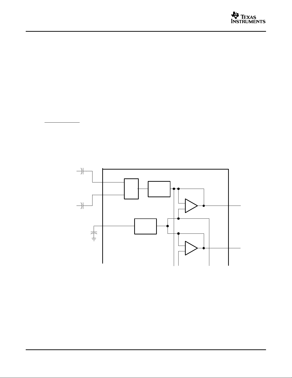
www.ti.com
ROUT+ 21
R
MUX
RHPIN
RLINEIN
+
-
23
20
C
IRHP
0.47 µF
Right
Headphone
Input
Signal
C
IRLINE
0.47 µF
Right
Line
Input
Signal
C
RIN
0.47 µF
8 RIN
ROUT- 16
+
-
1 kΩ
C
OUTR
330 µF
100 kΩ
L
MUX
LHPIN
LLINEIN5
6
C
ILHP
0.47 µF
Left
Headphone
Input
Signal
C
ILLINE
0.47 µF
Left
Line
Input
Signal
C
LIN
0.47 µF
10 LIN
1 kΩ
C
OUTL
330 µF
V
DD
100 kΩ
Depop
Circuitry
Power
Management
PV
DD
18
V
DD
19
BYPASS 11
SHUT-
DOWN
22
GND
LOUT+ 4
+
-
LOUT- 9
+
-
C
BYP
0.47 µF
1, 12,
13, 24
To
System
Control
C
SR
0.1 µF
V
DD
C
SR
0.1 µF
V
DD
See Note A
PC-
Beep
PC-BEEP
14
C
PCB
0.47 µF
PC-BEEP
Input
Signal
Gain/
MUX
Control
VOLUME
CLK
3
17
SE/BTL
15
C
CLK
47 nF
V
DD
50 kΩ
32-Step
Volume
Control
32-Step
Volume
Control
32-Step
Volume
Control
32-Step
Volume
Control
SLOS223E – MAY 1999 – REVISED SEPTEMBER 2004
APPLICATION INFORMATION
COMPONENT SELECTION
Figure 30 and Figure 31 are schematic diagrams of typical notebook computer application circuits.
TPA0132
NOTE: A 0.1-µF ceramic capacitor should be placed as close as possible to the IC. For filtering lower-frequency noise
signals, a larger electrolytic capacitor of 10 µF or greater should be placed near the audio power amplifier.
Figure 30. Typical TPA0132 Application Circuit Using Single-Ended Inputs and Input MUX
15

www.ti.com
23
C
CLK
47 nF
SE/BTL
ROUT+ 21
R
MUX
RHPIN
RLINEIN
+
−
20
C
IRIN−
0.47 µF
8 RIN
ROUT− 16
+
−
1 kΩ
C
OUTR
330 µF
100 kΩ
L
MUX
LHPIN
LLINEIN5
6
C
ILIN−
0.47 µF
10 LIN
1 kΩ
C
OUTL
330 µF
V
DD
100 kΩ
Depop
Circuitry
Power
Management
PV
DD
18
V
DD
19
BYPASS 11
SHUT−
DOWN
22
GND
LOUT+
4
+
−
LOUT−
9
+
−
C
BYP
0.47 µF
1, 12,
13, 24
To
System
Control
C
SR
0.1 µF
V
DD
C
SR
0.1 µF
V
DD
See Note A
PC-
Beep
PC-BEEP14
C
PCB
0.47 µF
PC-BEEP
Input
Signal
Gain/
MUX
Control
VOLUME
CLK
3
1717
C
IRIN+
0.47 µF
V
DD
50 kΩ
15
C
ILIN
0.47 µF
32-Step
Volume
Control
32-Step
Volume
Control
32-Step
Volume
Control
C
IRHP−
0.47 µF
32-Step
Volume
Control
2
PCB
ENABLE
C
ILHP
0.47 µF
Right
Positive
Differential
Input Signal
Right
Negative
Differential
Input Signal
Left
Negative
Differential
Input Signal
Left
Positive
Differential
Input Signal
TPA0132
SLOS223E – MAY 1999 – REVISED SEPTEMBER 2004
APPLICATION INFORMATION (continued)
Figure 31. Typical TPA0132 Application Circuit Using Differential Inputs
NOTE: A 0.1-µF ceramic capacitor should be placed as close as possible to the IC. For filtering lower-frequency noise
signals, a larger electrolytic capacitor of 10 µF or greater should be placed near the audio power amplifier.
16

www.ti.com
Decreasing Voltage on
VOLUME Terminal
Increasing Voltage on
VOLUME Terminal
1.17 1.36
1.25 1.29
-2
0
2
Gain - dB
Voltage on VOLUME Pin - V
C
R
IN
R
i
R
f
TPA0132
SLOS223E – MAY 1999 – REVISED SEPTEMBER 2004
APPLICATION INFORMATION (continued)
VOLUME CONTROL OPERATION
The VOLUME pin controls the volume of the TPA0132. It is controlled with a dc voltage, which should not exceed
V
. The gain voltages on the VOLUME pin are given in the Typical Characteristics section.
DD
The trip point, where the gain actually changes, is different depending on whether the voltage on the VOLUME
terminal is increasing or decreasing as a result of hysteresis about each trip point. The hysteresis ensures that
the gain control is monotonic and does not oscillate from one gain step to another. A pictorial representation of
the volume control can be found in Figure 32 . The graph focuses on three gain steps with the trip points defined
in the first and second columns of the Typical DC Volume Control table. The dotted lines represent the hysteresis
about each gain step.
DC Volume Control Operation
Figure 32.
INPUT RESISTANCE
The gain is set by varying the input resistance of the amplifier, which can range from its smallest value to over
six times that value. As a result, if a single capacitor is used in the input high pass filter, the –3 dB or cut-off
frequency also changes by over six times. Connecting an additional resistor from the input pin of the amplifier to
ground, as shown in Figure 33 , reduces the cutoff-frequency variation.
Figure 33. Resistor on Input for Cut-Off Frequency
The input resistance at each gain setting is given in the graph for Input Impedance vs Gain in the Typical
Characteristics section.
The –3-dB frequency can be calculated using Equation 1 .
17

www.ti.com
ƒ
–3 dB
1
2 CR R
i
f
c(highpass)
1
2 ZINC
i
−3 dB
f
c
C
i
1
2 Z
i
f
c
TPA0132
SLOS223E – MAY 1999 – REVISED SEPTEMBER 2004
APPLICATION INFORMATION (continued)
To increase filter accuracy, increase the value of the capacitor and decrease the value of the resistor to ground.
In addition, the order of the filter can be increased.
(1)
INPUT CAPACITOR, C
In a typical application, an input capacitor (C
proper dc level for optimum operation. In this case, C
i
) is required to allow the amplifier to bias the input signal to the
i
and the input impedance of the amplifier (Z
i
) form a
i
high-pass filter with the corner frequency determined by Equation 2 .
The value of Cidirectly affects the bass (low frequency) performance of the circuit. Consider the example where
Ziis 55 k Ω and the specification calls for a flat bass response down to 30 Hz. Equation 2 is reconfigured as
Equation 3 .
In this example, C
consideration for this capacitor is the leakage path from the input source through the input network (C
is 72 nF, so one would likely choose a value in the range of 0.1 µF to 1 µF. A further
i
) and the
i
feedback network to the load. This leakage current creates a dc offset voltage at the input to the amplifier that
reduces useful headroom, especially in high-gain applications. For this reason a low-leakage tantalum or ceramic
capacitor is the best choice. When polarized capacitors are used, connect the positive lead of the capacitor to
the amplifier input in most applications, as the dc level there is held at V
/2, typically higher than the source dc
DD
level. Note that it is important to confirm the capacitor polarity in the application.
(2)
(3)
POWER SUPPLY DECOUPLING, C
(S)
This high-performance CMOS audio amplifier requires adequate power-supply decoupling to minimize output
total harmonic distortion (THD). Power-supply decoupling also prevents oscillations with long lead lengths
between the amplifier and the speaker. Optimum decoupling is achieved by using two capacitors of different
types that target different types of noise on the power-supply leads. To filter high-frequency transients, spikes, or
digital hash on the line, a good low equivalent-series-resistance (ESR) ceramic capacitor, typically 0.1 µF, placed
as close as possible to the device V
lead, works best. For filtering low-frequency noise signals, an aluminum
DD
electrolytic capacitor of 10 µF or greater placed near the audio power amplifier is recommended.
MIDRAIL BYPASS CAPACITOR, C
The midrail bypass capacitor, C
startup or recovery from shutdown mode, C
(BYP)
(BYP)
, is the most critical capacitor and serves several important functions. During
determines the rate at which the amplifier starts up. The second
(BYP)
function is to reduce power-supply noise coupling into the output drive signal. This noise is from the midrail
generation circuit internal to the amplifier, and appears as degraded PSRR and THD+N.
Bypass capacitor (C
recommended for best THD and noise performance.
18
) values of 0.47-µF to 1-µF, and ceramic or tantalum low-ESR capacitors are
(BYP)

www.ti.com
f
c(high)
1
2 RLC
(C)
−3 dB
f
c
TPA0132
SLOS223E – MAY 1999 – REVISED SEPTEMBER 2004
APPLICATION INFORMATION (continued)
OUTPUT COUPLING CAPACITOR, C
In a typical single-supply SE configuration, an output coupling capacitor (C
the output of the amplifier to prevent dc currents in the load. As with the input coupling capacitor, the output
coupling capacitor and impedance of the load form a high-pass filter governed by Equation 4 .
The main disadvantage, from a performance standpoint, is that load impedances are typically small, driving the
low-frequency corner higher, degrading the bass response. Large values of C
frequencies into the load. Consider the example where a C
Ω , 32 Ω , 10 k Ω , and 47 k Ω . Table 2 summarizes the frequency response characteristics of each configuration.
(C)
) is required to block the dc bias at
(C)
are required to pass low
of 330 µF is chosen and loads include 3 Ω , 4 Ω , 8
(C)
(C)
(4)
Table 2. Common Load Impedances Vs Low Frequency
Output Characteristics in SE Mode
R
L
3 Ω 330 µF 161 Hz
4 Ω 330 µF 120 Hz
8 Ω 330 µF 60 Hz
32 Ω 330 µF 15 Hz
10,000 Ω 330 µF 0.05 Hz
47,000 Ω 330 µF 0.01 Hz
C
(C)
LOWEST FREQUENCY
As Table 2 indicates, most of the bass response is attenuated into a 4- Ω load, an 8- Ω load is adequate,
headphone response is good, and drive into line level inputs (a home stereo for example) is exceptional.
USING LOW-ESR CAPACITORS
Low-ESR capacitors are recommended throughout this applications section. A real (as opposed to ideal)
capacitor can be modeled simply as a resistor in series with an ideal capacitor. The voltage drop across this
resistor minimizes the beneficial effects of the capacitor in the circuit. The lower the equivalent value of this
resistance the more the real capacitor behaves like an ideal capacitor.
19

www.ti.com
Power
V
(rms)
2
R
L
V
(rms)
V
O(PP)
2 2
R
L
2x V
O(PP)
V
O(PP)
−V
O(PP)
V
DD
V
DD
f
(c)
1
2 R
LC(C)
TPA0132
SLOS223E – MAY 1999 – REVISED SEPTEMBER 2004
BRIDGED-TIED LOAD VS SINGLE-ENDED MODE
Figure 34 shows a Class-AB audio power amplifier (APA) in a BTL configuration. The TPA0132 amplifier consists
of two Class-AB amplifiers driving both ends of the load. There are several potential benefits to this differential
drive configuration, but, initially consider power to the load. The differential drive to the speaker means that as
one side is slewing up, the other side is slewing down, and vice versa. This in effect doubles the voltage swing
on the load as compared to a ground referenced load. Substituting 2 × V
voltage is squared, yields 4 × the output power from the same supply rail and load impedance (see Equation 5 ).
into the power equation, where
O(PP)
(5)
Figure 34. Bridge-Tied Load Configuration
In a typical computer sound channel operating at 5 V, bridging raises the power into an 8- Ω speaker from a
singled-ended (SE, ground reference) limit of 250 mW to 1 W. In sound power, this is a 6-dB improvement —
loudness that can be heard. In addition to increased power there are frequency-response concerns. Consider the
single-supply SE configuration shown in Figure 35 . A coupling capacitor is required to block the dc offset voltage
from reaching the load. These capacitors can be quite large (approximately 33 µF to 1000 µF), so they tend to be
expensive, heavy, occupy valuable PCB area, and have the additional drawback of limiting the low-frequency
performance of the system. This frequency-limiting effect is due to the high-pass filter network created with the
speaker impedance and the coupling capacitance, and is calculated with Equation 6 .
For example, a 68-µF capacitor with an 8- Ω speaker would attenuate low frequencies below 293 Hz. The BTL
configuration cancels the dc offsets, eliminating the need for blocking capacitors. Low-frequency performance is
then limited only by the input network and speaker response. Cost and PCB space are also minimized by
eliminating the bulky coupling capacitor.
20
(6)

www.ti.com
R
L
C
(C)
V
O(PP)
V
O(PP)
V
DD
−3 dB
f
c
V
(LRMS)
V
O
I
DD
I
DD(avg)
TPA0132
SLOS223E – MAY 1999 – REVISED SEPTEMBER 2004
Figure 35. Single-Ended Configuration and Frequency Response
Increasing power to the load does carry a penalty of increased internal power dissipation. The increased
dissipation is understandable, since the BTL configuration produces 4 × the output power of the SE configuration.
Internal dissipation versus output power is discussed further in the Crest Factor and Thermal Considerations
section.
Single-Ended Operation
In SE mode (see Figure 35 ), the load is driven from the primary amplifier output for each channel (LOUT+ and
ROUT+).
The amplifier switches to single-ended operation when the SE/ BTL terminal is held high. This puts the negative
outputs in a high-impedance state, and reduces the amplifier's gain by 6 dB.
BTL AMPLIFIER EFFICIENCY
Class-AB amplifiers are inefficient, primarily because of voltage drop across the output-stage transistors. The two
components of the internal voltage drop are the headroom or dc voltage drop that varies inversely to output
power, and the sine wave nature of the output. The total voltage drop can be calculated by subtracting the RMS
value of the output voltage from V
(I
rms) determines the internal power dissipation of the amplifier.
DD
An easy-to-use equation to calculate efficiency begins as the ratio of power from the power supply to the power
delivered to the load. To accurately calculate the RMS and average values of power in the load and in the
amplifier, the current and voltage waveforms must be understood (see Figure 36 ).
Figure 36. Voltage and Current Waveforms for BTL Amplifiers
Although the voltages and currents for SE and BTL are sinusoidal in the load, currents from the supply are very
different between SE and BTL configurations. In an SE application, the current waveform is a half-wave rectified
shape, whereas in BTL it is a full-wave rectified waveform. Therefore, RMS conversion factors are different. Keep
in mind that for most of the waveform both the push and pull transistors are not on at the same time, which
supports the fact that each amplifier in the BTL device only draws current from the supply for half the waveform.
Equation 7 and Equation 8 are the basis for calculating amplifier efficiency.
. The internal voltage drop multiplied by the RMS value of the supply current
DD
21

www.ti.com
Efficiency of a BTL amplifier
P
L
P
SUP
Where:
P
L
VLrms
2
R
L
, andV
LRMS
V
P
2
, therefore, P
L
V
P
2
2R
L
and
P
SUP
VDDIDDavg
and
IDDavg
1
0
V
P
R
L
sin(t) dt
1
V
P
R
L
[cos(t)]
0
2V
P
R
L
Therefore,
P
SUP
2 VDDV
P
R
L
substituting PL and P
SUP
into equation 7,
Efficiency of a BTL a mplifier
V
P
2
2 R
L
2 VDDV
P
R
L
V
P
4 V
DD
VP 2 PLR
L
Where:
PL = Power delivered to load
P
SUP
= Power drawn from power supply
V
LRMS
= RMS voltage on BTL load
R
L
= Load resistance
BTL
2 PLR
L
4 V
DD
Therefore,
VP = Peak voltage on BTL load
IDDavg = Average current drawn from the power supply
VDD = Power supply voltage
η
BTL
= Efficiency of a BTL amplifier
TPA0132
SLOS223E – MAY 1999 – REVISED SEPTEMBER 2004
Table 3 employs Equation 8 to calculate efficiencies for four different output-power levels. Note that the efficiency
of the amplifier is quite low for lower power levels and rises sharply as power to the load is increased resulting in
a nearly flat internal power dissipation over the normal operating range. Note that the internal dissipation at full
output power is less than in the half-power range. Calculating the efficiency for a specific system is the key to
proper power supply design. For a stereo 1-W audio system with 8- Ω loads and a 5-V supply, the maximum draw
on the power supply is almost 3.25 W.
22
Table 3. Efficiency vs Output Power in 5-V, 8- Ω BTL Systems
OUTPUT POWER (W) PEAK VOLTAGE (V) INTERNAL DISSIPATION (W)
0.25 31.4 2.00 0.55
(1) High peak voltages cause the THD to increase.
0.50 44.4 2.83 0.62
1.00 62.8 4.00 0.59
1.25 70.2 4.47
EFFICIENCY
(%)
(1)
0.53
(7)
(8)

www.ti.com
PdB 10Log
P
W
P
ref
10Log
4 W
1 W
6 dB
TPA0132
SLOS223E – MAY 1999 – REVISED SEPTEMBER 2004
CREST FACTOR AND THERMAL CONSIDERATIONS
Class-AB power amplifiers dissipate a significant amount of heat in the package under normal operating
conditions. A typical music CD requires 12 dB to 15 dB of dynamic range, or headroom, above the average
power output, to pass the loudest portions of the signal without distortion. In other words, music typically has a
crest factor between 12 dB and 15 dB. When determining the optimal ambient operating temperature, the internal
dissipated power at the average output power level must be used. From the data sheet, one can see that when
the device is operating from a 5-V supply into a 3- Ω speaker that 4-W peaks are available. Use Equation 9 to
convert watts to dB.
Subtracting the headroom restriction to obtain the average listening level without distortion yields:
6 dB - 15 dB = -9 dB (15-dB crest factor)
6 dB - 12 dB = -6 dB (12-dB crest factor)
6 dB - 9 dB = -3 dB (9-dB crest factor)
6 dB - 6 dB = 0 dB (6-dB crest factor)
6 dB - 3 dB = 3 dB (3-dB crest factor)
(9)
Converting dB back into watts:
P
W
PdB/10
= 10
× P
ref
= 63 mW (18-dB crest factor)
= 125 mW (15-dB crest factor)
= 250 mW (9-dB crest factor)
= 500 mW (6-dB crest factor)
= 1000 mW (3-dB crest factor)
= 2000 mW (0-dB crest factor)
This is valuable information to consider when estimating the heat-dissipation requirements for the amplifier
system. Comparing the worst case, 2 W of continuous power output with a 3-dB crest factor, against 12-dB and
15-dB applications, drastically affects maximum ambient temperature ratings for the system. Using the power
dissipation curves for a 5-V, 3- Ω system, the internal dissipation and maximum ambient temperatures are shown
in the table below.
Table 4. TPA0132 Power Rating, 5-V, 3- Ω Stereo
PEAK OUTPUT POWER POWER DISSIPATION MAXIMUM AMBIENT
(W) (W/Channel) TEMPERATURE
4 2 W (3 dB) 1.7 -3 ° C
4 1000 mW (6 dB) 1.6 6 ° C
4 500 mW (9 dB) 1.3 24 ° C
4 250 mW (12 dB) 1.0 51 ° C
4 125 mW (15 dB) 0.9 78 ° C
4 63 mW (18 dB) 0.6 85 ° C
(1) Package limited to 85 ° C ambient
AVERAGE OUTPUT POWER
(1)
23

www.ti.com
Dmax
2V
2
DD
2
R
L
θ
JA
1
Derating Factor
1
0.022
45°CW
TAMax TJMax θJAP
D
150 45(0.6 2) 96°C(15-dB crest factor
)
TPA0132
SLOS223E – MAY 1999 – REVISED SEPTEMBER 2004
Table 5. TPA0132 Power Rating, 5-V, 8- Ω Stereo
PEAK OUTPUT POWER POWER DISSIPATION MAXIMUM AMBIENT
(W) (W/Channel) TEMPERATURE
2.5 1250 mW (3-dB crest factor) 0.53 85 ° C
2.5 1000 mW (4-dB crest factor) 0.59 85 ° C
2.5 500 mW (7-dB crest factor) 0.62 85 ° C
2.5 250 mW (10-dB crest factor) 0.55 85 ° C
(1) Package limited to 85 ° C ambient
AVERAGE OUTPUT POWER
(1)
(1)
(1)
(1)
(1)
The maximum dissipated power (P
8- Ω load. As a result, the formula in Equation 10 for calculating P
However, in the case of an 8- Ω load, the P
The amplifier may therefore be operated at a higher ambient temperature than required by the P
) is reached at a much lower output power level for a 3- Ω load than for an
Dmax
occurs at a point well above the normal operating power level.
Dmax
may be used for a 3- Ω application:
Dmax
Dmax
formula for
an 8- Ω load, but do not exceed the maximum ambient temperature of 85 ° .
The maximum ambient temperature depends on the heatsinking ability of the PCB system. The derating factor
for the PWP package is shown in the dissipation rating table. Converting this to θJA:
To calculate maximum ambient temperatures, first consider that the numbers from the dissipation graphs are
per-channel, so the dissipated heat is doubled for two-channel operation. Given θJA, the maximum allowable
junction temperature, and the total internal dissipation, the maximum ambient temperature can be calculated
using Equation 12 . The maximum recommended junction temperature for the device is 150 ° C. The internal
dissipation figures are taken from the Power Dissipation vs Output Power graphs.
NOTE:
Internal dissipation of 0.6 W is estimated for a 2-W system with 15-dB crest factor per
channel.
Due to package limitiations, the actual T
is 85 ° C.
AMAX
The power rating tables show that for some applications, no airflow is required to keep junction temperatures in
the specified range. The internal thermal protection turns the device off at junction temperatures higher than
150 ° C to prevent damage to the IC. The power rating tables in this section were calculated for maximum
listening volume without distortion. When the output level is reduced the numbers in the table change
significantly. Also, using 8- Ω speakers dramatically increases the thermal performance by increasing amplifier
efficiency.
(10)
(11)
(12)
24

www.ti.com
ROUT+ 21
R
MUX
RHPIN
RLINEIN
+
−
23
20
8 RIN
ROUT− 16
+
−
1 kΩ
C
OUTR
330 µF
100 kΩ
SE/BTL 15
100 kΩ
V
DD
32-Step
Volume
Control
32-Step
Volume
Control
TPA0132
SLOS223E – MAY 1999 – REVISED SEPTEMBER 2004
SE/ BTL OPERATION
The ability of the TPA0132 to easily switch between BTL and SE modes is one of its most important cost-saving
features. This feature eliminates the requirement for an additional headphone amplifier in applications where
internal stereo speakers are driven in BTL mode but external headphone or speakers must be accommodated.
Two separate internal amplifiers drive OUT+ and OUT–. The SE/ BTL input controls the operation of the follower
amplifier that drives LOUT– and ROUT–. When SE/ BTL is held low, the amplifier is on and the device is in the
BTL mode. When SE/ BTL is held high, the OUT– amplifiers are in a high output-impedance state, which
configures the device outputs as SE drivers from LOUT+ and ROUT+. IDDis reduced by approximately one-half
in SE mode. Control of the SE/ BTL input can be from a logic-level CMOS source or, more typically, from a
resistor-divider network as shown in Figure 37 .
Figure 37. TPA0132 Resistor Divider Network Circuit
Using a readily-available 1/8-in. (3,5 mm) stereo headphone jack, the control switch is closed when no plug is
inserted. When closed, the 100-k Ω /1-k Ω divider pulls the SE/ BTL input low. When a plug is inserted, the 1-k Ω
resistor is disconnected and the SE/ BTL input is pulled high. When the input goes high, the OUT– amplifier is
shut down, muting the speaker (virtually open-circuits the speaker). The OUT+ amplifier then drives through the
output capacitor (C
) into the headphone jack.
O
25
www.ti.com
C
PCB
1
2 ƒ
PCB
(100 k)
ROUT+ 21
R
MUX
RHPIN
RLINEIN
+
−
23
20
8 RIN
ROUT− 16
+
−
32-Step
Volume
Control
32-Step
Volume
Control
C
IRHP
0.47 µF
C
IRLINE
0.47 µF
Right
Headphone
Right Line
Input Signal
C
RIN
0.47 µF
TPA0132
SLOS223E – MAY 1999 – REVISED SEPTEMBER 2004
PC-BEEP OPERATION
The PC-BEEP input allows a system beep to be sent directly from a computer through the amplifier to the
speakers with few external components. The input is activated automatically. When the PC-BEEP input is active,
both LINEIN and HPIN inputs are deselected, and both the left and right channels are driven in BTL mode with
the signal from PC-BEEP. The gain from the PC-BEEP input to the speakers is fixed at 0.3 V/V and is
independent of the volume setting. When the PC-BEEP input is deselected, the amplifier returns to the previous
operating mode and volume setting. Furthermore, if the amplifier is in shutdown mode, activating PC-BEEP takes
the device out of shutdown, outputs the PC-BEEP signal, then returns the amplifier to shutdown mode.
When PCB ENABLE is held low, the amplifier automatically switches to PC-BEEP mode after detecting a valid
signal at the PC-BEEP input. The preferred input signal is a square wave or pulse train. To be accurately
detected, the signal must have a minimum of 1.5-V
minimum of eight rising edges. When the signal is no longer detected, the amplifier returns to its previous
operating mode and volume setting.
To ac-couple the PC-BEEP input, choose a coupling-capacitor value to satisfy Equation 13 .
The PC-BEEP input can also be dc-coupled to avoid using this coupling capacitor. The pin normally rests at
midrail when no signal is present.
INPUT MUX OPERATION
amplitude, rise and fall times of less than 0.1 µs and a
pp
(13)
Figure 38. TPA0132 Example Input MUX Circuit
The input MUX provides the user with a means to select from two different audio sources. In BTL mode, the
LINE inputs are selected. In SE mode, the HP inputs are selected. R
26
and L
IN
must be grounded in SE mode.
IN

PACKAGE OPTION ADDENDUM
www.ti.com
18-Apr-2006
PACKAGING INFORMATION
Orderable Device Status
(1)
Package
Type
Package
Drawing
Pins Package
Qty
Eco Plan
TPA0132PWP ACTIVE HTSSOP PWP 24 60 Green (RoHS &
no Sb/Br)
TPA0132PWPR ACTIVE HTSSOP PWP 24 2000 Green (RoHS &
no Sb/Br)
TPA0132PWPRG4 ACTIVE HTSSOP PWP 24 2000 Green (RoHS &
no Sb/Br)
(1)
The marketing status values are defined as follows:
ACTIVE: Product device recommended for new designs.
LIFEBUY: TI has announced that the device will be discontinued, and a lifetime-buy period is in effect.
NRND: Not recommended for new designs. Device is in production to support existing customers, but TI does not recommend using this part in
a new design.
PREVIEW: Device has been announced but is not in production. Samples may or may not be available.
OBSOLETE: TI has discontinued the production of the device.
(2)
Eco Plan - The planned eco-friendly classification: Pb-Free (RoHS), Pb-Free (RoHS Exempt), or Green (RoHS & no Sb/Br) - please check
http://www.ti.com/productcontent for the latest availability information and additional product content details.
TBD: The Pb-Free/Green conversion plan has not been defined.
Pb-Free (RoHS): TI's terms "Lead-Free" or "Pb-Free" mean semiconductor products that are compatible with the current RoHS requirements
for all 6 substances, including the requirement that lead not exceed 0.1% by weight in homogeneous materials. Where designed to be soldered
at high temperatures, TI Pb-Free products are suitable for use in specified lead-free processes.
Pb-Free (RoHS Exempt): This component has a RoHS exemption for either 1) lead-based flip-chip solder bumps used between the die and
package, or 2) lead-based die adhesive used between the die and leadframe. The component is otherwise considered Pb-Free (RoHS
compatible) as defined above.
Green (RoHS & no Sb/Br): TI defines "Green" to mean Pb-Free (RoHS compatible), and free of Bromine (Br) and Antimony (Sb) based flame
retardants (Br or Sb do not exceed 0.1% by weight in homogeneous material)
(2)
Lead/Ball Finish MSL Peak Temp
CU NIPDAU Level-2-260C-1 YEAR
CU NIPDAU Level-2-260C-1 YEAR
CU NIPDAU Level-2-260C-1 YEAR
(3)
(3)
MSL, Peak Temp. -- The Moisture Sensitivity Level rating according to the JEDEC industry standard classifications, and peak solder
temperature.
Important Information and Disclaimer:The information provided on this page represents TI's knowledge and belief as of the date that it is
provided. TI bases its knowledge and belief on information provided by third parties, and makes no representation or warranty as to the
accuracy of such information. Efforts are underway to better integrate information from third parties. TI has taken and continues to take
reasonable steps to provide representative and accurate information but may not have conducted destructive testing or chemical analysis on
incoming materials and chemicals. TI and TI suppliers consider certain information to be proprietary, and thus CAS numbers and other limited
information may not be available for release.
In no event shall TI's liability arising out of such information exceed the total purchase price of the TI part(s) at issue in this document sold by TI
to Customer on an annual basis.
Addendum-Page 1

IMPORTANT NOTICE
Texas Instruments Incorporated and its subsidiaries (TI) reserve the right to make corrections, modifications,
enhancements, improvements, and other changes to its products and services at any time and to discontinue
any product or service without notice. Customers should obtain the latest relevant information before placing
orders and should verify that such information is current and complete. All products are sold subject to TI’s terms
and conditions of sale supplied at the time of order acknowledgment.
TI warrants performance of its hardware products to the specifications applicable at the time of sale in
accordance with TI’s standard warranty. Testing and other quality control techniques are used to the extent TI
deems necessary to support this warranty . Except where mandated by government requirements, testing of all
parameters of each product is not necessarily performed.
TI assumes no liability for applications assistance or customer product design. Customers are responsible for
their products and applications using TI components. To minimize the risks associated with customer products
and applications, customers should provide adequate design and operating safeguards.
TI does not warrant or represent that any license, either express or implied, is granted under any TI patent right,
copyright, mask work right, or other TI intellectual property right relating to any combination, machine, or process
in which TI products or services are used. Information published by TI regarding third-party products or services
does not constitute a license from TI to use such products or services or a warranty or endorsement thereof.
Use of such information may require a license from a third party under the patents or other intellectual property
of the third party, or a license from TI under the patents or other intellectual property of TI.
Reproduction of information in TI data books or data sheets is permissible only if reproduction is without
alteration and is accompanied by all associated warranties, conditions, limitations, and notices. Reproduction
of this information with alteration is an unfair and deceptive business practice. TI is not responsible or liable for
such altered documentation.
Resale of TI products or services with statements different from or beyond the parameters stated by TI for that
product or service voids all express and any implied warranties for the associated TI product or service and
is an unfair and deceptive business practice. TI is not responsible or liable for any such statements.
Following are URLs where you can obtain information on other Texas Instruments products and application
solutions:
Products Applications
Amplifiers amplifier.ti.com Audio www.ti.com/audio
Data Converters dataconverter.ti.com Automotive www.ti.com/automotive
DSP dsp.ti.com Broadband www.ti.com/broadband
Interface interface.ti.com Digital Control www.ti.com/digitalcontrol
Logic logic.ti.com Military www.ti.com/military
Power Mgmt power.ti.com Optical Networking www.ti.com/opticalnetwork
Microcontrollers microcontroller.ti.com Security www.ti.com/security
Low Power Wireless www.ti.com/lpw Telephony www.ti.com/telephony
Video & Imaging www.ti.com/video
Wireless www.ti.com/wireless
Mailing Address: Texas Instruments
Post Office Box 655303 Dallas, Texas 75265
Copyright 2006, Texas Instruments Incorporated
 Loading...