
Please be aware that an important notice concerning availability, standard warranty, and use in critical applications of
Texas Instruments semiconductor products and disclaimers thereto appears at the end of this data sheet.
TP A0103
1.75-W 3-CHANNEL STEREO AUDIO POWER AMPLIFIER
SLOS167A – JULY 1997 – REVISED MARCH 2000
1
POST OFFICE BOX 655303 • DALLAS, TEXAS 75265
D
Desktop Computer Amplifier Solution
– 1.75-W Bridge Tied Load (BTL) Center
Channel
– 500-mW L/R Single-Ended Channels
D
Low Distortion Output
– < 0.05% THD+N at Full Power
D
Full 3.3-V and 5-V Specifications
D
Surface-Mount Power Package
24-Pin TSSOP
D
L/R Input MUX Feature
D
Shutdown Control ...I
DD
= 5 µA
C
B
Left
MUX
LHPIN
LLINEIN
+
–
BYPASS
COUT+
COUT–
MODE A
HP/LINE
R
FC
C
FC
R
IL
R
FL
V
DD
R
M1
R
M2
MODE B
V
DD
V
DD
CNTL
C
OUTR
R
M3
Right
MUX
C
OUTL
RHPIN
RLINEIN
NC
NC
R
FR
R
IR
C
IL
C
IR
R
IRC
R
ILC
+
–
+
–
MUTE OUT
NC
SHUTDOWN
CIN
10
6
19
9
8
20
21
5
4
15
14
11
7, 18
16
22
3
ROUT
LOUT
GND/HS
1, 12, 13, 24
Internal
Speaker
V
DD
1
2
3
4
5
6
7
8
9
10
11
12
24
23
22
21
20
19
18
17
16
15
14
13
GND/HS
NC
LOUT
LLINEIN
LHPIN
CIN
V
DD
SHUTDOWN
MUTE OUT
COUT+
MODE B
GND/HS
GND/HS
NC
ROUT
RLINEIN
RHPIN
BYPASS
V
DD
NC
HP/LINE
COUT–
MODE A
GND/HS
PWP PACKAGE
(TOP VIEW)
Copyright 2000, Texas Instruments Incorporated
PRODUCTION DATA information is current as of publication date.
Products conform to specifications per the terms of Texas Instruments
standard warranty. Production processing does not necessarily include
testing of all parameters.
PowerPAD is a trademark of Texas Instruments Incorporated.
TPA0103
1.75-W 3-CHANNEL STEREO AUDIO POWER AMPLIFIER
SLOS167A – JULY 1997 – REVISED MARCH 2000
2
POST OFFICE BOX 655303 • DALLAS, TEXAS 75265
description
The TPA0103 is a 3-channel audio power amplifier in a 24-pin TSSOP thermal package primarily targeted at
desktop PC or notebook applications. The left/right (L/R) channel outputs are single ended (SE) and capable
of delivering 500 mW of continuous RMS power per channel into 4-Ω loads. The center channel output is a
bridged tied load (BTL) configuration for delivering maximum output power from PC power supplies. Combining
the SE line drivers and high power center channel amplifiers in a single TSSOP package simplifies design and
frees up board space for other features. Full power distortion levels of less than 0.25% THD+N into 4-Ω loads
from a 5-V supply voltage are typical. Low-voltage application are also well served by the TP A0103 providing
800 mW to the center channel into 4-Ω loads with a 3.3-V supply voltage.
Amplifier gain is externally configured by means of two resistors per input channel and does not require external
compensation for settings of 1 to 10. A two channel input MUX circuit is integrated on the L/R channel inputs
to allow two sets of stereo inputs to the amplifier. In the typical application, the center channel amplifier is driven
from a mix of the L/R inputs to produce a monaural representation of the stereo signal. The center channel
amplifier can be shut down independently of the L/R output for speaker muting in headphone applications. The
TPA0103 also features a full shutdown function for power sensitive applications holding the bias current
to 5 µA.
The PowerPAD package (PWP) delivers a level of thermal performance that was previously achievable only
in TO-220-type packages. Thermal impedances of less than 35°C/W are readily realized in multilayer PCB
applications. This allows the TPA0103 to operate at full power at ambient temperature of up to 85°C.
AVAILABLE OPTIONS
PACKAGE
T
A
TSSOP
†
(PWP)
–40°C to 85°C TPA0103PWP
†
The PWP package is available in left-ended tape
and reel only (e.g., TPA0103PWPLE).
TPA0103
1.75-W 3-CHANNEL STEREO AUDIO POWER AMPLIFIER
SLOS167A – JULY 1997 – REVISED MARCH 2000
3
POST OFFICE BOX 655303 • DALLAS, TEXAS 75265
Terminal Functions
TERMINAL
NAME NO.
I/O
DESCRIPTION
BYPASS 19 Bypass. BYPASS is a tap to the voltage divider for the internal mid-supply bias.
CIN 6 I Center channel input
COUT+ 10 O Center channel + output. COUT+ is in an active or high-impedance state unless the device is in a mute state
when the MODE A terminal (14) is high and the MODE B terminal (11) is low.
COUT– 15 O Center channel – output. COUT– is in an active or high-impedance state unless the device is in a mute state
when the MODE A terminal (14) is high and the MODE B terminal (11) is low.
GND/HS 1, 12,
13, 24
Ground. GND/HS is the ground connection for circuitry, directly connected to thermal pad.
MODE A, 14, 11 I
Mode select. MODE A and MODE B determine the output modes of the TPA0103.
MODE B
TERMINAL 3 CHANNEL MUTE CENTER
ONLY
L/R
ONLY
MODE A L H L H
MODE B L L H H
HP/LINE 16 I Input MUX control input, hold high to select (L/R) HPIN (5, 20), hold low to select (L/R) LINEIN (4, 21). HP/LINE
is normally connected to ground when inputs are connected to (L/R) LINEIN.
LHPIN 5 I Left channel headphone input, selected when the HP/LINE terminal (16) is held high
LLINEIN 4 I Left channel line input, selected when the HP/LINE terminal (16) is held low
LOUT 3 O Left channel output. LOUT is active when the MODE A terminal (14) is low and the MODE B terminal (11) is
don’t care.
MUTE OUT 9 O When the MODE A terminal (14) is high and the MODE B terminal (11) is low , MUTE OUT is high and the device
is in a mute state. Otherwise MUTE OUT is low.
NC 2, 17,
23
No internal connection
RHPIN 20 I Right channel headphone input, selected when the HP/LINE terminal (16) is held high
RLINEIN 21 I Right channel line input, selected when the HP/LINE terminal (16) is held low
ROUT 22 O Right channel output. ROUT is active when the MODE A terminal (14) is low and the MODE B terminal (11)
is don’t care.
SHUTDOWN 8 I Places entire IC in shutdown mode when held high, I
DD
= 5 µA
V
DD
7, 18 I Supply voltage input. The VDD terminals must be connected together.
TPA0103
1.75-W 3-CHANNEL STEREO AUDIO POWER AMPLIFIER
SLOS167A – JULY 1997 – REVISED MARCH 2000
4
POST OFFICE BOX 655303 • DALLAS, TEXAS 75265
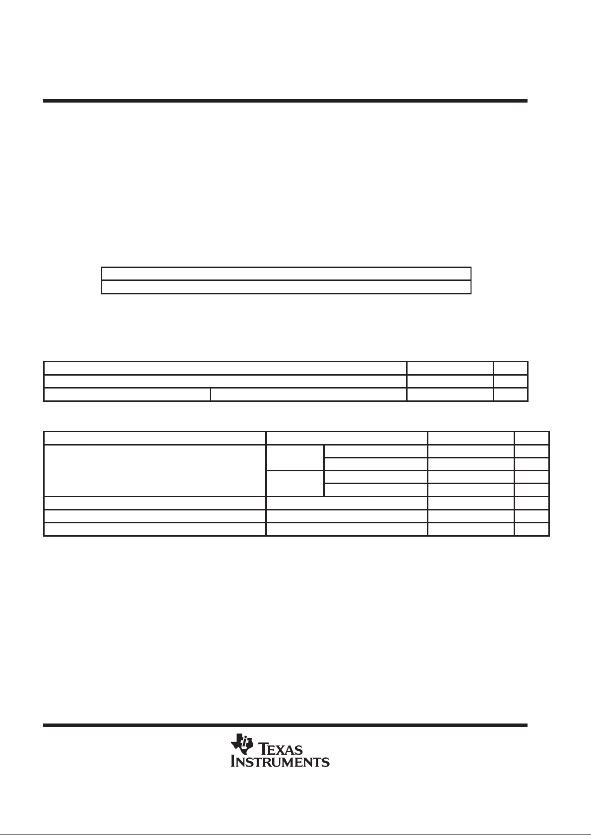
absolute maximum ratings over operating free-air temperature range (unless otherwise noted)
†
Supply voltage, VDD 6 V. . . . . . . . . . . . . . . . . . . . . . . . . . . . . . . . . . . . . . . . . . . . . . . . . . . . . . . . . . . . . . . . . . . . . . . .
Continuous output current (COUT+, COUT–, LOUT, ROUT) 2 A. . . . . . . . . . . . . . . . . . . . . . . . . . . . . . . . . . . . . .
Continuous total power dissipation internally limited. . . . . . . . . . . . . . . . . . . . . . . . . . . . . . . . . . . . . . . . . . . . . . . . .
Operating virtual junction temperature range, T
J
–40°C to 150°C. . . . . . . . . . . . . . . . . . . . . . . . . . . . . . . . . . . . .
Operating virtual case temperature range, TC –40°C to 125°C. . . . . . . . . . . . . . . . . . . . . . . . . . . . . . . . . . . . . . .
Storage temperature range, T
stg
–65°C to 150°C. . . . . . . . . . . . . . . . . . . . . . . . . . . . . . . . . . . . . . . . . . . . . . . . . . .
Lead temperature 1,6 mm (1/16 inch) from case for 10 seconds 260°C. . . . . . . . . . . . . . . . . . . . . . . . . . . . . .
†
Stresses beyond those listed under “absolute maximum ratings” may cause permanent damage to the device. These are stress ratings only, and
functional operation of the device at these or any other conditions beyond those indicated under “recommended operating conditions” is not
implied. Exposure to absolute-maximum-rated conditions for extended periods may affect device reliability.
DISSIPATION RATING TABLE
PACKAGE
TA ≤ 25°C DERA TING FACTOR TA = 70°C TA = 85°C
PWP
‡
2.7 W 21.8 mW/°C 1.7 W 1.4 W
‡
Please see the Texas Instruments document,
PowerPAD Thermally Enhanced Package Application Report
(literature number SLMA002), for more information on the PowerPAD package. The thermal data was
measured on a PCB layout based on the information in the section entitled
T exas Instruments Recommended
Board for PowerPAD
on page 33 of the before mentioned document.
recommended operating conditions
MIN NOM MAX UNIT
Supply Voltage, V
DD
3 5 5.5 V
Operating junction temperature, T
J
125 °C
dc electrical characteristics, TA = 25°C
PARAMETER TEST CONDITIONS NOM TYP MAX UNIT
3 Channel 19 25 mA
pp
V
DD
= 5
V
L and R or Center only 9 15 mA
IDDSupply current
3 Channel 13 20 mA
V
DD
= 3.3
V
L and R or Center only 3 10 mA
V
OO
Output offset voltage (measured differentially) VDD = 5 V, Gain = 2, See Note 1 5 35 mV
I
DD(MUTE)
Supply current in mute mode VDD = 5 V 800 µA
I
DD(SD)
IDD in shutdown VDD = 5 V 5 15 µA
NOTE 1: At 3 V < VDD < 5 V the dc output voltage is approximately VDD/2.
TPA0103
1.75-W 3-CHANNEL STEREO AUDIO POWER AMPLIFIER
SLOS167A – JULY 1997 – REVISED MARCH 2000
5
POST OFFICE BOX 655303 • DALLAS, TEXAS 75265
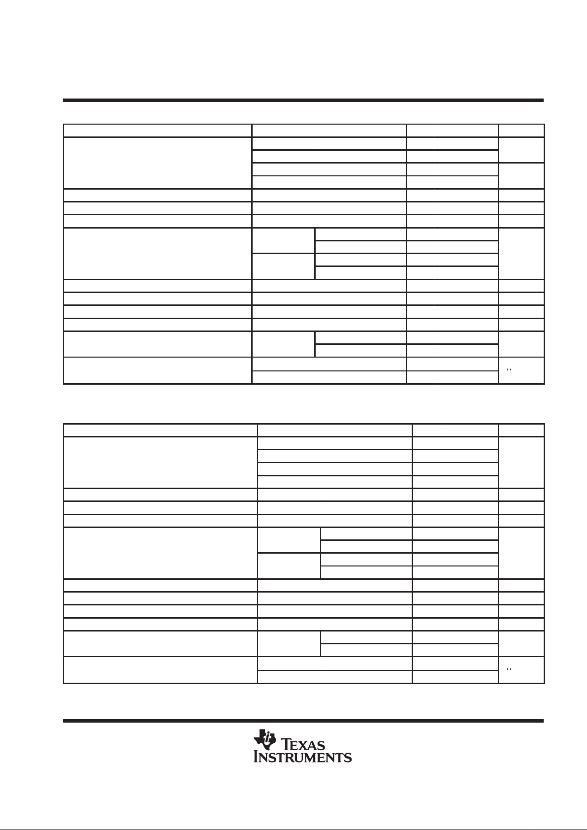
ac operating characteristics, V
DD
= 5 V, T
A
= 25°C, R
L
= 4 Ω
PARAMETER TEST CONDITIONS MIN TYP MAX UNIT
THD = 0.2%, BTL, Center channel 1.75
p
p
THD = 1%, BTL, Center channel 2.1
W
POOutput power (each channel) (see Note 2)
THD = 0.2%, SE, L/R channels 535
THD = 1%, SE, L/R channels 575
mW
THD+N Total harmonic distortion plus noise Po = 1.5 W, f = 20 to 20 kHz 0.25%
B
OM
Maximum output power bandwidth G = 10, THD < 5 % >20 kHz
Phase margin Open loop 85 °
Center channel 80
pp
pp
f
= 1 kHz
L/R channels 58
Supply ripple rejection ratio
Center channel 60
dB
f
= 20 – 20 kHz
L/R channels 30
Mute attenuation 85 dB
Channel-to-channel output separation f = 1 kHz 95 dB
Line/HP input separation 100 dB
Z
I
Input impedance 2 MΩ
BTL, Center channel 94
Signal-to-noise ratio
V
O
= 1
V(rms)
SE, L/R channels 100
dB
p
BTL, Center channel 20
VnOutput noise voltage
SE, L/R channels 9
µ
V(rms)
NOTE 2: Output power is measured at the output terminals of the IC at 1 kHz.
ac operating characteristics, V
DD
= 3.3 V, TA = 25°C, RL = 4 Ω
PARAMETER TEST CONDITIONS MIN TYP MAX UNIT
THD = 0.2% BTL, Center channel 800
p
p
THD = 1% BTL, Center channel 850
POOutput power (each channel) (see Note 2)
THD = 0.2%, SE, L/R channels 215
mW
THD = 1%, SE, L/R channels 235
THD+N Total harmonic distortion plus noise Po = 750 mW, f = 20 to 20 kHz 0.8%
B
OM
Maximum output power bandwidth G = 10, THD < 5 % >20 kHz
Phase margin Open loop 85 °
Center channel 70
pp
pp
f
= 1 kHz
L/R channels 62
Supply ripple rejection ratio
Center channel 55
dB
f
= 20 – 20 kHz
L/R channels 30
Mute attenuation 85 dB
Channel-to-channel output separation f = 1 kHz 95 dB
Line/HP input separation 100 dB
Z
I
Input impedance 2 MΩ
BTL, Center channel 93
Signal-to-noise ratio
V
O
= 1
V(rms)
SE, L/R channels 100
dB
p
BTL, Center channel 21
VnOutput noise voltage
SE, L/R channels 10
µ
V(rms)
NOTE 2: Output power is measured at the output terminals of the IC at 1 kHz.
TPA0103
1.75-W 3-CHANNEL STEREO AUDIO POWER AMPLIFIER
SLOS167A – JULY 1997 – REVISED MARCH 2000
6
POST OFFICE BOX 655303 • DALLAS, TEXAS 75265
PARAMETER MEASUREMENT INFORMATION
R
I
C
I
R
F
C
B
4.7 µF
RL = 4 Ω or 8 Ω
V
DD
MODE A
MODE B
V
DD
HP/LINE
MUX
MUX
SHUTDOWN
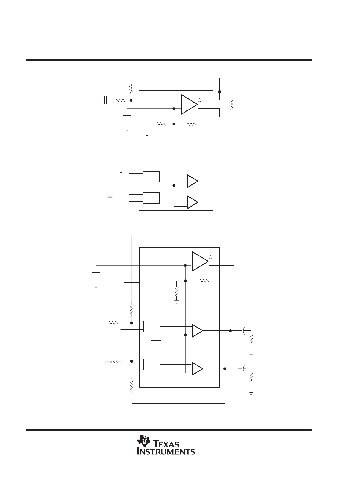
Figure 1. BTL Test Circuit
R
F
C
B
4.7 µF
V
DD
MODE A
MODE B
V
DD
HP/LINE
MUX
MUX
R
I
C
I
R
I
C
I
R
F
C
O
R
L
C
O
R
L
V
DD
SHUTDOWN
Figure 2. SE Test Circuit
TPA0103
1.75-W 3-CHANNEL STEREO AUDIO POWER AMPLIFIER
SLOS167A – JULY 1997 – REVISED MARCH 2000
7
POST OFFICE BOX 655303 • DALLAS, TEXAS 75265
TYPICAL CHARACTERISTICS
Table of Graphs
FIGURE
vs Output power
3, 4, 7, 10–12, 15, 18, 21, 24,
27, 30, 33, 36
THD + N Total harmonic distortion plus noise
vs Frequency
5, 6, 8, 9, 13, 14, 16, 17, 19,
20, 22, 23, 25, 26, 28, 29, 31,
32, 34, 35
V
n
Output noise voltage vs Frequency 37,38
Supply ripple rejection ratio vs Frequency 39, 40
Crosstalk vs Frequency 41, 42
Open loop response vs Frequency 43, 44
Closed loop response vs Frequency 45 – 48
I
DD
Supply current vs Supply voltage 49
P
O
Output power
vs Supply voltage
vs Load resistance
50, 51
52, 53
P
D
Power dissipation vs Output power 54 – 57
Figure 3
0.1
0.01
0 0.25 0.5 0.75 1 1.25 1.5
1
10
1.75 2 2.25 2.5
PO – Output Power – W
VDD = 5 V
f = 1 kHz
BTL
THD+N –Total Harmonic Distortion + Noise – %
TOTAL HARMONIC DISTORTION PLUS NOISE
vs
OUTPUT POWER
RL = 4 Ω
RL = 8 Ω
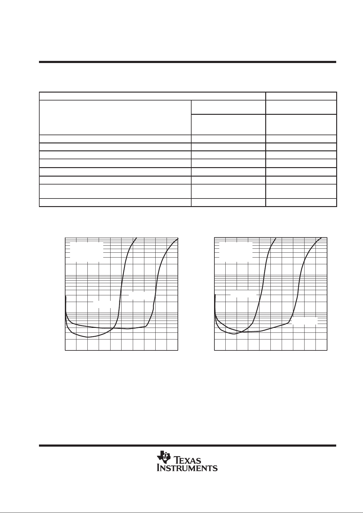
Figure 4
PO – Output Power – mW
THD+N –Total Harmonic Distortion + Noise – %
TOTAL HARMONIC DISTORTION PLUS NOISE
vs
OUTPUT POWER
0.1
0.01
0 75 150 225 300 375 450
1
10
525 600 675 750
VDD = 5 V
f = 1 kHz
SE
RL = 4 Ω
RL = 8 Ω
TPA0103
1.75-W 3-CHANNEL STEREO AUDIO POWER AMPLIFIER
SLOS167A – JULY 1997 – REVISED MARCH 2000
8
POST OFFICE BOX 655303 • DALLAS, TEXAS 75265
TYPICAL CHARACTERISTICS
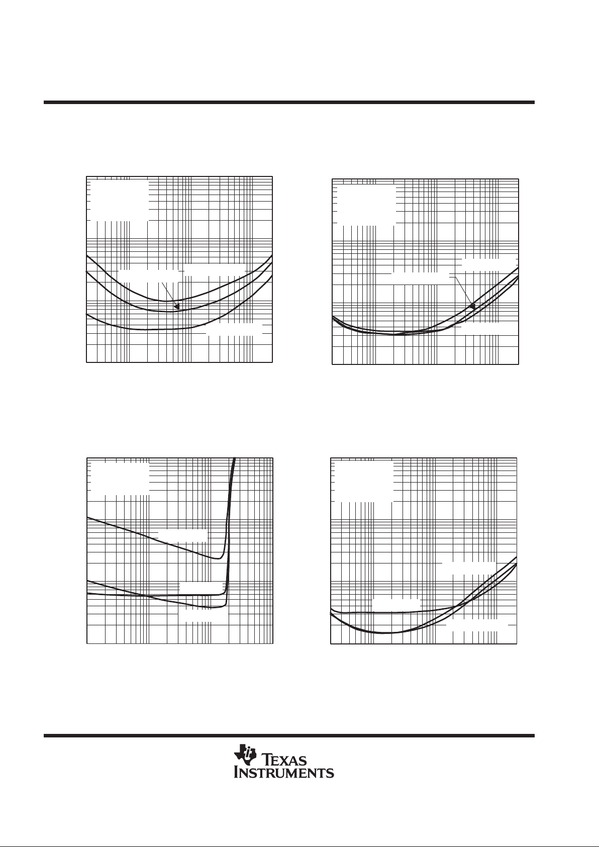
Figure 5
0.01
10
20 100 1 k 10 k 20 k
THD+N –Total Harmonic Distortion + Noise – %
f – Frequency – Hz
TOTAL HARMONIC DISTORTION PLUS NOISE
vs
FREQUENCY
1
0.1
VDD = 5 V
PO = 1.5 W
RL = 4 Ω
BTL
AV = –2 V/V
AV = –20 V/V
AV = –10 V/V
Figure 6
PO = 1.5 W
PO = 0.25 W
VDD = 5 V
RL = 4 Ω
AV = –2 V/V
BTL
0.1
0.01
20 100 1 k
1
10
10 k 20 k
THD+N –Total Harmonic Distortion + Noise – %
f – Frequency – Hz
TOTAL HARMONIC DISTORTION PLUS NOISE
vs
FREQUENCY
PO = 0.75 W
Figure 7
f = 20 kHz
f = 1 kHz
f = 20 Hz
0.1
0.01
0.01 0.1
1
10
110
PO – Output Power – W
VDD = 5 V
RL = 4 Ω
BTL
THD+N –Total Harmonic Distortion + Noise – %
TOTAL HARMONIC DISTORTION PLUS NOISE
vs
OUTPUT POWER
Figure 8
0.1
0.01
20 100 1 k
1
10
10 k 20 k
THD+N –Total Harmonic Distortion + Noise – %
f – Frequency – Hz
TOTAL HARMONIC DISTORTION PLUS NOISE
vs
FREQUENCY
PO = 1 W
VDD = 5 V
RL = 8 Ω
AV = –2 V/V
BTL
PO = 0.25 W
PO = 0.5 W
TPA0103
1.75-W 3-CHANNEL STEREO AUDIO POWER AMPLIFIER
SLOS167A – JULY 1997 – REVISED MARCH 2000
9
POST OFFICE BOX 655303 • DALLAS, TEXAS 75265
TYPICAL CHARACTERISTICS
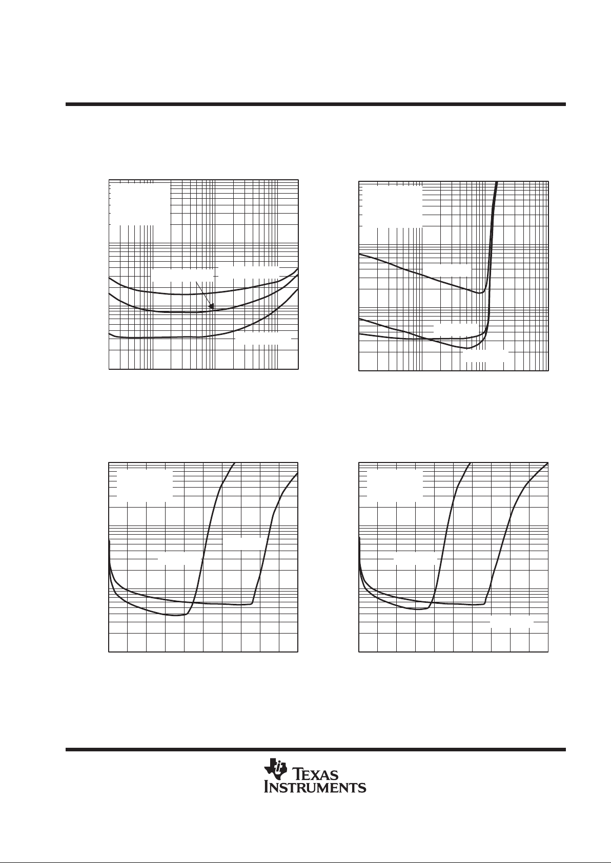
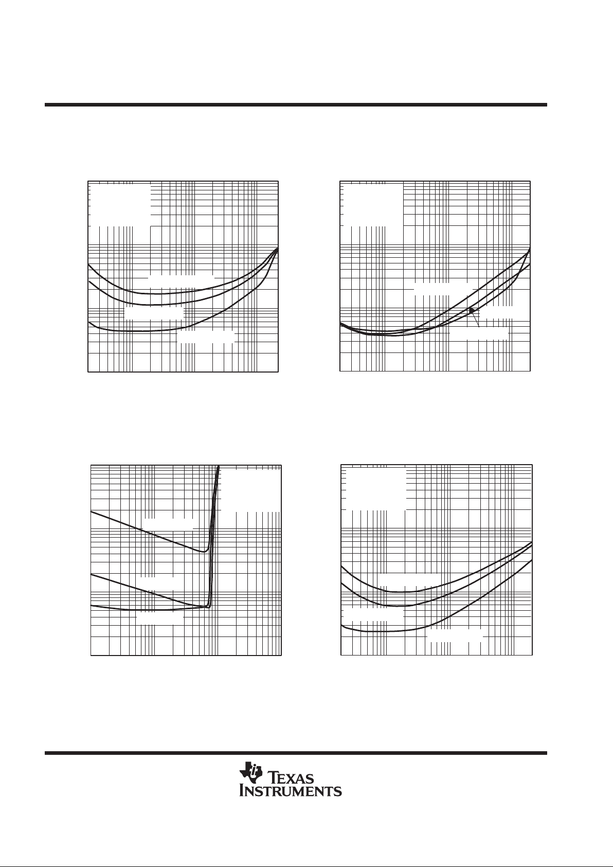
Figure 9
0.1
0.01
20 100 1 k
1
10
10 k 20 k
THD+N –Total Harmonic Distortion + Noise – %
f – Frequency – Hz
TOTAL HARMONIC DISTORTION PLUS NOISE
vs
FREQUENCY
VDD = 5 V
PO = 1 W
RL = 8 Ω
BTL
AV = –2 V/V
AV = –20 V/V
AV = –10 V/V
Figure 10
0.1
0.01
0.01 0.1
1
10
110
f = 20 kHz
f = 1 kHz
f = 20 Hz
PO – Output Power – W
VDD = 5 V
RL = 8 Ω
AV = –2 V/V
BTL
THD+N –Total Harmonic Distortion + Noise – %
TOTAL HARMONIC DISTORTION PLUS NOISE
vs
OUTPUT POWER
Figure 11
0.1
0.01
0 0.1 0.2 0.3 0.4 0.5 0.6
1
10
0.7 0.8 0.9 1
PO – Output Power – W
VDD = 3.3 V
f = 1 kHz
BTL
THD+N –Total Harmonic Distortion + Noise – %
TOTAL HARMONIC DISTORTION PLUS NOISE
vs
OUTPUT POWER
RL = 4 Ω
RL = 8 Ω
Figure 12
0.1
0.01
0 30 60 90 120 150 180
1
10
210 240 270 300
PO – Output Power – mW
VDD = 3.3 V
f = 1 kHz
SE
THD+N –Total Harmonic Distortion + Noise – %
TOTAL HARMONIC DISTORTION PLUS NOISE
vs
OUTPUT POWER
RL = 4 Ω
RL = 8 Ω
TPA0103
1.75-W 3-CHANNEL STEREO AUDIO POWER AMPLIFIER
SLOS167A – JULY 1997 – REVISED MARCH 2000
10
POST OFFICE BOX 655303 • DALLAS, TEXAS 75265
TYPICAL CHARACTERISTICS
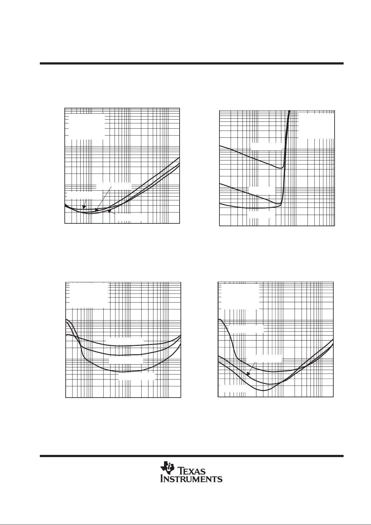
Figure 13
0.1
0.01
20 100 1 k
1
10
10 k 20 k
THD+N –Total Harmonic Distortion + Noise – %
f – Frequency – Hz
TOTAL HARMONIC DISTORTION PLUS NOISE
vs
FREQUENCY
VDD = 3.3 V
PO = 0.75 W
RL = 4 Ω
BTL
AV = –10 V/V
AV = –20 V/V
AV = –2 V/V
Figure 14
PO = 0.35 W
PO = 0.1 W
PO = 0.75 W
0.1
0.01
20 100 1 k
1
10
10 k 20 k
THD+N –Total Harmonic Distortion + Noise – %
f – Frequency – Hz
TOTAL HARMONIC DISTORTION PLUS NOISE
vs
FREQUENCY
VDD = 3.3 V
RL = 4 Ω
AV = –2 V/V
BTL
Figure 15
0.1
0.01
0.01
1
10
1100.1
f = 20 kHz
f = 1 kHz
f = 20 Hz
PO – Output Power – W
VDD = 3.3 V
RL = 4 Ω
AV = –2 V/V
BTL
THD+N –Total Harmonic Distortion + Noise – %
TOTAL HARMONIC DISTORTION PLUS NOISE
vs
OUTPUT POWER
Figure 16
0.1
0.01
20 100 1 k
1
10
10 k 20 k
THD+N –Total Harmonic Distortion + Noise – %
f – Frequency – Hz
TOTAL HARMONIC DISTORTION PLUS NOISE
vs
FREQUENCY
AV = –20 V/V
AV = –10 V/V
AV = –2 V/V
VDD = 3.3 V
PO = 0.4 W
RL = 8 Ω
BTL
TPA0103
1.75-W 3-CHANNEL STEREO AUDIO POWER AMPLIFIER
SLOS167A – JULY 1997 – REVISED MARCH 2000
11
POST OFFICE BOX 655303 • DALLAS, TEXAS 75265
TYPICAL CHARACTERISTICS
Figure 17
PO = 0.4 W
PO = 0.25 W
PO = 0.1 W
VDD = 3.3 V
RL = 8 Ω
AV = –2 V/V
BTL
0.1
0.01
20 100 1 k
1
10
10 k 20 k
THD+N –Total Harmonic Distortion + Noise – %
f – Frequency – Hz
TOTAL HARMONIC DISTORTION PLUS NOISE
vs
FREQUENCY
Figure 18
0.1
0.01
0.01 0.1
1
10
110
f = 20 kHz
f = 1 kHz
f = 20 Hz
PO – Output Power – W
VDD = 3.3 V
RL = 8 Ω
AV = –2 V/V
BTL
THD+N –Total Harmonic Distortion + Noise – %
TOTAL HARMONIC DISTORTION PLUS NOISE
vs
OUTPUT POWER
Figure 19
0.1
0.01
20 100 1 k
1
10
10 k 20 k
AV = –10 V/V
AV = –5 V/V
AV = –1 V/V
THD+N –Total Harmonic Distortion + Noise – %
f – Frequency – Hz
TOTAL HARMONIC DISTORTION PLUS NOISE
vs
FREQUENCY
VDD = 5 V
PO = 0.5 W
RL = 4 Ω
SE
Figure 20
0.1
0.01
20 100 1 k
1
10
10 k 20 k
PO = 0.25 W
PO = 0.1 W
PO = 0.5 W
THD+N –Total Harmonic Distortion + Noise – %
f – Frequency – Hz
TOTAL HARMONIC DISTORTION PLUS NOISE
vs
FREQUENCY
VDD = 5 V
RL = 4 Ω
AV = –2 V/V
SE
TPA0103
1.75-W 3-CHANNEL STEREO AUDIO POWER AMPLIFIER
SLOS167A – JULY 1997 – REVISED MARCH 2000
12
POST OFFICE BOX 655303 • DALLAS, TEXAS 75265
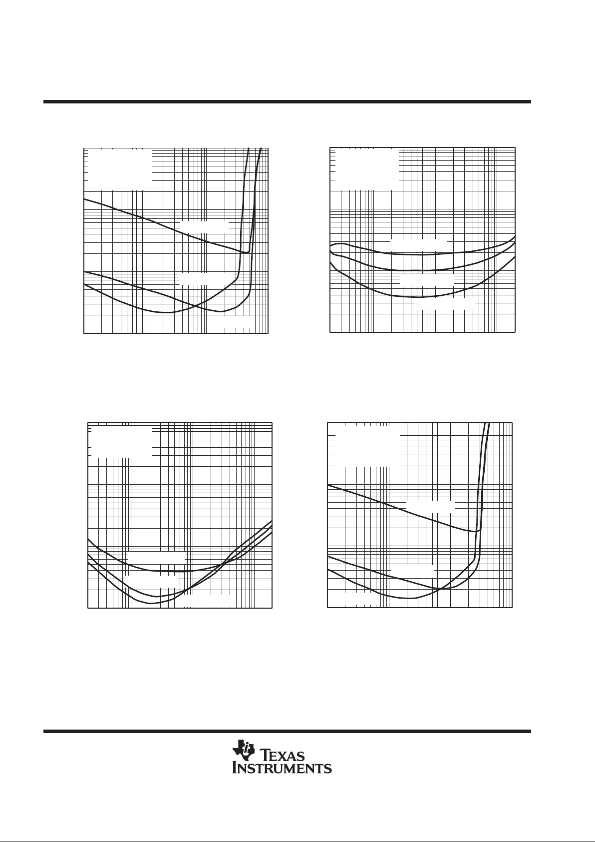
Figure 21
f = 20 kHz
f =100 Hz
f = 1 kHz
VDD = 5 V
RL = 4 Ω
AV = –2 V/V
SE
0.1
0.01
0.001 0.01
1
10
0.1 1
PO – Output Power – W
THD+N –Total Harmonic Distortion + Noise – %
TOTAL HARMONIC DISTORTION PLUS NOISE
vs
OUTPUT POWER
Figure 22
0.1
0.01
20 100 1 k
1
10
10 k 20 k
AV = –10 V/V
AV = –5 V/V
AV = –1 V/V
THD+N –Total Harmonic Distortion + Noise – %
f – Frequency – Hz
TOTAL HARMONIC DISTORTION PLUS NOISE
vs
FREQUENCY
VDD = 5 V
PO = 0.25 W
RL = 8 Ω
SE
Figure 23
0.1
0.01
20 100 1 k
1
10
10 k 20 k
PO = 0.25 W
PO = 0.05 W
PO = 0.1 W
THD+N –Total Harmonic Distortion + Noise – %
f – Frequency – Hz
TOTAL HARMONIC DISTORTION PLUS NOISE
vs
FREQUENCY
VDD = 5 V
RL = 8 Ω
SE
Figure 24
0.1
0.01
0.001 0.1
1
10
1
PO – Output Power – W
VDD = 5 V
RL = 8 Ω
AV = –2 V/V
SE
THD+N –Total Harmonic Distortion + Noise – %
TOTAL HARMONIC DISTORTION PLUS NOISE
vs
OUTPUT POWER
0.01
f = 20 kHz
f = 1 kHz
f = 100 Hz
 Loading...