


Please be aware that an important notice concerning availability, standard warranty, and use in critical applications of
Texas Instruments semiconductor products and disclaimers thereto appears at the end of this data sheet.
TP A0103
1.75-W 3-CHANNEL STEREO AUDIO POWER AMPLIFIER
SLOS167A – JULY 1997 – REVISED MARCH 2000
1
POST OFFICE BOX 655303 • DALLAS, TEXAS 75265
D
Desktop Computer Amplifier Solution
– 1.75-W Bridge Tied Load (BTL) Center
Channel
– 500-mW L/R Single-Ended Channels
D
Low Distortion Output
– < 0.05% THD+N at Full Power
D
Full 3.3-V and 5-V Specifications
D
Surface-Mount Power Package
24-Pin TSSOP
D
L/R Input MUX Feature
D
Shutdown Control ...I
DD
= 5 µA
C
B
Left
MUX
LHPIN
LLINEIN
+
–
BYPASS
COUT+
COUT–
MODE A
HP/LINE
R
FC
C
FC
R
IL
R
FL
V
DD
R
M1
R
M2
MODE B
V
DD
V
DD
CNTL
C
OUTR
R
M3
Right
MUX
C
OUTL
RHPIN
RLINEIN
NC
NC
R
FR
R
IR
C
IL
C
IR
R
IRC
R
ILC
+
–
+
–
MUTE OUT
NC
SHUTDOWN
CIN
10
6
19
9
8
20
21
5
4
15
14
11
7, 18
16
22
3
ROUT
LOUT
GND/HS
1, 12, 13, 24
Internal
Speaker
V
DD
1
2
3
4
5
6
7
8
9
10
11
12
24
23
22
21
20
19
18
17
16
15
14
13
GND/HS
NC
LOUT
LLINEIN
LHPIN
CIN
V
DD
SHUTDOWN
MUTE OUT
COUT+
MODE B
GND/HS
GND/HS
NC
ROUT
RLINEIN
RHPIN
BYPASS
V
DD
NC
HP/LINE
COUT–
MODE A
GND/HS
PWP PACKAGE
(TOP VIEW)
Copyright 2000, Texas Instruments Incorporated
PRODUCTION DATA information is current as of publication date.
Products conform to specifications per the terms of Texas Instruments
standard warranty. Production processing does not necessarily include
testing of all parameters.
PowerPAD is a trademark of Texas Instruments Incorporated.
TPA0103
1.75-W 3-CHANNEL STEREO AUDIO POWER AMPLIFIER
SLOS167A – JULY 1997 – REVISED MARCH 2000
2
POST OFFICE BOX 655303 • DALLAS, TEXAS 75265
description
The TPA0103 is a 3-channel audio power amplifier in a 24-pin TSSOP thermal package primarily targeted at
desktop PC or notebook applications. The left/right (L/R) channel outputs are single ended (SE) and capable
of delivering 500 mW of continuous RMS power per channel into 4-Ω loads. The center channel output is a
bridged tied load (BTL) configuration for delivering maximum output power from PC power supplies. Combining
the SE line drivers and high power center channel amplifiers in a single TSSOP package simplifies design and
frees up board space for other features. Full power distortion levels of less than 0.25% THD+N into 4-Ω loads
from a 5-V supply voltage are typical. Low-voltage application are also well served by the TP A0103 providing
800 mW to the center channel into 4-Ω loads with a 3.3-V supply voltage.
Amplifier gain is externally configured by means of two resistors per input channel and does not require external
compensation for settings of 1 to 10. A two channel input MUX circuit is integrated on the L/R channel inputs
to allow two sets of stereo inputs to the amplifier. In the typical application, the center channel amplifier is driven
from a mix of the L/R inputs to produce a monaural representation of the stereo signal. The center channel
amplifier can be shut down independently of the L/R output for speaker muting in headphone applications. The
TPA0103 also features a full shutdown function for power sensitive applications holding the bias current
to 5 µA.
The PowerPAD package (PWP) delivers a level of thermal performance that was previously achievable only
in TO-220-type packages. Thermal impedances of less than 35°C/W are readily realized in multilayer PCB
applications. This allows the TPA0103 to operate at full power at ambient temperature of up to 85°C.
AVAILABLE OPTIONS
PACKAGE
T
A
TSSOP
†
(PWP)
–40°C to 85°C TPA0103PWP
†
The PWP package is available in left-ended tape
and reel only (e.g., TPA0103PWPLE).
TPA0103
1.75-W 3-CHANNEL STEREO AUDIO POWER AMPLIFIER
SLOS167A – JULY 1997 – REVISED MARCH 2000
3
POST OFFICE BOX 655303 • DALLAS, TEXAS 75265
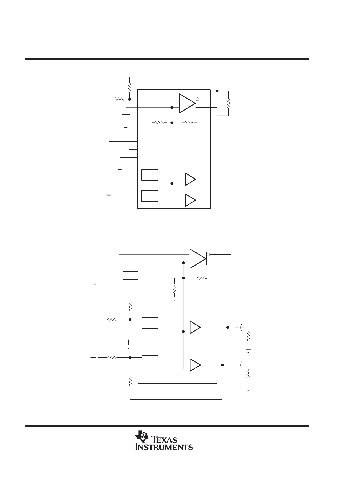
Terminal Functions
TERMINAL
NAME NO.
I/O
DESCRIPTION
BYPASS 19 Bypass. BYPASS is a tap to the voltage divider for the internal mid-supply bias.
CIN 6 I Center channel input
COUT+ 10 O Center channel + output. COUT+ is in an active or high-impedance state unless the device is in a mute state
when the MODE A terminal (14) is high and the MODE B terminal (11) is low.
COUT– 15 O Center channel – output. COUT– is in an active or high-impedance state unless the device is in a mute state
when the MODE A terminal (14) is high and the MODE B terminal (11) is low.
GND/HS 1, 12,
13, 24
Ground. GND/HS is the ground connection for circuitry, directly connected to thermal pad.
MODE A, 14, 11 I
Mode select. MODE A and MODE B determine the output modes of the TPA0103.
MODE B
TERMINAL 3 CHANNEL MUTE CENTER
ONLY
L/R
ONLY
MODE A L H L H
MODE B L L H H
HP/LINE 16 I Input MUX control input, hold high to select (L/R) HPIN (5, 20), hold low to select (L/R) LINEIN (4, 21). HP/LINE
is normally connected to ground when inputs are connected to (L/R) LINEIN.
LHPIN 5 I Left channel headphone input, selected when the HP/LINE terminal (16) is held high
LLINEIN 4 I Left channel line input, selected when the HP/LINE terminal (16) is held low
LOUT 3 O Left channel output. LOUT is active when the MODE A terminal (14) is low and the MODE B terminal (11) is
don’t care.
MUTE OUT 9 O When the MODE A terminal (14) is high and the MODE B terminal (11) is low , MUTE OUT is high and the device
is in a mute state. Otherwise MUTE OUT is low.
NC 2, 17,
23
No internal connection
RHPIN 20 I Right channel headphone input, selected when the HP/LINE terminal (16) is held high
RLINEIN 21 I Right channel line input, selected when the HP/LINE terminal (16) is held low
ROUT 22 O Right channel output. ROUT is active when the MODE A terminal (14) is low and the MODE B terminal (11)
is don’t care.
SHUTDOWN 8 I Places entire IC in shutdown mode when held high, I
DD
= 5 µA
V
DD
7, 18 I Supply voltage input. The VDD terminals must be connected together.
TPA0103
1.75-W 3-CHANNEL STEREO AUDIO POWER AMPLIFIER
SLOS167A – JULY 1997 – REVISED MARCH 2000
4
POST OFFICE BOX 655303 • DALLAS, TEXAS 75265
absolute maximum ratings over operating free-air temperature range (unless otherwise noted)
†
Supply voltage, VDD 6 V. . . . . . . . . . . . . . . . . . . . . . . . . . . . . . . . . . . . . . . . . . . . . . . . . . . . . . . . . . . . . . . . . . . . . . . .
Continuous output current (COUT+, COUT–, LOUT, ROUT) 2 A. . . . . . . . . . . . . . . . . . . . . . . . . . . . . . . . . . . . . .
Continuous total power dissipation internally limited. . . . . . . . . . . . . . . . . . . . . . . . . . . . . . . . . . . . . . . . . . . . . . . . .
Operating virtual junction temperature range, T
J
–40°C to 150°C. . . . . . . . . . . . . . . . . . . . . . . . . . . . . . . . . . . . .
Operating virtual case temperature range, TC –40°C to 125°C. . . . . . . . . . . . . . . . . . . . . . . . . . . . . . . . . . . . . . .
Storage temperature range, T
stg
–65°C to 150°C. . . . . . . . . . . . . . . . . . . . . . . . . . . . . . . . . . . . . . . . . . . . . . . . . . .
Lead temperature 1,6 mm (1/16 inch) from case for 10 seconds 260°C. . . . . . . . . . . . . . . . . . . . . . . . . . . . . .
†
Stresses beyond those listed under “absolute maximum ratings” may cause permanent damage to the device. These are stress ratings only, and
functional operation of the device at these or any other conditions beyond those indicated under “recommended operating conditions” is not
implied. Exposure to absolute-maximum-rated conditions for extended periods may affect device reliability.
DISSIPATION RATING TABLE
PACKAGE
TA ≤ 25°C DERA TING FACTOR TA = 70°C TA = 85°C
PWP
‡
2.7 W 21.8 mW/°C 1.7 W 1.4 W
‡
Please see the Texas Instruments document,
PowerPAD Thermally Enhanced Package Application Report
(literature number SLMA002), for more information on the PowerPAD package. The thermal data was
measured on a PCB layout based on the information in the section entitled
T exas Instruments Recommended
Board for PowerPAD
on page 33 of the before mentioned document.
recommended operating conditions
MIN NOM MAX UNIT
Supply Voltage, V
DD
3 5 5.5 V
Operating junction temperature, T
J
125 °C
dc electrical characteristics, TA = 25°C
PARAMETER TEST CONDITIONS NOM TYP MAX UNIT
3 Channel 19 25 mA
pp
V
DD
= 5
V
L and R or Center only 9 15 mA
IDDSupply current
3 Channel 13 20 mA
V
DD
= 3.3
V
L and R or Center only 3 10 mA
V
OO
Output offset voltage (measured differentially) VDD = 5 V, Gain = 2, See Note 1 5 35 mV
I
DD(MUTE)
Supply current in mute mode VDD = 5 V 800 µA
I
DD(SD)
IDD in shutdown VDD = 5 V 5 15 µA
NOTE 1: At 3 V < VDD < 5 V the dc output voltage is approximately VDD/2.
TPA0103
1.75-W 3-CHANNEL STEREO AUDIO POWER AMPLIFIER
SLOS167A – JULY 1997 – REVISED MARCH 2000
5
POST OFFICE BOX 655303 • DALLAS, TEXAS 75265
ac operating characteristics, V
DD
= 5 V, T
A
= 25°C, R
L
= 4 Ω
PARAMETER TEST CONDITIONS MIN TYP MAX UNIT
THD = 0.2%, BTL, Center channel 1.75
p
p
THD = 1%, BTL, Center channel 2.1
W
POOutput power (each channel) (see Note 2)
THD = 0.2%, SE, L/R channels 535
THD = 1%, SE, L/R channels 575
mW
THD+N Total harmonic distortion plus noise Po = 1.5 W, f = 20 to 20 kHz 0.25%
B
OM
Maximum output power bandwidth G = 10, THD < 5 % >20 kHz
Phase margin Open loop 85 °
Center channel 80
pp
pp
f
= 1 kHz
L/R channels 58
Supply ripple rejection ratio
Center channel 60
dB
f
= 20 – 20 kHz
L/R channels 30
Mute attenuation 85 dB
Channel-to-channel output separation f = 1 kHz 95 dB
Line/HP input separation 100 dB
Z
I
Input impedance 2 MΩ
BTL, Center channel 94
Signal-to-noise ratio
V
O
= 1
V(rms)
SE, L/R channels 100
dB
p
BTL, Center channel 20
VnOutput noise voltage
SE, L/R channels 9
µ
V(rms)
NOTE 2: Output power is measured at the output terminals of the IC at 1 kHz.
ac operating characteristics, V
DD
= 3.3 V, TA = 25°C, RL = 4 Ω
PARAMETER TEST CONDITIONS MIN TYP MAX UNIT
THD = 0.2% BTL, Center channel 800
p
p
THD = 1% BTL, Center channel 850
POOutput power (each channel) (see Note 2)
THD = 0.2%, SE, L/R channels 215
mW
THD = 1%, SE, L/R channels 235
THD+N Total harmonic distortion plus noise Po = 750 mW, f = 20 to 20 kHz 0.8%
B
OM
Maximum output power bandwidth G = 10, THD < 5 % >20 kHz
Phase margin Open loop 85 °
Center channel 70
pp
pp
f
= 1 kHz
L/R channels 62
Supply ripple rejection ratio
Center channel 55
dB
f
= 20 – 20 kHz
L/R channels 30
Mute attenuation 85 dB
Channel-to-channel output separation f = 1 kHz 95 dB
Line/HP input separation 100 dB
Z
I
Input impedance 2 MΩ
BTL, Center channel 93
Signal-to-noise ratio
V
O
= 1
V(rms)
SE, L/R channels 100
dB
p
BTL, Center channel 21
VnOutput noise voltage
SE, L/R channels 10
µ
V(rms)
NOTE 2: Output power is measured at the output terminals of the IC at 1 kHz.
TPA0103
1.75-W 3-CHANNEL STEREO AUDIO POWER AMPLIFIER
SLOS167A – JULY 1997 – REVISED MARCH 2000
6
POST OFFICE BOX 655303 • DALLAS, TEXAS 75265
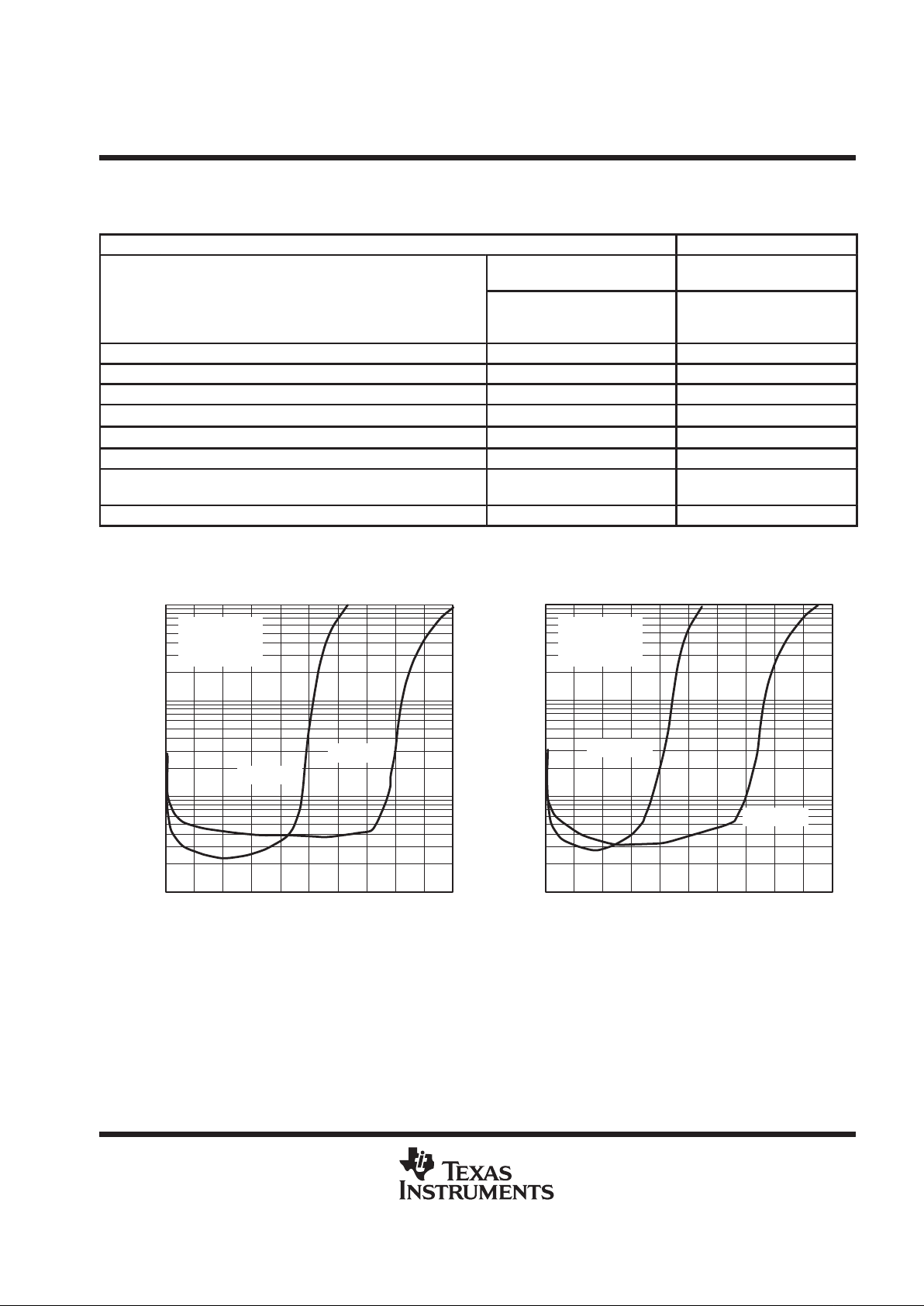
PARAMETER MEASUREMENT INFORMATION
R
I
C
I
R
F
C
B
4.7 µF
RL = 4 Ω or 8 Ω
V
DD
MODE A
MODE B
V
DD
HP/LINE
MUX
MUX
SHUTDOWN
Figure 1. BTL Test Circuit
R
F
C
B
4.7 µF
V
DD
MODE A
MODE B
V
DD
HP/LINE
MUX
MUX
R
I
C
I
R
I
C
I
R
F
C
O
R
L
C
O
R
L
V
DD
SHUTDOWN
Figure 2. SE Test Circuit
TPA0103
1.75-W 3-CHANNEL STEREO AUDIO POWER AMPLIFIER
SLOS167A – JULY 1997 – REVISED MARCH 2000
7
POST OFFICE BOX 655303 • DALLAS, TEXAS 75265
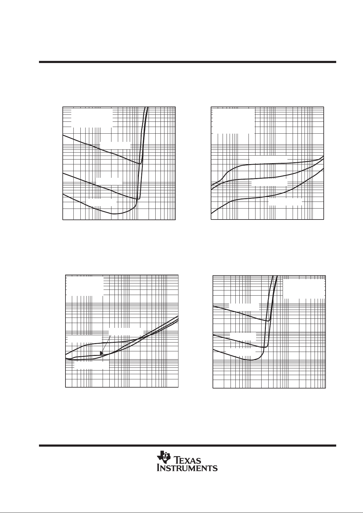
TYPICAL CHARACTERISTICS
Table of Graphs
FIGURE
vs Output power
3, 4, 7, 10–12, 15, 18, 21, 24,
27, 30, 33, 36
THD + N Total harmonic distortion plus noise
vs Frequency
5, 6, 8, 9, 13, 14, 16, 17, 19,
20, 22, 23, 25, 26, 28, 29, 31,
32, 34, 35
V
n
Output noise voltage vs Frequency 37,38
Supply ripple rejection ratio vs Frequency 39, 40
Crosstalk vs Frequency 41, 42
Open loop response vs Frequency 43, 44
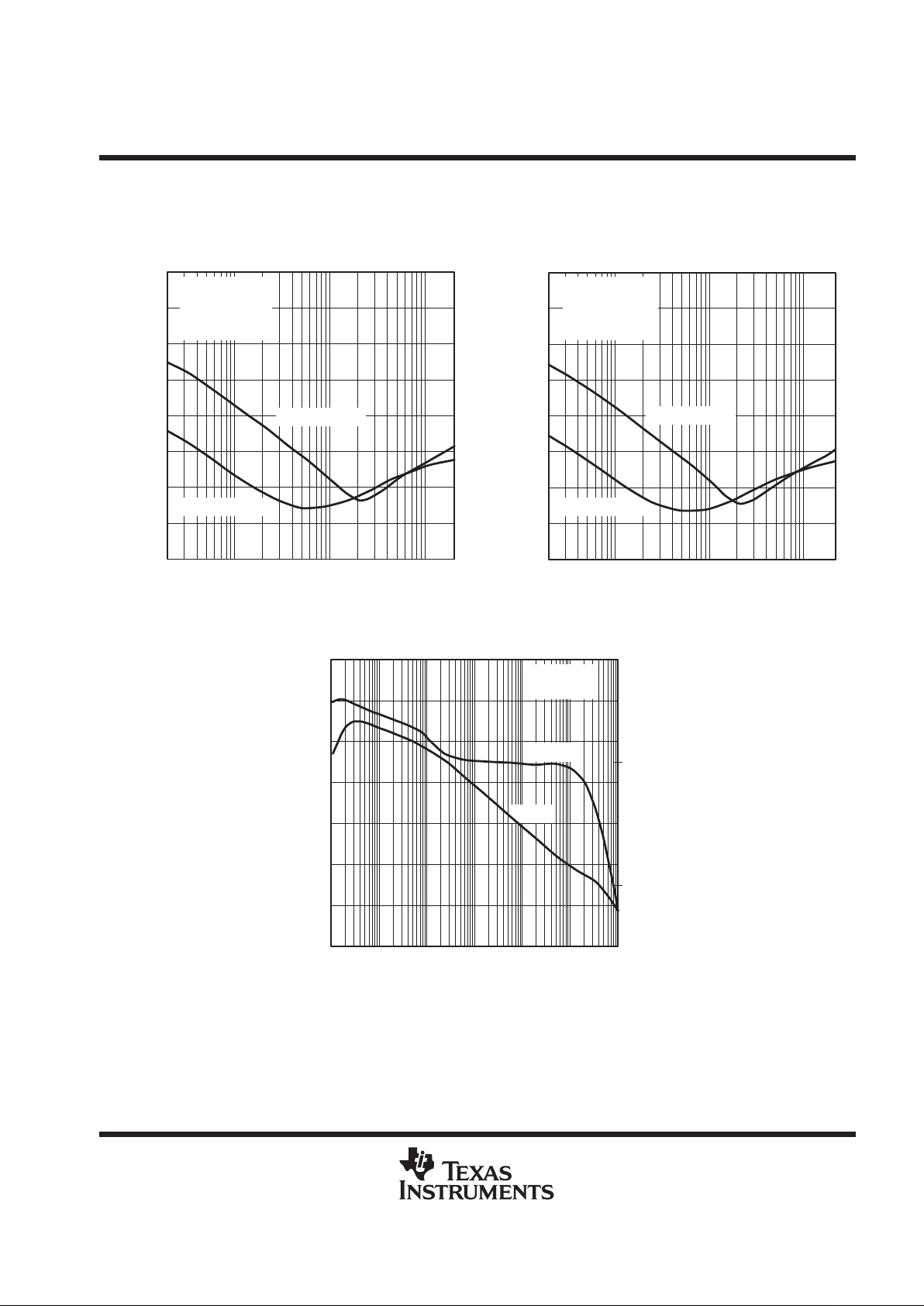
Closed loop response vs Frequency 45 – 48
I
DD
Supply current vs Supply voltage 49
P
O
Output power
vs Supply voltage
vs Load resistance
50, 51
52, 53
P
D
Power dissipation vs Output power 54 – 57
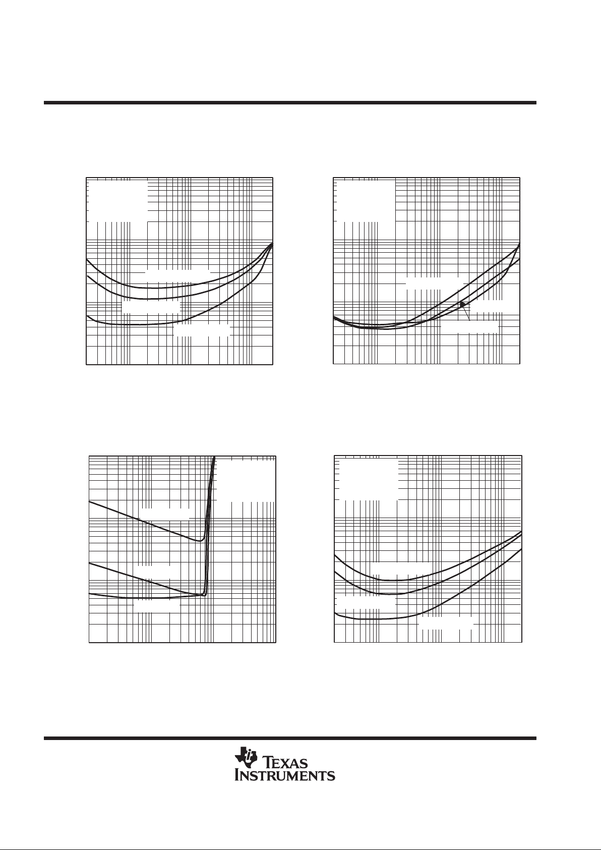
Figure 3
0.1
0.01
0 0.25 0.5 0.75 1 1.25 1.5
1
10
1.75 2 2.25 2.5
PO – Output Power – W
VDD = 5 V
f = 1 kHz
BTL
THD+N –Total Harmonic Distortion + Noise – %
TOTAL HARMONIC DISTORTION PLUS NOISE
vs
OUTPUT POWER
RL = 4 Ω
RL = 8 Ω
Figure 4
PO – Output Power – mW
THD+N –Total Harmonic Distortion + Noise – %
TOTAL HARMONIC DISTORTION PLUS NOISE
vs
OUTPUT POWER
0.1
0.01
0 75 150 225 300 375 450
1
10
525 600 675 750
VDD = 5 V
f = 1 kHz
SE
RL = 4 Ω
RL = 8 Ω
TPA0103
1.75-W 3-CHANNEL STEREO AUDIO POWER AMPLIFIER
SLOS167A – JULY 1997 – REVISED MARCH 2000
8
POST OFFICE BOX 655303 • DALLAS, TEXAS 75265
TYPICAL CHARACTERISTICS
Figure 5
0.01
10
20 100 1 k 10 k 20 k
THD+N –Total Harmonic Distortion + Noise – %
f – Frequency – Hz
TOTAL HARMONIC DISTORTION PLUS NOISE
vs
FREQUENCY
1
0.1
VDD = 5 V
PO = 1.5 W
RL = 4 Ω
BTL
AV = –2 V/V
AV = –20 V/V
AV = –10 V/V
Figure 6
PO = 1.5 W
PO = 0.25 W
VDD = 5 V
RL = 4 Ω
AV = –2 V/V
BTL
0.1
0.01
20 100 1 k
1
10
10 k 20 k
THD+N –Total Harmonic Distortion + Noise – %
f – Frequency – Hz
TOTAL HARMONIC DISTORTION PLUS NOISE
vs
FREQUENCY
PO = 0.75 W
Figure 7
f = 20 kHz
f = 1 kHz
f = 20 Hz
0.1
0.01
0.01 0.1
1
10
110
PO – Output Power – W
VDD = 5 V
RL = 4 Ω
BTL
THD+N –Total Harmonic Distortion + Noise – %
TOTAL HARMONIC DISTORTION PLUS NOISE
vs
OUTPUT POWER
Figure 8
0.1
0.01
20 100 1 k
1
10
10 k 20 k
THD+N –Total Harmonic Distortion + Noise – %
f – Frequency – Hz
TOTAL HARMONIC DISTORTION PLUS NOISE
vs
FREQUENCY
PO = 1 W
VDD = 5 V
RL = 8 Ω
AV = –2 V/V
BTL
PO = 0.25 W
PO = 0.5 W
TPA0103
1.75-W 3-CHANNEL STEREO AUDIO POWER AMPLIFIER
SLOS167A – JULY 1997 – REVISED MARCH 2000
9
POST OFFICE BOX 655303 • DALLAS, TEXAS 75265
TYPICAL CHARACTERISTICS
Figure 9
0.1
0.01
20 100 1 k
1
10
10 k 20 k
THD+N –Total Harmonic Distortion + Noise – %
f – Frequency – Hz
TOTAL HARMONIC DISTORTION PLUS NOISE
vs
FREQUENCY
VDD = 5 V
PO = 1 W
RL = 8 Ω
BTL
AV = –2 V/V
AV = –20 V/V
AV = –10 V/V
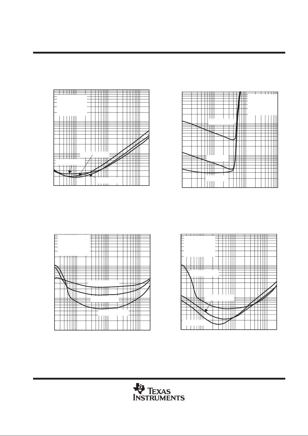
Figure 10
0.1
0.01
0.01 0.1
1
10
110
f = 20 kHz
f = 1 kHz
f = 20 Hz
PO – Output Power – W
VDD = 5 V
RL = 8 Ω
AV = –2 V/V
BTL
THD+N –Total Harmonic Distortion + Noise – %
TOTAL HARMONIC DISTORTION PLUS NOISE
vs
OUTPUT POWER
Figure 11
0.1
0.01
0 0.1 0.2 0.3 0.4 0.5 0.6
1
10
0.7 0.8 0.9 1
PO – Output Power – W
VDD = 3.3 V
f = 1 kHz
BTL
THD+N –Total Harmonic Distortion + Noise – %
TOTAL HARMONIC DISTORTION PLUS NOISE
vs
OUTPUT POWER
RL = 4 Ω
RL = 8 Ω
Figure 12
0.1
0.01
0 30 60 90 120 150 180
1
10
210 240 270 300
PO – Output Power – mW
VDD = 3.3 V
f = 1 kHz
SE
THD+N –Total Harmonic Distortion + Noise – %
TOTAL HARMONIC DISTORTION PLUS NOISE
vs
OUTPUT POWER
RL = 4 Ω
RL = 8 Ω
TPA0103
1.75-W 3-CHANNEL STEREO AUDIO POWER AMPLIFIER
SLOS167A – JULY 1997 – REVISED MARCH 2000
10
POST OFFICE BOX 655303 • DALLAS, TEXAS 75265
TYPICAL CHARACTERISTICS
Figure 13
0.1
0.01
20 100 1 k
1
10
10 k 20 k
THD+N –Total Harmonic Distortion + Noise – %
f – Frequency – Hz
TOTAL HARMONIC DISTORTION PLUS NOISE
vs
FREQUENCY
VDD = 3.3 V
PO = 0.75 W
RL = 4 Ω
BTL
AV = –10 V/V
AV = –20 V/V
AV = –2 V/V
Figure 14
PO = 0.35 W
PO = 0.1 W
PO = 0.75 W
0.1
0.01
20 100 1 k
1
10
10 k 20 k
THD+N –Total Harmonic Distortion + Noise – %
f – Frequency – Hz
TOTAL HARMONIC DISTORTION PLUS NOISE
vs
FREQUENCY
VDD = 3.3 V
RL = 4 Ω
AV = –2 V/V
BTL
Figure 15
0.1
0.01
0.01
1
10
1100.1
f = 20 kHz
f = 1 kHz
f = 20 Hz
PO – Output Power – W
VDD = 3.3 V
RL = 4 Ω
AV = –2 V/V
BTL
THD+N –Total Harmonic Distortion + Noise – %
TOTAL HARMONIC DISTORTION PLUS NOISE
vs
OUTPUT POWER
Figure 16
0.1
0.01
20 100 1 k
1
10
10 k 20 k
THD+N –Total Harmonic Distortion + Noise – %
f – Frequency – Hz
TOTAL HARMONIC DISTORTION PLUS NOISE
vs
FREQUENCY
AV = –20 V/V
AV = –10 V/V
AV = –2 V/V
VDD = 3.3 V
PO = 0.4 W
RL = 8 Ω
BTL
TPA0103
1.75-W 3-CHANNEL STEREO AUDIO POWER AMPLIFIER
SLOS167A – JULY 1997 – REVISED MARCH 2000
11
POST OFFICE BOX 655303 • DALLAS, TEXAS 75265
TYPICAL CHARACTERISTICS
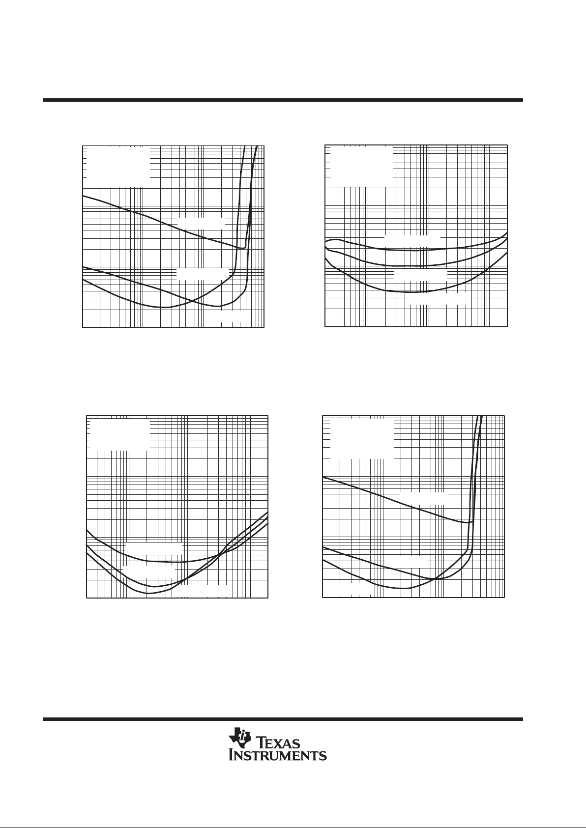
Figure 17
PO = 0.4 W
PO = 0.25 W
PO = 0.1 W
VDD = 3.3 V
RL = 8 Ω
AV = –2 V/V
BTL
0.1
0.01
20 100 1 k
1
10
10 k 20 k
THD+N –Total Harmonic Distortion + Noise – %
f – Frequency – Hz
TOTAL HARMONIC DISTORTION PLUS NOISE
vs
FREQUENCY
Figure 18
0.1
0.01
0.01 0.1
1
10
110
f = 20 kHz
f = 1 kHz
f = 20 Hz
PO – Output Power – W
VDD = 3.3 V
RL = 8 Ω
AV = –2 V/V
BTL
THD+N –Total Harmonic Distortion + Noise – %
TOTAL HARMONIC DISTORTION PLUS NOISE
vs
OUTPUT POWER
Figure 19
0.1
0.01
20 100 1 k
1
10
10 k 20 k
AV = –10 V/V
AV = –5 V/V
AV = –1 V/V
THD+N –Total Harmonic Distortion + Noise – %
f – Frequency – Hz
TOTAL HARMONIC DISTORTION PLUS NOISE
vs
FREQUENCY
VDD = 5 V
PO = 0.5 W
RL = 4 Ω
SE
Figure 20
0.1
0.01
20 100 1 k
1
10
10 k 20 k
PO = 0.25 W
PO = 0.1 W
PO = 0.5 W
THD+N –Total Harmonic Distortion + Noise – %
f – Frequency – Hz
TOTAL HARMONIC DISTORTION PLUS NOISE
vs
FREQUENCY
VDD = 5 V
RL = 4 Ω
AV = –2 V/V
SE
TPA0103
1.75-W 3-CHANNEL STEREO AUDIO POWER AMPLIFIER
SLOS167A – JULY 1997 – REVISED MARCH 2000
12
POST OFFICE BOX 655303 • DALLAS, TEXAS 75265
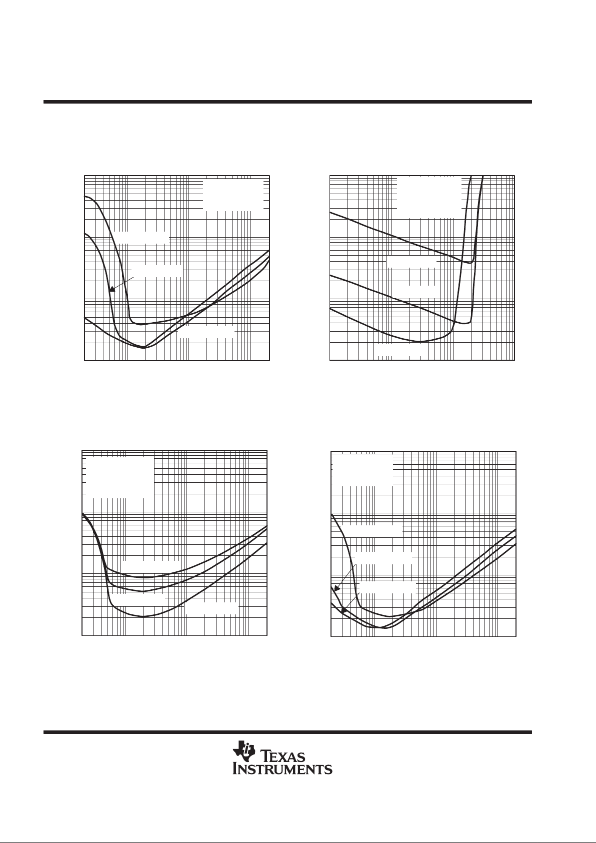
Figure 21
f = 20 kHz
f =100 Hz
f = 1 kHz
VDD = 5 V
RL = 4 Ω
AV = –2 V/V
SE
0.1
0.01
0.001 0.01
1
10
0.1 1
PO – Output Power – W
THD+N –Total Harmonic Distortion + Noise – %
TOTAL HARMONIC DISTORTION PLUS NOISE
vs
OUTPUT POWER
Figure 22
0.1
0.01
20 100 1 k
1
10
10 k 20 k
AV = –10 V/V
AV = –5 V/V
AV = –1 V/V
THD+N –Total Harmonic Distortion + Noise – %
f – Frequency – Hz
TOTAL HARMONIC DISTORTION PLUS NOISE
vs
FREQUENCY
VDD = 5 V
PO = 0.25 W
RL = 8 Ω
SE
Figure 23
0.1
0.01
20 100 1 k
1
10
10 k 20 k
PO = 0.25 W
PO = 0.05 W
PO = 0.1 W
THD+N –Total Harmonic Distortion + Noise – %
f – Frequency – Hz
TOTAL HARMONIC DISTORTION PLUS NOISE
vs
FREQUENCY
VDD = 5 V
RL = 8 Ω
SE
Figure 24
0.1
0.01
0.001 0.1
1
10
1
PO – Output Power – W
VDD = 5 V
RL = 8 Ω
AV = –2 V/V
SE
THD+N –Total Harmonic Distortion + Noise – %
TOTAL HARMONIC DISTORTION PLUS NOISE
vs
OUTPUT POWER
0.01
f = 20 kHz
f = 1 kHz
f = 100 Hz

TPA0103
1.75-W 3-CHANNEL STEREO AUDIO POWER AMPLIFIER
SLOS167A – JULY 1997 – REVISED MARCH 2000
13
POST OFFICE BOX 655303 • DALLAS, TEXAS 75265
TYPICAL CHARACTERISTICS
Figure 25
0.1
0.01
20 100 1 k
1
10
10 k 20 k
AV = –10 V/V
AV = –5 V/V
AV = –1 V/V
THD+N –Total Harmonic Distortion + Noise – %
f – Frequency – Hz
TOTAL HARMONIC DISTORTION PLUS NOISE
vs
FREQUENCY
VDD = 5 V
PO = 75 mW
RL = 32 Ω
SE
Figure 26
0.1
0.01
20 100 1 k
1
10
10 k 20 k
PO = 75 mW
PO = 25 mW
PO = 50 mW
THD+N –Total Harmonic Distortion + Noise – %
f – Frequency – Hz
TOTAL HARMONIC DISTORTION PLUS NOISE
vs
FREQUENCY
VDD = 5 V
RL = 32 Ω
SE
Figure 27
0.1
0.01
0.001 0.01
1
10
0.1 1
f = 20 kHz
f = 1 kHz
f = 20 Hz
PO – Output Power – W
VDD = 5 V
RL = 32 Ω
SE
THD+N –Total Harmonic Distortion + Noise – %
TOTAL HARMONIC DISTORTION PLUS NOISE
vs
OUTPUT POWER
Figure 28
0.1
0.01
20 100 1 k
1
10
10 k 20 k
AV = –10 V/V
AV = –5 V/V
AV = –1 V/V
THD+N –Total Harmonic Distortion + Noise – %
f – Frequency – Hz
TOTAL HARMONIC DISTORTION PLUS NOISE
vs
FREQUENCY
VDD = 3.3 V
PO = 0.2 W
RL = 4 Ω
SE
TPA0103
1.75-W 3-CHANNEL STEREO AUDIO POWER AMPLIFIER
SLOS167A – JULY 1997 – REVISED MARCH 2000
14
POST OFFICE BOX 655303 • DALLAS, TEXAS 75265
TYPICAL CHARACTERISTICS
Figure 29
0.1
0.01
20 100 1 k
1
10
10 k 20 k
PO = 0.05 W
PO = 0.1 W
PO = 0.2 W
THD+N –Total Harmonic Distortion + Noise – %
f – Frequency – Hz
TOTAL HARMONIC DISTORTION PLUS NOISE
vs
FREQUENCY
VDD = 3.3 V
RL = 4 Ω
SE
Figure 30
f = 100 Hz
f = 1 kHz
f = 20 kHz
VDD = 3.3 V
RL = 4 Ω
AV = –2 V/V
SE
0.1
0.01
0.001 0.01
1
10
10.1
PO – Output Power – W
THD+N –Total Harmonic Distortion + Noise – %
TOTAL HARMONIC DISTORTION PLUS NOISE
vs
OUTPUT POWER
Figure 31
AV = –10 V/V
AV = –5 V/V
AV = –1 V/V
VDD = 3.3 V
PO = 100 mW
RL = 8 Ω
SE
0.1
0.01
20 100 1 k
1
10
10 k 20 k
THD+N –Total Harmonic Distortion + Noise – %
f – Frequency – Hz
TOTAL HARMONIC DISTORTION PLUS NOISE
vs
FREQUENCY
Figure 32
0.1
0.01
20 100 1 k
1
10
10 k 20 k
PO = 25 mW
PO = 50 mW
PO = 100 mW
THD+N –Total Harmonic Distortion + Noise – %
f – Frequency – Hz
TOTAL HARMONIC DISTORTION PLUS NOISE
vs
FREQUENCY
VDD = 3.3 V
RL = 8 Ω
SE
TPA0103
1.75-W 3-CHANNEL STEREO AUDIO POWER AMPLIFIER
SLOS167A – JULY 1997 – REVISED MARCH 2000
15
POST OFFICE BOX 655303 • DALLAS, TEXAS 75265
TYPICAL CHARACTERISTICS
Figure 33
VDD = 3.3 V
RL = 8 Ω
SE
0.1
0.01
0.001 0.1
1
10
1
PO – Output Power – W
THD+N –Total Harmonic Distortion + Noise – %
TOTAL HARMONIC DISTORTION PLUS NOISE
vs
OUTPUT POWER
f = 20 kHz
f = 1 kHz
f = 100 Hz
0.01
Figure 34
0.1
0.01
20 100 1 k
1
10
10 k 20 k
AV = –10 V/V
AV = –5 V/V
AV = –1 V/V
THD+N –Total Harmonic Distortion + Noise – %
f – Frequency – Hz
TOTAL HARMONIC DISTORTION PLUS NOISE
vs
FREQUENCY
VDD = 3.3 V
PO = 30 mW
RL = 32 Ω
SE
Figure 35
0.1
0.01
0.001
20 100 1 k
1
10
10 k 20 k
PO = 10 mW
PO = 20 mW
PO = 30 mW
THD+N –Total Harmonic Distortion + Noise – %
f – Frequency – Hz
TOTAL HARMONIC DISTORTION PLUS NOISE
vs
FREQUENCY
VDD = 3.3 V
RL = 32 Ω
SE
Figure 36
0.1
0.01
0.001
0.001 0.01
1
10
0.1 1
f = 20 Hz
f = 1 kHz
f = 20 kHz
PO – Output Power – W
VDD = 3.3 V
RL = 32 Ω
SE
THD+N –Total Harmonic Distortion + Noise – %
TOTAL HARMONIC DISTORTION PLUS NOISE
vs
OUTPUT POWER
TPA0103
1.75-W 3-CHANNEL STEREO AUDIO POWER AMPLIFIER
SLOS167A – JULY 1997 – REVISED MARCH 2000
16
POST OFFICE BOX 655303 • DALLAS, TEXAS 75265
TYPICAL CHARACTERISTICS
Figure 37
10
1
20 100 1 k
f – Frequency – Hz
OUTPUT NOISE VOLTAGE
vs
FREQUENCY
100
10 k 20 k
VDD = 5 V
BW = 22 Hz to 22 kHz
RL = 4Ω
– Output Noise Voltage –
V
n
V(rms)
µ
Center
Left
Right
Figure 38
10
1
20 100 1 k
f – Frequency – Hz
OUTPUT NOISE VOLTAGE
vs
FREQUENCY
100
10 k 20 k
VDD = 3.3 V
BW = 22 Hz to 22 kHz
RL = 4Ω
Center
Left
Right
– Output Noise Voltage –
V
n
V(rms)
µ
Figure 39
–50
–60
–80
–100
20 100 1 k
–30
–20
f – Frequency – Hz
SUPPLY RIPPLE REJECTION RATIO
vs
FREQUENCY
0
10 k 20 k
–10
–40
–70
–90
VDD = 5 V
VDD = 3.3 V
RL = 4 Ω
CB = 4.7 µF
BTL
Supply Ripple Rejection Ratio – dB
Figure 40
–50
–60
–80
–100
20 100 1 k
–30
–20
f – Frequency – Hz
SUPPLY RIPPLE REJECTION RATIO
vs
FREQUENCY
0
10 k 20 k
–10
–40
–70
–90
VDD = 5 V
VDD = 3.3 V
RL = 4 Ω
CB = 4.7 µF
SE
Supply Ripple Rejection Ratio – dB
TPA0103
1.75-W 3-CHANNEL STEREO AUDIO POWER AMPLIFIER
SLOS167A – JULY 1997 – REVISED MARCH 2000
17
POST OFFICE BOX 655303 • DALLAS, TEXAS 75265
TYPICAL CHARACTERISTICS
Figure 41
–80
–90
–110
–120
–60
–50
–40
–70
–100
20 100 1 k
Crosstalk – dB
f – Frequency – Hz
CROSSTALK
vs
FREQUENCY
10 k 20 k
VDD = 5 V
PO = 75 mW
RL = 32 Ω
SE
Left to Right
Right to Left
Figure 42
–80
–90
–110
–120
–60
–50
–40
–70
–100
20 100 1 k
Crosstalk – dB
f – Frequency – Hz
CROSSTALK
vs
FREQUENCY
10 k 20 k
VDD = 3.3 V
PO = 35 mW
RL = 32 Ω
SE
Left to Right
Right to Left
40
20
–20
–40
0.01
Gain – dB
60
80
f – Frequency – kHz
OPEN LOOP RESPONSE
100
0
0.1 1 10 100 1000 10000
180°
90°
0°
–90°
–180°
VDD = 5 V
BTL
Gain
Phase
Figure 43
Phase

TPA0103
1.75-W 3-CHANNEL STEREO AUDIO POWER AMPLIFIER
SLOS167A – JULY 1997 – REVISED MARCH 2000
18
POST OFFICE BOX 655303 • DALLAS, TEXAS 75265
TYPICAL CHARACTERISTICS
20
0
–20
–40
40
60
80
180°
90°
0°
–90°
–180°
0.01
Gain – dB
f – Frequency – kHz
OPEN LOOP RESPONSE
0.1 1 10 100 1000 10000
VDD = 3.3 V
BTL
Gain
Figure 44
Phase
Phase
5
3
2
0
20 100 1 k 10 k
Gain – dB
7
9
f – Frequency – Hz
CLOSED LOOP RESPONSE
10
100 k 200 k
8
6
4
1
–45°
0°
–90°
–135°
–180°
–225°
–270°
Phase
Phase
Gain
VDD = 5 V
AV = –2 V/V
PO = 1.5 W
BTL
Figure 45

TPA0103
1.75-W 3-CHANNEL STEREO AUDIO POWER AMPLIFIER
SLOS167A – JULY 1997 – REVISED MARCH 2000
19
POST OFFICE BOX 655303 • DALLAS, TEXAS 75265
TYPICAL CHARACTERISTICS
5
3
2
0
20 100 1 k 10 k
Gain – dB
7
9
f – Frequency – Hz
CLOSED LOOP RESPONSE
10
100 k 200 k
8
6
4
1
–45°
0°
–90°
–135°
–180°
–225°
–270°
Phase
Phase
Gain
VDD = 3.3 V
AV = –2 V/V
PO = 0.75 W
BTL
Figure 46
Figure 47
–5
–7
–8
–10
20 100 1 k 10 k
Gain – dB
–3
–1
f – Frequency – Hz
CLOSED LOOP RESPONSE
0
100 k 200 k
–2
–4
–6
–9
–45°
0°
–90°
–135°
–180°
–225°
–270°
Phase
VDD = 5 V
AV = –1 V/V
PO = 0.5 W
SE
Phase
Gain

TPA0103
1.75-W 3-CHANNEL STEREO AUDIO POWER AMPLIFIER
SLOS167A – JULY 1997 – REVISED MARCH 2000
20
POST OFFICE BOX 655303 • DALLAS, TEXAS 75265
TYPICAL CHARACTERISTICS
–5
–7
–8
–10
20 100 1 k 10 k
Gain – dB
–3
–1
f – Frequency – Hz
CLOSED LOOP RESPONSE
0
100 k 200 k
–2
–4
–6
–9
–45°
0°
–90°
–135°
–180°
–225°
–270°
Phase
VDD = 3.3V
AV = –1 V/V
PO = 0.25 W
SE
Phase
Gain
Figure 48
Figure 49
3 Channel
15
10
5
0
3
20
25
SUPPLY CURRENT
vs
SUPPLY VOLTAGE
30
465
VDD – Supply Voltage – V
L/R or Center
Channel
– Supply Current – mA
I
DD
Figure 50
1.5
1
0.5
0
2.5 3 3.5 4 4.5 5
2
2.5
3
5.5 6
RL = 4 Ω
RL = 8 Ω
– Output Power – WP
O
OUTPUT POWER
vs
SUPPLY VOLTAGE
VDD – Supply Voltage – V
THD+N = 1%
BTL
Center Channel

TPA0103
1.75-W 3-CHANNEL STEREO AUDIO POWER AMPLIFIER
SLOS167A – JULY 1997 – REVISED MARCH 2000
21
POST OFFICE BOX 655303 • DALLAS, TEXAS 75265
TYPICAL CHARACTERISTICS
Figure 51
0.4
0.2
0
2.5 3 3.5 4 4.5 5
0.6
0.8
1
5.5 6
RL = 4 Ω
RL = 8 Ω
RL = 32 Ω
THD+N = 1%
SE
Each L/R Channel
– Output Power – WP
O
OUTPUT POWER
vs
SUPPLY VOLTAGE
VDD – Supply Voltage – V
Figure 52
RL – Load Resistance – Ω
1.5
1
0.5
0
04 8121620
2
2.5
3
24 28 32
THD+N = 1%
BTL
Center Channel
– Output Power – WP
O
OUTPUT POWER
vs
LOAD RESISTANCE
VDD = 5 V
VDD = 3.3 V
Figure 53
0.4
0.2
0
04 8121620
0.6
0.8
1
24 28 32
RL – Load Resistance – Ω
THD+N = 1%
SE
Each L/R Channel
– Output Power – WP
O
OUTPUT POWER
vs
LOAD RESISTANCE
VDD = 5 V
VDD = 3.3 V
Figure 54
0.6
0.4
0.2
0
0 0.5 1
– Power Dissipation – W
1
1.2
POWER DISSIPATION
vs
OUTPUT POWER
1.4
1.5 2
0.8
PO – Output Power – W
P
D
RL = 4 Ω
RL = 8 Ω
VDD = 5 V
BTL
Center Channel

TPA0103
1.75-W 3-CHANNEL STEREO AUDIO POWER AMPLIFIER
SLOS167A – JULY 1997 – REVISED MARCH 2000
22
POST OFFICE BOX 655303 • DALLAS, TEXAS 75265
TYPICAL CHARACTERISTICS
Figure 55
0.4
0.2
0
0 0.1 0.2 0.3
0.6
0.8
0.4 0.5 0.6
– Power Dissipation – W
POWER DISSIPATION
vs
OUTPUT POWER
PO – Output Power – W
P
D
RL = 4 Ω
RL = 8 Ω
VDD = 5 V
SE
Each L/R Channel
RL = 32Ω
Figure 56
0.3
0.2
0.1
0
0 0.25 0.5
– Power Dissipation – W
0.4
0.5
POWER DISSIPATION
vs
OUTPUT POWER
0.6
0.75 1
PO – Output Power – W
P
D
RL = 4 Ω
RL = 8 Ω
VDD = 3.3 V
BTL
Center Channel
Figure 57
0.2
0
0 0.05 0.1 0.15
0.4
0.6
0.2 0.25
– Power Dissipation – W
POWER DISSIPATION
vs
OUTPUT POWER
PO – Output Power – W
P
D
RL = 4 Ω
RL = 8 Ω
VDD = 3.3V
SE
Each L/R Channel
RL = 32Ω

TPA0103
1.75-W 3-CHANNEL STEREO AUDIO POWER AMPLIFIER
SLOS167A – JULY 1997 – REVISED MARCH 2000
23
POST OFFICE BOX 655303 • DALLAS, TEXAS 75265
THERMAL INFORMATION
The thermally enhanced PWP package is based on the 24-pin TSSOP, but includes a thermal pad (see Figure 58)
to provide an effective thermal contact between the IC and the PWB.
Traditionally, surface mount and power have been mutually exclusive terms. A variety of scaled-down TO-220-type
packages have leads formed as gull wings to make them applicable for surface-mount applications. These packages,
however, have only two shortcomings: they do not address the very low profile requirements (<2 mm) of many of
today’s advanced systems, and they do not offer a terminal-count high enough to accommodate increasing
integration. On the other hand, traditional low-power surface-mount packages require power-dissipation derating that
severely limits the usable range of many high-performance analog circuits.
The PowerP AD package (thermally enhanced TSSOP) combines fine-pitch surface-mount technology with thermal
performance comparable to much larger power packages.
The PowerPAD package is designed to optimize the heat transfer to the PWB. Because of the very small size and
limited mass of a TSSOP package, thermal enhancement is achieved by improving the thermal conduction paths that
remove heat from the component. The thermal pad is formed using a patented lead-frame design and manufacturing
technique to provide a direct connection to the heat-generating IC. When this pad is soldered or otherwise thermally
coupled to an external heat dissipator, high power dissipation in the ultra-thin, fine-pitch, surface-mount package can
be reliably achieved.
DIE
Side View (a)
End View (b)
Bottom View (c)
DIE
Thermal
Pad
Figure 58. Views of Thermally Enhanced PWP Package

TPA0103
1.75-W 3-CHANNEL STEREO AUDIO POWER AMPLIFIER
SLOS167A – JULY 1997 – REVISED MARCH 2000
24
POST OFFICE BOX 655303 • DALLAS, TEXAS 75265
APPLICATION INFORMATION
bridged-tied load versus single-ended mode
Figure 59 shows a linear audio power amplifier (AP A) in a BTL configuration. The TPA0103 center -channel BTL
amplifier consists of two linear amplifiers driving both ends of the load. There are several potential benefits to
this differential drive configuration but initially consider power to the load. The differential drive to the speaker
means that as one side is slewing up the other side is slewing down and vice versa. This in effect doubles the
voltage swing on the load as compared to a ground referenced load. Plugging 2 × V
O(PP)
into the power
equation, where voltage is squared, yields 4× the output power from the same supply rail and load impedance
(see equation 1).
Power
+
V
(rms)
2
R
L
(1)
V
(rms)
+
V
O(PP)
22
Ǹ
R
L
2x V
O(PP)
V
O(PP)
–V
O(PP)
V
DD
V
DD
Figure 59. Bridge-Tied Load Configuration
In a typical computer sound channel operating at 5 V, bridging raises the power into an 8-Ω speaker from a
singled-ended (SE, ground reference) limit of 250 mW to 1 W. In sound power that is a 6-dB improvement —
which is loudness that can be heard. In addition to increased power there are frequency response concerns.
Consider the single-supply SE configuration of the L/R channels as shown in Figure 60. A coupling capacitor
is required to block the dc offset voltage from reaching the load. These capacitors can be quite large
(approximately 33 µF to 1000 µF) so they tend to be expensive, heavy, occupy valuable PCB area, and have
the additional drawback of limiting low-frequency performance of the system. This frequency limiting effect is
due to the high pass filter network created with the speaker impedance and the coupling capacitance and is
calculated with equation 2.

TPA0103
1.75-W 3-CHANNEL STEREO AUDIO POWER AMPLIFIER
SLOS167A – JULY 1997 – REVISED MARCH 2000
25
POST OFFICE BOX 655303 • DALLAS, TEXAS 75265
APPLICATION INFORMATION
fc+
1
2pR
L
C
C
(2)
For example, a 68-µF capacitor with an 8-Ω speaker would attenuate low frequencies below 293 Hz. The BTL
configuration cancels the dc offsets, which eliminates the need for the blocking capacitors. Low-frequency
performance is then limited only by the input network and speaker response. Cost and PCB space are also
minimized by eliminating the bulky coupling capacitor.
R
L
C
C
V
O(PP)
V
O(PP)
V
DD
–3 dB
f
c
fc = 293 Hz, 8 Ω, 68 µF
fc = 73 Hz, 32 Ω, 68 µF
Figure 60. Single-Ended Configuration and Frequency Response
BTL amplifier efficiency
Linear amplifiers are notoriously inefficient. The primary cause of these inefficiencies is voltage drop across the
output stage transistors. There are two components of the internal voltage drop. One is the headroom or dc
voltage drop that varies inversely to output power. The second component is due to the sinewave nature of the
output. The total voltage drop can be calculated by subtracting the RMS value of the output voltage from V
DD
.
The internal voltage drop multiplied by the RMS value of the supply current, IDDrms, determines the internal
power dissipation of the amplifier.
An easy-to-use equation to calculate efficiency starts out as being equal to the ratio of power from the power
supply to the power delivered to the load. To accurately calculate the RMS values of power in the load and in
the amplifier, the current and voltage waveform shapes must first be understood (see Figure 61).
V
(LRMS)
V
O
I
DD
I
DD(RMS)
Figure 61. Voltage and Current Waveforms for BTL Amplifiers

TPA0103
1.75-W 3-CHANNEL STEREO AUDIO POWER AMPLIFIER
SLOS167A – JULY 1997 – REVISED MARCH 2000
26
POST OFFICE BOX 655303 • DALLAS, TEXAS 75265
APPLICATION INFORMATION
Although the voltages and currents for SE and BTL are sinusoidal in the load, currents from the supply are very
different between SE and BTL configurations. In an SE application the current waveform is a half-wave rectified
shape whereas in BTL it is a full-wave rectified waveform. This means RMS conversion factors are different.
Keep in mind that for most of the waveform both the push and pull transistors are not on at the same time, which
supports the fact that each amplifier in the BTL device only draws current from the supply for half the waveform.
The following equations are the basis for calculating amplifier efficiency.
I
DD
rms
+
V
PP
p
R
L
P
SUP
+
VDDIDDrms
+
VDDV
PP
p
R
L
Efficiency
+
P
L
P
SUP
Efficiency of a BTE Configuration
+
P
L
P
SUP
+
V
PP
2
2R
L
p
R
L
VDDV
PP
+
V
PP
p
2V
DD
+
p
2PLR
L
Ǹ
2V
DD
(3)
Where:
(4)
P
L(BTL)
+
VLrms
2
R
L
+
V
PP
2
2R
L
,VPP+
PLRL2
Ǹ
VLrms(BTL)
+
V
PP
22
Ǹ
2+
V
PP
2
Ǹ
VPP+
2V
P
2VPP+
V
L
*
V
PP
Equation 4 can also be used for SE operations.
T able 1 employs equation 4 to calculate efficiencies for four different output power levels. Note that the efficiency
of the amplifier is quite low for lower power levels and rises sharply as power to the load is increased resulting
in a nearly flat internal power dissipation over the normal operating range. Note that the internal dissipation at
full output power is less than in the half power range. Calculating the efficiency for a specific system is the key
to proper power supply design. For a stereo 1-W audio system with 8-Ω loads and a 5-V supply , the maximum
draw on the power supply is almost 3.25 W.
Table 1. Efficiency Vs Output Power in 5-V 8-Ω BTL Systems
OUTPUT POWER
(W)
EFFICIENCY
(%)
PEAK-TO-PEAK
VOLTAGE
(V)
INTERNAL
DISSIPATION
(W)
0.25 31.4 2.00 0.55
0.50 44.4 2.83 0.62
1.00 62.8 4.00 0.59
1.25 70.2 4.47
†
0.53
†
High peak voltages cause the THD to increase.
A final point to remember about linear amplifiers (either SE or BTL) is how to manipulate the terms in the
efficiency equation to utmost advantage when possible. Note that in equation 4, VDD is in the denominator. This
indicates that as VDD goes down, efficiency goes up. As the numerator values of RL and PL decrease, efficiency
decreases.

TPA0103
1.75-W 3-CHANNEL STEREO AUDIO POWER AMPLIFIER
SLOS167A – JULY 1997 – REVISED MARCH 2000
27
POST OFFICE BOX 655303 • DALLAS, TEXAS 75265
APPLICATION INFORMATION
For example, if the 5-V supply is replaced with a 3.3-V supply (TP A0103 has a maximum recommended V
DD
of 5.5 V) in the calculations of Table 1 then efficiency at 0.5 W would rise from 44% to 67% and internal power
dissipation would fall from 0.62 W to 0.25 W at 5 V. Then for a stereo 0.5-W system from a 3.3-V supply, the
maximum draw would only be 1.5 W as compared to 2.24 W from 5 V . In other words, use the efficiency analysis
to chose the correct supply voltage and speaker impedance for the application.
selection of components
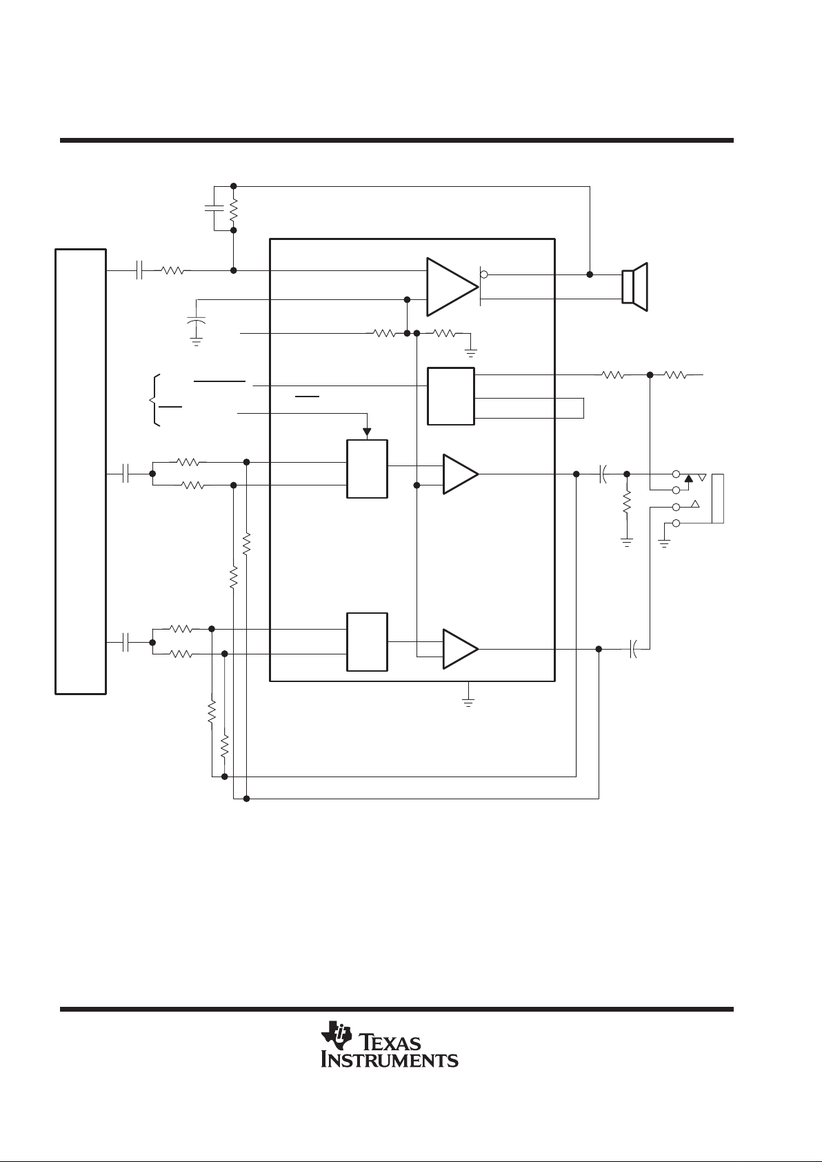
Figure 62 and Figure 63 are a schematic diagrams of typical computer application circuits.
C
B
Left
MUX
LHPIN
LLINEIN
+
–
BYPASS
COUT+
COUT–
MODE A
HP/LINE
R
FC
C
FC
R
IL
R
FL
V
DD
R
M1
100 kΩ
R
M2
100 kΩ
MODE B
V
DD
V
DD
CNTL
C
OUTR
R
M3
1 kΩ
Right
MUX
C
OUTL
RHPIN
RLINEIN
NC
NC
R
FR
R
IR
C
IL
C
IR
R
IRC
R
ILC
+
–
+
–
MUTE OUT
NC
SHUTDOWN
CIN
10
6
19
9
8
20
21
5
4
15
14
11
7, 18
16
22
3
ROUT
LOUT
GND/HS
1, 12, 13, 24
Internal
Speaker
V
DD
Figure 62. TPA0103 Minimum Configuration Application Circuit
TPA0103
1.75-W 3-CHANNEL STEREO AUDIO POWER AMPLIFIER
SLOS167A – JULY 1997 – REVISED MARCH 2000
28
POST OFFICE BOX 655303 • DALLAS, TEXAS 75265
APPLICATION INFORMATION
C
B
4.7 µF
Left
MUX
LHPIN
LLINEIN
+
–
BYPASS
COUT+
COUT–
MODE A
RFC
100 kΩ
C
FC
5 pF
R
ILL
10 kΩ
R
FLL
50 kΩ
V
DD
R
M1
100 kΩ
R
M2
100 kΩ
(see Note A)
MUTE OUT
V
DD
CNTL
C
OUTR
470 µF
R
M3
1 kΩ
Right
MUX
C
OUTL
470 µF
RHPIN
RLINEIN
R
FRL
50 kΩ
C
IL
0.1 µF
C
IR
0.1 µF
+
–
+
–
MODE B
HP/LINE
CIN
10
6
19
11
16
20
21
5
4
15
14
11
7, 18
22
3
ROUT
LOUT
GND/HS
1, 12, 13, 24
4 Ω
Internal
Speaker
Mono
AC97
Right
Line
C
IC
0.1 µF
R
IC
10 kΩ
R
ILHP
10 kΩ
R
IRHP
10 kΩ
R
IRL
10 kΩ
R
FRHP
10 kΩ
R
FLHP
10 kΩ
Active/Shutdown
High/Low Gain
System
Control
SHUTDOWN
8
Left
Line
4 Ω – 32 Ω
Speakers or
Headphones
V
DD
NOTE A: This connection is for ultralow current in shutdown mode.
Figure 63. TPA0103 Full Configuration Application Circuit

TPA0103
1.75-W 3-CHANNEL STEREO AUDIO POWER AMPLIFIER
SLOS167A – JULY 1997 – REVISED MARCH 2000
29
POST OFFICE BOX 655303 • DALLAS, TEXAS 75265
APPLICATION INFORMATION
gain setting resistors, RF and R
I
The gain for each audio input of the TP A0103 is set by resistors RF and RI according to equation 5 for BTL mode.
(5)
BTL Gain+*
2
ǒ
R
F
R
I
Ǔ
In SE mode the gain is set by the RF and RI resistors and is shown in equation 6. Since the inverting amplifier
is not used to mirror the voltage swing on the load, the factor of 2, from equation 5, is not included.
(6)
SE Gain
+*
ǒ
R
F
R
I
Ǔ
BTL mode operation brings about the factor 2 in the gain equation due to the inverting amplifier mirroring the
voltage swing across the load. Given that the TPA0103 is a MOS amplifier, the input impedance is very high,
consequently input leakage currents are not generally a concern although noise in the circuit increases as the
value of R
F
increases. In addition, a certain range of RF values are required for proper startup operation of the
amplifier. Taken together it is recommended that the effective impedance seen by the inverting node of the
amplifier be set between 5 kΩ and 20 kΩ. The effective impedance is calculated in equation 7.
(7)
Effective Impedance
+
R
FRI
RF)
R
I
As an example consider an input resistance of 10 kΩ and a feedback resistor of 50 kΩ. The BTL gain of the
amplifier would be –10 and the effective impedance at the inverting terminal would be 8.3 kΩ, which is well within
the recommended range.
For high performance applications metal film resistors are recommended because they tend to have lower noise
levels than carbon resistors. For values of RF above 50 kΩ the amplifier tends to become unstable due to a pole
formed from R
F
and the inherent input capacitance of the MOS input structure. For this reason, a small
compensation capacitor of approximately 5 pF should be placed in parallel with RF when RF is greater than
50 kΩ. This, in effect, creates a low pass filter network with the cutoff frequency defined in equation 8.
(8)
f
c(lowpass)
+
1
2pRFC
F
–3 dB
f
c
For example, if RF is 100 kΩ and Cf is 5 pF then fc is 318 kHz, which is well outside of the audio range.

TPA0103
1.75-W 3-CHANNEL STEREO AUDIO POWER AMPLIFIER
SLOS167A – JULY 1997 – REVISED MARCH 2000
30
POST OFFICE BOX 655303 • DALLAS, TEXAS 75265
APPLICATION INFORMATION
input capacitor, C
I
In the typical application an input capacitor, CI, is required to allow the amplifier to bias the input signal to the
proper dc level for optimum operation. In this case, CI and RI form a high-pass filter with the corner frequency
determined in equation 9.
(9)
f
c(highpass)
+
1
2pR
I
C
I
–3 dB
f
c
The value of CI is important to consider as it directly affects the bass (low frequency) performance of the circuit.
Consider the example where RI is 10 kΩ and the specification calls for a flat bass response down to 40 Hz.
Equation 8 is reconfigured as equation 10.
(10)
C
I
+
1
2pRIf
c
In this example, CI is 0.40 µF so one would likely choose a value in the range of 0.47 µF to 1 µF. A further
consideration for this capacitor is the leakage path from the input source through the input network (RI, CI) and
the feedback resistor (RF) to the load. This leakage current creates a dc offset voltage at the input to the amplifier
that reduces useful headroom, especially in high gain applications. For this reason a low-leakage tantalum or
ceramic capacitor is the best choice. When polarized capacitors are used, the positive side of the capacitor
should face the amplifier input in most applications as the dc level there is held at V
DD
/2, which is likely higher
than the source dc level. Please note that it is important to confirm the capacitor polarity in the application.
power supply decoupling, C
S
The TPA0103 is a high-performance CMOS audio amplifier that requires adequate power supply decoupling
to ensure the output total harmonic distortion (THD) is as low as possible. Power supply decoupling also
prevents oscillations for long lead lengths between the amplifier and the speaker. The optimum decoupling is
achieved by using two capacitors of different types that target different types of noise on the power supply leads.
For higher frequency transients, spikes, or digital hash on the line, a good low equivalent-series-resistance
(ESR) ceramic capacitor, typically 0.1 µF placed as close as possible to the device V
DD
lead works best. For
filtering lower-frequency noise signals, a larger aluminum electrolytic capacitor of 10 µF or greater placed near
the audio power amplifier is recommended.

TPA0103
1.75-W 3-CHANNEL STEREO AUDIO POWER AMPLIFIER
SLOS167A – JULY 1997 – REVISED MARCH 2000
31
POST OFFICE BOX 655303 • DALLAS, TEXAS 75265
APPLICATION INFORMATION
midrail bypass capacitor, C
B
The midrail bypass capacitor, CB, serves several important functions. During startup or recovery from shutdown
mode, CB determines the rate at which the amplifier starts up. The second function is to reduce noise produced
by the power supply caused by coupling into the output drive signal. This noise is from the midrail generation
circuit internal to the amplifier. The capacitor is fed from a 25-kΩ source inside the amplifier . T o keep the start-up
pop as low as possible, the relationship shown in equation 11 should be maintained.
(11)
1
ǒ
CB
25 k
W
Ǔ
v
1
ǒ
CIR
I
Ǔ
As an example, consider a circuit where CB is 0.1 µF, CI is 0.22 µF and RI is 10 kΩ. Inserting these values into
the equation 10 we get 400 ≤ 454 which satisfies the rule. Bypass capacitor, C
B
, values of 0.1 µF to 1 µF ceramic
or tantalum low-ESR capacitors are recommended for the best THD and noise performance.
output coupling capacitor, C
C
In the typical single-supply SE configuration, an output coupling capacitor (CC) is required to block the dc bias
at the output of the amplifier thus preventing dc currents in the load. As with the input coupling capacitor, the
output coupling capacitor and impedance of the load form a high-pass filter governed by equation 12.
(12)
f
c(high)
+
1
2pRLC
C
–3 dB
f
c
The main disadvantage, from a performance standpoint, is the load impedances are typically small, which drives
the low-frequency corner higher degrading the bass response. Large values of CC are required to pass low
frequencies into the load. Consider the example where a CC of 330 µF is chosen and loads vary from 4 Ω, 8 Ω,
32 Ω, to 47 kΩ. Table 2 summarizes the frequency response characteristics of each configuration.
TPA0103
1.75-W 3-CHANNEL STEREO AUDIO POWER AMPLIFIER
SLOS167A – JULY 1997 – REVISED MARCH 2000
32
POST OFFICE BOX 655303 • DALLAS, TEXAS 75265
APPLICATION INFORMATION
output coupling capacitor, C
C (continued)
Table 2. Common Load Impedances Vs Low Frequency Output Characteristics in SE Mode
R
L
C
C
LOWEST FREQUENCY
4 Ω 330 µF 120 Hz
8 Ω 330 µF 60 Hz
32 Ω 330 µF
15 Hz
47,000 Ω 330 µF 0.01 Hz
As Table 2 indicates, most of the bass response is attenuated into a 4-Ω load, an 8-Ω load is adequate,
headphone response is good, and drive into line level inputs (a home stereo for example) is exceptional.
The output coupling capacitor required in single-supply SE mode also places additional constraints on the
selection of other components in the amplifier circuit. The rules described earlier still hold with the addition of
the relationship shown in equation 13.
(13)
1
ǒ
CB
25 kΩ
Ǔ
v
1
ǒ
CIR
I
Ǔ
Ơ
1
RLC
C
mode control resistor network, RM1, RM2, R
M3
Using a readily available 1/8-in. (3.5-mm) stereo headphone jack, the control switch is closed when no plug is
inserted. When closed, the 100-kΩ/1-kΩ divider (see Figure 64) pulls the MODE A input low. When a plug is
inserted, the 1-kΩ resistor is disconnected and the MODE A input is pulled high. When the input goes high, the
center BTL amplifier is shutdown causing the speaker to mute. The SE amplifiers then drive through the output
capacitors (C
O
) into the headphone jack.
Input MUX operation
The HP/LINE MUX feature gives the audio designer the flexibility of a multichip design in a single IC (see
Figure 64). The primary function of the MUX is to allow different gain settings for different types of audio loads.
Speakers typically require approximately a factor of 10 more gain for similar volume listening levels as
compared to headphones. To achieve headphone and speaker listening parity, the resistor values would need
to be set as follows:
(14)
Gain
(HP)
+*
ǒ
R
F(HP)
R
I(HP)
Ǔ
If, for example R
I(HP)
= 20 kΩ and R
F(HP)
= 20 kΩ then SE Gain
(HP)
= –1
(15)
Gain
(LINE)
+*
ǒ
R
F(LINE)
R
I(LINE)
Ǔ
If, for example R
I(LINE)
= 10 kΩ and R
F(LINE)
= 100 kΩ then Gain
(LINE)
= –10

TPA0103
1.75-W 3-CHANNEL STEREO AUDIO POWER AMPLIFIER
SLOS167A – JULY 1997 – REVISED MARCH 2000
33
POST OFFICE BOX 655303 • DALLAS, TEXAS 75265
APPLICATION INFORMATION
Input MUX operation (continued)
ROUT
C
IRLINE
R
IRLINE
22
C
IRHP
R
IRHP
R
FRHP
MUX
RLINE IN
RHP IN
MODE A
HP/LINE
V
DD
16
14
+
–
Left Channel
20
21
Right Channel
MID
R
FRLINE
MODE B
11
V
DD
C
OUTR
System
Control
CNTL
Figure 64. TPA0103 Example Input MUX Circuit
Another advantage of using the MUX feature is setting the gain of the headphone channel to –1. This provides
the optimum distortion performance into the headphones where clear sound is more important.
mute and shutdown modes
The TP A0103 employs both a mute and a shutdown mode of operation designed to reduce supply current, IDD,
to the absolute minimum level during periods of nonuse for battery-power conservation. The SHUTDOWN input
terminal should be held low during normal operation when the amplifier is in use. Pulling SHUTDOWN high
causes the outputs to mute and the amplifier to enter a low-current state, IDD = 5 µA. SHUTDOWN should never
be left unconnected because amplifier operation would be unpredictable. Mute mode alone reduces I
DD
<1 mA.

TPA0103
1.75-W 3-CHANNEL STEREO AUDIO POWER AMPLIFIER
SLOS167A – JULY 1997 – REVISED MARCH 2000
34
POST OFFICE BOX 655303 • DALLAS, TEXAS 75265
APPLICATION INFORMATION
mute and shutdown modes (continued)
Table 3. Shutdown and Mute Mode Functions
INPUTS
†
OUTPUT
AMPLIFIER STATE
MODE A
HP/LINE
MODE B SHUTDOWN MUTE OUT
INPUT OUTPUT
Low Low Low Low Low L/R Line 3 Channel
X X — High High X Mute
X X High Low High X Mute
Low High Low Low Low L/R HP 3 Channel
High Low Low Low High L/R Line Mute
High High Low Low High L/R HP Mute
Low Low High Low Low L/R Line Center BTL
Low High High Low Low L/R HP Center BTL
High Low High Low Low L/R Line L/R SE
High High High Low Low L/R HP L/R SE
†
Inputs should never be left unconnected.
X = do not care
using low-ESR capacitors
Low-ESR capacitors are recommended throughout this applications section. A real (as opposed to ideal)
capacitor can be modeled simply as a resistor in series with an ideal capacitor. The voltage drop across this
resistor minimizes the beneficial effects of the capacitor in the circuit. The lower the equivalent value of this
resistance the more the real capacitor behaves like an ideal capacitor.
5-V versus 3.3-V operation
The TP A0103 operates over a supply range of 3 V to 5.5 V. This data sheet provides full specifications for 5-V
and 3.3-V operation, as these are considered to be the two most common standard voltages. There are no
special considerations for 3.3-V versus 5-V operation as far as supply bypassing, gain setting, or stability goes.
For 3.3-V operation, supply current is reduced from 19 mA (typical) to 13 mA (typical). The most important
consideration is that of output power. Each amplifier in TPA0103 can produce a maximum voltage swing of
V
DD
– 1 V . This means, for 3.3-V operation, clipping starts to occur when V
O(PP)
= 2.3 V as opposed to V
O(PP)
= 4 V at 5 V . The reduced voltage swing subsequently reduces maximum output power into an 8-Ω load before
distortion becomes significant.
Operation from 3.3-V supplies, as can be shown from the efficiency formula in equation 4, consumes
approximately two-thirds the supply power for a given output-power level than operation from 5-V supplies.
When the application demands less than 500 mW, 3.3-V operation should be strongly considered, especially
in battery-powered applications.

TPA0103
1.75-W 3-CHANNEL STEREO AUDIO POWER AMPLIFIER
SLOS167A – JULY 1997 – REVISED MARCH 2000
35
POST OFFICE BOX 655303 • DALLAS, TEXAS 75265
APPLICATION INFORMATION
headroom and thermal considerations
Linear power amplifiers dissipate a significant amount of heat in the package under normal operating conditions.
A typical music CD requires 12 dB to 15 dB of dynamic headroom to pass the loudest portions without distortion
as compared with the average power output. From the TPA0103 data sheet, one can see that when the
TP A0103 is operating from a 5-V supply into a 4-Ω speaker that 2 W RMS levels are available. Converting watts
to dB:
PdB+
10Log
ǒ
P
W
P
ref
Ǔ
+
10Log
ǒ
2
1
Ǔ
+
3dB
Subtracting the headroom restriction to obtain the average listening level without distortion yields:
3dB*15 dB
+*
12 dB(15 dB headroom
)
Converting dB back into watts:
PW+
10
PdBń10
P
ref
PW+*
12 dB+63 mW (15 dB headroom)
This is valuable information to consider when attempting to estimate the heat dissipation requirements for the
amplifier system. Comparing the absolute worst case, which is 1.5 W of continuous power output with 0 dB of
headroom, against 12 dB and 15 dB applications drastically affects maximum ambient temperature ratings for
the system. Using the power dissipation curves for a 5-V, 4-Ω system, the internal dissipation in the TPA0103
and maximum ambient temperatures is shown in Table 4.
Table 4. TPA0103 Power Rating, 5-V, 4-Ω, Three Channel
POWER DISSIPATION TA (MAX)
‡
CONFIGURATION
HEADROOM
†
2 × L/R + CENTER = TOTAL 35°C/W 25°C/W
0 dB 0 1.25 W 1.25 W 81°C 93°C
Center onl
y,
P
O
= 2 W max
15 dB 0 0.6 W 0.6 W 104°C 110°C
0 dB 0.6 W 0 1.2 W 83°C 95°C
L/R onl
y,
P
O
=
500 mW ma
x
15 dB 0.2 W 0 0.4 W 111°C 115°C
Center, PO = 2 W max
0 dB 0.6 W 1.25 W 2.45 W 39°C 63°C
and
L/R , PO = 500 mW max
15 dB 0.2 W 0.6 W 1 W 90°C 100°C
†
The 2 W max at 0 dB is a maximum level tone that is very loud. 15 dB is a typical headroom requirement for music.
‡
This parameter is based on a maximum junction temperature (TJ) of 125°C.

TPA0103
1.75-W 3-CHANNEL STEREO AUDIO POWER AMPLIFIER
SLOS167A – JULY 1997 – REVISED MARCH 2000
36
POST OFFICE BOX 655303 • DALLAS, TEXAS 75265
APPLICATION INFORMATION
headroom and thermal considerations (continued)
DISSIPATION RATING TABLE
PACKAGE
TA ≤ 25°C
DERATING FACTOR TA = 70°C TA = 85°C
PWP
†
2.7 W
21.8 mW/°C
1.7 W
1.4 W
PWP
‡
2.8 W
22.1 mW/°C 1.8 W 1.4 W
†
This parameter is measured with the recommended copper heat sink pattern on a 1-layer PCB, 4 in2 5-in × 5-in PCB, 1 oz.
copper, 2-in × 2-in coverage.
‡
This parameter is measured with the recommended copper heat sink pattern on an 8-layer PCB, 6.9 in2 1.5-in × 2-in PCB,
1 oz. copper with layers 1, 2, 4, 5, 7, and 8 at 5% coverage (0.9 in2) and layers 3 and 6 at 100% coverage (6 in2).
The maximum ambient temperature depends on the heatsinking ability of the PCB system. Using the 0 LFM
and 300 LFM data from the dissipation rating table, the derating factor for the PWP package with 6.9 in2 of
copper area on a multilayer PCB is 22.1 mW/°C and 53.7 mW/°C respectively. Converting this to ΘJA:
Θ
JA
+
1
Derating
+
1
22.1 mW
ń
°C
+
45°CńW
+
1
53.7 mW
ń
°C
+
18°CńW
For 0 LFM :
For 300 LFM :
To calculate maximum ambient temperatures, first consider that the numbers from the dissipation graphs are
per channel so the dissipated heat needs to be doubled for the two SE channels and added to the center channel
dissipation. Given ΘJA, the maximum allowable junction temperature, and the total internal dissipation, the
maximum ambient temperature can be calculated with the following equation. The maximum recommended
junction temperature for the TPA0103 is 150°C. The internal dissipation figures are taken from the Power
Dissipation vs Output Power graphs.
T
A
Max+TJMax
*
Θ
JA
P
D
+
125*45(0.2 2)0.6)+
80°C(15 dB headroom, 0 LFM
)
+
125*18(0.2 2)0.6)+
107°C(15 dB headroom, 300 LFM
)
NOTE:
Internal dissipation of 1 W is estimated for a 3-channel system with 15 dB headroom per channel
(see Table 4 for more information).
Table 4 shows that for most applications no airflow is required to keep junction temperatures in the specified
range. The TP A0103 is designed with thermal protection that turns the device off when the junction temperature
surpasses 150°C to prevent damage to the IC. However, sustained operation above 125°C is not
recommended. T able 4 was calculated for maximum listening volume without distortion. When the output level
is reduced the numbers in the table change significantly. Also, using 8-Ω speakers dramatically increases the
thermal performance by increasing amplifier efficiency.

TPA0103
1.75-W 3-CHANNEL STEREO AUDIO POWER AMPLIFIER
SLOS167A – JULY 1997 – REVISED MARCH 2000
37
POST OFFICE BOX 655303 • DALLAS, TEXAS 75265
PWP (R-PDSO-G**) PowerPAD PLASTIC SMALL-OUTLINE
2820
6,40
6,60
1614
5,10
4,904,90
5,10
4073225/F 10/98
0,50
0,75
0,25
0,15 NOM
Thermal Pad
(See Note D)
Gage Plane
24
7,70
7,90
9,60
9,80
6,60
6,20
11
0,19
4,50
4,30
10
0,15
20
A
1
0,30
1,20 MAX
PINS **
DIM
A MIN
A MAX
0,05
Seating Plane
0,65
0,10
M
0,10
0°–8°
20 PINS SHOWN
NOTES: A. All linear dimensions are in millimeters.
B. This drawing is subject to change without notice.
C. Body dimensions do not include mold flash or protrusions.
D. The package thermal performance may be enhanced by bonding the thermal pad to an external thermal plane.
This pad is electrically and thermally connected to the backside of the die and possibly selected leads.
E. Falls within JEDEC MO-153
For the latest package information, go to http://www.ti.com/sc/docs/package/pkg_info.htm
PowerPAD is a trademark of Texas Instruments Incorporated.

IMPORTANT NOTICE
T exas Instruments and its subsidiaries (TI) reserve the right to make changes to their products or to discontinue
any product or service without notice, and advise customers to obtain the latest version of relevant information
to verify, before placing orders, that information being relied on is current and complete. All products are sold
subject to the terms and conditions of sale supplied at the time of order acknowledgement, including those
pertaining to warranty, patent infringement, and limitation of liability.
TI warrants performance of its semiconductor products to the specifications applicable at the time of sale in
accordance with TI’s standard warranty. Testing and other quality control techniques are utilized to the extent
TI deems necessary to support this warranty. Specific testing of all parameters of each device is not necessarily
performed, except those mandated by government requirements.
CERT AIN APPLICATIONS USING SEMICONDUCTOR PRODUCTS MAY INVOLVE POTENTIAL RISKS OF
DEATH, PERSONAL INJURY, OR SEVERE PROPERTY OR ENVIRONMENTAL DAMAGE (“CRITICAL
APPLICATIONS”). TI SEMICONDUCTOR PRODUCTS ARE NOT DESIGNED, AUTHORIZED, OR
WARRANTED TO BE SUITABLE FOR USE IN LIFE-SUPPORT DEVICES OR SYSTEMS OR OTHER
CRITICAL APPLICATIONS. INCLUSION OF TI PRODUCTS IN SUCH APPLICA TIONS IS UNDERSTOOD T O
BE FULLY AT THE CUSTOMER’S RISK.
In order to minimize risks associated with the customer’s applications, adequate design and operating
safeguards must be provided by the customer to minimize inherent or procedural hazards.
TI assumes no liability for applications assistance or customer product design. TI does not warrant or represent
that any license, either express or implied, is granted under any patent right, copyright, mask work right, or other
intellectual property right of TI covering or relating to any combination, machine, or process in which such
semiconductor products or services might be or are used. TI’s publication of information regarding any third
party’s products or services does not constitute TI’s approval, warranty or endorsement thereof.
Copyright 2000, Texas Instruments Incorporated
 Loading...