

TPA005D14
2-W STEREO CLASS-D AUDIO POWER AMPLIFIER
SLOS240A – AUGUST 1999 – REVISED MARCH 2000
1
POST OFFICE BOX 655303 • DALLAS, TEXAS 75265
D
Choose TPA2000D2 For Upgrade
D
Extremely Efficient Class-D Stereo
Operation
D
Drives L and R Channels, Plus Stereo
Headphones
D
2-W BTL Output Into 4 Ω
D
5-W Peak Music Power
D
Fully Specified for 5-V Operation
D
Low Quiescent Current
D
Shutdown Control . . . 0.2 µA
D
Class-AB Headphone Amplifier
D
Thermally-Enhanced PowerP AD Surface
Mount Packaging
D
Thermal, Over-Current, and Under-V oltage
Protection
description
The TPA005D14 is a monolithic power IC stereo
audio amplifier that operates in extremely efficient
Class-D operation, using the high switching speed
of power DMOS transistors to replicate the analog
input signal through high-frequency switching of
the output stage. This allows the TPA005D14 to
be configured as a bridge-tied load (BTL) amplifier
capable of delivering up to 2 W of continuous
average power into a 4-Ω load at 0.4% THD+N from a 5-V power supply in the high-fidelity audio frequency
range (20 Hz to 20 kHz). A BTL configuration eliminates the need for external coupling capacitors on the output.
Included is a Class-AB headphone amplifier with interface logic to select between the two modes of operation.
Only one amplifier is active at any given time, and the other is in power-saving sleep mode. Also, a chip-level
shutdown control is provided to limit total quiescent current to 0.2 µA, making the device ideal for
battery-powered applications.
A full range of protection circuitry is included to increase device reliability: thermal, over-current, and
under-voltage shutdown, with two status feedback terminals for use when any error condition is encountered.
The high switching frequency of the TP A005D14 allows the output filter to consist of three small capacitors and
two small inductors per channel. The high switching frequency also allows for good THD+N performance.
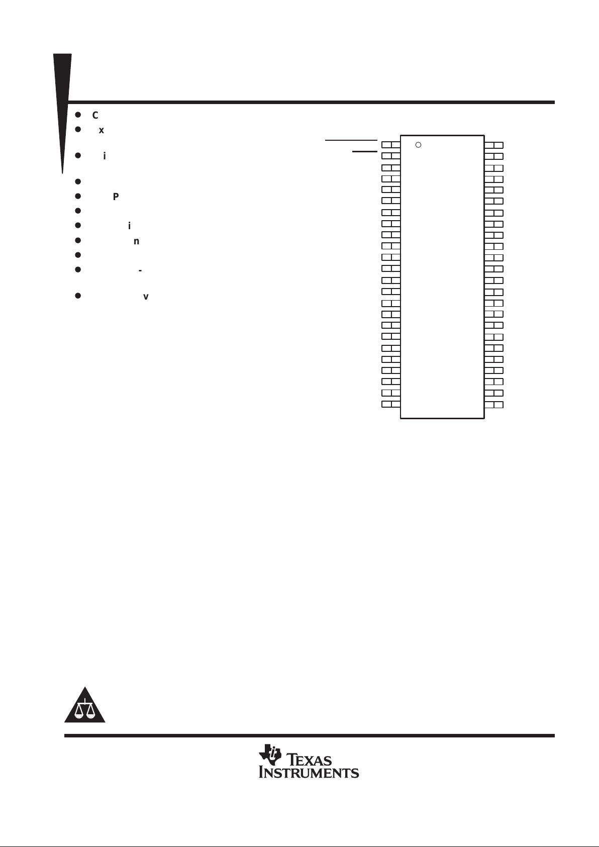
The TPA005D14 is offered in the thermally enhanced 48-pin PowerPAD TSSOP surface-mount package
(designator DCA).
Copyright 2000, Texas Instruments Incorporated
PRODUCTION DATA information is current as of publication date.
Products conform to specifications per the terms of Texas Instruments
standard warranty. Production processing does not necessarily include
testing of all parameters.
Please be aware that an important notice concerning availability, standard warranty, and use in critical applications of
Texas Instruments semiconductor products and disclaimers thereto appears at the end of this data sheet.
PowerPAD is a trademark of Texas Instruments Incorporated.
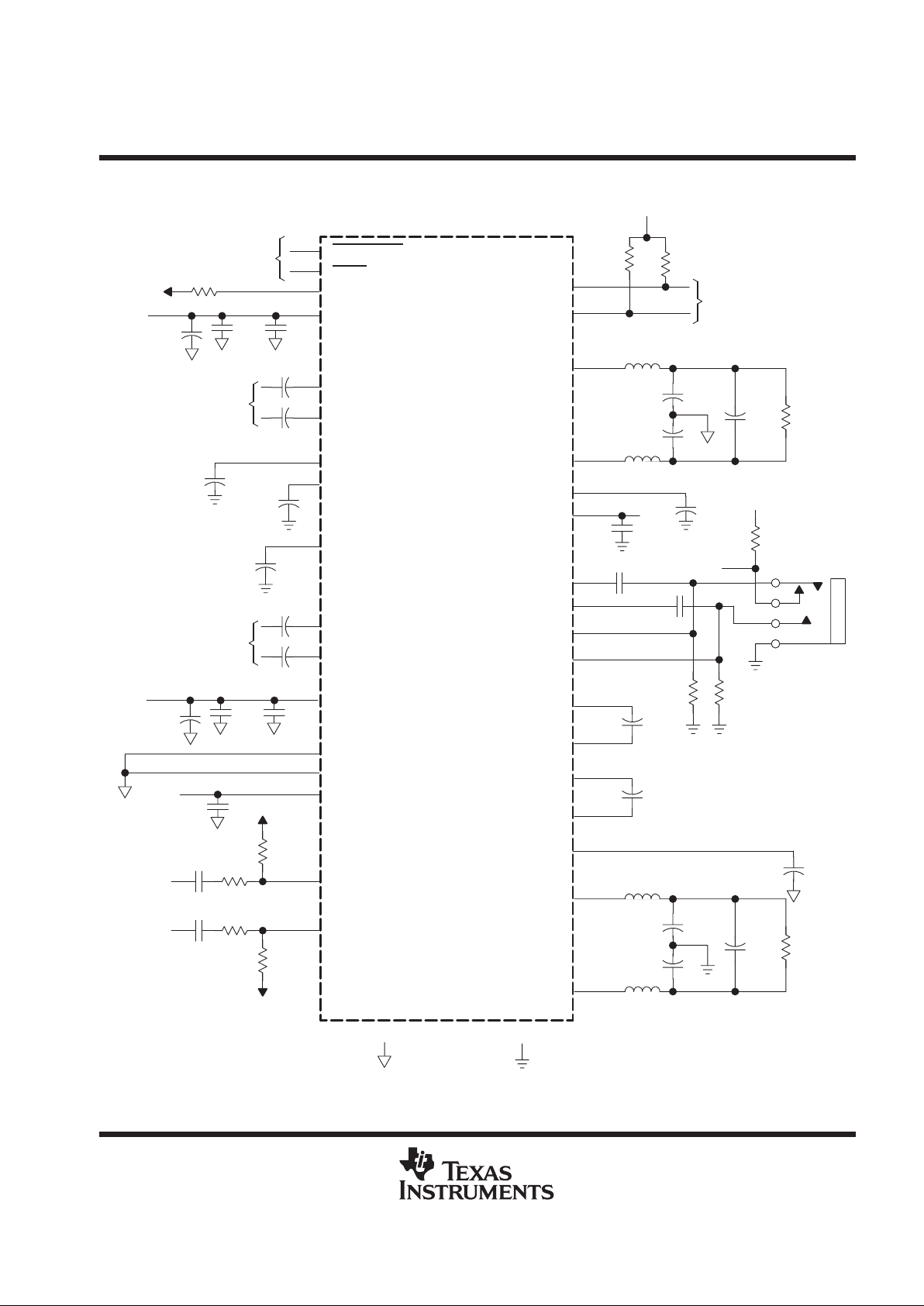
SHUTDOWN
MUTE
MODE
LINN
LINP
LCOMP
AGND
V
DD
LPV
DD
LOUTP
LOUTP
PGND
PGND
LOUTN
LOUTN
LPV
DD
HPDL
HPLOUT
HPLIN
AGND
PV
DD
VCP
CP3
CP2
COSC
AGND
AGND
RINN
RINP
RCOMP
FAULT0
FAULT1
RPV
DD
ROUTP
ROUTP
PGND
PGND
ROUTN
ROUTN
RPV
DD
HPDR
HPROUT
HPRIN
V2P5
PV
DD
PGND
CP4
CP1
1
2
3
4
5
6
7
8
9
10
11
12
13
14
15
16
17
18
19
20
21
22
23
24
48
47
46
45
44
43
42
41
40
39
38
37
36
35
34
33
32
31
30
29
28
27
26
25
DCA PACKAGE
(TOP VIEW)
TPA005D14
2-W STEREO CLASS-D AUDIO POWER AMPLIFIER
SLOS240A – AUGUST 1999 – REVISED MARCH 2000
Template Release Date: 7–11–94
2
POST OFFICE BOX 655303 DALLAS, TEXAS 75265
•
_
+
_
+
LINP
RAMP
GENERATOR
_
+
_
+
GATE
DRIVE
LPV
DD
GATE
DRIVE
LPV
DD
GATE
DRIVE
RPV
DD
GATE
DRIVE
RPV
DD
OVER-I
DETECT
THERMAL
DETECT
VCP-UVLO
DETECT
TRIPLER
CHARGE PUMP
_
+
_
+
CONTROL and
STARTUP
LOGIC
GENERATOR
PV
DD
PV
DD
LINN
LCOMP
COSC
RCOMP
RINP
RINN
RPV
DD
AGND
LPV
DD
ROUTP
ROUTN
PV
DD
VCP
CP4
CP3
CP2
CP1
LOUTP
LOUTN
FAULT0
FAULT1
SHUTDOWN
MODE
MUTE
V2P5
HPLIN
HPLOUT
HPROUT
HPRIN
LPV
DD
RPV
DD
PGND
VCP PV
DD
VCP PV
DD
VCP PV
DD
VCP PV
DD
V
DD
V
DD
PV
DD
10 kΩ10 kΩ
1.5 V
10 kΩ10 kΩ
1.5 V
HP
DEPOP
HPDL
HPDR
LPV
DD
RPV
DD
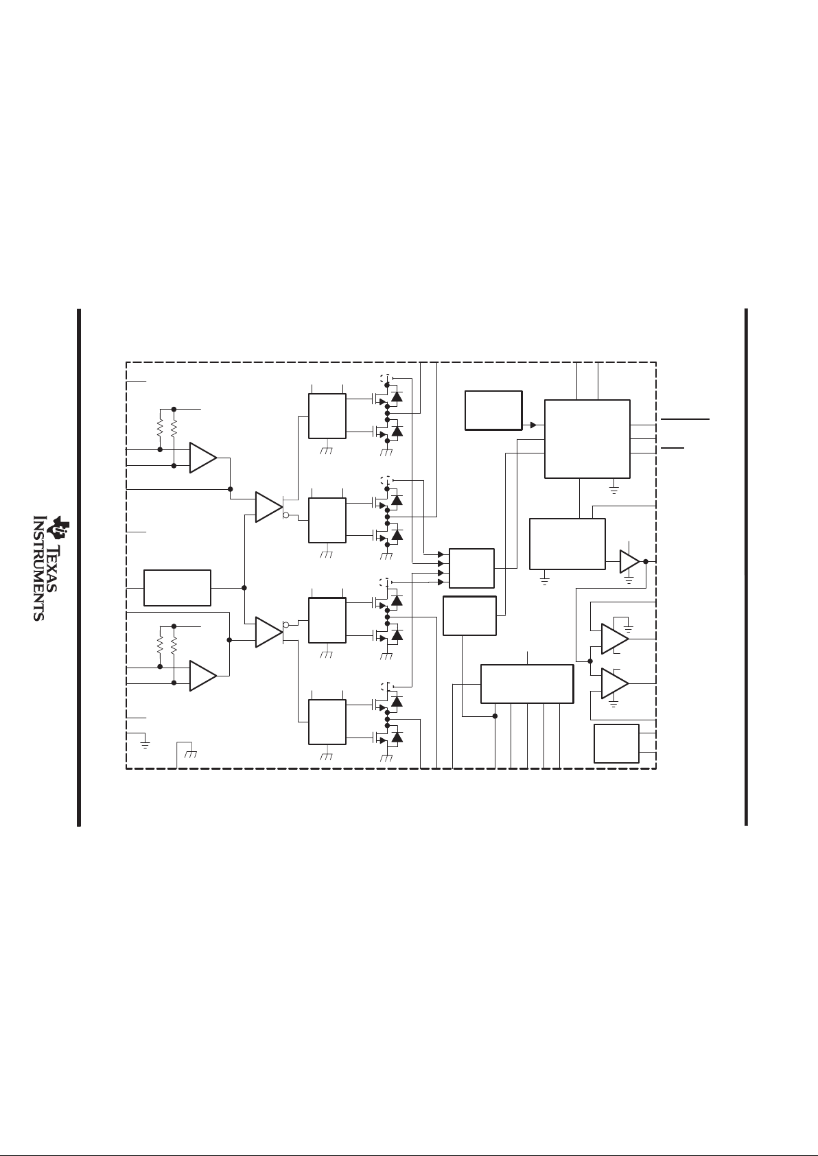
NOTE A: LPVDD, RPVDD, VDD, and PVDD are externally connected. AGND and PGND are externally connected.
schematic
TPA005D14
2-W STEREO CLASS-D AUDIO POWER AMPLIFIER
SLOS240A – AUGUST 1999 – REVISED MARCH 2000
3
POST OFFICE BOX 655303 • DALLAS, TEXAS 75265
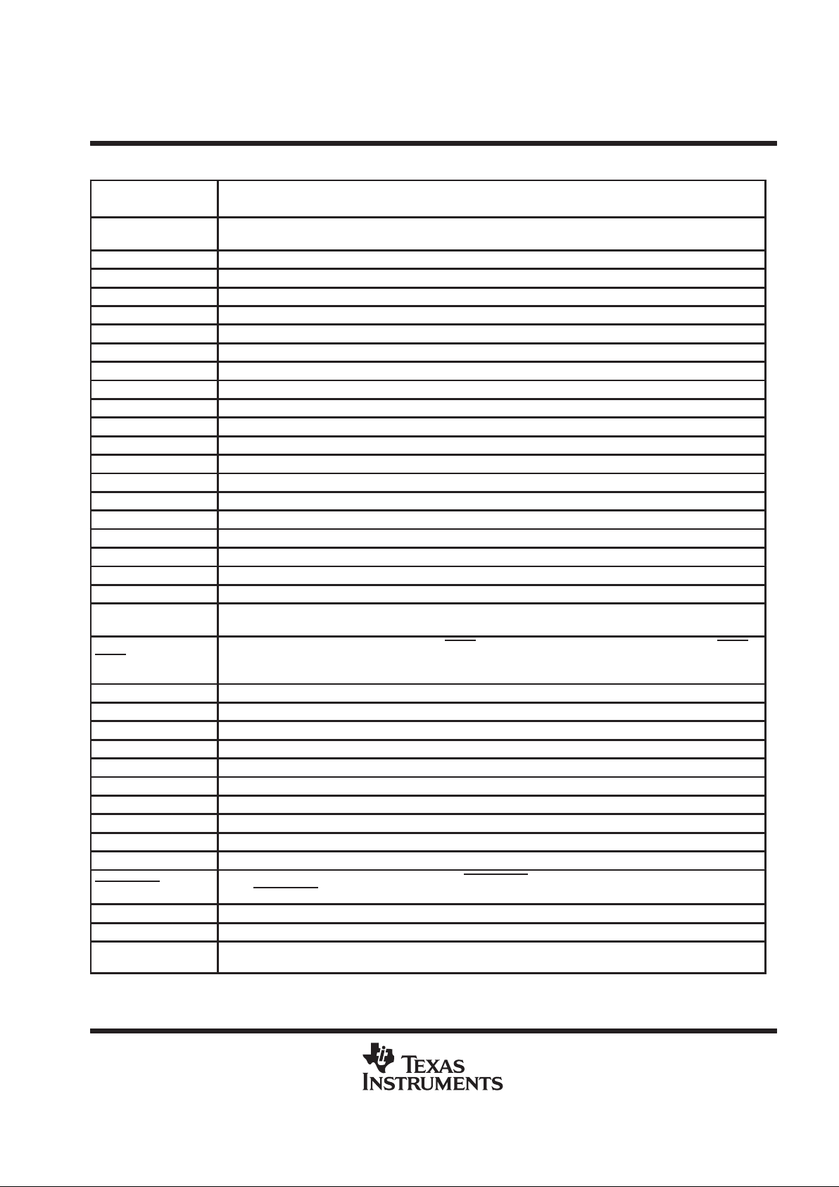
Terminal Functions
TERMINAL
NAME NO.
DESCRIPTION
AGND
7, 20,
46, 47
Analog ground for headphone and Class-D analog sections
COSC 48 Capacitor I/O for ramp generator. Adjust the capacitor size to change the switching frequency.
CP1 25 First diode node for charge pump
CP2 24 First inverter switching node for charge pump
CP3 23 Second diode node for charge pump
CP4 26 Second inverter switching node for charge pump
FAULT0 42 Logic level fault0 output signal. Lower order bit of the two fault signals with open drain output.
FAULT1 41 Logic level fault1 output signal. Higher order bit of the two fault signals with open drain output.
HPDL 17 Depop control for left headphone
HPDR 32 Depop control for right headphone
HPLIN 19 Headphone amplifier left input
HPLOUT 18 Headphone amplifier left output
HPRIN 30 Headphone amplifier right input
HPROUT 31 Headphone amplifier right output
LCOMP 6 Compensation capacitor terminal for left-channel Class-D amplifier
LINN 4 Class-D left-channel negative input
LINP 5 Class-D left-channel positive input
LOUTN 14, 15 Class-D amplifier left-channel negative output of H-bridge
LOUTP 10, 11 Class-D amplifier left-channel positive output of H-bridge
LPV
DD
9, 16 Class-D amplifier left-channel power supply
MODE 3
Logic-level mode input signal. When MODE is held low, the main Class-D amplifier is active. When MODE is held
high, the head phone amplifier is active.
MUTE
2
Active-low logic-level mute input signal. When MUTE is held low, the selected amplifier is muted. When MUTE is
held high, the device operates normally. When the Class-D amplifier is muted, the low-side output transistors are
turned on, shorting the load to ground.
PGND 12, 13 Power ground for left-channel H–bridge only
PGND 27 Power ground for charge pump only
PGND 36, 37 Power ground for right-channel H-bridge only
PV
DD
21, 28 VDD supply for charge-pump and gate-drive circuitry
RCOMP 43 Compensation capacitor terminal for right-channel Class-D amplifier
RINN 45 Class-D right-channel negative input
RINP 44 Class-D right-channel positive input
RPV
DD
33, 40 Class-D amplifier right-channel power supply
ROUTN 34, 35 Class-D amplifier right-channel negative output of H-bridge
ROUTP 38, 39 Class-D amplifier right-channel positive output of H-bridge
SHUTDOWN
1
Active-low logic-level shutdown input signal. When SHUTDOWN is held low, the device goes into shutdown mode.
When SHUTDOWN
is held at logic high, the device operates normally.
V2P5 29 2.5-V internal reference bypass
VCP 22 Storage capacitor terminal for charge pump
V
DD
8
VDD bias supply for analog circuitry. This terminal needs to be well filtered to prevent degrading the device
performance.
TPA005D14
2-W STEREO CLASS-D AUDIO POWER AMPLIFIER
SLOS240A – AUGUST 1999 – REVISED MARCH 2000
4
POST OFFICE BOX 655303 • DALLAS, TEXAS 75265
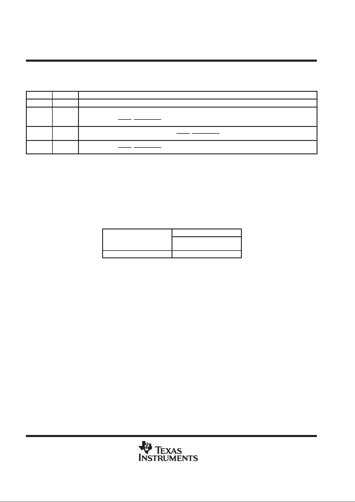
Class-D amplifier faults
Table 1. Class-D Amplifier Fault Table
FAULT 0†FAULT 1
†
DESCRIPTION
1 1 No fault. — The device is operating normally.
0 1 Charge pump under-voltage lock-out (VCP-UV) fault — All low-side transistors are turned on, shorting the load to
ground. Once the charge pump voltage is restored, normal operation resumes, but FAULT1 is still active. FAULT1 is
cleared by cycling MUTE
, SHUTDOWN, or the power supply.
1 0 Over-current fault — The output transistors are all switched off. This causes the load to be in a high-impedance state.
This is a latched fault and is cleared by cycling MUTE
, SHUTDOWN, or the power supply.
0 0 Thermal fault — All the low-side transistors are turned on, shorting the load to ground. This is latched fault and is
cleared by cycling MUTE
, SHUTDOWN, or the power supply.
†
These logic levels assume a pullup to PVDD from the open-drain outputs.
headphone amplifier faults
The thermal fault remains active when the device is in head phone mode. This fault operates exactly the same
as it does for the Class-D amplifier (see Table 1).
If LPVDD or RPV
DD
drops below 4.5 V , the headphone is disabled by the under-voltage lockout circuitry . Once
LPVDD and RPVDD exceed 4.5 V, the headphone amplifier is re-enabled. No fault is reported to the user.
AVAILABLE OPTIONS
PACKAGED DEVICES
T
A
TSSOP
†
(DCA)
–40°C to 125°C TPA005D14DCA
†
The DCA package is available in left-ended tape and reel. T o order
a taped and reeled part, add the suffix R to the part number (e.g.,
TPA005D14DCAR).
TPA005D14
2-W STEREO CLASS-D AUDIO POWER AMPLIFIER
SLOS240A – AUGUST 1999 – REVISED MARCH 2000
5
POST OFFICE BOX 655303 • DALLAS, TEXAS 75265
absolute maximum ratings over operating free-air temperature range, TC = 25°C (unless otherwise
noted)
‡
Supply voltage, VDD (PVDD, LPVDD, RPVDD, VDD) 5.5 V. . . . . . . . . . . . . . . . . . . . . . . . . . . . . . . . . . . . . . . . . . .
Input voltage, VI (SHUTDOWN, MUTE, MODE) –0.3 V to 5.8 V. . . . . . . . . . . . . . . . . . . . . . . . . . . . . . . . . . . . . . .
Output current, IO (FAULT0, FAULT1), open drain terminated 1 mA. . . . . . . . . . . . . . . . . . . . . . . . . . . . . . . . . . .
Charge pump voltage, VCP PVDD + 15 V. . . . . . . . . . . . . . . . . . . . . . . . . . . . . . . . . . . . . . . . . . . . . . . . . . . . . . . . . .
Continuous H-bridge output current 2 A. . . . . . . . . . . . . . . . . . . . . . . . . . . . . . . . . . . . . . . . . . . . . . . . . . . . . . . . . . .
Pulsed H-Bridge output current, each output, I
max
(see Note 1) 5 A. . . . . . . . . . . . . . . . . . . . . . . . . . . . . . . . . . .
Continuous total power dissipation See Dissipation Ratings Table. . . . . . . . . . . . . . . . . . . . . . . . . . . . . . . . . . . .
Operating virtual junction temperature range, TJ –40°C to 150°C. . . . . . . . . . . . . . . . . . . . . . . . . . . . . . . . . . . . .
Operating case temperature range, TC –40°C to 125°C. . . . . . . . . . . . . . . . . . . . . . . . . . . . . . . . . . . . . . . . . . . . .
Storage temperature range, T
stg
–40°C to 150°C. . . . . . . . . . . . . . . . . . . . . . . . . . . . . . . . . . . . . . . . . . . . . . . . . . .
Lead temperature 1,6 mm (1/16 inch) from case for 10 seconds 260°C. . . . . . . . . . . . . . . . . . . . . . . . . . . . . . .
†
Stresses beyond those listed under “absolute maximum ratings” may cause permanent damage to the device. These are stress ratings only, and
functional operation of the device at these or any other conditions beyond those indicated under “recommended operating conditions” is not
implied. Exposure to absolute-maximum-rated conditions for extended periods may affect device reliability.
NOTE 1: Pulse duration = 10 ms, duty cycle v 2%
DISSIPATION RATING TABLE
PACKAGE
TA ≤ 25°C
‡
POWER RATING
DERATING FACTOR
ABOVE TA = 25°C
TA = 70°C
POWER RATING
TA = 85°C
POWER RATING
TA = 125°C
POWER RATING
DCA 5.6 W 44.8 mW/°C 3.6 W 2.9 W 1.1 mW
‡
See the Texas Instruments document,
PowerPAD Thermally Enhanced Package Application Report
(literature number
SLMA002), for more information on the PowerP AD package. The thermal data was measured on a PCB layout based on the
information in the section entitled
T exas Instruments Recommended Board for PowerP AD
on page 33 of the before mentioned
document.
recommended operating conditions
MIN NOM MAX UNIT
Supply voltage, PVDD, LPVDD, RPVDD, V
DD
4.5 5.5 V
High-level input voltage, VIH (MUTE, MODE, SHUTDOWN) 4.25 V
Low-level input voltage, VIL (MUTE, MODE, SHUTDOWN) 0.75 V
Audio inputs, LINN, LINP, RINN, RINP, HPLIN, HPRIN, differential input voltage 1 V
RMS
PWM frequency 150 450 kHZ
electrical characteristics, Class-D amplifier, VDD = PVDD = LPVDD = RPVDD = 5 V, RL = 4 Ω,
T
A
= 25°C, See Figure 1 (unless otherwise noted)
PARAMETER TEST CONDITIONS MIN TYP MAX UNIT
Power supply rejection ratio VDD = PVDD = LPVDD = RPVDD = 4.5 V to 5.5 V –40 dB
I
DD
Supply current No output filter connected 25 35 mA
IDD(MUTE) Supply current, mute mode MUTE = 0 V 3.9 10 mA
IDD(SD) Supply current, shutdown mode SHUTDOWN = 0 V 0.2 10 µA
I
IH
High-level input current VIH = 5.3 V 1 µA
I
IL
Low-level input current VIL = –0.3 V –1 µA
r
DS(on)
Total static drain-to-source on-state
resistance (low-side plus high-side
FETs)
ID = 0.5 A 700 900 mΩ
r
DS(on)
Matching, high-side to high-side,
low-side to low-side, same channel
ID = 0.5 A 95% 98%
TPA005D14
2-W STEREO CLASS-D AUDIO POWER AMPLIFIER
SLOS240A – AUGUST 1999 – REVISED MARCH 2000
6
POST OFFICE BOX 655303 • DALLAS, TEXAS 75265
operating characteristics, Class-D amplifier, VDD = PVDD = LPVDD = RPVDD = 5 V, RL = 4 Ω,
T
A
= 25°C, See Figure 1 (unless otherwise noted)
PARAMETER TEST CONDITIONS MIN TYP MAX UNIT
P
O
RMS output power
f = 1 kHz, THD = 0.5%,
Per channel
2 W
THD+N Total harmonic distortion plus noise PO = 1 W, f = 1 kHz 0.2%
Efficiency PO = 1 W, RL = 8 Ω 80%
A
V
Gain 20 dB
Left/right channel gain matching 95% 99%
Noise floor –55 dBV
Dynamic range 70 dB
Crosstalk f = 1 kHz –55 dB
Frequency response bandwidth, post output filter, –3 dB 20 20000 Hz
B
OM
Maximum output power bandwidth 20 kHz
Z
I
Input impedance 10 kΩ
electrical characteristics, headphone amplifier, PVDD = LPVDD= RPVDD = 5 V , RL = 32 Ω, TA = 25°C,
See Figure 3 (unless otherwise noted)
PARAMETER TEST CONDITIONS MIN TYP MAX UNIT
Power supply rejection ratio PVDD = 4.5 V to 5.5 V,
AV = –1 V/V
–60 dB
Uncompensated gain range –1 –10 V/V
I
DD
Supply current 8 10 mA
IDD(MUTE) Supply current, mute mode 1.5 2 mA
IDD(SD) Supply current, shutdown mode 0.2 10 µA
I
IB
Input bias current 30 µA
operating characteristics, headphone amplifier, PVDD = LPVDD = RPVDD = 5 V , RL = 32 Ω, TA = 25°C,
See Figure 3 (unless otherwise noted)
PARAMETER TEST CONDITIONS MIN TYP MAX UNIT
P
O
Output power
THD = 0.5%, f = 1 kHz,
AV = –10V/V
50 mW
Supply voltage rejection ratio f = 1 kHz –60 dB
Noise floor –84 dBV
Dynamic range 90 dB
Crosstalk f = 1 kHz –38 dB
Frequency response bandwidth, post output filter, –3 dB 20 20000 Hz
B
OM
Maximum output power bandwidth 20 kHz
Z
I
Input impedance >1 MΩ
thermal shutdown
PARAMETER TEST CONDITIONS MIN TYP MAX UNIT
Thermal shutdown temperature 165 °C
TPA005D14
2-W STEREO CLASS-D AUDIO POWER AMPLIFIER
SLOS240A – AUGUST 1999 – REVISED MARCH 2000
7
POST OFFICE BOX 655303 • DALLAS, TEXAS 75265
PARAMETER MEASUREMENT INFORMATION
LINP
LINN
LCOMP
V
DD
COSC
RCOMP
RINP
RINN
RPV
DD
AGND (see Note A)
LPV
DD
PV
DD
SHUTDOWN
V2P5
HPLIN
HPLOUT
HPROUT
HPRIN
PGND (see Note A)
15 µH
15 µH
0.22 µF
0.22 µF
1 µF
4 Ω
5 V
5 V
1 µF
1 µF
Balanced
Differential
Input Signal
470 pF
470 pF
470 pF
1 µF
1 µF
Balanced
Differential
Input Signal
5 V
CP1
CP2
CP3
CP4
VCP
FAULT0
FAULT1
MODE
MUTE
PV
DD
PV
DD
1 µF
LOUTP
LOUTN
15 µH
15 µH
0.22 µF
0.22 µF
1 µF
4 Ω
ROUTP
ROUTN
47 nF
47 nF
0.1 µF
42
1
2
3
9,16
5
4
6
43
48
44
45
33,40
7,20,46,47
12,13,27,36,37
21, 28
19
30
41
14,15
10,11
29
8
18
31
25
24
23
26
22
34,35
38,39
HPDL
17
HPDR
32
Figure 1. 5-V, 4-Ω Test Circuit, Class-D Amplifier
TPA005D14
2-W STEREO CLASS-D AUDIO POWER AMPLIFIER
SLOS240A – AUGUST 1999 – REVISED MARCH 2000
8
POST OFFICE BOX 655303 • DALLAS, TEXAS 75265
PARAMETER MEASUREMENT INFORMATION
LINP
LINN
LCOMP
V
DD
COSC
RCOMP
RINP
RINN
RPV
DD
AGND
LPV
DD
PV
DD
SHUTDOWN
HPDR
V2P5
HPLIN
HPLOUT
HPROUT
HPRIN
PGND
5 V
5 V
470 pF
470 pF
470 pF
5 V
CP1
CP2
CP3
CP4
VCP
FAULT0
FAULT1
MODE
MUTE
1 µF
LOUTP
LOUTN
ROUTP
ROUTN
47 nF
0.1 µF
42
1
2
3
9,16
5
4
6
43
48
44
45
33,40
7,20,46,47
12,13,27,36,37
21, 28
19
30
41
14,15
10,11
29
8
18
31
32
25
24
23
26
22
34,35
38,39
5 V
5 V
5 V
Left SE
HP Input
HPLOUT
100 kΩ
100 kΩ
0.1 µF
Right SE
HP Input
100 kΩ
0.1 µF
100
kΩ
32 Ω
220 µF
220 µF
32 Ω
5 V
HPROUT
47 nF
HPDL
17
Figure 2. Headphone Test Circuit
TPA005D14
2-W STEREO CLASS-D AUDIO POWER AMPLIFIER
SLOS240A – AUGUST 1999 – REVISED MARCH 2000
9
POST OFFICE BOX 655303 • DALLAS, TEXAS 75265
PARAMETER MEASUREMENT INFORMATION
LINP
LINN
LCOMP
V
DD
COSC
RCOMP
RINP
RINN
RPV
DD
AGND
LPV
DD
PV
DD
SHUTDOWN
V2P5
HPLOUT
HPROUT
PGND
15 µH
15 µH
0.22 µF
0.22 µF
1 µF
4 Ω
5 V
5 V
1 µF
1 µF
Left Class-D Balanced
Differential Input
Signal
470 pF
470 pF
470 pF
1 µF
1 µF
HPDR
HPDL
CP1
CP2
VCP
FAULT0
FAULT1
MODE
MUTE
1 µF
LOUTP
LOUTN
15 µH
15 µH
0.22 µF
0.22 µF
1 µF
4 Ω
ROUTP
ROUTN
47 nF
0.1 µF
42
1
2
3
9,16
5
4
6
43
48
44
45
33,40
7,20,46,47
12,13,27,36,37
21, 28
41
14,15
10,11
29
8
18
31
32
17
25
24
22
34,35
38,39
5 V
HPLIN
HPRIN
19
30
Left SE
HP Input
HPLOUT
100 kΩ
100 kΩ
0.1 µF
Right SE
HP Input
100 kΩ
0.1 µF
100
kΩ
To System
Control
100 kΩ
1 µF1 µF
10 µF
Right Class-D Balanced
Differential Input
Signal
5 V
1 µF1 µF
10 µF
1 µF
100 kΩ
100 kΩ
To System
Control
1 µF
100 kΩ
5 V
MODE
1 kΩ1 kΩ
NOTE A: = power ground and = analog ground
HPROUT
220 µF
220 µF
5 V
CP3
CP4
47 nF
23
26
Figure 3. TPA032D04 Typical Configuration Application Circuit

TPA005D14
2-W STEREO CLASS-D AUDIO POWER AMPLIFIER
SLOS240A – AUGUST 1999 – REVISED MARCH 2000
10
POST OFFICE BOX 655303 • DALLAS, TEXAS 75265
TYPICAL CHARACTERISTICS
Table of Graphs
FIGURE
pp
vs Switching frequency 4
IDDSupply current
vs Free-air temperature 5, 6
THD+N Total harmonic distortion plus noise
vs Frequency
7, 9, 11
12, 14, 15
THD+N
Total harmonic distortion lus noise
vs Output power 8, 10, 13
Gain and phase vs Frequency 16, 17
Crosstalk vs Frequency 18
Power dissipation vs Output power 19
Efficiency vs Output power 20
Figure 4
f – Frequency – kHz
10
20
30
40
50
100 200 300 400 500
SUPPLY CURRENT
vs
SWITCHING FREQUENCY
I
DD
– Supply Current – mA
With Output Filter
Without Output Filter
Class-D Amplifier
Figure 5
10
20
30
40
50
–50 –25 0 25 50 75 100 125 150
I
DD
– Supply Current – mA
With Output Filter
Without Output Filter
SUPPLY CURRENT
vs
FREE–AIR TEMPERATURE
TA – Free–Air Temperature – °C
Class-D Amplifier

TPA005D14
2-W STEREO CLASS-D AUDIO POWER AMPLIFIER
SLOS240A – AUGUST 1999 – REVISED MARCH 2000
11
POST OFFICE BOX 655303 • DALLAS, TEXAS 75265
TYPICAL CHARACTERISTICS
Figure 6
5
5.5
6.0
6.5
7.0
7.5
8.0
8.5
9.0
9.5
10.0
–50 –25 0 25 50 75 100 125 150
I
DD
– Supply Current – mA
SUPPLY CURRENT
vs
FREE–AIR TEMPERATURE
TA – Free–Air Temperature – °C
Headphone Amplifier
Figure 7
TOTAL HARMONIC DISTORTION + NOISE
vs
FREQUENCY
Class-D Amplifier
VDD = 5 V
RL = 8 Ω
0.1
0.01
1
THD+N –Total Harmonic Distortion + Noise – %
f – Frequency – Hz
20 100 1k 10k 30k
100 mW
1 W
500 mW
Figure 8
TOTAL HARMONIC DISTORTION + NOISE
vs
OUTPUT POWER
0.1
0.02
2
THD+N –Total Harmonic Distortion + Noise – %
PO – Output Power – W
0.01 0.1 1 10
1
f = 20 kHz
f = 20 Hz
f = 1 kHz
Class-D Amplifier
VDD = 5 V
RL = 8 Ω
Figure 9
TOTAL HARMONIC DISTORTION + NOISE
vs
FREQUENCY
Class-D Amplifier
VDD = 5 V
RL = 4 Ω
0.1
0.01
1
THD+N –Total Harmonic Distortion + Noise – %
f – Frequency – Hz
20 100 1k 10k 30k
1 W
500 mW
2 W

TPA005D14
2-W STEREO CLASS-D AUDIO POWER AMPLIFIER
SLOS240A – AUGUST 1999 – REVISED MARCH 2000
12
POST OFFICE BOX 655303 • DALLAS, TEXAS 75265
TYPICAL CHARACTERISTICS
Figure 10
TOTAL HARMONIC DISTORTION + NOISE
vs
OUTPUT POWER
0.1
0.04
2
THD+N –Total Harmonic Distortion + Noise – %
PO – Output Power – W
0.01 0.1 1 10
1
Class-D Amplifier
VDD = 5 V
RL = 4 Ω
f = 20 kHz
f = 1 kHz
f = 20 Hz
Figure 11
TOTAL HARMONIC DISTORTION + NOISE
vs
FREQUENCY
0.1
0.006
1
THD+N –Total Harmonic Distortion + Noise – %
f – Frequency – Hz
20 100 1k 10k 20k
0.01
Headphone Amplifier
CI = 10 µF
RL = 32 Ω
CO = 470 µF
AV = 10
AV = 5
AV = 1
Figure 12
TOTAL HARMONIC DISTORTION + NOISE
vs
FREQUENCY
0.1
0.005
1
THD+N –Total Harmonic Distortion + Noise – %
f – Frequency – Hz
20 100 1k 10k 20
k
0.01
Headphone Amplifier
VO = 1 V
PO = 40 mW
AV = 1
CI = 10 µF
RI = RF = 10 kΩ
CO = 470 µF
Figure 13
TOTAL HARMONIC DISTORTION + NOISE
vs
OUTPUT POWER
0.1
0.005
1
THD+N –Total Harmonic Distortion + Noise – %
PO – Output Power – W
0.001 0.01 0.1 0.2
0.01
Headphone Amplifier
VDD = 5 V
AV = 1
CI = 10 µF
RI = RF = 10 kΩ
CO = 470 µF
f = 20 kHz
f = 1 kHz
f = 20 Hz

TPA005D14
2-W STEREO CLASS-D AUDIO POWER AMPLIFIER
SLOS240A – AUGUST 1999 – REVISED MARCH 2000
13
POST OFFICE BOX 655303 • DALLAS, TEXAS 75265
TYPICAL CHARACTERISTICS
Figure 14
0.1
0.004
1
THD+N –Total Harmonic Distortion + Noise – %
f – Frequency – Hz
20 100 1k 10k 20k
0.01
VO = 1 V
AV = 1
CI = 10 µF
RI = RF = 50 kΩ
CO = 470 µF
RL = 10 kΩ
HEADPHONE AMPLIFIER
TOTAL HARMONIC DISTORTION + NOISE
vs
FREQUENCY
Figure 15
0.1
0.004
1
THD+N –Total Harmonic Distortion + Noise – %
f – Frequency – Hz
20 100 1k 10k 20k
0.01
VO = 1 V
CI = 10 µF
RI = RF = 10 kΩ
CO = 470 µF
AV = 10
AV = 5
AV = 1
HEADPHONE AMPLIFIER
TOTAL HARMONIC DISTORTION + NOISE
vs
FREQUENCY
4
2
0
100
f – Frequency – Hz
5
3
1
1k 10k 30k
Gain – dBV
10
–60°
–90°
Phase – Degrees
VDD = 5 V
PO = 2 W
RL = 4 Ω
10
–30°
0°
30°
60°
90°
6
7
8
9
Gain
Phase
CLASS-D AMPLIFIER
GAIN and PHASE
vs
FREQUENCY
Figure 16

TPA005D14
2-W STEREO CLASS-D AUDIO POWER AMPLIFIER
SLOS240A – AUGUST 1999 – REVISED MARCH 2000
14
POST OFFICE BOX 655303 • DALLAS, TEXAS 75265
TYPICAL CHARACTERISTICS
–6
–8
–10
100
f – Frequency – Hz
–5
–7
–9
1k 10k 30k
Gain – dBV
3
–120°
–180°
Phase – Degrees
20
–60°
0°
60°
120°
180°
–4
–2
–3
2
1
0
–1
VDD = 5 V
PO = 40 mW
AV = 1
CI = 10 µF
RI = RF = 10 kΩ
CO = 470 µF
Gain
Phase
HEADPHONE AMPLIFIER
GAIN and PHASE
vs
FREQUENCY
Figure 17
Figure 18
Crosstalk – dB
f – Frequency – Hz
20 100 1k 10k 20k
–48
–60
–52
–56
–36
–40
–44
VDD = 5 V
PO = 2 W
RL = 4 Ω
CLASS-D AMPLIFIER
CROSSTALK
vs
FREQUENCY
Figure 19
0
0.5
1.0
1.5
2.0
2.5
3.0
0 0.5 1.0 1.5 2.0 2.5
POWER DISSIPATION
vs
OUTPUT POWER
PO – Output Power – W
Class-D Amplifier
Power Dissipation – W
RL = 4 Ω
RL = 8 Ω

TPA005D14
2-W STEREO CLASS-D AUDIO POWER AMPLIFIER
SLOS240A – AUGUST 1999 – REVISED MARCH 2000
15
POST OFFICE BOX 655303 • DALLAS, TEXAS 75265
TYPICAL CHARACTERISTICS
40
45
50
55
60
65
70
75
80
85
90
0 0.5 1.0 1.5 2.0 2.5
EFFICIENCY
vs
OUTPUT POWER
PO – Output Power – W
Class-D Amplifier
Efficiency – %
RL = 4 Ω
RL = 8 Ω
Figure 20

TPA005D14
2-W STEREO CLASS-D AUDIO POWER AMPLIFIER
SLOS240A – AUGUST 1999 – REVISED MARCH 2000
16
POST OFFICE BOX 655303 • DALLAS, TEXAS 75265
APPLICATION INFORMATION
input capacitor, C
I
In the typical application an input capacitor, CI, is required to allow the amplifier to bias the input signal to the
proper dc level for optimum operation. In this case, CI and RIN, the TPA005D14’s input resistance forms a
high-pass filter with the corner frequency determined in equation 1.
(1)
f
c(highpass)
+
1
2pZIC
I
–3 dB
f
c
ZI is nominally 10 kΩ
The value of CI is important to consider as it directly affects the bass (low frequency) performance of the circuit.
Consider the example where the specification calls for a flat bass response down to 40 Hz. Equation 1 is
reconfigured as equation 2.
(2)
C
I
+
1
2pZIf
c
In this example, CI is 0.40 µF so one would likely choose a value in the range of 0.47 µF to 1 µF . A low-leakage
tantalum or ceramic capacitor is the best choice for the input capacitors. When polarized capacitors are used,
the positive side of the capacitor should face the amplifier input as the dc level there is held at 1.5 V, which is
likely higher than the source dc level. Please note that it is important to confirm the capacitor polarity in the
application.
differential input
The TP A005D14 has differential inputs to minimize distortion at the input to the IC. Since these inputs nominally
sit at 1.5 V, dc-blocking capacitors are required on each of the four input terminals. If the signal source is
single-ended, optimal performance is achieved by treating the signal ground as a signal. In other words,
reference the signal ground at the signal source, and run a trace to the dc-blocking capacitor which should be
located physically close to the TP A005D14. If this is not feasible, it is still necessary to locally ground the unused
input terminal through a dc-blocking capacitor.
power supply decoupling, C
S
The TPA005D14 is a high-performance Class-D CMOS audio amplifier that requires adequate power supply
decoupling to ensure the output total harmonic distortion (THD) is as low as possible. Power supply decoupling
also prevents oscillations for long lead lengths between the amplifier and the speaker. The optimum decoupling
is achieved by using two capacitors of different types that target different types of noise on the power supply
leads. For higher frequency transients, spikes, or digital hash on the line, a good low equivalent-seriesresistance (ESR) ceramic capacitor, typically 0.1 µF placed as close as possible to the device’s various V
DD
leads works best. For filtering lower-frequency noise signals, a larger aluminum electrolytic capacitor of 10 µF
or greater placed near the audio power amplifier is recommended.
The TP A005D14 has several different power supply terminals. This was done to isolate the noise resulting from
high-current switching from the sensitive analog circuitry inside the IC.

TPA005D14
2-W STEREO CLASS-D AUDIO POWER AMPLIFIER
SLOS240A – AUGUST 1999 – REVISED MARCH 2000
17
POST OFFICE BOX 655303 • DALLAS, TEXAS 75265
APPLICATION INFORMATION
mute and shutdown modes
The TP A005D14 employs both a mute and a shutdown mode of operation designed to reduce supply current,
IDD, to the absolute minimum level during periods of nonuse for battery-power conservation. The SHUTDOWN
input terminal should be held high during normal operation when the amplifier is in use. Pulling SHUTDOWN
low causes the outputs to mute and the amplifier to enter a low-current state, IDD = 0.2 µA. Mute mode alone
reduces I
DD
to 10 mA.
using low-ESR capacitors
Low-ESR capacitors are recommended throughout this applications section. A real (as opposed to ideal)
capacitor can be modeled simply as a resistor in series with an ideal capacitor. The voltage drop across this
resistor minimizes the beneficial effects of the capacitor in the circuit. The lower the equivalent value of this
resistance the more the real capacitor behaves like an ideal capacitor.
output filter components
The output inductors are key elements in the performance of the class-D audio amplifier system. It is important
that these inductors have a high enough current rating and a relatively constant inductance over frequency and
temperature. The current rating should be higher than the expected maximum current to avoid magnetically
saturating the inductor. When saturation occurs, the inductor loses its functionality and looks like a short circuit
to the PWM signal, which increases the harmonic distortion considerably.
A shielded inductor may be required if the class-D amplifier is placed in an EMI sensitive system; however, the
switching frequency is low for EMI considerations and should not be an issue in most systems. The dc series
resistance of the inductor should be low to minimize losses due to power dissipation in the inductor, which
reduces the efficiency of the circuit.
Capacitors are important in attenuating the switching frequency and high frequency noise, and in supplying
some of the current to the load. It is best to use capacitors with low equivalent-series-resistance (ESR). A low
ESR means that less power is dissipated in the capacitor as it shunts the high-frequency signals. Placing these
capacitors in parallel also parallels their ESR, effectively reducing the overall ESR value. The voltage rating is
also important, and, as a rule of thumb, should be 2 to 3 times the maximum rms voltage expected to allow for
high peak voltages and transient spikes. These output filter capacitors should be stable over temperature since
large currents flow through them.
For 8-Ω loads, double the inductor value and halve the common-mode capacitors (i.e., 15 µH to 30 µH). For
more information, see application report SLOA023,
Reducing and Eliminating the Class-D Output Filter
and
application report SLOA031,
Design Considerations for Class-D Audio Power Amplifiers
.
TPA005D14
2-W STEREO CLASS-D AUDIO POWER AMPLIFIER
SLOS240A – AUGUST 1999 – REVISED MARCH 2000
18
POST OFFICE BOX 655303 • DALLAS, TEXAS 75265
APPLICATION INFORMATION
efficiency of class-D vs linear operation
Amplifier efficiency is defined as the ratio of output power delivered to the load to power drawn from the supply .
In the efficiency equation below, PL is power across the load and P
SUP
is the supply power.
Efficiency+h
+
P
L
P
SUP
A high-efficiency amplifier has a number of advantages over one with lower efficiency . One of these advantages
is a lower power requirement for a given output, which translates into less waste heat that must be removed
from the device, smaller power supply required, and increased battery life.
Audio power amplifier systems have traditionally used linear amplifiers, which are well known for being
inefficient. Class-D amplifiers were developed as a means to increase the efficiency of audio power amplifier
systems.
A linear amplifier is designed to act as a variable resistor network between the power supply and the load. The
transistors operate in their linear region and voltage that is dropped across the transistors (in their role as
variable resistors) is lost as heat, particularly in the output transistors.
The output transistors of a class-D amplifier switch from full OFF to full ON (saturated) and then back again,
spending very little time in the linear region in between. As a result, very little power is lost to heat because the
transistors are not operated in their linear region. If the transistors have a low ON resistance, little voltage is
dropped across them, further reducing losses. The ideal class-D amplifier is 100% efficient, which assumes that
both the ON resistance (r
DS(ON)
) and the switching times of the output transistors are zero.
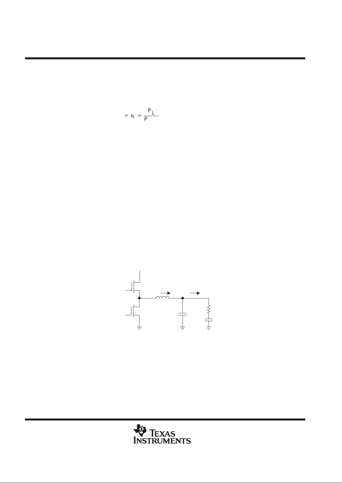
the ideal class-D amplifier
T o illustrate how the output transistors of a class-D amplifier operate, a half-bridge application is examined first
(Figure 21).
V
DD
V
OUT
L
C
L
R
L
I
L
I
OUT
+
–
V
A
M2
M1
C
Figure 21. Half-Bridge Class-D Output Stage
Figures 22 and 23 show the currents and voltages of the half-bridge circuit. When transistor M1 is on and M2
is off, the inductor current is approximately equal to the supply current. When M2 switches on and M1 switches
off, the supply current drops to zero, but the inductor keeps the inductor current from dropping. The additional
inductor current is flowing through M2 from ground. This means that V
A
(the voltage at the drain of M2, as shown
in Figure 21) transitions between the supply voltage and slightly below ground. The inductor and capacitor form
a low-pass filter, which makes the output current equal to the average of the inductor current. The low pass filter
averages V
A
, which makes V
OUT
equal to the supply voltage multiplied by the duty cycle.

TPA005D14
2-W STEREO CLASS-D AUDIO POWER AMPLIFIER
SLOS240A – AUGUST 1999 – REVISED MARCH 2000
19
POST OFFICE BOX 655303 • DALLAS, TEXAS 75265
APPLICATION INFORMATION
the ideal class-D amplifier (continued)
Control logic is used to adjust the output power, and both transistors are never on at the same time. If the output
voltage is rising, M1 is on for a longer period of time than M2.
Supply Current
Time
M1 on
M2 off
M1 off
M2 on
M1 on
M2 off
Output Current
Inductor Current
0
Current
Figure 22. Class-D Currents
V
DD
V
A
V
OUT
0
Voltage
Time
M1 on
M2 off
M1 off
M2 on
M1 on
M2 off
Figure 23. Class-D Voltages

TPA005D14
2-W STEREO CLASS-D AUDIO POWER AMPLIFIER
SLOS240A – AUGUST 1999 – REVISED MARCH 2000
20
POST OFFICE BOX 655303 • DALLAS, TEXAS 75265
APPLICATION INFORMATION
the ideal class-D amplifier (continued)
Given these plots, the efficiency of the class-D device can be calculated and compared to an ideal linear
amplifier device. In the derivation below, a sine wave of peak voltage (VP) is the output from an ideal class-D
and linear amplifier and the efficiency is calculated.
V
L(rms)
+
V
P
2
Ǹ
CLASS-D LINEAR
V
L(rms)
+
V
P
2
Ǹ
PL+
VL
I
L
AverageǒI
DD
Ǔ
+
I
L(rms)
V
L(rms)
V
DD
PL+
V
L(rms)
2
R
L
+
V
P
2
2R
L
AverageǒI
DD
Ǔ
+
2
p
V
P
R
L
P
SUP
+
VDD
AverageǒI
DD
Ǔ
P
SUP
+
VDD
AverageǒI
DD
Ǔ
+
VDDV
P
R
L
2
p
P
SUP
+
V
DD
I
L(rms)
V
L(rms)
V
DD
Efficiency+h
+
P
L
P
SUP
Efficiency+h
+
P
L
P
SUP
Efficiency+h+VDD
V
P
2
2R
L
2
p
V
P
R
L
Efficiency+h+1 Efficiency+h
+
p
4
V
P
V
DD
In the ideal efficiency equations, assume that VP = VDD, which is the maximum sine wave magnitude without
clipping. Then, the highest efficiency that a linear amplifier can have without clipping is 78.5%. A class-D
amplifier, however, can ideally have an efficiency of 100% at all power levels.
The derivation above applies to an H-bridge as well as a half-bridge. An H-bridge requires approximately twice
the supply current but only requires half the supply voltage to achieve the same output power—factors that
cancel in the efficiency calculation. The H-bridge circuit is shown in Figure 24.
V
DD
V
OUT
L
C
L
R
L
I
L
I
OUT
+
–
V
A
M2
M1
V
DD
L
C
L
M4
M3
Figure 24. H-Bridge Class-D Output Stage

TPA005D14
2-W STEREO CLASS-D AUDIO POWER AMPLIFIER
SLOS240A – AUGUST 1999 – REVISED MARCH 2000
21
POST OFFICE BOX 655303 • DALLAS, TEXAS 75265
APPLICATION INFORMATION
losses in a real-world class-D amplifier
Losses make class-D amplifiers nonideal, and reduce the efficiency below 100%. These losses are due to the
output transistors having a nonzero r
DS(on)
, and rise and fall times that are greater than zero.
The loss due to a nonzero r
DS(on)
is called conduction loss, and is the power lost in the output transistors at
nonswitching times, when the transistor is ON (saturated). Any R
DS(on)
above 0 Ω causes conduction loss.
Figure 25 shows an H-bridge output circuit simplified for conduction loss analysis and can be used to determine
new efficiencies with conduction losses included.
VDD = 5 V
R
L
4 Ω
0.35 Ω
0.35 Ω
R
DS(on)
R
DS(off)
R
DS(off)
R
DS(on)
5 MΩ
5 MΩ
Figure 25. Output Transistor Simplification for Conduction Loss Calculation
The power supplied, P
SUP
, is determined to be the power output to the load plus the power lost in the transistors,
assuming that there are always two transistors on.
Efficiency+h
+
I2R
L
I22r
DS(on)
)
I2R
L
Efficiency+h
+
P
L
P
SUP
Efficiency+h
+
R
L
2r
DS(on)
)
R
L
Efficiency+h+95%ǒat all output levels r
DS(on)
+
0.1, RL+
4
Ǔ
Efficiency+h+85%ǒat all output levels r
DS(on)
+
0.35, RL+
4
Ǔ

TPA005D14
2-W STEREO CLASS-D AUDIO POWER AMPLIFIER
SLOS240A – AUGUST 1999 – REVISED MARCH 2000
22
POST OFFICE BOX 655303 • DALLAS, TEXAS 75265
APPLICATION INFORMATION
losses in a real-world class-D amplifier (continued)
Losses due to rise and fall times are called switching losses. A plot of the output, showing switching losses, is
shown in Figure 26.
t
SWon
+
t
SWoff
=
t
SW
1
f
SW
Figure 26. Output Switching Losses
Rise and fall times are greater than zero for several reasons. One is that the output transistors cannot switch
instantaneously because (assuming a MOSFET) the channel from drain to source requires a specific period
of time to form. Another is that transistor gate-source capacitance and parasitic resistance in traces form RC
time constants that also increase rise and fall times.
Switching losses are constant at all output power levels, which means that switching losses can be ignored at
high power levels in most cases. At low power levels, however, switching losses must be taken into account
when calculating efficiency. Switching losses are dominated by conduction losses at the high output powers,
but should be considered at low powers. The switching losses are automatically taken into account if you
consider the quiescent current with the output filter and load.
class-D effect on power supply
Efficiency calculations are an important factor for proper power supply design in amplifier systems. Table 2
shows class-D efficiency at a range of output power levels (per channel) with a 1-kHz sine wave input. The
maximum power supply draw from a stereo 1-W per channel audio system with 8-Ω loads and a 5-V supply is
almost 2.7 W. A similar linear amplifier such as the TP A005D14 has a maximum draw of 3.25 W under the same
circumstances.
Table 2. Efficiency vs Output Power in 5-V 8-Ω H-Bridge Systems
Output Power (W) Efficiency (%) Peak Voltage (V) Internal Dissipation (W)
0.25 63.4 2 0.145
0.5 73 2.83 0.183
0.75 77.1 3.46 0.222
1 79.3 4 0.314
1.25 80.6 4.47
†
0.3
†
High peak voltages cause the THD to increase

TPA005D14
2-W STEREO CLASS-D AUDIO POWER AMPLIFIER
SLOS240A – AUGUST 1999 – REVISED MARCH 2000
23
POST OFFICE BOX 655303 • DALLAS, TEXAS 75265
APPLICATION INFORMATION
class-D effect on power supply (continued)
There is a minor power supply savings with a class-D amplifier versus a linear amplifier when amplifying sine
waves. The difference is much larger when the amplifier is used strictly for music. This is because music has
much lower RMS output power levels, given the same peak output power (Figure 27); and although linear
devices are relatively efficient at high RMS output levels, they are very inefficient at mid-to-low RMS power
levels. The standard method of comparing the peak power to RMS power for a given signal is crest factor, whose
equation is shown below. The lower RMS power for a set peak power results in a higher crest factor
Crest Factor
+
10 log
P
PK
P
rms
Time
P
PK
Power
P
RMS
Figure 27. Audio Signal Showing Peak and RMS Power
Figure 28 is a comparison of a 5-V class-D amplifier to a similar linear amplifier playing music that has a 13.76-dB
crest factor. From the plot, the power supply draw from a stereo amplifier that is playing music with a 13.76 dB
crest factor is 1.02 W, while a class-D amplifier draws 420 mW under the same conditions. This means that just
under 2.5 times the power supply is required for a linear amplifier over a class-D amplifier.
600
500
300
200
100
0
400
1 1.5 2 2.5
Power Supplied (mW)
POWER SUPPLIED
vs
PEAK OUTPUT VOLTAGE AND PEAK OUTPUT POWER
4 4.53
3.5
0.25 0.56 1 1.56 4 5.062.25
3.06
Peak Output Voltage (V)
Peak Output Power (W)
TPA0202
TPA005D14
Figure 28. Audio Signal Showing Peak and RMS Power (With Music Applied)

TPA005D14
2-W STEREO CLASS-D AUDIO POWER AMPLIFIER
SLOS240A – AUGUST 1999 – REVISED MARCH 2000
24
POST OFFICE BOX 655303 • DALLAS, TEXAS 75265
APPLICATION INFORMATION
class-D effect on battery life
Battery operations for class-D amplifiers versus linear amplifiers have similar power supply savings results. The
essential contributing factor to longer battery life is lower RMS supply current. Figure 29 compares the
TPA005D14 supply current to the supply current of the TPA0202, a 2-W linear device, while playing music at
different peak voltage levels.
400
350
250
200
150
0
300
1 1.5 2 2.5
Supply Current (mA rms)
SUPPLY CURRENTS
vs
PEAK OUTPUT VOLTAGE AND PEAK OUTPUT POWER
43
3.5
100
50
0.25 0.56 1 1.56 42.25
3.06
Peak Output Voltage (V)
Peak Output Power (W)
TPA0202
TPA005D14
Figure 29. Supply Current vs Peak Output Voltage of TPA005D14 vs TPA0202 With Music Input
This plot shows that a linear amplifier has approximately three times more current draw at normal listening levels
than a class-D amplifier. Thus, a class-D amplifier has approximately three times longer battery life at normal
listening levels. If there is other circuitry in the system drawing supply current, that must also be taken into
account when estimating battery life savings.

TPA005D14
2-W STEREO CLASS-D AUDIO POWER AMPLIFIER
SLOS240A – AUGUST 1999 – REVISED MARCH 2000
25
POST OFFICE BOX 655303 • DALLAS, TEXAS 75265
APPLICATION INFORMATION
crest factor and thermal considerations
A typical music CD requires 12 dB to 15 dB of dynamic headroom to pass the loudest portions without distortion
as compared with the average power output. From the TPA005D14 data sheet, one can see that when the
TP A005D14 is operating from a 5-V supply into a 4-Ω speaker that 4 W peaks are available. Converting W atts
to dB:
PdB+
10Log
ǒ
P
W
P
ref
Ǔ
+
10Log
ǒ
4
1
Ǔ
+
6dB
(3)
Subtracting the crest factor restriction to obtain the average listening level without distortion yields:
6.0 dB*15 dB
+*
9dB(15 dB crest factor
)
6.0 dB*12 dB
+*
6dB(12 dB crest factor
)
6.0 dB*9dB
+*
3dB(9 dB crest factor
)
6.0 dB*6dB
+*
0dB(6 dB crest factor
)
6.0 dB*3dB+3dB(3 dB crest factor
)
6.0 dB*18 dB
+*
12 dB(15 dB crest factor
)
Converting dB back into watts:
PW+
10
PdBń10
P
ref
+
125 mW (15 dB crest factor)
+
250 mW (12 dB crest factor)
+
500 mW (9 dB crest factor)
+
1000 mW (6 dB crest factor)
+
2000 mW (3 dB crest factor)
(4)
+
63 mW (18 dB crest factor)
This is valuable information to consider when attempting to estimate the heat dissipation requirements for the
amplifier system. Comparing the absolute worst case, which is 2 W of continuous power output with a 3 dB crest
factor, against 12 dB and 15 dB applications drastically af fects maximum ambient temperature ratings for the
system. Using the power dissipation curves for a 5-V, 4-Ω system, the internal dissipation in the TPA005D14
and maximum ambient temperatures is shown in Table 3.

TPA005D14
2-W STEREO CLASS-D AUDIO POWER AMPLIFIER
SLOS240A – AUGUST 1999 – REVISED MARCH 2000
26
POST OFFICE BOX 655303 • DALLAS, TEXAS 75265
APPLICATION INFORMATION
crest factor and thermal considerations (continued)
Table 3. TPA005D14 Power Rating, 5-V, 4-Ω, Stereo
PEAK OUTPUT POWER AVERAGE OUTPUT POWER DISSIPA TION MAXIMUM AMBIENT
(W) POWER (W/Channel) TEMPERATURE
4 2 W (3 dB) 0.56 125°C
4 1000 mW (6 dB) 0.30 136°C
†
4 500 mW (9 dB) 0.23 139°C
†
4 250 mW (12 dB) 0.20 141°C
†
4 120 mW (15 dB) 0.14 143°C
†
4 63 mW (18 dB) 0.09 146°C
†
†
Case temperature (TC) is rated to 125°C maximum.
DISSIPATION RATING TABLE
PACKAGE
TA ≤ 25°C
DERATING FACTOR TA = 70°C TA = 85°C
DCA
5.6 W
44.8 mW/°C
3.5 W
2.9 W
The maximum ambient temperature depends on the heatsinking ability of the PCB system. Using the 0 CFM
data from the dissipation rating table, the derating factor for the DCA package with 6.9 in2 of copper area on
a multilayer PCB is 44.8 mW/°C. Converting this to ΘJA:
Θ
JA
+
1
Derating
+
1
0.0448
+
22.3°CńW
(5)
To calculate maximum ambient temperatures, first consider that the numbers from the dissipation graphs are
per channel so the dissipated heat needs to be doubled for two channel operation. Given ΘJA, the maximum
allowable junction temperature, and the total internal dissipation, the maximum ambient temperature can be
calculated with the following equation. The maximum recommended junction temperature for the TP A005D14
is 150 °C. The internal dissipation figures are taken from the Efficiency vs Output Power graphs.
T
A
Max+TJMax
*
Θ
JAPD
+
150*22.3(0.14 2)+
143°C(15 dB crest factor
)
+
150*22.3(0.56 2)+
125°C(3dB crest factor
)
(6)
NOTE:
Internal dissipation of 0.6 W is estimated for a 2-W system with a 15 dB crest factor per channel.
Table 3 shows that for some applications no airflow is required to keep junction temperatures in the specified
range. The TPA005D14 is designed with thermal protection that turns the device off when the junction
temperature surpasses 150°C to prevent damage to the IC. Table 3 was calculated for maximum listening
volume without distortion. When the output level is reduced the numbers in the table change significantly . Also,
using 8-Ω speakers dramatically increases the thermal performance by increasing amplifier efficiency.

TPA005D14
2-W STEREO CLASS-D AUDIO POWER AMPLIFIER
SLOS240A – AUGUST 1999 – REVISED MARCH 2000
27
POST OFFICE BOX 655303 • DALLAS, TEXAS 75265
THERMAL INFORMATION
The thermally enhanced DCA package is based on the 56-pin TSSOP, but includes a thermal pad (see Figure 30)
to provide an effective thermal contact between the IC and the PWB.
Traditionally, surface mount and power have been mutually exclusive terms. A variety of scaled-down TO-220-type
packages have leads formed as gull wings to make them applicable for surface-mount applications. These packages,
however, have only two shortcomings: they do not address the very low profile requirements (<2 mm) of many of
today’s advanced systems, and they do not offer a terminal-count high enough to accommodate increasing
integration. On the other hand, traditional low-power surface-mount packages require power-dissipation derating that
severely limits the usable range of many high-performance analog circuits.
The PowerP AD package (thermally enhanced TSSOP) combines fine-pitch surface-mount technology with thermal
performance comparable to much larger power packages.
The PowerPAD package is designed to optimize the heat transfer to the PWB. Because of the very small size and
limited mass of a TSSOP package, thermal enhancement is achieved by improving the thermal conduction paths that
remove heat from the component. The thermal pad is formed using a patented lead-frame design and manufacturing
technique to provide a direct connection to the heat-generating IC. When this pad is soldered or otherwise thermally
coupled to an external heat dissipator, high power dissipation in the ultra-thin, fine-pitch, surface-mount package can
be reliably achieved.
DIE
Side View (a)
End View (b)
Bottom View (c)
DIE
Thermal
Pad
Figure 30. Views of Thermally Enhanced DCA Package

TPA005D14
2-W STEREO CLASS-D AUDIO POWER AMPLIFIER
SLOS240A – AUGUST 1999 – REVISED MARCH 2000
28
POST OFFICE BOX 655303 • DALLAS, TEXAS 75265
MECHANICAL DATA
DCA (R-PDSO-G**) PowerPAD PLASTIC SMALL-OUTLINE P ACKAGE
0,25
0,50
0,75
0,15 NOM
Gage Plane
6,00
6,20
8,30
7,90
Thermal Pad
(See Note D)
64
17,10
56
14,10
Seating Plane
16,9013,90
4073259/A 01/98
0,27
25
24
A
0,17
48 PINS SHOWN
48
1
48
DIM
PINS **
A MAX
A MIN
1,20 MAX
12,40
12,60
0,50
0,10
M
0,08
0°–8°
0,05
0,15
NOTES: A. All linear dimensions are in millimeters.
B. This drawing is subject to change without notice.
C. Body dimensions do not include mold flash or protrusion not to exceed 0,15.
D. The package thermal performance may be enhanced by bonding the thermal pad to an external thermal plane.
This pad is electrically and thermally connected to the backside of the die and possibly selected leads.
E. Falls within JEDEC MO-153
PowerPAD is a trademark of Texas Instruments.

IMPORTANT NOTICE
T exas Instruments and its subsidiaries (TI) reserve the right to make changes to their products or to discontinue
any product or service without notice, and advise customers to obtain the latest version of relevant information
to verify, before placing orders, that information being relied on is current and complete. All products are sold
subject to the terms and conditions of sale supplied at the time of order acknowledgment, including those
pertaining to warranty, patent infringement, and limitation of liability.
TI warrants performance of its semiconductor products to the specifications applicable at the time of sale in
accordance with TI’s standard warranty. Testing and other quality control techniques are utilized to the extent
TI deems necessary to support this warranty. Specific testing of all parameters of each device is not necessarily
performed, except those mandated by government requirements.
Customers are responsible for their applications using TI components.
In order to minimize risks associated with the customer’s applications, adequate design and operating
safeguards must be provided by the customer to minimize inherent or procedural hazards.
TI assumes no liability for applications assistance or customer product design. TI does not warrant or represent
that any license, either express or implied, is granted under any patent right, copyright, mask work right, or other
intellectual property right of TI covering or relating to any combination, machine, or process in which such
semiconductor products or services might be or are used. TI’s publication of information regarding any third
party’s products or services does not constitute TI’s approval, warranty or endorsement thereof.
Copyright 2000, Texas Instruments Incorporated
 Loading...