

Page 1
TPA005D12
2-W STEREO CLASS-D AUDIO POWER AMPLIFIER
SLOS241B – AUGUST 1999 – REVISED MARCH 2000
1
POST OFFICE BOX 655303 • DALLAS, TEXAS 75265
NOT RECOMMENDED FOR NEW DESIGNS
D
Choose TPA2000D2 For Upgrade
D
Extremely Efficient Class-D Stereo
Operation
D
Drives L and R Channels
D
2-W BTL Output Into 4 Ω
D
5-W Peak Music Power
D
Fully Specified for 5-V Operation
D
Low Quiescent Current
D
Shutdown Control . . . 0.2 µA
D
Thermally-Enhanced PowerP AD SurfaceMount Packaging
D
Thermal, Over-Current, and Under-V oltage
Protection
description
The TPA005D12 is a monolithic power IC stereo
audio amplifier that operates in extremely efficient
Class-D operation, using the high switching speed
of power DMOS transistors to replicate the analog
input signal through high-frequency switching of
the output stage. This allows the TPA005D12 to
be configured as a bridge-tied load (BTL) amplifier
capable of delivering up to 2 W of continuous
average power into a 4-Ω load at 0.5% THD+N
from a 5-V power supply in the high-fidelity audio
frequency range (20 Hz to 20 kHz). A BTL configuration eliminates the need for external coupling capacitors
on the output. A chip-level shutdown control is provided to limit total quiescent current to 0.2 µA, making the
device ideal for battery-powered applications.
A full range of protection circuitry is included to increase device reliability: thermal, over-current, and
under-voltage shutdown, with two status feedback terminals for use when any error condition is encountered.
The high switching frequency of the TP A005D12 allows the output filter to consist of three small capacitors and
two small inductors per channel. The high switching frequency also allows for good THD+N performance.
The TPA005D12 is offered in the thermally enhanced 48-pin PowerPAD TSSOP surface-mount package
(designator DCA).
AVAILABLE OPTIONS
PACKAGED DEVICES
T
A
TSSOP
†
(DCA)
–40°C to 125°C TPA005D12DCA
†
The DCA package is available in left-ended tape and reel. T o order
a taped and reeled part, add the suffix R to the part number (e.g.,
TPA005D12DCAR).
Copyright 2000, Texas Instruments Incorporated
PRODUCTION DATA information is current as of publication date.
Products conform to specifications per the terms of Texas Instruments
standard warranty. Production processing does not necessarily include
testing of all parameters.
Please be aware that an important notice concerning availability, standard warranty, and use in critical applications of
Texas Instruments semiconductor products and disclaimers thereto appears at the end of this data sheet.
PowerPAD is a trademark of Texas Instruments Incorporated.
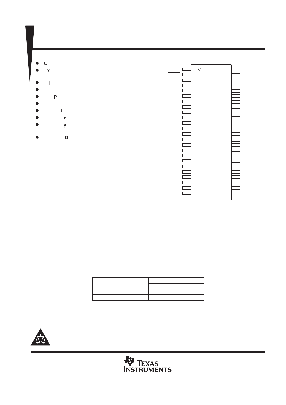
SHUTDOWN
MUTE
AGND
LINN
LINP
LCOMP
AGND
V
DD
LPV
DD
LOUTP
LOUTP
PGND
PGND
LOUTN
LOUTN
LPV
DD
NC
NC
NC
AGND
PV
DD
VCP
CP3
CP2
COSC
AGND
AGND
RINN
RINP
RCOMP
FAULT0
FAULT1
RPV
DD
ROUTP
ROUTP
PGND
PGND
ROUTN
ROUTN
RPV
DD
NC
NC
NC
V2P5
PV
DD
PGND
CP4
CP1
NC – No internal connection
1
2
3
4
5
6
7
8
9
10
11
12
13
14
15
16
17
18
19
20
21
22
23
24
48
47
46
45
44
43
42
41
40
39
38
37
36
35
34
33
32
31
30
29
28
27
26
25
DCA PACKAGE
(TOP VIEW)
Page 2
TPA005D12
2-W STEREO CLASS-D AUDIO POWER AMPLIFIER
SLOS241B – AUGUST 1999 – REVISED MARCH 2000
Template Release Date: 7–11–94
2
POST OFFICE BOX 655303 DALLAS, TEXAS 75265
•
_
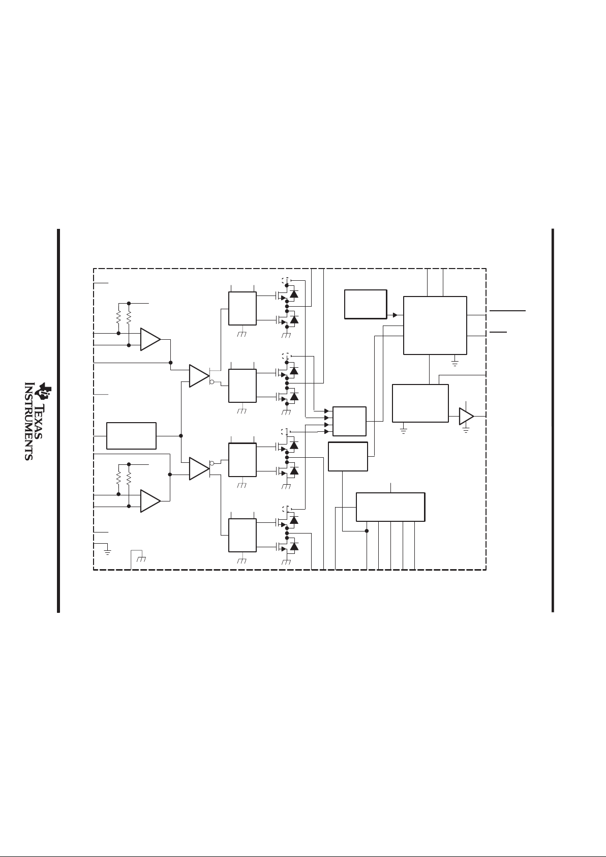
+
_
+
LINP
RAMP
GENERATOR
_
+
_
+
GATE
DRIVE
LPV
DD
GATE
DRIVE
LPV
DD
GATE
DRIVE
RPV
DD
GATE
DRIVE
RPV
DD
OVER-I
DETECT
THERMAL
DETECT
VCP-UVLO
DETECT
TRIPLER
CHARGE PUMP
CONTROL and
STARTUP
LOGIC
GENERATOR
PV
CC
PV
DD
LINN
LCOMP
COSC
RCOMP
RINP
RINN
RPV
DD
AGND
LPV
DD
ROUTP
ROUTN
PV
DD
VCP
CP4
CP3
CP2
CP1
LOUTP
LOUTN
FAULT0
FAULT1
SHUTDOWN
MUTE
V2P5
LPV
DD
RPV
DD
PGND
VCP PV
DD
VCP PV
DD
VCP PV
DD
VCP PV
DD
V
DD
V
DD
PV
DD
10 kΩ10 kΩ
1.5 V
10 kΩ10 kΩ
1.5 V
NOTE A: LPVDD, RPVDD, VDD, and PVDD are externally connected. AGND and PGND are externally connected.
schematic
Page 3
TPA005D12
2-W STEREO CLASS-D AUDIO POWER AMPLIFIER
SLOS241B – AUGUST 1999 – REVISED MARCH 2000
3
POST OFFICE BOX 655303 • DALLAS, TEXAS 75265
Terminal Functions
TERMINAL
NAME NO.
DESCRIPTION
AGND
3, 7, 20,
46, 47
Analog ground for headphone and Class-D analog sections
COSC 48 Capacitor I/O for ramp generator. Adjust the capacitor size to change the switching frequency.
CP1 25 First diode node for charge pump
CP2 24 First inverter switching node for charge pump
CP3 23 Second diode node for charge pump
CP4 26 Second inverter switching node for charge pump
FAULT0 42 Logic level fault0 output signal. Lower order bit of the two fault signals with open drain output.
FAULT1 41 Logic level fault1 output signal. Higher order bit of the two fault signals with open drain output.
LCOMP 6 Compensation capacitor terminal for left-channel Class-D amplifier
LINN 4 Class-D left-channel negative input
LINP 5 Class-D left-channel positive input
LOUTN 14, 15 Class-D amplifier left-channel negative output of H-bridge
LOUTP 10, 11 Class-D amplifier left-channel positive output of H-bridge
LPV
DD
9, 16 Class-D amplifier left-channel power supply
MUTE
2
Active-low logic-level mute input signal. When MUTE is held low, the selected amplifier is muted. When MUTE
is held high, the device operates normally. When the Class-D amplifier is muted, the low-side output transistors
are turned on, shorting the load to ground.
NC
17, 18, 19,
30, 31, 32
No connection
PGND 12, 13 Power ground for left-channel H-bridge only
PGND 27 Power ground for charge pump only
PGND 36, 37 Power ground for right-channel H-bridge only
PV
DD
21, 28 VDD supply for charge-pump and gate-drive circuitry
RCOMP 43 Compensation capacitor terminal for right-channel Class-D amplifier
RINN 45 Class-D right-channel negative input
RINP 44 Class-D right-channel positive input
RPV
DD
33, 40 Class-D amplifier right-channel power supply
ROUTN 34, 35 Class-D amplifier right-channel negative output of H-bridge
ROUTP 38, 39 Class-D amplifier right-channel positive output of H-bridge
SHUTDOWN
1
Active-low logic-level shutdown input signal. When SHUTDOWN is held low, the device goes into shutdown mode.
When SHUTDOWN
is held at logic high, the device operates normally.
V2P5 29 2.5-V internal reference bypass
VCP 22 Storage capacitor terminal for charge pump
V
DD
8
VDD bias supply for analog circuitry. This terminal needs to be well filtered to prevent degrading the device
performance.
Page 4

TPA005D12
2-W STEREO CLASS-D AUDIO POWER AMPLIFIER
SLOS241B – AUGUST 1999 – REVISED MARCH 2000
4
POST OFFICE BOX 655303 • DALLAS, TEXAS 75265
Class-D amplifier faults
Table 1. Class-D Amplifier Fault Table
FAULT 0†FAULT 1
†
DESCRIPTION
1 1 No fault. — The device is operating normally.
0 1 Charge pump under-voltage lock-out (VCP-UV) fault. — All low-side transistors are turned on, shorting the load to
ground. Once the charge pump voltage is restored, normal operation resumes, but FAULT1 is still active. FAULT1 is
cleared by cycling MUTE
, SHUTDOWN, or the power supply.
1 0 Over-current fault. — The output transistors are all switched off. This causes the load to be in a high-impedance state.
This is a latched fault and is cleared by cycling MUTE
, SHUTDOWN, or the power supply.
0 0 Thermal fault. — All the low-side transistors are turned on, shorting the load to ground. This is latched fault and is
cleared by cycling MUTE
, SHUTDOWN, or the power supply.
†
These logic levels assume a pullup to PVDD from the open-drain outputs.
absolute maximum ratings over operating free-air temperature range, TC = 25°C (unless otherwise
noted)
‡
Supply voltage, V
DD
(PVDD, LPVDD, RPVDD, VDD) 5.5 V. . . . . . . . . . . . . . . . . . . . . . . . . . . . . . . . . . . . . . . . . . .
Input voltage, VI (SHUTDOWN, MUTE) –0.3 V to 5.8 V. . . . . . . . . . . . . . . . . . . . . . . . . . . . . . . . . . . . . . . . . . . . . .
Output current, IO (FAULT0, FAULT1), open drain terminated 1 mA. . . . . . . . . . . . . . . . . . . . . . . . . . . . . . . . . . .
Charge pump voltage, VCP PVDD + 15 V. . . . . . . . . . . . . . . . . . . . . . . . . . . . . . . . . . . . . . . . . . . . . . . . . . . . . . . . . .
Continuous H-bridge output current 2 A. . . . . . . . . . . . . . . . . . . . . . . . . . . . . . . . . . . . . . . . . . . . . . . . . . . . . . . . . . .
Pulsed H-Bridge output current, each output, I
max
(see Note 1) 5 A. . . . . . . . . . . . . . . . . . . . . . . . . . . . . . . . . . .
Continuous total power dissipation See Dissipation Ratings Table. . . . . . . . . . . . . . . . . . . . . . . . . . . . . . . . . . . .
Operating virtual junction temperature range, TJ –40°C to 150°C. . . . . . . . . . . . . . . . . . . . . . . . . . . . . . . . . . . . .
Operating case temperature range, TC –40°C to 125°C. . . . . . . . . . . . . . . . . . . . . . . . . . . . . . . . . . . . . . . . . . . . .
Storage temperature range, T
stg
–40°C to 150°C. . . . . . . . . . . . . . . . . . . . . . . . . . . . . . . . . . . . . . . . . . . . . . . . . . .
Lead temperature 1,6 mm (1/16 inch) from case for 10 seconds 260°C. . . . . . . . . . . . . . . . . . . . . . . . . . . . . . .
†
Stresses beyond those listed under “absolute maximum ratings” may cause permanent damage to the device. These are stress ratings only, and
functional operation of the device at these or any other conditions beyond those indicated under “recommended operating conditions” is not
implied. Exposure to absolute-maximum-rated conditions for extended periods may affect device reliability.
NOTE 1: Pulse duration = 10 ms, duty cycle v 2%
DISSIPATION RATING TABLE
PACKAGE
TA ≤ 25°C
†
POWER RATING
DERATING FACTOR
ABOVE TA = 25°C
TA = 70°C
POWER RATING
TA = 85°C
POWER RATING
TA = 125°C
POWER RATING
DCA 5.6 W 44.8 mW/°C 3.6 W 2.9 W 1.1 mW
†
Please see the T exas Instruments document,
PowerPAD Thermally Enhanced Package Application Report
(literature number
SLMA002), for more information on the PowerP AD package. The thermal data was measured on a PCB layout based on the
information in the section entitled
T exas Instruments Recommended Board for PowerP AD
on page 33 of the before mentioned
document.
recommended operating conditions
MIN NOM MAX UNIT
Supply voltage, PVDD, LPVDD, RPVDD, V
DD
4.5 5.5 V
High-level input voltage, V
IH
4.25 V
Low-level input voltage, V
IL
0.75 V
Audio inputs, LINN, LINP, RINN, RINP, differential input voltage 1 V
RMS
PWM frequency 150 450 kHZ
Page 5

TPA005D12
2-W STEREO CLASS-D AUDIO POWER AMPLIFIER
SLOS241B – AUGUST 1999 – REVISED MARCH 2000
5
POST OFFICE BOX 655303 • DALLAS, TEXAS 75265
electrical characteristics, Class-D amplifier, VDD = PVDD = LPVDD = RPVDD = 5 V, RL = 4 Ω,
T
C
= 25°C, See Figure 1 (resistive load) (unless otherwise noted)
PARAMETER TEST CONDITIONS MIN TYP MAX UNIT
PSRR Power supply rejection ratio
VDD = PVDD = LPVDD = RPVDD = 4.5 V to
5.5 V
40 dB
I
DD
Supply current No load, No filter 25 35 mA
IDD(MUTE) Supply current, mute mode MUTE = 0 V 3.9 10 mA
IDD(SD) Supply current, shutdown mode SHUTDOWN = 0 V 0.2 10 µA
I
IH
High-level input current VIH = 5.3 V 1 µA
I
IL
Low-level input current VIL = –0.3 V –1 µA
r
DS(on)
Total static drain-to-source on-state
resistance (low-side plus high-side FETs)
ID = 2 A 700 900 mΩ
r
DS(on)
Matching, high-side to high-side, low-side to
low-side, same channel
ID = 0.5 A 95% 99%
operating characteristics, Class-D amplifier, VDD = PVDD = LPVDD = RPVDD = 5 V, RL = 4 Ω,
T
C
= 25°C, See Figure 1 (unless otherwise noted)
PARAMETER TEST CONDITIONS MIN TYP MAX UNIT
P
O
RMS output power, THD = 0.5%, per channel 2 W
THD+N Total harmonic distortion plus noise PO = 1 W, f = 1 kHz 0.2%
Efficiency PO = 1 W, RL = 8 Ω 80%
A
V
Gain 25 dB
Left/right channel gain matching 95% 99%
Noise floor –55 dBV
Dynamic range 70 dB
Crosstalk f = 1 kHz –55 dB
Frequency response bandwidth, post output filter, –3 dB 20 20000 Hz
B
OM
Maximum output power bandwidth 20 kHz
thermal resistance
PARAMETER TEST CONDITIONS MIN TYP MAX UNIT
R
θJP
Thermal resistance, junction-to-pad 10 °C/W
Thermal shutdown temperature 165 °C
Page 6

TPA005D12
2-W STEREO CLASS-D AUDIO POWER AMPLIFIER
SLOS241B – AUGUST 1999 – REVISED MARCH 2000
6
POST OFFICE BOX 655303 • DALLAS, TEXAS 75265
PARAMETER MEASUREMENT INFORMATION
LINP
LINN
LCOMP
V
DD
COSC
RCOMP
RINP
RINN
RPV
DD
AGND (see Note A)
LPV
DD
PV
DD
SHUTDOWN
V2P5
PGND (see Note A)
15 µH
15 µH
0.22 µF
0.22 µF
1 µF
4 Ω
5 V
5 V
1 µF
1 µF
Balanced
Differential
Input Signal
470 pF
470 pF
470 pF
1 µF
1 µF
Balanced
Differential
Input Signal
5 V
CP1
CP2
CP3
CP4
VCP
FAULT0
FAULT1
AGND
MUTE
PV
DD
PV
DD
1 µF
LOUTP
LOUTN
15 µH
15 µH
0.22 µF
0.22 µF
1 µF
4 Ω
ROUTP
ROUTN
47 nF
47 nF
2.2 µF
42
1
2
3
9,16
5
4
6
43
48
44
45
33,40
7,20,46,47
12,13,27,36,37
21, 28
41
14,15
10,11
29
8
25
24
23
26
22
34,35
38,39
Figure 1. 5-V, 4-Ω Test Circuit, Class-D Amplifier
Page 7

TPA005D12
2-W STEREO CLASS-D AUDIO POWER AMPLIFIER
SLOS241B – AUGUST 1999 – REVISED MARCH 2000
7
POST OFFICE BOX 655303 • DALLAS, TEXAS 75265
MECHANICAL DATA
DCA (R-PDSO-G**) PowerPAD PLASTIC SMALL-OUTLINE P ACKAGE
0,25
0,50
0,75
0,15 NOM
Gage Plane
6,00
6,20
8,30
7,90
Thermal Pad
(See Note D)
64
17,10
56
14,10
Seating Plane
16,9013,90
4073259/A 01/98
0,27
25
24
A
0,17
48 PINS SHOWN
48
1
48
DIM
PINS **
A MAX
A MIN
1,20 MAX
12,40
12,60
0,50
0,10
M
0,08
0°–8°
0,05
0,15
NOTES: A. All linear dimensions are in millimeters.
B. This drawing is subject to change without notice.
C. Body dimensions do not include mold flash or protrusion not to exceed 0,15.
D. The package thermal performance may be enhanced by bonding the thermal pad to an external thermal plane.
This pad is electrically and thermally connected to the backside of the die and possibly selected leads.
E. Falls within JEDEC MO-153
PowerPAD is a trademark of Texas Instruments.
Page 8

IMPORTANT NOTICE
T exas Instruments and its subsidiaries (TI) reserve the right to make changes to their products or to discontinue
any product or service without notice, and advise customers to obtain the latest version of relevant information
to verify, before placing orders, that information being relied on is current and complete. All products are sold
subject to the terms and conditions of sale supplied at the time of order acknowledgment, including those
pertaining to warranty, patent infringement, and limitation of liability.
TI warrants performance of its semiconductor products to the specifications applicable at the time of sale in
accordance with TI’s standard warranty. Testing and other quality control techniques are utilized to the extent
TI deems necessary to support this warranty. Specific testing of all parameters of each device is not necessarily
performed, except those mandated by government requirements.
Customers are responsible for their applications using TI components.
In order to minimize risks associated with the customer’s applications, adequate design and operating
safeguards must be provided by the customer to minimize inherent or procedural hazards.
TI assumes no liability for applications assistance or customer product design. TI does not warrant or represent
that any license, either express or implied, is granted under any patent right, copyright, mask work right, or other
intellectual property right of TI covering or relating to any combination, machine, or process in which such
semiconductor products or services might be or are used. TI’s publication of information regarding any third
party’s products or services does not constitute TI’s approval, warranty or endorsement thereof.
Copyright 2000, Texas Instruments Incorporated
 Loading...