

Page 1
TPA005D12 ClassĆD Stereo
Audio Power Amplifier
Evaluation Module
User’s Guide
August 1999 Mixed-Signal Products
SLOU051A
Page 2

IMPORTANT NOTICE
T exas Instruments and its subsidiaries (TI) reserve the right to make changes to their products or to discontinue
any product or service without notice, and advise customers to obtain the latest version of relevant information
to verify, before placing orders, that information being relied on is current and complete. All products are sold
subject to the terms and conditions of sale supplied at the time of order acknowledgement, including those
pertaining to warranty, patent infringement, and limitation of liability.
TI warrants performance of its semiconductor products to the specifications applicable at the time of sale in
accordance with TI’s standard warranty. Testing and other quality control techniques are utilized to the extent
TI deems necessary to support this warranty . Specific testing of all parameters of each device is not necessarily
performed, except those mandated by government requirements.
CERTAIN APPLICATIONS USING SEMICONDUCTOR PRODUCTS MAY INVOLVE POTENTIAL RISKS OF
DEATH, PERSONAL INJURY, OR SEVERE PROPERTY OR ENVIRONMENTAL DAMAGE (“CRITICAL
APPLICATIONS”). TI SEMICONDUCTOR PRODUCTS ARE NOT DESIGNED, AUTHORIZED, OR
WARRANTED TO BE SUITABLE FOR USE IN LIFE-SUPPORT DEVICES OR SYSTEMS OR OTHER
CRITICAL APPLICA TIONS. INCLUSION OF TI PRODUCTS IN SUCH APPLICATIONS IS UNDERST OOD TO
BE FULLY AT THE CUSTOMER’S RISK.
In order to minimize risks associated with the customer’s applications, adequate design and operating
safeguards must be provided by the customer to minimize inherent or procedural hazards.
TI assumes no liability for applications assistance or customer product design. TI does not warrant or represent
that any license, either express or implied, is granted under any patent right, copyright, mask work right, or other
intellectual property right of TI covering or relating to any combination, machine, or process in which such
semiconductor products or services might be or are used. TI’s publication of information regarding any third
party’s products or services does not constitute TI’s approval, warranty or endorsement thereof.
Copyright 1999, Texas Instruments Incorporated
Page 3

Related Documentation From Texas Instruments
J
TI Plug-N-Play Audio Amplifier Evaluation Platform
Number SLOU011) provides detailed information on the evaluation
platform and its use with TI audio evaluation modules.
J
TP A005D12 CLASS-D STEREO AUDIO POWER AMPLIFIER
(TI Literature Number SLOS246) This is the data sheet for the
TPA005D12 audio amplifier integrated circuit.
J
Design Considerations for Class-D Audio Power Amplifiers
(TI Literature Number SLOA031) This application report provides
detailed information on designing audio power amplifier systems
using TI class-D amplifier ICs
J
Reducing and Eliminating the Class-D Output Filter
(TI Literature Number SLOA023) This application report covers
output filter theory and design for class-D audio power amplifiers.
Preface
(TI Literature
,
,
FCC Warning
This equipment is intended for use in a laboratory test environment only. It
generates, uses, and can radiate radio frequency energy and has not been
tested for compliance with the limits of computing devices pursuant to subpart
J of part 15 of FCC rules, which are designed to provide reasonable protection
against radio frequency interference. Operation of this equipment in other
environments may cause interference with radio communications, in which
case the user at his own expense will be required to take whatever measures
may be required to correct this interference.
Trademarks
TI is a trademark of Texas Instruments Incorporated.
PowerPAD is a trademark of Texas Instruments Incorporated.
Chapter Title—Attribute Reference
iii
Page 4

iv
Page 5

Running Title—Attribute Reference
Contents
1 Introduction 1-1. . . . . . . . . . . . . . . . . . . . . . . . . . . . . . . . . . . . . . . . . . . . . . . . . . . . . . . . . . . . . . . . . . . . .
1.1 Feature Highlights 1-2. . . . . . . . . . . . . . . . . . . . . . . . . . . . . . . . . . . . . . . . . . . . . . . . . . . . . . . . . .
1.2 Description 1-3. . . . . . . . . . . . . . . . . . . . . . . . . . . . . . . . . . . . . . . . . . . . . . . . . . . . . . . . . . . . . . . .
1.3 TPA005D12 Class-D EVM Specifications 1-4. . . . . . . . . . . . . . . . . . . . . . . . . . . . . . . . . . . . . .
2 Quick Start 2-1. . . . . . . . . . . . . . . . . . . . . . . . . . . . . . . . . . . . . . . . . . . . . . . . . . . . . . . . . . . . . . . . . . . . . .
2.1 Precautions 2-2. . . . . . . . . . . . . . . . . . . . . . . . . . . . . . . . . . . . . . . . . . . . . . . . . . . . . . . . . . . . . . . .
2.2 Quick Start List for Platform 2-3. . . . . . . . . . . . . . . . . . . . . . . . . . . . . . . . . . . . . . . . . . . . . . . . . .
2.3 Quick Start List for Stand-Alone 2-4. . . . . . . . . . . . . . . . . . . . . . . . . . . . . . . . . . . . . . . . . . . . . .
3 Details 3-1. . . . . . . . . . . . . . . . . . . . . . . . . . . . . . . . . . . . . . . . . . . . . . . . . . . . . . . . . . . . . . . . . . . . . . . . . .
3.1 Precautions 3-2. . . . . . . . . . . . . . . . . . . . . . . . . . . . . . . . . . . . . . . . . . . . . . . . . . . . . . . . . . . . . . . .
3.2 The TPA005D12 Class-D Audio Power Amplifier Evaluation Module 3-3. . . . . . . . . . . . . . .
3.2.1 TPA005D12 Class-D Stereo Audio Amplifier IC 3-5. . . . . . . . . . . . . . . . . . . . . . . . . .
3.2.2 Overview of Class-D Audio Amplifiers 3-6. . . . . . . . . . . . . . . . . . . . . . . . . . . . . . . . . .
3.2.3 Bridge-Tied Load (BTL) Operation 3-7. . . . . . . . . . . . . . . . . . . . . . . . . . . . . . . . . . . . .
3.2.4 Class-D Differential Inputs 3-8. . . . . . . . . . . . . . . . . . . . . . . . . . . . . . . . . . . . . . . . . . . .
3.2.5 Control and Indicator Circuits 3-8. . . . . . . . . . . . . . . . . . . . . . . . . . . . . . . . . . . . . . . . .
3.2.6 TPA005D12 Class-D EVM Test Points 3-9. . . . . . . . . . . . . . . . . . . . . . . . . . . . . . . . . .
3.3 Class-D Amplifier Design Considerations 3-10. . . . . . . . . . . . . . . . . . . . . . . . . . . . . . . . . . . . .
3.4 Using The TPA005D12 Class-D EVM With the Plug-N-Play Platform 3-1 1. . . . . . . . . . . . .
3.4.1 Installing and Removing EVM Boards 3-11. . . . . . . . . . . . . . . . . . . . . . . . . . . . . . . . .
3.4.2 Module Switches 3-12. . . . . . . . . . . . . . . . . . . . . . . . . . . . . . . . . . . . . . . . . . . . . . . . . . .
3.4.3 Signal Routing 3-13. . . . . . . . . . . . . . . . . . . . . . . . . . . . . . . . . . . . . . . . . . . . . . . . . . . . .
3.4.4 Shutdown 3-14. . . . . . . . . . . . . . . . . . . . . . . . . . . . . . . . . . . . . . . . . . . . . . . . . . . . . . . . .
3.4.5 Power Requirements 3-16. . . . . . . . . . . . . . . . . . . . . . . . . . . . . . . . . . . . . . . . . . . . . . . .
3.4.6 Inputs and Outputs 3-17. . . . . . . . . . . . . . . . . . . . . . . . . . . . . . . . . . . . . . . . . . . . . . . . .
3.5 Using The TPA005D12 Class-D EVM Stand-Alone 3-18. . . . . . . . . . . . . . . . . . . . . . . . . . . . .
3.5.1 Power Connections 3-18. . . . . . . . . . . . . . . . . . . . . . . . . . . . . . . . . . . . . . . . . . . . . . . . .
3.5.2 Input Connections 3-19. . . . . . . . . . . . . . . . . . . . . . . . . . . . . . . . . . . . . . . . . . . . . . . . . .
3.5.3 Output Connections 3-19. . . . . . . . . . . . . . . . . . . . . . . . . . . . . . . . . . . . . . . . . . . . . . . . .
3.5.4 Controls and Indicators 3-19. . . . . . . . . . . . . . . . . . . . . . . . . . . . . . . . . . . . . . . . . . . . . .
3.6 TPA005D12 Class-D EVM Performance Characteristics 3-20. . . . . . . . . . . . . . . . . . . . . . . .
3.7 TPA005D12 Class-D EVM Interconnects 3-24. . . . . . . . . . . . . . . . . . . . . . . . . . . . . . . . . . . . . .
3.8 TPA005D12 Class-D EVM Bill of Materials 3-25. . . . . . . . . . . . . . . . . . . . . . . . . . . . . . . . . . . .
3.9 TPA005D12 Class-D EVM Schematic 3-26. . . . . . . . . . . . . . . . . . . . . . . . . . . . . . . . . . . . . . . .
3.10 TPA005D12 Class-D EVM PCB Layers 3-27. . . . . . . . . . . . . . . . . . . . . . . . . . . . . . . . . . . . . . .
Chapter Title—Attribute Reference
v
Page 6

Running Title—Attribute Reference
Figures
1–1 The TI TPA005D12 Class-D Stereo Audio Power Amplifier EVM — Top View 1-3. . . . . . . . .
1–2 The TI TPA005D12 Class-D Stereo Audio Power Amplifier EVM — Bottom View 1-3. . . . . .
2–1 Quick Start Platform Map 2-2. . . . . . . . . . . . . . . . . . . . . . . . . . . . . . . . . . . . . . . . . . . . . . . . . . . . . .
3–1 The TI Plug-N-Play Audio Amplifier Evaluation Platform 3-2. . . . . . . . . . . . . . . . . . . . . . . . . . . .
3–2 The TI TPA005D12 Class-D Stereo Audio Power Amplifier EVM — Top View 3-4. . . . . . . . .
3–3 The TI TPA005D12 Class-D Stereo Audio Power Amplifier EVM — Bottom View 3-4. . . . . .
3–4 TPA005D12 Class-D EVM Schematic Diagram 3-5. . . . . . . . . . . . . . . . . . . . . . . . . . . . . . . . . . .
3–5 Class-D Functional Diagram 3-6. . . . . . . . . . . . . . . . . . . . . . . . . . . . . . . . . . . . . . . . . . . . . . . . . . . .
3–6 Class-D Input and Output Waveforms 3-7. . . . . . . . . . . . . . . . . . . . . . . . . . . . . . . . . . . . . . . . . . . .
3–7 Platform Signal Routing and Outputs 3-13. . . . . . . . . . . . . . . . . . . . . . . . . . . . . . . . . . . . . . . . . . .
3–8 Mute/Mode and Polarity Control 3-14. . . . . . . . . . . . . . . . . . . . . . . . . . . . . . . . . . . . . . . . . . . . . . . .
3–9 Typical Headphone Plug 3-17. . . . . . . . . . . . . . . . . . . . . . . . . . . . . . . . . . . . . . . . . . . . . . . . . . . . . .
3–10 TPA005D12 Class-D EVM Stand-Alone Connections for Stereo BTL Output 3-18. . . . . . . . .
3–11 Class-D Amplifier Frequency Response at 4 Ω 3-20. . . . . . . . . . . . . . . . . . . . . . . . . . . . . . . . . . .
3–12 Class-D Amplifier Distortion versus Output Power at 4 Ω 3-21. . . . . . . . . . . . . . . . . . . . . . . . . .
3–13 Class-D Amplifier Distortion versus Output Power at 8 Ω 3-21. . . . . . . . . . . . . . . . . . . . . . . . . .
3–14 Class-D Amplifier Distortion versus Frequency at 1 W Into 4 Ω. 3-22. . . . . . . . . . . . . . . . . . . .
3–15 Class-D Amplifier Distortion versus Frequency at 1 W Into 8 Ω. 3-22. . . . . . . . . . . . . . . . . . . .
3–16 Class-D Amplifier Crosstalk versus Frequency at 2 W Into 4 Ω. 3-23. . . . . . . . . . . . . . . . . . . .
3–17 Class-D Amplifier Crosstalk versus Frequency at 2 W Into 8 Ω. 3-23. . . . . . . . . . . . . . . . . . . . .
3–18 TPA005D12 Class-D EVM Schematic Diagram 3-26. . . . . . . . . . . . . . . . . . . . . . . . . . . . . . . . . .
3–19 TPA005D12 Class-D EVM Top Assembly. 3-27. . . . . . . . . . . . . . . . . . . . . . . . . . . . . . . . . . . . . . .
3–20 TPA005D12 Class-D EVM Bottom Assembly 3-27. . . . . . . . . . . . . . . . . . . . . . . . . . . . . . . . . . . .
3–21 TPA005D12 Class-D EVM Top Layer 3-28. . . . . . . . . . . . . . . . . . . . . . . . . . . . . . . . . . . . . . . . . . .
3–22 TPA005D12 Class-D EVM Second Layer . 3-28. . . . . . . . . . . . . . . . . . . . . . . . . . . . . . . . . . . . . . .
3–23 TPA005D12 Class-D EVM Third Layer. 3-29. . . . . . . . . . . . . . . . . . . . . . . . . . . . . . . . . . . . . . . . .
3–24 TPA005D12 Class-D EVM Bottom Layer . 3-29. . . . . . . . . . . . . . . . . . . . . . . . . . . . . . . . . . . . . . . .
T ables
2–1 Typical TI Plug-N-Play Platform Jumper and Switch Settings for the
2–2 Platform Jumper and Switch Settings for the TPA005D12 2-3. . . . . . . . . . . . . . . . . . . . . . . . . .
3–1 TPA005D12 Class-D EVM Fault Indicator Table 3-8. . . . . . . . . . . . . . . . . . . . . . . . . . . . . . . . . . .
3–2 TPA005D12 Class-D EVM Test Points 3-9. . . . . . . . . . . . . . . . . . . . . . . . . . . . . . . . . . . . . . . . . . .
3–3 Platform Jumper and Switch Settings for the TPA005D12 EVM Power Inputs 3-16. . . . . . . .
3–4 TPA005D12 Class-D EVM/Plug-N-Play Platform Interconnects 3-24. . . . . . . . . . . . . . . . . . . . .
3–5 TPA005D12 Class-D EVM Bill of Materials 3-25. . . . . . . . . . . . . . . . . . . . . . . . . . . . . . . . . . . . . .
vi
TPA005D12 Class-D EVM 2-1. . . . . . . . . . . . . . . . . . . . . . . . . . . . . . . . . . . . . . . . . . . . . . . . . . . .
Page 7

Chapter 1
Introduction
This chapter provides an overview of the T exas Instruments (TI) TP A005D12
class-D stereo audio power amplifier evaluation module (SLOP246). It
includes a list of EVM features, a brief description of the module illustrated with
a pictorial diagram, and a list of EVM specifications.
Topic Page
1.1 Feature Highlights 1–2. . . . . . . . . . . . . . . . . . . . . . . . . . . . . . . . . . . . . . . . . . . .
1.2 Description 1–3. . . . . . . . . . . . . . . . . . . . . . . . . . . . . . . . . . . . . . . . . . . . . . . . . . .
1.3 TP A005D12 Class-D EVM Specifications 1–4. . . . . . . . . . . . . . . . . . . . . . . .
Introduction
1-1
Page 8

Feature Highlights
1.1 Feature Highlights
The TI TPA005D12 class-D stereo audio power amplifier evaluation module
and the TI plug-n-play audio amplifier evaluation platform include the following
features:
-
TPA005D12 Class-D Stereo Audio Power Amplifier Evaluation Module
J
J
J
J
J
J
J
J
J
Internal depop circuitry to greatly reduce turn-on transients in outputs
Dual channel, bridge-tied load (BTL) only operation
5 V operation
2 W BTL output into 4 Ω at 5 V
Low current consumption in shutdown/mute mode (50 µA/2.5 mA)
Internal gain set to 20 dB
IC shutdown and mute control inputs — TTL logic level
High efficiency
CE tested and approved.
-
Quick and Easy Configuration With The TI Plug-N-Play Audio Amplifier
Evaluation Platform
J
Evaluation module is designed to simply plug into the platform,
automatically making all signal, control, and power connections
J
Platform provides flexible power options
J
Jumpers on the platform select power and module control options
J
Switches on the platform route signals
J
Platform provides quick and easy audio input and output connections
-
Platform Power Options
J
External 5-V – 15-V VCC supply inputs
J
External regulated VDD supply input
J
Socket for onboard 5 V/3.3 V VDD voltage regulator EVM
J
Onboard overvoltage and reverse polarity power protection
-
Platform Audio Input and Output Connections
J
Left and right RCA phono jack inputs
1-2
J
Miniature stereo phone jack input
J
Left and right RCA phono jack outputs
J
Left and right compression speaker terminal outputs
J
Miniature stereo headphone jack output
Introduction
Page 9
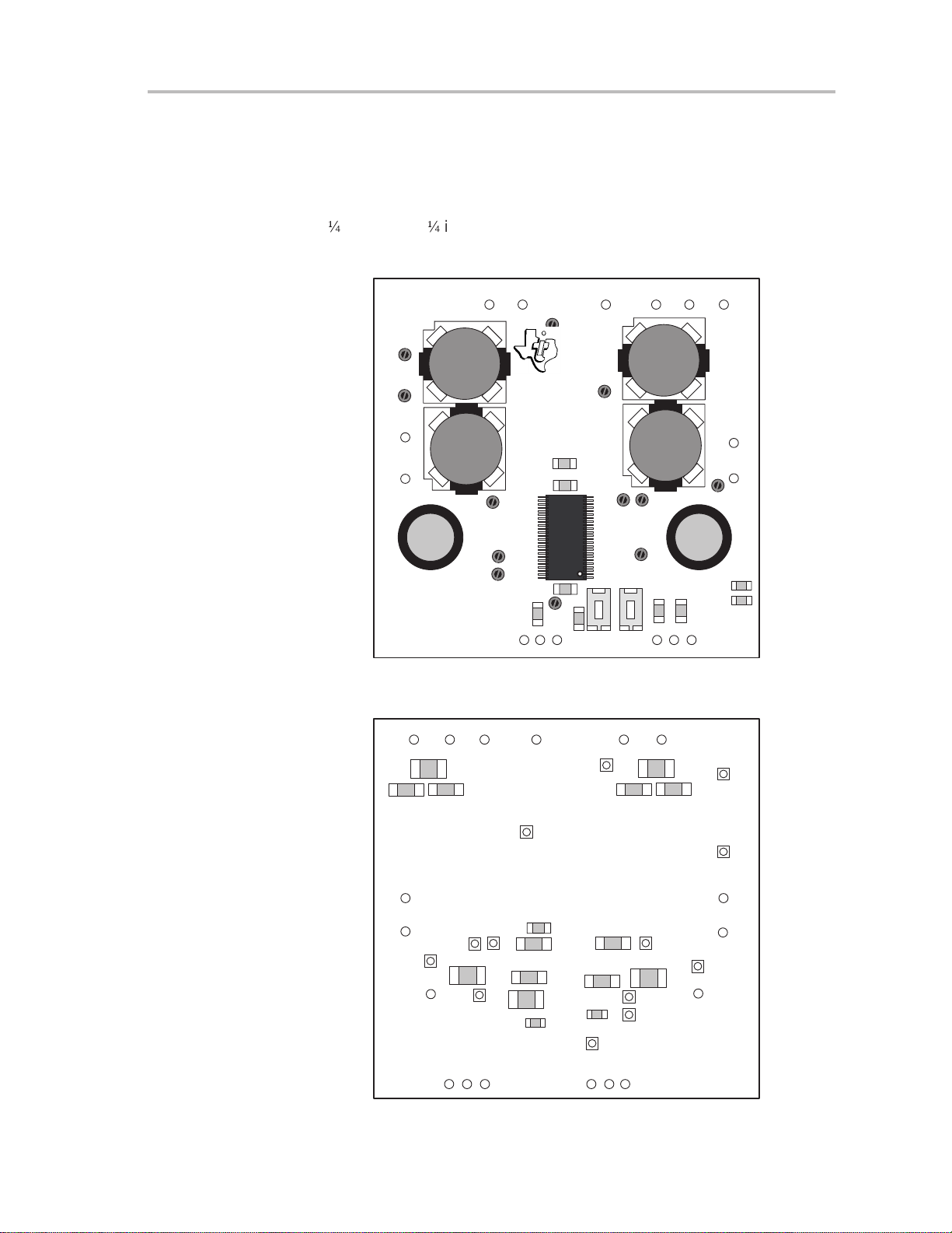
1.2 Description
Description
The TP A005D12 class-D stereo audio power amplifier evaluation module is a
complete, 2-Watt per channel stereo audio power amplifier. It consists of the
TI TPA005D12 class-D stereo audio power amplifier IC along with a small
number of other parts mounted on a circuit board that measures approximately
2¼ inches by 2¼ inches (Figure 1–1 and 1–2).
Figure 1–1.The TI TPA005D12 Class-D Stereo Audio Power Amplifier EVM —
L4
TP11
TP9
GND
L2
VDD2
C14
SLOP246 TPA005D12 EVM Board
Rout+
+
TP7
TP3
TP2
GND
C18
C5
C4
Rout–
TP12
TP1
+RIN–
Mute
Texas
Instruments
1999
TP10
C19
U1
C1
SD
TP6
S2
TP5
TP4
S1
Mute
–LIN+GND
C3
Lout–
C13
C2
Lout+
L3
L1
TP8
+
R2
R1
SD
Figure 1–2.The TI TPA005D12 Class-D Stereo Audio Power Amplifier EVM —
Top View
GND
VDD
Bottom View
C20
C24
C9
C21
C10
C6
C8
C17
C15
C22
C11
C7
C16
C25
C12
Introduction
C23
1-3
Page 10

TPA005D12 Class-D EVM Specifications
Single in-line header pins extend from the underside of the module circuit
board to allow the EVM to either be plugged into the TI plug-n-play audio
Amplifier evaluation Platform, or to be wired directly into existing circuits and
equipment when used stand-alone.
The platform has room for a single TP A005D12 class-D evaluation module and
is a convenient vehicle for demonstrating TI’s audio power amplifier and
related evaluation modules. The EVM simply plugs into the platform, which
automatically provides power to the modules, interconnects them correctly,
and connects them to a versatile array of standard audio input and output jacks
and connectors. Easy-to-use configuration controls allow the platform and
EVMs to quickly model many possible end-equipment configurations.
There is nothing to build, nothing to solder, and nothing but the speakers
included with the platform to hook up.
1.3 TPA005D12 Class-D EVM Specifications
All measurements made with VDD = 5 V and RL = 4 Ω, unless otherwise noted.
1.3.1 Maximum
Supply voltage range, V
Supply current, I
DD
Continuous output power per channel, BTL, P
Audio input voltage, V
DD
I
1.3.2 Typical
Supply current, no input, I
Supply current, EVM mute, I
Supply current, EVM shutdown, I
Gain
20 dB. . . . . . . . . . . . . . . . . . . . . . . . . . . . . . . . . . . . . . . . . . . . . . . . . . . . . . . . . . . . . . . . . . . . . . . .
Crosstalk, P
= 2 W @ 1 kHz –60 dB. . . . . . . . . . . . . . . . . . . . . . . . . . . . . . . . . . . . . . . . . . . . . . . . .
O
Total harmonic distortion + noise, P
DD
DD
DD
4.5 V to 5.5 V. . . . . . . . . . . . . . . . . . . . . . . . . . . . . . . . . . . . . . . . . . . . . .
2 W. . . . . . . . . . . . . . . . . . . . . . . . . . . . . . . . . . . . .
O
= 1 W @ 1 kHz 0.1 %. . . . . . . . . . . . . . . . . . . . . . . . . . . . . . .
O
2.3 A. . . . . . . . . . . . . . . . . . . . . . . . . . . . . . . . . . . . . . . . . . . . . . . . . . . . . . . . . . . .
280 mVrms. . . . . . . . . . . . . . . . . . . . . . . . . . . . . . . . . . . . . . . . . . . . . . . . . . . .
35 mA. . . . . . . . . . . . . . . . . . . . . . . . . . . . . . . . . . . . . . . . . . . . . . . . . .
2.5 mA. . . . . . . . . . . . . . . . . . . . . . . . . . . . . . . . . . . . . . . . . . . . . . . .
50 µA. . . . . . . . . . . . . . . . . . . . . . . . . . . . . . . . . . . . . . . . . . . . .
1-4
Introduction
Page 11
Chapter 2
Quick Start
Follow the steps in this chapter to quickly prepare the TPA005D12 class-D
stereo audio amplifier EVM for use. Using the TP A005D12 class-D EVM with
the TI plug-n-play audio amplifier evaluation platform is a quick and easy way
to connect power, signal and control inputs, and signal outputs to the EVM
using standard connectors. However, the audio amplifier evaluation module
can be used stand-alone by making connections directly to the module pins,
and it can be wired directly into existing circuits or equipment.
The platform switch and jumper settings shown in T able 2–1 are typical for the
TPA005D12 class-D EVM. There are no jumpers or switches to set on
the TPA005D12 class-D EVM board, itself.
Table 2–1. Typical TI Plug-N-Play Platform Jumper and Switch Settings for the
TPA005D12 Class-D EVM
POWER TYPE (Note 2) JP4 JP5 JP6 JP7 JP8 S1 S2 (Note3) S3
VDD (J6) X ON Mute X Lo X OFF U5
Notes: 1) ON = Jumper installed, OFF = Jumper
2) Unregulated and battery sources must have a voltage regulator EVM (SLVP097) installed in platform socket U6 (see
table 3–4, Section 3.5.5 for these options).
3) Set to ON when tone control board SLOP109 is installed in U1.
NOT
Installed, X = Don’t care
T opic Page
2.1 Precautions 2–2. . . . . . . . . . . . . . . . . . . . . . . . . . . . . . . . . . . . . . . . . . . . . . . . . .
2.2 Quick Start List for Platform 2–3. . . . . . . . . . . . . . . . . . . . . . . . . . . . . . . . . . .
2.3 Quick Start List for Stand-Alone 2–5. . . . . . . . . . . . . . . . . . . . . . . . . . . . . . . .
Quick Start
2-1
Page 12
Precautions
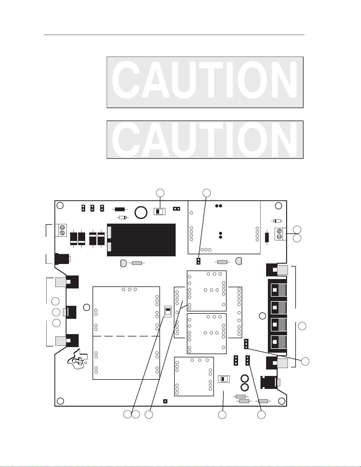
2.1 Precautions
Power Supply Input Polarity and Maximum Voltage
Always ensure that the polarity and voltage of the external power
connected to VCC power input connector J1, J2, and/or VDD power
input connector J6 are correct. Overvoltage or reverse-polarity
power applied to these terminals can open onboard soldered-in
fuses and cause other damage to the platform, installed evaluation
modules, and/or the power source.
Inserting or Removing EVM Boards
Do not insert or remove EVM boards with power applied — damage
to the EVM board, the platform, or both may result.
Figure 2–1.
In
+
Power
Audio
Input
Input
In
9
10
14
Quick Start Platform Map
SOURCE
J1
VCC
D4
AC/DC
J2
Right
In
Stereo
In
Left
In
INSTRUMENTS
1997
J3
J4
J5
JP2
JP1
DC
VCC(J1)
AC/DC
(J2)
Batt
D1
D2
D3
Signal Conditioning
Do not insert or remove
EVM boards with power
TEXAS
Plug-N-Play Audio Amplifier
Evaluation Platform
SLOP097 Rev. C.1
JP3
VR1
F1
VCC
C1+
LED1
****CAUTION****
applied
R1
U1
Off Pwr
1
GND
On
S1
Audio
Power
Amps
OnOff
ConditioningS2
TP1
ICC
JP4
B1
IDD
U5
8
JP5
U3 U4
R2
U2-U4
U5
HP
Source
SUPPLY
U2
HP(U5)
S3
R4
POWER
U6
LED2
VDD
JP6
Polarity
Lo
Hi
JP7
+
+
R3
J7
Out
Out
Out
Mode
Mute
Spk(U2-U4)
Out
JP8
C3 C2
HP Out
F2
Right
J8
+– +–
Right
Left
J9
Left
Stereo
In/Out
VDD
J10
R5
J6
VR2
DC
Power
In/Out
7
12
+
Speaker
Output
11
Headphone
Output
5
2-2
13
3
2
4 6
Quick Start
Page 13
2.2 Quick Start List for Platform
Follow these steps when using the TPA005D12 class-D EVM with the TI
plug-n-play audio amplifier evaluation platform (see the platform user’s guide,
SLOU011, for additional details). Numbered callouts for selected steps are
shown in Figure 2–1 and details appear in Chapter 3.
-
Platform Preparations
Quick Start List for Platform
1) Ensure that all external power sources are set to
OFF
.
2) Install a TP A005D12 module in platform socket U2, taking care to align the
module pins correctly (EVM power pins engage sockets U2 and U3).
3) Set switch S2 to
OFF
.
4) Set switch S3 to U5.
5) Set jumper JP6 to select the
6) Set control signal Polarity jumper JP8 to
Mute
control input.
Lo.
Table 2–2. Platform Jumper and Switch Settings for the TPA005D12
POWER TYPE (Note 2) JP4 JP5 JP6 JP7 JP8 S1 S2 (Note 3) S3
VDD (J6) X ON Mute X Lo X OFF U5
Notes: 1) ON = Jumper installed, OFF = Jumper
2) Unregulated and battery sources must have a voltage regulator EVM (SLVP097) installed in platform socket U6.
3) Set to ON when tone control board SLOP109 is installed in U1.
-
Power supply
7) Connect a
OFF
) to J6, taking care to observe marked polarity.
8) Set jumper JP5 for VDD power to EVMs.
-
Inputs and outputs
NOT
Installed, X = Don’t care
5-V
regulated power supply (ensure power supply is set to
9) Ensure that the audio signal source level is set to minimum.
10) Connect the audio source to left and right RCA phono jacks J3 and J5 or
stereo miniature phone jack J4.
11) Connect 4-Ω – 8-Ω speakers to left and right RCA jacks J7 and J9 or to
stripped wire speaker connectors J8.
-
Power up
12) Verify correct voltage and input polarity and set the external power supply
to
ON.
Platform LED2 should light indicating the presence of VDD, and the evaluation
module(s) installed on the platform should begin operation.
13) Set switch S2 to ON if tone control board SLOP109 is installed in U1.
14) Adjust the signal source level as needed.
Quick Start
2-3
Page 14

Quick Start List for Stand-Alone
2.3 Quick Start List for Stand-Alone
Follow these steps to use the TPA005D12 class-D EVM stand-alone or to
connect it into existing circuits or equipment. Connections to the TP A005D12
module header pins can be made via individual sockets, wire-wrapping, or
soldering to the pins, either on the top or the bottom of the module circuit board.
-
Power supply
1) Ensure that all external power sources are set to
OFF.
2) Connect an external regulated power supply set to 5 V to the module VDD,
VDD2, and GND pins taking care to observe marked polarity. It is only
necessary to use the ground pins adjacent to the module power pins.
-
Inputs and outputs
3) Ensure that audio signal source level adjustments are set to minimum.
4) Connect the audio source to the module RIN+/RIN– and LIN+/LIN– pins
for class-D operation, taking care to observe marked polarity. For
single-ended input, the negative input pins (RIN– and LIN–) should be
connected to the ground of the audio signal source.
5) Connect a control signal to the module Mute pin, if necessary . The control
signal should be high (2 V to 5 V or left floating) for normal operation, or
low (tied to ground) to mute the output.
6) Connect a control signal to the module SD pin, if necessary. The control
signal should be high (2 V to 5 V or left floating) for normal operation, or
low (tied to ground) to shut down the TPA005D12 amplifier IC on the EVM.
Note that the control signals applied to the EVM mute and SD inputs must have
sufficient current capability to overcome the 100-kΩ pullup resistor on each
input. Miniature pushbutton switches on the EVM allow manual shutdown (S2)
and manual muting (S1) of the amplifier.
2-4
7) Connect a 4-Ω – 8-Ω speaker to the module Rout+/Rout– pins and
another speaker to the Lout+/Lout– pins, taking care to observe marked
polarity .
-
Power up
8) Verify correct voltage and input polarity and set the external power supply
to
ON.
The EVM should begin operation.
9) Adjust the signal source level as needed.
Quick Start
Page 15

Chapter 3
Details
This chapter provides details on the TPA005D12 IC, the evaluation module,
and the steps in the Quick-Start list, a discussion of class-D amplifiers,
additional application information, a parts list for the TPA005D12 class-D
evaluation module, module performance graphs, and module PCB layer
illustrations.
Topic Page
3.1 Precautions 3-2. . . . . . . . . . . . . . . . . . . . . . . . . . . . . . . . . . . . . . . . . . . . . . . . . .
3.2 The TPA005D12 Class-D Audio Power Amplifier EVM 3-3. . . . . . . . . . . .
3.3 Class-D Amplifier Design Considerations 3-10. . . . . . . . . . . . . . . . . . . . . .
3.4 Using The TPA005D12 Class-D EVM With the P-N-P Platform 3-11. . . .
3.5 Using The TPA005D12 Class-D EVM Stand-Alone 3-18. . . . . . . . . . . . . . .
3.6 TP A005D12 Class-D EVM Performance Characteristics 3-20. . . . . . . . . .
3.7 TP A005D12 Class-D EVM Interconnects 3-24. . . . . . . . . . . . . . . . . . . . . . . .
3.8 TP A005D12 Class-D Evaluation Module Parts List 3-25. . . . . . . . . . . . . .
3.9 TP A005D12 Class-D EVM Schematic 3-26. . . . . . . . . . . . . . . . . . . . . . . . . . .
3.10 TPA005D12 Class-D EVM PCB Layers 3-27. . . . . . . . . . . . . . . . . . . . . . . . .
Details
3-1
Page 16

Precautions
3.1 Precautions
Power Supply Input Polarity and Maximum Voltage
Always ensure that the polarity and voltage of the external power
connected to VCC power input connector J1, J2, and/or VDD power
input connector J6 are correct. Overvoltage or reverse-polarity
power applied to these terminals can open onboard soldered-in
fuses and cause other damage to the platform, installed evaluation
modules, and/or the power source.
Inserting or Removing EVM Boards
Do not insert or remove EVM boards with power applied — damage
to the EVM board, the platform, or both may result.
Figure 3–1.The TI Plug-N-Play Audio Amplifier Evaluation Platform
On
R1
U1
Off Pwr
S1
Audio
Power
Amps
ConditioningS2
ICC
JP4
B1
JP5
IDD
U3 U4
OnOff
Power
Input
Audio
Input
+
In
VCC
In
AC/DC
J1
D4
J2
In
In
In
SOURCE
DC
VCC(J1)
D3
Right
J3
Stereo
J4
Left
J5
JP2
JP1
AC/DC
(J2)
D2
D1
Batt
JP3
VR1
Signal Conditioning
F1
VCC
C1+
LED1
R2
SUPPLY
U2
POWER
U6
LED2
VDD
Out
J7
Right
J8
Out
Out
F2
+– +–
Right
Left
In/Out
VDD
J6
VR2
+
DC
Power
In/Out
Speaker
Output
3-2
TEXAS
INSTRUMENTS
1997
Plug-N-Play Audio Amplifier
Evaluation Platform
SLOP097 Rev. C.1
****CAUTION****
Do not insert or remove
EVM boards with power
applied
GND
TP1
U5
U2-U4
U5
HP
Source
HP(U5)
S3
R4
JP6
Polarity
Lo
Hi
JP7
+
+
R3
Mode
Mute
Spk(U2-U4)
Out
JP8
C3 C2
HP Out
J9
Left
Stereo
J10
R5
Headphone
Output
Details
Page 17

The TP A005D12 Class-D Audio Power Amplifier Evaluation Module
3.2 The TPA005D12 Class-D Audio Power Amplifier Evaluation Module
The TPA005D12 class-D stereo audio power amplifier evaluation module is
powered by a TPA005D12 class-D stereo power amplifier integrated circuit.
The EVM is capable of delivering greater than 2 W of continuous average
power per channel into 4-Ω loads at less than 0.6% THD+N over a 20-Hz to
20-kHz frequency range from a 5-V supply.
The TP A005D12 amplifier IC operates in the bridge-tied load (BTL) mode for
maximum efficiency during class-D operation. The high IC switching
frequency reduces the size of the output filter to three small capacitors and two
small inductors per class-D channel. The evaluation module includes onboard
pushbutton switches for manual muting and shutdown, and input pins for logic
control of mode, mute, and shutdown.
The module can be used with the TI plug-n-play audio amplifier evaluation
platform (Figure 3–1) or wired directly into circuits or equipment. The module
has single in-line header connector pins mounted to the underside of the
board. These pins allow the module to be plugged into the platform, which
automatically makes all the signal input and output, power, and control
connections to the module.
The module connection pins are on 0.1-inch centers to allow easy use with
standard perf board and plug board-based prototyping systems. Or, the EVM
can be wired directly into existing circuits and equipment when used
stand-alone.
The module appears in Figure 3–2 (top side) and Figure 3–3 (bottom side),
and its schematic is shown in Figure 3–4. Note that several components are
mounted on the bottom side of the EVM PCB.
Details
3-3
Page 18
The TP A005D12 Class-D Audio Power Amplifier Evaluation Module
Figure 3–2.The TI TPA005D12 Class-D Stereo Audio Power Amplifier EVM —
L4
TP11
TP9
GND
L2
VDD2
C14
SLOP246 TPA005D12 EVM Board
Rout+
+
TP7
TP3
TP2
GND
C18
C5
C4
Rout–
TP12
TP1
+RIN–
Mute
Texas
Instruments
1999
TP10
C19
U1
C1
SD
TP6
S2
TP5
TP4
Mute
S1
Lout–
C13
C3
C2
–LIN+GND
Lout+
L3
L1
TP8
+
R2
R1
SD
Figure 3–3.The TI TPA005D12 Class-D Stereo Audio Power Amplifier EVM —
Top View
GND
VDD
Bottom View
C20
C24
C9
C21
C10
C6
C8
C17
C15
C11
C7
C22
C25
C23
C16
C12
3-4
Details
Page 19

The TP A005D12 Class-D Audio Power Amplifier Evaluation Module
Figure 3–4.TPA005D12 Class-D EVM Schematic Diagram
VDD
1µF
1µF
470pF
1µF
R2
100k
1
SHUTDOWN
2
MUTE
3
AGND
4
LINN
5
LINP
6
LCOMP
7
AGND
8
VDD
9
LPVDD
10
LOUTP
11
LOUTP
12
PGND
13
PGND
14
LOUTN
15
LOUTN
16
LPVDD
17
NC
18
NC
19
NC
20
AGND
21
PVDD
22
VCP
23
CP3
24
CP2
TPA005D12
RCOMP
FAULT_0
FAULT_1
RPVDD
ROUTP
ROUTP
ROUTN
ROUTN
RPVDD
0.047µF
C18
C19
0.047µF
COSC
AGND
AGND
RINN
RINP
PGND
PGND
NC
NC
NC
V2P5
PVDD
PGND
CP4
CP1
48
47
46
45
44
43
42
41
40
39
38
37
36
35
34
33
32
31
30
29
28
27
26
25
1µF
1µF
470pF
TP2
TP3
SD
Mute
LIN–
LIN+
C13 C9 C10
VDD
LOUT+
LOUT–
VDD
10µF
C24
1µF
R1
100k
S1
Mute
1µF
C20
0.22µF
C21
0.22µF
C15
1µF
S2
SD
C3
C2
C6
C8
L1
15µH
L3
15µH
C17
0.1µF
C1
C4
C7
L2
15µH
L4
15µH
C16
1µF
C5
470pF
C23
0.22µF
C22
0.22µF
1µF
10µF
C25
1µF
VDD
VDD2
+5V
+5V
TP2
TP3
RIN–
RIN+
C14C12C11
VDD2
ROUT+
ROUT–
3.2.1 TPA005D12 Class-D Stereo Audio Amplifier IC
The TPA005D12 class-D stereo audio power amplifier integrated circuit
converts low-level audio into pulse-width-modulated (PWM) signals, which
result in an audio output with a 20-dB increase in amplitude. The IC features
high-current DMOS output transistors and internal feedback that provides
excellent performance without the need for external components (beyond
input isolation and output filtering).
A full range of protection features are built into the TP A005D12 amplifier IC to
increase device reliability: thermal, overcurrent, and undervoltage shutdown,
with status terminals that report any error conditions encountered.
The device is provided in a very small 48-pin thermally-enhanced PowerP AD
TSSOP surface-mount package (DCA) and consumes only 1 µA in the
shutdown mode, making the TPA005D12 an excellent choice for portable
battery-powered applications.
Details
3-5
Page 20

The TP A005D12 Class-D Audio Power Amplifier Evaluation Module
3.2.2 Overview of Class-D Audio Amplifiers
Class-D audio amplifiers are very similar in operation to switch-mode power
supplies in that both compare an input signal with a reference to create an error
voltage that controls a pulse-width modulator (PWM) circuit. The PWM circuit
then produces an output signal at constant frequency and with a duty cycle that
varies according to the input signal. A block diagram of the major components
that make up the amplifier is shown in Figure 3–5.
Figure 3–5.Class-D Functional Diagram
Audio
Analog
Source
Ramp
Generator
V
CONTROL
V
OUT
H-Bridge
Load
V
V
RAMP
V
Comparator
IN
ERROR
PWM
Control
LPF
The audio input signal (VIN) is applied to a very fast comparator along with a
ramp signal (V
) created by the ramp generator. Each time the triangle
RAMP
wave from the ramp generator crosses the audio input signal level, the
comparator sends an error signal (V
PWM control signal (V
CONTROL
ERROR
) then regulates the duty cycle of the
) to the PWM control circuit. The
high-current DMOS power transistors of the H-bridge, providing the output
signal (V
OUT
).
These transistors operate in either the cutoff or saturated regions, rather than
the linear region, which is where class AB amplifiers operate. This reduces
switching and conduction losses, reducing the power dissipated by the power
transistors and allowing more power to be delivered to the load. An
inductor-capacitor (LC) low-pass filter (LPF) then removes the high frequency
switching component from V
, leaving an amplified version of the original
OUT
input signal. Examples of these waveforms are shown in Figure 3–6.
3-6
Details
Page 21

The TP A005D12 Class-D Audio Power Amplifier Evaluation Module
Figure 3–6.Class-D Input and Output Waveforms
V
RAMP
V
0 V
DD
V
OUT
V
IN
The V
signal must be at a much higher frequency than the highest
RAMP
frequency component of VIN to obtain an accurate representation at the
low-pass filter output and allow greater attenuation of the switching
component of V
. The TPA005D12 class-D EVM uses a 250 kHz V
OUT
signal to sample VIN. This frequency is more than ten times higher than the
highest frequency component of the 20 Hz to 20 kHz range of the audio input,
providing excellent output resolution and easy filtering by the LPF.
3.2.3 Bridge-Tied Load (BTL) Operation
The DMOS output transistors of the TPA005D12 class-D amplifier IC are
arranged in an H-bridge configuration to allow BTL operation. In the BTL
output mode, each half of the H-bridge operates 180° out of phase from the
other. The load, in this case, a speaker, is then connected between the two
halves, and is not connected directly to ground. The load is, in a sense,
floating.
BTL operation has two main advantages over single-ended operation. First,
it eliminates the need for a bulky output coupling capacitor to block any dc
offset voltage that may be present (which reduces the speaker response and
may damage the speaker). And second, it quadruples the output power that
can be delivered to the load. For more information, see the TPA005D12
amplifier IC data sheet, TI Literature Number SLOS240.
RAMP
To operate in the BTL output mode, the EVM output signal from Rout+/Lout+
must go through the speaker load and be returned directly
NOT
to Rout–/Lout–, and
to system ground. This requires that the Rout–/Lout–
lines be isolated not only from system ground, but also from each other and
the out– lines of any other amplifiers in the system. The plug-n-play platform
provides such isolated output lines, connecting the EVM output pins directly
to left and right speaker connectors.
Details
3-7
Page 22

The TP A005D12 Class-D Audio Power Amplifier Evaluation Module
3.2.4 Class-D Differential Inputs
The TP A005D12 EVM line inputs allow the use of a single-ended or differential
audio source. The differential input stage of the amplifier cancels any noise
that appears on both input lines of a channel. T o use the EVM with a differential
source, connect the positive lead of the audio source to the RIN+/LIN+ inputs
and the negative lead to the RIN–/LIN– inputs. To use the EVM with a
single-ended source, connect the positive lead of the audio source to the
RIN+/LIN+ inputs and the ground lead to the RIN–/LIN– inputs. This ac
grounds the input capacitors on the negative terminals and balances the input
impedance of the class-D amplifier’s positive and negative input terminals,
preventing voltage differences that result in popping in the speakers.
3.2.5 Control and Indicator Circuits
Three main control circuits are provided with the TP A005D12. The mute circuit
grounds the output of the active amplifier, and the shutdown circuit places the
entire device into a power-saving sleep mode to minimize current
consumption. Each of these inputs is TTL compatible: less than 0.8 V applied
to these pins is considered a logic low, and any voltage greater than 2 V is
considered a logic high.
Two indicator pins are also provided for feedback when an under-voltage,
over-current, or thermal fault exists. Module pins are provided for easy
connection of off-board control and monitoring. There are two active low fault
indicator pins on the TP A005D12 amplifier IC (IC pins 40 and 41) that provide
feedback when a fault condition exists. Signals on these pins provide the
status of the class-D amplifier: operational, over-current, thermal fault, and
under-voltage lockout. Table 3–1 lists the possible output conditions of these
pins and a description of the fault indicated.
Table 3–1.TPA005D12 Class-D EVM Fault Indicator Table
FAULT 0
(TP 2)
1 1 No fault. — The device is operating normally.
1 0 Charge pump under-voltage lockout (VCP-UV) fault — the charge pump voltage is < (PVDD + 6V).
0 1 Over-current fault — the output current limit has been exceeded. All output transistors are switched
0 0 Thermal fault — the internal junction temperature has exceeded 125°C. All of the low-side
FAULT 1
(TP 3)
DESCRIPTION
All low-side transistors are turned on, shorting the load to ground. Normal operation resumes when
the charge pump voltage is restored (not a latched fault), however the Fault
active until cleared by cycling MUTE
off, causing the load to see a high impedance state. This is a
MUTE
, SHUTDOWN, or the power supply.
transistors are turned on, shorting the load to ground. Once the junction temperature drops by 20°C
and is below 125°C, normal operation resumes (not a latched fault). The Fault
active until cleared by cycling MUTE
, SHUTDOWN, or the power supply.
latched
fault and is cleared by cycling
, SHUTDOWN, or the power supply.
indication
indication
remains
remains
3-8
Details
Page 23

The TP A005D12 Class-D Audio Power Amplifier Evaluation Module
3.2.6 TPA005D12 Class-D EVM Test Points
Test points have been included on the TPA005D12 class-D EVM to facilitate
user analysis of device performance and design adjustments. Table 3–2 lists
each test point and its corresponding function.
Table 3–2.TPA005D12 Class-D EVM Test Points
TEST
POINT
IC PIN or EVM
FUNCTION
1 COSC Ramp generation capacitor input and output
2 FAULT_0 LSB for logic-level fault output signal, open drain
3 FAULT_1 MSB for logic-level fault output signal, open drain
4 N/A Probe ground connections
5 LOUTP Class-D left channel positive output of the H-bridge
6 VCP Charge pump storage capacitor
7 ROUTP Class-D right channel positive output of the H-bridge
8 VDD Probe VDD power input connections
9 VDD2 Probe VDD2 power input connections
10 LOUTN Class-D left channel negative output of the H-bridge
11 ROUTN Class-D right channel negative output of the H-bridge
12 N/A Probe ground connections
FUNCTION
Details
3-9
Page 24

Class-D Amplifier Design Considerations
3.3 Class-D Amplifier Design Considerations
Detailed information for proper design and implementation of TI class-D audio
power amplifiers appears in the application report
Class-D Audio Power Amplifiers
website (http://www.ti.com/sc/apa). This document provides background
information, general equations, and component selection criteria for the topics
listed below. General layout considerations are also included in the report.
-
Class-D amplifier circuits (input, output, charge pump, and switching)
-
Control and indicator circuits
-
Power supply decoupling
, TI Literature Number SLOA031, on the TI
Design Considerations for
The application report
Reducing and Eliminating the Class-D Output Filter
SLOA023, is also available from the website, and provides information to help
determine what type of output filter, if any, may be necessary.
,
3-10
Details
Page 25

Using The TPA005D12 Class-D EVM With the Plug-N-Play Platform
3.4 Using The TPA005D12 Class-D EVM With the Plug-N-Play Platform
The TPA005D12 class-D stereo audio amplifier evaluation module was
designed to be used with the TI plug-n-play audio amplifier evaluation
platform. It simply plugs into socket U2 and U3.
The following paragraphs provide additional details for using the TP A005D12
class-D EVM with the platform.
3.4.1 Installing and Removing EVM Boards
TI plug-n-play evaluation modules use single-in-line header pins installed on
the underside of the module circuit board to plug into sockets on the platform.
The EVM pins and the platform sockets are keyed such that only the correct
type of EVM can be installed in a particular socket, and then only with the
proper orientation.
Evaluation modules are easily removed from the platform by simply prying
them up and lifting them out of their sockets. Care must be taken, however, to
prevent bending the pins.
3.4.1.1 EVM Insertion
3.4.1.2 EVM Removal
1) Remove all power from the evaluation platform.
2) Locate sockets U2 and U3 on the platform.
3) Orient the module correctly.
4) Carefully align the pins of the module with the socket pin receptacles.
5) Gently press the module into place.
6) Check to be sure that all pins are seated properly and that none are bent
over.
1) Remove all power from the evaluation platform.
2) Using an appropriate tool as a lever, gently pry up one side of the module
a small amount.
3) Change to the opposite side of the module and use the tool to pry that side
up a small amount.
4) Alternate between sides, prying the module up a little more each time to
avoid bending the pins, until it comes loose from the socket.
5) Lift the EVM off of the platform.
Details
3-11
Page 26

Using The TPA005D12 Class-D EVM With the Plug-N-Play Platform
3.4.2 Module Switches
The TPA005D12 class-D stereo audio amplifier evaluation module is
equipped with two pushbutton switches that allow the module shutdown and
mute functions to be manually activated.
3.4.2.1 S1 — Shutdown
To have the module amplifier IC enter the shutdown mode, press the
Shutdown switch (S2) on the module. S2 connects the amplifier IC
SHUTDOWN
be controlled by an external control input to the SD module pin.
The shutdown mode reduces the amplifier IC current consumption to
approximately 1 µA compared to approximately 2.5 mA in the mute mode. The
EVM shutdown current is based on V
but will typically be 50 µA ±5% for VDD = 5 V . The plug-n-play platform typically
draws 23 mA of current.
3.4.2.2 S2 — Mute Switch
Pushbutton switch S1 on the TP A005D12 class-D EVM allows manual muting
of the amplifier IC. S1 connects the amplifier IC MUTE pin to ground, muting
the output. The EVM Mute control input pin also allows external control of this
function.
pin to ground, forcing it into a low-power state. This function can
R2, and capacitor leakage currents,
DD,
In the mute mode, the amplifier IC lowside output transistors are turned on,
shorting the load to ground. This reduces the EVM current to 2.5 mA.
3-12
Details
Page 27

Using The TPA005D12 Class-D EVM With the Plug-N-Play Platform
3.4.3 Signal Routing
Signal flow on the platform is controlled by two signal routing switches, as
shown in Figure 3–7.
Figure 3–7.Platform Signal Routing and Outputs
Off
R
Audio
Input
L
U1
Signal
Conditioning
S2
On
U2/U3
TPA005D12
Amplifier EVM
U5
Stereo
Headphone
Amplifier
+
GND
R
L
R
L
–
J7, J8, J9
Speaker
Outputs
–
+
+
–
Headphone
Output
–
+
J10
R
L
U2–U4
R
S3
L
U5
3.4.3.1 Signal Conditioning
The audio signal from input jacks can be applied to the signal conditioning
socket (U1) if an EVM is installed there, or socket U1 can be bypassed and the
audio input signal applied directly to the inputs of the TPA005D12 class-D
EVM.
-
Platform switch S2 selects signal conditioning or bypasses it.
3.4.3.2 Headphone Output Jack
Switch S3 is the source select for the stereo headphone output jack, J10. The
headphone jack is capacitively coupled (via 470 µF electrolytics) and can
output either the signal from the headphone amplifier in socket U5, or the
signal from the power amplifier installed in socket U2, as determined by the
setting of headphone source select switch S3.
-
The platform headphone output jack (J10) is not used in conjunction with
the TP A005D12 class-D EVM. Switch S3 should be set to the U5 position
when the TPA005D12 class-D EVM is installed on the platform.
Details
3-13
Page 28

Using The TPA005D12 Class-D EVM With the Plug-N-Play Platform
3.4.4 Shutdown
The TP A005D12 class-D EVM is equipped with a shutdown control input pin.
When this input is tied to GND, the TPA005D12 amplifier IC on the module
enters the shutdown mode and dissipates very little power. When the EVM
control input is tied to VDD or allowed to float, amplifier operation resumes.
In typical applications, as often found in notebook computers and other
portable audio products, the internal speakers mute when headphones are
plugged into the headphone jack, or internal speakers mute when external
speakers are connected. In applications using separate speaker and
headphone amplifiers, the one not being used can be muted to conserve
power.
The TP A005D12 EVM shutdown control pin connects to the platform Mute line
of JP6 when the EVM is inserted in the plug-n-play platform. When JP6 is set
to Mute and JP8 is set to Lo, the class-D EVM will operate normally until a
headphone plug is inserted into platform jack J10 and the class-D amplifier is
placed into shutdown. Once the jack is removed from J10, the class-D EVM
again becomes active. Note that when JP6 is set to mute and the class-D EVM
shutdown pin is activated, the platform current increases by approximately 20
mA. This current is set by the connection of the 240-Ω platform resistor (R3)
to ground through the EVM shutdown switch.
3.4.4.1 Headphone Jack Control Signals
The platform headphone output jack (J10) contains an internal switch that
changes the state of a pair of control lines when a plug is inserted (Figure 3–8).
Each control line is pulled down by a 1-kΩ resistor to ground (R4 and R5). The
switch in the headphone jack pulls one line or the other up to VDD through a
240-Ω resistor (R3) depending on whether a plug is inserted in J10 or not.
Figure 3–8.Mute/Mode and Polarity Control
V
DD
R3
240 Ω
J10
Headphone
Jack
R4
1 kΩ
R5
1 kΩ
Polarity
JP8 JP6
Lo
Hi
SPK
(U2–U4)
Mode
Mute
U2
Power
Amplifier
3-14
Details
Page 29

Using The TPA005D12 Class-D EVM With the Plug-N-Play Platform
3.4.4.2 Mute/Mode Select (JP6)
A 3-pin jumper header (JP6) on the platform, functioning as an SPDT switch,
routes the control signal from the headphone jack to either the mute control
input pin or the mode control input pin of the evaluation module.
J
Set jumper JP6 to
NOT
installed in U5
J
Set jumper JP6 to
installed in U5. This will cause the TP A005D12 class-D EVM to shut
down when a plug is inserted into platform headphone jack J10.
3.4.4.3 Mute/Mode Polarity Select (JP8)
A second 3-pin jumper header (JP8) on the platform selects the control signal
polarity by connecting either the active-high or the active-low line from the
headphone jack to jumper JP6.
-
Set jumper JP8 to Lo for normal class-D operation when a separate
headphone amplifier IS installed in U5
MODE
when a separate headphone amplifier is
.
MUTE
when a separate headphone amplifier
.
IS
Details
3-15
Page 30

Power Requirements
3.4.5 Power Requirements
The TPA005D12 class-D stereo audio power amplifier evaluation module is
designed to operate from a supply voltage between 4.5 V and 5.5 V . For best
performance (highest output power with lowest distortion), the module should
be operated at 5 V.
The TI plug-n-play audio amplifier evaluation platform provides several
options for powering the TPA005D12 class-D EVM. Table 3–3 shows the
platform
jumper and switch settings for each power source option (see the
User’s Guide for the TI plug-n-play audio amplifier platform, TI Literature
Number SLOU011 for more information). The TPA005D12 class-D EVM
requires no setup for power source selection.
Table 3–3.Platform Jumper and Switch Settings for the TPA005D12 EVM Power Inputs
POWER TYPE (Note 2) JP1 JP2 JP3 JP4 JP5 JP6 JP7 JP8 S1 S2 S3
VCC (J1) ON OFF OFF ON ON Mode X Hi ON Note 3 U5
AC/DC (J2) OFF ON OFF ON ON Mode X Hi ON Note 3 U5
Battery (B1) OFF OFF ON ON ON Mode X Hi ON Note 3 U5
VDD (J6) OFF OFF OFF X ON Mode X Hi ON Note 3 U5
Notes: 1) ON = Jumper installed, OFF = Jumper
2) Unregulated and battery sources must have a voltage regulator EVM (SLVP097) installed in platform socket U6.
3) Set to ON when Tone Control Board SLOP109 is installed in U1, otherwise set to OFF..
NOT
Installed, X = Don’t care
Although the TP A005D12 amplifier IC draws approximately 0.7 A per channel
from the power supply during continuous full power output, peak current draw
can be as high as 1.15 A per channel. Any power supply connected to the
platform should be capable of providing 2.3 A to avoid clipping of the output
signal during voltage peaks. Current consumption driving speakers at normal
listening levels is typically 0.1 A or less.
supply of 5 V is required if a signal processing EVM is installed in
A V
DD
platform socket U1 or a separate headphone amplifier EVM is installed in U5.
can either be applied to the platform VDD power input terminals (J6) or a
V
DD
voltage regulator (SLVP097 or equiv.) can be installed in platform socket U6
to provide VDD from the platform VCC supply.
The platform is equipped with overvoltage and reverse-polarity supply voltage
input protection in the form of fused crowbar circuits.
-
VDD voltage applied to platform screw terminals J6
MUST NOT
exceed
the absolute maximum rating for the TP A005D12 amplifier IC installed on
the evaluation module (5.5 V) or damage to the IC may result. In no case
should VDD voltage of the incorrect polarity or in excess of 6.0 V be applied
to screw terminals J6 of the platform, or the power protection circuit on the
line will trip.
V
DD
-
VCC voltage applied to the platform
MUST NOT
exceed the maximum
voltage input specified for the voltage regulator module installed in socket
U6 (12 V for the SLVP097), or damage to the voltage regulator module
may result. In no case should VCC voltage applied to the platform exceed
15 V, or the overvoltage protection circuit on the V
bus will trip.
CC
3-16
Details
Page 31

3.4.6 Inputs and Outputs
The TI plug-n-play audio amplifier evaluation platform is equipped with several
standard conectors for audio inputs and outputs.
3.4.6.1 Inputs
In most cases, audio signals enter the platform through either a pair of RCA
phono jacks (J3 and J5) or a miniature (1/8″) stereo phone jack (J4). Certain
signal conditioning and amplifier EVMs, however, may have additional signal
input connectors mounted on the module circuit board.
The platform audio signal input jacks (J3, J4, and J5) are of the closed-circuit
type, grounding the signal input lines when no plugs are inserted.
3.4.6.2 Outputs
Amplified audio output signals leave the platform through left and right RCA
phono jacks (J7 and J9), left and right pairs of compression connectors for
stripped speaker wires (J8), and optionally , through a miniature (1/8″) stereo
phone jack (J10), for headphones.
The audio output lines from the power amplifiers are separate all the way to
the edge of the platform (output jacks J7, J8, and J9)—the OUT– lines from
the power amplifier sockets are not tied to each other or to platform ground.
This allows the TPA005D12 class-D power amplifier EVM to operate in the
highly-efficient bridge-tied load configuration when driving speakers.
Inputs and Outputs
The headphone jack (J10) is capacitively coupled to source select switch S3,
which connects J10 to the output lines of either the headphone amplifier
socket or the power amplifier sockets (Figure 3–9).
Figure 3–9.Typical Headphone Plug
Left Right GND
Details
3-17
Page 32

Using The TPA005D12 Class-D EVM Stand-Alone
3.5 Using The TPA005D12 Class-D EVM Stand-Alone
Using the TPA005D12 class-D stereo audio power amplifier evaluation
module stand-alone is much the same as using it with the platform. The same
4.5-V to 5.5-V power supply range and the isolated out+ and out– lines for BTL
operation (Section 3.2.3) requirements exist. Figure 3–10 shows the
connections that are required for operation (with the exception of the fault
monitor circuit, which is optional). The discussion in this section is in reference
to this figure unless otherwise noted.
Figure 3–10. TPA005D12 Class-D EVM Stand-Alone Connections for Stereo BTL Output
5 V
Audio
Inputs
(Right)
Audio
Inputs
(Left)
Fault
Monitor
LED 1
R
R
LED 0
TP2
TP3
GND
C4
TP1
R1
C5
C3
C2
R2
SD
S2
Mute
S1
TP4
+RIN–
C1
–LIN+GND
5 V
SLOP246 TPA005D12 EVM Board
C14
VDD2
GND
L2
+
TP7
C18
C19
U1
TP6
TP5
C13
TP8
+
GND
VDD
TP9
1999
Instruments
Texas
TP10
L1
TP11
L4
Rout+
Right
Rout–
TP12
Mute
Mute
Shutdown
SD
Lout–
L3
Lout+
Left
3.5.1 Power Connections
Power must be connected to both the VDD and VDD2 module pins. Power
supply ground can be connected to any module ground pin, although best
results are achieved if power supply grounds are connected to the pins
adjacent to the VDD and VDD2 module pins. The ground and power wires
should be twisted to reduce inductance and noise pickup if they are long.
3-18
5 V
Details
Page 33

3.5.2 Input Connections
The class-D amplifier input signals can be connected in either of two ways:
differential or single-ended. For differential operation, connect the two lines
from the signal source to the positive and negative inputs of each channel
(RIN+/RIN– and LIN+/LIN– module pins). For single-ended operation, the
input signal lines should be connected to the RIN+ and LIN+ module pins and
the signal source ground wires should be connected to the RIN– and LIN–
module pins.
For best results, the ground of the signal source should be connected to the
GND pins at the EVM inputs to provide a return path for the current. The input
signal and ground wires should be twisted to reduce inductance and noise
pickup if the lead lengths are long and the cable is not shielded.
3.5.3 Output Connections
The right speaker should be connected between the Rout+ and the Rout–
module pins, and the left speaker should be connected between the Lout+ and
the Lout– module pins to comply with the isolated output requirements for BTL
operation.
Using The TPA005D12 Class-D EVM Stand-Alone
3.5.4 Controls and Indicators
The mute and shutdown functions may be controlled externally via the module
mute and SD pins. An active-low input mutes the selected amplifier or shuts
down the device. A signal of 2 V or higher, or a float condition, allows normal
operation.
Note that the mute and shutdown signals applied to the EVM control input pins
must be able to supply enough current to overcome the pullup resistor on the
module (100 kΩ).
The fault indicator circuit can be monitored by attaching a pullup resistor to the
open-drain outputs of FAULT0 (TP2) and FAULT1 (TP3). The voltage should
not exceed 5 V and the current must be limited to less than 1 mA. A fault table
is shown in Section 3.2.5 and the device data sheet.
Details
3-19
Page 34

TPA005D12 Class-D EVM Performance Characteristics
3.6 TPA005D12 Class-D EVM Performance Characteristics
The TP A005D12 class-D stereo audio power amplifier EVM was tested using
an Audio Precision System II, model 2322, a 5-V regulated dc power supply ,
and the TI PNP audio power amplifier evaluation platform set up as described
in Chapter 2. Results were obtained with 4-Ω and 8-Ω speaker loads. The
results are shown in Figures 3–11 through 3–17.
The frequency response shown in Figure 3–17 is a relatively flat 20 dB over
the 20 Hz to 100 kHz frequency range. The lower and upper frequency corners
can be adjusted to extend the frequency response.
Figure 3–11. Class-D Amplifier Frequency Response at 4
VOLTAGE AMPLIFICATION
22.5
20
17.5
15
12.5
10
7.5
5
Voltage Amplification – dB
2.5
VDD = 5 V
0
RL = 4 Ω
–2.5
TA = 25° C
–5
10 100 1k
FREQUENCY
f – Frequency – Hz
Ω
vs
10k 100k
3-20
Total harmonic distortion plus noise (THD+N) versus output power and
frequency is shown in Figures 3–12 through 3–15 below. Figures 3–12 and
3–13 show power sweeps at a fixed frequency of 1 kHz. Switching and input
noise begins to dominate at low power, while the distortion at the mid to upper
power levels is a function of the class-D amplifier and the inductor. The lower
frequency noise may be improved by either increasing the order of the filter or
by increasing the amplifier switching frequency , which will further attenuate the
switching noise in the audio band.
Midrange distortion is a combination of the switching noise of the output power
transistors in the IC and the magnetic field created by the inductors. This
distortion is minimized by good separation of the output filter inductors for each
channel and through good EMI-reduction layout techniques.
Details
Page 35

TPA005D12 Class-D EVM Performance Characteristics
Figure 3–12. Class-D Amplifier Distortion versus Output Power at 4
TOTAL HARMONIC DISTORTION PLUS NOISE
vs
OUTPUT POWER
1
VDD = 5 V
RL = 4 Ω
TA = 25° C
1 kHz
0.1
THD+N – Total Harmonic Distortion Plus Noise – (%)
0.02
0.01 1 2
PO – Output Power – W
0.1
Figure 3–13. Class-D Amplifier Distortion versus Output Power at 8
Ω
Ω
TOTAL HARMONIC DISTORTION PLUS NOISE
vs
OUTPUT POWER
1
VDD = 5 V
RL = 8 Ω
TA = 25° C
1 kHz
0.1
THD+N – Total Harmonic Distortion Plus Noise – (%)
0.02
0.01 1 2
PO – Output Power – W
0.1
Details
3-21
Page 36

TPA005D12 Class-D EVM Performance Characteristics
Figures 3–14 and 3–15 show a frequency sweep for a 1-W output. The lower
frequency distortion of the graphs is dominated by noise, while the distortion
at higher frequencies is due primarily to the fast-changing duty cycle of the
PWM output.
Figure 3–14. Class-D Amplifier Distortion versus Frequency at 1 W Into 4
TOTAL HARMONIC DISTORTION PLUS NOISE
vs
FREQUENCY
1
VDD = 5 V
RL = 4 Ω
PO = 1 W
TA = 25° C
0.1
THD+N – Total Harmonic Distortion Plus Noise – (%)
0.02
20 100 1k
f – Frequency – Hz
Ω
10k 20k
Figure 3–15. Class-D Amplifier Distortion versus Frequency at 1 W Into 8
TOTAL HARMONIC DISTORTION PLUS NOISE
vs
FREQUENCY
1
VDD = 5 V
RL = 8 Ω
PO = 1 W
TA = 25° C
0.1
THD+N – Total Harmonic Distortion Plus Noise – (%)
0.02
20 100 1k
f – Frequency – Hz
Ω
10k 20k
3-22
Details
Page 37

TPA005D12 Class-D EVM Performance Characteristics
EVM crosstalk is shown in Figures 3–16 and 3–17. The frequency is swept
from 20 Hz to 20 kHz for a constant 2-W output. Several factors affect
crosstalk, such as component selection (especially the inductor), filter layout,
grounding, and power supply decoupling.
Figure 3–16. Class-D Amplifier Crosstalk versus Frequency at 2 W Into 4
CROSSTALK
vs
0
–10
–20
–30
–50
Crosstalk – dB
–60
–70
–80
–90
VDD = 5 V
RL = 4 Ω
PO = 2 W
TA = 25° C
–40
20 100 1k
FREQUENCY
f – Frequency – Hz
Figure 3–17. Class-D Amplifier Crosstalk versus Frequency at 2 W Into 8
CROSSTALK
vs
FREQUENCY
–10
–20
0
VDD = 5 V
RL = 8 Ω
PO = 1 W
TA = 25° C
Ω
10k 20k
Ω
–30
–40
–50
Crosstalk – dB
–60
–70
–80
–90
20 100 1k
f – Frequency – Hz
10k 20k
Details
3-23
Page 38

TPA005D12 Class-D EVM Interconnects
3.7 TPA005D12 Class-D EVM Interconnects
T able 3–4 shows the correlation between the TP A005D12 class-D amplifier IC
pins, the EVM pins, and the plug-n-play (PNP) platform sockets.
Table 3–4.TPA005D12 Class-D EVM/Plug-N-Play Platform Interconnects
CLASS-D EVM PLUG-N-PLAY PLATFORM
IC PIN EVM PIN FUNCTION ON EVM PNP SOCKET FUNCTION ON PLATFORM
8, 9 16, 21, 28 VDD Power for left channel, input, and
40, 33 VDD2 Power for right channel circuits VDD Power from J1, J2, J6, or B1
3, 7, 12, 13, 20,
27, 36, 37, 46,
47
44 RIN+ Class-D right channel positive input Right In (line) Right channel input from J3 or J4
45 RIN– Class-D right channel inverted input GND Ground for platform from J1, J2,
38, 39 Rout+ Class-D right channel positive out-
34,35 Rout– Class-D right channel inverted out-
5 LIN+ Class-D left channel positive input Left In (line) Left channel input from J4 or J5
4 LIN– Class-D left channel inverted input GND Ground for platform from J1, J2,
10, 11 Lout+ Class-D left channel positive output Left Out + Left channel positive output to J8
14, 15 Lout– Class-D left channel inverted output Left Out – Left channel negative output to J8
2 Mute Mute control external input pin: ac-
1 SD Shutdown control external input pin:
41 TP4 Fault–1: Logic level fault–1 output
42 TP3 Fault–0: Logic level fault–0 output
GND Analog and power ground for EVM,
headphone circuits
all pins
put
put
tive low — selected amplifier active
when held > 2 V
active low — normal operation when
held > 2 V
signal. MSB. Open drain.
signal. LSB. Open drain.
VDD Power from J1, J2, J6, or B1
GND Ground for platform from J1, J2,
Right Out + Right channel positive output to J7
Right Out – Right channel negative output to
N/C No connect
Mute Mute control from JP6 for use
N/C No connect
N/C No connect
J6, or B1
J6, or B1
or J8
J7 or J8
J6, or B1
or J9
or J9
when testing a headphone amplifier in socket U5 in conjunction with
an EVM in U2/U3/U4
3-24
Details
Page 39

3.8 TPA005D12 Class-D EVM Bill of Materials
The components in the bill of materials (Table 3–5) were selected for their
common values, availability, and the smallest size available to meet these
criteria.
Table 3–5.TPA005D12 Class-D EVM Bill of Materials
TPA005D12 Class-D EVM Bill of Materials
Reference Description Size
C17 Capacitor, Ceramic Chip, 0.1 µF, ±10%,
50 V, X7R
C1, C2, C3, C4,
C8, C10, C11,
C15, C16, C24,
C25
C18, C19 Capacitor, Ceramic Chip, 47 nF, ±10%,
C5, C6, C7 Capacitor, Ceramic Chip, 470 pF, ±5%,
C9, C12 Capacitor, Ceramic Chip, 10 µF, +80%–20%,
C13, C14 These pads are provided for increase of bulk
C20, C21, C22,
C23
L1, L2, L3, L4 Inductor, SMT, 15 µH, ±20%, 2.2 ADC, 47.2 mΩ
L1, L2, L3, L4
Alternate Value
R1, R2 Resistor, Thick Film Chip, SMD, 100 kΩ, ±5%,
TP1, TP2, TP3,
TP5– TP11
TP4, TP12 Test Point, Black 2 Farnell
S1, S2 Switch, Momentary, Push Button, 12 VDC,
U1 IC, Audio amplifier, class-D,
Capacitor, Ceramic Chip, 1 µF, ±10%,
16 V, X7R
50 V, X7R
50 V, C0G,
25 V, Y5V
capacitance as required to meet voltage ripple
and temperature operating range specifications.
Capacitor, Ceramic Chip, 0.22 µF, ±10%,
16 V, X7R
@ 1 kHz, –20 to +90°C
Inductor, SMT, 15 µH, ±20%, 1.1 ADC, 75 mΩ
@ 1 kHz, –20 to +85°C
1/16 W, 150 V, –50 to 150°C, ±200 ppm/°C
Headers, 0.100 in. centers, 1/2 in length 0.5”, 0.25”,
Test Point, Red 10 Farnell
50 mA
2 W, 48 pin, DCA pkg
0805 1 Kemet
1206 10 TDK
0805 2 Kemet
0805 3 Kemet
1210 2 muRata
0.0236” ×
0.138”
1206 4 Kemet
0.398” × 0.398”
× 0.220”
0.276” × 0.276”
× 0.126”
0603 2 Vishay/Dale
0.1”
0.291” × 0.138”
× 0.134”
TSSOP48 1 TI
EVM
Qty.
4 TDK
4 TDK
14 Samtec
2 Panasonic
Manufacturer/
Part Number
C0805C104K5RAC
C3216X7R1C105K
C0805V473K5RAC
C0805C471J5GAC
GRM235Y5V106Z25
C1206C224K4RAC
SLF10145–150
SLF7032–150
CRCW0603104J
TSW–19–8–G–S
240–345
240–333
EVQ-PJS04K
TPA005D12DCA
Details
3-25
Page 40

TPA005D12 Class-D EVM Schematic
3.9 TPA005D12 Class-D EVM Schematic
The following schematic depicts the TPA005D12 class-D EVM.
Note:
C13 and C14 are optional and have been provided to allow flexibility of
design.
Figure 3–18. TPA005D12 Class-D EVM Schematic Diagram
VDD
SD
Mute
LIN–
LIN+
C13 C9 C10
VDD
LOUT+
LOUT–
VDD
10µF
C24
1µF
R1
100k
S1
Mute
1µF
C20
0.22µF
C21
0.22µF
C15
1µF
C3
C2
C6
C8
L1
15µH
L3
15µH
C17
0.1µF
S2
SD
1µF
1µF
470pF
1µF
R2
100k
1
SHUTDOWN
2
MUTE
3
AGND
4
LINN
5
LINP
6
LCOMP
7
AGND
8
VDD
9
LPVDD
10
LOUTP
11
LOUTP
12
PGND
13
PGND
14
LOUTN
15
LOUTN
16
LPVDD
17
NC
18
NC
19
NC
20
AGND
21
PVDD
22
VCP
23
CP3
24
CP2
TPA005D12
RCOMP
FAULT_0
FAULT_1
RPVDD
ROUTP
ROUTP
ROUTN
ROUTN
RPVDD
0.047µF
C18
C19
0.047µF
COSC
AGND
AGND
RINN
RINP
PGND
PGND
NC
NC
NC
V2P5
PVDD
PGND
CP4
CP1
48
47
46
45
44
43
42
41
40
39
38
37
36
35
34
33
32
31
30
29
28
27
26
25
1µF
1µF
470pF
TP2
TP3
C1
C4
C7
L2
15µH
L4
15µH
C16
1µF
C5
470pF
C23
0.22µF
C22
0.22µF
1µF
10µF
C25
1µF
VDD
VDD2
+5V
+5V
TP2
TP3
RIN–
RIN+
C14C12C11
VDD2
ROUT+
ROUT–
3-26
Details
Page 41

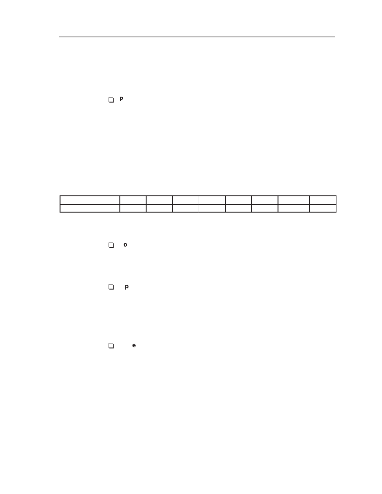
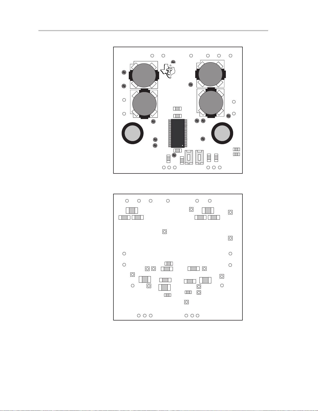
3.10 TPA005D12 Class-D EVM PCB Layers
The following illustrations depict the TP A005D12 class-D EVM PCB assembly
and layers. These drawings are not to scale. Gerber plots can be obtained from
any TI Sales Office.
Figure 3–19. TPA005D12 Class-D EVM Top Assembly
TPA005D12 Class-D EVM PCB Layers
Figure 3–20. TPA005D12 Class-D EVM Bottom Assembly
Details
3-27
Page 42

TPA005D12 Class-D EVM PCB Layers
Figure 3–21. TPA005D12 Class-D EVM Top Layer
Figure 3–22. TPA005D12 Class-D EVM Second Layer
3-28
Details
Page 43

Figure 3–23. TPA005D12 Class-D EVM Third Layer
TPA005D12 Class-D EVM PCB Layers
Figure 3–24. TPA005D12 Class-D EVM Bottom Layer
Details
3-29
Page 44

3-30
Details
 Loading...