

Page 1
TPA005D02 Class D Stereo
Audio Power Amplifier
Evaluation Module
User’s Guide
October 1998 Mixed-Signal Products
SLOU032A
Page 2

IMPORTANT NOTICE
T exas Instruments and its subsidiaries (TI) reserve the right to make changes to their products or to discontinue
any product or service without notice, and advise customers to obtain the latest version of relevant information
to verify, before placing orders, that information being relied on is current and complete. All products are sold
subject to the terms and conditions of sale supplied at the time of order acknowledgement, including those
pertaining to warranty, patent infringement, and limitation of liability.
TI warrants performance of its semiconductor products to the specifications applicable at the time of sale in
accordance with TI’s standard warranty. Testing and other quality control techniques are utilized to the extent
TI deems necessary to support this warranty . Specific testing of all parameters of each device is not necessarily
performed, except those mandated by government requirements.
CERT AIN APPLICATIONS USING SEMICONDUCTOR PRODUCTS MAY INVOLVE POTENTIAL RISKS OF
DEATH, PERSONAL INJURY, OR SEVERE PROPERTY OR ENVIRONMENTAL DAMAGE (“CRITICAL
APPLICATIONS”). TI SEMICONDUCTOR PRODUCTS ARE NOT DESIGNED, AUTHORIZED, OR
WARRANTED TO BE SUITABLE FOR USE IN LIFE-SUPPORT DEVICES OR SYSTEMS OR OTHER
CRITICAL APPLICA TIONS. INCLUSION OF TI PRODUCTS IN SUCH APPLICATIONS IS UNDERST OOD TO
BE FULLY AT THE CUSTOMER’S RISK.
In order to minimize risks associated with the customer’s applications, adequate design and operating
safeguards must be provided by the customer to minimize inherent or procedural hazards.
TI assumes no liability for applications assistance or customer product design. TI does not warrant or represent
that any license, either express or implied, is granted under any patent right, copyright, mask work right, or other
intellectual property right of TI covering or relating to any combination, machine, or process in which such
semiconductor products or services might be or are used. TI’s publication of information regarding any third
party’s products or services does not constitute TI’s approval, warranty or endorsement thereof.
Copyright 1998, Texas Instruments Incorporated
Page 3

Related Documentation From Texas Instruments
J
TI Plug-N-Play Audio Amplifier Evaluation Platform
number SLOU011) provides detailed information on the evaluation
platform and its use with TI audio evaluation modules.
J
TPA005D02 CLASS D STEREO AUDIO POWER AMPLIFIER
(literature number SLOS227) This is the data sheet for the
TPA005D02 audio amplifier integrated circuit.
FCC Warning
This equipment is intended for use in a laboratory test environment only. It
generates, uses, and can radiate radio frequency energy and has not been
tested for compliance with the limits of computing devices pursuant to subpart
J of part 15 of FCC rules, which are designed to provide reasonable protection
against radio frequency interference. Operation of this equipment in other
environments may cause interference with radio communications, in which
case the user at his own expense will be required to take whatever measures
may be required to correct this interference.
Preface
(literature
Trademarks
TI is a trademark of Texas Instruments Incorporated.
Chapter Title—Attribute Reference
iii
Page 4

iv
Page 5

Running Title—Attribute Reference
Contents
1 Introduction 1-1. . . . . . . . . . . . . . . . . . . . . . . . . . . . . . . . . . . . . . . . . . . . . . . . . . . . . . . . . . . . . . . . . . . . .
1.1 Feature Highlights 1-2. . . . . . . . . . . . . . . . . . . . . . . . . . . . . . . . . . . . . . . . . . . . . . . . . . . . . . . . . .
1.2 Description 1-3. . . . . . . . . . . . . . . . . . . . . . . . . . . . . . . . . . . . . . . . . . . . . . . . . . . . . . . . . . . . . . . .
1.3 TP A0202 EVM Specifications 1-4. . . . . . . . . . . . . . . . . . . . . . . . . . . . . . . . . . . . . . . . . . . . . . . .
2 Quick Start 2-1. . . . . . . . . . . . . . . . . . . . . . . . . . . . . . . . . . . . . . . . . . . . . . . . . . . . . . . . . . . . . . . . . . . . . .
2.1 Precautions 2-2. . . . . . . . . . . . . . . . . . . . . . . . . . . . . . . . . . . . . . . . . . . . . . . . . . . . . . . . . . . . . . . .
2.2 Quick Start List for Platform 2-3. . . . . . . . . . . . . . . . . . . . . . . . . . . . . . . . . . . . . . . . . . . . . . . . . .
2.3 Quick Start List for Stand-Alone 2-4. . . . . . . . . . . . . . . . . . . . . . . . . . . . . . . . . . . . . . . . . . . . . .
3 Details 3-1. . . . . . . . . . . . . . . . . . . . . . . . . . . . . . . . . . . . . . . . . . . . . . . . . . . . . . . . . . . . . . . . . . . . . . . . . .
3.1 Precautions 3-2. . . . . . . . . . . . . . . . . . . . . . . . . . . . . . . . . . . . . . . . . . . . . . . . . . . . . . . . . . . . . . . .
3.2 The TPA005D02 Audio Power Amplifier Evaluation Module 3-3. . . . . . . . . . . . . . . . . . . . . .
3.2.1 TPA005D02 Class D Stereo Audio Amplifier IC 3-4. . . . . . . . . . . . . . . . . . . . . . . . . .
3.2.2 Overview of Class D Audio Amplifiers 3-5. . . . . . . . . . . . . . . . . . . . . . . . . . . . . . . . . .
3.2.3 EVM Design Considerations 3-7. . . . . . . . . . . . . . . . . . . . . . . . . . . . . . . . . . . . . . . . . .
3.2.4 Efficiency of Class D vs. Linear Operation 3-15. . . . . . . . . . . . . . . . . . . . . . . . . . . . .
3.3 Using The TPA005D02 Class D EVM With the Plug-N-Play Platform 3-22. . . . . . . . . . . . .
3.3.1 Installing and Removing EVM Boards 3-22. . . . . . . . . . . . . . . . . . . . . . . . . . . . . . . . .
3.3.2 Module Switches 3-23. . . . . . . . . . . . . . . . . . . . . . . . . . . . . . . . . . . . . . . . . . . . . . . . . . .
3.3.3 Signal Routing 3-24. . . . . . . . . . . . . . . . . . . . . . . . . . . . . . . . . . . . . . . . . . . . . . . . . . . . .
3.3.4 Mute 3-25. . . . . . . . . . . . . . . . . . . . . . . . . . . . . . . . . . . . . . . . . . . . . . . . . . . . . . . . . . . . . .
3.3.5 Power Requirements 3-26. . . . . . . . . . . . . . . . . . . . . . . . . . . . . . . . . . . . . . . . . . . . . . . .
3.3.6 Inputs and Outputs 3-27. . . . . . . . . . . . . . . . . . . . . . . . . . . . . . . . . . . . . . . . . . . . . . . . .
3.4 Using The TPA005D02 Class D EVM Stand-Alone 3-28. . . . . . . . . . . . . . . . . . . . . . . . . . . . .
3.4.1 TPA005D02 Class D EVM Connected for BTL Output 3-28. . . . . . . . . . . . . . . . . . .
3.5 TPA005D02 Audio Power Amplifier Evaluation Module Parts List 3-29. . . . . . . . . . . . . . . .
3.6 TPA005D02 Class D EVM Measured Characteristics 3-30. . . . . . . . . . . . . . . . . . . . . . . . . . .
3.7 TPA005D02 Class D EVM PCB Layers 3-33. . . . . . . . . . . . . . . . . . . . . . . . . . . . . . . . . . . . . . .
Chapter Title—Attribute Reference
v
Page 6

Running Title—Attribute Reference
Figures
1–1 The TI TPA005D02 Class D Stereo Audio Amplifier Evaluation Module 1-3. . . . . . . . . . . . . . .
2–1 Quick Start Platform Map 2-2. . . . . . . . . . . . . . . . . . . . . . . . . . . . . . . . . . . . . . . . . . . . . . . . . . . . . .
3–1 The TI Plug-N-Play Audio Amplifier Evaluation Platform 3-2. . . . . . . . . . . . . . . . . . . . . . . . . . . .
3–2 TPA005D02 Class D EVM 3-3. . . . . . . . . . . . . . . . . . . . . . . . . . . . . . . . . . . . . . . . . . . . . . . . . . . . . .
3–3 TPA005D02 Class D EVM Schematic Diagram 3-4. . . . . . . . . . . . . . . . . . . . . . . . . . . . . . . . . . . .
3–4 Class D Functional Diagram 3-5. . . . . . . . . . . . . . . . . . . . . . . . . . . . . . . . . . . . . . . . . . . . . . . . . . . .
3–5 Class D Input and Output Waveforms 3-5. . . . . . . . . . . . . . . . . . . . . . . . . . . . . . . . . . . . . . . . . . . .
3–6 Single-Ended Class D Output FIlter 3-8. . . . . . . . . . . . . . . . . . . . . . . . . . . . . . . . . . . . . . . . . . . . . .
3–7 Low-Pass Filter for Bridged Application 3-9. . . . . . . . . . . . . . . . . . . . . . . . . . . . . . . . . . . . . . . . . .
3–8 Resulting Bridged Output Filter 3-10. . . . . . . . . . . . . . . . . . . . . . . . . . . . . . . . . . . . . . . . . . . . . . . .
3–9 Half-Bridge Class D Output Stage 3-15. . . . . . . . . . . . . . . . . . . . . . . . . . . . . . . . . . . . . . . . . . . . . .
3–10 Class D Currents 3-16. . . . . . . . . . . . . . . . . . . . . . . . . . . . . . . . . . . . . . . . . . . . . . . . . . . . . . . . . . . . .
3–11 Class D Voltages 3-16. . . . . . . . . . . . . . . . . . . . . . . . . . . . . . . . . . . . . . . . . . . . . . . . . . . . . . . . . . . . .
3–12 H-Bridge Class D Output Stage 3-17. . . . . . . . . . . . . . . . . . . . . . . . . . . . . . . . . . . . . . . . . . . . . . . .
3–13 Output Transistor Simplification for Conduction Loss Calculation 3-18. . . . . . . . . . . . . . . . . . .
3–14 Output Switching Losses 3-19. . . . . . . . . . . . . . . . . . . . . . . . . . . . . . . . . . . . . . . . . . . . . . . . . . . . . .
3–15 Audio Signal Showing Peak and RMS Power 3-20. . . . . . . . . . . . . . . . . . . . . . . . . . . . . . . . . . . .
3–16 Audio Signal Showing Peak and RMS Power (with Music Applied) 3-20. . . . . . . . . . . . . . . . . .
3–17 Supply Current vs Peak Output Voltage of TPA005D02 vs TPA0202 with Music Input 3-21.
3–18 Platform Signal Routing and Outputs 3-24. . . . . . . . . . . . . . . . . . . . . . . . . . . . . . . . . . . . . . . . . . .
3–19 Mute/Mode and Polarity Control 3-25. . . . . . . . . . . . . . . . . . . . . . . . . . . . . . . . . . . . . . . . . . . . . . . .
3–20 Typical Headphone Plug 3-27. . . . . . . . . . . . . . . . . . . . . . . . . . . . . . . . . . . . . . . . . . . . . . . . . . . . . .
3–21. TPA005D02 Class D EVM Connected for Stereo BTL Output 3-28. . . . . . . . . . . . . . . . . . . . . . . .
3–22. Frequency Response 3-30. . . . . . . . . . . . . . . . . . . . . . . . . . . . . . . . . . . . . . . . . . . . . . . . . . . . . . . . . .
3–23. Distortion versus Output Power 3-31. . . . . . . . . . . . . . . . . . . . . . . . . . . . . . . . . . . . . . . . . . . . . . . . . .
3–24. Distortion versus Frequency 3-32. . . . . . . . . . . . . . . . . . . . . . . . . . . . . . . . . . . . . . . . . . . . . . . . . . . .
3–25. Crosstalk versus Frequency 3-32. . . . . . . . . . . . . . . . . . . . . . . . . . . . . . . . . . . . . . . . . . . . . . . . . . . . .
3–26. TPA005D02 Class D EVM Silkscreen 3-33. . . . . . . . . . . . . . . . . . . . . . . . . . . . . . . . . . . . . . . . . . . .
3–27. TPA005D02 Class D EVM Top Layer 3-33. . . . . . . . . . . . . . . . . . . . . . . . . . . . . . . . . . . . . . . . . . . . .
3–28. TPA005D02 Class D EVM 2nd Layer 3-34. . . . . . . . . . . . . . . . . . . . . . . . . . . . . . . . . . . . . . . . . . . . .
3–29. TPA005D02 Class D EVM 3rd Layer 3-34. . . . . . . . . . . . . . . . . . . . . . . . . . . . . . . . . . . . . . . . . . . . .
3–30. TPA005D02 Class D EVM Bottom Layer 3-35. . . . . . . . . . . . . . . . . . . . . . . . . . . . . . . . . . . . . . . . . .
T ables
2–1 Typical TI Plug-N-Play Platform Jumper and Switch Settings for the
2–2 Platform Jumper and Switch Settings for the TPA005D02 2-3. . . . . . . . . . . . . . . . . . . . . . . . . .
3–1 TPA005D02 Class D EVM Fault Indicator Table 3-14. . . . . . . . . . . . . . . . . . . . . . . . . . . . . . . . . .
3–2 Efficiency vs Output Power in 5-V 8-W H-Bridge Systems 3-19. . . . . . . . . . . . . . . . . . . . . . . . .
3–3 TPA005D02 Class D EVM Parts List 3-29. . . . . . . . . . . . . . . . . . . . . . . . . . . . . . . . . . . . . . . . . . . .
vi
TPA005D02 Class D EVM 2-1. . . . . . . . . . . . . . . . . . . . . . . . . . . . . . . . . . . . . . . . . . . . . . . . . . . .
Page 7

Chapter 1
Introduction
This chapter provides an overview of the T exas Instruments (TI) TP A005D02
Class D Stereo Audio Amplifier Evaluation Module (SLOP223). It includes a
list of EVM features, a brief description of the module illustrated with a pictorial
diagram, and a list of EVM specifications.
Topic Page
1.1 Feature Highlights 1–2. . . . . . . . . . . . . . . . . . . . . . . . . . . . . . . . . . . . . . . . . . . .
1.2 Description 1–3. . . . . . . . . . . . . . . . . . . . . . . . . . . . . . . . . . . . . . . . . . . . . . . . . . .
1.3 TP A005D02 Class D EVM Specifications 1–4. . . . . . . . . . . . . . . . . . . . . . . .
Introduction
1-1
Page 8
Feature Highlights
1.1 Feature Highlights
The TI TP A005D02 Class D Stereo Audio Amplifier Evaluation Module and the
TI Plug-N-Play Audio Amplifier Evaluation Platform include the following
features:
-
TPA005D02 Class D Stereo Audio Power Amplifier Evaluation Module
J
J
J
J
J
J
J
-
Quick and Easy Configuration with The TI Plug-N-Play Audio Amplifier
Evaluation Platform
J
External depop circuitry to eliminate turn-on transients in outputs
Dual channel, bridge-tied load (BTL) only operation
5-V operation
2 W per channel output power into 4 Ω at 5 V, BTL
Low current consumption in shutdown/mute mode (400 µA)
Module gain set to 24 dB
High efficiency
Evaluation module is designed to simply plug into the platform,
automatically making all signal, control, and power connections
J
Platform provides flexible power options
J
Jumpers on the platform select power and module control options
J
Switches on the platform route signals
J
Platform provides quick and easy audio input and output connections
-
Platform Power Options
J
External 5-V – 15-V DC VCC supply inputs
J
External regulated VDD supply input
J
Socket for onboard 5 V/3.3 V VDD voltage regulator EVM
J
Onboard overvoltage and reverse polarity power protection
-
Platform Audio Input and Output Connections
J
Left and right RCA phono jack inputs
J
Miniature stereo phone jack input
J
Left and right RCA phono jack outputs
J
Left and right compression speaker terminal outputs
J
Miniature stereo headphone jack output
1-2
Introduction
Page 9
Description
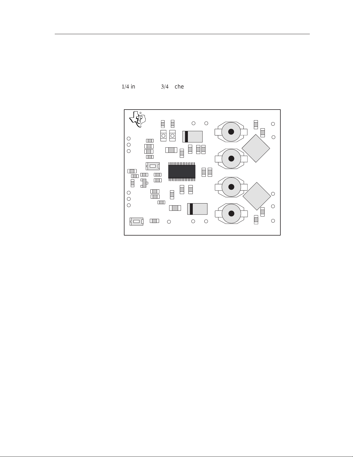
1.2 Description
The TP A005D02 Class D Stereo Audio Power Amplifier Evaluation Module is
a complete, 2-Watt per channel stereo audio power amplifier . It consists of the
TI TPA005D02 Class D Stereo Audio Power Amplifier IC along with a small
number of other parts mounted on a circuit board that measures approximately
2
1/4
inches by 1
Figure 1–1.The TI TPA005D02 Class D Stereo Audio Amplifier Evaluation Module
3/4
inches (Figure 1–1).
GND
RIN+
RIN–
Shutdown
C1
R2
R1
Q1
LIN–
LIN+
GND
Mute
T exas Instruments
R6 R7
1998
C4
C2
C3
C5
R3
R4
R5
D1
S1
SLOP223
C8
S2
C6
C7
D2
1
C10
VDD
GND
C19
C20
L1
C14
L2
C21
L3
U1
L4
GND
D3
+
C12
C13
C9
C17
C15
+
C11
VDD
TPA005D02 EVM Board Rev. A
C24
C23
C25
C26
C22
C27
Rout+
Rout–
Mute
Lout–
Lout+
Single in-line header pins extend from the underside of the module circuit
board to allow the EVM to either be plugged into the TI Plug-N-Play Audio Amplifier Evaluation Platform, or to be wired directly into existing circuits and
equipment when used stand-alone.
The platform has room for a single TPA005D02 class D evaluation module and
is a convenient vehicle for demonstrating TI’s audio power amplifier and
related evaluation modules. The EVMs simply plug into the platform, which
automatically provides power to the modules, interconnects them correctly,
and connects them to a versatile array of standard audio input and output jacks
and connectors. Easy-to-use configuration controls allow the platform and
EVMs to quickly model many possible end-equipment configurations.
There is nothing to build, nothing to solder, and nothing but the speakers
included with the platform to hook up.
Introduction
1-3
Page 10

TPA005D02 Class D EVM Specifications
1.3 TPA005D02 Class D EVM Specifications
Supply voltage range, V
Supply current, I
DD
DD
Continuous output power per channel, P
Audio input voltage, V
Load impedance, R
: 0.47 Vpp max. . . . . . . . . . . . . . . . . . . . . . . . . . . . . . . . . . . . . . . . . . . . . . .
I
L
4.5 V to 5.5 V. . . . . . . . . . . . . . . . . . . . . . . . . . . . . . . . . . . . . . . . . . . . . .
2.8 A max. . . . . . . . . . . . . . . . . . . . . . . . . . . . . . . . . . . . . . . . . . . . . . . . . . . . . . . .
:4-Ω BTL, VDD=5 V 2 W. . . . . . . . . . . . . . . . . . . . . .
O
4 Ω. . . . . . . . . . . . . . . . . . . . . . . . . . . . . . . . . . . . . . . . . . . . . . . . . . . . . . . . . . . .
1-4
Introduction
Page 11

Chapter 2
Quick Start
Follow the steps in this chapter to quickly prepare the TPA005D02 Class D
Stereo Audio Amplifier EVM for use. Using the TP A005D02 class D EVM with
the TI Plug-N-Play Audio Amplifier Evaluation Platform is a quick and easy way
to connect power, signal and control inputs, and signal outputs to the EVM
using standard connectors. However, the audio amplifier evaluation module
can be used stand-alone by making connections directly to the module pins,
and it can be wired directly into existing circuits or equipment.
The platform switch and jumper settings shown in T able 2–1 are typical for the
TPA005D02 class D EVM.
Table 2–1. Typical TI Plug-N-Play Platform Jumper and Switch Settings for the
TPA005D02 Class D EVM
EVM JP6 JP7 JP8 S2 S3
P-N-P Platform Mute X Lo Note 2 U5
Notes: 1) X = Don’t care
2) Set S2 to ON when signal conditioning board is installed in U1; set S2
to OFF when no signal conditioning board is installed.
T opic Page
2.1 Precautions 2–2. . . . . . . . . . . . . . . . . . . . . . . . . . . . . . . . . . . . . . . . . . . . . . . . . .
2.2 Quick Start List for Platform 2–3. . . . . . . . . . . . . . . . . . . . . . . . . . . . . . . . . . .
2.3 Quick Start List for Stand-Alone 2–5. . . . . . . . . . . . . . . . . . . . . . . . . . . . . . . .
Quick Start
2-1
Page 12
Precautions
2.1 Precautions
Power Supply Input Polarity and Maximum Voltage
Always ensure that the polarity and voltage of the external power
connected to V
input connector J6 are correct. Overvoltage or reverse-polarity
power input connector J1, J2, and/or VDD power
CC
power applied to these terminals can open onboard soldered-in
fuses and cause other damage to the platform, installed evaluation
modules, and/or the power source.
Inserting or Removing EVM Boards
Do not insert or remove EVM boards with power applied — damage
to the EVM board, the platform, or both may result.
Figure 2–1.
VCC
In
+
Audio
Input
9
AC/DC
In
Power
Input
7b
Quick Start Platform Map
7b
JP3
JP2
JP1
SOURCE
DC
VCC(J1)
J1
D4
J2
D3
Right
J3
In
Stereo
J4
In
Left
J5
In
TEXAS
INSTRUMENTS
1997
AC/DC
(J2)
D2
Signal Conditioning
Plug-N-Play Audio Amplifier
Evaluation Platform
SLOP097 Rev. C.1
F1
Batt
VR1
D1
LED1
VCC
****CAUTION****
Do not insert or remove
EVM boards with power
applied
C1+
R1
U1
117
Off Pwr
GND
On
S1
Audio
Power
Amps
OnOff
ConditioningS2
TP1
ICC
JP4
B1
IDD
U5
JP5
7b
U3 U4
R2
U2-U4
U5
HP
Source
SUPPLY
U2
HP(U5)
Polarity
S3
R3
R4
7b
POWER
U6
LED2
VDD
JP6
Lo
Hi
JP7
JP8
+
+
F2
J7
Right
Out
J8
+–+–
Right
Out
Left
Out
Mode
Mute
Spk(U2-U4)
J9
Left
Out
Stereo
C3 C2
HP Out
VR2
In/Out
VDD
J10
R5
DC
Power
In/Out
+
J6
Speaker
Output
Headphone
Output
7a
10
5
2-2
3
2
6
4
Quick Start
Page 13
2.2 Quick Start List for Platform
Follow these steps when using the TP A005D02 class D EVM with the TI PlugN-Play Audio Amplifier Evaluation Platform (see the platform user’s guide,
SLOU011, for additional details). Numbered callouts for selected steps are
shown in Figure 2–1 and details appear in Chapter 3.
-
Platform Preparations
Quick Start List for Platform
1) Ensure that all external power sources are set to
power switch S1 is set to
OFF.
2) Install a TP A005D02 module in platform socket U2, taking care to align the
module pins correctly.
3) Use switch S2 to select or bypass the signal conditioning EVM (U1).
4) Set control signal Polarity jumper JP8 to
5) Set jumper JP6 to select the
Mute
control input (causes the TP A005D02
Lo.
to mute if a plug is inserted into platform headphone jack J10).
U5
6) Set switch S3 to
. It is important that S3 always be in the U5 position
to avoid possible damage to the EVM and headphones when the
TPA005D02 class D EVM is installed in platform socket U2.
Table 2–2. Platform Jumper and Switch Settings for the TPA005D02
EVM JP6 JP7 JP8 S2 S3
P-N-P Platform Mute X Lo Note 2 U5
Notes: 1) X = Don’t care
ON
2) Set S2 to
to
OFF
-
Power supply
7) Select and connect the power supply (ensure power supply is set to
a) Connect an external regulated power supply set to 5 V to platform V
power input connector J6 taking care to observe marked polarity,
or
b) Install a voltage regulator EVM (SL VP097 or equiv .) in platform socket
U6. Connect a 7 V – 12 V power source to a platform V
J1 or J2 and jumper the appropriate power input (see platform user’s
guide).
when signal conditioning board is installed in U1; set S2
when no signal conditioning board is installed.
OFF
and that the platform
power input
CC
OFF
):
DD
-
Inputs and outputs
8) Ensure that the audio signal source level is set to minimum.
9) Connect the audio source to left and right RCA phono jacks J3 and J5 or
stereo miniature phone jack J4.
10) Connect 4-Ω – 8-Ω speakers (use 4-Ω for best performance) to left and
right RCA jacks J7 and J9 or to stripped wire speaker connectors J8.
-
Power Up
1 1) V erify correct voltage and input polarity and set the external power supply
to
ON.
If VCC and an onboard regulator EVM are used to provide VDD, set
platform power switch S1 to
ON.
Platform LED2 should light indicating the presence of VDD, and the evaluation
modules installed on the platform should begin operation.
12) Adjust the signal source level as needed.
Quick Start
2-3
Page 14

Quick Start List for Stand-Alone
2.3 Quick Start List for Stand-Alone
Follow these steps to use the TPA005D02 class D EVM stand-alone or to
connect it into existing circuits or equipment. Connections to the TP A005D02
module header pins can be made via individual sockets, wire-wrapping, or
soldering to the pins, either on the top or the bottom of the module circuit board.
-
Power supply
1) Ensure that all external power sources are set to
OFF.
2) Connect an external regulated power supply set to 5 V to the module VDD
and GND pins taking care to observe marked polarity. Separate right
channel and left channel VDD supplies can be connected, or a single
supply can be used for both.
-
Inputs and outputs
3) Ensure that audio signal source level adjustments are set to minimum.
4) Connect the audio source to the module RIN+/RIN– and LIN+/LIN– pins,
taking care to observe marked polarity.
5) Connect a control signal to the module MUTE pin, if necessary . The control
signal should be high or floating for normal operation and low to mute the
module.
6) Connect a 4-Ω – 8-Ω speaker (use 4-Ω for best performance) to the
module ROUT+/ROUT– pins and another speaker to the LOUT+/LOUT–
pins, taking care to observe marked polarity.
-
Power-up
7) Verify correct voltage and input polarity and set the external power supply
to
ON.
2-4
The EVM should begin operation.
8) Adjust the signal source level as needed.
Quick Start
Page 15

Chapter 3
Details
This chapter provides details on the TPA005D02 IC, the evaluation module,
and the steps in the Quick-Start List, a discussion on class D amplifiers,
additional application information, a parts list for the TPA005D02 class D
evaluation module, module performance graphs, and module PCB layer
illustrations.
Topic Page
3.1 Precautions 3-2. . . . . . . . . . . . . . . . . . . . . . . . . . . . . . . . . . . . . . . . . . . . . . . . . .
3.2 The TPA005D02 Audio Power Amplifier Evaluation Module 3-3. . . . . . .
3.3 Using The TPA005D02 Class D EVM With the P-N-P Platform 3-22. . . .
3.4 Using The TPA005D02 Class D EVM Stand-Alone 3-28. . . . . . . . . . . . . . .
3.5 TP A005D02 Audio Power Amplifier Evaluation Module Parts List 3-29
3.6 TP A005D02 Class D EVM Measured Characteristics 3-30. . . . . . . . . . . . .
3.7 TP A005D02 Class D EVM PCB Layers 3-33. . . . . . . . . . . . . . . . . . . . . . . . . .
Details
3-1
Page 16
Precautions
3.1 Precautions
Power Supply Input Polarity and Maximum Voltage
Always ensure that the polarity and voltage of the external power
connected to V
input connector J6 are correct. Overvoltage or reverse-polarity
power applied to these terminals can open onboard soldered-in
fuses and cause other damage to the platform, installed evaluation
modules, and/or the power source.
Inserting or Removing EVM Boards
Do not insert or remove EVM boards with power applied — damage
to the EVM board, the platform, or both may result.
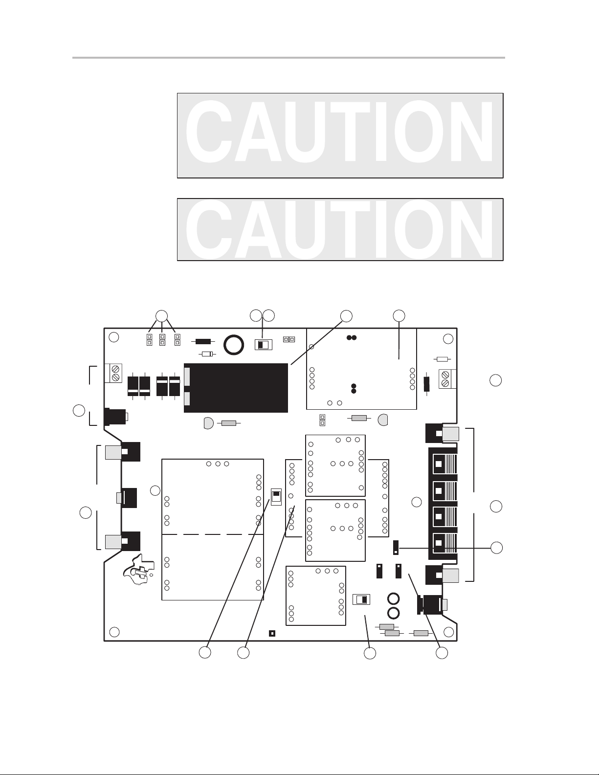
Figure 3–1.The TI Plug-N-Play Audio Amplifier Evaluation Platform
Power
Input
Audio
Input
In
+
AC/DC
In
VCC
D4
J2
In
In
In
J1
SOURCE
DC
VCC(J1)
D3
Right
J3
Stereo
J4
Left
J5
JP1
JP3
AC/DC
(J2)
D2
JP2
D1
Batt
VR1
F1
VCC
LED1
Signal Conditioning
C1+
R1
U1
power input connector J1, J2, and/or VDD power
CC
On
Off Pwr
S1
ICC
JP4
SUPPLY
POWER
B1
JP5
IDD
LED2
VDD
R2
Audio
Power
Amps
U3 U4
U2
OnOff
ConditioningS2
U6
J7
Out
Out
Out
VR2
F2
DC
Power
In/Out
+
J6
In/Out
VDD
Right
J8
+–+–
Right
Speaker
Output
Left
3-2
TEXAS
INSTRUMENTS
1997
Plug-N-Play Audio Amplifier
Evaluation Platform
SLOP097 Rev. C.1
****CAUTION****
Do not insert or remove
EVM boards with power
applied
GND
TP1
U5
U2-U4
U5
HP
Source
HP(U5)
S3
R3
R4
JP6
Polarity
Lo
Hi
JP7
+
+
Mode
Mute
Spk(U2-U4)
Out
JP8
C3 C2
HP Out
J9
Left
Stereo
Headphone
Output
J10
R5
Details
Page 17
The TPA005D02 Audio Power Amplifier Evaluation Module
3.2 The TPA005D02 Audio Power Amplifier Evaluation Module
The TP A005D02 Class D Stereo Audio Power Amplifier Evaluation Module is
powered by a TPA005D02 class D stereo power amplifier integrated circuit
capable of delivering greater than 2 W of continuous power per channel into
4-Ω loads. The amplifier IC operates in the bridge-tied load mode for maximum
efficiency. The evaluation module includes onboard switches for muting and
shutdown and a control input pin for muting. A pair of indicator LEDs are
mounted on the module to display power supply undervoltage and amplifier
IC thermal status.
The module can be used with the TI Plug-N-Play Audio Amplifier Evaluation
Platform (Figure 3–1) or wired directly into circuits or equipment. The module
has single in-line header connector pins mounted to the underside of the
board. These pins allow the module to be plugged into the TI platform, which
automatically makes all the signal input and output, power, and control
connections to the module.
The module connection pins are on 0.1-inch centers to allow easy use with
standard perf board and plug board-based prototyping systems. Or, the EVM
can be wired directly into existing circuits and equipment when used
stand-alone.
The module appears in Figure 3–2 and its schematic is shown in Figure 3–3.
Figure 3–2.TPA005D02 Class D EVM
T exas Instruments
R6 R7
1998
GND
RIN+
RIN–
Shutdown
C1
R2
R1
Q1
LIN–
LIN+
GND
Mute
R3
C4
C2
C3
C5
R4
R5
D1
S1
SLOP223
C8
S2
C6
C7
D2
1
C10
VDD
GND
C19
C20
L1
C14
L2
C21
L3
U1
L4
GND
D3
+
C12
C13
C9
C17
C15
+
C11
VDD
TPA005D02 EVM Board Rev. A
C24
C23
C25
C26
C22
C27
Rout+
Rout–
Mute
Lout–
Lout+
Details
3-3
Page 18

The TPA005D02 Audio Power Amplifier Evaluation Module
Figure 3–3.TPA005D02 Class D EVM Schematic Diagram
V
V
GND
GND
MUTE
LIN+
LIN–
RIN+
RIN–
DD
DD
R5
100 KΩ
R1
20 KΩ
V
DD
Mute
C21
0.047 µF
C20
0.047 µF
V
DD
C1
1 µF
R2
1 KΩ
R3
D1
20 KΩ
3.9 V
S2
1 µF
C6
470 pF
C8
C2
1 µF
C3
470 pF
C4
470 pF
C5
C19
1 µF
1 µFC7
1 µF
Q1
2N3906
Shutdown
S1
1
2
3
5
4
6
7
44
45
43
17
19
30
48
47
46
20
22
28
26
23
24
25
100 KΩ
SHUTDOWN
MUTE
AGND
LINP
LINN
LCOMP
AGND
RINP
RINN
RCOMP
NC
NC
NC
COSC
AGND
AGND
AGND
VCP
LSBIAS
CP4
CP3
CP2
CP1
PowerPAD
R4
U1
TPA005D02
LPV
DD
LPV
DD
V
DD
PV
DD
RPV
DD
RPV
DD
PV
DD
FAULT0
FAULT1
LOUTP
LOUTP
PGND
PGND
LOUTN
LOUTN
ROUTP
ROUTP
PGND
PGND
ROUTN
ROUTN
NC
NC
V2P5
PGND
C13
1 µ
F
9
16
8
21
40
33
32
42
L4
µH
15
L3
15
µH
L1
15 µH
L2
15 µH
D3
C18
1 µF
41
10
11
12
13
14
15
39
38
37
36
35
34
18
31
29
27
C9
1 µF
C26
0.22 µF
C17
1 µF
C25
0.22 µF
0.22 µF
C24
0.22 µF
C27
+
F
F
µ
10
D2
R7
C23
1 µF
C22
1 µF
µ
220
R6
1 KΩ
F
1 µ
1 KΩ
LOUT+
LOUT–
ROUT+
ROUT–
F
1 µ
C16
C12
C14
C10
V
DD
C11
C15
+
F
F
µ
µ
10
220
V
DD
3.2.1 TPA005D02 Class D Stereo Audio Amplifier IC
The TPA005D02 Class D Stereo Audio Power Amplifier integrated circuit
converts low-level audio into pulse-width-modulated (PWM) signals, which
result in an audio output with a 24-dB increase in amplitude. Designed
primarily for BTL operation at a supply voltage of 5 V, each channel of the
TP A005D02 amplifier IC is capable of 2 W of continuous output power into a
4-Ω load at 0.8% total harmonic distortion + noise (THD+N) over a frequency
range of 20Hz – 20kHz.
The device is provided in a very small 48-pin thermally-enhanced PowerP AD
TSSOP surface-mount package (DCA) and consumes only 400 µA in
shutdown mode, making the TPA005D02 an excellent choice for portable
battery-powered applications.
3-4
Details
Page 19

The TPA005D02 Audio Power Amplifier Evaluation Module
3.2.2 Overview of Class D Audio Amplifiers
Class D audio amplifiers are very similar in operation to switch-mode power
supplies in that both compare an input signal with a reference to create an error
voltage that controls a pulse-width modulator (PWM) circuit. The PWM then
produces an output signal at constant frequency and with a duty cycle that
varies according to the input signal. This controls the switching action of the
output power stage (H-bridge). A block diagram of the major components that
make up the amplifier is shown in Figure 3–4.
Figure 3–4.Class D Functional Diagram
Audio
Analog
Source
Ramp
Generator
Comparator
V
ERROR
The audio input signal (Vin) is applied to a comparator along with a triangle
wave created by the ramp generator (V
the audio input on the rising and falling ramps, the comparator sends an error
signal to the PWM control circuit. The PWM signal regulates the duty cycle of
the H-bridge circuit to provide V
in Figure 3–5.
Figure 3–5.Class D Input and Output Waveforms
V
PWM
Control
LPF
ramp
. Examples of these waveforms are shown
out
CONTROL
V
OUT
H-Bridge
Load
). When the triangle wave crosses
V
IN
V
RAMP
5 V
V
OUT
0 V
The triangle wave must be operating at a much higher frequency than the
highest frequency component of the input signal in order to get an accurate
representation at the amplifier output. The TP A005D02 EVM uses a 250 kHz
switching rate to sample the input, which is more than ten times higher than
the highest frequency component of the 20 Hz to 20kHz audio input range.
Details
3-5
Page 20

The TPA005D02 Audio Power Amplifier Evaluation Module
The H-bridge circuit consists of DMOS power transistors for supplying the
heavy currents which are required by the load. These transistors operate in
either the cutoff or saturation regions rather than the linear region in which
class AB amplifiers operate. Switching and conduction losses are reduced
since the transistor is active for only a small part of the duty cycle, reducing the
power dissipated by the power transistors and allowing more power to be
delivered to the load. A low pass filter (LPF) then removes the high frequency
switching component from the output signal, leaving an amplified version of
the original input signal. The DMOS transistors are arranged in an H-bridge
(full bridge) configuration to allow BTL operation, which further enhances the
amplifier performance.
3.2.2.1 BTL Operation
In the bridge-tied load output mode, the two output lines of each channel
operate as mirror images of each other for increased power. The speaker load
is connected directly across OUT+ and OUT–, and neither line is connected
to ground. BTL operation provides many benefits, including quadruple the
output power of single-ended operation and no need for bulky output coupling
capacitors. For more information, see the TP A005D02 amplifier IC data sheet,
TI Literature Number SLOS205.
T o operate in the bridge-tied load output mode, the module output signal from
OUT+ must go through the speaker load and be returned directly to OUT–, and
NOT
to system ground. This requires that the OUT– line be isolated not only
from system ground, but also from the OUT– lines of any other amplifiers in
the system. The platform provides such isolated output lines from the amplifier
EVM sockets directly to separate left and right speaker connectors.
3-6
Details
Page 21

3.2.3 EVM Design Considerations
Circuit design and layout plays a large role in the creation or reduction of
distortion in class D amplifiers, and the high frequency switching
characteristics of class D audio power amplifier output stages offer some
interesting design challenges over conventional class AB amplifiers.
The main goal of the design of this EVM is to offer the best performance with
the smallest components, without sacrificing performance. For this reason
surface mount technology (SMT) parts are used whenever possible. The
major design considerations are discussed below and refer to Figures 3–2 and
3–3 unless otherwise noted. The actual parts used in the EVM are listed in
Table 3–3.
The audio signal path is the most critical, so the discussion begins there.
3.2.3.1 Input Filter
The first consideration is the desired frequency bandwidth (BW). High-fidelity
audio requires a flat 20Hz to 20kHz bandwidth. The low frequency –3-dB point
is set using an ac coupling capacitor at the amplifier inputs (IC pins 4, 5, 44,
and 45) which creates a high-pass filter (HPF). The –3-dB point for a first-order
HPF is found using the equation
The TPA005D02 Audio Power Amplifier Evaluation Module
1
+
f
LO
(2pRC)
where R = 10 kΩ is the input resistance of the amplifier and C = 1 µF for the
value of capacitors C2, C3, C6, and C7. These values give a –3-dB point of
15.9 Hz—close to the desired –3-dB point of 20 Hz. Ceramic capacitors are
preferred over electrolytic for their small size, low equivalent series resistance
(ESR), low noise, and long life. The smallest ceramic SMT package currently
available is 0603, yet availability necessitates using an 0805 package.
Other considerations are stability over temperature, voltage rating, and cost.
A tradeoff exists between the size, temperature characteristics, rated voltage,
and capacitance value. For a given package size, for example, an increase in
the voltage rating means a decrease in capacitance. The same applies to
improved temperature stability.
Temperature stability has little impact on the input capacitors since they
primarily couple the ac input signal and are not expected to dissipate large
amounts of heat. The input voltage is low for the class D EVM (less than
0.5 Vrms), so the rated voltage can also be low. An 0805 SMT package with
a rated voltage of 5 V and Y5V temperature characteristics would be ideal for
this application. Availability and cost constraints, however , dictated the use of
the power supply bypass capacitors that were finally selected, which meet all
requirements and are rated at 16V. If better matching of the left and right
channels is needed or a harsh environment will be encountered, then a
capacitor with X7R temperature characteristics should be considered.
Details
3-7
Page 22

The TPA005D02 Audio Power Amplifier Evaluation Module
3.2.3.2 Output Filter
Class D amplifiers require special filtering at the output to remove the
high-frequency switching component and accurately reconstruct the audio
signal. The output filter is a low-pass filter (LPF) which sets the high frequency
–3-dB point of the bandwidth. The major consideration here is how to choose
the components and set the desired –3-dB point.
Filter Design Goals
A second-order low-pass filter is used for the output filter. The Butterworth filter
is characterized by a flat response over the pass band and less attenuation
after the cutoff frequency. The order of the filter determines how many poles
exist that are at the same frequency, with each pole providing –20 dB per
decade of signal attenuation for a total of –40 dB per decade in this circuit. The
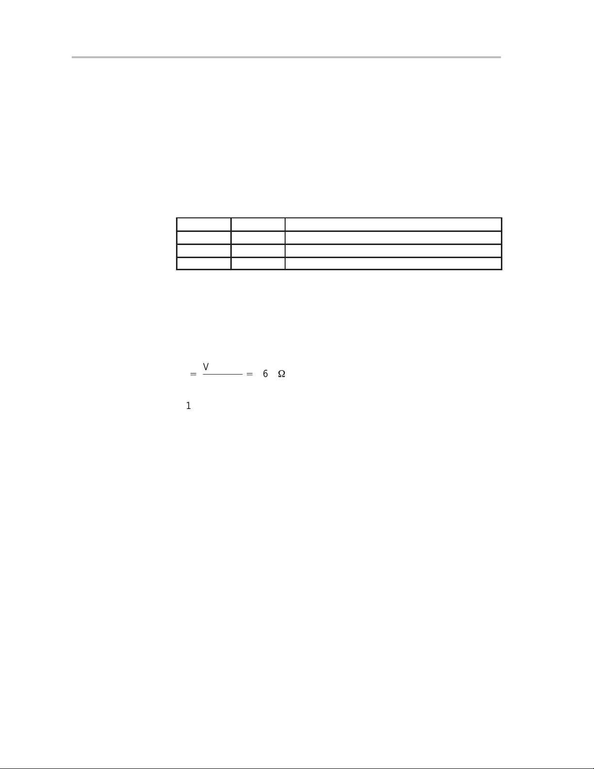
cutoff frequency (fc) can be determined using the equation
f
+
C
1
Ǹ
(2pLC
)
where L is the inductance and C is the equivalent capacitance. The values
used in the output filter are 15 µH for the inductor, and 0.22 µF and 1 µF
capacitors in parallel for an equivalent capacitance of 2.22 µF, setting the
cutoff frequency to 27.5 kHz. The main purpose of this filter is to reduce the
switching frequency to an acceptable level and not attenuate the audio band.
The 250 kHz amplifier output signal is then reduced by –40 dB to one percent
of its pre-filter value.
The considerations for inductor selection are inductance, continuous and peak
current ratings, dc series resistance, and the packaging. The inductance was
chosen based on common inductance and capacitance values, to be 15 µH.
Class D Output Filter Design Methodology
The output filter attenuates the high switching frequency. A second-order
Butterworth low-pass filter was chosen for its flat pass band, good phase
response, and low parts count (it requires only an inductor and a capacitor).
The normalized transfer for the Butterworth filter is
H(s)
+
s2)
1
Ǹ
2
s)1
The next step is to realize the circuit and develop a transfer function. The filter
for a single-ended application is shown in Figure 3–6.
Figure 3–6.Single-Ended Class D Output FIlter
I
L
L
3-8
+
V
I
–
I
O
+
R
V
L
C
L
O
–
Details
Page 23

The TPA005D02 Audio Power Amplifier Evaluation Module
The transfer function is easily derived by using a voltage divider equation with
the load voltage being a parallel combination of R
and CL. This transfer
L
function is
1
1
RLC
LC
S)
L
L
1
LC
L
VO(s)
VI(s)
+
S2)
The next step is to set the terms of the circuit transfer function equal to the
terms of the normalized 2nd-order Butterworth low-pass filter and solve for L
and C
CL+
in terms of RL. This yields
L
1
Ǹ
2
R
L
L
+
2Ǹ
R
L
These values give a cut-off frequency at ω
that the components must be frequency scaled. To frequency scale, each
component is divided by ω
= 2 × π × f
0
Hertz):
CSE+
LSE+
ω0+2 p
1
Ǹ
2
RL
ω
0
Ǹ
R
2
L
w
o
f
c
Because the TP A005D02 is a bridged amplifier, this filter is needed at both the
positive and negative output. This means that R
filter, so for a bridged application, R
calculations. One capacitor can be used in place of the two capacitors in the
output filters if the capacitor is placed across R
to ground. This circuit is shown in Figure 3–7.
R
L
Figure 3–7.Low-Pass Filter for Bridged Application
I
O
+ VO –
+
–
L
BTL
V
I
= 1 radian/second, which means
0
(fc is the desired cut-off frequency in
c
must be split between each
L
must be divided by 2 in the component
L
instead of from each side of
L
R
C
L
BTL
+
V
I
–
Details
3-9
Page 24

The TPA005D02 Audio Power Amplifier Evaluation Module
The component equations adjusted for bridged amplifiers are
C
L
BTL
BTL
+
Ǹ
+
Ǹ
2
2
2 ω
1
RL
R
L
0
T o find component values, let fc = 30 kHz, which yields ω0 = 188495.6 radians/
second. If a 4-Ω speaker is used, R
= 0.94 µF . Additional capacitors can be added from each side of RL to ground
to provide a high-frequency short to ground. These additional capacitors
should be approximately 10% of 2C
Figure 3–8 with the components rounded to standard values.
Figure 3–8.Resulting Bridged Output Filter
LOUTP or ROUTP
LOUTN or ROUTN
ω
0
15 µH
15 µH
= 4 Ω. This yields L
L
. The resulting output filter is shown in
BTL
0.22 µF
1 µF
0.22 µF
= 15 µH and C
BTL
BTL
4 Ω
Output Filter Components
The output inductors are key elements in the performance of the class D audio
amplifier system. It is important that these inductors have a high enough
current rating and a relatively constant inductance over frequency and
temperature. The current rating should be higher than the maximum current
expected to avoid magnetically saturating the inductor. When saturation
occurs, the inductor loses its functionality and looks like a short circuit to the
PWM signal, which increases the harmonic distortion considerably.
A shielded inductor may be required if the class D amplifier is placed in an EMI
sensitive system; however, the switching frequency is low for EMI
considerations and should not be an issue in most systems. The DC series
resistance of the inductor should be low to minimize losses due to power
dissipation in the inductor, which reduces the efficiency of the circuit.
Capacitors are important in attenuating the switching frequency and high
frequency noise, and in supplying some of the current to the load. It is best to
use capacitors with low equivalent-series-resistance (ESR). A low ESR
means that less power is dissipated in the capacitor as it shunts the
high-frequency signals. Ceramic (C24, C25, C26, and C27) and metal film
(C22 and C23) capacitors were selected because of their low ESR. Placing
these capacitors in parallel also parallels their ESR, effectively reducing the
overall ESR value. The voltage rating is also important, and, as a rule of thumb,
should be 2 to 3 times the maximum rms voltage expected to allow for high
peak voltages and transient spikes. These output filter capacitors should be
stable over temperature since large currents flow through them.
3-10
Details
Page 25

3.2.3.3 Power Filtering
The TPA005D02 Audio Power Amplifier Evaluation Module
Power supply considerations include power supply decoupling and high
frequency bypass loops. Electrolytic capacitors are used for decoupling and
ceramic or mica capacitors are used for high frequency bypass applications.
Decoupling capacitors serve to smooth the input voltage and assist the
amplifier by providing current when needed. These capacitors may shunt
relatively large ripple currents to ground and must have a low equivalent series
resistance (ESR) to reduce power and heat dissipation in the device. The ESR
combines all losses, both series and parallel, in a capacitor at a given
frequency in order to reduce the equivalent circuit to a simple RC series
connection, valid only for low frequencies (less than 1 MHz).
Other considerations are the voltage rating, capacitance, physical size, and
the specific type of capacitor. The voltage rating should exceed the maximum
supply voltage expected in order to handle voltage surges and spikes without
being damaged. The capacitance is then important, as it specifies the amount
of energy that can be stored in the capacitor. Once the voltage rating and
capacitance are known, the size can be determined.
Since the focus was to get the largest capacitance possible yet keep the size
to a minimum, tantalum capacitors, instead of aluminum electrolytic
capacitors, were chosen. Tantalum capacitors provide a higher capacitance
value in a smaller package and have lower ESR values than aluminum
electrolytic capacitors. SMT packages further reduce the inductance
associated with lead lengths. All of these considerations led to the selection
of a 220 µF SMT tantalum capacitor as the primary decoupling capacitor.
The high frequency bypass capacitors are usually small in size, limited by the
size of the capacitance to approximately 10 µF or less. Ceramic capacitors
have extremely low ESR and dissipate very little power. Lower ESR means a
lower net impedance at higher frequencies, which is more suitable for filtering
the higher frequency components of the power supply, especially voltage
spikes. Bypass capacitors should be placed as close as possible to the IC
power input pins and also as close to the IC power ground pins as possible.
The idea is to form the smallest possible loop, or path, over which the high
frequency signals can travel, and minimize the impedance. A short path with
a high impedance defeats the purpose.
The power pins (VDD) were placed at the top and bottom of the IC package,
and the power traces and filtering capacitors were arranged to balance the left
and right channels of the IC. A trace along the bottom of the board links the
V
pins for EVM stand-alone operation and supplies power to the right and
DD
left channels in parallel. This places the capacitors and their ESR in parallel,
increasing the overall capacitance seen by the power source while greatly
reducing the ESR.
Details
3-1 1
Page 26

The TPA005D02 Audio Power Amplifier Evaluation Module
3.2.3.4 Ground Plane
Experimentation with several types of ground planes has shown that a solid
ground plane works as well as methods that split the analog and power ground
planes when good layout practices are followed. This allows a much simpler
design that requires less time and is less prone to layout errors. The success
of the solid ground plane is partially due to the TPA005D02 IC, which allows
the designer to keep the input and output sections of the chip separated,
reducing the chance that high- and mid-frequency return currents will make a
path to the analog input section of the chip.
The traces for the analog circuit grounds are extremely short and are
connected to the ground immediately under the chip through vias, while the
power circuit grounds are connected to the ground plane slightly further out
from the chip and closer to the signal outputs and power inputs. The large
current traces of the output are then shielded from the input circuit by the
ground plane.
The solid ground plane has low resistance compared with the narrow paths to
pins and vias that are attached. If a voltage spike or current spike hits the
ground plane, the entire plane shifts up or down, unlike a split plane, which has
inductance between the halves that dampens the noise and can cause uneven
voltage potentials to exist.
3.2.3.5 Compensation, Ramp Generator, and Charge Pump Capacitors
The components (C19, C5, C4 and C8) for these circuits are critical to the
operation of the TP A005D02 amplifier. The capacitance at these nodes must
be close to the specified value and maintain this value over EVM temperature
extremes. Ceramic capacitors with X7R temperature characteristics should be
used for their low ESR and their stability over a wide temperature range. Tight
tolerances are needed, especially for RCOMP (C4) and LCOMP (C8), which
need to track closely for good left and right channel matching. A high voltage
rating is not needed (15 V would work), yet 50 V is one of the lowest ratings
for the size and type of capacitor selected.
Ramp generator capacitor C5 does not need the tight capacitance value
tolerance that C4 and C8 require; however, capacitance stability over
temperature change is important.
Charge pump capacitor C19 has the same requirements as the ramp
generator capacitor (C5), though the size is much larger and the necessary
voltage rating due to the charge tripling is increased, making the part
somewhat less readily available.
3-12
Details
Page 27

3.2.3.6 Control and Indicator Circuits
The shutdown circuit, the mute circuit, and the fault indicator circuit are all
low-current circuits and are not as critical in the layout design as the circuits
mentioned previously.
Shutdown
The shutdown control (IC pin 1) is activated by a logic low. Shutdown limits the
supply current of the TPA005D02 to 400 µA to conserve power in low power
applications.
The shutdown circuit (IC pin 1) consists of D1, Q1, R1, R2, R3, R4, C1, and
S2, a relatively large number of components. Since space and power
consumption are to be minimized, these components need to be small,
low-power devices. Switch S2 is actually the component that sends the device
into shutdown mode—there is no shutdown control input pin on the EVM. The
remaining components form a delay circuit that eliminates noise created by the
discharge of energy stored in the output filter when the amplifier IC is initially
placed in shutdown.
The PNP transistor needs to be biased so that it is operational from at least
4.5 V to 5.5 V. Zener diode D1 and resistors R1, R2, and R3 set the bias for
the transistor so that it is kept in its linear region and minimizes the supply
current used by this circuit. The maximum zener voltage Vz is then calculated
to be
The TPA005D02 Audio Power Amplifier Evaluation Module
Vz = V
DD(min)–VBE(min)
= 4.5V–0.6V = 3.9V
Zener diode D1 was selected based on Vz and the current required for
operation. Resistor R1 limits the current through the diode, while R2 also helps
limit the base current and isolate the bootstrap capacitor C1. Resistor R3 limits
the collector current during normal operation, and R4 limits the current flowing
to ground when switch S2 is closed.
Mute
The mute control (IC pin 2) is activated by a logic low, in which case the
amplifier low-side output transistors are turned on, shorting the load to ground.
The main consideration is to minimize the current used. A 100-kΩ pullup
resistor is used to limit the current to microamps and minimize the power
dissipated in the resistor, allowing a smaller surface-mount package to be
used.
Details
3-13
Page 28
The TPA005D02 Audio Power Amplifier Evaluation Module
Fault Indicator
The TP A005D02 IC has two fault indicator pins (IC pins 41 and 42) to indicate
an under-voltage condition or a thermal fault. When the device is operating
normally, both pins are pulled up to the supply voltage through R6/D2 and
R7/D3. If the power supply voltage drops too low, the charge pump voltage
drops below the operational threshold and the low-side transistors short to
ground. When this occurs, IC pin 41 goes to ground, creating a voltage drop
across the LED, causing it to illuminate. The LED remains lit until the fault
circuit is reset by cycling the power or operating the shutdown or mute switch.
Table 3–1. TPA005D02 Class D EVM Fault Indicator Table
LED 1 LED 2 Fault Description
OFF OFF No faults—device is operating normally
OFF ON Under-voltage condition
ON ON Thermal fault
The fault indicator circuits (IC pins 41 and 42) are designed to minimize current
consumption and yet have an LED that is clearly visible when illuminated. The
LED should be as small as possible, have a wide viewing angle, and be bright
enough to clearly see while using minimal current. The LEDs selected require
a 2.1-V drop when activated, and approximately 3 mA of current to be fully
illuminated. The current-limit resistance needed is then calculated:
+
DD
R
d
+
967
I
d
W
–V
V
A 1-kΩ resistor was used for R6 and R7. Tests demonstrate that the LEDs
selected operate as expected and are clearly visible when the fault circuit is
activated.
3-14
Details
Page 29

The TPA005D02 Audio Power Amplifier Evaluation Module
3.2.4 Efficiency of Class D vs. Linear Operation
Amplifier efficiency is defined as the ratio of output power delivered to the load
to power drawn from the supply . In the efficiency equation below, P
across the load and P
Efficiency+h
A high-efficiency amplifier has a number of advantages over one with lower
efficiency. One of these advantages is a lower power requirement for a given
output, which translates into less waste heat that must be removed from the
device, smaller power supply required, and increased battery life.
Audio power amplifier systems have traditionally used linear amplifiers, which
are well known for being inefficient. Class D amplifiers were developed as a
means to increase the efficiency of audio power amplifier systems.
A linear amplifier is designed to act as a variable resistor network between the
power supply and the load. The transistors operate in their linear region and
voltage that is dropped across the transistors (in their role as variable
resistors) is lost as heat, particularly in the output transistors.
is the supply power.
SUP
P
L
+
P
SUP
is power
L
The output transistors of a class D amplifier switch from full OFF to full ON
(saturated) and then back again, spending very little time in the linear region
in between. As a result, very little power is lost to heat because the transistors
are not operated in their linear region. If the transistors have a low ON
resistance, little voltage is dropped across them, further reducing losses. The
ideal class D amplifier is 100% efficient, which assumes that both the ON
resistance (R
DS(ON)
) and the switching times of the output transistors are zero.
3.2.4.1 The Ideal Class D Amplifier
To illustrate how the output transistors of a class D amplifier operate, a
half-bridge application is examined first (Figure 3–9).
Figure 3–9.Half-Bridge Class D Output Stage
V
DD
M1
V
A
M2
I
L
L
I
OUT
+
V
R
C
L
C
OUT
L
–
Details
3-15
Page 30

The TPA005D02 Audio Power Amplifier Evaluation Module
Figures 3–10 and 3–11 show the currents and voltages of the half-bridge
circuit. When transistor M1 is on and M2 is off, the inductor current is
approximately equal to the supply current. When M2 switches on and M1
switches off, the supply current drops to zero, but the inductor keeps the
inductor current from dropping. The additional inductor current is flowing
through M2 from ground. This means that VA (the voltage at the drain of M2,
as shown in Figure 3–9) transitions between the supply voltage and slightly
below ground. The inductor and capacitor form a low-pass filter, which makes
the output current equal to the average of the inductor current. The low pass
filter averages V
, which makes V
A
by the duty cycle.
Control logic is used to adjust the output power, and both transistors are never
on at the same time. If the output voltage is rising, M1 is on for a longer period
of time than M2.
Figure 3–10. Class D Currents
equal to the supply voltage multiplied
OUT
Current
0
M1 on
M2 off
Figure 3–11. Class D Voltages
Voltage
M1 off
M2 on
M1 on
M2 off
Time
Inductor Current
Output Current
Supply Current
V
V
A
V
OUT
DD
3-16
0
M1 on
M2 off
M1 off
M2 on
M1 on
M2 off
Time
Details
Page 31

The TPA005D02 Audio Power Amplifier Evaluation Module
Given these plots, the efficiency of the class D device can be calculated and
compared to an ideal linear amplifier device. In the derivation below, a sine
wave of peak voltage (V
) is the output from an ideal class D and linear
P
amplifier and the efficiency is calculated.
CLASS D LINEAR
V
AverageǒI
PL+
P
P
SUP
L(rms)
SUP
+
VL
+
VDD
V
+
Ǹ
DD
I
DD
Efficiency+h
P
2
Ǔ
+
L
+
L(rms)
I
V
AverageǒI
I
L(rms)
V
DD
P
L
P
SUP
V
DD
DD
V
L(rms)
Ǔ
L(rms)
V
L(rms)
V
PL+
AverageǒI
P
+
SUP
Efficiency
Efficiency
V
Efficiency+h+1 Efficiency
V
+
Ǹ
L(rms)
R
L
DD
VDD
+h+
+h+
+h+
P
2
2
+
Ǔ
+
2
V
P
2R
L
V
2
P
p
R
L
AverageǒI
P
L
P
SUP
VDD
p
4
V
V
DD
P
DD
V
DDVP
Ǔ
+
R
L
2
V
P
2R
L
V
2
P
p
R
L
2
p
In the ideal efficiency equations, assume that VP = VDD, which is the maximum
sine wave magnitude without clipping. Then, the highest efficiency that a linear
amplifier can have without clipping is 78.5%. A class D amplifier, however , can
ideally have an efficiency of 100% at all power levels.
The derivation above applies to an H-bridge as well as a half-bridge. An
H-bridge requires approximately twice the supply current but only requires half
the supply voltage to achieve the same output power—factors that cancel in
the efficiency calculation. The H-bridge circuit is shown in Figure 3–12.
Figure 3–12. H-Bridge Class D Output Stage
V
DD
M1
V
A
M2
I
I
L
OUT
L
C
L
V
+
OUT
R
L
V
DD
–
C
L
M4
L
M3
Details
3-17
Page 32

The TPA005D02 Audio Power Amplifier Evaluation Module
3.2.4.2 Losses in a Real-World Class D Amplifier
Losses make class D amplifiers nonideal, and reduce the efficiency below
100%. These losses are due to the output transistors having a nonzero
R
, and rise and fall times that are greater than zero.
DS(on)
The loss due to a nonzero R
is called conduction loss, and is the power
DS(on)
lost in the output transistors at nonswitching times, when the transistor is ON
(saturated). Any R
above 0 Ω causes conduction loss. Figure 3–13
DS(on)
shows an H-bridge output circuit simplified for conduction loss analysis and
can be used to determine new efficiencies with conduction losses included.
Figure 3–13. Output Transistor Simplification for Conduction Loss Calculation
VDD = 5 V
R
DS(on)
R
DS(off)
The power supplied, P
plus the power lost in the transistors, assuming that there are always two
transistors on.
0.31 Ω
5 MΩ
SUP
5 MΩ
R
L
4 Ω
0.31 Ω
, is determined to be the power output to the load
R
DS(off)
R
DS(on)
Efficiency
Efficiency
Efficiency
Efficiency
Efficiency
+h+
+h+
+h+
+h+
+h+
P
L
P
SUP
2
R
I
L
I22R
2R
DS(on)
DS(on)
)
I2R
L
R
L
)
R
L
95%ǒat all output levels R
87%ǒat all output levels R
DS(on)
DS(on)
+
0.1, RL+
+
0.31, RL+
Ǔ
4
Ǔ
4
3-18
Details
Page 33

Losses due to rise and fall times are called switching losses. A plot of the
output, showing switching losses, is shown in Figure 3–14.
Figure 3–14. Output Switching Losses
The TPA005D02 Audio Power Amplifier Evaluation Module
1
f
SW
t
SWon
+
Rise and fall times are greater than zero for several reasons. One is that the
output transistors cannot switch instantaneously because (assuming a
MOSFET) the channel from drain to source requires a specific period of time
to form. Another is that transistor gate-source capacitance and parasitic
resistance in traces form RC time constants that also increase rise and fall
times.
The switching power loss formula below with the following values (V
t
= 50 ns, fSW = 250 kHz, R
SW
loss of 4.4 mW at all output powers.
1
tSW
2
P
+
SW
Switching losses are constant at all output power levels, which means that
switching losses can be ignored at high power levels in most cases. At low
power levels, however, switching losses must be taken into account when
calculating efficiency.
3.2.4.3 Class D Effect on Power Supply
f
SW
2R
t
SWoff
ǒ
DS(on)
=
DS(on)
VDD2R
RL)
2R
t
SW
= 310 mΩ, R
2
DS(on)
Ǔ
DS(on)
= 5V ,
DD
= 4 Ω) yields a switching power
L
Efficiency calculations are an important factor for proper power supply design
in amplifier systems. Table 3–2 shows class D efficiency at a range of output
power levels (per channel) with a 1-kHz sine wave input. The maximum power
supply draw from a stereo 1-W per channel audio system with 8-Ω loads and
a 5-V supply is almost 2.7 W. A similar linear amplifier such as the TPA0202
has a maximum draw of 3.25 W under the same circumstances.
Table 3–2.Efficiency vs Output Power in 5-V 8-Ω H-Bridge Systems
Output Power (W) Efficiency (%) Peak Voltage (V) Internal Dissipation (W)
0.25 63.4 2 0.145
0.5 73 2.83 0.183
0.75 77.1 3.46 0.222
1 79.3 4 0.314
1.25 80.6 4.47
†
High peak voltages cause the THD to increase
†
Details
0.3
3-19
Page 34

The TPA005D02 Audio Power Amplifier Evaluation Module
There is a minor power supply savings with a class D amplifier versus a linear
amplifier when amplifying sine waves. The difference is much larger when the
amplifier is used strictly for music. This is because music has much lower RMS
output power levels, given the same peak output power (Figure 3–15); and
although linear devices are relatively efficient at high RMS output levels, they
are very inefficient at mid-to-low RMS power levels. The standard method of
comparing the peak power to RMS power for a given signal is crest factor,
whose equation is shown below. The lower RMS power for a set peak power
results in a higher crest factor
P
Crest Factor
+
10 log
PK
P
rms
Figure 3–15. Audio Signal Showing Peak and RMS Power
Power
Time
P
P
PK
RMS
Figure 3–16 is a comparison of a 5-V class D amplifier to a similar linear
amplifier playing music that has a 13.76-dB crest factor. From the plot, the
power supply draw from a stereo amplifier that is playing music with a 13.76
dB crest factor is 1.02 W, while a class D amplifier draws 420 mW under the
same conditions. This means that just under 2.5 times the power supply is
required for a linear amplifier over a class D amplifier.
Figure 3–16. Audio Signal Showing Peak and RMS Power (with Music Applied)
POWER SUPPLIED
vs
PEAK OUTPUT VOLTAGE AND PEAK OUTPUT POWER
600
500
400
TPA0202
300
Power Supplied (mW)
200
TPA005D02
3-20
100
0
1 1.5 2 2.5
0.25 0.56 1 1.56 4 5.062.25
3.5
3.06
4 4.53
Peak Output Voltage (V)
Peak Output Power (W)
Details
Page 35

The TP A005D02 Audio Power Amplifier Evaluation Module
3.2.4.4 Class D Effect on Battery Life
Battery operations for class D amplifiers versus linear amplifiers have similar
power supply savings. The essential contributing factor to longer battery life
is lower RMS supply current. Figure 3–17 compares the TPA005D02 supply
current to the supply current of the TP A0202, a 2-W linear device, while playing
music at different peak voltage levels.
Figure 3–17. Supply Current vs Peak Output Voltage of TPA005D02 vs TPA0202 with
Music Input
SUPPLY CURRENTS
vs
PEAK OUTPUT VOLTAGE AND PEAK OUTPUT POWER
400
350
300
250
200
TPA0202
150
Supply Current (mA rms)
100
50
0
1 1.5 2 2.5
0.25 0.56 1 1.56 42.25
This plot shows that a linear amplifier has approximately three times more
current draw at normal listening levels than a class D amplifier. Thus, a class
D amplifier has approximately three times longer battery life at normal listening
levels. If there is other circuitry in the system drawing supply current, that must
also be taken into account when estimating battery life savings.
TPA005D02
3.5
3.06
Peak Output Voltage (V)
43
Peak Output Power (W)
Details
3-21
Page 36

Using The TPA005D02 Class D EVM With the Plug-N-Play Platform
3.3 Using The TPA005D02 Class D EVM With the Plug-N-Play Platform
The TPA005D02 Class D Stereo Audio Amplifier Evaluation Module was
designed to be used with the TI Plug-N-Play Audio Amplifier Evaluation
Platform. It simply plugs into socket U2.
The following paragraphs provide additional details for using the TP A005D02
class D EVM with the platform.
3.3.1 Installing and Removing EVM Boards
TI Plug-N-Play evaluation modules use single-in-line header pins installed on
the underside of the module circuit board to plug into sockets on the platform.
The EVM pins and the platform sockets are keyed such that only the correct
type of EVM can be installed in a particular socket, and then only with the
proper orientation.
Evaluation modules are easily removed from the platform by simply prying
them up and lifting them out of their sockets. Care must be taken, however, to
prevent bending the pins.
3.3.1.1 EVM Insertion
3.3.1.2 EVM Removal
1) Remove all power from the evaluation platform.
2) Locate socket U2 on the platform.
3) Orient the module correctly.
4) Carefully align the pins of the module with the socket pin receptacles.
5) Gently press the module into place.
6) Check to be sure that all pins are seated properly and that none are bent
over.
1) Remove all power from the evaluation platform.
2) Using an appropriate tool as a lever, gently pry up one side of the module
a small amount.
3) Change to the opposite side of the module and use the tool to pry that side
up a small amount.
4) Alternate between sides, prying the module up a little more each time to
avoid bending the pins, until it comes loose from the socket.
3-22
5) Lift the EVM off of the platform.
Details
Page 37

3.3.2 Module Switches
The TPA005D02 Class D Stereo Audio Amplifier Evaluation Module is
equipped with two pushbutton switches that allow the module shutdown and
mute functions to be manually activated.
3.3.2.1 S1 — Shutdown
To have the module amplifier IC enter the shutdown mode, press the
Shutdown switch (S1) on the module. S1 connects the amplifier IC
SHUTDOWN
not controlled by a control input to the module—only by switch S1.
The shutdown mode reduces the amplifier IC current consumption to
approximately 400 µA compared to approximately 10 mA in the mute mode.
3.3.2.2 S2 — Mute Switch
Pushbutton switch S2 on the TP A005D02 class D EVM allows manual muting
of the amplifier IC. S2 connects the amplifier IC MUTE
the output. The EVM Mute control input pin allows control of this function by
the platform or other external circuit.
Using The TPA005D02 Class D EVM With the Plug-N-Play Platform
pin to ground, forcing it into a low-power state. This function is
pin to ground, muting
Details
3-23
Page 38

Using The TPA005D02 Class D EVM With the Plug-N-Play Platform
3.3.3 Signal Routing
Signal flow on the platform is controlled by two signal routing switches, as
shown in Figure 3–18.
Figure 3–18. Platform Signal Routing and Outputs
Off
R
Audio
Input
L
U1
Signal
Conditioning
S2
On
U2
TPA005D02
Amplifier EVM
U5
Stereo
Headphone
Amplifier
L
+
GND
R
L
R
L
–
J7, J8, J9
Speaker
Outputs
–
+
+
–
Headphone
Output
–
+
J10
R
L
U2–U4
R
S3
U5
3.3.3.1 Signal Conditioning
The audio signal from input jacks can be applied to the signal conditioning
socket (U1) if an EVM is installed there, or socket U1 can be bypassed and the
audio input signal applied directly to the inputs of the TPA005D02 class D
EVM.
-
Platform switch S2 selects signal conditioning or bypasses it.
3.3.3.2 Headphone Output Jack
Switch S3 is the source select for the stereo headphone output jack, J10. The
headphone jack is capacitively coupled (via 470 µF electrolytics) and can
output either the signal from the headphone amplifier in socket U5, or the
signal from the power amplifier installed in socket U2, as determined by the
setting of headphone source select switch S3.
-
The TP A005D02 is designed to drive BTL loads only , S3 MUST AL W A YS
BE SET TO THE
installed on the platform.
U5
POSITION when the TPA005D02 class D EVM is
3-24
Details
Page 39
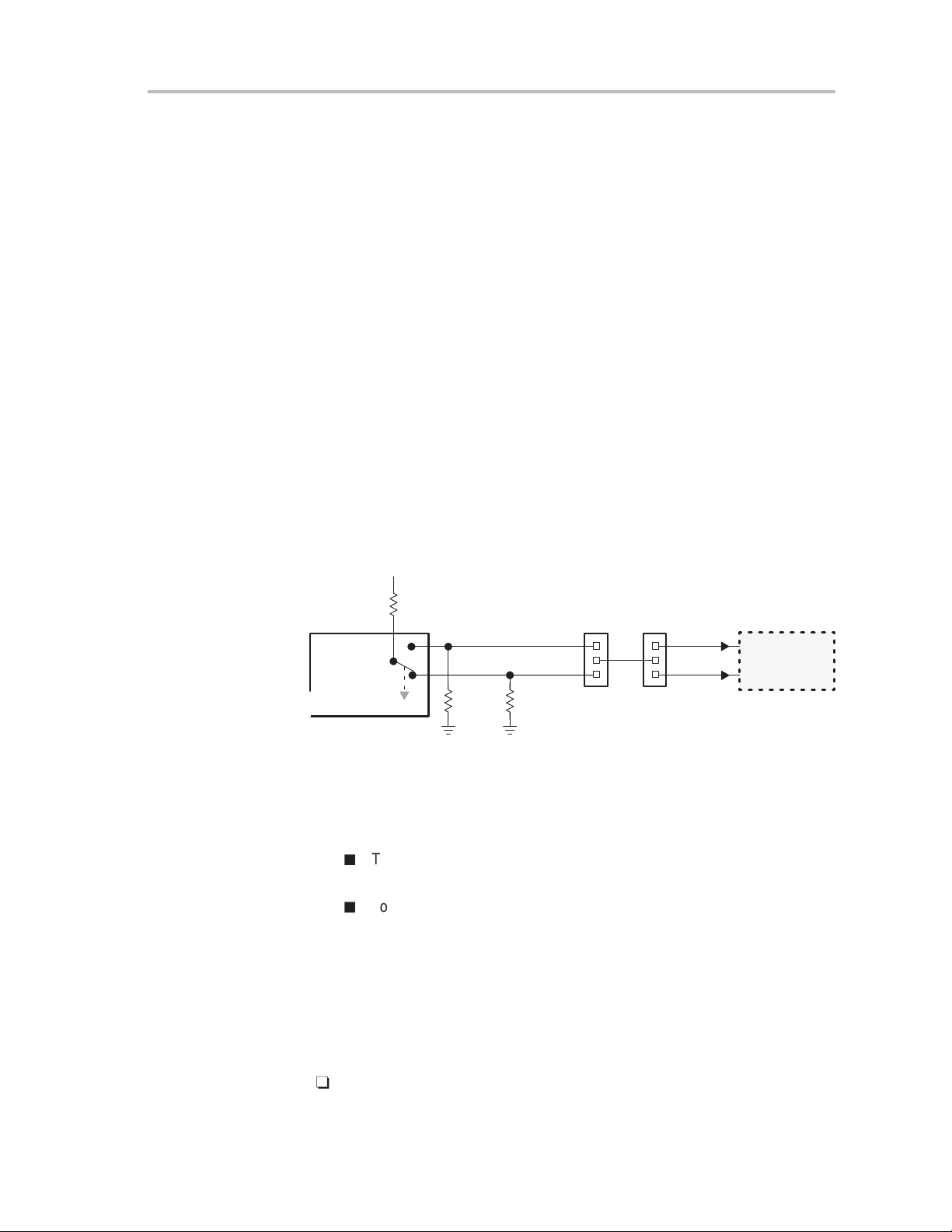
Using The TPA005D02 Class D EVM With the Plug-N-Play Platform
3.3.4 Mute
The TP A005D02 class D EVM is equipped with a mute control input pin. When
this input is tied to GND, the TP A005D02 amplifier IC on the module enters the
mute mode and dissipates very little power. When the EVM control input is tied
to V
In typical applications, as often found in notebook computers, portable audio
products, and such, the internal speakers mute when headphones are
plugged into the headphone jack, or internal speakers mute when external
speakers are connected. In applications using separate speaker and
headphone amplifiers, the one not being used can be muted to conserve
power.
3.3.4.1 Headphone Jack Control Signals
The platform headphone output jack (J10) contains an internal switch that
changes the state of a pair of control lines when a plug is inserted (Figure
3–19). Each control line is pulled down by a 1-kΩ resistor to ground (R4 and
R5). The switch in the headphone jack pulls one line or the other up to V
through a 240-Ω resistor (R3) depending on whether a plug is inserted in J10
or not.
or allowed to float, amplifier operation resumes.
DD
DD
Figure 3–19. Mute/Mode and Polarity Control
V
DD
R3
240 Ω
J10
Headphone
Jack
R4
1 kΩ
3.3.4.2 Mute/Mode Select (JP6)
A 3-pin jumper header (JP6) on the platform, functioning as an SPDT switch,
routes the control signal from the headphone jack to either the mute control
input pin or the mode control input pin of the evaluation module.
J
T o mute the TP A005D02 class D EVM using the control signal from the
platform headphone jack, jumper JP6 to
J
To isolate the TPA005D02 class D EVM from the headphone jack
switch (since the TPA005D02 class D EVM has no mode control
input), jumper JP6 to
3.3.4.3 Mute/Mode Polarity Select (JP8)
R5
1 kΩ
MODE.
Polarity
JP8 JP6
Lo
Hi
SPK
(U2–U4)
Mode
Mute
MUTE.
U2
Power
Amplifier
A second 3-pin jumper header (JP8) on the platform selects the control signal
polarity by connecting either the active-high or the active-low line from the
headphone jack to jumper JP6.
-
To mute the TPA005D02 class D EVM
headphone jack, jumper JP8 to
Lo
when
a plug is inserted into the
(the Hi position is NOT recommended).
Details
3-25
Page 40

Power Requirements
3.3.5 Power Requirements
The TP A005D02 Class D Stereo Audio Power Amplifier Evaluation Module is
designed to operate from a supply voltage between 4.5 V and 5.5 V . For best
performance (highest output power with lowest distortion), the module should
be operated on at least 5 V.
The TI Plug-N-Play Audio Amplifier Evaluation Platform with a voltage
regulator EVM installed on it can provide a regulated V
variety of unregulated V
12 V , including an onboard 9-V battery . Or, an external regulated power source
can be used to supply V
evaluation module installed on it.
Although the TP A005D02 amplifier IC draws approximately 2 A from the power
supply during continuous full power output, peak current draw can be as high
as 5 A. Any power supply connected to the platform should be capable of
providing 5 A of current to avoid clipping of the output signal during peaks.
Current consumption driving speakers at normal listening levels is typically
0.5 A or less.
The platform is equipped with overvoltage and reverse-polarity supply voltage
input protection in the form of fused crowbar circuits.
supply from a wide
DD
voltage inputs between approximately 5.5 V and
CC
voltage to the platform and the TPA005D02
DD
-
VDD voltage applied to platform screw terminals J6
MUST NOT
the absolute maximum rating for the TP A005D02 amplifier IC installed on
the evaluation module (5.5 V) or damage to the IC may result. In no case
should V
voltage of the incorrect polarity or in excess of 6.1 V be applied
DD
to screw terminals J6 of the platform, or the power protection circuit on the
line will trip.
V
DD
-
VCC voltage applied to the platform
MUST NOT
exceed the maximum
voltage input specified for the voltage regulator module installed in socket
U6 (12 V for the SLVP097), or damage to the voltage regulator module
may result. In no case should V
15 V, or the overvoltage protection circuit on the V
voltage applied to the platform exceed
CC
bus will trip.
CC
exceed
3-26
Details
Page 41
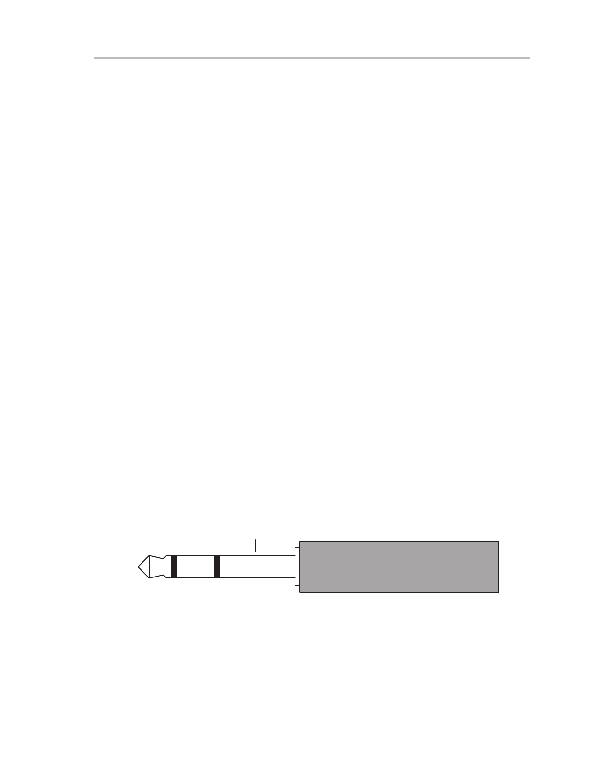
3.3.6 Inputs and Outputs
The TI Plug-N-Play Audio Amplifier Evaluation Platform is equipped with
several standard conectors for audio inputs and outputs.
3.3.6.1 Inputs
In most cases, audio signals enter the platform through either a pair of RCA
phono jacks (J3 and J5) or a miniature (1/8″) stereo phone jack (J4). Certain
signal conditioning and amplifier EVMs, however, may have additional signal
input connectors mounted on the module circuit board.
The platform audio signal input jacks (J3, J4, and J5) are of the closed-circuit
type, grounding the signal input lines when no plugs are inserted.
3.3.6.2 Outputs
Amplified audio output signals leave the platform through left and right RCA
phono jacks (J7 and J9), left and right pairs of compression connectors for
stripped speaker wires (J8), and optionally , through a miniature (1/8″ ) stereo
phone jack (J10), for headphones.
The audio output lines from the power amplifiers are separate all the way to
the edge of the platform (output jacks J7, J8, and J9)—the OUT– lines from
the power amplifier sockets are not tied to each other or to platform ground.
This allows the TPA005D02 power amplifier EVM to operate in the
highly-efficient bridge-tied load configuration when driving speakers.
Inputs and Outputs
The headphone jack (J10) is capacitively coupled to source select switch S3,
which connects J10 to the output lines of either the headphone amplifier
socket or the power amplifier sockets (Figure 3–20). Since the TPA005D02
class D EVM can drive only BTL outputs, S3 MUST ALW A YS BE SET TO THE
U5
POSITION.
Do not drive the module inputs unless speaker loads are connected to the
module outputs or the TPA005D02 amplifier IC will go into thermal shutdown.
Figure 3–20. Typical Headphone Plug
Left Right GND
Details
3-27
Page 42

Using The TPA005D02 Class D EVM Stand-Alone
3.4 Using The TPA005D02 Class D EVM Stand-Alone
Using the TPA005D02 Class D Stereo Audio Power Amplifier Evaluation
Module stand-alone is much the same as using it with the platform. The same
4.5-V to 5.5-V power supply range and the isolated OUT+ and OUT– lines for
BTL operation requirement exists.
Power can be connected to either V
pin on the module. The audio input
DD
signal should be connected to the RIN+/RIN– and LIN+/LIN– module pins for
differential signals as shown below . Single-ended input signals are applied to
RIN+ and LIN+, while RIN– and LIN– are connected to ground.
Note that the mute signal applied to the EVM mute pin must be able to supply
enough current to overcome the pullup resistor on the module (100 kΩ).
Do not drive the module inputs unless speaker loads are connected to the
module outputs or the TPA005D02 amplifier IC will go into thermal shutdown.
3.4.1 TPA005D02 Class D EVM Connected for BTL Output
Figure 3–21. TPA005D02 Class D EVM Connected for Stereo BTL Output
5 V
Audio
Input
(Right)
Audio
Input
(Left)
GND
RIN+
RIN–
Shutdown
C1
R2
R1
Q1
LIN–
LIN+
GND
Mute
T exas Instruments
R6 R7
1998
C4
C2
C3
C5
R3
R4
R5
D1
S1
SLOP223
C8
S2
C6
C7
D2
1
C10
VDD
GND
C19
C20
L1
C14
L2
C21
L3
U1
L4
GND
D3
+
C12
C13
C9
C17
C15
+
C11
VDD
TPA005D02 EVM Board Rev. A
C24
C23
C25
C26
C22
C27
Rout+
Rout–
Mute
Lout–
Lout+
Right
External Mute
Control
(active low)
Left
3-28
Details
Page 43

TP A005D02 Audio Power Amplifier Evaluation Module Parts List
3.5 TPA005D02 Audio Power Amplifier Evaluation Module Parts List
Table 3–3.TPA005D02 Class D EVM Parts List
Reference Description Size
C1, C2, C3, C6
C7, C9, C12, C13,
C16, C17, C18, C19
C4, C5, C8 Capacitor, Ceramic, 470 pF,
C20, C21 Capacitor, Ceramic, 0.047 µF,
C10, C11 Capacitor, Ceramic, 10 µF,
C14, C15 Capacitor,Tantalum, 220 µF,
C24, C25, C26, C27 Capacitor, Ceramic, 0.22 µF,
C22, C23 Capacitor, Metal Film, 1 µF,
D2, D3 LED, SM, Green, 25 mcd,
L1, L2, L3, L4 Inductor, 15 µH, 3.1 A rms,
Q1 Transistor, PNP, 60 V, 200 mA SOT-23 1 Zetex
R1, R3 Resistor, SMD, MF, 20 kΩ,
R2, R6, R7 Resistor, SMD, MF, 1 kΩ,
R4, R5 Resistor, SMD, MF, 100 kΩ, 1/16
S1, S2 Switch, Momentary, PB, 12 VDC,
U1 IC, Audio amplifier, class D,
D1 Diode, Zener, SMT, 3.9 V,
Capacitor, Ceramic, 1 µF,
16 V, Y5V, +80% –20%
50 V, X7R, 10%
50 V, X7R, 10%
16 V, Y5V, +80%–20%
10 V, 20%
25 V, X7R, 10%
50 V, ±5%, leaded
2.1 V, 120 deg
0.060 Ω
1/16 W, 5%
1/16 W, 5%
W, 5%
50 mA
5 W, 48 pin, DCA pkg
500 mW, 50 µA, 1N4686
0805 12 muRata
0603 3 muRata
0805 2 muRata
1210 2 muRata
Case E 2 AVX
0603 4 muRata
0.287 × 0.315 × 0.197 2 Panasonic
0.134 × 0.11 × 0.071 2 Lumex
0.51 × 0.37 × 0.30 4 Coilcraft
0603 2 Vishay/Dale
0603 3 Vishay/Dale
0603 2 Vishay/Dale
0.291 × 0.138 × 0.134 2 Panasonic
TSSOP48 1 TI
SOD-123 1 Motorola
EVM
Qty.
Manufacturer/
Part Number
GRM40Y5V105Z16
GRM39X7R471K50
GRM40X7R473K50
GRM235Y5V106Z16
TPSE227M010
GRM39X7R224K10
ECQ-V1H105JI
SML-LX2832GC-TR
DO3316P-153
FMMT3906CT-ND
CRCW0603203J
CRCW0603102J
CRCW0603104J
EVQ-PJS04K
TPA005D02DCA
MMSZ4686T1
Details
3-29
Page 44

TPA005D02 Class D EVM Measured Characteristics
3.6 TPA005D02 Class D EVM Measured Characteristics
The TP A005D02 Class D Stereo Audio Power Amplifier EVM was tested using
an Audio Precision 2322, a 5-V regulated DC power supply , the TI PNP Audio
Power Amplifier Evaluation Platform set up as described in Chapter 2, and 4-W
speaker loads. The results are shown in Figures 3–22 through 3–25. The
TPA005D02 class D EVM exhibits slightly less harmonic distortion at high
power levels when used in the stand-alone mode.
The EVM has a flat response over the audio frequency band, as shown in
Figure 3–22. Both channels track closely; however, the response will change
slightly with the tolerance of the filter components. The lower and upper
frequency corners can be adjusted to extend frequency response as
described in sections 3.2.3.1 and 3.2.3.2.
Figure 3–22. Frequency Response
VOLTAGE AMPLIFICATION
vs
27
26
25
24
VDD = 5 V
RL = 4Ω
FREQUENCY
Left Channel
23
22
21
20
Voltage Amplification – dB
19
18
17
16
10 20 100 1k
f – Frequency – Hz
Right Channel
10k 20k
3-30
Details
Page 45
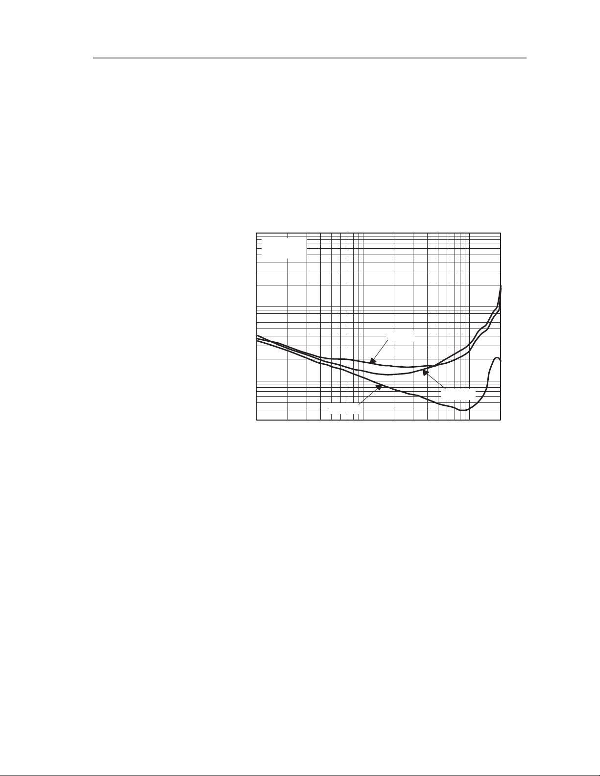
Total harmonic distortion plus noise (THD+N) versus output power is shown
in Figure 3–23. A lower power levels (less than 40 mW), most of the distortion
is contributed by the class D amplifier device. Distortion at mid and high power
levels (40 mW to 1.9 W) is a function of the output filter components,
particularly the inductors.
A slight increase in supply voltage over 5 V substantially reduces the harmonic
distortion at power levels above 500 mW.
Figure 3–23. Distortion versus Output Power
TOTAL HARMONIC DISTORTION PLUS NOISE
10
VDD = 5 V
RL = 4Ω
5
2
1
TPA005D02 Class D EVM Measured Characteristics
vs
OUTPUT POWER
0.5
0.2
0.1
0.05
THD+N – Total Harmonic Distortion Plus Noise – (%)
0.03
0.02
0.01 0.05 0.1 0.2 0.5 1
20 KHz
Po – Output Power – W
1 KHz
100 Hz
2
Details
3-31
Page 46

TPA005D02 Class D EVM Measured Characteristics
THD+N versus frequency is shown in Figure 3–24, and correlates with the data
shown in Figure 3–23. The rise in distortion at higher frequencies is due
primarily to the increase in crosstalk with frequency (Figure 3–25). The
crosstalk was measured at full output power, which is the worst-case scenario.
Crosstalk may be reduced by using shielded inductors in the output filter.
Figure 3–24. Distortion versus Frequency
TOTAL HARMONIC DISTORTION PLUS NOISE
10
VDD = 5 V
RL = 4Ω
5
2
1
vs
FREQUENCY
0.5
0.2
THD+N – Total Harmonic Distortion Plus Noise – (%)
0.1
20 100 1k
Figure 3–25. Crosstalk versus Frequency
–30
VDD = 5 V
–35
–40
–45
–50
–55
–60
–65
Crosstalk – dB
–70
–75
–80
–85
–90
RL = 4Ω
PO = 2 W
20 100 1k
1 W
1/2 W
10k 20k
CROSSTALK
vs
FREQUENCY
L to R
R to L
10k 20k
f – Frequency – Hz
3-32
Details
Page 47
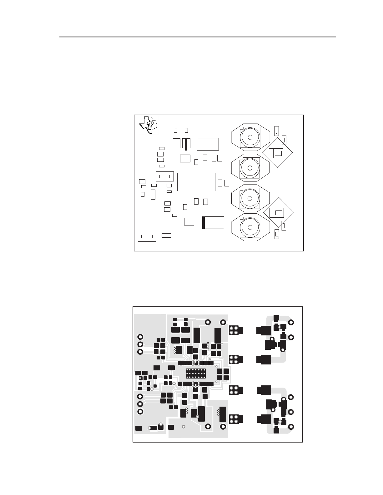
3.7 TPA005D02 Class D EVM PCB Layers
The following illustrations depict the TPA005D02 class D EVM PCB layers.
These drawings are not to scale. Gerber plots can be obtained from any TI
Sales Office.
Figure 3–26. TPA005D02 Class D EVM Silkscreen
TPA005D02 Class D EVM PCB Layers
GND
RIN+
RIN–
Shutdown
C1
R2
R1
Q1
LIN–
LIN+
GND
Mute
T exas Instruments
R6 R7
1998
C4
C2
C3
C5
R3
R4
R5
D1
S1
SLOP223
C8
S2
D2
C10
1
C6
C7
VDD
D3
C16
+
C12
C13
C9
C17
C15
+
C11
VDD
TPA005D02 EVM Board Rev. A
Figure 3–27. TPA005D02 Class D EVM Top Layer
C18
C19
GND
C20
U1
GND
C14
L1
L2
C21
L3
L4
C24
C25
C22
C23
C26
C27
Rout+
Rout–
Mute
Lout–
Lout+
Details
3-33
Page 48
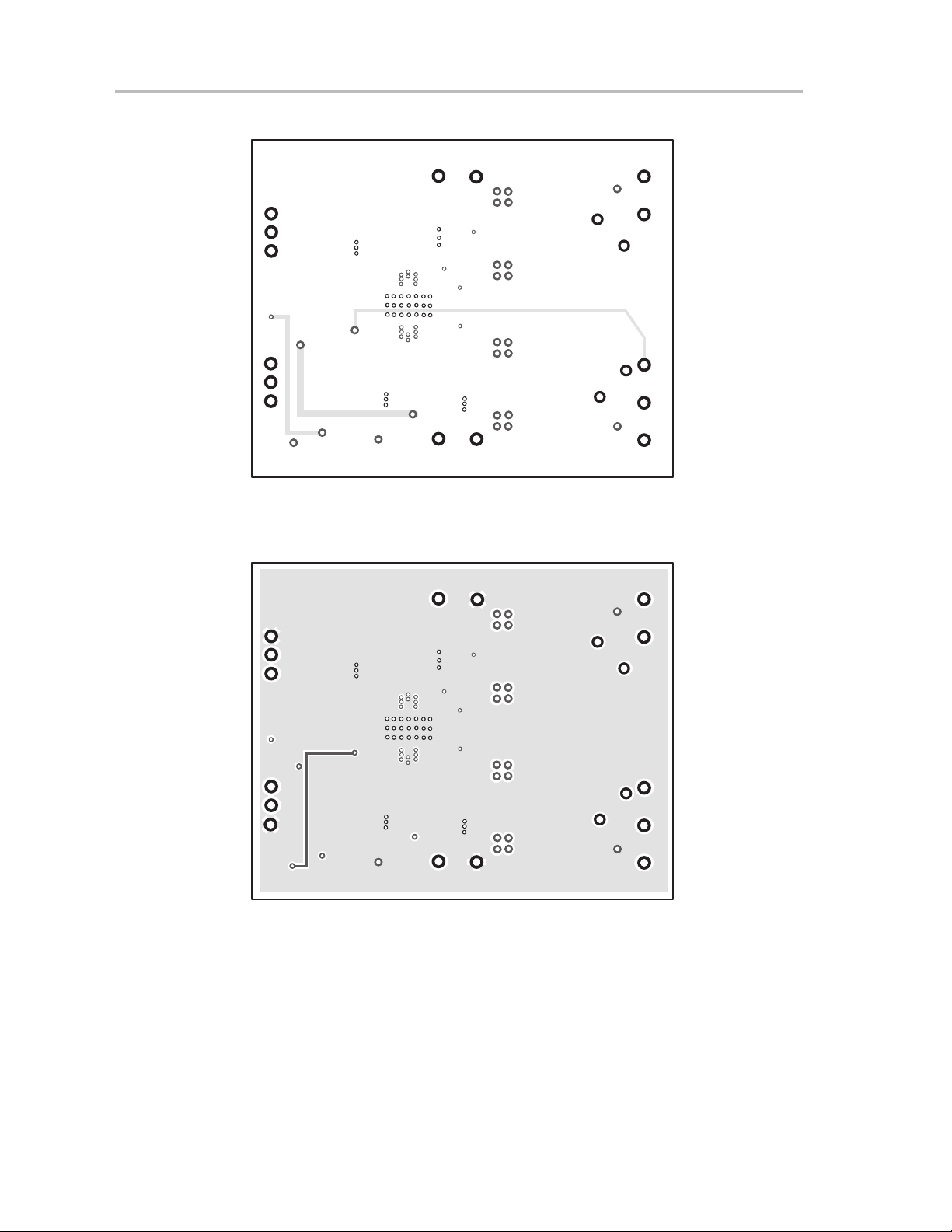
TPA005D02 Class D EVM PCB Layers
Figure 3–28. TPA005D02 Class D EVM 2nd Layer
Figure 3–29. TPA005D02 Class D EVM 3rd Layer
3-34
Details
Page 49

Figure 3–30. TPA005D02 Class D EVM Bottom Layer
TPA005D02 Class D EVM PCB Layers
Details
3-35
Page 50

3-36
Details
 Loading...