

Page 1
ThunderSWITCH II
D
Single-Chip 100-/1000-Mbit/s Device
D
Integrated Physical Coding Sublayer (PCS)
Logic Provides Direct Interface to Gigabit
Transceivers
D
Integrated Address-Lookup Engine and
Table Memory for 2-K Addresses
D
Supports IEEE Std 802.1Q Virtual-LAN
(VLAN) Tagging Scheme
D
Provides Data Path for Network
Management Information [No External
Media-Access Control (MAC) Required]
D
Full-Duplex IEEE Std 802.3 Flow Control
D
Half-Duplex Back-Pressure Flow Control
D
Fully Nonblocking Architecture Using
High-Bandwidth Rambus Memory
D
Simple Expansion Via the Gigabit Interface
for Higher-Density Port Solutions
TNETX4090
9-PORT 100-/1000-MBIT/S ETHERNET SWITCH
SPWS044E – DECEMBER 1997 – REVISED AUGUST 1999
D
Port Trunking/Load Sharing for
High-Bandwidth Interswitch Links
D
Supports Pretag Extended Port Awareness
D
EEPROM Interface for Autoconfiguration
(No CPU Required for Nonmanaged Switch)
D
Provides Direct Input/Output (DIO) Interface
for Configuration and Statistics Information
D
Supports On-Chip Per-Port Storage for
Etherstat and Remote Monitoring (RMON)
Management Information Bases (MIBs)
D
Fabricated in 2.5-/3.3-V Low-Voltage
Technology
D
Supports Ring-Cascade Mode
D
Supports Spanning Tree
D
Packaged in 352-Terminal Ball Grid Array
Package
description
The TNETX4090 is a 9-port 100-/1000-Mbit/s nonblocking Ethernet switch with an on-chip address-lookup
engine. The TNETX4090 provides a low-cost, high-performance switch solution. The TNETX4090 is a fully
manageable desktop switch solution achieved by combining the TNETX4090 with physical interfaces and
high-bandwidth rambus-based packet memory and a CPU. The TNETX4090 also provides an interface capable
of receiving and transmitting simple-network management protocol (SNMP) and bridge protocol data units
(BPDU) (spanning tree) frames.
The TNETX4090 provides eight 10-/100-Mbit/s interfaces and one 100-/1000-Mbit/s interface. In half-duplex
mode, all ports support back-pressure flow control to reduce the risk of data loss for a long burst of activity . In
the full-duplex mode of operation, the device uses IEEE Std 802.3 frame-based flow control. With full-duplex
capability , ports 0–7 support 200-Mbit/s aggregate bandwidth connections. Port 8 supports 2 Gbit/s to desktops,
high-speed servers, hubs, or other switches in the full-duplex mode. The physical coding sublayer (PCS)
function is integrated on chip to provide a direct 10-bit interface to the gigabit Ethernet transceiver. The
TNETX4090 also supports port trunking/load sharing on the 10-/100-Mbit ports. This can be used to group ports
on interswitch links to increase the effective bandwidth between the systems. In the ring-cascade mode, port 8
can be used to connect multiple devices in a ring topology , which provides a low-cost, high-port-density desktop
switch. Pretagging and extended port awareness allow the TNETX4090 to be used as a front end to a router
or crossbar switch to build a cost-effective, high-density, high-performance system.
The internal address-lookup engine (IALE) supports up to 2-K unicast/multicast and broadcast addresses and
up to 64 IEEE Std 802.1Q VLANs. For interoperability, each port can be programmed as an access port or
non-access port to recognize VLAN tags and transmit frames with VLAN tags to other systems that support
VLAN tagging. The IALE performs destination- and source-address comparisons and forwards unknown
source- and destination-address packets to ports specified via programmable masks.
Please be aware that an important notice concerning availability, standard warranty, and use in critical applications of
Texas Instruments semiconductor products and disclaimers thereto appears at the end of this data sheet.
TI, ThunderSWITCH, and ThunderSWITCH II are trademarks of Texas Instruments Incorporated.
Ethernet and Etherstat are trademarks of Xerox Corporation.
Secure Fast Switching is a trademark of Cabletron Systems, Inc.
Port-trunking and load-sharing algorithms were contributed by Cabletron Systems, Inc. and are derived from, and compatible with, Secure Fast
Switching.
PRODUCTION DATA information is current as of publication date.
Products conform to specifications per the terms of Texas Instruments
standard warranty. Production processing does not necessarily include
testing of all parameters.
POST OFFICE BOX 655303 • DALLAS, TEXAS 75265
Copyright 1998, Texas Instruments Incorporated
1
Page 2
TNETX4090
ThunderSWITCH II
9-PORT 100-/1000-MBIT/S ETHERNET SWITCH
SPWS044E – DECEMBER 1997 – REVISED AUGUST 1999
description (continued)
MII
10/100
MAC
Switching Engine
(Queue Manager)
Rambus
Controller
MII
10/100
MAC
DRAM
MII
10/100
MAC
Local Packet Switching Memory
MII
10/100
MAC
VLAN 802.1Q
Address-Lookup Engine
2048 CAM
10/100
MAC
and
MII
MII
10/100
MAC
10/100
MAC
100/1000
MAC
GMII/PMA
MII
MII
10/100
MAC
Hardware
RMON
and
Etherstat
MIB
EEPROM
I/F
CPU I/F
With
DMA
100-M
Management
MAC
MDIO
I/F
LED
I/F
JTAG
I/F
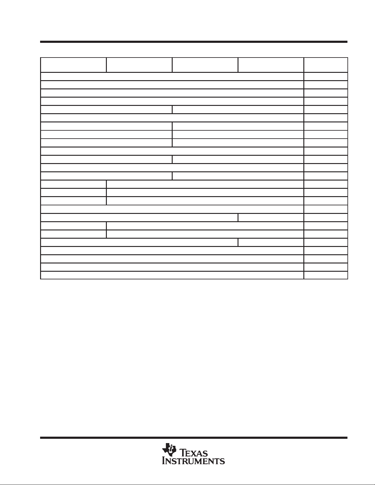
Figure 1. TNETX4090 Block Diagram
Statistics for the Etherstat, SNMP, and remote-monitoring management information base (RMON MIB) are
independently collected for each of the nine ports. Access to the statistics counters is provided via the direct
input/output (DIO) interface. Management frames can be received and transmitted via the DIO interface,
creating a complete network management solution. Figure 1 is a block diagram of the TNETX4090.
The TNETX4090 memory solution combines low cost and extremely high bandwidth, using 600-Mbit/pin/s
concurrent RDRAM. The packet memory has been implemented to maximize efficiency with the RDRAM
architecture. Data is buffered internally and transferred to/from packet memory in 128-byte bursts. Extremely
high-memory bandwidth is maintained, allowing all ports to be active without bottlenecking at the memory buffer .
The TNETX4090 is fabricated with a 2.5-V technology . The inputs are 3.3-V tolerant and the outputs are capable
of directly interfacing to TTL levels. This provides the customer with a broad choice of interfacing device options.
Signal names and their terminal assignments are sorted alphabetically in Table 1.
2
POST OFFICE BOX 655303 • DALLAS, TEXAS 75265
Page 3

ThunderSWITCH II
Description 1. . . . . . . . . . . . . . . . . . . . . . . . . . . . . . . . . . . . . . . . . . .
Terminal Functions 7. . . . . . . . . . . . . . . . . . . . . . . . . . . . . . . . . . . .
DIO Interface Description 18. . . . . . . . . . . . . . . . . . . . . . . . . . . . .
Receiving/Transmitting Management Frames 27. . . . . . . . . . .
State of DIO Signal Terminals During Hardware Reset 28. . .
IEEE Std 802.1Q VLAN Tags on the NM Port 28. . . . . . . . . . .
Frame Format on the NM Port 28. . . . . . . . . . . . . . . . . . . . . . . .
Full-Duplex NM Port 31. . . . . . . . . . . . . . . . . . . . . . . . . . . . . . . .
NM Bandwidth and Priority 31. . . . . . . . . . . . . . . . . . . . . . . . . . .
Interrupt Processing 31. . . . . . . . . . . . . . . . . . . . . . . . . . . . . . . .
PHY Management Interface 31. . . . . . . . . . . . . . . . . . . . . . . . . . .
MAC Interface 32. . . . . . . . . . . . . . . . . . . . . . . . . . . . . . . . . . . . . . . .
Receive Control 32. . . . . . . . . . . . . . . . . . . . . . . . . . . . . . . . . . . .
Giant (Long) Frames 32. . . . . . . . . . . . . . . . . . . . . . . . . . . . . . . .
Short Frames 32. . . . . . . . . . . . . . . . . . . . . . . . . . . . . . . . . . . . . .
Receive Filtering of Frames 32. . . . . . . . . . . . . . . . . . . . . . . . . .
Data Transmission 32. . . . . . . . . . . . . . . . . . . . . . . . . . . . . . . . . .
Transmit Control 32. . . . . . . . . . . . . . . . . . . . . . . . . . . . . . . . . . .
Adaptive Performance Optimization (APO) 33. . . . . . . . . . . . .
Interframe Gap Enforcement 33. . . . . . . . . . . . . . . . . . . . . . . . .
Backoff 33. . . . . . . . . . . . . . . . . . . . . . . . . . . . . . . . . . . . . . . . . . .
Receive Versus Transmit Priority 33. . . . . . . . . . . . . . . . . . . . .
10-/100-Mbit/s MII (ports 0–7) 34. . . . . . . . . . . . . . . . . . . . . . . .
Speed, Duplex, and Flow-Control Negotiation 34. . . . . . . . . .
100-/1000-Mbit/s PHY Interface (Port 8) 36. . . . . . . . . . . . . . . . .
Speed, Duplex, and Flow-Control Negotiation 36. . . . . . . . . .
Full-Duplex Hardware Flow Control 37. . . . . . . . . . . . . . . . . . .
Pretagging and Extended Port Awareness 38. . . . . . . . . . . . .
Ring-Cascade Topology 40. . . . . . . . . . . . . . . . . . . . . . . . . . . . .
EEPROM Interface 42. . . . . . . . . . . . . . . . . . . . . . . . . . . . . . . . . . . .
Interaction of EEPROM Load With the SIO Register 43. . . . .
Summary of EEPROM Load Outcomes 43. . . . . . . . . . . . . . . .
Compatibility With Future Device Revisions 44. . . . . . . . . . . .
LED Interface 44. . . . . . . . . . . . . . . . . . . . . . . . . . . . . . . . . . . . . . . .
Lamp Test 45. . . . . . . . . . . . . . . . . . . . . . . . . . . . . . . . . . . . . . . . .
Multi-LED Display 45. . . . . . . . . . . . . . . . . . . . . . . . . . . . . . . . . .
TNETX4090
9-PORT 100-/1000-MBIT/S ETHERNET SWITCH
SPWS044E – DECEMBER 1997 – REVISED AUGUST 1999
Contents
PCS Duplex LED 45. . . . . . . . . . . . . . . . . . . . . . . . . . . . . . . . . . . . . . . .
RDRAM Interface 45. . . . . . . . . . . . . . . . . . . . . . . . . . . . . . . . . . . . . . . .
JTAG Interface 47. . . . . . . . . . . . . . . . . . . . . . . . . . . . . . . . . . . . . . . . . .
HIGHZ Instruction 47. . . . . . . . . . . . . . . . . . . . . . . . . . . . . . . . . . . . .
RACBIST Instruction 47. . . . . . . . . . . . . . . . . . . . . . . . . . . . . . . . . . .
Frame Routing 48. . . . . . . . . . . . . . . . . . . . . . . . . . . . . . . . . . . . . . . . . .
VLAN Support 48. . . . . . . . . . . . . . . . . . . . . . . . . . . . . . . . . . . . . . . .
Address Maintenance 49. . . . . . . . . . . . . . . . . . . . . . . . . . . . . . . . . .
Port Trunking/Load Sharing 54. . . . . . . . . . . . . . . . . . . . . . . . . . . . . .
Port-Trunking Example 55. . . . . . . . . . . . . . . . . . . . . . . . . . . . . . . . .
Extended Port Awareness 55. . . . . . . . . . . . . . . . . . . . . . . . . . . . . .
Flow Control 56. . . . . . . . . . . . . . . . . . . . . . . . . . . . . . . . . . . . . . . . . . . .
Other Flow-Control Mechanisms 57. . . . . . . . . . . . . . . . . . . . . . . . .
System Test Capabilities 57. . . . . . . . . . . . . . . . . . . . . . . . . . . . . . .
RDRAM 57. . . . . . . . . . . . . . . . . . . . . . . . . . . . . . . . . . . . . . . . . . . . . .
Writing RDRAM 57. . . . . . . . . . . . . . . . . . . . . . . . . . . . . . . . . . . . . . .
Reading RDRAM 58. . . . . . . . . . . . . . . . . . . . . . . . . . . . . . . . . . . . . .
Internal Wrap Test 58. . . . . . . . . . . . . . . . . . . . . . . . . . . . . . . . . . . . .
Duplex Wrap Test 59. . . . . . . . . . . . . . . . . . . . . . . . . . . . . . . . . . . . .
Absolute Maximum Ratings 60. . . . . . . . . . . . . . . . . . . . . . . . . . . . . .
Recommended Operating Conditions 60. . . . . . . . . . . . . . . . . . . . .
Electrical Characteristics 61. . . . . . . . . . . . . . . . . . . . . . . . . . . . . . . .
Timing Requirements 61. . . . . . . . . . . . . . . . . . . . . . . . . . . . . . . . . . . .
JTAG Interface 61. . . . . . . . . . . . . . . . . . . . . . . . . . . . . . . . . . . . . . . .
Control Signals 61. . . . . . . . . . . . . . . . . . . . . . . . . . . . . . . . . . . . . . . .
Physical Medium Attachment Interface (Port 8) 62. . . . . . . . . . . .
Receive 62. . . . . . . . . . . . . . . . . . . . . . . . . . . . . . . . . . . . . . . . . . . . . .
Transmit 63. . . . . . . . . . . . . . . . . . . . . . . . . . . . . . . . . . . . . . . . . . . . .
GMII (Port 8) 64. . . . . . . . . . . . . . . . . . . . . . . . . . . . . . . . . . . . . . . . . .
MII (Ports 0–8) 66. . . . . . . . . . . . . . . . . . . . . . . . . . . . . . . . . . . . . . . .
RDRAM Interface 68. . . . . . . . . . . . . . . . . . . . . . . . . . . . . . . . . . . . .
DIO Interface 69. . . . . . . . . . . . . . . . . . . . . . . . . . . . . . . . . . . . . . . . .
EEPROM Interface 71. . . . . . . . . . . . . . . . . . . . . . . . . . . . . . . . . . . .
LED Interface 72. . . . . . . . . . . . . . . . . . . . . . . . . . . . . . . . . . . . . . . . .
Parameter Measurement Information 73. . . . . . . . . . . . . . . . . . . . . .
Mechanical Data 76. . . . . . . . . . . . . . . . . . . . . . . . . . . . . . . . . . . . . . . .
POST OFFICE BOX 655303 • DALLAS, TEXAS 75265
3
Page 4
TNETX4090
ThunderSWITCH II
9-PORT 100-/1000-MBIT/S ETHERNET SWITCH
SPWS044E – DECEMBER 1997 – REVISED AUGUST 1999
26 24 22 20 18 16 14 12 10 8 6 4 225 23 21 19 17 15 13 11 9 7 5 3 1
GGP PACKAGE
(BOTTOM VIEW)
A
B
C
D
E
F
G
H
J
K
L
M
N
P
R
T
U
V
W
Y
AA
AB
AC
AD
AE
AF
4
POST OFFICE BOX 655303 • DALLAS, TEXAS 75265
Page 5
ThunderSWITCH II
9-PORT 100-/1000-MBIT/S ETHERNET SWITCH
TNETX4090
SPWS044E – DECEMBER 1997 – REVISED AUGUST 1999
Table 1. Signal-to-Ball Mapping (Signal Names Sorted Alphabetically)
SIGNAL
NAME
DBUS_CTL
DBUS_DATA0
DBUS_DATA1
DBUS_DATA2
DBUS_DATA3
DBUS_DATA4
DBUS_DATA5
DBUS_DATA6
DBUS_DATA7
DBUS_DATA8
DBUS_EN
DCCTRL
DRX_CLK
DTX_CLK
DVREF
ECLK
EDIO
FLOW
GND
GND
GND
GND
GND
GND
GND
GND
GND
GND
GND
GND
GND
GND
GND
GND
GND
GND
GND
GND
GND
GND
GND
GND
GND
GND
GND
GND
GND
GND
GND
GND
GND
GND
GND
GND
GND
GND
GND
GND
GND
GND
BALL
NO.
Y26
AC26
AA24
AB26
Y24
V24
U25
U26
T26
R25
T25
P24
V26
V25
AA26
L26
M26
AF8
A1
A2
A13
A14
A25
A26
AF13
AF14
B1
B3
B24
B26
C2
C25
N1
N26
P1
P25
P26
R23
R24
R26
T24
U23
W23
W24
W25
W26
Y23
Y25
AA23
AA25
AB25
AD2
AD25
AE1
AE3
AE24
AE26
AF1
AF2
AF25
SIGNAL
NAME
GND
GNDa
L08_DPLX
LED_CLK
LED_DATA
M00-COL
M00_CRS
M00_LINK
M00_RCLK
M00_RENEG
M00_RXD0
M00_RXD1
M00_RXD2
M00_RXD3
M00_RXDV
M00_RXER
M00_TCLK
M00_TXD0
M00_TXD1
M00_TXD2
M00_TXD3
M00_TXEN
M00_TXER
M01_COL
M01_CRS
M01_LINK
M01_RCLK
M01_RENEG
M01_RXD0
M01_RXD1
M01_RXD2
M01_RXD3
M01_RXDV
M01_RXER
M01_TCLK
M01_TXD0
M01_TXD1
M01_TXD2
M01_TXD3
M01_TXEN
M01_TXER
M02_COL
M02_CRS
M02_LINK
M02_RCLK
M02_RENEG
M02_RXD0
M02_RXD1
M02_RXD2
M02_RXD3
M02_RXDV
M02_RXER
M02_TCLK
M02_TXD0
M02_TXD1
M02_TXD2
M02_TXD3
M02_TXEN
M02_TXER
M03_COL
BALL
NO.
AF26
U24
AE18
AD19
AE19
C21
B21
B19
A21
C26
A20
B20
C20
D20
D19
C19
B23
A23
A22
B22
C22
D22
D21
D16
C16
B14
B16
D26
A15
B15
C15
D15
A16
C14
C17
A19
A18
B18
C18
B17
A17
C11
B11
A9
A11
D1
A10
B10
C10
D10
C9
B9
C13
A12
B12
C12
D12
B13
D11
A6
SIGNAL
NAME
M03_CRS
M03_LINK
M03_RCLK
M03_RENEG
M03_RXD0
M03_RXD1
M03_RXD2
M03_RXD3
M03_RXDV
M03_RXER
M03_TCLK
M03_TXD0
M03_TXD1
M03_TXD2
M03_TXD3
M03_TXEN
M03_TXER
M04_COL
M04_CRS
M04_LINK
M04_RCLK
M04_RENEG
M04_RXD0
M04_RXD1
M04_RXD2
M04_RXD3
M04_RXDV
M04_RXER
M04_TCLK
M04_TXD0
M04_TXD1
M04_TXD2
M04_TXD3
M04_TXEN
M04_TXER
M05_COL
M05_CRS
M05_LINK
M05_RCLK
M05_RENEG
M05_RXD0
M05_RXD1
M05_RXD2
M05_RXD3
M05_RXDV
M05_RXER
M05_TCLK
M05_TXD0
M05_TXD1
M05_TXD2
M05_TXD3
M05_TXEN
M05_TXER
M06_COL
M06_CRS
M06_LINK
M06_RCLK
M06_RENEG
M06_RXD0
M06_RXD1
BALL
NO.
B6
A4
C6
C1
A5
B5
C5
D5
C4
B4
A8
A7
B7
C7
D7
B8
C8
H2
H1
L3
J3
F3
J1
K1
K2
K3
J2
L4
F1
G1
G2
G3
G4
H4
H3
N2
P3
T2
P2
F2
R1
R2
R3
R4
T4
T3
L2
M1
M2
M3
M4
L1
N3
V1
W3
AA1
W2
AA3
Y1
Y2
SIGNAL
NAME
M06_RXD2
M06_RXD3
M06_RXDV
M06_RXER
M06_TCLK
M06_TXD0
M06_TXD1
M06_TXD2
M06_TXD3
M06_TXEN
M06_TXER
M07_COL
M07_CRS
M07_LINK
M07_RCLK
M07_RENEG
M07_RXD0
M07_RXD1
M07_RXD2
M07_RXD3
M07_RXDV
M07_RXER
M07_TCLK
M07_TXD0
M07_TXD1
M07_TXD2
M07_TXD3
M07_TXEN
M07_TXER
M08_COL
M08_CRS
M08_EWRAP
M08_GTCLK
M08_LINK
M08_LREF
M08_MII
M08_PMA
M08_RCLK
M08_RFCLK
M08_RXD0
M08_RXD1
M08_RXD2
M08_RXD3
M08_RXD4
M08_RXD5
M08_RXD6
M08_RXD7
M08_RXDV
M08_RXER
M08_TXD0
M08_TXD1
M08_TXD2
M08_TXD3
M08_TXD4
M08_TXD5
M08_TXD6
M08_TXD7
M08_TXEN
M08_TXER
MDCLK
BALL
NO.
Y3
Y4
W1
AA2
T1
U1
U2
U3
U4
V3
V2
AC6
AD6
AF3
AE6
AD1
AF7
AE7
AD7
AC7
AC8
AD8
AD4
AF5
AE5
AD5
AC5
AE4
AF4
AD12
AC12
AE13
AF17
AE17
AF12
AC17
AD17
AE12
AD13
AF9
AE9
AD9
AF10
AE10
AD10
AF11
AE11
AD11
AC11
AF16
AE16
AD16
AC16
AF15
AE15
AD15
AC15
AE14
AD14
K26
SIGNAL
NAME
MDIO
MRESET
NC
NC
NC
NC
NC
NC
NC
NC
NC
NC
NC
NC
NC
NC
NC
NC
NC
NC
NC
NC
NC
NC
NC
NC
NC
NC
NC
NC
NC
NC
NC
NC
NC
NC
NC
NC
NC
NC
NC
NC
NC
NC
NC
NC
NC
NC
NC
NC
NC
NC
NC
NC
BALL
NO.
K25
K24
A3
A24
C23
D2
D3
D6
D24
D25
E1
E2
E3
E4
E23
E24
E25
E26
F4
F23
F24
F25
F26
G23
G24
G25
G26
H24
H25
H26
J24
J25
J26
K23
N23
N24
N25
AA4
AB1
AB2
AB3
AB4
AB23
AB24
AC1
AC2
AC3
AC24
AC25
AD18
AD26
AE8
AF6
AF18
POST OFFICE BOX 655303 • DALLAS, TEXAS 75265
5
Page 6
TNETX4090
ThunderSWITCH II
9-PORT 100-/1000-MBIT/S ETHERNET SWITCH
SPWS044E – DECEMBER 1997 – REVISED AUGUST 1999
Table 2. Signal-to-Ball Mapping (Signal Names Sorted Alphabetically) (Continued)
SIGNAL
NAME
RESET
SAD0
SAD1
SCS
SDATA0
SDATA1
SDATA2
SDATA3
SDATA4
SDATA5
SDATA6
SDATA7
BALL
NO.
M23
AF22
AE22
AD22
AF20
AE20
AD20
AC20
AF21
AE21
AD21
AC21
SIGNAL
NAME
SDMA
SINT
SRDY
SRNW
SRXRDY
STXRDY
TCLK
TDI
TDO
TMS
TRST
V
DD(2.5)
BALL
NO.
AF24
AF19
AF23
AC22
AE23
AD23
L24
M24
L23
M25
L25
B2
SIGNAL
V
DD(2.5)
V
DD(2.5)
V
DD(2.5)
V
DD(2.5)
V
DD(2.5)
V
DD(2.5)
V
DD(2.5)
V
DD(2.5)
V
DD(2.5)
V
DD(2.5)
V
DD(2.5)
V
DD(2.5)
NAME
BALL
NO.
B25
C3
C24
D4
D9
D14
D18
D23
J4
J23
N4
P23
SIGNAL
V
DD(2.5)
V
DD(2.5)
V
DD(2.5)
V
DD(2.5)
V
DD(2.5)
V
DD(2.5)
V
DD(2.5)
V
DD(2.5)
V
DD(2.5)
V
DD(2.5)
V
DD(2.5)
V
DD(3.3)
NAME
BALL
NO.
V4
V23
AC4
AC9
AC13
AC18
AC23
AD3
AD24
AE2
AE25
D8
SIGNAL
V
DD(3.3)
V
DD(3.3)
V
DD(3.3)
V
DD(3.3)
V
DD(3.3)
V
DD(3.3)
V
DD(3.3)
V
DD(3.3)
V
DD(3.3)
VDDa
NAME
(2.5)
BALL
NO.
D13
D17
H23
K4
P4
W4
AC10
AC14
AC19
T23
6
POST OFFICE BOX 655303 • DALLAS, TEXAS 75265
Page 7
I/O
DESCRIPTION
I/O
DESCRIPTION
ThunderSWITCH II
9-PORT 100-/1000-MBIT/S ETHERNET SWITCH
SPWS044E – DECEMBER 1997 – REVISED AUGUST 1999
TNETX4090
Terminal Functions
JTAG interface
TERMINAL
NAME NO.
TCLK L24
TDI M24
TDO L23
TMS M25
TRST L25
†
Internal resistors are provided to pull signals to known values. The system designers should determine if additional pullups or pulldowns are
required in their systems.
INTERNAL
RESISTOR
I Pullup
I Pullup
O None
I Pullup
I Pullup
†
T est clock. Clocks state information and test data into and out of the TNETX4090 during operation
of the test port.
T est data input. Serially shifts test data and test instructions into the TNETX4090 during operation
of the test port. An internal pullup resistor is provided on TDI to ensure JTAG compliance.
T est data out. Serially shifts test data and test instructions out of the TNETX4090 during operation
of the test port.
T est mode select. Controls the state of the test-port controller. An internal pullup resistor is provided
on TMS to ensure JTAG compliance.
T est reset. Asynchronously resets the test-port controller . An internal pullup resistor is provided on
TRST
to ensure JTAG compliance.
control logic interface
TERMINAL
NAME NO.
RESET
FLOW
M23 I
AF8 O
Device reset. Asserted for a minimum of 100 µs after power supplies and clocks have stabilized. The system clock
must be operational during reset.
Flow control. When flow control is activated (flow in SysControl = 1) and the number of free external memory
buffers is below the threshold indicated in FlowThreshold, FLOW is asserted.
100-/1000-Mbit/s MAC interface [gigabit media-independent interface (GMII) (port 8)]
TERMINAL
NAME
M08_PMA
M08_MII
†
Internal resistors are provided to pull signals to known values. The system designers should determine if additional pullups or pulldowns are
required in their systems.
INTERNAL
I/O
RESISTOR
I Pullup
I Pullup
†
PMA mode. PMA mode can be selected by either pulling M08_PMA low externally, or by setting the
reqpma bit in the PortxControl register. If M08_PMA
either an MII or GMII interface, as determined by the value of the M08_MII
MII or GMII selection. The value of this terminal is ignored if M08_PMA = 0. 100-Mbit/s MII mode can
be selected by either pulling M08_MII
register. If M08_MII
is allowed to float high, the port is configured as a GMII interface.
DESCRIPTION
is allowed to float high, the port is configured as
terminal.
low externally, or by setting the req100 bit in the PortxControl
POST OFFICE BOX 655303 • DALLAS, TEXAS 75265
7
Page 8
TNETX4090
ThunderSWITCH II
9-PORT 100-/1000-MBIT/S ETHERNET SWITCH
SPWS044E – DECEMBER 1997 – REVISED AUGUST 1999
Terminal Functions (Continued)
100-/1000-Mbit/s MAC interface (GMII mode)
TERMINAL
NAME
M08_COL
M08_CRS
M08_EWRAP
M08_GTCLK
M08_LINK
M08_LREF O None
M08_RCLK
M08_RFCLK
M08_RXD7
M08_RXD6
M08_RXD5
M08_RXD4
M08_RXD3
M08_RXD2
M08_RXD1
M08_RXD0
M08_RXDV
M08_RXER
M08_TXD7
M08_TXD6
M08_TXD5
M08_TXD4
M08_TXD3
M08_TXD2
M08_TXD1
M08_TXD0
M08_TXEN
M08_TXER
†
Internal resistors are provided to pull signals to known values. The system designers should determine if additional pullups or pulldowns are
required in their systems.
INTERNAL
I/O
RESISTOR
I Pulldown
I Pulldown Carrier sense. M08_CRS indicates a frame carrier signal is being received.
O None Enable wrap. M08_EWRAP reflects the state of the loopback bit in the PCS8Control register.
O None Transmit clock. Transmit clock output to attached physical layer (PHY) device.
I Pulldown
I Pullup Receive clock. Receive clock source from the attached PHY.
I Pullup
I Pullup
I Pulldown
I Pulldown Receive error. M08_RXER indicates reception of a coding error on received data.
O None
O None
O None
†
Collision sense. Assertion of M08_COL during half-duplex operation indicates network collision.
Additionally, during full-duplex operation, transmission of new frames does not commence if this
terminal is asserted.
Connection status. M08_LINK indicates the presence of port connection.
– If M08_LINK = 0, there is no link.
– If M08_LINK = 1, the link is OK.
Renegotiate. M08_LREF indicates to the attached PHY device that this device wishes to negotiate
a new configuration.
– Following a 0-to-1 transition of neg in PortxControl, M08_LREF is asserted low, and
remains low until M08_LINK goes low. If M08_LINK was already low, M08_LREF
activated for at least one cycle.
– M08_LREF
of M08_LINK.
Reference clock. Reference clock, used as the clock source for the transmit side of this port and
to generate M08_GTCLK.
Receive data. Byte receive data from the attached PHY. When M08_RXDV is asserted, these
signals carry receive data. Data on these signals is synchronous to M08_RCLK.
Receive data valid. M08_RXDV indicates data on M08_RXD7–M08_RXD0 is valid. This signal is
synchronous to M08_RCLK.
Transmit data. Byte transmit data. When M08_TXEN is asserted, these signals carry transmit data.
Data on these signals is synchronous to M08_GTCLK.
Transmit enable. M08_TXEN indicates valid transmit data on M08_TXD7–M08_TXD0. This signal
is synchronous to M08_GTCLK.
Transmit error. M08_TXER allows coding errors to be propagated between the media-access
control (MAC) and the attached PHY . It is asserted at the end of an under-running frame, enabling
the device to force a coding error.
is asserted low for as long as initd in SysControl = 0, regardless of the state
DESCRIPTION
is still
8
POST OFFICE BOX 655303 • DALLAS, TEXAS 75265
Page 9

ThunderSWITCH II
Terminal Functions (Continued)
100-/1000-Mbit/s MAC interface [physical media attachment (PMA) mode]
TERMINAL
NAME
M08_COL
M08_CRS
M08_EWRAP
M08_GTCLK
M08_LINK
M08_LREF O None
M08_RCLK
M08_RFCLK
M08_RXD7
M08_RXD6
M08_RXD5
M08_RXD4
M08_RXD3
M08_RXD2
M08_RXD1
M08_RXD0
M08_RXDV
M08_RXER
M08_TXD7
M08_TXD6
M08_TXD5
M08_TXD4
M08_TXD3
M08_TXD2
M08_TXD1
M08_TXD0
M08_TXEN
M08_TXER
INTERNAL
I/O
RESISTOR
I Pulldown
I Pulldown Unused. This terminal can be left unconnected.
O None
O None Transmit clock. Transmit clock output to attached SERDES device.
I Pulldown
I Pullup
I Pullup
I Pullup
I Pulldown
I Pulldown
O None
O None
O None
Receive byte clock 1. M08_COL is used to input receive byte clock 1 from the attached SERDES
device.
Enable wrap. Output to attached SERDES device used to enable loopback testing of that device.
M08_EWRAP is asserted when loopback in PCSxControl = 1.
Signal detect. This can be connected to the signal detect output from the external SERDES device.
– If M08_LINK = 0, there is no signal.
– If M08_LINK = 1, signal is present.
Lock to reference. M08_LREF is asserted low during hard reset or when lckref in PortxControl = 1.
It is used by the external SERDES device to lock to its reference clock.
Receive byte clock 0. M08_RCLK is used to input receive byte clock 0 from the attached SERDES
device.
Reference clock. Reference clock, used as the clock source for the transmit side of this port and
to generate M08_GTCLK. M08_RFCLK provides the clock source for the entire internal PCS
sublayer.
Receive data. Least significant eight bits of the 10-bit receive code group. Even-numbered code
groups are latched with M08_COL, and odd-numbered code groups are latched with M08_RCLK.
Receive data valid. M08_RXDV is used to receive the 9th bit of the 10-bit PMA code groups.
Even-numbered code groups are latched with M08_COL, and odd-numbered code groups are
latched with M08_RCLK.
Receive error. M08_RXER is used to receive the 10th bit of the 10-bit PMA code groups.
Even-numbered code groups are latched with M08_COL, and odd-numbered code groups are
latched with M08_RCLK.
Transmit data. Least significant eight bits of the 10-bit transmit code group. Data on these signals
is synchronous to M08_GTCLK.
Transmit enable. M08_TXEN is used to transmit the 9th bit of the 10-bit PMA code groups. Data
on this signal is synchronous to M08_GTCLK.
Transmit error . M08_TXER is used to transmit the 10th bit of the 10-bit PMA code groups. Data on
this signal is synchronous to M08_GTCLK.
9-PORT 100-/1000-MBIT/S ETHERNET SWITCH
SPWS044E – DECEMBER 1997 – REVISED AUGUST 1999
DESCRIPTION
TNETX4090
POST OFFICE BOX 655303 • DALLAS, TEXAS 75265
9
Page 10
TNETX4090
ThunderSWITCH II
9-PORT 100-/1000-MBIT/S ETHERNET SWITCH
SPWS044E – DECEMBER 1997 – REVISED AUGUST 1999
Terminal Functions (Continued)
100-/1000-Mbit/s MAC interface [media-independent interface (MII) mode]
TERMINAL
NAME
M08_COL
M08_CRS
M08_EWRAP
M08_GTCLK
M08_LINK
M08_LREF O None
M08_RCLK
M08_RFCLK
M08_RXD7
M08_RXD6
M08_RXD5 I/O
M08_RXD4 I/O
M08_RXD3
M08_RXD2
M08_RXD1
M08_RXD0
M08_RXDV
M08_RXER
M08_TXD7
M08_TXD6
M08_TXD5
M08_TXD4
M08_TXD3
M08_TXD2
M08_TXD1
M08_TXD0
†
Not a true bidirectional terminal. It can only be actively pulled down.
INTERNAL
I/O
RESISTOR
Collision sense. Assertion of M08_COL during half-duplex operation indicates network collision.
I Pulldown
I Pulldown Carrier sense. M08_CRS indicates a frame carrier signal is being received.
O None Enable wrap. M08_EWRAP reflects the state of the loopback bit in the PCS8Control register.
O None Unused. This terminal can be left unconnected.
I Pulldown
I Pullup Receive clock. Receive clock source from the attached PHY or PMI device.
I Pullup Transmit clock. Transmit clock from the attached PHY or PMI device.
I Pullup Unused. These terminals can be left unconnected.
†
Pullup
†
Pullup
I Pullup
I Pulldown
I Pulldown Receive error. Indicates reception of a coding error on received data.
O None Unused. These terminals can be left unconnected, but are driven low.
O None
Additionally, during full-duplex operation, transmission of new frames does not commence if this
terminal is asserted.
Connection status. M08_LINK indicates the presence of port connection.
– If M08_LINK = 0, there is no link.
– If M08_LINK = 1, the link is OK.
Renegotiate. M08_LREF indicates to the attached PHY device that this device wishes to negotiate
a new configuration.
– Following a 0-to-1 transition of neg in PortxControl, M08_LREF is asserted low, and
remains low until M08_LINK goes low. If M08_LINK was already low, M08_LREF
activated for at least one cycle.
– M08_LREF
of M08_LINK.
IEEE Std 802.3x pause frame support selection
– If pulled low either internally or by the attached PHY or PMI device, M08_RXD5 causes the
port to not support pause frames.
– If not pulled low, the port does not support pause frames.
Duplex selection [force half duplex (active low)]
– If pulled low either internally or by the attached PHY or PMI device, the port operates in
half-duplex mode.
– If not pulled low, the port operates in full-duplex mode.
Receive data. Nibble-wide receive data from the attached PHY or PMI device. When M08_RXDV
is asserted, these signals carry receive data. Data on these signals is synchronous to M08_RCLK.
Receive data valid. M08_RXDV indicates data on M08_RXD3–M08_RXD0 is valid. This signal is
synchronous to M08_RCLK.
Transmit data. Nibble-wide transmit data. When M08_TXEN is asserted, these signals carry
transmit data. Data on these signals is synchronous to M08_RFCLK.
is asserted low for as long as initd in SysControl = 0, regardless of the state
DESCRIPTION
is still
10
POST OFFICE BOX 655303 • DALLAS, TEXAS 75265
Page 11

I/O
DESCRIPTION
ThunderSWITCH II
Terminal Functions (Continued)
100-/1000-Mbit/s MAC interface [media-independent interface (MII) mode] (continued)
TERMINAL
NAME
M08_TXEN
M08_TXER
10-/100-Mbit/s MAC interface (MII mode) (ports 0–7)
TERMINAL
NAME NO.
M00_COL
M01_COL
M02_COL
M03_COL
M04_COL
M05_COL
M06_COL
M07_COL
M00_CRS
M01_CRS
M02_CRS
M03_CRS
M04_CRS
M05_CRS
M06_CRS
M07_CRS
M00_LINK
M01_LINK
M02_LINK
M03_LINK
M04_LINK
M05_LINK
M06_LINK
M07_LINK
M00_RCLK
M01_RCLK
M02_RCLK
M03_RCLK
M04_RCLK
M05_RCLK
M06_RCLK
M07_RCLK
INTERNAL
I/O
RESISTOR
O None
O None
C21
D16
C11
A6
H2
N2
V1
AC6
B21
C16
B11
B6
H1
P3
W3
AD6
B19
B14
A9
A4
L3
T2
AA1
AF3
A21
B16
A11
C6
J3
P2
W2
AE6
I Pulldown
I Pulldown Carrier sense. Indicates a frame-carrier signal is being received.
I Pulldown
I Pullup Receive clock. Receive clock source from the attached PHY device.
Transmit enable. M08_TXEN indicates valid transmit data on M08_TXD3–M08_TXD0. This signal
is synchronous to M08_RFCLK.
Transmit error. M08_TXER allows coding errors to be propagated between the MAC and the
attached PHY. It is asserted at the end of an under-running frame, enabling the device to force a
coding error.
INTERNAL
RESISTOR
Collision sense. Assertion of Mxx_COL indicates network collision. In full-duplex mode, the
port does not start transmitting a new frame if this signal is active; the value of this terminal
is ignored at all other times.
Connection status. Indicates the presence of port connection:
An internal pullup resistor is provided.
9-PORT 100-/1000-MBIT/S ETHERNET SWITCH
SPWS044E – DECEMBER 1997 – REVISED AUGUST 1999
DESCRIPTION
– If Mxx_LINK = 0, there is no link.
– If Mxx_LINK = 1, the link is OK.
TNETX4090
POST OFFICE BOX 655303 • DALLAS, TEXAS 75265
11
Page 12
TNETX4090
I/O
DESCRIPTION
ThunderSWITCH II
9-PORT 100-/1000-MBIT/S ETHERNET SWITCH
SPWS044E – DECEMBER 1997 – REVISED AUGUST 1999
Terminal Functions (Continued)
10-/100-Mbit/s MAC interface (MII mode) (ports 0–7) (continued)
TERMINAL
NAME NO.
M00_RENEG
M01_RENEG
M02_RENEG
M03_RENEG
M04_RENEG
M05_RENEG
M06_RENEG
M00_RXDV
M01_RXDV
M02_RXDV
M03_RXDV
M04_RXDV
M05_RXDV
M06_RXDV
M07_RXDV
M00_RXD3
M00_RXD2
M00_RXD1
M00_RXD0
M01_RXD3
M01_RXD2
M01_RXD1
M01_RXD0
M02_RXD3
M02_RXD2
M02_RXD1
M02_RXD0
M03_RXD3
M03_RXD2
M03_RXD1
M03_RXD0
M04_RXD3
M04_RXD2
M04_RXD1
M04_RXD0
M05_RXD3
M05_RXD2
M05_RXD1
M05_RXD0
M06_RXD3
M06_RXD2
M06_RXD1
M06_RXD0
M07_RXD3
M07_RXD2
M07_RXD1
M07_RXD0
C26
D26
D1
C1
F3
F2
AA3
D19
A16
C9
C4
J2
T4
W1
AC8
D20
C20
B20
A20
D15
C15
B15
A15
D10
C10
B10
A10
D5
C5
B5
A5
K3
K2
K1
J1
R4
R3
R2
R1
Y4
Y3
Y2
Y1
AC7
AD7
AE7
AF7
INTERNAL
RESISTOR
O None
I Pulldown
I Pullup
Renegotiate. Indicates to the attached PHY device that this port wishes to renegotiate a new
configuration.
Receive data valid. Indicates data on Mxx_RXD7–Mxx_RxD0. is valid. This signal is
synchronous to Mxx_RCLK.
Receive data. Nibble receive data from the attached PHY device. Data on these signals is
synchronous to Mxx_RCLK. When Mxx_RXDV and Mxx_RXER are low, these terminals are
sampled the cycle before Mxx_LINK goes high to configure the port, based on capabilities
negotiated by the attached PHY device as follows:
– Mxx_RXD0 indicates full-duplex mode when high; half duplex when low, and sets
duplex in PortxStatus.
– Mxx_RXD1 indicates IEEE Std 802.3 pause frame support when high; no pause
when low, and sets pause in PortxStatus.
– Mxx_RXD2 indicates 100 Mbit/s when high; 10 Mbit/s when low, and sets speed in
PortxStatus.
– Mxx_RXD3 is unused and is ignored.
12
POST OFFICE BOX 655303 • DALLAS, TEXAS 75265
Page 13

I/O
DESCRIPTION
ThunderSWITCH II
Terminal Functions (Continued)
10-/100-Mbit/s MAC interface (MII mode) (ports 0–7) (continued)
TERMINAL
NAME NO.
M00_RXER
M01_RXER
M02_RXER
M03_RXER
M04_RXER
M05_RXER
M06_RXER
M07_RXER
M00_TCLK
M01_TCLK
M02_TCLK
M03_TCLK
M04_TCLK
M05_TCLK
M06_TCLK
M07_TCLK
M00_TXD3
M00_TXD2
M00_TXD1
M00_TXD0
M01_TXD3
M01_TXD2
M01_TXD1
M01_TXD0
M02_TXD3
M02_TXD2
M02_TXD1
M02_TXD0
M03_TXD3
M03_TXD2
M03_TXD1
M03_TXD0
M04_TXD3
M04_TXD2
M04_TXD1
M04_TXD0
M05_TXD3
M05_TXD2
M05_TXD1
M05_TXD0
M06_TXD3
M06_TXD2
M06_TXD1
M06_TXD0
M07_TXD3
M07_TXD2
M07_TXD1
M07_TXD0
C19
C14
B9
B4
L4
T3
AA2
AD8
B23
C17
C13
A8
F1
L2
T1
AD4
C22
B22
A22
A23
C18
B18
A18
A19
D12
C12
B12
A12
D7
C7
B7
A7
G4
G3
G2
G1
M4
M3
M2
M1
U4
U3
U2
U1
AC5
AD5
AE5
AF5
INTERNAL
RESISTOR
I Pulldown Receive error. Indicates reception of a coding error on received data.
I Pullup Transmit clock. Transmit clock source from the attached PHY or PMI device.
Transmit data. Byte transmit data. When Mxx_TXEN is asserted, these signals carry
transmit data. Data on these signals is synchronous to Mxx_TCLK. When Mxx_TXEN,
Mxx_TXER, and Mxx_LINK are all low, these terminals indicate the desired capabilities for
autonegotiation as follows:
O None
9-PORT 100-/1000-MBIT/S ETHERNET SWITCH
SPWS044E – DECEMBER 1997 – REVISED AUGUST 1999
– Mxx_TXD0 indicates full-duplex capability when high; half duplex when low, as
determined by reqhd in PortxControl.
– Mxx_TXD1 indicates IEEE Std 802.3 pause frame support when high; no pause
when low, as determined by reqnp in PortxControl.
– Mxx_TXD2 indicates 100 Mbit/s when high; 10 Mbit/s when low, as determined by
req10 in PortxControl.
– Mxx_TXD3 is unused and is 0.
TNETX4090
POST OFFICE BOX 655303 • DALLAS, TEXAS 75265
13
Page 14
TNETX4090
I/O
DESCRIPTION
I/O
DESCRIPTION
ThunderSWITCH II
9-PORT 100-/1000-MBIT/S ETHERNET SWITCH
SPWS044E – DECEMBER 1997 – REVISED AUGUST 1999
Terminal Functions (Continued)
10-/100-Mbit/s MAC interface (MII mode) (ports 0–7) (continued)
TERMINAL
NAME NO.
M00_TXEN
M01_TXEN
M02_TXEN
M03_TXEN
M04_TXEN
M05_TXEN
M06_TXEN
M07_TXEN
M00_TXER
M01_TXER
M02_TXER
M03_TXER
M04_TXER
M05_TXER
M06_TXER
M07_TXER
D22
B17
B13
B8
H4
L1
V3
AE4
D21
A17
D11
C8
H3
N3
V2
AF4
INTERNAL
RESISTOR
O None
O None
Transmit enable. Indicates valid transmit data on Mxx_TXDn. This signal is synchronous to
Mxx_TCLK.
Transmit error . Allows coding errors to be propagated across the MII. Mxx_TXER is asserted
at the end of an under-running frame, enabling the TNETX4090 to force a coding error.
MII management interface
TERMINAL
NAME NO.
MDCLK
MDIO
MRESET
K26 O Pullup
K25 I/O Pullup
K24 O Pullup
INTERNAL
RESISTOR
Serial MII management data clock. Disabled [high-impedance (Z) state] through the use of the
serial input/output (SIO) register. An internal pullup resistor is provided.
Serial MII management data input/output. Disabled [high-impedance (Z) state] through the use
of the SIO register. An internal pullup resistor is provided.
Serial MII management reset. Disabled [high-impedance (Z) state] through the use of the SIO
register. An internal pullup resistor is provided.
14
POST OFFICE BOX 655303 • DALLAS, TEXAS 75265
Page 15
I/O
DESCRIPTION
ThunderSWITCH II
Terminal Functions (Continued)
RDRAM interface
TERMINAL
NAME NO.
DBUS_CTL
DBUS_DATA0
DBUS_DATA1
DBUS_DATA2
DBUS_DATA3
DBUS_DATA4
DBUS_DATA5
DBUS_DATA6
DBUS_DATA7
DBUS_DATA8
DBUS_EN
DCCTRL
DRX_CLK
DTX_CLK
DVREF
NOTE 1: RSL is a low-voltage swing, active-low signaling technology.
Y26 O None
AC26
AA24
AB26
Y24
V24
U25
U26
T26
R25
T25 O None
P24 I None
V26 O None
V25 I None
AA26 I None Reference voltage. Logic threshold reference voltage for RSL signals.
INTERNAL
RESISTOR
I/O None
Bus control. Controls signal-to-frame packets, transmits part of the operation code,
initiates data transfers, and terminates data transfers. This is a rambus signal logic (RSL)
signal (see Note 1).
Bus data. Signal lines for request, write-data, and read-data packets. The request packet
contains the address, operation codes, and other control information. These are RSL
signals (see Note 1).
Bus enable. Controls signal-to-transfer column addresses for random-access
(nonsequential) transactions. This is an RSL signal (see Note 1).
Current control program. Connected to the current control resistor whose other terminal
is connected to the termination voltage.
Receive clock. This signal is derived from DTX_CLK. This is an RSL signal (see Note 1).
It is connected directly to DTX_CLK in the TNETX4090.
Transmit clock. This is an RSL signal (see Note 1). The primary internal clock is derived
from this signal.
9-PORT 100-/1000-MBIT/S ETHERNET SWITCH
TNETX4090
SPWS044E – DECEMBER 1997 – REVISED AUGUST 1999
POST OFFICE BOX 655303 • DALLAS, TEXAS 75265
15
Page 16
TNETX4090
I/O
DESCRIPTION
I/O
DESCRIPTION
ThunderSWITCH II
9-PORT 100-/1000-MBIT/S ETHERNET SWITCH
SPWS044E – DECEMBER 1997 – REVISED AUGUST 1999
Terminal Functions (Continued)
DIO interface
TERMINAL
NAME NO.
SAD0
SAD1
SCS
SDATA0
SDATA1
SDATA2
SDATA3
SDATA4
SDATA5
SDATA6
SDATA7
SDMA
SINT
SRDY
SRNW
SRXRDY
STXRDY
AF22
AE22
AD22 I Pullup
AF20
AE20
AD20
AC20
AF21
AE21
AD21
AC21
AF24 I Pullup
AF19 O None
AF23 O Pullup
AC22 I Pullup
AE23 O None
AD23 O None
INTERNAL
RESISTOR
I Pullup
I/O Pullup DIO data bus. Byte-wide bidirectional DIO port. External pullup resistors are required.
DIO address bus. Selects the internal host registers provided SDMA is high. Internal pullup
resistors are provided.
DIO chip select. When low, SCS indicates a DIO port access is valid. An internal pullup resistor
is provided.
DIO DMA select. When low, SDMA modifies the behavior of the DIO interface to allow it to
operate efficiently with an external direct memory access (DMA) controller . SAD0 and SAD1 are
not used to select the internal host register for the access. Instead, the DIO address to access
internal registers is provided by the DMAAddress register, and one of two host register
addresses is selected according to dmainc in SysControl. An internal pullup resistor is provided.
Interrupt. Interrupt to the attached microprocessor. The interrupt type can be found in the Int
register.
DIO ready. When low during reads, SRDY indicates to the host when data is valid to be read.
When low during writes, SRDY
for one clock cycle before placing the output in high impedance after SCS
internal pullup resistor is provided.
DIO read not write
An internal pullup resistor is provided.
Network management (NM) port, receive ready. When high, SRXRDY indicates that the NM
port’s receive buffers are completely empty and the NM port is able to receive a frame of any
size up to 1535 bytes in length.
Network management (NM) port, transmit ready. When high, STXRDY indicates that at least
one buffer of frame data is available to be read by the management CPU. It outputs a 1 if any
of the end-of-frame (eof), start-of-frame (sof), or interior-of-frame (iof) bits in NMTxControl is set
to 1, otherwise, it outputs 0.
indicates when data has been received. SRDY is driven high
is taken high. An
– When high, read operation is selected.
– When low, write operation is selected.
EEPROM interface
TERMINAL
NAME NO.
ECLK
EDIO
16
L26 O None EEPROM data clock. An internal pullup resistor is provided.
M26 I/O Pullup EEPROM data input/output. An internal pullup resistor is provided.
INTERNAL
RESISTOR
POST OFFICE BOX 655303 • DALLAS, TEXAS 75265
Page 17
I/O
DESCRIPTION
I/O
DESCRIPTION
DESCRIPTION
ThunderSWITCH II
Terminal Functions (Continued)
LED interface
TERMINAL
NAME NO.
LED_CLK
LED_DATA
AD19 O None LED clock. Serial shift clock for the LED status data.
AE19 O None LED data. Serial LED status data.
100-/1000-Mbit/s port PCS LED interface
TERMINAL
NAME NO.
L08_DPLX AE18 None
power supply
TERMINAL
NAME NO.
A1, A2, A13, A14, A25, A26,
AF13, AF14, B1, B3, B24,
B26, C2, C25, N1, N26, P1,
P25, P26, R23, R24, R26,
GND
GNDa
V
DD(2.5)
V
DD(3.3)
VDDa
T24, U23, W23, W24, W25,
W26, Y23, Y25, AA23, AA25,
AB25, AD2, AD25, AE1, AE3,
AE24, AE26, AF1, AF2,
AF25, AF26
B2, B25, C3, C24, D4, D9,
D14, D18, D23, J4, J23, N4,
P23, V4, V23, AC4, AC9,
AC13, AC18, AC23, AD3,
AD24, AE2, AE25
D8, D13, D17, H23, K4, P4,
W4, AC10, AC14, AC19
(2.5)
INTERNAL
RESISTOR
INTERNAL
RESISTOR
Duplex LED. When in PMA mode, this terminal is low if the port is configured for full-duplex
operation. It is high at all other times.
Ground. The 0-V reference for the TNETX4090.
U24 Ground. The 0-V reference for the analog functions within the rambus ASIC cell (RAC).
2.5-V supply voltage. Power for the core.
3.3-V supply voltage. Power for the I/Os.
T23 2.5-V supply voltage. Power for the analog functions within the RAC.
TNETX4090
9-PORT 100-/1000-MBIT/S ETHERNET SWITCH
SPWS044E – DECEMBER 1997 – REVISED AUGUST 1999
POST OFFICE BOX 655303 • DALLAS, TEXAS 75265
17
Page 18

TNETX4090
ThunderSWITCH II
9-PORT 100-/1000-MBIT/S ETHERNET SWITCH
SPWS044E – DECEMBER 1997 – REVISED AUGUST 1999
DIO interface description
The DIO is a general-purpose interface that is used with a range of microprocessor or computer system
interfaces. The interface is backward compatible with the existing TI ThunderSWITCH products. The DIO
provides new signals to support external DMA controllers for improved performance.
This interface configures the switch using the attached CPU, and to access statistics registers (see Table 2).
DIO accesses the NM port to allow frame data to be transferred between the CPU and the switch to support
spanning tree, SNMP, and RMON. The CPU reads and writes packets directly under software control or an
external DMA controller can be used to improve performance. See
Guide
, literature number SPAU003, for description of registers.
Table 2. DIO Internal Register Address Map
TNETX4090 Programmer’s Reference
BYTE 3 BYTE 2 BYTE 1 BYTE 0
Port1Control Port0Control 0x0000
Port3Control Port2Control 0x0004
Port5Control Port4Control 0x0008
Port7Control Port6Control 0x000C
Reserved Port8Control 0x0010
Reserved 0x0014–0x003C
Reserved UnkVLANPort MirrorPort UplinkPort 0x0040
Reserved AgingThreshold 0x0044
Reserved 0x0048–0x004C
NLearnPorts 0x0050
TxBlockPorts 0x0054
RxUniBlockPorts 0x0058
RxMultiBlockPorts 0x005C
UnkUniPorts 0x0060
UnkMultiPorts 0x0064
UnkSrcPorts 0x0068
NewVLANIntPorts 0x006C
Reserved 0x0070–0x007C
TrunkMap3 TrunkMap2 TrunkMap1 TrunkMap0 0x0080
TrunkMap7 TrunkMap6 TrunkMap5 TrunkMap4 0x0084
Trunk3Ports Trunk2Ports Trunk1Ports Trunk0Ports 0x0088
Reserved RingPorts 0x008C
Reserved 0x0090–0x009C
DevCode Reserved SIO Revision 0x00A0
DevNode[23:16] DevNode[31:24] DevNode[39:32] DevNode[47:40] 0x00A4
Reserved DevNode[7:0] DevNode[15:8] 0x00A8
MCastLimit 0x00DC
RamStatus RamControl Reserved 0x00E0
Reserved 0x00E4
PauseTime100 PauseTime10 0x00E8
PauseTime1000 Reserved 0x00EC
Reserved FlowThreshold 0x00F0
Reserved LEDControl 0x00F4
DIO
ADDRESS
18
POST OFFICE BOX 655303 • DALLAS, TEXAS 75265
Page 19

ThunderSWITCH II
9-PORT 100-/1000-MBIT/S ETHERNET SWITCH
TNETX4090
SPWS044E – DECEMBER 1997 – REVISED AUGUST 1999
Table 2. DIO Internal Register Address Map (Continued)
BYTE 3 BYTE 2 BYTE 1 BYTE 0
SysControl StatControl 0x00F8
Reserved (for EEPROM CRC) 0x00FC
VLAN0Ports 0x0100
VLAN1Ports 0x0104
VLAN2Ports 0x0108
VLAN3Ports 0x010C
VLAN4Ports 0x0110
VLAN5Ports 0x0114
VLAN6Ports 0x0118
VLAN7Ports 0x011C
VLAN8Ports 0x0120
VLAN9Ports 0x0124
VLAN10Ports 0x0128
VLAN11Ports 0x012C
VLAN12Ports 0x0130
VLAN13Ports 0x0134
VLAN14Ports 0x0138
VLAN15Ports 0x013C
VLAN16Ports 0x0140
VLAN17Ports 0x0144
VLAN18Ports 0x0148
VLAN19Ports 0x014C
VLAN20Ports 0x0150
VLAN21Ports 0x0154
VLAN22Ports 0x0158
VLAN23Ports 0x015C
VLAN24Ports 0x0160
VLAN25Ports 0x0164
VLAN26Ports 0x0168
VLAN27Ports 0x016C
VLAN28Ports 0x0170
VLAN29Ports 0x0174
VLAN30Ports 0x0178
VLAN31Ports 0x017C
VLAN32Ports 0x0180
VLAN33Ports 0x0184
VLAN34Ports 0x0188
VLAN35Ports 0x018C
VLAN36Ports 0x0190
VLAN37Ports 0x0194
VLAN38Ports 0x0198
VLAN39Ports 0x019C
DIO
ADDRESS
POST OFFICE BOX 655303 • DALLAS, TEXAS 75265
19
Page 20

TNETX4090
ThunderSWITCH II
9-PORT 100-/1000-MBIT/S ETHERNET SWITCH
SPWS044E – DECEMBER 1997 – REVISED AUGUST 1999
Table 2. DIO Internal Register Address Map (Continued)
BYTE 3 BYTE 2 BYTE 1 BYTE 0
VLAN40Ports 0x01A0
VLAN41Ports 0x01A4
VLAN42Ports 0x01A8
VLAN43Ports 0x01AC
VLAN44Ports 0x01B0
VLAN45Ports 0x01B4
VLAN46Ports 0x01B8
VLAN47Ports 0x01BC
VLAN48Ports 0x01C0
VLAN49Ports 0x01C4
VLAN50Ports 0x01C8
VLAN51Ports 0x01CC
VLAN52Ports 0x01D0
VLAN53Ports 0x01D4
VLAN54Ports 0x01D8
VLAN55Ports 0x01DC
VLAN56Ports 0x01E0
VLAN57Ports 0x01E4
VLAN58Ports 0x01E8
VLAN59Ports 0x01EC
VLAN60Ports 0x01F0
VLAN61Ports 0x01F4
VLAN62Ports 0x01F8
VLAN63Ports 0x01FC
Reserved 0x0200–0x02FC
VLAN1QID VLAN0QID 0x0300
VLAN3QID VLAN2QID 0x0304
VLAN5QID VLAN4QID 0x0308
VLAN7QID VLAN6QID 0x030C
VLAN9QID VLAN8QID 0x0310
VLAN11QID VLAN10QID 0x0314
VLAN13QID VLAN12QID 0x0318
VLAN15QID VLAN14QID 0x031C
VLAN17QID VLAN16QID 0x0320
VLAN19QID VLAN18QID 0x0324
VLAN21QID VLAN20QID 0x0328
VLAN23QID VLAN22QID 0x032C
VLAN25QID VLAN24QID 0x0330
VLAN27QID VLAN26QID 0x0334
VLAN29QID VLAN28QID 0x0338
VLAN31QID VLAN30QID 0x033C
VLAN33QID VLAN32QID 0x0340
VLAN35QID VLAN34QID 0x0344
DIO
ADDRESS
20
POST OFFICE BOX 655303 • DALLAS, TEXAS 75265
Page 21

ThunderSWITCH II
9-PORT 100-/1000-MBIT/S ETHERNET SWITCH
TNETX4090
SPWS044E – DECEMBER 1997 – REVISED AUGUST 1999
Table 2. DIO Internal Register Address Map (Continued)
BYTE 3 BYTE 2 BYTE 1 BYTE 0
VLAN37QID VLAN36QID 0x0348
VLAN39QID VLAN38QID 0x034C
VLAN41QID VLAN40QID 0x0350
VLAN43QID VLAN42QID 0x0354
VLAN45QID VLAN44QID 0x0358
VLAN47QID VLAN46QID 0x035C
VLAN49QID VLAN48QID 0x0360
VLAN51QID VLAN50QID 0x0364
VLAN53QID VLAN52QID 0x0368
VLAN55QID VLAN54QID 0x036C
VLAN57QID VLAN56QID 0x0370
VLAN59QID VLAN58QID 0x0374
VLAN61QID VLAN60QID 0x0378
VLAN63QID VLAN62QID 0x037C
Port1QTag Port0QTag 0x0380
Port3QTag Port2QT ag 0x0384
Port5QTag Port4QT ag 0x0388
Port7QTag Port6QT ag 0x038C
Reserved Port8QTag 0x0390
Reserved 0x0394–0x03FC
Port1Status Port0Status 0x0400
Port3Status Port2Status 0x0404
Port5Status Port4Status 0x0408
Port7Status Port6Status 0x040C
Reserved Port8Status 0x0410
Reserved 0x0414–0x043C
FindNode[23:16] FindNode[31:24] FindNode[39:32] FindNode[47:40] 0x0440
FindVLAN FindControl FindNode[7:0] FindNode[15:8] 0x0444
FindPort 0x0448
NewNode[23:16] NewNode[31:24] NewNode[39:32] NewNode[47:40] 0x044C
Reserved NewNode[7:0] NewNode[15:8] 0x0450
NewVLAN NewPort 0x0454
AddNode[23:16] AddNode[31:24] AddNode[39:32] AddNode[47:40] 0x0458
AddVLAN AddDelControl AddNode[7:0] AddNode[15:8] 0x045C
AddPort 0x0460
AgedNode[23:16] AgedNode[31:24] AgedNode[39:32] AgedNode[47:40] 0x0464
AgedVLAN AgedPort AgedNode[7:0] AgedNode[15:8] 0x0468
DelNode[23:16] DelNode[31:24] DelNode[39:32] DelNode[47:40] 0x046C
DelVLAN DelPort DelNode[7:0] DelNode[15:8] 0x0470
AgingCounter NumNodes 0x0474
Reserved 0x0478–0x0540
XMultiGroup17 0x0544
XMultiGroup18 0x0548
DIO
ADDRESS
POST OFFICE BOX 655303 • DALLAS, TEXAS 75265
21
Page 22

TNETX4090
ThunderSWITCH II
9-PORT 100-/1000-MBIT/S ETHERNET SWITCH
SPWS044E – DECEMBER 1997 – REVISED AUGUST 1999
Table 2. DIO Internal Register Address Map (Continued)
BYTE 3 BYTE 2 BYTE 1 BYTE 0
XMultiGroup19 0x054C
XMultiGroup20 0x0550
XMultiGroup21 0x0554
XMultiGroup22 0x0558
XMultiGroup23 0x055C
XMultiGroup24 0x0560
XMultiGroup25 0x0564
XMultiGroup26 0x0568
XMultiGroup27 0x056C
XMultiGroup28 0x0570
XMultiGroup29 0x0574
XMultiGroup30 0x0578
XMultiGroup31 0x057C
XMultiGroup32 0x0580
XMultiGroup33 0x0584
XMultiGroup34 0x0588
XMultiGroup35 0x058C
XMultiGroup36 0x0590
XMultiGroup37 0x0594
XMultiGroup38 0x0598
XMultiGroup39 0x059C
XMultiGroup40 0x05A0
XMultiGroup41 0x05A4
XMultiGroup42 0x05A8
XMultiGroup43 0x05AC
XMultiGroup44 0x05B0
XMultiGroup45 0x05B4
XMultiGroup46 0x05B8
XMultiGroup47 0x05BC
XMultiGroup48 0x05C0
XMultiGroup49 0x05C4
XMultiGroup50 0x05C8
XMultiGroup51 0x05CC
XMultiGroup52 0x05D0
XMultiGroup53 0x05D4
XMultiGroup54 0x05D8
XMultiGroup55 0x05DC
XMultiGroup56 0x05E0
XMultiGroup57 0x05E4
XMultiGroup58 0x05E8
XMultiGroup59 0x05EC
XMultiGroup60 0x05F0
DIO
ADDRESS
22
POST OFFICE BOX 655303 • DALLAS, TEXAS 75265
Page 23
ThunderSWITCH II
9-PORT 100-/1000-MBIT/S ETHERNET SWITCH
TNETX4090
SPWS044E – DECEMBER 1997 – REVISED AUGUST 1999
Table 2. DIO Internal Register Address Map (Continued)
BYTE 3 BYTE 2 BYTE 1 BYTE 0
XMultiGroup61 0x05F4
XMultiGroup62 0x05F8
XMultiGroup63 0x05FC
Reserved 0x0600–0x060C
PCS8Status PCS8Control 0x0700
Reserved 0x0704
PCS8ANLinkP PCS8ANAdvert 0x0708
PCS8ANNxt PCS8ANExp 0x070C
Reserved PCS8ANLinkPNxt 0x0710
Reserved 0x0714–0x0718
PCS8ExStatus Reserved 0x071C
Reserved 0x0720–0x07FC
Reserved DMAAddress 0x0800
Reserved Int 0x0804
Reserved IntEnable 0x0808
SysTest FreeStackLength 0x080C
RAMAddress 0x0810
Reserved RAMData 0x0814
Reserved NMRxControl 0x0818
Reserved NMTxControl 0x081C
Reserved NMData 0x0820
Reserved 0x0824–0x0FFC
Manufacturing test registers (internal use only) 0x1000–0x10FF
Reserved 0x1900–0x3FFC
Hardware reset 0x4000–0x5FFC
DIO
ADDRESS
POST OFFICE BOX 655303 • DALLAS, TEXAS 75265
23
Page 24

TNETX4090
ThunderSWITCH II
9-PORT 100-/1000-MBIT/S ETHERNET SWITCH
SPWS044E – DECEMBER 1997 – REVISED AUGUST 1999
DIO interface description (continued)
T able 3 and T able 4 list the least significant byte address for the port-specific statistics. Each statistic is four bytes
long. To determine the address of a particular statistic, replace the xx in the head column with the characters
from the tail address. Table 3 has two tail columns: one for even-numbered ports and the other for
odd-numbered ports. See the
a detailed description of the statistic registers.
Example:
Port 7 head = 0x83xx
64-octet frames tail = A8 (odd-numbered port)
Port 7 octet frames statistic = 0x83A8
TNETX4090 Programmer’s Reference Guide,
literature number SPAU003, for
24
POST OFFICE BOX 655303 • DALLAS, TEXAS 75265
Page 25

Reserved
ThunderSWITCH II
9-PORT 100-/1000-MBIT/S ETHERNET SWITCH
TNETX4090
SPWS044E – DECEMBER 1997 – REVISED AUGUST 1999
Table 3. Port Statistics 1
TAIL
PORT NO. HEAD STATISTIC
0 0x80xx Receive octet 00 80
1 0x80xx Good receive frames 04 84
2 0x81xx Broadcast receive frames 08 88
3 0x81xx Multicast receive frames 0C 8C
4 0x82xx Receive CRC errors 10 90
5 0x82xx Receive align/code errors
6 0x83xx Oversized receive frames 18 98
7 0x83xx Receive jabbers 1C 9C
8 0x84xx Undersized receive frames 20 A0
NM 0x84xx Receive fragments 24 A4
0x85xx 64-octet frames 28 A8
0x85xx 65–127 octet frames 2C AC
0x86xx 128–255 octet frames 30 B0
0x86xx 256–511 octet frames 34 B4
0x87xx 512–1023 octet frames 38 B8
0x87xx 1024–1518 octet frames 3C BC
0x88xx Net octets 40 C0
0x88xx SQE test errors
0x89xx Tx octets 48 C8
0x89xx Good transmit frames 4C CC
0x8Axx Single-collision transmit frames
0x8Axx Multiple-collision transmit frames
0x8Bxx Carrier sense errors
0x8Bxx Deferred transmit frames
0x8Cxx Late collisions
0x8Cxx Excessive collisions
0x8Dxx Broadcast transmit frames 68 E8
0x8Dxx Filtered receive frames 6C EC
0x8Exx Filtered receive frames 70 F0
0x8Exx Transmit data errors 74 F4
0x8Fxx Collisions
0x8Fxx Receive overruns 7C FC
†
The NM port does not have this statistic. This address is reserved on the NM port.
†
†
†
†
†
†
†
†
†
EVEN
PORTS
14 84
44 C4
50 D0
54 D4
58 D8
5C DC
60 E0
64 E4
78 F8
ODD
PORTS
POST OFFICE BOX 655303 • DALLAS, TEXAS 75265
25
Page 26

TNETX4090
Reserved
ThunderSWITCH II
9-PORT 100-/1000-MBIT/S ETHERNET SWITCH
SPWS044E – DECEMBER 1997 – REVISED AUGUST 1999
Table 4. Port Statistics 2
PORT NO. HEAD STATISTIC
0 0x900x Pause transmit frames
1 0x901x Pause receive frames
2 0x902x Security violations 8
3 0x903x Reserved C
4 0x904x
5 0x905x
6 0x906x
7 0x907x
8 0x908x
NM 0x909x
0x90Ax
0x90Bx
0x90Cx
0x90Dx
0x90Ex
0x90Fx
0x910x
0x911x
0x912x
0x913x
0x914x
0x915x
0x916x
0x917x
0x918x
0x919x
0x91Ax
0x91Bx
0x91Cx
0x91Dx
0x91Ex
0x91Fx
†
The NM port does not have this statistic. This address is reserved on
the NM port.
†
TAIL
(ALL PORTS)
†
0
4
26
POST OFFICE BOX 655303 • DALLAS, TEXAS 75265
Page 27

ThunderSWITCH II
9-PORT 100-/1000-MBIT/S ETHERNET SWITCH
SPWS044E – DECEMBER 1997 – REVISED AUGUST 1999
TNETX4090
DIO interface description (continued)
Table 5. Address-Lookup Statistics
PORT NO. HEAD STATISTIC
N/A 0x9200–0x9FFC Reserved
N/A 0xA000 Unknown unicast destination addresses
N/A 0xA004 Unknown multicast destination addresses
N/A 0xA008 Unknown source addresses
N/A 0xA00C–0xFFFC Reserved
When accessing the statistics values from the DIO port, it is necessary to perform four 1-byte DIO reads to obtain
the full 32-bit counter. Counters always should be read in ascending byte-address order (0, 1, 2, 3). To prevent
the counter being updated while reading the four bytes, the entire 32-bit counter value is transferred to a holding
register when byte 0 is read.
To provide ease of use with both big- and little-endian CPUs, two alternative byte-ordering schemes are
supported. The mode of operations can be selected through the StatControl register.
receiving/transmitting management frames
Frames originating within the host are written to the NM port via the NMRxControl and NMData registers. Once
a frame has been fully written, it is then received by the switch and routed to the destination port(s).
Frames that were routed to this port from any of the switch ports are placed in a queue until the host is ready
to read them via the NMTxControl and NMData registers. They then are effectively transmitted out of the switch.
can be used to transmit or receive management frames (the SAD1–SAD0 terminals are ignored when
SDMA
SDMA
is asserted) (see Table 6). When SDMA is asserted, the switch uses the value in the DMAAddress
register instead of the DIO address registers to access frame data (this also can be used to access the switch
statistics). STXRDY and SRXRDY, the interrupts, freebuffs, eof, sof, and iof mechanisms can be used, as
desired, to prevent unwanted stalls on the DIO bus during busy periods.
Table 6. DMA Interface Signals
SIGNAL DESCRIPTION
SDMA Automatically sets up DIO address using the DMAAddress register
STXRDY Indicates that at least one data frame buffer can be read by the management CPU
SRXRDY Indicates that the management CPU can write a frame of any size up to 1535 bytes
POST OFFICE BOX 655303 • DALLAS, TEXAS 75265
27
Page 28

TNETX4090
ThunderSWITCH II
9-PORT 100-/1000-MBIT/S ETHERNET SWITCH
SPWS044E – DECEMBER 1997 – REVISED AUGUST 1999
state of DIO signal terminals during hardware reset
The CPU can perform a hardware reset by writing to an address in the range of 0x40–0x5F (writes to a DMA
address in this range have no effect on reset); this is equivalent to asserting the hardware RESET
the following exceptions. During hardware reset, the output and bidirectional DIO terminals behave as shown
in Table 7.
D
DIO interface continues to operate. The reset condition remains active until SCS is driven high. SRDY does
not become high impedance or resistively pulled high (unlike a true hardware reset), so it still can be used
as a normal acknowledge in this case.
D
Following the reset, no EEPROM autoload is performed.
Table 7. DIO Interface During Hardware Reset
DIO INTERFACE STATE DURING HARDWARE RESET
SRDY High impedance – resistively pulled up
SDATA7–SDAT A0 High impedance – resistively pulled up
STXRDY Driven low
SRXRDY Driven high
terminal with
IEEE Std 802.1Q VLAN tags on the NM port
Frames received from the host via the NM port are required to contain a valid IEEE Std 802.1Q header (frames
that do not contain a valid IEEE Std 802.1Q header are incorrectly routed). They also can be corrupted at the
transmission port(s) as the tag-stripping process does not check that the four bytes after the source address
actually are a valid tag. The four bytes are a valid tag under all other circumstances.
When a frame is transmitted by the NM port (received by the host), no tag-stripping occurs, so the frame may
contain one or possibly two tags, depending on how the frame originally was received.
frame format on the NM port
The frame format on the NM port differs slightly from a standard Ethernet frame format. The key differences are:
the frame always contains an IEEE Std 802.1Q header in the four bytes following the source address (see
Figure 2). The TPID (tag protocol identifier or ethertype) field, however, is used in the switch for other purposes,
so a frame transmitted out of the switch on the NM port does not have the IEEE Std 802.1Q TPID of 81–00
(ethertype constant) value in these two bytes.
The first TPID byte output contains:
D
The frame source port number in the least significant bits. This allows the frame source port number to be
carried within the frame, which is useful for processing BPDUs, for example.
D
A cyclic redundancy check (CRC) type indicator (crctype) in the most significant bit (bit 7).
– If crctype = 1, then the CRC word in the frame excludes the IEEE Std 802.1Q header.
– If crctype = 0, then the CRC word in the frame includes the IEEE Std 802.1Q header. This CRC word is
for a regular IEEE Std 802.1Q frame format with the value in the IEEE Std 802.1Q TPID of 81–00
(ethertype constant) in the TPID field. Because the internal frame format uses the TPID field for other
purposes in the manner being described, it is necessary to insert the IEEE Std 802.1Q TPID of 81–00
(ethertype constant) value into the TPID field if the frame needs to be restored to a normal
IEEE Std 802.1Q frame format, which passes a CRC check.
28
POST OFFICE BOX 655303 • DALLAS, TEXAS 75265
Page 29

ThunderSWITCH II
frame format on the NM port (continued)
T o provide a CRC word, which includes the header , the NM port generates a new CRC word as the frame is
being read out. It simultaneously checks the existing CRC in the frame and, if an error is found, ensures that
the final byte of the newly generated CRC is corrupted to contain an error, too. The CRC word is deliberately
corrupted if the header parity protection (described in the following) indicates an error in the header. In either
case, the pfe bit also is set to 1 after the final byte of the frame has been read from NMData.
If the frame was received on a port other than the NM port, then the crctype bit is set according to whether an
IEEE Std 802.1Q tag header was inserted into the frame during ingress.
– If crctype = 1, a header was inserted.
– If crctype = 0, a header was not inserted (crctype also is 0 if the frame VLAN ID was 0x000 and was
replaced by the port VLANID (PVID) from the PortxQTag register).
In an IEEE Std 802.1D-compliant application, the header simply can be removed from the frame to produce
a headerless frame with a correct CRC word.
– All other bits in the byte are reserved and are 0.
The second TPID byte output contains:
D
Odd-parity protection bits for the other three bytes in the tag header
TNETX4090
9-PORT 100-/1000-MBIT/S ETHERNET SWITCH
SPWS044E – DECEMBER 1997 – REVISED AUGUST 1999
D
Bit 5 protects the first byte of the TPID field (i.e., the one containing crctype and source port number).
D
Bit 6 protects the first byte of the VLAN ID field.
D
Bit 7 protects the second byte of the VLAN ID field.
D
All other bits in the byte are reserved and are 0.
TPID (Tag Protocol Identifier) TCI (Tag Control Information)
Destination
Address
6 Bytes
CRC
Type
75436
10000 0001 0000000
654321 076543 210 7 6 5 4 321 07654 3 2 1 0
7
Source
Address
6 Bytes
Reserved
802.1Q header
TPID TCI
2 Bytes
Byte 1 Byte 2
2 Bytes 46–1517 Bytes2 Bytes
2107 5436210
Priority cfi VLAN ID
Length/T ype
Odd Parity Bits
Source
Port
2nd
TCI
Byte
Byte
1st
TCI
Data
1st
TPID
Byte
FCS
(CRC-32)
4 Bytes
Reserved
Figure 2. NM Frame Format
POST OFFICE BOX 655303 • DALLAS, TEXAS 75265
29
Page 30

TNETX4090
ThunderSWITCH II
9-PORT 100-/1000-MBIT/S ETHERNET SWITCH
SPWS044E – DECEMBER 1997 – REVISED AUGUST 1999
frame format on the NM port (continued)
Any device reading frames out of the NM port must expect frames to be in the format shown in Figure 2.
Frames received into the switch on the NM port also must conform to this format, with the following caveats:
D
crc = 0 in NMRxControl
When the host is providing a frame containing valid CRC it also must provide in the TPID field valid header
parity protection and indicate via the crctype bit which type of CRC the frame contains [i.e., including the
header (crctype = 0), or excluding the header (crctype = 1)]. If crctype indicates that the header is included,
as for NM port transmissions, this mimics the presence of IEEE Std 802.1Q TPID of 81–00 (ethertype
constant) in the TPID field. If a CRC error or parity error is detected, the frame is discarded.
When crctype indicates that the header is included, the NM port regenerates CRC to exclude the header
during the reception process (this converts the frame into the required internal frame format).
D
crc = 1 in NMRxControl
If the switch is being asked to generate a CRC word for the frame, the values in the TPID field are ignored by
the NM port. The switch inserts header parity protection. It replaces the final four bytes of the frame with the
calculated CRC (the values in the final four bytes provided are don’t care).
In either case, the NM port inserts its own port number into the source port field in the least significant bits of
the first TPID byte, sets the crctype bit to 0, and also sets the reserved bits to 0.
Frames received from the host via the NM port are required to contain a valid IEEE Std 802.1Q VLAN ID in the
third and fourth bytes, following the source address (the NM port does not have a PortxQTag register for
inserting a VLAN tag if none is provided and does not have an rxacc bit). Frames that do not contain a VLAN
tag are incorrectly routed. They also can be corrupted at the transmission port(s). The header-stripping process
does not check that the two bytes after the source address are a valid IEEE Std 802.1Q TPID because there
is a valid header under all other circumstances.
When a frame is transmitted on the NM port, no header stripping occurs (again because the NM port does not
have a PortxQT ag register or
more, depending on how the frame was received).
In either case, the NM port inserts its own port number into the source port field in the least significant bits of
the first TPID byte and sets the reserved bits to 0. Frames received from the host via the NM port are required
to contain a valid IEEE Std 802.1Q VLAN ID (VID) in the third and fourth bytes following the source address.
(The NM port does not have a default VLAN ID register for inserting a VLAN tag if none is provided. It cannot
also be configured as an access port.) Frames that do not contain a valid tag are incorrectly routed. They also
can be corrupted at the transmission port(s) as the tag-stripping process does not check that the four bytes after
the source address are a valid tag because they are valid tags under all other circumstances.
When a frame is transmitted on (read from) the NM port, no tag stripping occurs (because the NM port does
not have the default VLAN ID register or access configuration control), so the frame read by the host software
can contain one or more header tags, depending on how the frame was received.
txacc bit), so the frame read by the host software contains one header (or possibly
30
POST OFFICE BOX 655303 • DALLAS, TEXAS 75265
Page 31

ThunderSWITCH II
full-duplex NM port
The NM port can intermix reception and transmission as desired. It is the direction of the NMData access (i.e.,
read or write) that determines whether a byte is removed from the transmit queue or added to the receive queue.
The DIO interface, however, is only half duplex since it cannot do a read and write at the same time.
NM bandwidth and priority
The NM port is capable of transferring a byte to or from NMData once every 80 ns, or 100 Mbit/s. This can be
sustained between the DIO port and the NM ports dedicated receive or receive buffers.
However, the NM port is prioritized lower than the other ports between its receive buffers and the external
memory system so that during periods of high activity, the NM port does not cause frames to be dropped on
the other ports.
interrupt processing
The SRXRDY signal and the nmrx interrupt are set when the receive FIFO is completely empty . This indicates
that the NM port is ready to accept a frame of any length (up to 1535 bytes).
If the host wished to download a sequence of frames, it could use the freebuffs field to determine space
availability.
9-PORT 100-/1000-MBIT/S ETHERNET SWITCH
SPWS044E – DECEMBER 1997 – REVISED AUGUST 1999
TNETX4090
PHY management interface
This interface gives the user an easy way to implement a software-controlled bit serial MII PHY management
interface.
MII devices that implement the management interface consisting of MDIO and MDCLK can be accessed
through an internal register (see the
for details on controlling this interface). A third signal, MRESET, is provided to allow hardware reset of PHYs
that support it.
All three terminals have internal pullup resistors since they can be placed in a high-impedance state to allow
another bus master.
The interface does not implement any timing or MII frame formatting. The timing and frame format must be
ensured by the management software setting or clearing the bits within the internal registers in an appropriate
manner. Refer to the IEEE Std 802.3u and the MII device data sheets for the appropriate protocol requirements.
TNETX4090 Programmer’s Reference Guide
, literature number SP AU003,
POST OFFICE BOX 655303 • DALLAS, TEXAS 75265
31
Page 32

TNETX4090
ThunderSWITCH II
9-PORT 100-/1000-MBIT/S ETHERNET SWITCH
SPWS044E – DECEMBER 1997 – REVISED AUGUST 1999
MAC interface
receive control
Data received from the PHYs is interpreted and assembled into the TNETX4090 buffer memory . Interpretation
involves detection and removal of the preamble, extraction of the address and frame length, extraction of the
IEEE Std 802.1Q header (if present), and data handling and CRC. Also included is a jabber-detection timer to
detect frames that exceed the maximum length being received on the network.
giant (long) frames
The maxlen bit within each port’s PortxControl register controls the maximum received frame size on that port.
D
If maxlen = 0, the maximum received frame length Is 1535 bytes if no VLAN header is inserted, or 1531 bytes
if a VLAN header is inserted. (When stored within the switch, a frame never can be longer than 1535 bytes).
D
If maxlen = 1, the maximum received frame length is 1518 bytes as specified by the IEEE Std 802.3. This
is the maximum length on the wire. If a VLAN header is inserted into a 1518-byte frame within the MAC,
the frame is stored as a 1522-byte frame within the switch.
All received frames that exceed the maximum size are discarded by the switch.
The long option bit in StatControl indicates how the statistics for long frames should be recorded.
short frames
All received frames shorter than 64 bytes are discarded upon reception and are not stored in memory or
transmitted.
receive filtering of frames
Received frames that contain an error (e.g., CRC, alignment, jabber, etc.) are discarded before transmission
and the relevant statistics counter is updated.
data transmission
The MAC takes data from the TNETX4090 internal buffer memory and passes it to the PHY. The data also is
synchronized to the transmit clock rate.
A CRC block checks that the outgoing frame has not been corrupted within the switch by verifying that it still
has a valid CRC as the frame is being transmitted. If a CRC error is detected, it is counted in the transmit data
errors counter.
transmit control
The frame control block handles the output of data to the PHYs. Several error states are handled. If a collision
is detected, the state machine jams the output. If the collision was late (after the first 64-byte buffer has been
transmitted), the frame is lost. If it is an early collision, the controller backs off before retrying. While operating
in full duplex, both carrier-sense (CRS) mode and collision-sensing modes are disabled (the switch does not
start transmitting a new frame if collision is active in full-duplex mode).
Internally, frame data only is removed from buffer memory once it has been successfully transmitted without
collision (for the half-duplex ports). Transmission recovery also is handled in this state machine. If a collision
is detected, frame recovery and retransmission are initiated.
32
POST OFFICE BOX 655303 • DALLAS, TEXAS 75265
Page 33

ThunderSWITCH II
adaptive performance optimization (APO)
Each Ethernet MAC incorporates APO logic. This can be enabled on an individual port basis. When enabled,
the MAC uses transmission pacing to enhance performance (when connected on networks using other transmit
pacing-capable MACs). Adaptive performance pacing introduces delays into the normal transmission of
frames, delaying transmission attempts between stations, reducing the probability of collisions occurring during
heavy traffic (as indicated by frame deferrals and collisions), thereby, increasing the chance of successful
transmission.
When a frame is deferred, suffers a single collision, multiple collisions, or excessive collisions, the pacing
counter is loaded with an initial value of 31. When a frame is transmitted successfully (without a deferral, single
collision, multiple collision, or excessive collision), the pacing counter is decremented by 1, down to 0.
With pacing enabled, a new frame is permitted to immediately [after one inter-packet gap (IPG)] attempt
transmission only if the pacing counter is 0. If the pacing counter is not 0, the frame is delayed by the pacing
delay (a delay of approximately four interframe gap delays).
APO affects only the IPG preceding the first attempt at transmitting a frame. It does not affect the
backoff algorithm for retransmitted frames.
interframe gap enforcement
9-PORT 100-/1000-MBIT/S ETHERNET SWITCH
SPWS044E – DECEMBER 1997 – REVISED AUGUST 1999
NOTE:
TNETX4090
The measurement reference for the interpacket gap of 96-bit times is changed, depending on frame traffic
conditions. If a frame is successfully transmitted (without collision), 96-bit times is measured from Mxx_TXEN.
If the frame suffered a collision, 96-bit times is measured from Mxx_CRS.
backoff
The device implements the IEEE Std 802.3 binary exponential backoff algorithm.
receive versus transmit priority
The queue manager prioritizes receive and transmit traffic as follows:
D
Highest priority is given to frames that currently are being transmitted. This ensures that transmitting frames
do not underrun.
D
Next priority is given to frames that are received if the free-buffer stack is not empty. This ensures that
received frames are not dropped unless it is impossible to receive them.
D
Lowest priority is given to frames that are queued for transmission but have not yet started to transmit.
These frames are promoted to the highest priority only when there is spare capacity on the memory bus.
D
The NM port receives the lowest priority to prevent frame loss during busy periods.
The memory bus has enough bandwidth to support the two highest priorities. The untransmitted frame queues
grow when frames received on different ports require transmission on the same port(s) and when frames are
repeatedly received on ports that are at a higher speed than the ports on which they are transmitted. This is likely
to be exacerbated by the reception of multicast frames, which typically require transmission on several ports.
When the backlog grows to such an extent that the free buffer stack is nearly empty , flow control is initiated (if
it has been enabled) to limit further frame reception.
POST OFFICE BOX 655303 • DALLAS, TEXAS 75265
33
Page 34

TNETX4090
ThunderSWITCH II
9-PORT 100-/1000-MBIT/S ETHERNET SWITCH
SPWS044E – DECEMBER 1997 – REVISED AUGUST 1999
10-/100-Mbit/s MII (ports 0–7)
speed, duplex, and flow-control negotiation
Each individual port can operate at 10 Mbit/s or 100 Mbit/s in half or full duplex, and can indicate (or not) support
of IEEE Std 802.3 flow control. The operating modes for each port can be negotiated between the MACs and
the PHYs after power up, by setting neg in PortxControl. This provides for unmanaged operation, when using
PHYs that support this signaling scheme.
If neg = 1, negotiation is initiated via the Mxx_LINK signal being driven low by the PHY. As long as Mxx_LINK
is low, the MAC indicates the capabilities it wishes the PHY to negotiate with. It outputs on:
D
Mxx_TXD0 is the desired duplex (0 = half, 1 = full). This signal reflects reqhd in the appropriate PortxControl
register.
D
Mxx_TXD1 is the desired IEEE Std 802.3 flow-control mode (0 = no pause, 1 = pause required). This signal
reflects the inverse of the value of reqnp in the appropriate PortxControl register.
D
Mxx_TXD2 is the desired speed (0 = 10 Mbit/s, 1 = 100 Mbit/s required). This signal reflects the inverse of
the value of req10 in the appropriate PortxControl register.
Mxx_TD3 does not take part in the negotiation process and outputs as 0 while Mxx_LINK is low.
As long as Mxx_LINK is low, the PHY outputs on:
D
Mxx_RXD0 is the result of duplex negotiation (0 = half, 1 = full) that is recorded in the duplex bit of the
appropriate PortxStatus register.
D
Mxx_RXD1 is the result of flow-control negotiation (0 = no pause, 1 = pause supported) that is recorded
in the pause bit of the appropriate PortxStatus register.
D
Mxx_RXD2 is the result of speed negotiation (0 = 10 Mbit/s, 1 = 100 Mbit/s supported) that is recorded in
the speed bit of the appropriate PortxStatus register.
Mxx_RXD3 is ignored by the switch when link is low.
If the switch is autobooted via an EEPROM, this negotiation is automatic (if the neg bit of the appropriate
PortxControl register is set to 1 by the EEPROM load). The switch is active and outputs valid requests on
Mxx_TXD0, Mxx_TXD1, and Mxx_TXD2 before Mxx_LINK is taken high by the PHY (see Figure 3).
If, however, a switch requires software initiation, or at a later time, software desires a change in the mode of
a port, it must request the PHY to drive Mxx_LINK low to begin renegotiation. This is achieved by writing to the
control registers within the PHY via the serial MII interface.
34
POST OFFICE BOX 655303 • DALLAS, TEXAS 75265
Page 35

ThunderSWITCH II
9-PORT 100-/1000-MBIT/S ETHERNET SWITCH
TNETX4090
SPWS044E – DECEMBER 1997 – REVISED AUGUST 1999
TXCLK
TXEN
TXER
TXD3
TXD2
TXD1
TXD0
LINK
RXCLK
RXDV
RXER
RXD3
Reserved Reserved
Reserved Speed
Reserved Pause
Reserved Duplex
Reserved
Reserved
RXD2
RXD1
RXD0
Link Fail or
Renegotiate
Reserved
Reserved
Reserved
1200-ms Min
Autonegotiate
Page Swap Commences
Speed
Pause
Duplex
80-ms Min
Autonegotiate
Page Swap Completes
Figure 3. 10-/100-Mbit/s Port Negotiation With the TNETE2104
POST OFFICE BOX 655303 • DALLAS, TEXAS 75265
750-ms Min
Autonegotiate
Complete and
Link Good
35
Page 36

TNETX4090
ThunderSWITCH II
9-PORT 100-/1000-MBIT/S ETHERNET SWITCH
SPWS044E – DECEMBER 1997 – REVISED AUGUST 1999
100-/1000-Mbit/s PHY interface (port 8)
This port is controlled by an IEEE Std 802.3-compliant MAC.
speed, duplex, and flow-control negotiation
When in PMA mode and autonegotiation is enabled, the on-chip PCS layer attempts to establish a compatible
mode of operation with the attached serializer/deserializer (SERDES).
If manual override has been established, no autonegotiation takes place and the interface mode of operation
is determined by the values in Port8Control.
The PCS layer may be forced to start autonegotiation by writing a 0 and then a 1 to the neg bit in Port8Control,
but, alternatively, you could hit the newaneg bit in PCS8Control.
Figure 4 shows how the gigabit port on the TNETX4090 can be connected to a SERDES device. T able 1 gives
a description of the device terminals.
M08_TXD0–M08_TXD7
M08_TXEN
M08_TXER
V
CC
M08_EWRAP
M08_LINK
TNETX4090
Gigabit Port Terminals
M08_RXD0–M08_RXD7
M08_RXDV
M08_RXER
M08_LREF
M08_COL
M08_RCLK
M08_GTCLK
M08_RFCLK
NOTE: The SYNC output from the SERDES device is not used by the TNETX4090. The SYNCEN input on the SERDES device must be tied
high (enabled) for proper operation. The M08_LINK terminal on the TNETX4090 must be tied to the signal detect terminal of an attached
optical receiver or tied high if a comparable terminal is unavailable.
Tie to Signal Detect Terminal of
Optical Receiver, SERDES Device,
or to V
CC
125-MHz Clock
TD0–TD7
TD8
TD9
SYNCNC
SYNCEN
LOOPEN
(SERDES Device)
RD0–RD7
RD8
RD9
LCKREFN
RBC1
RBC0
RFCLK
DOUT_TXP
DOUT_TXN
TNETE2201
DIN_RXP
DIN_RXN
Serial Data
Output
Serial Data
Input
36
Figure 4. TNETX4090 Gigabit Port to SERDES Device Connections
POST OFFICE BOX 655303 • DALLAS, TEXAS 75265
Page 37

ThunderSWITCH II
9-PORT 100-/1000-MBIT/S ETHERNET SWITCH
SPWS044E – DECEMBER 1997 – REVISED AUGUST 1999
TNETX4090
speed, duplex, and flow-control negotiation (continued)
In 100-Mbit/s mode, M08_RXD4 and M08_RXD5 are reconfigured as open-drain inputs, to allow the port to
negotiate with the PHY device for duplex and IEEE Std 802.3 pause frame support at power up via the EEPROM
contents. M08_RXD4 is used for duplex and M08_RXD5 is used for pause (see Table 8 and Table 9).
Each of these terminals:
D
Has an integral weak pullup resistor.
D
Has a strong open-drain pulldown transistor that is enabled by setting to 1 the appropriate bit in
Port8Control.
D
Is connected (via synchronization logic) to the appropriate bit in PortxStatus. These bits directly control the
configuration of the ports.
Each terminal is considered bidirectional when pulled low by either the TNETX4090 or by the PHY (or other
external connections). If neither pulls the terminal low, the pullup resistor maintains a value of 1 on the terminal.
When the PHY does not pull down a terminal, it can determine the desired option being requested by the
TNETX4090. The TNETX4090 observes the terminal to determine if its desired option has been granted.
The sense of these signals is such that the higher-performance option is represented by a value of 1, so if the
MAC does not require the higher performance or the PHY cannot supply it, either can pull the signal low, forcing
the port to use the lower-performance option.
The status of the link for this port is indicated on M08_LINK and is observable in Port8Status. M08_LINK plays
no part in the negotiation of pause or duplex or their recording in Port8Status.
Table 8. Port 8 Duplex Negotiation in MII Mode
Port8Control
reqhd
0 → Floating 1 → 1 Full duplex
1 → Driven 0 (by the TNETX4090) → 0 Half duplex
X Driven 0 (by PHY) → 0 Half duplex
M08_RXD4
Port8Status
duplex
OUTCOME
Table 9. Port 8 Pause Negotiation in MII Mode
Port8Control
reqnp
0 → Floating 1 → 1 Pause support
1 → Driven 0 (by the TNETX4090) → 0 No pause support
X Driven 0 (by PHY) → 0 No pause support
M08_RXD5
Port8Status
pause
OUTCOME
full-duplex hardware flow control
This port provides hardware-level full-duplex flow control via the M08_COL and FLOW terminals.
D
The port does not start transmitting a new frame if M08_COL is active, though the value of this terminal is
ignored at other times.
D
FLOW becomes active when the number of free buffers is fewer than the number specified in
FlowThreshold, provided that flow in SysControl is set.
These two capabilities allow full-duplex flow control without the use of IEEE Std 802.3 pause frames when
connecting the TNETX4090 to another TNETX4090, or to some other device that supports this capability.
POST OFFICE BOX 655303 • DALLAS, TEXAS 75265
37
Page 38

TNETX4090
ThunderSWITCH II
9-PORT 100-/1000-MBIT/S ETHERNET SWITCH
SPWS044E – DECEMBER 1997 – REVISED AUGUST 1999
pretagging and extended port awareness
The TNETX4090 can be incorporated into a hierarchical system, whereby this port is connected to a crossbar
matrix with up to 17 1000-Mbit/s ports. By making this TNETX4090 aware of the ports on the crossbar matrix,
the crossbar matrix does not need to make any forwarding or filtering decisions, and can be relatively
inexpensive. To facilitate this, three forms of tags are provided on this port:
D
Pretag on transmission – containing the source port of the frame and a vector indicating the ports on the
crossbar matrix for which the frame is destined.
D
Pretag on reception (learning format) – containing the source port of the frame on the crossbar matrix.
D
Pretag on reception (directed format) – containing a vector indicating the ports on this TNETX4090 for which
the frame is destined.
The information contained within these tags also enables the TNETX4090 to be incorporated in a system where
routing decisions are made at a higher level.
Use of pretagging is enabled by setting pretag in the appropriate PortxControl register.
pretag on transmission
Port 8 provides the frame source port and crossbar matrix destination port vector over eight cycles, beginning
with the first cycle that M08_TXEN is high. The pretag takes the form of a 32-bit value (divided into eight nibbles),
with each nibble being replicated on M08_TXD3–M08_TXD0 and M08_TXD7–M08_TXD4. This replaces the
preamble and sof delimiter normally generated at this time.
Figure 5 shows the timing relationship and Table 10 shows the fields within the tag.
M08_GTCLK
M08_TXEN
M08_TXD3–
M08_TXD0
M08_TXD7–
M08_TXD4
NOTE A: Ranges (e.g., 3–0) indicate which bits of the 32-bit pretag are output in each cycle.
3–0 7–4 11–8 15–12 19–16 23–20 27–24 31–28 Frame Data
3–0 7–4 11–8 15–12 19–16 23–20 27–24 31–28 Frame Data
Figure 5. Transmit Pretag T iming
38
POST OFFICE BOX 655303 • DALLAS, TEXAS 75265
Page 39

ThunderSWITCH II
9-PORT 100-/1000-MBIT/S ETHERNET SWITCH
SPWS044E – DECEMBER 1997 – REVISED AUGUST 1999
TNETX4090
Table 10. Transmit Pretag Bit Definitions
BIT NAME FUNCTION
31–28 reserved Reserved. These bits always are 0.
Receive header. Indicates whether an IEEE Std 802.1Q header was added to the frame on reception.
27 rxheader
26–25 reserved Reserved. These bits always are 0.
24–20 portcode
19–17 reserved Reserved. These bits always are 0.
16–0 xportvector
†
Bit vector, in which bit x corresponds to external crossbar matrix port x. Any number of ports can be selected at the same time.
†
– When rxheader = 1, an IEEE Std 802.1Q header was inserted.
– When rxheader = 0, no IEEE Std 802.1Q header was inserted.
Source port code. Indicates which port on the device received the frame. Codes 00000–01001 indicate ports 0–9,
respectively (port 9 is the NM DIO port). All other codes are reserved and are not generated.
Extended destination port vector . A bit for each port on the crossbar matrix. A 1 in position n indicates the frame is
destined for port n on the crossbar matrix.
pretag on reception
Port 8 can receive two tag formats, learning and directed, over eight cycles, beginning with the first cycle that
M08_RXDV is high. The pretag takes the form of a 32-bit value (divided into eight nibbles), with each nibble
being replicated on M08_RXD3–M08_RXD0 and M08_RXD7–M08_RXD4. This replaces the preamble and sof
delimiter normally received at this time.
Figure 6 shows the timing relationship, and T able 1 1 and Table 12 show the fields within the tag for learning and
directed format, respectively.
M08_RCLK
M08_RXDV
M08_RXD3–
M08_RXD0
M08_RXD7–
M08_RXD4
NOTE: Ranges (e.g., 3–0) indicate which bits of the 32-bit pretag are input in each cycle.
3–0 7–4 11–8 15–12 19–16 23–20 27–24 31–28 Frame Data
Figure 6. Receive Pretag Timing
Table 11. Learning Format Receive Pretag Bit Definitions
BIT NAME FUNCTION
Zero. Indicates learning format. Frames received with this tag format are routed using the device internal frame-routing
31 0
30–5 reserved Reserved. Bits 30–5 are ignored.
4–0 xportcode
‡
Binary code that selects a single port on this device or an external crossbar matrix connected to port 8
algorithm. When the source address is learned, the crossbar matrix port number, indicated by xportcode, also is
learned, and is used to create the xportvector output as part of the transmit pretag for frames subsequently routed to
this address.
Source port code. Portcode indicates which port on the device received the frame. Codes 00000–10000 indicate
‡
ports 0–16, respectively. All other codes are reserved and are not generated.
Frame Data
POST OFFICE BOX 655303 • DALLAS, TEXAS 75265
39
Page 40

TNETX4090
ThunderSWITCH II
9-PORT 100-/1000-MBIT/S ETHERNET SWITCH
SPWS044E – DECEMBER 1997 – REVISED AUGUST 1999
Table 12. Directed Format Receive Pretag Bit Definitions
BIT NAME FUNCTION
One. Indicates directed format. The frame is routed to port(s) specified in portvector that are enabled (disabled in
portxcontrol = 0), regardless of whether the destination address is unicast or multicast (i.e., the destination address
is not examined).
31 1
30–10 reserved Reserved. Bits 30–10 are ignored.
9–0 portvector
ring-cascade topology
The ringports register allows port 8 to be used to cascade multiple TNETX4090 devices using a full-duplex
ring-cascade topology (see Figure 7).
The internal frame-routing algorithm is bypassed and has no effect on frame routing. The TxBlockPorts,
RxUniBlockPorts, and RxMultiBlockPorts registers also have no effect on frame reception or transmission.
Portvector is not examined to see if the source port has been specified as a destination port, so it is possible to send
a frame back out of port 8. If portvector is 0, the frame is discarded.
Destination port vector. A bit for each port on this device. A 1 in position n indicates the frame is destined for port n
on this device.
RXD
FLOW
Port 8
TNETX4090
0123 4567
COL
TXD
RXD
FLOW
Port 8
TNETX4090
0123 4567
COL
TXD
RXD
FLOW
Port 8
TNETX4090
0123 4567
COL
TXD
Figure 7. Ring-Cascade Topology
This configuration provides a way to construct a higher port-density system using three or more TNETX4090s.
Setting the portvector bit corresponding to this port in RingPorts modifies the normal behavior of the switch in
several ways to enable the ring topology.
D
Frames received on this port can be retransmitted out through the same port. This allows frames destined
for a nonring port on another switch in the ring to pass through this switch.
D
Frames transmitted from a ring port have an out-of-band pretag in the clock cycle before Mxx_TXEN is
asserted. The contents of the pretag are determined as follows:
– If the transmitted frame was received on a nonring port, the pretag consists of the ringid field from
RingPorts, replicated on Mxx_RXD3–Mxx_RXD0 and Mxx_RXD7–Mxx_RXD4.
– If the transmitted frame was received on a ring port, the pretag is the same as the received pretag.
40
POST OFFICE BOX 655303 • DALLAS, TEXAS 75265
Page 41

ThunderSWITCH II
ring-cascade topology (continued)
D
Frames received on a ring port must have an out-of-band pretag in the clock cycle before Mxx_RXDV is
asserted. The contents of the pretag are examined, and based on the results, are either forwarded normally ,
or immediately discarded within the MAC. If discarded, the frame does not affect any of the statistics or
address-lookup database. Frames are forwarded normally, unless:
– The pretag is 0.
– The two IDs within the pretag are not the same.
– The ID within the received pretag is the same as ringid. This identifies a frame that originated at this
device, and that has passed completely around the ring.
The pretag format is shown in Figure 8.
M08_GTCLK
M08_TXEN
M08_RXDV
M08_TXD3–
M08_TXD0/
M08_RXD3–
M08_RXD0
M08_TXD7–
M08_TXD4/
M08_RXD7–
M08_RXD4
Ring ID Preamble
Ring ID Preamble
TNETX4090
9-PORT 100-/1000-MBIT/S ETHERNET SWITCH
SPWS044E – DECEMBER 1997 – REVISED AUGUST 1999
Figure 8. Ring-Topology Pretag Timing
The devices in the ring are connected as shown in Table 13.
Table 13. Ring-Topology Connectivity
SWITCH TERMINAL
n n + 1
M08_TXD7 → M08_RXD7
M08_TXD6 → M08_RXD6
M08_TXD5 → M08_RXD5
M08_TXD4 → M08_RXD4
M08_TXD3 → M08_RXD3
M08_TXD2 → M08_RXD2
M08_TXD1 → M08_RXD1
M08_TXD0 → M08_RXD0
M08_TXEN → M08_RXDV
M08_TXER → M08_RXER
M08_COL ← FLOW
NOTE: When a port is configured for the ring
topology, IEEE Std 802.3x flow control
should be disabled. Hardware-based
flow control is supported using the
FLOW and Mxx_COL terminals;
however, this must be enabled by
setting the flow bit in SysControl.
POST OFFICE BOX 655303 • DALLAS, TEXAS 75265
41
Page 42

TNETX4090
ThunderSWITCH II
9-PORT 100-/1000-MBIT/S ETHERNET SWITCH
SPWS044E – DECEMBER 1997 – REVISED AUGUST 1999
EEPROM interface
The EEPROM interface is provided so the system-level manufacturer can produce a CPU-less preconfigured
system. This also can be used to change or reconfigure the system and retain the preferences between system
power downs.
The EEPROM contains configuration and initialization information that is accessed infrequently, typically at
power up and after a reset. The organization of the EEPROM data is shown in the DIO address map. Downloads
are initiated in one of two ways:
D
At the end of hard reset (rising edge on RESET)
D
Writing a 1 to load in SysControl register . This bit is cleared automatically when the download completes.
It cannot be set during the download by the EEPROM data, thereby preventing a download loop.
During the download, no DIO writes are permitted. (If a DIO write is attempted, SRDY is held high until the
download has completed.)
Either a 24C02 or 24C08 serial EEPROM device can be used. Both use a two-wire serial interface for
communication and are available in a small-footprint package.
D
The 24C02 provides 2048 bits, organized as 256 × 8. Downloading data from the EEPROM initializes DIO
addresses 0x0000 through 0x00FB. These registers control all initializable functions except VLANs. The
downloading sequence starts with DIO address 0x0000, continuing in ascending order to 0x00FF.
D
The 24C08 provides 8192 bits, organized as 1024 × 8. Downloading data from the EEPROM initializes DIO
addresses 0x0000 through 0x03FF . These registers control all initializable functions, including VLANs. The
downloading sequence starts with DIO address 0x0100, continuing in ascending order to 0x03FF , followed
by address 0x0000, continuing in ascending order to 0x00FF. This ensures that SysControl is the last
register loaded.
The EEPROM size is detected automatically according to the address assigned to the EEPROM:
D
2048 bits, organized as a 256 × 8 EEPROM, should have its A0, A1, and A2 terminals tied low.
D
8192 bits, organized as a 1024 × 8 EEPROM, should have its A0 and A1 terminals tied low and A2 terminal
tied high (see Figure 9).
EDIO
TNETX4090
ECLK
SCL SDA
24C0x
Flash EEPROM
A0 A1 A2
24C02: GND
GND
24C08: V
DD
42
Figure 9. Flash EEPROM Configuration
POST OFFICE BOX 655303 • DALLAS, TEXAS 75265
Page 43

ThunderSWITCH II
9-PORT 100-/1000-MBIT/S ETHERNET SWITCH
SPWS044E – DECEMBER 1997 – REVISED AUGUST 1999
TNETX4090
EEPROM interface (continued)
After the initial start condition, a slave address containing a device address of 000 is output on EDIO, and then
EDIO is observed for an acknowledge from the EEPROM. If an acknowledge is received, operation continues
for the 24C02 EEPROM. If none is received, a stop condition is generated, followed by another start condition
and slave address, this time containing a device address of 101. If this receives no acknowledge, no EEPROM
is present, and device operation continues, using the current register settings (i.e., those following a hardware
reset, or those previously entered by software).
When this device is driving EDIO, it drives out only a strong logical 0. When a logical 1 is intended to be driven
out, the terminal must be resistively pulled high. An on-chip 50-µA current-source pullup device is provided on
this terminal. The system designer must decide if this is sufficient to achieve a logical 1 level in a timely manner
or if an external supplementary resistor is required.
Multiple bus masters are not supported on the EEPROM interface because the ECLK terminal always is driven
by the device with a strong 0/strong 1 (i.e., not a strong 1/resistively pulled-up 1).
An Ethernet CRC check is used to ensure the EEPROM data is valid. The 4-byte CRC should be placed within
the EEPROM in four data bytes immediately following the last byte to be loaded (equivalent to locations
0x00FC–0x00FF, just above SysControl). As each byte is loaded from the EEPROM, the bits within that byte
are entered into the CRC checker bit-wise, most significant bit first.
A valid CRC always must be provided by the EEPROM. The EEPROM data for the most significant bit of
SysControl is withheld until the CRC computed by the device has been checked against the one read from the
EEPROM. If the CRC is invalid:
D
The reset bit is set to 1 in SysControl, load and initd are both 0, and the TNETX4090 does not begin
operation.
D
The fault LED is illuminated and remains in that state until the TNETX4090 is hardware reset or until load
in SysControl is set to 1.
interaction of EEPROM load with the SIO register
The EDIO terminal is shared with the SIO register edata bit. The edata and etxen bits must not both be set to
1 when the load bit is set or the EDIO terminal is held at resistive 1 and the EEPROM load fails.
The value of the eclk bit in SIO is don’t care when load is set, but to ensure the EEPROM does not see a glitch
on its clock signal, the load bit should not be set until the minimum clock high or low time required by the
EEPROM on its clock signal has expired since the eclk bit was last changed.
The SIO register is not loaded during the EEPROM download.
summary of EEPROM load outcomes
Table 14 summarizes the various states of register bits and the fault LED for each possible outcome following
an EEPROM load attempt.
Table 14. Summary of EEPROM Load Outcomes
OUTCOME STOP LOAD INITD†FAULT LED ECLK
Successful load 0 0 1 0
No EEPROM present 0 0 0 0
CRC error detected 1 0 0 1 Not locked
†
Assuming the start bit was set to 1 by the EEPROM load
‡
Assuming the fault bit in LEDControl = 0 and no memory system parity error is detected
‡
‡
Not locked
Locked
POST OFFICE BOX 655303 • DALLAS, TEXAS 75265
43
Page 44
TNETX4090
ThunderSWITCH II
9-PORT 100-/1000-MBIT/S ETHERNET SWITCH
SPWS044E – DECEMBER 1997 – REVISED AUGUST 1999
compatibility with future device revisions
All EEPROM locations that correspond to reserved addresses in the memory map, register bits that are read
only , and register bits that are marked as reserved should be set to 0 to ensure compatibility with future versions
of the device. Failure to do so may result in the unintentional activation of features in future devices. All such
bits are included in the CRC calculation.
LED interface
This interface allows a visual status for each port to be displayed. In addition, the state of the internal flow control
and fault functions are displayed along with 12 software-controllable LEDs.
Each port has a single LED that can convey three states, as shown in Table 15.
Table 15. Port LED States
STATE DISPLAY
No link Off
Link, but no activity On
Activity Flashing at 8 Hz
Port 08 has an additional LED, C08, to indicate the occurrence of a collision when operating in PMA mode; this
LED also has three states, as shown in Table 16.
Table 16. Collision LED States
STATE DISPLAY
No collision (or non PMA mode) Off
Occasional collision On
Frequent collisions Flashing at 8 Hz
The interface is intended for use in conjunction with external octal shift registers, clocked with LED_CLK. Every
1/16th of a second, the status bits are shifted out via LED_DATA.
The status bits are shifted out in one of two possible orders, as determined by slast in LEDControl, to ensure
that systems that do not require all the LED status can be implemented with the minimum number of octal shift
registers.
D
If slast = 0, the software-controlled status bits are shifted out before the port status bits.
D
If slast = 1, the software-controlled status bits are shifted out after the port status bits.
The fault status bit is shifted out last, enabling a minimal system that displays only the fault status to be
implemented without any shift registers.
44
POST OFFICE BOX 655303 • DALLAS, TEXAS 75265
Page 45

NAME
FUNCTION
ORDER
slast = 0 slast = 1
1st–12th 11th–22nd SW0–SW11
13th–21st 1st–9th P00–P08
22nd 10th C08
23rd 23rd FLOW
24th 24th FAULT
ThunderSWITCH II
9-PORT 100-/1000-MBIT/S ETHERNET SWITCH
SPWS044E – DECEMBER 1997 – REVISED AUGUST 1999
Table 17. LED Status Bit Definitions and Shift Order
Software LEDs 0–11. These allow additional software-controlled status to be displayed. These
12 LEDs reflect the values of bits 0–11 of the swied field in LEDControl
interface samples them. If this occurs between writes to the most significant and least significant
bytes of LEDControl, these values appear on the LEDs, separated by 1/16th of a second.
Port status LEDs 0–8. These nine LEDs indicate the status of ports 0–8, in this order (port 0 is output
first). Note that port 9 (management port) does not have an LED. The transmit multicast content
of these bits can be controlled by the txais bit in LEDControl. Note that IEEE Std 802.3x pause
frames never appear on the LEDs as port activity. The port’ s LED toggles each 1/16th of a second
if there was any frame traffic (other than pause frames) on the port during the previous 1/16th of
a second.
Port 8 collision LED. LED is extinguished if port 8 is not in PMA mode. It indicates the collisions on
port 8 and toggles each 1/16th
of a second.
Flow control. LED is on when the internal flow control is enabled and active. Active means that flow
control was asserted during the previous 1/16th of a second.
Fault. LED indicates:
– the EEPROM CRC was invalid.
– an external DRAM parity error has occurred.
– the FITLED in LEDControl has been set. The CRC and parity error indications are cleared
by hardware reset (terminal or DIO). The CRC error indication also is cleared by setting load
to 1. The parity error indication also is cleared by setting start to 1.
of a second if there is a collision on the port during the previous 1/16th
at the moment that the LED
TNETX4090
lamp test
When the device is in the hardware reset state, LED_DA T A
is driven low and LED_CLK runs continuously . This
causes all LEDs to be illuminated and serves as a lamp test function.
multi-LED display
The LED interface is intended to provide the lowest-cost display with a single multifunction LED per port. In
systems requiring a full-feature display using multiple LEDs per port, this is achieved by driving the LEDs directly
from the PHY signals.
PCS duplex LED
This device includes a single 1000-Mbit/s port, which has an associated LED used to display the configuration
of the incorporated PCS. When the PCS is enabled and configured for full-duplex operation, L08_DPLX is driven
low, causing any attached LED to be illuminated. At all other times, except during lamp test, this terminal is driven
high.
RDRAM interface
The TNETX4090 requires the use of external memory devices to retain frame data during switching operations.
The high bandwidth requirements of gigabit-per-second Ethernet switching are met using a concurrent RDRAM
interface (see
Each RDRAM interface operates at 600-Mbit/pin/s and is intended for use with 16-/18-/64-/72-Mbit/s concurrent
RDRAMs with access times of 50 ns. The TNETX4090 automatically determines the word length of the
RDRAMs during initialization and performs parity checks if 9-bit memories are in use.
Rambus Layout Guide,
literature number DL0033).
A maximum of 16 RDRAM devices of differing organizations can be attached to any one RDRAM interface.
Multiple devices must be daisy-chained together via their SIN and SOUT terminals during initialization (see
Figure 10). All RDRAMs in a given system must be of the same type.
POST OFFICE BOX 655303 • DALLAS, TEXAS 75265
45
Page 46

TNETX4090
ThunderSWITCH II
9-PORT 100-/1000-MBIT/S ETHERNET SWITCH
SPWS044E – DECEMBER 1997 – REVISED AUGUST 1999
BUS_CLK
DRX_CLK
DTX_CLK
DBUS_CTL
DBUS_EN
9
TNETX4090
DBUS_DATA8–DBUS_DATA0
TXCLK
RXCLK
BUS ENABLE
BUS CTRL
BUS DATA (8–0)
TXCLK
RXCLK
BUS ENABLE
BUS CTRL
BUS DATA (8–0)
TXCLK
RXCLK
BUS ENABLE
BUS CTRL
BUS DATA (8–0)
Concurrent
RDRAM
Concurrent
RDRAM
Concurrent
RDRAM
V
V
GND
S
OUT
V
V
GND
S
OUT
V
V
GND
S
OUT
REF
DD
S
IN
REF
DD
S
IN
REF
DD
S
IN
SCHAIN15
5
13
SCHAIN0
5
13
SCHAIN1
5
13
V
NC
CC
46
Clock
Source
NC – No internal connection
Figure 10. Multiple RDRAM Module Connections
POST OFFICE BOX 655303 • DALLAS, TEXAS 75265
Page 47
*0
il
ThunderSWITCH II
9-PORT 100-/1000-MBIT/S ETHERNET SWITCH
SPWS044E – DECEMBER 1997 – REVISED AUGUST 1999
TNETX4090
JTAG interface
The TNETX4090 is fully IEEE Std 1 149.1 compliant. It also includes on-chip pullup resistors on the five JTAG
terminals to eliminate the need for external ones. The instructions that TI supports are:
D
Mandatory (EXTEST, BYPASS, and SAMPLE/PRELOAD)
D
Optional public (HIGHZ, IDCODE, and BIST)
D
Private (various private instructions are used by TI for test purposes)
The opcodes for the various instructions (6-bit instruction register) are shown in Table 18.
Table 18. JTAG Instruction Opcodes
INSTRUCTION
TYPE
Mandatory EXTEST 000000
Mandatory SAMPLE/PRELOAD 000001
Optional IDCODE 000100
Optional HIGHZ 000101
Optional RACBIST 000110
Private TI testing Others
Mandatory BYPASS 111111
INSTRUCTION
NAME
JTAG
OPCODE
HIGHZ instruction
When selected, the HIGHZ instruction causes all outputs and bidirectional terminals to become high
impedance. All pullup and pulldown resistors are disabled.
RACBIST instruction
The RACBIST instruction invokes a built-in self test of the RAC and the rambus channel. This tests the integrity
of the connection between the TNETX4090 and the external RDRAMs. When selected, the value of the test can
be read via JTAG DR SCAN. A 2-bit status value is reported (see Table 19).
Table 19. JTAG BIST Status
PASS
(BIT 1)
When bit 0 = 1
*
= fa
*1 = pass
COMPLETE
(BIT 0)
*0 = BIST running
*1 = BIST complete
The IDCODE for the TNETX4090 is shown in Table 20.
Table 20. JTAG ID Code
VARIANT PART NUMBER MANUFACTURE LEAST SIGNIFICANT BIT
BIT 31 BIT 28 BIT 27 BIT 12 BIT 11 BIT 1 BIT 0
0000 1011000111110111 00000010111 1
POST OFFICE BOX 655303 • DALLAS, TEXAS 75265
47
Page 48

TNETX4090
ThunderSWITCH II
9-PORT 100-/1000-MBIT/S ETHERNET SWITCH
SPWS044E – DECEMBER 1997 – REVISED AUGUST 1999
frame routing
VLAN support
The internal routing engine supports the IEEE Std 802.1Q VLANs as shown in Figure 1 1 and described in the
following paragraphs.
If
rxacc
Header Inserted
If VLAN ID = 0x000
VLAN ID Replaced
Reset 0x0001
Source Port’s
PortxQTag
Destination
Port’s
PortxQTag
Inserted
VLAN ID
IEEE Std
802.1Q
Format
Frame
Header
= 1
Receive
Header
Possibly
Inserted
Header
Queue
Manager
RAM
Queue
Manager
Non-
IEEE Std
802.1Q
Format
Frame
Header
Inserted
VLAN ID
Lookup
Reset to
All 0s
Source Address (SA)
Destination Address (DA)
VLANnQID
Reset
1st Location:
0x001
All Others:
0x000
VLAN
Index
No Match
Source Port Number
Port Routing Code
VLAN ADDR
VLAN and
Ethernet
Addresses
Source
and
Destination
Lookups
VLAN
SA
DA
Unicast/
Multicast
Record
Number
No
Match
Frame-Routing
Algorithm
UnkUniPorts
UnkMultiPorts
UnkSrcPorts
UnkVLANPort
TxBlockPorts
RxUniBlockPorts
RxMultiBlockPorts
MirrorPort
UplinkPort
TrunkMapx
TrunkxPorts
NLearnPorts
Port Information
Port Numbers,
Time Stamps
Locked, Secure,
NBLCK, New
Port
Information
VLAN
Ports
Nauto
UnkVLAN
Lshare
Nage
Mirror
Disable
Reset is
Don’t Care
SysControl
All Ports
PortxControl
Compare
VLAN IDs
If (equal or
txacc
Then Strip Header,
= 1)
Otherwise,
Keep Header
IEEE Std
802.1Q
Format
Frame
Header
Header
Header
Retained
Transmit
Header
Stripped
Non-
IEEE Std
802.1Q
Format
Frame
IALE
Figure 11. VLAN Overview
Reset to
All 1s
VLANnPorts
48
POST OFFICE BOX 655303 • DALLAS, TEXAS 75265
Page 49

ThunderSWITCH II
9-PORT 100-/1000-MBIT/S ETHERNET SWITCH
SPWS044E – DECEMBER 1997 – REVISED AUGUST 1999
TNETX4090
IEEE Std 802.1Q tags – reception
By the time the IALE examines the received frame, it contains an IEEE Std 802.1Q tag header (after the source
address). The tag used depends on the port configuration. If the port is configured as an access port, IALE
always uses the default VID programmed for this port and assumes that all received frames on this port are
untagged. If the frame already contained a tag, it is tagged again. If the port is programmed as a non-access
port, the tag added depends on the received frame. If the frame is not tagged or the value of the tag field is 0x000,
the default port VID is used to internally tag the frame. Otherwise, the VID contained in the frame is used by
the IALE.
The IALE supports 64 of the possible 4096 VIDs that can be encoded within the IEEE Std 802.1Q tag. The VID
in the received frame is compared with these 64 VLAN IDs to see which (if any) of them it matches.
unknown VLAN
If there is no match, the rest of the address-lookup process is abandoned. A new VLAN interrupt is provided
to the attached CPU. The source address, VLAN ID, and port information is provided in internal registers so that
the CPU can determine if it wants to add this VID to the lookup table. If the destination address is unicast, the
frame is discarded. If the destination address is a multicast/broadcast, the frame is forwarded based on a
programmable port mask.
known VLAN
If there is a match, the VLAN index associated with this VID, together with the destination and source address,
are forwarded to the address lookup and subsequent routing process. (Only one of the VIDs matches if they
have been programmed correctly. If more than one matches, the hardware chooses one of them.)
new VLAN member
The IALE checks to see if the source port already has been declared as a member of this VLAN. If not, an
interrupt is provided to allow the attached CPU to add this port as a new member of the VLAN.
IEEE Std 802.1Q header – transmission
The IEEE Std 802.1Q header is carried within the frame to the transmitting MAC port, where the decision to strip
out the header before transmission is made, based on the port configuration. If the port is configured as an
access port, the tag is stripped before transmission. If the frame is only 64 bytes long, four bytes of pad (0s)
are inserted between the end of the data and the start of the CRC word (a new CRC value is calculated and
inserted in the frame). Three, two, and one byte(s) are inserted for 65-, 66-, and 67-byte frames, respectively .
If the port is configured as a nonaccess port, the VID is compared with the default port VID. If they match, the
header is stripped; otherwise, the header is retained.
If the frame is transmitted to the NM port, no header stripping occurs; the frame is transmitted unaltered. It may
contain one or two IEEE Std 802.1Q headers, depending on how the frame is received.
address maintenance
The addresses within the IALE can be maintained automatically by the TNETX4090, where addresses are
learned/updated from the wire and deleted using one of two aging algorithms looked up during frame-routing
determination. Multicast addresses are not automatically learned or aged. The attached CPU can add/update,
find, or delete address records (see
for details) via the DIO interface.
The learning and aging processes are completely independent. This allows addresses to be automatically
learned from the wire, but allows the CPU to manage the aging process under software control.
TNETX4090 Programmer’s Reference Guide
, literature number SP AU003,
spanning-tree support
Each port provides independent controls to block reception or transmission of frames, learning of addresses,
or disable the port on a per-port basis. Blocking can be overridden to allow reception or transmission of
spanning-tree frames.
POST OFFICE BOX 655303 • DALLAS, TEXAS 75265
49
Page 50

TNETX4090
ThunderSWITCH II
9-PORT 100-/1000-MBIT/S ETHERNET SWITCH
SPWS044E – DECEMBER 1997 – REVISED AUGUST 1999
aging algorithms
time-threshold aging
When learning addresses, the IALE adds the address to the table and tags it with a time stamp. If another frame
is received with this address, the time stamp is refreshed. If the aging counter expires before another frame is
received from this source address, the address is deleted from the table. If the table is full, the oldest address
is deleted to make room for a new address, even if the age for this address has not expired.
table-full aging
In table-full aging, the oldest address (or one of the oldest addresses if there is more than one) automatically
is deleted from the IALE records only if the table is full, and a new address must be added to the table. In this
mode, the age stamp for the addresses is not refreshed.
frame-routing determination
When a frame is received, its 48-bit destination and source addresses are extracted and the VLAN index is
determined as described in
IALE records to determine if they exist. If a match is found, the information associated with the record is passed
on to the frame-routing algorithm. Figure 1 1 provides a flow diagram of the routing algorithm. For details of the
register information referred to in Figure 11, see the
number SP AU003.
VLAN Support
. The destination address and VLAN index are then looked up in the
TNETX4090 Programmer’s Reference Guide
, literature
The source address and VLAN index combination also are looked up in the IALE records to determine if they
exist. If a match is found, additional information is provided to the routing process (for details see the
TNETX4090 Programmer’s Reference Guide
, literature number SPAU003).
50
POST OFFICE BOX 655303 • DALLAS, TEXAS 75265
Page 51

ThunderSWITCH II
9-PORT 100-/1000-MBIT/S ETHERNET SWITCH
TNETX4090
SPWS044E – DECEMBER 1997 – REVISED AUGUST 1999
Start
Yes
Yes
Key:
interrupt
statistic
No
Destination
Locked
Bit = 1?
No
Source Port
Blocked by
RxUniBlockPorts
and Dest.
Nblck=0?
No No No No No
Unkmem
Destination
Multicast?
Source Port
Blocked by
RxMultiBlockPorts
Yes
Yes No
is
Yes Yes
and Dest.
Nblck=0?
Known
VLAN?
Yes
Source Port = 1 in.
VLANnPorts?
Yes
Destination
Address
Found?
Yes
UnkVLAN
Destination
is
Multicast?
Source Port
Blocked by
RxMultiBlockPorts?
No
NoNo
RxUniBlockPorts?
Yes
Source Port
Blocked by
Destination
Multicast?
Source Port
Blocked by
RxMultiBlockPorts or
UnkVLAN=0?
Yes
is
Yes
No
Set Port Routing
Code to 0
To C
(Continued)
Port Routing
Code = Port Code
From Records
Destination
Cuplink Bit
Set?
No
Yes
Port Routing
Code = Port Vector
From Records
Include UplinkPort
in Port
Routing Code
To A
(Continued)
Port Routing
Code =
UnkMultiPorts
Unknown
Destination
AND Port Routing
Code With VLAN
VLANnPorts Code
Multicast
Figure 12. Frame-Routing Algorithm
Port Routing
Code =
UnkUniPorts
Unknown
Unlcast
Destination
Port Routing
Code =
UnkVLANPort
To B
(Continued)
POST OFFICE BOX 655303 • DALLAS, TEXAS 75265
51
Page 52

TNETX4090
ThunderSWITCH II
9-PORT 100-/1000-MBIT/S ETHERNET SWITCH
SPWS044E – DECEMBER 1997 – REVISED AUGUST 1999
A B
Discard
Frame
Yes
secvio
Source
Port
Security
Violation
Source
Secure
Bit = 1?
No
chng
Yes
No
Source
Address
Found?
Yes
Source
Locked
Bit = 1?
No
Source
Port
Moved?
Yes
Stayed
Within a
Trunk?
Yes
Yes
Source
Port = 1 in
RingPorts?
Yes
No
No
Source
Port = 1 in
NLearnPorts?
Yes
new
No
AND UnkSrcPorts
With VLAN
VLANnPorts,
Then OR With
Port Routing Code
Unknown
Source
No
Remove Source Port
(and other trunk members)
From
Port Routing Code
To C
(Continued)
Figure 12. Frame-Routing Algorithm (Continued)
52
POST OFFICE BOX 655303 • DALLAS, TEXAS 75265
Page 53

ThunderSWITCH II
9-PORT 100-/1000-MBIT/S ETHERNET SWITCH
TNETX4090
SPWS044E – DECEMBER 1997 – REVISED AUGUST 1999
DC
Remove:
From Port Routing Code
E
– Disabled Ports
– Ports Blocked by TxBlockPorts
Mirr
Bit = 1?
No
Lshare = 1?
No
Port Routing Code
is Adjusted by
Trunking Algorithm
(see Note A)
Yes
Yes
If
[(Source Port = MirrorPort or
Port Routing Code Includes MirrorPort)
and (Source Port ! = UplinkPort)]
Then
Include UplinkPort in Port Routing Code
Destination
Found?
Yes
No
Port Routing Code
is Adjusted by
Load-Sharing
Algorithm
(see Note A)
NOTE A: See
Port Trunking/Load Sharing
Port Routing
Code = 0?
No
Send Frame to
Ports Indicated by
Port Routing Code
Yes
Discard
Frame
Figure 12. Frame-Routing Algorithm (Continued)
port routing code
The IALE creates a port routing code in which each bit (marked with a 1) represents a potential destination port
for the frame. This code is modified as it proceeds through the frame-routing algorithm. If the final code is all
0s, then the frame is discarded. If it is not, then the frame is transmitted on every port marked by a 1 within the
code.
POST OFFICE BOX 655303 • DALLAS, TEXAS 75265
53
Page 54

TNETX4090
ThunderSWITCH II
9-PORT 100-/1000-MBIT/S ETHERNET SWITCH
SPWS044E – DECEMBER 1997 – REVISED AUGUST 1999
removal of source port
Normally , the IALE does not route a frame to a port on which it was received. The port routing code is examined
to see if the source port is included. If so, the port routing code is modified to remove the source port.
If the bit in RingPorts corresponding to the port that received the frame is set, the port routing code is not modified
to remove the source port. This is required for connecting the port to other like switches in a ring topology.
If the source port is a member of a trunk (see
trunk also are removed from the port routing code.
port mirroring
It is possible to copy (or mirror) all frames that are received by and transmitted from a port to another designated
port, using the mirror port register.
It also is possible to mirror frames destined for a particular MAC address by using the copy-uplink feature. When
a frame specifies the destination address with the copy-uplink feature enabled, frames are copied to the
specified port.
copy-to-uplink (cuplink)
If destination address is a unicast and the cuplink bit of its address record has been set to a 1 (via a DIO add),
and when a frame specifies that destination, a copy of the frame is sent to the port specified in the UplinkPort
register.
T runking
), then all the other ports that are members of the same
port trunking/load sharing
Trunking allows two or more ports to be connected in parallel between switches to increase the bandwidth
between those devices. The trunking algorithm determines on which of these ports a frame is transmitted, so
that the load is spread evenly across these ports.
The TNETX4090 supports a maximum of four trunk groups for the 10-/100-Mbit ports. The port members of a
trunk group are software configurable via the DIO interface. Trunk-port determination is the final step in the IALE
frame-routing algorithm. Once the destination port(s) for a frame have been determined, the port routing code
is examined to see if any of the destination port(s) are members of a trunk. If so, the trunking algorithm is applied
to select the port within the trunk that transmits the frame – it may or may not be the one currently in the port
routing code. To determine the destination port within a trunk, bits 3–1 of the source and destination address
are XORed to produce a map index. This map index is used to index to a group of eight internal registers to
determine the destination port (for details see the
number SPAU003). Port trunking uses the destination/source address pairs to route the traffic to balance the
load more evenly across the trunked ports. Since the same destination/source address pair always uses the
same port to route the traffic, this also makes it much easier to debug network problems.
TNETX4090 Programmer’s Reference Guide
, literature
Load sharing is similar to trunking , but with two slight differences. It uses the trunking algorithm only once when
the destination address is unknown. Once the destination address has been learned, it uses the port routing
code associated with the destination address.
If the destination is unknown, the map index is derived from only the source address. If a server is
communicating with a large number of different clients, then, since the source address is the same, it is possible
to have very poor traffic distribution.
D
If the destination address is found in the IALE records when it is looked up, the port routing code is not
adjusted by the load-sharing algorithm.
D
The 3-bit map index is determined only from the source address, as follows:
– Bits 47–32 are XORed to produce the most significant bit of the map index.
– Bits 31–16 are XORed to produce the middle of the map index.
– Bits 15–0 are XORed to produce the least significant bit of the map index.
54
POST OFFICE BOX 655303 • DALLAS, TEXAS 75265
Page 55
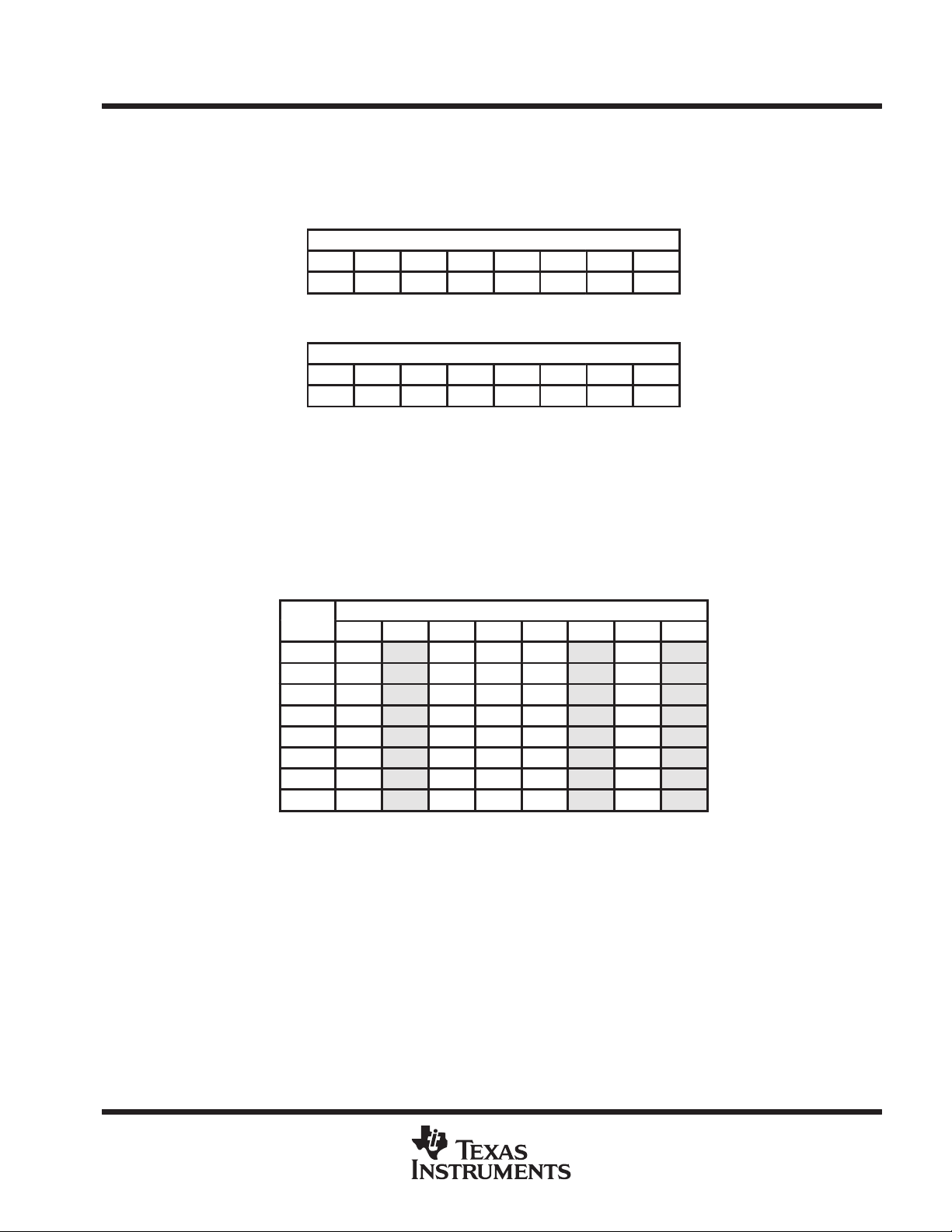
ThunderSWITCH II
9-PORT 100-/1000-MBIT/S ETHERNET SWITCH
SPWS044E – DECEMBER 1997 – REVISED AUGUST 1999
TNETX4090
port trunking example
This example shows how to set up the TNETX4090 to support two port trunks. The first trunk group consists
of ports 1, 3, 5, and 7 (see Table 21); the second trunk group consists of ports 0, 2, and 6 (see Table 22).
Table 21. Trunk Group 0 Port Membership (Trunk0Ports Register)
PORT
7 6 5 4 3 2 1 0
1 0 1 0 1 0 1 0
Table 22. Trunk Group 1 Port Membership (Trunk1Ports Register)
PORT
7 6 5 4 3 2 1 0
0 1 0 0 0 1 0 1
The TrunkMapx registers are used to control the distribution of traffic across the ports within a trunk group. In
this example, the traffic for trunk group 0 has been equally distributed 25% (this assumes that bits 3–1 of the
MAC addresses are random enough to give an even distribution) for each of the four ports in the trunk. For any
given source and destination address pair, the traf fic always uses the same port within the trunk. This ensures
that packets do not get disordered on the trunk ports. Note that, since port 4 is not a member of any port trunk
group, all the entries for this port have been set to 1. In fact, functionally , this can be thought of as a single port
trunk.
Table 23. TrunkMapx Register Settings (for Traffic Distribution on Trunk Groups 0 and 1)
MAP
INDEX
0 0 1 0 1 0 0 1 0
1 0 0 0 1 1 1 0 0
2 0 0 1 1 0 0 0 1
3 1 1 0 1 0 0 0 0
4 0 0 0 1 0 1 1 0
5 0 0 0 1 1 0 0 1
6 0 1 1 1 0 0 0 0
7 1 0 0 1 0 1 0 0
7 6 5 4 3 2 1 0
TRUNK PORT
extended port awareness
When the port routing code is derived from an xportcode field, which has its most significant bit set (1xxxxx)
indicating a port on an external crossbar matrix connected to port 8, the port-8 bit in the port routing code is set,
and the five least significant bits of xportcode are used to create the pretag transmitted with the frame.
When bit 8 of the port routing code is set by a portvector field, the xroutecode field associated with the portvector
is used to create the pretag transmitted with the frame (either directly if xroutecode is in the range
000000–010000, or indirectly via a lookup in the XMultiGroup17–XMulUGroup63 registers if xroutecode is in
the range 010001–111111).
POST OFFICE BOX 655303 • DALLAS, TEXAS 75265
55
Page 56

TNETX4090
ThunderSWITCH II
9-PORT 100-/1000-MBIT/S ETHERNET SWITCH
SPWS044E – DECEMBER 1997 – REVISED AUGUST 1999
flow control
The TNETX4090 supports collision-based flow control for ports in half-duplex mode and IEEE Std 802.3x flow
control for ports in full-duplex mode. The flow bit in the SysControl register determines the action that will be
taken when back pressure is needed, that is, when there are insufficient resources to handle an inbound packet.
The holb bit in the SysControl register determines when back pressure is needed.
D
If flow = 0, packets are discarded at the ingress port when insufficient resources are available to handle
them.
D
If flow = 1, ports in half-duplex mode cause collisions to avoid accepting packets, ports in full-duplex mode
whose link partners negotiated to accept pause packets will send them; otherwise, packets are dropped.
If port 8 is in MII mode, the pause-frame transmission/reception is required to be symmetrical. If in GMII or
PMA mode, transmit and receive pause capabilities are negotiated independently.
D
With holb = 0, back pressure is applied to all ports when the number of buffers in the global pool is down
to the value in the FlowThreshold register (or half of this value if the packet arrives at a port in gigabit mode).
This prevents the reception of more frames at any port until the frame backlog is reduced and the number
of free buffers has risen above the threshold. When this happens, back pressure is removed from all ports
and packets can be received. The value in FlowThreshold should be set so that all ports can complete
reception of a maximum-size frame, that is, each port should have enough time to activate the flow
mechanisms without dumping a frame for which reception has started.
D
If holb = 1, back pressure is applied as when holb = 0, or to an individual port when the buffers held in
memory for data that arrived on that port is greater than the available pool remaining. Assume that
FlowThreshold is set small enough that this mechanism does not affect the back pressure in this mode. An
example is:
– When port A’ s traffic begins to backlog in memory [no matter to what port(s) it is destined], back pressure
will be applied when the amount of data backed up is greater than the available pool (about half the
buffers are assigned to data from port A). If A ’s data stays backlogged and if data arriving at port B also
begins to backlog in memory , back pressure will be applied to port B when its data amounts to one-fourth
of the buffer pool, or half of the half left after port A had back pressure applied. When port A’s traffic
begins to exit the switch, port A will stay back pressured until its data is equal to one third of the total. As
buffers become available, port B will be allowed to consume up to one third of the buffer pool (each
backlogged total is compared with the buffers available). In this mode, only the stations that have
caused their fair share of buffers to be removed from the available pool will be back pressured.
Setting holb = 1 activates circuitry that attempts to prevent a backlogged conversation stalling other port
traffic by using up all the memory buffers. Because the number of buffers charged to a particular port is
always compared with the number of buffers left, there is no threshold register for this mode.
56
POST OFFICE BOX 655303 • DALLAS, TEXAS 75265
Page 57

ThunderSWITCH II
other flow-control mechanisms
hardware flow control
If a port were in MII or GMII mode and full duplex, normally , its Mxx_COL would not be needed. Hardware flow
control has been added by preventing the start of a frame transmission if the Mxx_COL is high. This is useful
in ring mode; the Mxx_COL can be tied to the FLOW of the upstream neighbor for hardware flow control.
multicast limit
Because buffer resources for multicast (or broadcast) frames are released only when the last port has
transmitted the frame, multicast packets to fast and slow ports are released at the slow-port rate. Multicast traffic
from a fast port to a slow port could cause back pressure to be applied to the source port, blocking input from
that port. This occurs even if at least one of the ports in the multicast could have kept pace with the inbound
multicast packets. The MCastLimit register can limit the number of multicast packets allowed to be pending at
any output port. When the limit is reached, that port is not added to the routing vector of the next multicast packet
for which it was eligible. Eligibility is restored when the number of backlogged packets is again below the limit.
MCastLimit allows the user to set the ports subject to this restriction, and set the limit in 8 binary steps, from
2 to 256. The spanning-tree BPDU multicast packet is exempt from this limit.
other behavior changes resulting from flow-control bits or terminals
Clearing (the default) holbrm in the RingPorts register includes the test for buffer use controlled by the holb bit
in SysControl into the action of the FLOW terminal. FLOW goes high if either the number of buffers left is less
than the FlowThreshold value or a ring-mode port receive operation has exceeded its fair share of buffers.
Setting holbrm = 1 makes FLOW respond only to FlowThreshold value violations.
9-PORT 100-/1000-MBIT/S ETHERNET SWITCH
SPWS044E – DECEMBER 1997 – REVISED AUGUST 1999
TNETX4090
system test capabilities
RDRAM
The external RDRAM can be read and written using regular DIO accesses following a stop. Individual bytes can
be read and written. However, as the RDRAM memory is actually accessed in 128-byte pages, performing
128-byte accesses is the most efficient.
T o access the RDRAM, the TNETX4090 must not be operating. The user must perform a reset and not set start
in SysControl. Both start and initd in SysControl must be 0. In addition, rdinit in SysT est must be set, indicating
that the RDRAM has initialized. This initialization sequence occurs automatically after a hard reset.
Read or write accesses to RDRAM are invoked via rdram and rdwrite in SysTest. Setting rdram to 1 causes a
128-byte transfer between the device and the RDRAM memory to be initiated.
D
The transfer direction is determined by rdwrite.
D
The external memory byte address for the access is specified by ramaddress in RAMAddress.
D
Data to be read from or written to RDRAM is accessed indirectly via RAMData.
writing RDRAM
Writing to RDRAM memory is accomplished as follows:
1. Write the byte address for the access to ramaddress in RAMAddress.
2. Write the data for the access to RAMData. Up to 64 bytes can be written, if all but the six least significant
bits of the address are the same for all the data. Inc in RAMAddress can be used to autoincrement the
address.
3. Set rdwrite = 0 and rdram = 1 (these can be written simultaneously).
4. If required, poll rdram until it becomes 0. This indicates that the write has completed.
POST OFFICE BOX 655303 • DALLAS, TEXAS 75265
57
Page 58

TNETX4090
ThunderSWITCH II
9-PORT 100-/1000-MBIT/S ETHERNET SWITCH
SPWS044E – DECEMBER 1997 – REVISED AUGUST 1999
reading RDRAM
Reading from RDRAM memory is accomplished as follows:
1. Write the byte address for the access to ramaddress in RAMAddress.
2. Set rdwrite = 1 and rdram = 1 (these can be written simultaneously).
3. Poll rdram until it becomes 0. This indicates that the read has completed.
4. Read the data for the access to RAMData. Up to 64 bytes can be read, provided that all but the six least
significant bits of the address are the same for all the data. Inc in RAMAddress can be used to autoincrement
the address.
internal wrap test
Internal wrap mode causes some or all of the Ethernet MACs to be configured to loop back transmitted data
into the receive path. This allows a frame to be sent into a designated source port and then selectively routed
successively to and from ports involved in the test, before finally transmitting the frame out of the original port.
By varying the number of ports between which the frame is forwarded, the potential fault capture area is
expanded or constrained.
Intwrap in SysT est determines which ports loop back. Ports 0 or 8 can be configured to not loop back, allowing
them to be used as the start/end port for the test. Alternatively, the NM port (accessed via DIO) can be used
for this purpose, with all MII ports configured to loop back.
For a frame to be forwarded from one port to another in this fashion, the switch must be programmed as follows:
D
Assign a unique VID to each of the PortxQTag registers, and program these tags into the VLANnQID
registers.
D
The VLANnPorts register associated with each of the VLANnQID registers should have only one bit set,
indicating to which port frames containing that IEEE Std 802.3 tag should be routed.
D
Rxacc and Txacc for each port must be 1. This causes the port to add the VID from its PortxQTag to the
frame on reception, and strip the tag before transmission.
D
The destination address of the frames to be applied is not known, and UnkUniPorts and UnkMultiPorts
should be all 1s.
This causes the following:
1. The VID from the source port PortxQTag register is added to the frame upon reception. As the address of
the frame is unknown, it is forwarded to the AND of the appropriate VLANnPorts and UnkUniPorts (unicast)
or UnkMultiPorts (multicast). As VLANnPorts should contain only a single 1, this should be a single port.
2. The frame is transmitted from the destination port selected in 1. Its VLAN tag is stripped beforehand; the
frame loops back to the receive path.
3. Steps 1 and 2 are repeated, but the VID added upon reception is different from the one just stripped off at
transmission. This means a different VLANnPorts register is used to determine the destination.
The port order shown here is sequential, but the actual order depends on how ports are paired in the
VLANnPorts registers, and how the PortxQTag registers are assigned.
4. Eventually, the frame is sent to a port that is not configured for loopback, and leaves the switch.
58
POST OFFICE BOX 655303 • DALLAS, TEXAS 75265
Page 59

ThunderSWITCH II
internal wrap test (continued)
08
07
TNETX4090
9-PORT 100-/1000-MBIT/S ETHERNET SWITCH
SPWS044E – DECEMBER 1997 – REVISED AUGUST 1999
06
05
04 03 02 01 00
TNETX4090
NM
Figure 13. Internal Wrap Example
The operational status of the PHYs or external connections to the device do not have to be considered or
assumed good, when in internal loopback mode.
duplex wrap test
Duplex wrap test is similar to internal wrap mode (see Figure 13). The ports can be set to accept frame data
that is wrapped at the PHY. This permits network connections between the device and the PHY to be verified.
Any port can be the source port (not just the NM port as shown in Figure 14). By using multicast/broadcast
frames, traffic can be routed selectively between ports involved in the test or return the frame directly before
retransmission on the uplink. Software control of the external PHYs is required to configure them for loopback.
If the internal PCS is in use (port configured in PMA mode) loopback in PCSxControl also must be asserted.
This causes Mxx_EWRAP to be high, forcing external PMD into loopback mode.
Duplex frame-wrap test mode is selected by setting dpwrap in SysTest. When selected, the port is forced into
full duplex, allowing it to receive frames it transmits.
The switch is configured in the same manner as internal wrap.
08
PHY
PHY
07
06
05
04 03 02 01 00
TNETX4090
Figure 14. Duplex Wrap Example
POST OFFICE BOX 655303 • DALLAS, TEXAS 75265
NM
59
Page 60

TNETX4090
ThunderSWITCH II
9-PORT 100-/1000-MBIT/S ETHERNET SWITCH
SPWS044E – DECEMBER 1997 – REVISED AUGUST 1999
absolute maximum ratings over operating free-air temperature range (unless otherwise noted)
Supply voltage range, V
Supply voltage range, V
Supply voltage range, V
DD(2.5)
DD(3.3)
DD
(see Note 1) –0.5 V to 2.7 V. . . . . . . . . . . . . . . . . . . . . . . . . . . . . . . . . . . . . . . . .
(see Note 1) –0.5 V to 3.6 V. . . . . . . . . . . . . . . . . . . . . . . . . . . . . . . . . . . . . . . . .
a (see Note 1) –0.5 V to 2.7 V. . . . . . . . . . . . . . . . . . . . . . . . . . . . . . . . . . . . . . . . . . . .
†
Supply voltage range, DVREF (see Note 1) 1 V to 2.2 V. . . . . . . . . . . . . . . . . . . . . . . . . . . . . . . . . . . . . . . . . . . . .
Input voltage range, VI –0.5 V to V
Output voltage range, VO –0.5 V to V
DD(3.3)
DD(3.3)
+ 0.4 V. . . . . . . . . . . . . . . . . . . . . . . . . . . . . . . . . . . . . . . . . . . . . . . . . . .
+ 0.5 V. . . . . . . . . . . . . . . . . . . . . . . . . . . . . . . . . . . . . . . . . . . . . . . .
Input voltage range (RSL), VIR DVREF – 0.35 to DVREF + 0.8. . . . . . . . . . . . . . . . . . . . . . . . . . . . . . . . . . . . . .
Output voltage range (RSL), V
Thermal impedance, junction-to-ambient package, Z
0.0 to V
. . . . . . . . . . . . . . . . . . . . . . . . . . . . . . . . . . . . . . . . . . . . . . . . . . .
OR
:Airflow = 0 11.11°C/W. . . . . . . . . . . . . . . . . . . . . . . . .
θJA
DD(2.5)
Airflow = 100 ft/min 9.61°C/W. . . . . . . . . . . . . . . . .
Thermal impedance, junction-to-case package, Z
Operating case temperature range, T
Storage temperature range, T
†
Stresses beyond those listed under “absolute maximum ratings” can cause permanent damage to the device. These are stress ratings only, and
functional operation of the device at these or any other conditions beyond those indicated under “recommended operating conditions” is not
implied. Exposure to absolute-maximum-rated conditions for extended periods can affect device reliability.
NOTE 1: All voltage values are with respect to GND.
stg
0°C to 70°C. . . . . . . . . . . . . . . . . . . . . . . . . . . . . . . . . . . . . . . . . . . . . . . .
C
–65°C to 150°C. . . . . . . . . . . . . . . . . . . . . . . . . . . . . . . . . . . . . . . . . . . . . . . . . . .
0.94°C/W. . . . . . . . . . . . . . . . . . . . . . . . . . . . . . . . . . . . . .
θJC
recommended operating conditions
MIN NOM MAX UNIT
V
DD(2.5)
V
DD(3.3)
DVREF RSL reference voltage 1.8 2.0 2.2 V
V
I
V
O
V
IH
V
IL
I
OH
I
OL
I
OL
V
IHR
V
ILR
I
OHR
I
OLR
NOTE 2: The algebraic convention, in which the more-negative (less-positive) limit is designated as a minimum, is used for logic-voltage levels
Supply voltage 2.5 2.6 2.7 V
Supply voltage 3 3.3 3.6 V
Input voltage 0 V
Output voltage 0 V
High-level input voltage 2 V
Low-level input voltage (see Note 2) 0 0.8 V
High-level output current –2 mA
Low-level output current (except LED_DATA) 2 mA
LED_DATA (terminal AE19) 0 8 mA
High-level input voltage (RSL) DVREF+0.35 DVREF+0.8 V
Low-level input voltage (RSL) (see Note 2) DVREF–0.35 DVREF–0.8 V
High-level output current (RSL) –10 10 µA
Low-level output current (RSL) 0 80 mA
only.
DD(3.3)
DD(3.3)
DD(3.3)
V
V
V
60
POST OFFICE BOX 655303 • DALLAS, TEXAS 75265
Page 61

ThunderSWITCH II
9-PORT 100-/1000-MBIT/S ETHERNET SWITCH
SPWS044E – DECEMBER 1997 – REVISED AUGUST 1999
TNETX4090
electrical characteristics over recommended operating conditions (unless otherwise noted)
PARAMETER TEST CONDITIONS MIN TYP MAX UNIT
V
OH
V
OL
I
OZ
I
IH
I
IL
V
OHR
V
OLR
I
DD(2.5V)
I
DD(3.3V)
I
DD(2.5)
C
i
C
o
High-level output voltage IOH = rated V
Low-level output voltage IOL = rated 0.5 V
High-impedance-state output
current
High-level input current VI = V
Low-level input current VI = V
High-level output voltage (RSL) I
Low-level output voltage (RSL) 0 0.4 V
Supply current
Capacitance, input 6 pF
Capacitance, output 6 pF
VO = VDD or GND ±10 µA
IH
IL
OH
V
DD(2.5V)
DTX_CLK and DRX_CLKf = 83.33 MHz
V
DD(3.3V)
DTX_CLK and DRX_CLKf = 83.33 MHz
V
DD(2.5)
DTX_CLK and DRX_CLKf = 83.33 MHz
= max,
= max,
= max,
–0.5 V
DD(3.3)
2 V
1 µA
–1 µA
DD
1.5
0.5
0.175
V
A
timing requirements over recommended operating conditions
JTAG interface
control signals
RESET (see Figure 15)
NO. MIN MAX UNIT
1 t
1 t
w(RESETP)
w(RESET)
RESET
Pulse duration, RESET low at power up 100 µs
Pulse duration, RESET low at other times 4 t
1
Figure 15. RESET
cycle
POST OFFICE BOX 655303 • DALLAS, TEXAS 75265
61
Page 62

TNETX4090
ThunderSWITCH II
9-PORT 100-/1000-MBIT/S ETHERNET SWITCH
SPWS044E – DECEMBER 1997 – REVISED AUGUST 1999
physical medium attachment interface (port 8)
receive
PMA receive (see Figure 16)
NO. MIN MAX UNIT
1 t
c(Mxx_RBC)
– t
drift(Mxx_RBC)
2,3 t
w(Mxx_RBC)
4 t
su(Mxx_RXD)
4 t
su(Mxx_RXDV)
4 t
su(Mxx_RXER)
5 t
h(Mxx_RXD)
5 t
h(Mxx_RXDV)
5 t
h(Mxx_RXER)
6 t
†
skew(Mxx_RBC)
t
is the (minimum) time for either RBC0 or RBC1 to drift from 63.5 MHz to 64.5 MHz or 60 Mhz to 59 MHz from their lock value. It is applicable
drift
under all input signal conditions (except under certain circumstances during comma detection), including invalid or absent input signals, if the
receiver clock recovery unit was previously locked to Mxx_RFCLK or to a valid input signal.
Cycle time, receive byte clock 0 and 1 (Mxx_RCLK, Mxx_COL) 16 16 ns
Drift rate† of receive bye clock 0 and 1 0.2 ns
Pulse duration, Mxx_RCLK, Mxx_COL low or high 40% 60% ns
Setup time, Mxx_RXD7–Mxx_RXD0 valid before Mxx_RCLK/COL↑ 2.5 ns
Setup time, Mxx_RXDV valid before Mxx_RCLK/COL↑ 2.5 ns
Setup time, Mxx_RXER valid before Mxx_RCLK/COL↑ 2.5 ns
Hold time, Mxx_RXD7–Mxx_RXD0 valid after Mxx_RCLK/COL↑ 1.5 ns
Hold time, Mxx_RXDV valid after Mxx_RCLK/COL↑ 1.5 ns
Hold time, Mxx_RXER valid after Mxx_RCLK/COL↑ 1.5 ns
Skew between receive byte clock 1 and receive byte clock 0 7.5 8.5 ns
Receive Byte
Clock 0
Receive
Code Group
Comma Detect
Receive Byte
Clock 0
1
6
2 5
3
4
Figure 16. PMA Receive
4
5
Data Group
62
POST OFFICE BOX 655303 • DALLAS, TEXAS 75265
Page 63

ThunderSWITCH II
9-PORT 100-/1000-MBIT/S ETHERNET SWITCH
SPWS044E – DECEMBER 1997 – REVISED AUGUST 1999
TNETX4090
transmit
PMA transmit (see Figure 17)
NO. MIN MAX UNIT
†
1 t
c(Mxx_GTCLK)
2,3 t
w(Mxx_GTCLK)
4 t
su(Mxx_TXD)
4 t
su(Mxx_TXEN)
4 t
su(Mxx_TXER)
5 t
h(Mxx_TXD)
5 t
h(Mxx_TXDV)
5 t
†
h(Mxx_TXER)
±100-ppm tolerance
Transmit
Code Group
Cycle time, Mxx_GTCLK 8
Pulse duration, Mxx_GTCLK low or high 40% 60% t
Setup time, Mxx_RXD7–Mxx_RXD0 valid before Mxx_GTCLK↑ 2 ns
Setup time, Mxx_RXDV valid before Mxx_GTCLK↑ 2 ns
Setup time, Mxx_RXER valid before Mxx_GTCLK↑ 2 ns
Hold time, Mxx_RXD7–Mxx_RXD0 valid after Mxx_GTCLK↑ 1 ns
Hold time, Mxx_RXDV valid after Mxx_GTCLK↑ 1 ns
Hold time, Mxx_RXER valid after Mxx_GTCLK↑ 1 ns
1
3
42
5
†
8
c(Mxx_GTCLK)
ns
Transmit
Clock
Figure 17. PMA Transmit
POST OFFICE BOX 655303 • DALLAS, TEXAS 75265
63
Page 64

TNETX4090
ThunderSWITCH II
9-PORT 100-/1000-MBIT/S ETHERNET SWITCH
SPWS044E – DECEMBER 1997 – REVISED AUGUST 1999
GMII (port 8)
Figures 18–20 show the timing for the 100-/1000-Mbit/s GMII when operating at 1000 Mbit/s.
Both Mxx_CRS and Mxx_COL are driven asynchronously by the PHY. Mxx_RXD7–MxxRXD0 is driven by the
PHY on the falling edge of Mxx_RCLK. Mxx_RXD7–MxxRXD0 timing must be met during clock periods in which
Mxx_RXDV is asserted. Mxx_RXDV is asserted and deasserted by the PHY on the falling edge of Mxx_RCLK.
Mxx_RXER is driven by the PHY on the falling edge of Mxx_RCLK.
GMII receive (see Figure 18)
NO. MIN MAX UNIT
1 t
su(Mxx_RXD)
1 t
su(Mxx_RXDV)
1 t
su(Mxx_RXER)
2 t
h(Mxx_RXD)
2 t
h(Mxx_RXDV)
2 t
h(Mxx_RXER)
Mxx_RCLK
Setup time, Mxx_RXD7–Mxx_RXD0 valid before Mxx_RCLK↑ 2 ns
Setup time, Mxx_RXDV valid before Mxx_RCLK↑ 2 ns
Setup time, Mxx_RXER valid before Mxx_RCLK↑ 2 ns
Hold time, Mxx_RXD7–Mxx_RXD0 valid after Mxx_RCLK↑ 1 ns
Hold time, Mxx_RXDV valid after Mxx_RCLK↑ 1 ns
Hold time, Mxx_RXER valid after Mxx_RCLK↑ 1 ns
1 2
Mxx_RXD7–Mxx_RXD0
Mxx_RXDV
Mxx_RXER
Figure 18. GMII Receive
Mxx_CRS and Mxx_COL are driven asynchronously by the PHY. Mxx_GTCLK is derived directly from
Mxx_RFCLK. Mxx_TXD7–Mxx_TXD7 is driven by the reconciliation sublayer synchronous to the Mxx_GTCLK.
Mxx_TXEN is asserted and deasserted by the reconciliation sublayer synchronous to the Mxx_GTCLK rising
edge. Mxx_TXER is driven synchronous to the rising edge of Mxx_GTCLK.
GMII transmit (see Figure 19)
NO. MIN MAX UNIT
1 t
d(Mxx_TXD)
1 t
d(Mxx_TXEN)
1 t
d(Mxx_TXER)
Mxx_GTCLK
Mxx_TXD7–Mxx_TXD0
Mxx_TXEN
Mxx_TXER
Delay time, from Mxx_GTCLK↑ to Mxx_TXD3–MxxTXD0 valid 1.5 4.5 ns
Delay time, from Mxx_GTCLK↑ to Mxx_TXEN valid 1.5 4.5 ns
Delay time, from Mxx_GTCLK↑ to Mxx_TXER valid 1.5 4.5 ns
1
64
Figure 19. GMII Transmit
POST OFFICE BOX 655303 • DALLAS, TEXAS 75265
Page 65

ThunderSWITCH II
9-PORT 100-/1000-MBIT/S ETHERNET SWITCH
SPWS044E – DECEMBER 1997 – REVISED AUGUST 1999
TNETX4090
PMA and GMII clock (see Figure 20)
NO. MIN MAX UNIT
1 t
2 t
3 t
r(Mxx_GCLK)
h(Mxx_GCLK)
w(Mxx_GCLK)
Pulse width low, Mxx_RFCLK 2.5 ns
Pulse width high, Mxx_RFCLK 2.5 ns
Cycle time, Mxx_RFCLK 8 ns
PMA and GMII clock (see Figure 20)
NO. MIN MAX UNIT
1 t
r(Mxx_GCLK)
2 t
f(Mxx_GCLK)
3 Accuracy 100 PPM
duty cycle 40% 60%
†
tr and tf are measured between 20% and 80%, V
Mxx_RFCLK
Rise time, Mxx_RFCLK 1 ns
Fall time, Mxx_RFCLK 1 ns
DD(3.3-V)
= min, output load (GTCLK) = 20pf.
3
1 2
Figure 20. GMII Clock
POST OFFICE BOX 655303 • DALLAS, TEXAS 75265
65
Page 66

TNETX4090
ThunderSWITCH II
9-PORT 100-/1000-MBIT/S ETHERNET SWITCH
SPWS044E – DECEMBER 1997 – REVISED AUGUST 1999
MII (ports 0–8)
Figures 21–23 show the timing for the eight MIIs operating at either 10-Mbit/s or 100-Mbit/s, and the GMII
operating at 100-Mbit/s.
Mxx_CRS and Mxx_COL are driven asynchronously by the PHY . Mxx_RXD3–Mxx_RXD0 is driven by the PHY
on the falling edge of Mxx_RCLK. Mxx_RXD3–Mxx_RXD0 timing must be met during clock periods in which
Mxx_RXDV is asserted. Mxx_RXDV is asserted and deasserted by the PHY on the falling edge of Mxx_RCLK.
Mxx_RXER is driven by the PHY on the falling edge of Mxx_RCLK.
MII receive (see Figure 21)
NO. MIN MAX UNIT
1 t
su(Mxx_RXD)
1 t
su(Mxx_RXDV)
1 t
su(Mxx_RXER)
2 t
h(Mxx_RXD)
2 t
h(Mxx_RXDV)
2 t
h(Mxx_RXER)
Setup time, Mxx_RXD3–Mxx_RXD0 valid before Mxx_RCLK↑ 8 ns
Setup time, Mxx_RXDV valid before Mxx_RCLK↑ 8 ns
Setup time, Mxx_RXER valid before Mxx_RCLK↑ 8 ns
Hold time, Mxx_RXD3–Mxx_RXD0 valid after Mxx_RCLK↑ 8 ns
Hold time, Mxx_RXDV valid after Mxx_RCLK↑ 8 ns
Hold time, Mxx_RXER valid after Mxx_RCLK↑ 8 ns
1 2
Mxx_RCLK
Mxx_RXD3–Mxx_RXD0
Mxx_RXDV
Mxx_RXER
Figure 21. MII Receive
NOTE: For port 8, M08_RFCLK is used for the transmit clock input.
Mxx_CRS and Mxx_COL are driven asynchronously by the PHY. Mxx_TXD3–Mxx_TXD0 is driven by the
reconciliation sublayer synchronous to Mxx_TCLK. Mxx_TXEN is asserted and deasserted by the reconciliation
sublayer synchronous to the Mxx_TCLK rising edge. Mxx_TXER is driven synchronous to the rising edge of
Mxx_TCLK.
66
POST OFFICE BOX 655303 • DALLAS, TEXAS 75265
Page 67

ThunderSWITCH II
9-PORT 100-/1000-MBIT/S ETHERNET SWITCH
SPWS044E – DECEMBER 1997 – REVISED AUGUST 1999
TNETX4090
MII transmit (see Figure 22)
NO. MIN MAX UNIT
1 t
1 t
1 t
d(Mxx_TXD)
d(Mxx_TXEN)
d(Mxx_TXER)
Mxx_TCLK
Delay time, from Mxx_TCLK↑ to Mxx_TXD3–MxxTXD0 valid 5 15 ns
Delay time, from Mxx_TCLK↑ to Mxx_TXEN valid 5 15 ns
Delay time, from Mxx_TCLK↑ to Mxx_TXER valid 5 15 ns
1
Mxx_TXD3–Mxx_TXD0
Mxx_TXEN
Mxx_TXER
Figure 22. MII Transmit
MII clock (see Figure 23)
NO. MIN MAX UNIT
1 t
2 t
3 t
r(Mxx_CLK)
h(Mxx_CLK)
w(Mxx_CLK)
Mxx_RCLK
Mxx_TCLK
Pulse width low Mxx_RCLK, Mxx_TCLK 35% 65%
Pulse width high Mxx_RCLK, Mxx_TCLK 35% 65%
Cycle time Mxx_RCLK, Mxx_TCLK 2.5 25 MHz
3
1 2
Figure 23. MII Clock
POST OFFICE BOX 655303 • DALLAS, TEXAS 75265
67
Page 68

TNETX4090
ThunderSWITCH II
9-PORT 100-/1000-MBIT/S ETHERNET SWITCH
SPWS044E – DECEMBER 1997 – REVISED AUGUST 1999
RDRAM interface
RDRAM (see Figure 24)
NO. MIN MAX UNIT
1 t
c(DX_CLK)
2, 3 t
w(DX_CLK)
4, 5 t
w(TICK)
6, 8 t
su(DBUS_DATA)
7, 9 t
h(DBUS_DATA)
10, 11 t
†
d(DBUS_OUT)
†
t
cycle
Not shown in Figure 24 due to scale
DTX_CLK
DRX_CLK
Cycle time DTX_CLK, DRX_CLK 3.33 3.33 ns
Pulse duration, DTX_CLK, DRX_CLK low or high 45% 55% t
Pulse duration, tick time 0.5 0.5 t
Setup time, DBUS_DA TA before tick 0.35 ns
Hold time, DBUS_DATA after tick 0.35 ns
Delay time, DBUS_DATA, DBUS_CTRL, DBUS_EN from tick 0.635 1.438 t
Cycle time, internal clock 4 t
1
2 3
4 5
10 11
6 7 8 9
c(DX_CLK)
c(DX_CLK)
c(DX_CLK)
cycle
DBUS_DATA (in)
DBUS_CTRL
DBUS_EN
DBUS_DATA (out)
Figure 24. RDRAM
68
POST OFFICE BOX 655303 • DALLAS, TEXAS 75265
Page 69

ThunderSWITCH II
9-PORT 100-/1000-MBIT/S ETHERNET SWITCH
SPWS044E – DECEMBER 1997 – REVISED AUGUST 1999
TNETX4090
DIO interface
The DIO interface is simple and asynchronous to allow easy adaptation to a range of microprocessor devices
and computer system interfaces.
DIO and DMA writes (see Figure 25)
NO. MIN MAX UNIT
1 t
w(SCS)
2 t
su(SRNW)
3 t
su(SAD)
4 t
su(SDATA)
5 t
h(SRNW)
6 t
h(SAD)
7 t
h(SDATA)
8 t
h(SCSL)
9 t
d(SRDYZH)
10 t
d(SRDYHL)
11 t
d(SRDYLH)
12 t
h(SCSH)
13 t
w(SRDY)
14 t
†
d(SINT)
When the switch is performing certain internal operations (e.g., EEPROM load), there is a delay of up to 20 ms (24C02) or 800 ms (24C08)
between SCS
being asserted and SRDY being asserted.
Pulse duration, SCS↓ 2t
Setup time, SRNW valid before SCS↓ 0 ns
Setup time, SAD1–SAD0, SDMA valid before SCS↓ 0 ns
Setup time, SAD7–SAD0 valid before SCS↓ 0 ns
Hold time, SRNW low after SRDY↓ 0 ns
Hold time, SAD1–SAD0, SDMA valid after SRDY↓ 0 ns
Hold time, SAD7–SAD0 valid after SRDY↓ 0 ns
Hold time, SCS low after SRDY↓ 0 ns
Delay time from SCS↓ to SRDY↑ 10 ns
Delay time from SCS↓ to SRDY↓ 2t
Delay time from SCS↑ to SRDY↑ tc2tc+10 ns
Hold time, SCS high after SRDY↑ 0 ns
Pulse duration, SRDY↑ t
Delay time from SRDY↓ to SINT valid. (write to INT or INT_Enable register) 2t
c
c
ns
†
ns
ns
c
ns
c
SCS
SRNW
SAD1–SAD0
SDMA
SDATA7–
SDATA0
SRDY
SINT
4 10
3
2 9
Figure 25. DIO and DMA Writes
1
8 11 12
5
6
7
13
14
POST OFFICE BOX 655303 • DALLAS, TEXAS 75265
69
Page 70

TNETX4090
ThunderSWITCH II
9-PORT 100-/1000-MBIT/S ETHERNET SWITCH
SPWS044E – DECEMBER 1997 – REVISED AUGUST 1999
DIO and DMA reads (see Figure 26)
NO. MIN MAX UNIT
1 t
w(SCSL)
2 t
su(SRNW)
3 t
su(SAD)
4 t
h(SRNW)
5 t
h(SAD)
6 t
h(SCSL)
7 t
su(SDATAD)
8 t
d(SRDYZH)
9 t
d(SRDYHL)
10 t
d(SDATAZ)
11 t
d(SRDYLH)
12 t
h(SCSH)
13 t
†
w(SRDY)
When the switch is performing certain internal operations (e.g., EEPROM load), there is a delay of up to 20 ms (24C02) or 800 ms (24C08)
between SCS
being asserted and SRDY being asserted.
Pulse duration, SCS low 2t
Setup time, SRNW valid before SCS↓ 0 ns
Setup time, SAD1–SAD0, SDMA valid before SCS↓ 0 ns
Hold time, SRNW low after SRDY↓ 0 ns
Hold time, SAD1–SAD0, SDMA valid after SRDY↓ 0 ns
Hold time, SCS low after SRDY↓ 0 ns
Setup time from SRDY↓ to SDATA7–SDATA0 driven 0 ns
Delay time from SCS↓ to SRDY↑ 10 ns
Delay time from SCS↓ to SRDY↓ 0
Delay time from SCS↑ to SDATA7–SDATA0 3-state 0 10 ns
Delay time from SCS↑ to SRDY↑ tc2tc+10 ns
Hold time, SCS high after SRDY↑ 0 ns
Pulse duration, SRDY high t
c
†
c
ns
ns
ns
SCS
SRNW
SAD1–SAD0
SDMA
SDATA7–
SDATA0
SRDY
3
2 8
1
9
7
Figure 26. DIO and DMA Reads
11
6 10 12
4
5
13
70
POST OFFICE BOX 655303 • DALLAS, TEXAS 75265
Page 71
ThunderSWITCH II
9-PORT 100-/1000-MBIT/S ETHERNET SWITCH
SPWS044E – DECEMBER 1997 – REVISED AUGUST 1999
TNETX4090
EEPROM interface
For further information on EEPROM interface timing, refer to the 24C02 or 24C08 serial EEPROM data sheets.
EEPROM writes (see Figure 27)
NO. MIN MAX UNIT
1 t
su(EDIO:Start)
2 t
h(EDIO:Start)
3 t
h(EDIO:Data)
4 t
su(EDIO:Data)
5 t
w(ECLK)
6 t
w(ECLK)
7 t
w(ECLK:Data)
8 t
w(ECLK:Data)
9 f
clock(ECLK)
EDIO (out)
Setup time, start condition during ECLK high 383 t
Hold time, start condition during ECLK high 383 t
Hold time, data after ECLK↓ 0 t
Setup time, data before ECLK↑ 383 t
Pulse duration, ECLK low during start/stop 766 t
Pulse duration, ECLK high during start/stop 766 t
Pulse duration, ECLK high during data 383 t
Pulse duration, ECLK low during data 766 t
Clock frequency, ECLK 98 kHz
3
421
c
c
c
c
c
c
c
c
5 6
ECLK
7 8
Figure 27. EEPROM Writes
EEPROM reads (see Figure 28)
NO. MIN MAX UNIT
1 t
2 t
ECLK
EDIO (in)
su(EDIO)
h(EDIO)
Setup time, EDIO (in) before ECLK↑ 10 ns
Hold time, EDIO (in) after ECLK↓ 0 ns
1
2
Figure 28. EEPROM Reads
POST OFFICE BOX 655303 • DALLAS, TEXAS 75265
71
Page 72

TNETX4090
ThunderSWITCH II
9-PORT 100-/1000-MBIT/S ETHERNET SWITCH
SPWS044E – DECEMBER 1997 – REVISED AUGUST 1999
LED interface
LED (see Figure 29)
NO. MIN MAX UNIT
1 t
c(LED_CLK)
2 t
w(LED_CLK)
3 t
n(LED_CLK)
4 t
c(BURST)
5 t
su(LED_DATA
6 t
†
‡
h(LED_DATA)
During hard reset, LED_CLK runs continuously.
Does not apply during hard reset
LED_CLK
Cycle time, LED_CLK 8 t
Pulse duration, LED_CLK high 4 t
Number of LED_CLK pulses in burst 24
Cycle time, LED_CLK burst 4687488
Setup time, LED_DATA before LED_CLK↑ 4 t
)
Hold time, LED_DATA after LED_CLK↑ 4 t
4
3
1
6
2
5
†
‡
c
c
t
c
c
c
LED_DATA
First LED Second LED Last LED First LED
Figure 29. LED
72
POST OFFICE BOX 655303 • DALLAS, TEXAS 75265
Page 73

ThunderSWITCH II
9-PORT 100-/1000-MBIT/S ETHERNET SWITCH
SPWS044E – DECEMBER 1997 – REVISED AUGUST 1999
TNETX4090
PARAMETER MEASUREMENT INFORMATION
The following load circuits and voltage waveforms show the conditions used for measuring switching characteristics.
T est points are illustrated schematically on the load circuits. Reference points are plotted on the voltage waveforms.
IV110
From Output
Under Test
Drive
Dependent
IV110
From Output
Under Test
C
L
(four load values)
t
PLH/tPHL
N channel – t
P channel – t
, t
PZH/tPZL
only
PZH
only
PZL
Internal and Input
Macro Load Circuit
High or Low
Figure 31. Loading for High-Impedance Transitions
Output
Macro Load Circuit
Figure 30. Loading for Active Transitions
Input
t
PHZ/tPLZ
N channel – t
P channel – t
t
f
10%
Input
Internal
In-Phase
Output
t
PLH
10%
+ Ion
±
V
t
r
90% 90%
1.3 V 1.3 V
47%
47%
t
PHL
V
0
V
V
PLZ
PHZ
DD
OH
OL
only
only
Figure 32. TTL Input Macro Propagation-Delay-Time Voltage Waveforms
POST OFFICE BOX 655303 • DALLAS, TEXAS 75265
73
Page 74

TNETX4090
ThunderSWITCH II
9-PORT 100-/1000-MBIT/S ETHERNET SWITCH
SPWS044E – DECEMBER 1997 – REVISED AUGUST 1999
PARAMETER MEASUREMENT INFORMATION
Input
Out-of-Phase
Output
In-Phase
Output
t
PHL
t
PLH
20%
t
r
80% 80%
47% 47%
47%
47%
20%
t
f
47%
47%
t
PHL
t
PHL
V
DD
0
V
OH
V
OL
V
OH
V
OL
Figure 33. Internal Push/Pull Output Propagation-Delay-Time Voltage Waveforms
20%
t
f
50%
CMOS t
1.3 V
V
0
V
V
TTL t
DD
PHL
OH
OL
PHL
CMOS-Level
Input
CMOS t
LVCMOS/TTL
Output
TTL t
20%
PLH
PLH
t
r
80% 80%
47% 47%
50%
1.3 V
Figure 34. TTL Output Macro Propagation-Delay-Time Voltage Waveforms
74
POST OFFICE BOX 655303 • DALLAS, TEXAS 75265
Page 75

ThunderSWITCH II
9-PORT 100-/1000-MBIT/S ETHERNET SWITCH
TNETX4090
SPWS044E – DECEMBER 1997 – REVISED AUGUST 1999
PARAMETER MEASUREMENT INFORMATION
Input
(active-low
enable)
Output
High
Output
Low
Input
(active-low
enable)
Output
High
Output
Low
Hi-Z
Active
80%
80%
47%
47%
20%
20%
Active
t
PZH
50% LVCMOS
1.3 V TTL
t
PZL
50% LVCMOS
1.3 V TTL
Hi-Z
t
PHZ
1 mA
t
PLZ
1 mA
V
DD
0
V
OH
Hi-Z (forced low)
Hi-Z (forced high)
V
OL
V
DD
0
+ Ion
0 mA
0 mA
– Ion
Figure 35. TTL 3-State Output Disable and Enable Voltage Waveforms
POST OFFICE BOX 655303 • DALLAS, TEXAS 75265
75
Page 76

TNETX4090
ThunderSWITCH II
9-PORT 100-/1000-MBIT/S ETHERNET SWITCH
SPWS044E – DECEMBER 1997 – REVISED AUGUST 1999
MECHANICAL DATA
GGP (S-PBGA-N352) PLASTIC BALL GRID ARRAY (CAVITY DOWN) PACKAGE
31,75 SQ
35,20
34, 80
SQ
26
1,27
16 14
24
25
19
2123
17
18
22 20
12
10
15
9871113
64
5
2
3
1
A
B
C
D
E
F
G
H
J
K
L
M
N
P
R
T
U
V
W
Y
AA
AB
AC
AD
AE
AF
Heat Slug
0,91 NOM
0,90
0,60
0,30
M
NOTES: A. All linear dimensions are in millimeters.
B. This drawing is subject to change without notice.
C. Thermally enhanced die down plastic package with top surface metal heat slug.
0,50 MIN
1,70 MAX
Seating Plane
0,15
4073223/A 11/96
76
POST OFFICE BOX 655303 • DALLAS, TEXAS 75265
Page 77

PACKAGE OPTION ADDENDUM
www.ti.com 4-May-2009
PACKAGING INFORMATION
Orderable Device Status
(1)
Package
Type
Package
Drawing
Pins Package
Qty
Eco Plan
(2)
Lead/Ball Finish MSLPeak Temp
(3)
TNETX4090GGP OBSOLETE BGA GGP 352 TBD Call TI Call TI
(1)
The marketing status values are defined as follows:
ACTIVE: Product device recommended for new designs.
LIFEBUY: TI has announced that the device will be discontinued, and a lifetime-buy period is in effect.
NRND: Not recommended for new designs. Device is in production to support existing customers, but TI does not recommend using this part in
a new design.
PREVIEW: Device has been announced but is not in production. Samples may or may not be available.
OBSOLETE: TI has discontinued the production of the device.
(2)
Eco Plan - The planned eco-friendly classification: Pb-Free (RoHS), Pb-Free (RoHS Exempt), or Green (RoHS & no Sb/Br) - please check
http://www.ti.com/productcontent for the latest availability information and additional product content details.
TBD: The Pb-Free/Green conversion plan has not been defined.
Pb-Free (RoHS): TI's terms "Lead-Free" or "Pb-Free" mean semiconductor products that are compatible with the current RoHS requirements
for all 6 substances, including the requirement that lead not exceed 0.1% by weight in homogeneous materials. Where designed to be soldered
at high temperatures, TI Pb-Free products are suitable for use in specified lead-free processes.
Pb-Free (RoHS Exempt): This component has a RoHS exemption for either 1) lead-based flip-chip solder bumps used between the die and
package, or 2) lead-based die adhesive used between the die and leadframe. The component is otherwise considered Pb-Free (RoHS
compatible) as defined above.
Green (RoHS & no Sb/Br): TI defines "Green" to mean Pb-Free (RoHS compatible), and free of Bromine (Br) and Antimony (Sb) based flame
retardants (Br or Sb do not exceed 0.1% by weight in homogeneous material)
(3)
MSL, Peak Temp. -- The Moisture Sensitivity Level rating according to the JEDEC industry standard classifications, and peak solder
temperature.
Important Information and Disclaimer:The information provided on this page represents TI's knowledge and belief as of the date that it is
provided. TI bases its knowledge and belief on information provided by third parties, and makes no representation or warranty as to the
accuracy of such information. Efforts are underway to better integrate information from third parties. TI has taken and continues to take
reasonable steps to provide representative and accurate information but may not have conducted destructive testing or chemical analysis on
incoming materials and chemicals. TI and TI suppliers consider certain information to be proprietary, and thus CAS numbers and other limited
information may not be available for release.
In no event shall TI's liability arising out of such information exceed the total purchase price of the TI part(s) at issue in this document sold by TI
to Customer on an annual basis.
Addendum-Page 1
Page 78

IMPORTANT NOTICE
Texas Instruments Incorporated and its subsidiaries (TI) reserve the right to make corrections, modifications, enhancements, improvements,
and other changes to its products and services at any time and to discontinue any product or service without notice. Customers should
obtain the latest relevant information before placing orders and should verify that such information is current and complete. All products are
sold subject to TI’s terms and conditions of sale supplied at the time of order acknowledgment.
TI warrants performance of its hardware products to the specifications applicable at the time of sale in accordance with TI’s standard
warranty. Testing and other quality control techniques are used to the extent TI deems necessary to support this warranty. Except where
mandated by government requirements, testing of all parameters of each product is not necessarily performed.
TI assumes no liability for applications assistance or customer product design. Customers are responsible for their products and
applications using TI components. To minimize the risks associated with customer products and applications, customers should provide
adequate design and operating safeguards.
TI does not warrant or represent that any license, either express or implied, is granted under any TI patent right, copyright, mask work right,
or other TI intellectual property right relating to any combination, machine, or process in which TI products or services are used. Information
published by TI regarding third-party products or services does not constitute a license from TI to use such products or services or a
warranty or endorsement thereof. Use of such information may require a license from a third party under the patents or other intellectual
property of the third party, or a license from TI under the patents or other intellectual property of TI.
Reproduction of TI information in TI data books or data sheets is permissible only if reproduction is without alteration and is accompanied
by all associated warranties, conditions, limitations, and notices. Reproduction of this information with alteration is an unfair and deceptive
business practice. TI is not responsible or liable for such altered documentation. Information of third parties may be subject to additional
restrictions.
Resale of TI products or services with statements different from or beyond the parameters stated by TI for that product or service voids all
express and any implied warranties for the associated TI product or service and is an unfair and deceptive business practice. TI is not
responsible or liable for any such statements.
TI products are not authorized for use in safety-critical applications (such as life support) where a failure of the TI product would reasonably
be expected to cause severe personal injury or death, unless officers of the parties have executed an agreement specifically governing
such use. Buyers represent that they have all necessary expertise in the safety and regulatory ramifications of their applications, and
acknowledge and agree that they are solely responsible for all legal, regulatory and safety-related requirements concerning their products
and any use of TI products in such safety-critical applications, notwithstanding any applications-related information or support that may be
provided by TI. Further, Buyers must fully indemnify TI and its representatives against any damages arising out of the use of TI products in
such safety-critical applications.
TI products are neither designed nor intended for use in military/aerospace applications or environments unless the TI products are
specifically designated by TI as military-grade or "enhanced plastic." Only products designated by TI as military-grade meet military
specifications. Buyers acknowledge and agree that any such use of TI products which TI has not designated as military-grade is solely at
the Buyer's risk, and that they are solely responsible for compliance with all legal and regulatory requirements in connection with such use.
TI products are neither designed nor intended for use in automotive applications or environments unless the specific TI products are
designated by TI as compliant with ISO/TS 16949 requirements. Buyers acknowledge and agree that, if they use any non-designated
products in automotive applications, TI will not be responsible for any failure to meet such requirements.
Following are URLs where you can obtain information on other Texas Instruments products and application solutions:
Products Applications
Amplifiers amplifier.ti.com Audio www.ti.com/audio
Data Converters dataconverter.ti.com Automotive www.ti.com/automotive
DLP® Products www.dlp.com Broadband www.ti.com/broadband
DSP dsp.ti.com Digital Control www.ti.com/digitalcontrol
Clocks and Timers www.ti.com/clocks Medical www.ti.com/medical
Interface interface.ti.com Military www.ti.com/military
Logic logic.ti.com Optical Networking www.ti.com/opticalnetwork
Power Mgmt power.ti.com Security www.ti.com/security
Microcontrollers microcontroller.ti.com Telephony www.ti.com/telephony
RFID www.ti-rfid.com Video & Imaging www.ti.com/video
RF/IF and ZigBee® Solutions www.ti.com/lprf Wireless www.ti.com/wireless
Mailing Address: Texas Instruments, Post Office Box 655303, Dallas, Texas 75265
Copyright © 2009, Texas Instruments Incorporated
 Loading...