

Texas Instruments TMS9914 TMS9914A General Purpose Interface Bus (GPIB) Controller Data Manual

TMS9914A
General Purpose
Interface
Bus (GPIB)
Controller
Data Manual

Texas
Instruments
in
order
TI
cannot
represent
to
improve
assume
that
IMPORTANT NOTICES
reserves
design
any
they
and
responsibility
are
free
the
from
right
to
to
supply
patent
make
changes
the
best
for
any
infringement.
product
circuits
at
any
possible.
shown
time
or
Texas
Copyright
Instruments
(c:i
1982
Incorporated

TABLE
OF
CONTENTS
SECTION
1.
INTRODUCTION
1 . 1 Description
1
.2
Key Features
1.3
Relationship
1.4
Introduction
1
.5
Typical Applications
2.
ARCHITECTURE
2.1 Registers
2.1.1
2.1.2
2.1.3
2.1.4
2.1.5
2.1.6
2.1.7
2.1.8
2.1.9
2.1
2.1.11 Data
2.1.12
2.2
Direct Memory Access
2.3
Terminal Assignments and Functions
2.4
Transceiver Connections
3.
STATE
3.1 Auxiliary Commands
3.2
Acceptor Handshake
3.3
Source Handshake
3.4
Talker and Listener Functions
3.5
Service Request Function
3.6
Remote/Local Function
3.7
Parallel
3.7.1 Remotely Configured Parallel Poll
3.8
Controller Function
3.8.1 Controller Self Addressing
3.8.2
3.B.3 System Controller
.............................................................
............................................................
to
the
TMS9914
to
the IEEE-488
............................................................
...............................................................
Interrupt Mask and Status Registers 0
Interrupt Mask and Status Registers 1
Address Status Register
Address Register
Auxiliary Command Register
Description
Bus
Serial
Command
.10
Parallel
Data Out Register
DIAGRAM
Poll
Function
Passing Control
of
Status Register
Poll
Register
Pass
Poll
Register
In
Register
IMPLEMENTATION
1975/78
...................................................
Auxiliary Commands
..................................................
...................................................
Through Register
...................................................
..................................................
.....................................................
...................................................
.......................................................
.......................................................
........................................................
...................................................
....................................................
......................................................
.......................................................
...................................................
..................................................
.................................................
Interface
Bus
...................................
.....................................
..
. . . . . . . . . . . . . . . . . . . . . . . . . . . . . . . . .
...............................................
............................................
.......................................
........................................
................................................
..............
............................................
.................................
........................................
............................................
.••
. . . . . . . . . . . . . . . . . . . . . . . . .
..
. . . . . . . . . . . . .
PAGE
1-1
1
-1
1-1
1-1
1-1
1-2
2-1
2-2
2-2
..
2-3
2-5
2-5
2-5
2-6
2-9
2-9
2-10
2-10
2-10
2-11
2-11
..
2-11
2-14
3-1
3-1
3-2
3-4
..
3-6
3-10
3-12
3-13
3-1 3
3-14
3-14
3-16
3-17
4.
TMS9914A
4.1 Absolute Maximum Ratings Over Operating Free-Air Temperature
4.2
4.3
4.4
5.
MECHANICAL
5.1
5.2
ELECTRICAL SPECIFICATIONS
Recommended Operating Conditions
Electrical Characteristics Over Full
Timing Characteristics and Requirements
4.4.1
4.4.2
4.4.3
4.4.4
4.4.5
4.4.6
TMS9914AJL-40-Pin
TMS9914A
Clock
and
Host Interface Timing Requirements
Host Interface Timing Characteristics
Source Handshake Timing Characteristics
Acceptor Handshake Timing Characteristics
ATN.
EOI.
and
IFC
Controller Timing Characteristics
SPECIFICATIONS
Ceramic Package
NL-40-Pin
Plastic Package
Range
Timing Characteristics
........................................
............................................
of
Recommended Operating Conditions
.........................................
......................................
.........................................
iii
Range
................................
...................................
.................................
...................................
....................
..............
4-1
4-1
4-1
4-1
4-1
4-2
4-2
4-2
4-3
4-3
4-4
5-1
5-1
5-1
LIST
OF
APPENDICES
APPENDIX
IEEE-488 Standard Connector
A
B
Typical Sequences
C
SN75160/161/162
o
Example
FIGURE
1-1 Typical
2-1 Simplified Block Diagram
2-2
DMA
2-3
Transceiver Connections
3-1
TMS9914A
TMS9914A
3-2
TMS9914A
3-3
3-4
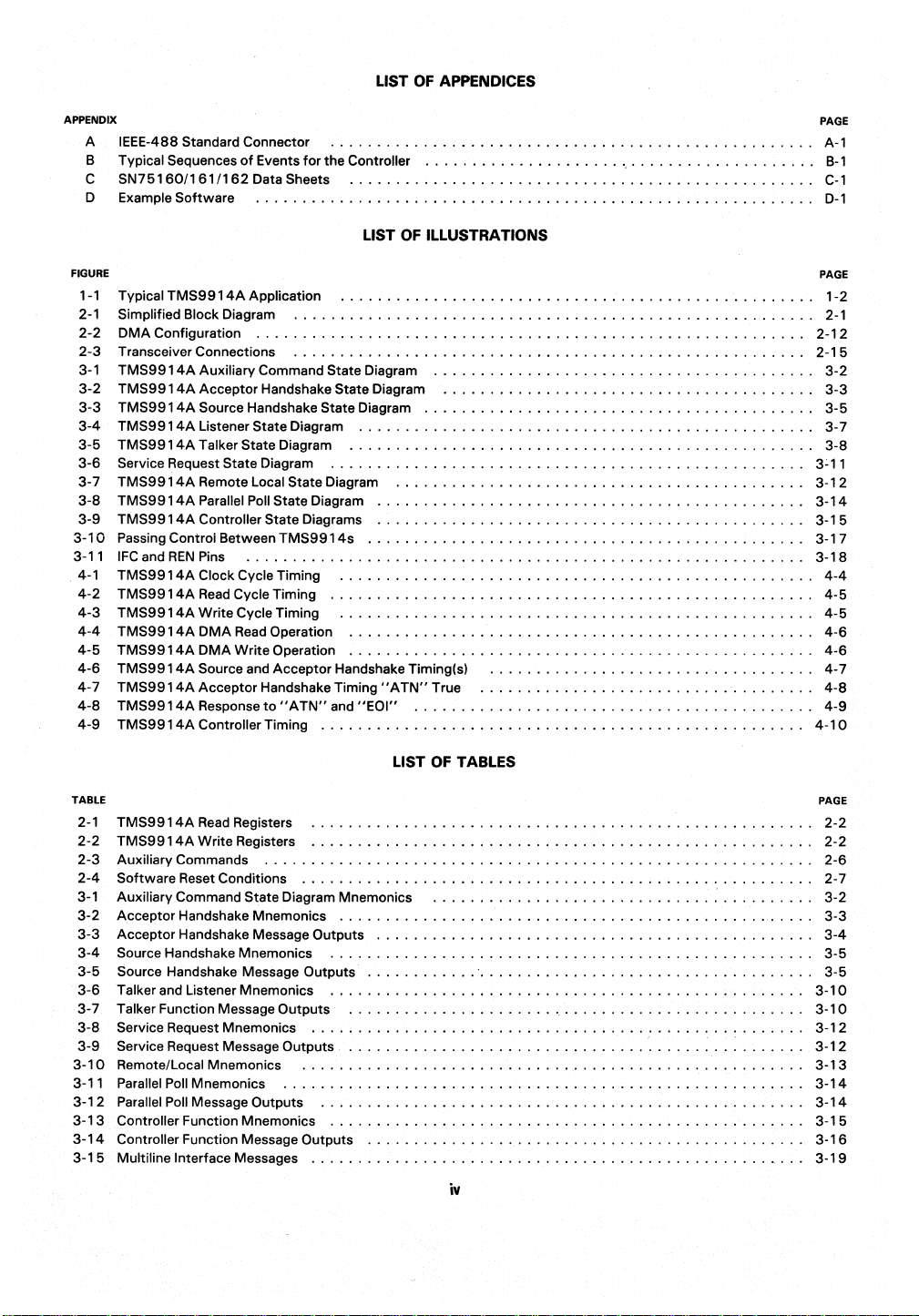
TMS9914A
TMS9914A
3-5
3-6
Service Request State Diagram
3-7
TMS9914A
3-8
TMS9914A
3-9
TMS9914A
3-10
Passing Control Between
3-11
IFC
TMS9914A
4-1
4-2
TMS9914A
TMS9914A
4-3
TMS9914A
4-4
4-5
TMS9914A
TMS9914A
4-6
4-7
TMS9914A
TMS9914A
4-8
4-9
TMS9914A
Software
TMS9914A
Configuration
Auxiliary Command State Diagram
Acceptor
Source Handshake State Diagram
Listener State Diagram
Talker State Diagram
Remote Local State Diagram
Parallel Poll State Diagram
Controller State Diagrams
and
REN
Pins
Clock Cycle Timing
Read
Write
DMA
DMA
Source and
Acceptor
Response
Controller Timing
Cycle Timing
of
Events
for
the
Data Sheets
Controller
..................................................
..........................................
LIST OF ILLUSTRATIONS
Application
...........................................................
Handshake State Diagram
TMS9914s
............................................................
Cycle Timing
Read
Operation
Write
Operation
Acceptor
Handshake
to
"ATN"
...................................................
........................................................
.......................................................
.........................................
........................................
..........................................
.................................................
..................................................
...................................................
............................................
..............................................
..............................................
...............................................
...................................................
....................................................
...................................................
..................................................
..................................................
Handshake Timing(s)
Timing"
and
....................................................
"EOI"
ATN"
True
...........................................
...................................
....................................
PAGE
A-l
B-1
C-l
0-1
PAGE
1-2
2-1
2-12
2-15
3-2
3-3
3-5
3-7
3-8
3-11
3-12
3-14
3-15
3-17
3-1 8
4-4
4-5
4-5
4-6
4-6
4-7
4-8
4-9
4-10
TABLE
2-1
TMS9914A
2-2
TMS9914A
2-3
Auxiliary Commands
2-4
Software
3-1 Auxiliary Command State Diagram Mnemonics
Acceptor
3-2
Acceptor Handshake Message Outputs
3-3
Source Handshake Mnemonics
3-4
3-5
Source Handshake Message Outputs
3-6
Talker and Listener Mnemonics
3-7
Talker Function Message
3-8
Service Request Mnemonics
3-9
Service Request Message Outputs
3-10
Remote/Local Mnemonics
Parallel Poll Mnemonics
3-11
3-12
Parallel Poll Message Outputs
3-13
Controller Function Mnemonics
3-14
Controller Function Message Outputs
3-1 5
Multiline Interface Messages
Read
Registers
Write
Registers
...........................................................
Reset Conditions
Handshake Mnemonics
.......................................................
Outputs
.....................................................
.....................................................
...................................................
...............................................
....................................................
................................................
...................................................
.................................................
.................................................
...................................................
...............................................
LIST
OF
TABLES
.........................................
iv
PAGE
2-2
2-2
2-6
2-7
3-2
3-3
3-4
3-5
3-5
3-10
3-10
3-12
3-1 2
3-13
3-14
3-14
3-15
3-1 6
3·1 9

1. INTRODUCTION
1.1
1.2
1.3
DESCRIPTION
The
TMS9914A
(GPIB)
specified in the IEEE·488
ed
and configured through
plemented, including
KEY
FEATURES
• Handles a" IEEE-488
• Compatible
• Talker and listener function (T,TE,L,LE)
• Automatic source and acceptor handshakes (SH,AH)
• Controller
• System Controller capabilities
• Device trigger and device clear capabilities (DT,DC)
• Optional
• Para"el and serial po" facilities
• Remotellocal function
• Single or dual primary addressing
• Secondary address capabilities
• Direct interface
• Compatible
• Direct memory access facilities
• Memory-mapped microprocessor interface
RELATIONSHIP TO
The
TMS9914A
tions. New features are included on the
disabled
at
provides
with
with
automatically cleared 'request service
with
THE
is compatible
power-up and must
an
interface between a Microprocessor System and the General Purpose Interface Bus
1975/78
8-bit
talker, listener and controller.
1975/78
IEEE-488A
pass control
with
local lockout
to
SN7
5160/161/162
most microprocessors
TMS9914
with
be
standards and the IEEE-488A
memory mapped registers and enables a" aspects
functions
1980
supplement
bit'
(PP)
the
programmed by the user
(RL)
bus transceivers
TMS9914
TMS9914A
with
and may replace
which increase the flexibility
as
needed.
1980
supplement. The device is contro"-
no additional logic
it
in any application
of
the device. These features are
of
the standards
without
to
be
im-
software altera-
TMS9914A
1) Byte Output interrupt modification
2) Reduced bus settling time
3) Modification
4) Addition
VS.
TMS9914:
(see
Section 2.1.1
T1
(see
Section
2.1.6
to
the Service Request Function
of
a second request service (rsv) bit which is automatically cleared
(see
3.5)
1.4
INTRODUCTION TO
The
GPIB
is designed
common bus.
formation is transmitted in byte serial bit para"el format and may consist
face messages, commonly referred
Device data may
structions, such
this way.
One
of
the devices
messages. Devices can
and may
The bus itself consists
grounds. A diagram showing the
be
THE
IEEE-488
to
allow up to 1 5 instruments within a localized
Each
device has a unique address, read from external switches at power-on,
be
sent by
as
select range, select function, or measurement data
on
the bus, designated the Controller in charge (Contro"er), may send interface control
be
assigned
switched between remote and local control.
of
a 24-wire shielded cable. Eight lines carry data; 8
anyone
IEEE
1975/78
to
device (the talker) and received by a number
to
INTERFACE
as
data or commands, respectively.
the bus
as
listeners or talkers by sending their unique talk or listen addresses
bus configuration is given
1-1
and
Appendix
and Section
Section 3.5)
BUS
in
B)
3.3)
(see
Section
area
to communicate
of
either device-dependent data or inter-
for
processing or printout, may
are
control lines; 8
Appendix-A.
with
to
which
of
other devices (listeners). In-
are
2.1.6
and Section
each other over a
it
responds. In-
be
sent in
signal
and
system

Three
of
the management lines operate
as
new data is sent until each device addressed
·method
of
asynchronous communication ensures
as
ensuring compatibility over a wide range
of
The remainder
this manual assumes working familiarity
abbreviations defined within these standards
local messages and upper case
for
remote messages (received via the interface) is used in all acronyms.
a three-line handshake between talker (or controller) and listeners. No
to
listen has received the last byte and is ready
that
the data rate is suited
of
devices.
with
the IEEE-488
are
freely used throughout. The
to
the slowest active listener,
1975/78
IEEE
standards. Terminology and
convention
for
the next. This
of
lower case for
as
well
1.5
TYPICAL APPLICATIONS
The
TMS9914A
pose Interface Bus
processor
does
not
of
have
is used when
(GPIB).
the task
of
to
be
continually polled, and
an
intelligent instrument is required
It
performs the interface function between the microprocessor and bus and relieves the
maintaining the
IEEE
fast
protocol.
responses
By
ed.
A block diagram showing the
The
GPIB
input/output pins
controlled by the
pendix
C)
TE
and
are
designed specifically
devices so that the buffers on particular
used,
but
they may require a small amount
Communication between the microprocessor and
are
13
registers within the
and
get
status information from the device.
The three
least significant address lines from the
TMS9914A
are
connected
Cc.5N'f
outputs generated on the
for
use
lines are controlled
TMS9914A, 6 of
in a typical application is given in Figure 1-1.
to
the
IEEE,-488
with a GPIB
interface. The
ofaxternallogic,
TMS9914A
which are read and 7 write. These registers both pass control data
MPU
are connected
and determine the particular register selected. The high order address lines
CE
input
to
the
the
TMS9914A
the internal registers appear
writing
to
these locations transfers information between the
and writing to the same location
to be pulled
to
be
will
low
when
anyone
situated
at
eight consecutive locations
not
access the same register within the
only or write-only registers. For example, a read operation
GPIB
interface control lines, whereas a write
Each
device on the bus interface is given a 5-bit address enabling
.dress is set on
an
external
DIP
switch (usually
to
this location loads the auxiliary command register.
at
the rear
to
communicate
utilizing the interrupt capabilities
to
changes in
the
with
an
IEEE-488 General Pur-
of
the device, the bus
interface configuration can be achiev-
bus via bus transceivers. The direction
TMS9914A.
as
The
SN75160,
TE
and CONT signals are routed within the
required by the
75161
TMS9914A.
and
75162
Other buffers may be
particularly around the EOlline buffer.
is carried out via memory-mapped registers. There
to
the register select lines
are
decoded by external logic
of
eight consecutive addresses
within
the
TMS9914A
and the microprocessor. Note that reading
TMS9914A
with
RS2-RSO = 011
it
to
be
addressed
of
an
instrument) before power-on.
MPU
gives the current status
as
RSO,
are
address space. Reading
since they
a talker or listener. This ad-
of
data
flow
(see
Ap-
to
RS
1, and
RS2
to
cause
selected. Thus
or
are
either read-
of
the
is
IEEE-4aa
GPIB
DATA BUFFERS
BUS
75160
t----tTE
FIGURE
ADDRESS
SWITCHES
DATA
BUS
TMS9914A
GPIB
1-1 - TYPICAL
WE
....
-+
DBIN
....
-+-~---I
TMS9914A
1-2
DATA AND
PROGRAM
MEMORV
....
1----1
APPLICA
DBIN
MPU
AO·At.
nON

Typical
TMS9914A
register may consist
read. This allows the host
dress register
My
Address (MAl interrupt and entering the required addressed state when this address is detected
data lines.
configuration utilizes registers
of
of a DIP
the
switch which drives the data lines via tristate buffers when one
MPU
to
read
TMS9914A
for device identification on the bus. The
100
or 101
a device address which
as
an
address switch register (see Table 2-1
is
manually set
and
write this address into the ad-
TMS9914A
rasponds by causing a
of
these addresses
on
the
I.
This
GPIB
is
1-3

2.
ARCHITECTURE
The block diagram
are
1 3 MPU accessible registers
tween the IEEE-488
Each
register is accessed by putting the relevant address on lines
read
(WE
= 1 DBIN = 1 ) or memory write
shown in
given in the
Implementation
IEEE-488 state diagram block. Information is received from the
bined
to
Table 2-1
with
load registers or handle the handshake or bus management lines.
of
the internal architecture
of
1975/78
for
following paragraphs.
the current status
REN, IFC, ATN,
EOI,
NRFD&
the read registers and Table
of
the functions described by the state diagrams
SRO,
DAV,
NDAC.
which 6 are read and 7
bus and microprocessor.
(WE
of
the device (for example, Talker Active State, TACS) to produce the control signals
~J1
1
-RESET
-CLOCK
~
4-INT-
INTERRUPT
TR
LOGIC
~
IEEE-488
STATE
DIAGRAM
&
CONTROL
LOGIC
MULTILINE
MESSAGE
DECODE
of
the
TMS9914A
= 0 DBIN =
2-2
A
K
"
is given in Figure
are
write: These registers handle all communication
RSO,
RS1
0)
operation. The register addresses
for
the write registers. A full description
of
the IEEE-488 standard is carried out in the
IEEE
bus and from the internal registers and is com-
0101·
0108
.01
~
-
2-1.
AND
REGISTER
ADDRESS
DECODE
As previously stated, there
RS2
and performing a memory
and
I---ACCRO
i---ACCGR
use
of
each bit is
of
each register is
RSO-2
DBIN
eE
Wl
be-
INTSTATO
INTMASKO
INTSTAT
INT MASK 1
ADDR STAT
BUS
STAT
r-r--
1
r-r--
-
~
AUXCMD
DECODE
AUXCMD
r'}~7
00-07
~
IEEE-488
L~RE
LOGIC
ADDRESS
~
I
FIGURE
."'>.
I
MICROPROCESSOR
2-1-SIMPLIFIED
L
r-J
I
DATA
BLOCK
2-1
DATA
D
SER
P'LL POLL
DATA
~
BUS
DIAGRAM
POLL
OUT
BUS
I
I-
-
-
0
DATA
CPT
IN
I I
~

TABLE 2-1 -
TMS9914A
READ
REGISTERS
ADDRESS
RS1
RS2
0
0
0
0
1 0 0
1 0 1
1 1 0 Cmd Pass Thru 0108 0107 0106 0105
1
"The
TMS9914A
Register may therefore be included
ADDRESS
RS2
0 0
0
RSO
0
0
0 1
1
0 Address Status
1 1
1
1 Data
host interface data lines will remain in the high impedance state when these register locations
RS1
RSO
0 Int
0 1 Int Mask 1
0 1 0
0 1 1
1 0 0 Address edpa dal dat
0
1
1 1 0
1 1 1 Data Out 0108
"This
address is
2.1
1
not
decoded by the TMS
REGISTERS
REGISTER
NAME
Int
Status 0
Int
Status 1
Bus
Status ATN OAV NOAC
DO
INTO
GET
REM
"
"
In
in
the address space
REGISTER
Mask 0
"
Auxiliary Cmd
Serial
Poll
Parallel Poll
9914A. A write
TABLE
NAME
0108 0107 0106 0105
of
the device
to
at
these locations (see Section
2-2 -TMS9914A
DO
GET
xx
cs
58
PP8 PP7
this location
D1
INTl
ERR
UNC
ATN
LLO
WRITE
D1
ERR
UNC
xx
xx
rsvl S6 S5
PP6
0107 0106
will
have no
effect
BIT ASSIGNMENT
f3
if a write
D5 D6
SPAS
LADS
SRO
0103 0102
0103
are
SPAS
0103 0102
RLC
MA
SRO
TAOS
IFC
0102 0101
addressed. An Address
D5
D6
RLC
SRO
MA
f2
A3
S3
PP3 PP2
had not occurred.
D2
D2 D3
D3
BI
BO
APT
LPAS
NRFO
REGISTERS
BIT ASSIGNMENT
BI
BO
APT OCAS
xx xx xx xx xx
xx
f4
A5
PP5
0105
on the device, as
D4
END
OCAS
TPAS
EOI
0104
0104
1.5).
D4
END
A4
S4
PP4
0104
fl
A2
S2
D7
MAC
IFC
ulpa
REN
0101
Switch
D7
MAC
IFC
xx
fO
AI
SI
PPI
0101
2.1.1
Interrupt Mask and Status Registers 0
The Interrupt Mask and Interrupt Status registers operate independently
be set when the appropriate events occur regardless
All
when the appropriate condition becomes true. The storage bits are cleared immediately
terrupt Status Register is read by the
then the event is stored. The corresponding bit is set when the read operation ends, hence no interrupts are lost.
addition
and the
The interrupt status bits are cleared and held in the
The corresponding
nal
'swrst'
the host MPU before
The INTO and
masked interrupt status bits set
Status Register 0
be pulled
The individual bits
The conditions which set these bits,
Section
interrupt bits,
to
61
interrupt (lNT Low) when
with
the exception
being cleared by a read operation, the
interrupt is cleared by reading
bit
of
the Interrupt Mask register
it
or the Hardware Reset pin
'swrst'
is cleared
INTI
bits
of
the Interrupt Status Register are
to
are
unmasked and set
low
3.
provided
Each
that
the Disable All Interrupts feature (dai) has
of
Interrupt Status and Interrupt Mask Register 0 are described are in the following paragraphs.
bit is set on the rising edge
of
the state
of
INTO and
host
the
INTI
which
MPU. If an interrupt condition becomes true during this read operation,
60
interrupt
Data In Register.
of
are
not
is
also cleared by
0 condition while Software Reset (swrst) is set.
must
be set
to
a 1
is
set (Le.,
(RESET)
INT=INT
and will
to
avoid extraneous interrupts (see Section
STATUS.lNT MASK). The mask register is
power
on in a random state.
not
true status bits.
a 1 in Interrupt Status Register 1 . INTO
to
a 1.
If
either INT1 or INTO is true, then the external interrupt pin (INT)
shown
in parentheses, are given in terms
of
the condition shown.
2-2
of
each other. The status bits
will
always
the corresponding mask bit.
storage bits, are edge triggered and are set
after
the corresponding In·
writing
to
the Data Out Register,
if
an interrupt status bit
It
must, therefore, be
2.1.6
INTI
will
will
be true
not
been set.
of
the state diagrams described in
for operation
be
true
if
any
of
is
to
cause an exter·
not
cleared by
written
of
'swrst').
if
there are any un·
bits 2-7
of
Interrupt
to
In
by
will

INTERRUPT MASK/STATUS REGISTER 0
xx
INTO INT1
DO
NOTE: A 0 masks and a 1 unmasks the bits in the interrupt mask registers.
INT1 This
INTO
BI
This
Byte In. A data
is generated
shake feature is
Register
BO
Byte Out. This is set when the Data
be either a command
becomes
byte
TMS9914A
reading
(Set On: SGNS.CACS+ SGNS.TACS.SHFS)
xx
01
will
be a 1 when an unmasked status
will
be a 1 when any
as
an
which has
Interrupt Status Register
When a controller addresses itself
momentary transition
it
reenters SGNS. Under these circumstances, the
BO
going
immediately after
(see Appendix B
BI
BO
END
SPAS
BI
BO
END
SPAS
02
03
04
05
bit
of
bits
2-7
of
Interrupt Status Register 0
byte
has been received in
but a RFD
holdoff
will still occur before the
used, then this status
well as
after
Interrupt Status Register 0 has been read. (Set On: ACDS1.LACS)
if
the device is a controller or data
active talker or controller
not
been sent. Subsequently,
returns
to
SGNS. This
the
Data In register.
bit
will
Out
Register is available
but
will
bit
is cleared
O.
as
of
the source handshake
interrupt on reentering 'SGNS'. The
to
standby
as
a talker should
writing
the
for
details).
write
gts
auxiliary command,
in Interrupt Status Register 1
not
a talker and then goes
TMS9914,
not
be
occur
it
will occur
by
NOTE
the
first
RLC
MAC
RLC
MAC
06
If
next
data byte is accepted.
set. This
to
send a byte over the
if
the device is a talker.
if
the Data Out register has been loaded
after
writing
into
SIDS before T ACS becomes true and
TMS9914A
INT
INT
07
is
set
is
unmasked and set
the mask bit is
bit
is
not
cleared by reading the Data In
It
each
byte
has been sent and the
to
the Data Out Register
to
standby, there
is guaranteed
MASK
STATUS 0
MPU BUS
to
set, then no interrupt
If
the Shadow Hand-
GPIB.
is set when the device
however, may not, and a controller
byte
of
data
into
the Data Out Register
without
waiting for a
BO
0
a 1.
to
a 1.
This byte may
as
well
will
be a
to
give a
interrupt
with
as
a
by
END
SPAS
This indicates
with
the
This indicates
Auxiliary Command Register) and has been polled in a serial poll.
when
the
RLC
Remote/Local Change. This
Remote/Local function.
(Set On: (LOCS-REMS) + (REMS-LOCS) + (LWLS-RWLS) + (RWLS-LWLS)
MAC
My
Address Change. This indicates
resulted in
being used, nor indicate
(Set On:
2.1.2
Interrupt Mask and Status Registers 1
of
The operation
that
cept
Interrupt Mask and Status Register 1 is similar
all bits
are
'swrst'.
There is one distinct group
commands received over the bus and
It
question is set.
may be released
that
a byte just received by a listener was the last byte in a string,
EOIline true.
that
It
the
TMS9914A
is set
serial poll status byte
the
addressed state
that
at
the
same time
as
the
BI
interrupt. (Set On: (ACDS1.LACS.EOI)
has requested service via rsv1 or rsv2 (in the Serial Poll Register or
It
is set on the false transition
is
sent. (Set On: STRS.SPAS.(APRS1 +APRS2)
is
set
by
any transition between local and remote states in the
that
a command has been received from the
of
the
the
TMS9914A
TMS9914A
to
change. It
will
not
occur
has been readdressed on its other primary address.
that
is,
it
was received
of
GPIB
which has
if
secondary addressing
ACDS1.(MTA.TADSUNT+OTA.TADS+MLA.LADS+UN.LADS)
to
that
of
Interrupt Mask and Status Register 0 ex-
true storage bits. The status bits are cleared only following the register being read and
of
interrupts in this register: GET, UNC, APT, DCAS,
if
unmasked, a Data Accepted (DAC) holdoff will occur when the interrupt in
with a 'dacr'
auxiliary command. This is further discussed in Section
MA.
These are all set in response
3.2.
2-3
STRS
is
by
to

The mask
ed, the
tions
The individual bits
these bits, shown in parentheses, are given in terms
bit
of
the APT interrupt is further used in the talker and listener functions. When the interrupt is unmask-
talker and listener functions
of
IEEE-488. Otherwise these functions implement the talker and listener functions
of
Interrupt Status and Interrupt Mask Register 1 are described below. The conditions which set
of
the
TMS9914A
implement the extended talker and extended listener func-
of
the state diagrams described in Section
of
IEEE-488.
3.
INTERRUPT MASK/STATUS
APT~
03 03
GET
GET
GET
This is set
DO
ERR
ERR
01
if
masked. The
holdoff
DAC
UNC
UNC APT OCAS
a Group Execute Trigger command
TR
pin becomes high when this command is received and persists high
if
one occurs. If the interrupt is masked, the
clock cycles.
(Set On: GET.LADS.ACDSH
ERR
Error. This
is
set
if
the source handshake becomes active and finds
both high. This indicates that,
(Set On:
SERS)
UNC Unrecognized Command. This
TMS9914A.
cept
for
'pts'
which
spected in the Command
(Set On:
APT Address
Unrecognized addressed commands will only cause this interrupt
TCT which will only interrupt in TAOS. Secondary commands will only cause this interrupt
auxiliary command has been set previously. A DAC
effectively enables the command pass through feature. Unrecognized commands may be in-
Pass
ACDS1.(UCG.LLO.SPE.SPD.DCL+ACG.GET.GTL.SDC.TCT.LADS+TCT.TADS+SCG.pts))
Pass
Through. Unmasking this interrupt enables secondary addressing. It
command is received provided
of
the
dress
Command
'cs'
bit
of
TMS9914A.
Pass
Through Register. The hold
the Auxiliary Command Register
A DAC holdoff will occur and the secondary address may
secondary has been .identified
(Set On: ACDS1.SCG.(LPAS
DCAS
Device Clear
Active
State. This
selected device clear (SOC) is received
unmasked.
(Set
On:
ACDS1.(DCL+SDC.LADS))
SRQ Service
Request. This is provided
response
to
this interrupt.
It
(Set On: SRQ.(CIDS + CADSH
MA
IFC
My
Address. This is set when the
holdoff
will
occur
if
this is unmasked.
(Set On:
(MLA+MTA).SPMS.aptmkH
Interface Clear. This is provided
IFC
when the
line becomes true and indicates
the device is the System Controller, then the
(Set On: IFCIN)
OCAS
04
REGISTER
MA
MA
05
is
1
SRO IFC INT
SRO IFC INT STATUS 1
06
received. A DAC
07
holdoff
MASK
MPU BUS
occurs
1
if
the interrupt
for
TR
pin becomes high
that
for
whatever reason, there are no acceptors on the bus.
is
set
if
a command has been received which has no meaning
holdoff
will occur
Through Register before this
that
the last primary command received was a primary talk
holdoff
is
released.
for
approximately five
the NDAC and NRFD lines are
if
the device is LADS ex-
if
this interrupt is unmasked
is
set
be
off
by
the host MPU.
may be released
is
used
to
indicate
by
a 'dacr' auxiliary command and the
that a "alid
(cs = 1) or an invalid (cs = 0)
+ TPAS))
is
set when a device clear comm8l1d (DCL) is received or when a
with
the
for
the benefit
is set when the
TMS9914A
for
the benefit
TMS9914A
of
the controller which should execute a serial poll in
SRQ
line becomes true.
recognizes its primary talk or listen address. A DAC
of
devices which are
that
the
IFC
interrupt is
in LADS. This will cause a DAC
not
the System Controller.
TMS9914A
has been returned
not
set.
to
is
the duration
to
if
a secondary
or
listen ad-
read from the
holdoff
It
an idle state. If
un-
of
the
if
the
is set
a
if
2-4

2.1.3
Addre
REM
..
Status Register
LLO
ATN
LPAS
TPAS
LADS
TAOS
ulpe
DO
REM
LLO
ATN The attention
LPAS
TPAS
LADS(or
TADS(or TACS) The device is addressed
ulpa
2.1.4
Address Register
edpe
DO
edpa Enable
dal Disable listener function
dat Disable talker function
A5-A1 Primary address
Bits
1975/78
or
if
primary address
1.5).
The'
ignored by the address comparator giving
the
The Address Register is not cleared by
01
LACS) The device is addressed
del
01
A5-A 1 of
does not allow a device
set by the host MPU, the
edpa' bit is used
TMS9914A
02 03
The device is in the remote state
Local lockout is in operation
TMS9914A
TMS9914A
This bit shows the
det
02 03
dual primary addressing mode
this register contain the primary address
of
the device into these bits. Often this will
to
was selected is indicated by the 'ulpa' bit
04 05
line is
low
(true) on the bus
is in the listener primary addressed state
is the talker primary addressed state
to
listen
to
talk
LSB
of
the last address recognized by the
A5
of
enable the dual addressing mode
A4
04
the
TMS9914A
to
be
assigned the value
TMS9914A
'swrst'
A3
05 06
is held in
two
consecutive primary addresses
06
A2
of
an
or hardware reset.
07
MPU
BUS
TMS9914A.
A1
07
the device (denoted
11111
for bits
idle state. During this time the host MPU may load the
be
read
from an Address Switch Register
of
the
TMS9914A.
of
the Address Status Register.
A5-A
It
AAAAA
1. When
causes the
for
in Table
'swrst'
the device. The address by which
LSB
3-15).
is true
of
the address
IEEE-488
at
power-up
(see
Section
to
be
2.1.5
Auxiliary Command Register Isee Section
cs
DO
f4-fO Auxiliary command select (see Table 2-3)
cs Clear or set the feature (where applicable)
Auxiliary commands
many
propriate value in bits f4-fO. These values are given in Table 2-3.
The
if
'cs' = '1'
auxiliary commands initiate
bit is unused
All the clear/set auxiliary commands are cleared by the hardware
RESET.
xx xx
01
of
the actions
'cs'
bit is used in most cases when the feature selected by f4-fO is
02
are
and disabled
and
ignored by these commands.
F4
03 04 05 06
used
to
enable end disable most
of
the device. The desired feature is selected by writing a byte
if
• cs' =
an
action
3.1
for
F3
'0'.
of
F2
The holdoff on all data (hdfa) feature is an example
the
TMS9914A,
Auxiliary Command State Diagram)
F1
FO
07
of
the selectable features
of
the clear/set type. The feature is enabled
such
as
release
RFD
RESET
pin except
of
the
holdoff (rhdf). In most cases, the
2·5
TMS9914A
to
this register
of
such a feature. Other
'swrst:
which is set true by
and
with
to
the
initiate
ap-
'cs'

The force group execute trigger (fget) and return
and a pulsed mode
of
operation. They behave
to
local (rtll auxiliary commands have a clear/set mode
as
normal clear/set features, but
when they have not been previously set, then they will pulse true. Using the
duce a pulse
a return
remote state next time the listen address occurs
of
approximately 1 ,.s at the
to
one
of
the local states (assuming local lockout is not
TR
TABLE
pin (with a 5 MHz clock). The
(see
Section 3.6).
2-3-AUXILIARY
COMMANDS
in
force) but the
if
they
are
'fget'
command
'rtl'
command used in this
TMS9914A
of
operation
written
with
'cs' = '0'
in
this manner will pro-
way
will cause
may reenter the
cIs
0/1 0 0 0
0/1 0 0 0
na
f4
0 0 0
0/1 0
0/1 0 0
na 0 0 1
0/1 0 0 1
0/1 0 0
na 0 1 0
0/1 0 1 0
011
na 0
na 0 1
na
0/1
011
0/1 1 0 0
na 1 0 0
na 1 0 0
0/1
na
0/1
0/1 1
0/1 1 0 1
0/1
2.1.6
Description
0
0
0 1 1
0 1
1 0 0
1 0
1
1 1
of
Auxiliary Commands
SoftwBre Reset (swrstJ
Setting this command causes the
in any activity on the
while
'swrst'
is set. Configuration should include writing the address
writing mask values into the Interrupt Mask Registers and selecting the desired features
Register and Address Register.
tent
on the
GPIB.
necessary
if
there is no status
various states and other conditions forced by
f3 f2
f1
0
fO
0
MNEMONIC
swrst
0 1 dacr
1
0
0
1
1
0 0 hdfe
0 rhdf
1
hdfa
0 1 nbaf
1
1 0
1 1
1
1
1
0
0
1
0
0 1
0
1
1
1
1 1 gt5
0
0
1
1
0
0
0
1
0
1
0
fget
rtl
feoi
Ion
ton
tca
tcs
rpp
sic
sre
0 1 rqc
1 0
1
1
0
0
1
1
0 0
0 1 stdl
1 0 shdw
1
1 1
0
0/1
xxOOOOO
GPIB.
This auxiliary command is set by the power-on
0
TMS9914A
to
0
be
returned
ric
dai
pts
vstdl
rsv2
to
a known idle state during which
RESET
of
After
this,
'swrst'
may
be
cleared at which point the device becomes logically exis-
The Serial Poll Register and Parallel Poll Registers may also
to
report
as
both
of
these are cleared by the power-on
'swrst'.
FEATURES
Software reset
Release
DAe
holdoff
Release
RFD
hold
off
Holdoff
on
all
data
Holdoff
on
EOI
only
New byte available false
Force group execute trigger
Return
to
local
EOI
with
only
standby
parallel poll
all interrupts
TI
settling time
T1
next byte
delay
it
will not take part
be
configured
Send
Listen
Talk only
Go
to
control asynchronously
Take
control synchronously
Take
Request
interface clear
Send
Send
remote enable
Request control
Release control
Disable
Pass
through next secondary
Short
Shadow handshake
Very short
Request Service Bit 2
and the chip should
the device into the Address Register,
in
the Auxiliary Command
be
written in this period but this is
RESET
pin. Table
2-4
not
lists the
2·6
TABLE
2-4-S0FTWARE
RESET
CONDITIONS
MNEMONIC
SIDS
AIDS Acceptor idle state
TIDS Talker idle state
TPAS
LIDS Listener idle state
LPAS Listener primary state
NPRS
LOCS
CIDS
SPIS
PPSS
ADHS DAC holdoff state
AEHS
SHFS
ENIS
NOTES: 1.
Release DAC
The Data Accepted (DAC)
See
Section 3 for definition
2. All interrupt status bits are held
Holdoff
(dacr)0/1xx00001
holdoff
allows time
secondary addresses, and device trigger
of
above.
in
a 0 state, but interrupt mask bits are not affected.
for
the host microprocessor
or
device clear commands. The
Source idle state
Talker
Negative poll response state
Local state
Controller idle state
Serial poll idle state
Parallel poll standby state
RFD
Source holdoff state
EN
D idle state
quired action has been taken. Normally the command is loaded
with
the address pass through feature
APT interrupt in Section
Release
RFD
Holdoff
Any
Ready For Data
Holdoff
on
All
Data (hdfa)
A Ready For Data
handshake must
Holdoff
on End (hdfe)0/1 xxOO 1
A
RFD
holdoff
will occur when
face. This
Set
holdoff
New
Byte A vailable False (nbaf)naxxOO 101
2.1.2).
(rhdf)naxxOOO
(RFD)
holdoff
0/1
(RFD)
holdoff
be
completed
must be released using
If a talker is interrupted before the
normally be transmitted
as
soon
CS
is set
to
one
if
the secondary address
10
caused by a
'hdfa'
or
'hdfe'
xxOOO 11
is caused on every data byte until the command is loaded
after
each
byte
has been received by the MPU using the
00
an
end
of
data string message
(EOI
'rhdf'.
byte
just
stored in the data
as
the ATN line returns
out
to
the false state. If,
no longer required, its transmission may be suppressed using the
Force Group Execute Trigger (fget)0/1 xxOO
The state
the
is sent
of
the
TR
output
from
the
line is pulsed high for approximately 5 clock cycles
with
CS
equal
to
zero. No interrupts or handshakes are initiated.
110
TMS9914A
is
affected when this command
(1
1'5
at
5 MHz).
Return to Local (rt/J0/1 xxOO 111
Provided
generated (if
bit
CS is set
Force End
This command causes the
is set
the
local lockout (LLO) has
enabled)
to
one the
to
zero, the device may return
or
Identify (feoi) naxxO 1
to
'rtl'
command
inform the
EOI
not
been enabled, the remote/local status
host
microprocessor
must
be cleared (CS = 0) before the device is able
to
remote
that
without
it
should respond
first
000
message
to
be sent
with
the
next
DESCRIPTION
primary idle state
hold
off
on end state
to
with
the clear/set
respond
holdoff
to
unrecognized commands,
is released by the MPU when the re-
bit
at
zero; however, when used
was
valid or
to
zero
if
is released.
with
CS
set
'rhdf'
command.
true
with
ATN false) is received over the inter-
register is sent over the interface, this byte
as
a result
of
the interrupt, this
'nbaf'
command.
is
If
CS
is one, the
clearing'
rtl'.
data byte. The
to
executed.
bit
the
front
to
EOI
If
the CS
TR
line goes high until
is reset, and an interrupt is
panel controls.
return
to
remote control.
line is then reset.
invalid (see
to
zero. The
will
byte
bit
is zero,
'fget'
If
the
is
CS
If
2-7

Listen Only (Ion) 011xx01001
The listener state is activated until the command is sent
Talk
Only (ton) 011xx01010
The talker state is activated until the command is sent
with
with
CS
CS
set
to
0 or until deactivated by a bus command.
set
to
0 or until deactivated by a bus command.
NOTE
'ton'
and 'Ion' are included for use in systems
TMS9914A
itself up
functions are reset
Go
to Standby (gts)naxxO
Issued by the controller in charge
Take
Control Synchronously (tcs)naxxO
Control is again taken by the controller in charge, and ATN is asserted.
shadow handshake command must be used
with
the talkerllisteners and only sends ATN true
rupted.
Request Parallel Poll
This is executed by the controller
must
be
in
the
Command
Take Control Asynchronously
This command is used by the controller in charge
The command is executed
transferring a data byte.
Send Interface Clear
The
troller
troller
Send Remote Enable
Issued
is set false by sending 'sre'
Request Control (rqc)naxx
When the TCT command has been recognized via the unidentified command pass through, this command is sent by
the MPU. The
Release Control (ric)naxx
This command is used after TCT has been sent and handshake completed
to
Disable
The
Pass Through
This feature may be used
(PPC)
'pts'
Through Register. This would
Pass
IFC
line is set true when this command is sent
and should
is
put
into the controller active state.
by
the system controller
another device.
All
Interrupts (dai)011
iNi'
line is disabled,
is passed through the
command is loaded, and the next byte received by the
is being used
as
a listener
Controller Active State
Through Register
be
TMS9914A
Next
Secondary (pts)naxx
or
talker, respectively. Care must therefore
if
sending UNL or OTA.
1011
(rpp)011 xxO
(sic)011 xxO
reset
(sre)011
but
1110
(tca)naxxO
immediately and data corruption or loss may occur
1111
(CS
= 0) after the
xx
10000
to
set the
with
CS
10001
waits
for
10010
xx
10011
the interrupt registers and any holdoffs selected
to
carry out a remote configuration
TMS9914A
be
the parallel poll enable
as
a controller,
to
set the ATN line false.
1101
to
monitor the handshake lines so that the TMS9
in
charge
to
so
that the Attention line is asserted). The poll is completed by reading the
to
obtain the status bits, then sending
1100
IEEE
REN
line true and send the remote enable message over the interface,
at
zero.
the ATN line
10100
as
an
unrecognized addressed command and is identified by the MPU. The
without
a controller. However, where the
it
utilizes the 'Ion' and
at
the end
of
byte transfer. This ensures
send the parallel poll command over the interface (the
to
set the attention line true and
with
CS
set
to
one. This must only
minimum time for
to
go false and then enters the controller active state (CACS).
of
a parallel poll. The parallel poll configure command
TMS9914A
(PPE),
which is read
'ton'
functions
be
taken
to
If
the controller is
'rpp'
with
if
a talker/listener is in the process
IFC
has elapsed (1001'8). The system con-
to
release the ATN line and pass control
are
not affected.
is passed through via the Command
by
the microprocessor.
to
set
ensure these
not
a true listener, the
91
4A
that
no data is lost or cor-
the
CS
bit
at
to
gain control
be
sent by the system con-
is synchronous
zero.
of
TMS9914A
the interface.
of
REN
Pass
2·8

Set
T1
Delay
(std1)1xx10101
The
Tl
delay time can
TI delay time is
to
zero.
Shadow Handshake
This feature enables the controller in charge
transfer. The Data Accepted
ed, and
Not
Ready For Data
The shadow handshake function
so
(ANRS)
also
Very
If
this feature is enabled, the
that
be
received and causes a
Short
Tl
be
set
to
6 clock cycles
11
clock cycles
(2.2
p'S
(shdw)011xx10110
line (DAC) is pulled true a maximum
(NRFD)
is allowed
allows the
A TN can be re-asserted
RFD
hold
Delay
(vstdl
)0/1
xxl
0111
GPIB
settling time
(1.2
P.s
at
5 MHz)
if
this command
at
5 MHz) following a power-on reset or
to
carry
out
the listener handshake
of
to
go false
'tcs'
command
without
causing the loss or corruption
off
to
be generated.
(Tl)
will
be reduced
as
soon
to
be synchronized
cond and subsequent data bytes when ATN is false. Otherwise, the
feature.
Request Service
The rsv2 bit performs the same function as the
vice which
allows minor updates
This
In
addition, rsv2 is cleared when the serial poll status
used in situations where a service request is
As soon
the burden
can occur.
poll
Bit
2 (rsv2)011
is
independent
as
this happens, rsv2 is cleared since
of
clearing the
If
this were
xx
11000
of
the Serial Poll Register.
to
be made
bit
not
from
the host MPU
so, there
to
rsvl
bit
(see Section
the Serial Poll Register
byte
is sent
without
to
simply a request from an instrument
the
reason
for
requesting service has been satisfied. This eliminates
but
also guarantees
would
be a possibility
of
message true, which could result in confusion for the controller. (rsv2
be
noted
that
the
vstdl
It should
and rsv2 features were
not
present on the
is
sent
with
the
CS
bit
at
if
the command is sent
without
participating in a data
with
3 clock cycles after Data Valid (DAV)
as
DAV
is removed.
with
the Acceptor
of
data byte. The
to
3 clock cycles
GPIB
settling time is determined by the
2.1.8)
but provides a means
(600
affecting the state
the
controller during a serial poll. It
for
the controller
that
rsv2
is
cleared before another serial
a second status byte being sent
is
cleared on: SPAS.(APRSl +APRS2).STRS).
TMS9914.
Not
Ready State
END
interrupt can
ns
at
5 MHz) on the
of
requesting ser-
of
the request service.
is
to
poll its status.
with
one. The
CS
set
is
receiv-
se-
stdl
therefore
the
RQS
2.1.7
Bus Status Register
ATN
DO
OAV
01
NOAC
02
The host MPU may examine the status
IFC
bit
of
The
this register does
command.
2.1.8
Serial Poll Register
58
rsvl
0108 0107
DO
01
56 55
0106 0105
02
S8, S6-S0 Device status
rsv 1 Request service
Bits S8, S6-S1
ofthis
cleared by a hardware reset
fully double buffered and
bits are
active state, SPAS), the value
poll
NRFO
03
not
indicate a true value
03
bit
1
register are sent
but
not
by
if
the register is
written
5RQ
EOI
04
S4 S3
0104 0103
04 05
of
the
out
over
'swrst'
05
GPIB
the
and
management lines
0102
GPIB
may
written
REN
IFC
06
S2
06
if
the device
07
51
0101
07
when the device
therefore
be
set up during configuration
to
while the device
MPU
BUS
at
the time
is
a system controller using the
GPIB
MPU
is
addressed during a serial poll. They
.is
addressed during a serial poll (serial
is saved, and these bits are updated when SPAS
2-9
BUS
of
reading.
'sic'
of
the chip. These
is
terminated.
auxiliary
are

The
rsv1
bit provides
quest
that
the controller service the device. When rsv1 is set true, the
controller
typically responds by setting up a serial poll
quire service. When the
with
sent
the
quested a second time. The
The
rev1
bit
is
an
input
to
TMS9914A
RQS
message true on 0107. The rsv1 bit must then
SPAS interrupt is set immediately following the status byte being sent.
also cleared by the hardware reset pin but
quest function comprehends changes in the state
therefore
the rev1 bit
be
written
of
the
to
any time. Section
TMS9914
was
mand.
2.1.9
Command
Pass
Through Register
the service request function
to
obtain the status
is addressed
to
send its status byte,
not
of
rsv1 while the device is in SPAS. The Serial Poll Register may
3.5
contains more information on the service request function. Note
simply referred
to
as
'rsv'
of
the
TMS9914A
SRQ
line is pulled true on the GPIB, and the
of
all instruments on the bus
SRQ
be
cleared and set true again
by
'swrst'.
since
It
is
not
this
device did not have
and is used
to
instruct this
that
to
may
is set false, and the status byte is
if
double-buffered
service is
but
to
be re-
the service re-
that
an
rsv2 auxiliary com-
re-
re-
2.1
0108 0107 0106
DO
01
This provides a means
ed when the data lines are known
parallel poll.
a
It
is used
secondary addresses following
results
of
a parallel poll at least
.10
Parallel Poll Register
PP8 PP7 PP6 PP5 PP4
0108 0107 0106 0105 0104
DO
01
When a controller initiates a parallel poll, the contents
of
the register are cleared, then none
to
the Parallel Poll Idle State
ding
to
the desired parallel poll response is set
Parallel Poll Register is fully double buffered.
The
0105 0104 0103 0102 0101
02
03
of
directly inspecting the
to
read unrecognized commands and secondaries following a UNC interrupt
02
03
04 05 06
to
be
in a steady state such
an
APT interrupt.
2p.s
after setting the
04
GPIB
data lines (010(8-1
In
addition,
'rpp'
PP3 PP2
0103 0102 0101
05 06
of
of
the lines 010(8-1 I will
(PPISI
of
IEEE-488.
to
If
If
it
a 1 .
it
is desired
is
written
07
as
will occur during a OAC holdoff or in CPWS during
an
active controller uses this register
auxiliary command.
PPl
07
this register are presented
be
pulled
to
participate
to
during a parallel poll, the
parallel poll ends, at which point the register is updated. This permits the host
response
If
this register
with
figured
completely asynchronously
is
cleared by the hardware
'swrst'
set.
to
the GPIB.
RESET
pin but not by
'swrst:
GPIB
MPU BUS
II.
It
has no storage and should only be us-
to
GPIB
MPU BUS
to
the
GPIB
data lines.
low
during a parallel poll which corresponds
in
a parallel poll, then the
MPU
it
may
be
loaded while the chip is being con-
new
to
update the parallel poll
bit
value is held until the
or
to
read
read the
If
all bits
correspon-
2.1.11
Data In Register
0108 0107 0106 0105 0104 0103 0102
DO
This register
State (ACOS1) and, following this,
by the host
01
is
used
MPU,
02
to
03 04
hold data received by the
an
but
if the Holdoff
On
05
TMS9914A
RFD
holdoff will occur. This will normally
All Data (hdfal feature
auxiliary command.
2-10
0101
06 07
when
is
selected, this holdoff must
GPIB
MPU BUS
it
is a listener.
It
is loaded during
be
released when the byte is read
be
Accept
released by
the
Data
'rhdf'

If
the Holdoff On
if
the
EOI
line is true
used.
As the Data
In Register
panied by a true
End
(hdfe) feature
when
is
EOI
line.
the
byte
loaded, the
is
selected, theRFD
holdoff
will
be released
is received, reading the data byte will
BI
interrupt is set. The
END
interrupt is set simultaneously
not
release the
by
reading the Data
holdoff
if
the
In
Register. But
and rhdf must
byte
is accom-
be
2.1.12
2.2
Date
Out
Register
0108
The Data
messages. When the
contents
under the control
byte
Handshake becomes active unless a
fect
TMS9914A
0107 0106 0105 0104 0103 0102 0101
DO
of
is sent.
of
clearing
01
Out
the Data
02 03 04 05 06
register is used by a controller or talker
TMS9914A
Out
Register are presented
of
the Source Handshake. Each time a
If
the
handshake is interrupted before the
an
unsent byte from the Data
behaves
as
if it
enters the Talker
new
had
not
been loaded.
byte available false (nbaf) auxiliary command is
to
Out
07
for
sending interface messages and device dependent
Active
State (TACS) or the Controller
the
GPIB
data lines (010(8-1 I), and the
byte
is written, the source handshake is enabled, and the
byte
can
be
sent, then
it
will
Register, and although the register itself
Each time the source handshake becomes active and there is no unsent byte in the Data
will occur informing the host MPU
In
The Data
and its contents
Register and Data Out Register operate independently. The Data Out Register is
are
output
directly
the Data Out Register is available
to
the
data lines
of
the
GPIB.
for
use.
that
DIRECT MEMORY ACCESS
The
TMS9914A
lines. The operation is automatic
ACCRa
The
reset
by
'swrst'
rupt status register
If using
automatically address either the data in register
can operate in
signal is set by (BO.CACS +
readin data in register,
O.
DMA,
the internal
CE
DMA
using the
within
writing
ACCRa
the
TMS9914A
BI)
and can therefore
to
the
data
(DMA request) and ACCGR (DMA grant)
and needs no
not
out
register andACCGR.
'mpu'
configuration.
be used by a controller while ATN
It
is
and addressing is disabled by the ACCGR signal going
(DBIN =
0)
or the data
out
register (DBIN = 1).
GPI8
MPU BUS
Active
byte
be sent
written.
Out
Register, a
not
cleared
State (CACS). the
is sent over the bus
next
time the Source
This has the ef-
is
not
cleared, the
BO
interrupt
not
double buffered,
DMA
handshake
is
asserted.
by
reading inter-
low
and ACCGR will
It
is
2.3
NOTE
At
the end
of a DMA
for
the
'mpu'
to
clear this in some circumstances, e.g., starting
In
DMA
it
is recommended
If
DMA
is
not
being utilized, the ACCGR signal
separate interrupt
line
the interrupt register
The sense
read from memory sequence,
that
for
BO
and
to
find the cause
of
DBIN is inverted
the
MA
interrupt be unmasked
BI.
This allows faster
of
the interrupt. Figure
the
ACCRa
must
be held high. In this case, the
'mpu'
TERMINAL ASSIGNMENTS AND FUNCTIONS
The IEEE-488 standard uses the negative logic convention
a high voltage
TMS9914A
by the device. These terminations are connected
(>
2.0
V); the
are in agreement
TRUE
state (1) is represented by a
with
this convention. For example,
to
the bus via noninverting I:luffers
polarity.
2-11
for
DMA
will
be
DMA
to
prevent errors due
transfers
2-2
for
the
GPIB
low
if
operation.
left
low
(also
BO
bit set).
write
to
memory sequence.
to
ACCRa
to
take place
shows a typical
as
DMA
lines. The FALSE state (0)
voltage
(>
0.8
V). The
Data Valid is true
(1
),
to
It
may be necessary
interrupted data streams.
signal can
it
is
not
be
used
necessary
to
as
read
configuration.
is
represented by
GPIB
the
DAV
terminations
line
is
pulled
ofthe
low
obtain the correct signal
a

Note
that
the terminations on
voltage : false state (0) =
microprocessors. Thus if:
the
microprocessor side
low
voltage). This is in agreement
of
the device are in positive logic (true state (1) = high
with
the logic convention used
by
most
DO(MSB)
o o o o
is written into the data
DI08(MSB)
I
HIGH I lOW I lOW
on the IEEE-488
WE
DBIN
A
MPU
If
~
..
A
out
010
lines.
DMA CONTROL
CE
/'""'~
A
0
0
R
E
S
S
B
U
S
DATA
register,
HIGH
DBIN
I.
,
CONDUCTOR
,.
BUS
it
will appear
lOW
lOGIC
WE
SEMI·
MEMORY
/':..
•
..
-
~~
ADDRESS
DECODE
-
ADDRESS
SWITCHES
ENABLE
HIGH
I
~
as:
ACCRa
ACCGR
WE
DBIN
.,
00·07
.1
v
CE
RS2
D7(lSB)
0101
HIGH
TMS9914A
RS1
(lSB)
lOW
A
/
0101·0108
\
TE
CONi'
A
/
\ MANAGEMENT I
RSO
GPIB
DATA
GPIB
~
\
J
,
..
\
B
U
F
F
V
E
R
1\
S
IEEE
STD488
INTERFACE
BUS
B
U
F
F
~J
E
R
S
A
" 4
"
..
r
r
I
l
FIGURE
2-2-DMA
CONFIGURATION
2-12

TERMINAL ASSIGNMENTS AND FUNCTIONS
SIGNATURE
0108
0107
0106
0105
0104
0103
0102
0101
OAV
NOAC
NRFO
ATN
REN
IFC
SRO
EOI
CONT
TE
DO
01
02
03
04
05
06
07
RSO
RS1
RS2
PIN
31
32
33
34
35
36
37
38
26
24
25
28
22
23
29
27
30
21
17
16
15
14
13
12
11 1I01p/pl
10
6
7
8
I/O
ITYPEI
I/OIP/pl
IIOIP/pl
IIOIP/pl
I/Olp/pl
IIOIP/pl
1I01p/pl
1I01p/pl
IIOIP/pl
IIOIP/pl
1I01p/pl
1I01p/pl
IIOIP/pl
1I0lo/dl
1I01o/dl
IIOIP/pl
IIOIP/pl
Olp/pl
Olp/pl
IIOIP/pl
1I0lp/pl
1I01p/pl
1I01p/pl
IIOIP/pl
1I01p/pl
1I0lp/pl
DESCRIPTION
through
0101
0108
data input/output lines
on the
GPIB
pins connect
488
bus via non-inverting
transceivers.
DATA VALID: handshake line controlled by
source
to
show acceptors when valid data is
present
to
DATA ACCEPTED: handshake line. Ac-
NOT
ceptor sets this false Ihighl when
ched the data from the
NOT
READY
Sent by acceptor
the next byte.
ATTENTION:
When true
being sent over the
Ihighl. these lines carry data.
REMOTE
to
or from the
INTERFACE
troller
known quiescent state. The system controller becomes the controller
SERVICE
device
END
this indicates the end
If
questing a parallel poll.
Indicates
is used
in pass control systems. Logically.
ICIOS+CAOSI.
TALK
transfer
is:ICACS + TACS + EIO.ATN.ICIOS +CAOSI.
'SWRSTI
Data transfer lines on the
of
REGISTER
which register is addressed by the
MPU
ENABLE:
select control either from the front panel
to
set the interface system into a
REOUEST:
to
indicate a need
OR
IDENTIFY:
A TN is true (lowl. the controller is
if
to
control direction
ENABLE:
of
the device
during a read or write operation.
are the
side. These
to
the IEEE-
the bus.
it
has
110
lines.
FOR
DATA: handshake line.
to
indicate readiness for
sent by controller
(lowl. interface commands are
010 lines. When false
sent by system controller
IEEE
bus.
CLEAR: sent by the system con-
set true
if
ATN
of of
a device is controller in charge.
controls the direction of. the
the line transceivers. Logically.
SELECT
LINES: determine
in
charge.
in
charge.
(lowl
by a
for
service.
is
false Ihighl.
a message block.
re-
of
SRO
and A
it
is
MPU
side
lat-
TN
A'CC'Ra
Ac'CGR
CE
WE
081N 0103
RSO
RS1
RS2
iiifi'
07
06
05
04
03
02
01
DO
0
'REsET
VSS
It
it
VCC
TR
0101
0102
0104
0105
0106
0107
0108
COriiT
SRO
ATN
EOI
OAV
NRFD
NDAC
IFe
REN
TE
2·13

TERMINAL ASSIGNMENTS AND FUNCTIONS
(continued)
SIGNATURE
CE
WE
DBIN
INT
ACCRO 1
ACCGR 2 I ACCESS GRANTED: when received from the
RESET"
TR
PIN
3
4 I
5
9
19
39
0 1B I CLOCK input:
VSS
VCC
(pip)
= pus
hi
=
open
All
clear/set
'swrst'
pull output.
drain
auxiliary
(old)
• The hardware
- Serial and Parallel Poll registers cleared
-
-
20
40
output
with
RESET
pin has the following
auxiliary
commands
command
internal pull up .
I/O
(TYPE)
ENABLE:
I
I
O(o/d)
pullup) branch
(no
O(p/p) ACCESS REOUEST: this pin becomes active
I INITIALIZES the
O(p/p)
cleared
set. This holds
CHIP
and
write
in high impedance
WRITE
dicates
written
DATA
dicates
about
INTERRUPT:
to
(low)
direct memory access
enables the byte onto the data bus. ACCGR
must
be
transfer.
TRIGGER:
mand
fget
command
be
synchronous
Ground reference voltage.
Supply voltage
effect
on the
TMS9914A:
except
'swrst'
the
TMS9914A
DESCRIPTION
CE
low
allows access
registers.
ENABLE: when active (low), in-
to
to
BUS
to
the
to
be
to
a service routine.
request a direct memory access.
high when not participating in DMA
activated when the
is
received over the interface or the
in
known
If
CE
is high,
unless
ACCGR
the
TMS9914A
one
of
its
registers.
IN: an active (high) state in-
TMS9914A
carried out by the MPU.
sent
to
the
MPU
control logic this
TMS9914A
is
given by the MPU.
500
kHz
to
5 MHz. Need not
to
system clock.
(+
5 V nominal).
states, as described in Section
00-07
is
that data
that
a read
to
cause a
at power-on.
GET
com-
of
low.
is
is
read
are
being
2.1.6.
2.4
TRANSCEIVER CONNECTIONS
There are three linear transceivers designed
SN7
5162.
Data sheets for these are included
tions. Note
whole
The
of
the
whenever there is
the
which
quired
ed
if
put
The SN7
device or
OAV
input
low
cludes
false (high) and the
that
there is a corresponding pinout between the
GPIB
interface
SN7
5160
buffers is controlled by
is a
20
an
interface
to
be
laid
out
pin device used
the
function
in a very small area
to
Talk Enable
device is in TACS, CACS, SPAS, or PPAS. The Pull-Up Enable
selects
whether
if
faster data rates are required and
the '010(8-1 )' lines are driven by open collector or push/pull buffers. A push/pull
parallel polling is being used in a particular
may
be
hardwired otherwise
5161is a 20-pin
for
a controller
are again controlled by the
of
the
SN7
5161,
which
whenever the
the
TMS9914A
logic necessary
DC
signal
it
must
device used
which
to
does
not
TE
signal. However, the SRO, ATN,
connects
is an active controller,
to
control
the
when
A TN is true (low).
to
work
as
Appendix
buffer
the
IEEE-488 data lines (010(8-1
(TE)
output
of
the
TMS9914A
the'
stdl' and/or
GPIB
environment.
be
derived from ATN and
buffer
the IEEE-488 management lines.
pass control. The direction
to
the Controller
that
direction
of
the
2-14
with
the
TMS9914A:
C.
Figure
2-3
TMS9914A
of
printed circuit board.
of
TMS9914A.
not
sending the NUL message on 010(8-1
(PE)
input
the
'vstdl'
features are used. Open collectors
If
only one
EOI,
as
of
the
REN,
Active
(CONT)
output
is, when
EOI
it
is
not
buffer. This is dependent on
the
shows
the possible transceiver connec-
and the transceivers. This allows the
))
in all applications. The direction
This active high signal becomes true
of
the SN7
of
these 'features is desired
shown
in Figure
It
may be used
handshake line buffers NRFO, NOAC,
and
IFC
buffers are controlled
of
the
TMS9914A.
in CIOS or CADS. The SN7
SN75160,
5160
is
an
2-3.
the
TE
SN75161,
).
that
active high
buffer
must
the
for
a talker/listener
by
CO
NT becomes
5161
signal when
and
is, when
input
is re-
be
us-
PE
in-
the
DC
also inATN
is

The
SN75162
cluding devices which pass control. The
buffers, but is otherwise identical
(SCI which may be hardwired or switchable
or not. Note
troller
'sic'
and 'sre' auxiliary commands
is
a 22-pin device
that
Vee-,-
HIGH
SPEEO
PARALLE
LPOll
G
NO
1
ACCRO
-
ACCGR
-
CE
-
WE
-
OBIN
-
RSO
-
RSI 0105
-
RS2
-
iNi
-
07
-
06
-
05
-
04
-
03
-
02
-
01
-
DO
-
11
-
RESET
-
Vss
-
20
VCC
HIGHSPEEOl
PARALLEL
POL~
GNO _
1
ACciiii
-
ACcGR
-
CE
-
WE
-
OBIN
-
RSO
-
RSI
-
RS2
-
INT
-
07
-
06
-
05
-
04
-
03
-
02
-
01
-
DO
-
0
-
RESET
-
Vss
-
20
which
may be used
to
the SN7
a device which has its buffers configured
for
reasons explained in Section
&...
-
___
TMS9914A
...
1(
----
TMS9914A
1/4
--
J-
vee
TR
0101 0105 0105
lJ
0102
~
0103 0107 0107
0104 0108 0108
0106 1
0107
0106
CONi'
SRa
ATN
EOI
OAV
NRFO
NOAC
IFC
REN
§l,l
TE NDAC
114
SN74LS32
l--
vee
:::
0103
0104
0105
0106 20 •
0107
0108
C~~~
AE~
.:~
TE
'Ef@'
to
buffer the IEEE-488 management lines in all applications in-
SN75162
SN74LS32
~
- J 0103
=--
has a separate pin
51
61 in all other respects. This input
to
determine whether or
as
b
PE
0101 0101
0102
0103 0103
0104 0104
0106 0106
Jill I
~
I~
1111
VCC
DC
SRa
ATN
EOI
OAV
NRFO
IFC
REN
vee
-
20
b SN75160 10
PE
0101
0102
~
::
_m
0107
r 0108
- VCC
b
OC
~
SRa
II~
r-
21
ATN
EOI
OAV
NRFO
NOAC
IFC
REN
NC
-
VCC
-
22
to
control the direction
is
not
the instrument in question is a system con-
a non-system controller should never use the
3.8.3.
SN75160
SN75161
SN75162
GNO
0102
TE
GNO
SRa
ATN
EOI
OAV
NRFO
NOAC
IFC
REN
TE
GNO
0101
0102
0103
0104
0105
0106
0107
0108
GNO
SRa
ATN
EOI
OAV
NRFO
NOAC
IFC
REN
TE
TE
SC
10
-
---
10
r-
~
1
f-
-
1
11
r-
~
1
of
the
REN
and
the System Controller input
IFC
VCc-r
SYSTEM
CONTROLLER
NONoSYSTEM
CONTROLLER
GNO
1
FIGURE
2-3
- TRANSCEIVER CONNECTIONS
2·15

3.
STATE DIAGRAM IMPLEMENTATION
This section presents the state diagrams
Where equivalent, the names
states have been divided,
tion
of
lower
ed.
State diagrams
and F a false output. Parentheses denote a passive output; otherwise,
presented
equivalents.
the
function in question.
No maximum timings
imum timing requirements
other transceivers, then
for
the
of
TMS9914A
for
example, ACDS
case characters
with
to
the bus and assume the use
The symbol (NUL) associated
An
arrow
into
state on the diagram. Note, however,
the destination state are overridden.
an
exit
condition is true then this represents
situations
will
for
local messages and upper case
remote message outputs are supplemented
of
the
with
a state
with
no state
not occur in normal ooeration
are
discussed. The
as
may
it
must
TMS9914A
be
determined
be ensured
that
TMS9914A.
states are the same
of
the IEEE-488 has been split into ACDS1 and ACDS2. The conven-
SN75160
DIO(
1-8)
indicates
NOTE
as
its
origin represents a transition from every other
that
this does
If such
an
entry condition is true and, simultaneously,
an
illegal situation and should
of
with
from
Section
these requirements are still met.
as
those
of
IEEE-488. In some cases, IEEE-488
for
remote messages and interface states is retain-
with
tables. T is used
it
is active. The outputs
and
SN75161
not
the device.
its recommended transceivers meets a1l1EEE-488 max-
4.4
or
SN75162
that
each
of
imply
that
all
and Appendix
to
represent a true
shown
transceivers or their logical
these lines
exit
C.
is
sent passive false by
conditions from
be
avoided. Such
If
the
TMS9914A
are
the values
is used
output
with
3.1
AUXILIARY COMMANDS
There are
cl.ear/set.
The clear/set commands
feature is selected
bit. For the purposes
state.
The immediate execute
mand register has been
to
state diagrams, the immediate execute commands are represented
mand strobe state
The clear/set
ample,
on a secondary address. The 'Ion' and
ed in Section
The
normal
AXSS. In the following state diagrams, however, these are simply included in their clear/set form.
two
basic types
by
the auxiliary command register
bit
of
the auxiliary command register is used by several
'dacr'
uses
it
3.4.
'fget'
and
'rtl'
auxiliary commands are both immediate execute and clear/set. They may be cleared or set in the
way,
but
if
they are cleared when
of
commands implemented in the auxiliary command register: immediate execute and
are
used
the code on fO-f4 (see Section
of
the state diagrams, the mnemonic
auxiliary commands remain active
written
to. This is represented in the
(AXSS)'
to
differentiate between valid and
to
enable and disable the various features
2.1.6)
and
it
is set or cleared according
of
a clear/set command simply represents its current
for
the duration
form
of
must
be spaced
'ton'
they
by
at least five clock cycles. For the purposes
not
valid secondary addresses when releasing a DAC
auxiliary commands
·are
already in the false state,
are
also considered immediate execute,
of
of
a strobe signal after the auxiliary com-
a state diagram in Figure 3-1 . Note
as
the mnemonic gated by the auxiliary com-
of
the immediate execute commands,
they
will
the
TMS9914A.
pulse true
to
the value on
of
for
the duration
The particular
the
cs
that
writes
the remaining
for
ex-
holdoff
as
describ-
of
3-1

FIGURE
TABLE
3·1-TMS9914A
3·1-AUXILIARY
AUXILIARY COMMAND STATE DIAGRAM
COMMAND STATE DIAGRAM MNEMONICS
MESSAGES
3.2
waux
tc(O)
ACCEPTOR HANDSHAKE
The
device remains in
commands which
write to auxiliary
clock
TMS9914A
command
cycle
time
acceptor handshake is shown in Figure
register
AXIS
AXWS
AXSS auxiliary
3·2.
The main variation from IEEE·488
AIDS while the controller function is in CACS. The
it
sends over the bus and this places some restrictions on the user which are outlined in Section
3.8.
The accept data state
In
the Data
Register or
tor'handshake
is used
as
a holding state where the device will remain in the event
As discussed in Section 2.1
(GET,
of
IEEE·488 (ACDS) is divided into
to
sequence the decoding
MA,
MAC, DCAS, APT, UCG,
.2,
certain
of
the commands will cause interrupts in ACDS 1 and,
two
states. The first, (ACDS 1) is used
of
commands from.the bus. All interrupts generated by the accep·
BI,
and
END)
masked, a DAC holdoff will occur. The interrupts concerned are
represented in the state diagram
is unmasked.
It
persists
which inhibits the transition from ACDS2
the
TMS9914A
If a GET
ACDS1 and
to
the various bus commands.
command is received in ACDS1, then the
ACDS2, which means
for
the duration
by
the signal SAHF which becomes true when one
of
ACDS1. This event is stored
to
AWNS. ADHS is cleared
TR
pin will
be
that
if
a DAC holdoff occurs, the
released by a 'dacr' auxiliary command.
Two
additional state diagrams
indicates that a data byte has been received and
are
included
to
record the type
that
an
of
RFD
holdoff should
accepted. The holdoff may be released by reading the Data In Register unless the
case
'rhdf'
must
be
'hdfe'
feature set. This will cause
used. AEHS shows
an
that
the last data byte was accepted
RFD
hold
off
which can only
STATES
auxiliary
auxiliary
TMS9914A,
are generated
of
a DAC holdoff.
GET,
MA,
by
by
'dacr'. Table
command
command
command
therefore, does not monitor the
by
this state. The second (ACDS2)
DCAS, UCG, and APT. This is
of
the above interrupts is set
causing the ADHS
register
writa state
strobe
to
to
if
the interrupts are un·
to
3·15
shows the response
idle
state
state
note is
that
the
strobe data into
if it
become active
of
set high. This high condition persists throughout
TR
pin will remain high until the holdoff is
data received in ACDS1 when ATN is false. ANHS
be
caused before the next data byte
'hdfa'
feature is enabled in which
with
the
EOI
message true and the
be
released by
'rhdf'.
is
3·2

(ATN.CIDS.CADS) 0
swrst +
(ATN.LADS.LACS)
dacr.AXSS
swrst.(ATN.(CIDS+CADS)
+ATN.(LADS+LACS)
~------I~.l
CWAS.DAV.
(ATN+ANHS.AEHS.
rdin.rhdf.AXSS)
DAV
te(O)
swrst
swrst
dacr
rhdf
shdw
rdin
hdfe
hdfa
ATN
OAV
EOI
RFD
DAC
SAHF
tc(O)
swrst.SAH F
.ACDS1
(rhdf.AXSS)+shdw+(rdin.hdfa)
swrst.ATN.ACDS1.shdw
rhdf.AXSS
swrst.ATN.ACDS1.hdfe.EOI
FIGURE
3-2-TMS9914A
TABLE
MESSAGES
software
=
DAC release
=
release
=
shadow handshake
=
read data in register
=
enable
=
ed
enable
=
attention
=
data valid
=
end or identify state
=
ready
=
data accepted
=
set accept data
=
clock
=
RFD
RFD
RFD
for
cycle
reset
hold
holdoff
data
time
holdoff
off
holdoff
after
on all data
state
ACCEPTOR HANDSHAKE STATE DIAGRAM
3-2
- ACCEPTOR HANDSHAKE MNEMONICS
AIDS
ANRS
ACRS
ACDS1
END
messages receiv·
ACDS2
AWNS
ADHS
ANHS
AEHS
CWAS
AXSS
LADS
LACS
CIDS
CADS
ATN.5te(O)+
ATN·te(O)
acceptor idle state
=
acceptor
=
acceptor ready state
=
accept
=
accept
=
acceptor
=
accept
=
acceptor
=
acc;eptor
=
controller
=
(controller function)
auxiliary command strobe state (auxiliary com-
=
mand register)
listener addressed state (listener function)
=
listener active state (listener function)
=
controller idle state (controller function)
=
controller addressed state (controller function)
=
STATES
not
ready state
data state 1
data state 2
wait
for
data
holdoff
not
ready
not
ready
wait
for
new
cycle state
state
holdoff
holdoff
ANRS state
state
after
'END'
3-3
TABLE
3-3-ACCEPTOR
HANDSHAKE MESSAGE OUTPUTS
STATE
ACDSl
ACDS2 F
AWNS
3.3
SOURCE HANDSHAKE
The
REMOTE
AIDS
ANRS F F
ACRS
TMS9914A
MESSAGES SENT
RFD
(T)
(T)
F F
DAC
(T)
F
F
F
(T)
source handshake state diagram is
been removed. These record the
new
data
byte
removed and a
availability
of
a data
byte
is made ready. Instead the
in the Data Out Register. This state is exited when a byte is
Register which enables the transition from SGNS
is reentered as the byte is sent in STRS,
has not been sent is recorded
register is
The status
dent
the Data
The additional state
handshake tries
normally indicate
devices addressed
The state
to
be disregarded, then
byte
in the Serial Poll Register is continually available. The transition
on SHFS during a serial poll,
Out Register, a talker sending data may be interrupted
SERS
to
send a
for
to
VSTS will
be
until the source handshake again becomes active. If, however, the
is included
byte
a controller
listen on the bus.
entered
enables a very short bus settling time (4tc(O))
TMS9914A
will
not
use the short bus settling time when
OTHER
ACTIONS
ATN False: - data entered into Data
BI
interrupt generated
-
- end interrupt generated
ATN true:
TR
shown
false then true transition
to
SDYS and the subsequent transmission
but
if
the handshake is interrupted before this, then the
'nbat'
may be used
-commands
- command related interrupts set
- sahf set
-
-
pin set true
in
Figure
of
'nba'
TMS9914A
to
return the device
if
requires a
TR
message is received
'pts'
after
received
DAC holdoff
pin set true
feature cleared
UNC
if
in
3-3.
IEEE-488 states SIWS and SWNS have
(new
uses a separate state (SHFS)
decoded
command
if
GET
interrupt set
GET
command was
ACDS 1
byte
available)
to
SHFS.
from
that
is, while SPAS is active. By separately recording the availability
for
a serial poll
to
detect
an error condition on the bus. This will be entered when the source
but
finds both the NRFD and NDAC lines false
that
there are no devices powered up on the bus, or
after
the first data
byte
of
a talker has been sent
for
all subsequent bytes until ATN
it
is
an active controller.
without
at
the same time. This condition
if
the
'vstdl'
In
Register
if
EOI
is true.
as
the old data byte is
written
of
the byte. The
byte
SGNS
to
SDYS is not depen-
risk
of a byte
for
a talker
feature
next
becomes true. The
to
to
the Data Out
fact
that
in the data
of
being lost.
that
there are no
is
enabled. This
record the
SHFS
the byte
out
a byte in
will
The
8tc(O)
TMS9914
or
12tc(O)
did
not
for
NOTE
implement the
'stdl'
set and not set respectively.
'VSTS'.
3-4
The bus settling time was therefore either

Iwm.ITACS+SPAS+CAS)
IATN.CACS)+IATN.ITACS+
SPASII+swrst
iWfitwdot
Iwnt
ATliI.vstd1.STRS
ATN.vstd1
FIGURE
3-3-TMS9914A
RFD.DAC.
112tcIO)+std
8tcIO)+VSTS.
4tc10)
SOURCE HANDSHAKE STATE DIAGRAM
MESSAGES STATES
swrst
nbaf
wdot
stdl
vstdl
ATN
RFO
OAC
tc(O)
SIOS
SGNS
SOYS F
SERS
STRS T
software
=
new
=
=
=
=
=
=
=
=
STATE
byte available false
write
to
enable short bus settling time
enable very short bus settling
attention SHFS
ready
data accepted TACS
clock cycle
TABLE
3-4-S0URCE
reset SIOS
the data
out
register
time
for
data VSTS
time
TABLE
3-5
- SOURCE HANDSHAKE MESSAGE OUTPUTS
REMOTE MESSAGES SENT
OAV
(F)
F true
F
HANDSHAKE MNEMONICS
BO
interrupt and
if
SPAS is
ERR
interrupt set true
SGNS
SOYS
SERS
STRS
=
=
=
=
=
=
=
=
CACS
SPAS
AXSS
SHFS is false and
not
=
=
=
OTHER ACTIONS
ACCRa
true
source idle state
source generate state
source delay state
source error state
source transfer state
source hold
very short bus settling
talker active state (talker function)
controller active state (controller function)
serial poll active state (talker function)
auxiliary command strobe state
(auxiliary command register)
set
off
state
time
state
3-5

3.4
TALKER
Figures
listener and talker or extended listener and extended talker functions
APT interrupt mask bit.
The
MPU
cause this interrupt
or LPAS. A OAC hold
the Command
with a 'dacr'
secondary. If a valid secondary address
whether
The 'Ion' and
state diagrams. Therefore, although they appear
cleared by other bus events. For
may
The
only are used in situations where there is no active controller on the bus. Note
linked
of
Second,
for
the talker. Hence, when a controller addresses itself
similarly,
When the
These will remain unchanged until SPAS is exited. The source handshake will, however, send this status byte
many times
The internal
simplify implementation
iliary command is included
system controller
A separate state diagram is included
command is
EOlline will
shake begins
send
to
AND
LISTENER FUNCTIONS
3-4
and
3-5
show
the
TMS9914A
TMS9914A
for
be
returned
'Ion' and
with
IEEE-488.
the 'Ion' and
a controller
EOI
ERAS.
does
not
recognize secondary addresses on-chip and these must be passed through
verification. Secondary addressing is enabled by unmasking the APT interrupt. A secondary address will
if
the last primary command received was a primary address
off
will also occur. The host MPU
Pass
Through Register and identifying
auxiliary command, the sense
it
is in TPAS or LPAS.
'ton'
auxiliary commands together
example,
to
LIDS by an UNL command from the bus
'ton'
auxiliary commands are used
these features
to
if it
sends another talk address over the bus then
TMS9914A
as
the controller
IFC
signal
written
be
asserted
to
send this byte, and
true
with
to
indicate
'ton'
auxiliary commands are used by an active controller
address itself
enters SPAS, the contents
of
to
clear its
followed
the
next
to
listen via
will
accept it.
the
TMS9914A
of
the controller function (see Section
with
IFCIN
own
interface.
to
by
loading a byte into the Data
as
'010(8-1)'
EOI
byte
as
well, then
listener and talker state diagrams, which serve the purpose
of
IEEE-488, depending on the state
of
the device,
must
respond
to
the interrupt by reading
it
as
being valid
of
the'
cs' bit being used
is
indicated then the
with
the clear/set bit (cs) have a direct influence on the appropriate
as
ordinary clear/set auxiliary commands,
if a TMS9914A
to
implement
to
the user
that
these commands are
the'ltn'
and
'Iun'
to
talk via
it
of
the serial poll register
(lFCIN)
is
suppressed when the device itself
to
return the talker and listener functions
control the sending
begin
to
change. The function
will
be
released when the Data
'feoi'
may be
of
Out
written
or
not
valid. The
to
indicate a valid (cs = 1 ) or not valid (cs = 0)
TMS9914A
addresses itself
at
a later time.
two
message but there
'ton:
must un-address itself by
3.8.3).
the
END
Register, the
will enter TAOS
as
features
before the Data Out Register returns the device
of
not
it
must send its talk address over the bus and
are
Therefore, the send interface clear (sic) aux-
message
will
enter ENAS as soon
Out
Register
holdoff
a listener via
IEEE-488. First, talk only and listen
that
the
'Ion'
enabled
by
to
address itself. IEEE-488 provides
is
no corresponding message
sampled and presented on 010(8-1).
to
their idle states and allow a
of
IEEE-488. If the
TMS9914A
is
next loaded.
or
they
and
CAS
writing
is
sending
will
of
of
to
the host
that
is,
it
is
in TPAS
the
secondary from
may then
LADS depending on
the
enter ERAS, and the
be
released
can be effectively
'Ion'
command
'ton'
commands
as
are
'Itn'
and 'Iun'
'ton'
false.
IFC
in
order
'feoi'
auxiliary
as
the source hand-
If
it
is
desired
the
the
it
are
for
as
to
to
3-6
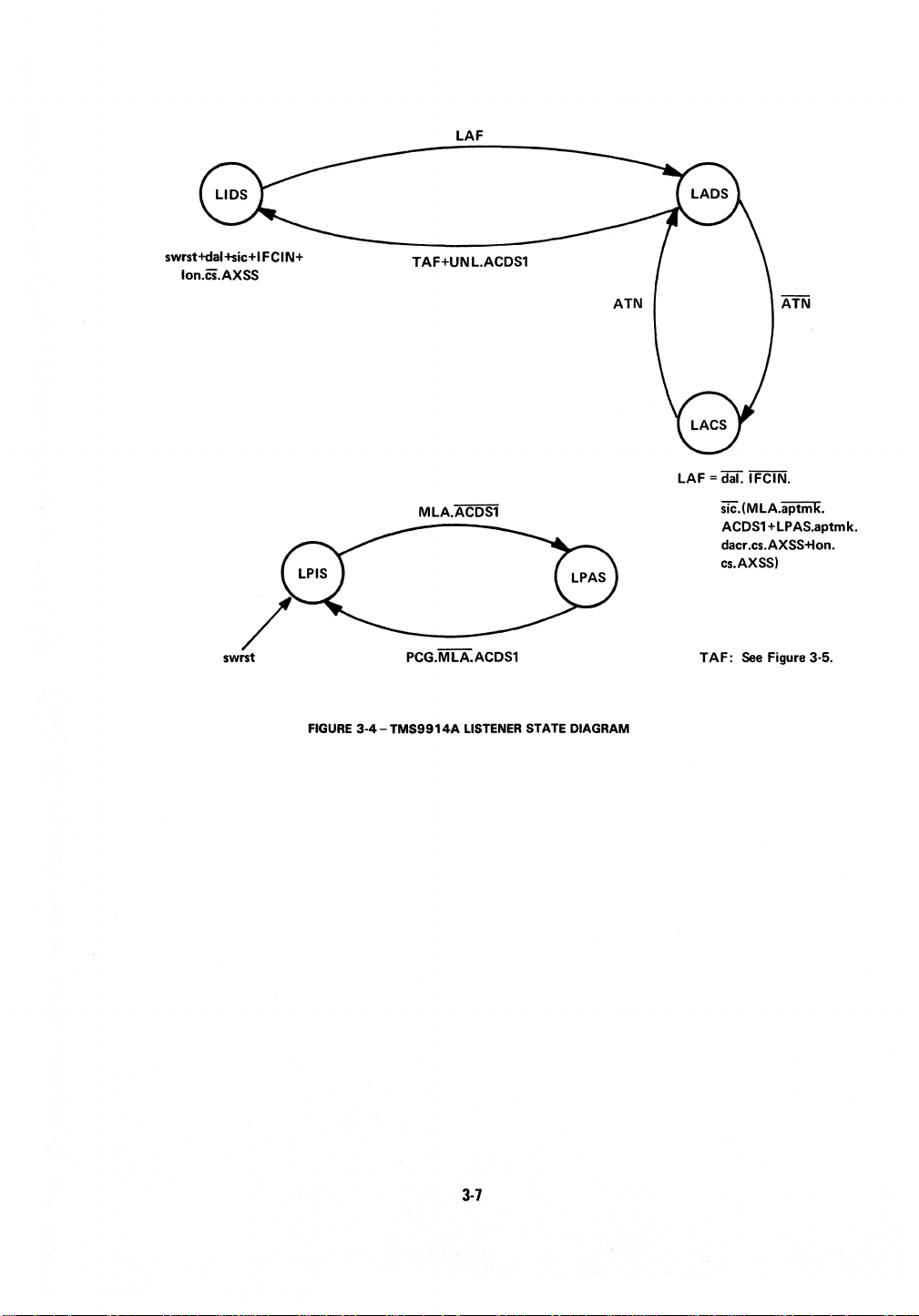
LAF
swrst+dal+Sic+IFCIN+
lon.Cs.AXSS
swrst
FIGURE
TAF+UNL.ACDS1
MLA.ACDS1
PCG.MLA.ACDS1
3·4-TMS9914A
LISTENER
STATE DIAGRAM
LAF = dal. IFCIN.
sic.(MLA.aptmk.
ACDS1
+LPAS.aptmk.
dacr.cs.AXSS+lon.
cs.AXSS)
T AF: See Figure 3·5.
3·7

(TPAS.aptmk.dacr.
cs.AXISS)+LAF+
OTA.ACDS1
TAF
= dat.;lc:i"j:ClN.(MTA.aptmk.ACDS1+
TPAS.aptmk.dacr .cs.AXSS+ton.cs.
AXSS)
LAF:
See
Figure 3-4.
TAF
ATN.SPMS
MTA.ACDS1
PCG.MTA.ACDS1
swrst
iFCiN.SPE.ACDS1
FIGURE
3-5 -TMS9914A
SPD+CIDS+CADS
IFCIN+
swrst
TALKER STATE DIAGRAM
3·8
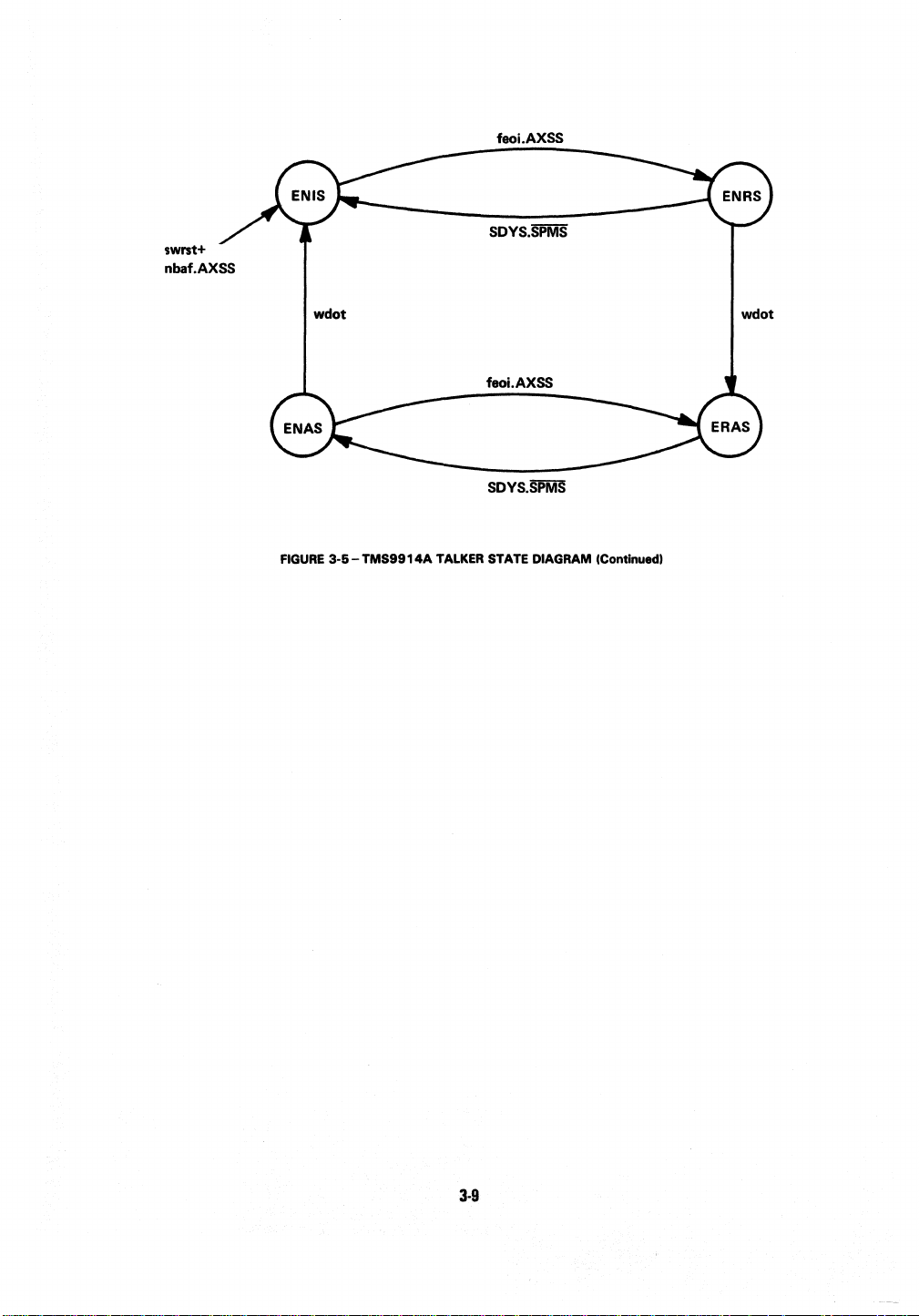
feoi.AXSS
,wrst+
nbaf.AXSS
wdot
FIGURE
3·5-TMS9914A
TALKER
SDYS.SPMS
feoi.AXSS
SDYS.SPMS
STATE
DIAGRAM
wdot
(Continued)
3·9

IAISLI:
;1-6-TALKER
AND
LISTENER MNEMONICS
swrst
dal
dat
sic
Ion
ton
cs
dacr
aptmk
nbaf
feoi
wdot
ATN
IFCIN
EOI
PCG
MLA
MTA
OTA
SPE
SPD
UNL
PCG
software reset
=
disable listener
=
disable talker
=
send interface clear
=
listen only
=
talk only TIDS
=
clear/set bit
=
release
=
address pass through interrupt mask
=
new byte available false
=
force 'EOI'
=
write
=
attention
=
internal interface clear message
=
signal, suppressed by 'sic')
end or identify
-
primary command group
=
my listen address ENAS
=
my talk address
=
other talk address
=
serial poll enable CADS
=
,serial poll disable
=
un listen
=
primary command group
=
MESSAGES STATES
of
the auxiliary command register TADS
'DAC'
hold
off
to
the Data Out Register TPIS
(a
de
bounced
LIDS
lADS
lACS
lPIS
lPAS
TACS
SPAS
SPIS
SPMS
TPAS
ENIS
ENRS
ERAS
SDYS
CIDS
ACDS1
AXSS
listener idle state
=
listener addressed state
=
listener active state
=
listener primary idle state
=
listener primary addressed state
=
talker idle state
=
talker addressed state
=
talker active state
=
serial poll active state
=
serial poll idle state
=
serial poll mode state
=
talker primary idle state
=
talker primary addressed state
=
end idle state
=
end ready state
=
end ready and active state
=
end active state
=
source delay state (source handshake)
=
controller idle state (controller function)
=
controller addressed state (controller function)
=
accept data state 1 (acceptor handshake)
=
auxiliary command strobe state (auxiliary com-
=
mand register)
3.5
STATE
TlOS
TAOS
TACS
TACS
SPAS
SPAS APRS1.APRS2
SERVICE
Figure
plementing
the
REQUEST
3-6
shows
second is
the
the
QUALIFIER RQS
ENIS.ENRS IF)
ENAS.ERAS
NPRS.SRQS
FUNCTION
the state diagram
request service (rsv) local message
auxiliary command
TABLE
3-7-TALKER
for
'rsv2'.
FUNCTION MESSAGE OUTPUTS
REMOTE MESSAGES
(F)
(F)
(F)
F F SERIAL POLL
T
the
TMS9914A
of
IEEE-488:
These are simply
quest function, and, in any particular application, only one
ware reset state.
3-10
SENT
EOI
(F)
(F)
F
T
F SERIAL
OTHER ACTIONS
010(8-1)
(NUL)
(NUL)
DATA
OUT
REG
DATA
OUT
REG
REG
POll
REG
service request function. The device has
the
first,
'rsv1',
is
bit 7 of
the
ORed
would
normally be used,
together
to
provide
an
the
other being
input
two
means
of
im-
Serial Poll Register;
to
the
service re-
left
in
its
hard-
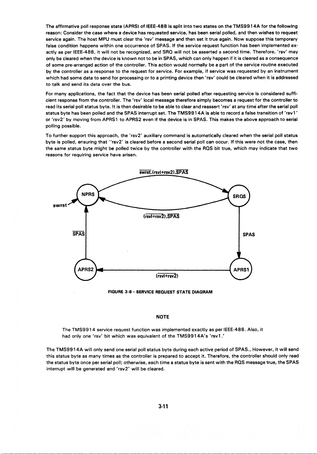
The affirmative poll response state (APRS)
reason: Consider
service again. The
false condition happens
actly as per IEEE-488,
only
be
cleared
of
some pre-arranged action
by the controller as a response
which
had some data
to
talk
and send its data over the bus.
For many applications,
cient response
read
its
serial poll status byte.
status
byte
or
'rsv2'
polling possible.
To further support this approach,
byte
is polled, ensuring
the
same status
reasons
for
swrst
the
case where a device has requested service, has been serial polled, and then wishes
host
MPU
must
clear the
within
one occurrence
it
will
not
be recognized, and SRO will
when
the
device is
to
send
the
from
the controller. The
has been polled and the SPAS interrupt set. The
by moving
from
APRS1
that
byte
might
requiring service have arisen.
known
of
the controller. This action
to
the
request
for
processing or
fact
that
the
'rsv'
It
is then desirable
to
APRS2 even
the
'rsv2'
"rsv2'
is cleared before a second serial poll can occur.
be
polled
twice
of
IEEE-488 is split
'rsv'
message and then set
of
SPAS.
not
to
be
in SPAS,
for
service. For example,
to
a printing device then
device has been serial polled after requesting service is considered
local message therefore simply becomes a request
to
be able
if
the
auxiliary command is automatically cleared
by
the controller
into
two
states on
it
If
the
service request function has been implemented ex-
not
be
asserted a second time. Therefore,
which
can only happen
would
normally be a part
if
'rsv'
to
clear and
TMS9914A
device is in SPAS. This makes
with
reassert'
is able
the
ROS bit true,
the
TMS9914A
true again.
service
Now
if
it
is cleared as a consequence
of
the
was
requested by an instrument
could
be
cleared when
rsv'
at
any
to
record a false transition
the
If
this were
which
suppose
service routine executed
for
time
after
above approach
when
the
not
may indicate
for
the
following
to
this
temporary
'rsv'
it
is
adc;lressed
the
controller
the serial poll
of
to
serial poll
the case, then
that
SWiif.(rsvl+rsv21.SPAS
request
may
suffi-
to
'rsv1'
serial
status
two
FIGURE
The
TMS9914
had only one
The
TMS9914A
this
status
byte
the
status
byte
interrupt will be generated and
service request
'rsv'
bit
will only send one serial poll status
as
many
times as the controller is prepared
once per serial poll; otherwise, each
which
'rsv2'
(rsvl+rsv21.SPAS
3-6-SERVICE
function
was
equivalent
will be cleared.
(rsvl+rsv2)
REQUEST
NOTE
was
implemented
of
byte
time
STATE DIAGRAM
exactly
as per IEEE-488. Also,
the
TMS9914A's
during each active period
to
accept
a status
byte
'rsv1.'
it. Therefore,
is sent
SPAS
of
SPAS., However,
the
controller should only read
with
the ROS message true,
it
it
will
send
the
SPAS
3·11

TABLE
3-B-SERVICE
REQUEST
MNEMONICS
3.6
swrst
srv1
rsv2
STATE
NPRS
SRQS
APRSl
APRS2
REMOTE/LOCAL FUNCTION
The
The complete listener
This means
address,
response
ed
softwerereset
=
request service 1 (bit 7 of seriel
=
request service 2 (auxiliary command register)
=
TMS9914A
that
if
but
if
secondary addressing is enabled,
to
a valid secondary address. In addition,
to
address
the
MESSAGES
TABLE
REMOTE
remote local
function
the
APT
interrupt
device
to
3-9-SERVICE
MESSAGES
SRQ
(F)
T
(F)
(F)
state
diagram is
(LAF) is used
is masked,
listen.
poll
SENT
register)
REQUEST
shown
to
effect
the
device
then
the
the
transition
NPRS
SRQS
APRS1
APRS2
SPAS
MESSAGE
- rsv2 cleared
-
SPAS
interrupt set
-
same
as
in Figure
this
3-7.
transition
will
enter one
will
not
to
STATES
negative
poll
=
service.
=
affirmative
=
affirmative
=
serial poll active state (ta)ker function)
=
OUTPUTS
OTHER
if
in
SPAS
if
APRS
1
It
differs
from
LOCS
of
the
happen until
one
of
the
response
request state
poll
state 1
poll
state 2
ACTIONS
and
STRS
in
SPAS
when
STRS
little
from
that
to
REMS
or
remote states in response
'dacr'
is
written
remote states
state
of
from
will
is
exited
IEEE-488.
LWLS
to
with
'cs'
occur
if
to
RWLS.
its listen
true
'Ion'
in
is us-
swrst+
RENIN---~
RENIN_
LLO
ACDS1
LAF:
See
Figure 3-4
FIGURE
RENIN_rtI.LAF
GTL_LADS.ACDS1+
rtl.( LLO.ACDS1)
GTL.LADS_ACDS
3-7-TMS9914A
LAF
REMOTE
LOCAL
STATE
LLO.
ACDS1
DIAGRAM
3-12

TABLE
3-10
- REMOTE/LOCAL MNEMONICS
swrst
rtl
RENIN
GTL
LLO
3.7
3.7.1
PARALLEL
The parallel poll function
suitable software package, remotely-configured
shown in Figure 3-8.
When the
Register
(PEl
occurring when the Parallel Poll Register is in the hardware reset condition
being pulled low. This corresponds
then the bit corresponding
state
equivalent
Remotely Configured Parallel Poll
The
is passed through when the
then the pass through next secondary (ptsl auxiliary command should
This will cause the next command received
command will
be read from the
(S, P1, P2,
should then
same, the
Poll Register.
this, each time the individual status
the Parallel
If a PPD
cleared before the
means
TMS9914A
Parallel Poll Register before releasing the
software reset
=
return to local
=
internal remote enable message (debounced)
=
go
=
local lockout
=
EOI
are
input
of
(PPSS)' and, when the Identify message becomes true, the appropriate line
to
parallel poll configure command
bit
command is passed through after the
of
eliminating individual members of a parallel poll. The parallel unconfigure command is treated by the
MESSAGES
to
local
POLL
FUNCTION
and ATN lines become true simultaneously (the Identify message), the contents
output
to
the
SN75160
the parallel poll active state (PPASI. Only one bit
be
either the parallel poll enable command
Command
P31
should
be
matched against the individual status
corresponding
If
this is
Poll Register updated accordingly until
OAC
as
an
unrecognized universal command. When
STATES
LOCS
REMS
RWLS
LWLS
LADS
ACDS1
of
the
TMS9914A
010(8-1 I.
be
not
If
parallel poll is
must be held low
to
the parallel poll idle state (PPISI.
to
the desired parallel poll response is set true. This implements the parallel poll standby
(PPCI
TMS9914A
Pass
Through Register and identified.
extracted and stored by the host MPU
to
the parallel poll response, specified by P1, P2, P3, should be set true in the Parallel
the case, then the Parallel Poll Register should be cleared
of
the device changes, the
holdoff is released. The
only nominally supports logically-configured parallel poll.
parallel poll may also
to
be
used in a particular bus environment, then the Pull-Up Enable
so
that
the 010(8-1 I are driven by open collector buffers. Parallel Poll,
of
the parallel Poll Register should be set true
is treated by the
is in LADS.
to
also set a UNC interrupt
'pts'
PPC
OAC
holdoff. This command will clear all members
TMS9914A
If
an
instrument is
(PPEI
or the parallel poll disable command
If
(see
of
the instrument (represented by
'ist'
PPD
or
PPU
is received.
feature
has
been written, the Parallel Poll Register should
command that precedes
it
is passed'through, the host MPU should clear its
local state
=
ramote state
=
remote
with
=
local
=
listener addressed state (listener function)
=
accept data state 1 (acceptor handshake)
=
be
easily implemented. The state diagram is
of
all zeros, will result in none
If
it
is desired
as
an
unrecognized addressed command.
to
be
be
written before releasing the DAC holdoff.
if it
is a secondary command. The secondary
it
is the
PPE
Section
should again
lockout state
with
lockout state
of
to
participate in a parallel poll,
of
010(8-1)
remotely configured for parallel poll,
command, then the attendant bits
2.9.3
of
if it
be
matched against the S bit and
PPO
is
an
is
pulled low. This is
(PPD)
IEEE-488
is
1978).
'ist'l,
and
not
already clear.
address command;
of
a parallel poll.
With
the Parallel Poll
of
010(8-1 I
at
once.
and should
The S
bit
if
they
are
the
After
be
it
is a
a
It
3·13

IWrst
FIGURE
iWrit.ATN.EOI.(CIDS+CADS)
3·8-TMS9914A
TABLE
3·11
PARALLEL
- PARALLEL POLL MNEMONICS
POLL
STATE DIAGRAM
MESSAGES
PPSS
PPAS
CIOS
CADS
POLL
01018·11
(NULl
POLL
REG
is greatly simplified compared
it
enables all subsets
to
a small proportion
supplement
DAV
to
be
an
of
this command until the acceptor handshake enters ANRS and the
microseconds
included on the TMS99 1
•
3.8
swrst
ATN
EOI
STATE
PPSS
PPSS
If
there
Is
a true bit In the Parallel Poll Register.
CONTROLLER
softwara
=
attention
=
end
=
FUNCTION
The controller function
software support but,
With
this approach the controller logic is reduced
may
be
economicelly used in situations where a talker/listener only
Figure
3·9
shows the controller function state diagram. With suitable software,
function,
as
described in the IEEE·488A
tional state CSHS, which allows time
asserted. The
therefore added
device can enter
allows
'tca'
auxiliary command taking
The delay between
'tcs'
local message is implemented by
to
CSHS. The
it
to
move directly from
CSWS and CAWS is slightly less than specified in IEEE·488A
record the occurrence
moving from CSWS
The Controller
Parallel Poll State
reset
or
identify
TABLE
3·12-PARALLEL
REMOTE MESSAGES SENT
PARALLEL
It
must be sent active; any false bit must
of
the
TMS9914A
with
suitable software,
1980
for
'tca'
auxiliary command also causes entry into CSHS although IEEE·488A
CSBS
to
CSWS. This is done
an
extra
1.6
to
CACS is still greater than the specified minimum.
(CPPS)
is
not
based controller must set the 'rpp' clear/set auxiliary command true when
sends
EOI
true. The host MPU must then
Command Pass Through Register. The
parallel poll is complete. The host
MPU
will receive a
wait
2 microseconds before reading back the parallel poll responses via the
'rpp'
auxiliary command can then
BO
the source handshake becomes active.
STATES
parallel
poll
standby
=
parallel
=
=
=
MESSAGE OUTPUTS
poll
controller
controller
idle
addressed
state
active state
state
(controller function)
state (controller function)
OTHER
ACTIONS
*
be
sent passive.
with
that
of
of
is
to
the IEEE·488
IEEE·488.
the controller function
of
the chip
area
which means that the device
required.
it
will perform the full controller
1978.
It
therefore includes the addi·
It
relies heavily on
to
be
implemented.
recognized false by all devices on the bus before ATN is
immediate execute auxiliary command. The state CWAS is
1980
for
to
assert ATN.
interrupt
convenience
as
of
implementation and results
1980
but
4A.
To conduct a parallel poll, a
it
is
in
CACS, moving
be
soon
as
cleared,
the
EOI
TMS9914A
in
the
the total time taken
TMS9914A
it
to
CPWS which
will go false, and the
reenters CACS and
in
3.8.1
Controller Self Addressing
Section
As discussed in
commands being sent
3.2,
are
dressing devices and when passing control.
the acceptor handshake does
not
not monitored, and special precautions
3·14
operate when the controller
are
required
as
a consequence
is
active. This means
of
this when ad·

SIC +
rqc.AXSS
....
r----
sic
swrst+IFCIN+
rlc.AXSS
sic
sre
swrst
sic
sre
rqc
ric
gts
tcs
tca
rpp
IFCIN
ATN
tc(O)
FIGURE
MESSAGES
software reset
=
send interface clear
=
send remote enable
=
request control
=
release control
=
go
to
=
=
=
=
=
=
=
standby CSWS
take control synchronously
take control asynchronously
request
parallel poll ANRS
internal interface clear message
signal
which
attention
clock cycle time
is suppressed
3-9-TMS9914A
TABLE
3-13
if
CONTROLLER STATE DIAGRAMS
- CONTROLLER FUNCTION MNEMONICS
CIDS
CADS
CACS
CSBS
CSHS
=
~
=
=
=
=
CAWS
CPWS
=
=
=
(a
debounced
'sic'
is
true) SDYS
STRS
AXSS
LWAS
=
=
=
=
3-15
controller idle state
controller addressed state
controller active state
controller standby state
controller standby hold state
controller synchronous
controller active
controller parallel poll
acceptor
source delay state (source handshake)
source transfer state (source handshake)
auxiliary command strobe state (auxiliary command register)
controller
STATES
wait
state
wait
state
state
wait
not
ready state (acceptor handshake)
wait
for
ANRS state

TABLE
3-14-CONTROLLER
FUNCTION MESSAGE OUTPUTS
STATE
CIDS
CADS
CACS T F
CSBS
CWAS
CSHS
CSWS T F
CAWS T F
CPWS
STATE
STATE
..
Buffers
not
configured
When the controller is active,
troller
to
locally address itself
should always accompany a
sent over the bus.
that
sure
it
Appendix B
control again, etc.
REMOTE MESSAGE SENT
ATN
(F)
(F) (F) (NUL)
F
F
F
T T
EOI
(F)
DATA
(F)
(F)
(F)
5115'
5115
SIAS
SRIS'
SRIS
SRAS
for
a system controller;
otherwise,
it
uses
to
listen,
'ton'
Similarly,
is in TlDS by
shows
some typical sequences
if
the
writing
the
010(8-1 )
(NUL)
OUT
REG
(NUL)
(NUL)
(NUL)
(NUL)
(NUL)
(NUL)
REMOTE MESSAGES SENT
REMOTE MESSAGES SENT
buffers
'ton'
or
but
there is no corresponding local message
auxiliary command
TMS9914A
'ton'
auxiliary command false.
of
Data Out
010(8-1)
IFC
(F)
F clear message
T
REN
(F)
F
T
are configured
'Ion'
to
address and unaddress itself. IEEE-488 provides
with
sends
the
events when the controller addresses itself, goes
Reg.
may contain any
may
for
system controller.
'cs'
true
with
talk address
OTHER ACTIONS
of
the commands in Table
3-15
be
read via the Command Pass Through
Register
OTHER ACTIONS
Internal interface
IF-
CIN
is
held false
OTHER ACTIONS
for
the
talker. The
its
own
talk address or an UNT command
of
another device over the bus,
to
for
the con-
TMS9914A
it
should en-
standby, takes
3.8.2
Passing Control
As
Figure
3-9
shows,
the controller transfer state (CTRS)
with
the TCT command have been removed. Instead,
quest control (rqc) will cause a transition from CIDS
function
UNC interrupt
Figure
device
talk address
been
to
CIDS. The TCT command is treated similarly
if
the device is in TADS.
3-10
is a representation
to
another. The device passing control
of
the
device
released, the
host
of
the sequence
to
receive control. The receiving device will enter TADS, and
MPU
of
the device passing control will set a
of
must
of
IEEE-488 is
two
immediate execute auxiliary commands are included.
to
CADS, and the release control command (ric) will return the
to
an
events involved in passing control
initially ensure
TCT command. The TCT command will cause a UNC interrupt
DAC
holdoff
will occur. The
and upon identifying
device may then
release DAC
control. This indicates
control
to
return
its
asserts ATN, and its
host
TeT,
should
that
the
TMS9914A
host
MPU gets a
MPU
of
the receiving device
write
the
auxiliary command
with a 'dacr'
'ric'
to
auxiliary command causing another
auxiliary command may then
CIDS and allowing ATN
BO
interrupt as
the
source handshake becomes active. The passing
is complete.
3-16
not
present, and all transitions associated
unrecognized addressed command
from
that
it
is
not
in TADS; then
after
BO
interrupt indicating
to
the host MP!:l
must
examine its Command Pass Through Register,
'rqc'
to
put
of
its
TMS9914A
BO
be
used by
to
go
false. The receiving device then enters CACS,
the
that
the
receiving device, and also a
into
interrupt
host
MPU
but
one
TMS9914A
it
should send
any DAC hold
it
may then send the
CADS. The receiving
at
the
device passing
of
the
device passing
will
cause a
based
out
off
of
control
Re-
the
has

3.S.3
System Controller
The
TMS9914A
determined by the software and by the configuration
has no on-chip means
of
determining whether or
of
the buffers
not
it
is the system controller. Instead. this is
to
the IEEE-488 bus.
PASSES
..............
/'
~
___
C_P_U
____
~1
ton.iii
wdot
BO
wdot
__
CONTROL
.,~~
........
~
1~
___
~,J~L
__
L
--.
------,
TM_S_OO
__
14
__
~
C_L_E_A_R_S
ENTERS
TADS
SENDS
OTA
SGNS
SENDS
TCT
__
,
~
~
RECEIVES
/ . ,
~------------.,~~
~
__
T_M_S_99_1_4
TAG
-
DAC
TCT
~
__
RECEIVES
MTA
RELEASE
ACDS
HOLD
RECEIVES
TCT
CONTROL
..............
~11
~
____
C_P_U
-
-
•
...
MA
dacr
unc
rcpt
____
,
~
BO
ric
-
ENTERS
SGNS
ENTERS
CIDS
FIGURE
-
3-10-PASSING
DAC
ATN
ATN
CONTROL
3-17
BETWEEN
ENTERS
CADS
RELEASE
ACDS
HOLD
ENTERS
CACS&
SGNS
TMS9914s
rqc
~
.
dacr
BO

The
REN
and
IFC
outputs
of
the
TMS9914A
never
be
used
by
the host MPU
REN
and
IFC
outputs
of
capable
of
driving the inputs
REN
and
IFC
pins and override the pull-ups. Hence, no direction control is required.
false transition
The
causing permanent state changes on the
if
the
false
then the occurence
when
it
will
TMS9914A
it
asserts
not
be forced back into CIDS, and there
IFC
of
of
IFC
and
REN*
REN
of
a device unless
the
TMS9914A
of
the buffers
and the true transition
is
sending IFC. Figure
will
return the controller function
is
in CIDS, the
'sic'
are controlled by the auxiliary commands
it
is the system controller. As may
are open drains
if
the device
TMS9914A.
3-9
shows the reason
auxiliary command will cause
will
with
internal pUll-ups. This means
is
a system controller.
of
IFC
are both debounced
In
addition, the internal interface clear signal (lFCIN)
for
this.
If
to
CIDS. If, however, the device is a system controller,
it
to
be no conflict.
'sre'
and
'sic'.
These should
be
seen from Figure 3-11 ,
that
the outputs are
If
not, the buffers will drive
to
prevent noise on these lines from
the device
enter CADS. As
is
not
a system controller,
IFCIN
is suppressed,
into
is
the
the
held
* The
Signals.
IFe'
REN
and
IFC
Signals are
at
the pins
Vee
Vss
~-
of
-,
...
------o
the
TMS9914A
I
I
1
I
1
1-
and
FIGURE
~-------O
sre
Vss
RENIN
sic
DELAY"l.
J)----O
are.
therefore negative logic Signals. The remaining signals are conventional positive logic
3-11
-IFe
AND
REN
PINS
IFelN
3·18
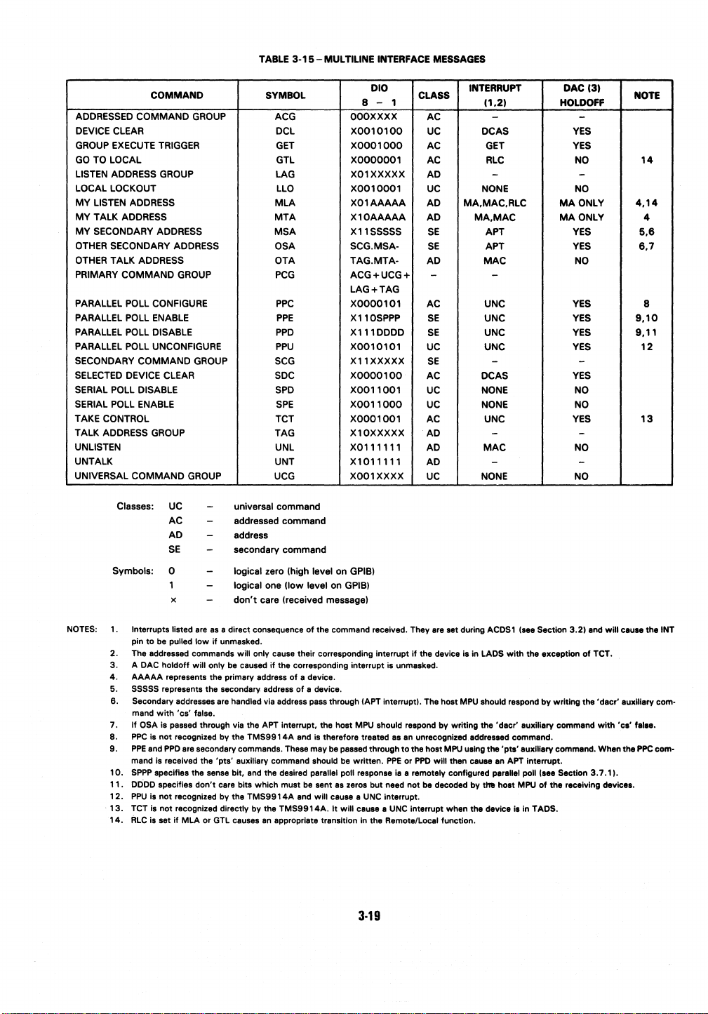
TABLE
3-15-MULTILINE
INTERFACE MESSAGES
COMMAND
ADDRESSED COMMAND GROUP
DEVICE CLEAR
GROUP EXECUTE TRIGGER
GO
TO LOCAL GTL
SYMBOL
ACG OOOXXXX AC
DCL
GET
LISTEN ADDRESS GROUP LAG
LOCAL LOCKOUT LLO
MY
LISTEN ADDRESS
MY
TALK ADDRESS
MY
SECONDARY ADDRESS
OTHER
SECONDARY ADDRESS OSA SCG.MSA-
OTHER
TALK ADDRESS
PRIMARY
PARALLEL
COMMAND GROUP
POLL CONFIGURE
PARALLEL POLL ENABLE
PARALLEL POLL DISABLE
PARALLEL POLL UNCONFIGURE
SECONDARY
COMMAND
GROUP
SELECTED DEVICE CLEAR
SERIAL POLL DISABLE
SERIAL POLL
ENABLE
TAKE CONTROL
TALK ADDRESS GROUP
MLA
MTA
MSA
OTA
PCG
PPC
PPE
PPD
PPU
SCG
SOC
SPD
SPE
TCT XOOO1001
TAG
UNLISTEN UNL
UNTALK
UNIVERSAL COMMAND GROUP
UNT
UCG
DIO
B-1
X0010100
XOO01000
XOOOOO01
X01XXXXX
X0010001
X01AAAAA
X10AAAAA
X11SSSSS
TAG.MTAACG+UCG+
LAG + TAG
XOOO0101
X110SPPP
X111DDDD
X0010101
Xl1XXXXX
XOOOO100
XOO11001
X0011000
X10XXXXX
X0111111
X1011111
XOO1XXXX
CLASS
INTERRUPT
11,21 HOLDOFF
- -
UC
AC GET YES
AC
AD
UC NONE NO
AD MA,MAC,RLC
AD
SE
SE
AD
-
AC UNC
SE
SE
UC UNC
SE
AC DCAS
UC NONE NO
UC NONE NO
AC
AD
AD
AD
UC NONE NO
DCAS
RLC
- -
MAONLY
MA,MAC
MAONLY
APT YES
APT
MAC
-
UNC
UNC YES
- -
UNC
- -
MAC
-
DACI31
YES
NO
YES
NO
YES
YES
YES
YES
YES
NO
-
NOTE
14
4,14
4
5,8
8,7
8
9,10
9,11
12
13
NOTES: 1.
Classes:
UC universal command
AC eddressed command
AD
SE
Symbols:
0
x
Interrupts listed
pin
to
2.
The addressed commands will
3.
OAC
A
4.
AAAAA
5.
SSSSS
6.
Secondary addresses are
mand
7.
If
OSA
8.
PPC
is
9.
PPE
and
mand
10.
SPPP
11.
DODD
12.
PPU
Is
13.
TCT is not recognized directly by the
14.
i8
flLC
are
as
be pulled
holdoff will only be caused
represents the primary address
represents the secondary
with
'cs' fals8.
Is
passed through via the APT interrupt, the host MPU should respond by writing the 'dacr' auxiliary command
not
recognized by the
PPO
Is
received the
specifies the sense bit,
specifies
not
recognized by the
set
If
a direct consequence
low
if
unmasked.
are secondary commands. These may
'pts'
don't
care bits which must
MLA or GTL causes
address
sacondary command
logical zero (high level on
logical one (low level on
don't
care (received message)
of
only cause their corresponding interrupt If the device
if
the corresponding interrupt is unmasked.
of
a device.
addreu
of
handled via address pass through IAPT Interrupt). The host
TMS9914A
auxiliary command should
and
the desired parallel poll response la a remotely configured parallel poll I
TMS9914A
an
a device.
end
be
and will cause a
TMS9914A.
appropriate transition
GPIB)
GPIB)
the command received. They
Is
therefore treated
be
pasled through
be
s.nt
as
zeros but need
It
will cause a
aa
en
to
written.
UNC
In
the host
PPE
or
PPO
not
Interrupt.
UNC
Interrupt when the device
the RemotelLocal function.
are
set during
ia
MPU
unrecognized addressed command.
MPU
using the
will then cause an APT Interrupt.
be
decoded by tha host
ACOS
in LADS
with
should respond
'pta'
1 Is
••
Section
3.2)
the exception
by
writing the 'dacr' auxiliary com-
auxililry
command. Whan the
...
Section 3.7.11.
MPU
of the receiving deviclS.
i.
In TAOS.
and will
of
TCT.
with
cluse
the INT
'ca' false.
PPC
com-
3-19

4.
TMS9914A
ELECTRICAL SPECIFICATIONS
4.1
ABSOLUTE
MAXIMUM
RATINGS OVER OPERATING FREE-AIR TEMPERATURE RANGE
(UNLESS OTHERWISE NOTED)*
Supply
voltage, VCC (see Note 1) . . . . . . . . . . . . . . . . . . . . . . . . . . . . . . . . . . .
All
input
and
output
voltages . . . . . . . . . . . . . . . . . . . . . . . . . . . . . .
Continuous
Operating free-air temperature range
Storage temperature range
..
Stresses beyond those listed under
operation
not
implied. Exposure
1:
Under absolute
NOTE
4.2
RECOMMENDED OPERATING CONDITIONS
Supply voltage,
Supply voltage,
High-level input voltage,
Low-level input voltage,
power
dissipation
.....................................................
............................................
...............................................
of
the
device
at
to
maximum
"Absolute
these
or
any
absolute-maximum-rated conditions
ratings voltage values arB
Maximum
other
conditions beyond those indicated in the
Ratings"
may
for
extended periods may
with
respect
cause permanent damage
to
VSS.
"Recommended
affect
device reliability.
to
the
device. This is a stress rating only and functional
Operating Conditions" section
VCC
VSS
VIH
VIL
VSS-0.3
Operating free-air temperature, T A 0
4.3
t
ELECTRICAL CHARACTERISTICS OVER FULL RANGE
PARAMETER
(any
at
TA = 25·C
Except
REN,IFC,INT
REN,IFC
only
input)
(any
input)
and nominal voltage.
VOH
VOL
II
ICC
Ci
All
typical values are
High-level
output voltage
Low-level output voltage
Input current
V
CC
supply current
Input capacitance
OF
RECOMMENDED OPERATING CONDITIONS
TEST
CONDITIONS
4OO
-
-
MHz,
1OO
I'A
I'A
VCC
unmeasured
IOH
IOH
IOL
VI
= 2 V to
= 1
f
=
=
= 2 mA
pins at 0 V
MIN
4.75
.. -0.3 V to
..
. . .
.. -0.3 V to
0
-
55°C
of
this specification is
NOM
5
0
2
MIN
VCC+
Typt
2.4
2.2
VSS
20
20
0.8
°C
to
70°C
to
150°C
MAX
UNIT
5.25 V
1
0.8
70
°c
MAX
UNIT
VCC
VCC
0.4
±10
150
15
I'A
mA
pF
V
V
W
V
V
V
V
V
4.4
TIMING CHARACTERISTICS
AND
REQUIREMENTS
Timing characteristics and requirements are given in Section
are
shown
in Figure 4-1
through
Figure
4-9.
4-1
4.4.1
through
Section
4.4.6;
relevant
timing
diagrams

4.4.1
Clock and
Host
Interface
Timing Requirements
Over
Full Range
of
Operating Conditions
t
c
tw(4)H)
tw(4)L)
tsu(AD)
tsu(DBIN)
tsu(CE)
tsu(WE)
tw(WE)
tsu(DA)
thIDA)
th(AD)
th(DBIN)
th(CE)
tsu(GR)
th(GR)
4.4.2
ta(CE)
ta(DBIN)
tsu(AD)
tz(DBIN)
tz(CE)
ta(GR)
tz(GR)
td(GR/RO)
(4))
PARAMETER MIN TYP
Clock cycle
Clock high pulse
Clock
Address setup
DBIN
CE
WE
WE
Data setup
Data hold
Address
D81N
CE
ACCGR setup
ACCGR hold
Host
Interface Timing Characteristics Over Full Range
low
setup
setup
setup
low
hold
hold
pulse
time
time
pulse
time
time
hold
time
time
time
width
width
time
time
width
time
time
time
PARAMETER
time
from
Access
Access
time
Address setup
time
Hi-Z
Hi-Z
time
time
Access
Hi-Z
time
Delay
of
ACCRQ high
CE
from DBIN
time
to
from
DBIN
from
CE
from
ACCGR
from ACCGR
CE
from
Al:a3f1
of
Operating Conditions
MAX
200
100
2000
1955
45
0 ns
0 ns
100
0 ns
80
60
0 ns
0 ns
0 ns
80
100
80
MIN
TYP
MAX
150
150
0 ns
50
100
50
100
150
100
50
100
UNIT
ns
ns
ns
ns
ns
ns
ns
ns
ns
UNIT
ns
ns
ns
ns
ns
ns
ns
4.4.3
td1
td2
td3
td4
td5
NOTES:
Source Handshake Timing Characteristics Over Full Range
PARAMETER TEST CONDITIONS MIN
Delay
of
DAV
true
from
of
write
operation
out
register
data
Delay
of
valid
GPIB
data lines from end
write
cycle
Delay
of
BO
interrupt
end
to
of
Normal
T1
Short T 1 (see Note 2)
Very short T 1 (see Note 2)
BO
interrupt
from DAC true unmasked
Delay
of
ACCRO DAC true
Delay
of
DAV
false
from
DAC true
1,
The
timing
of
the
2.
A
longer bus
occurs.
very
short
source handshake is
bus
settling
settling
time
time
takes
IT
1)
place
the
occurs
on the second and
jf
'stdl'
same
whether
is
set
unless there is a
ATN
is true or false, i.e"
subsequent
very
4·2
of
Operating Conditions (see
(see Note 2)
whether
data
short
byte
bus
sent
settling
when
time.
the
ATN
In
all
Note
12(4)) I
8(4))1
4(4))1
device is in
is
TACS,
false
if
the
other
instances, a normal bus
1)
12(4))1
8(<1»1
4(<1»1
CACS, or SPAS,
'vstd
l'
feature
MAX
UNIT
+310
+310
+310
ns
ns
ns
140
ns
ns
300
300
ns
160
ns
is set. A s,lightly
settling
time
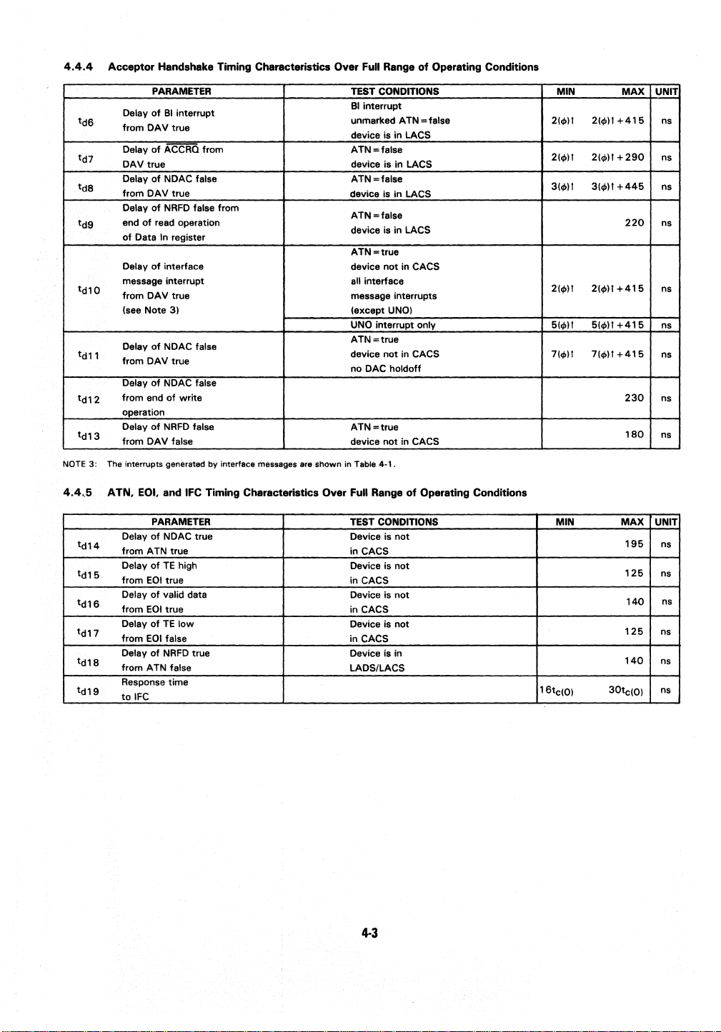
4.4.4
Acceptor Handshake Timing Characteristics Over Full Range of Operating Conditions
PARAMETER TEST CONDITIONS MIN
Delay
of
BI
td6
td7
tdB
td9
tdl0
td11
td12
td13
NOTE 3: The interrupts generated
4.4
from
Delay
DAV true device is in LACS
Delay
from
Delay
end
of
Delay
message interrupt all interface
from
(see
Delay
from
Delay
from end
operation
Delay
from
..
5 ATN. EOI. and IFC Timing Characteristics Over
interrupt
DAV
true
of
ACCRO from
of
NDAC false
DAV
true
of
NRFD
false from
of
read operation
Data
In
register
of
interface
DAV
true
Note
31
of
NDAC false
DAV
true
of
NDAC false
of
write
of
NRFD
false
DAV
false device not in CACS
by
interface messages are shown
BI
interrupt
TN
is
4-1.
= false
in LACS
LACS
LACS
CACS
CACS
off
unmarked A
device
ATN=false
ATN=false
device is in
ATN
=false
device is in
=true
ATN
device not in
message interrupts
(except UNOI
interrupt only
UNO
ATN
=true
device not in
no
DAC hold
ATN=true
in
Table
Full
Range of Operating Conditions
2(cf>lt 2(cf>lt
2(cf>lt
2(cf>lt + 290
3(cf>lt 3(cf>lt
2(cf>lt+415 ns
2(cf>lt
5(cf>lt
5(cf>lt+415 ns
7(cf>lt 7(cf>lt
MAX
+415
+445
220
+415
230
180
UNIT
ns
ns
ns
ns
ns
ns
ns
td14
td15
td16
td17
td18
td19
PARAMETER TEST CONDITIONS MIN
Delay
of
NDAC true Device
from A
TN
true
Delay
of
TE
high Device is not
from
EOI
Delay
from
Delay of
from
Delay
from A
Response time
to
true in CACS
of
valid data
EOI
true
TE
low
EOI
false in CACS
of
NRFD
true
TN
false
IFC
is
not
CACS
in
Device is
in
Device
Device is in
LADS/LACS
CACS
not
is
not
4-3
16tcIOI
MAX
195
125
140
125
140
30tc(01
UNIT
ns
ns
ns
ns
ns
ns

4.4.6
Controller Timing Characteristics Over Full Range
of
Operating Conditions
td20
td21
td22
td23
td24
td25
ld26
td27
PARAMETER
Delay
of
A TN true
from end
aux command
Delay
from end
aux command
Delay
from end
aux command
Delay
from end'
aux command
Delay
rpD
Delay
rDD
Delay
aux command cleared
Delay
sts aux command
of
tca
of
BO
interrupt
of
tca
of
ATN true
of
tcs ,
of
BO
interrupt
of
tcs
of
EOI
true from
aux command set
of
EOI
false from
aux command cleared
of
EOI
from rpp
of A TN
falsa from
TEST CONDITIONS
80
unmaskad
device is in ANRS
BO
unmasked
device is
BO
Device is not in
SDYS
in
ANRS
unmasked
orSTRS
18t
18t
8t
8t
8t
MIN
(0)
c
(0)
c
(0)
c
(0)
c
(0)
c
MAX
10(<1>)1 + 220
22(<1>)1 + 415
10(<1>)1 + 220
22(<1>)1 + 415
230
230
10(<1>)1
+415
210
UNIT
ns
ns
ns
ns
ns
ns
ns
ns
,It
I
14
I
14
FIGURE
tW(<I>H)
4·1-TMS9914A
~
I I
~
14
tel<l»
CLOCK
CYCLE
twl<l>U
TIMING
If
I
~I
I
~

D~
____________
Wi
_--'11'1
~
,-
-JJ1
t
...
IWEI
\11..--.._
1III~t-------teIDBINI------~~
I
__
--1.te~.---teICEI'-----~
1 I
~tIIDBINI
00-D7
RSO-RS2
_____
____
~tau(ADI---lol'----------1-1
roo-
.L.!
-"""'I)>--------------«'--
\!
...
---., I
I
--JX
VAliD
ADDRESS
FIGURE
4-2-TMS9914A
READ
CYCLE
1,If
___
__
TIMING
...J
'----i
~
V_A_L1_D_D_AT_A
___
I
tz(CEI
.J)
HI-Z
DO-D7
tsulDAl'
__
thiDAI'
'and
thlADI are only applicabla
---Jx~
to
the first eignal
FIGURE
to
become inactive, whether
4-3-TMS9914A
___
WRITE
CYCLE
4-5
it
Is
We
TIMING
x=
or
Ce.

ACCRa
\
A
~tcIGR/Ral----.j
NOTE
ACCGR
DBIN
WE
DO-D7
4:
A write enable pulse may occur
pressed
at
the TMS9914A.
~
,
,
I
\
,
I
I I
, \ Isee "
I
,
I
,
,
I
I
,
I
,
14
14
In a OMA
read operation. A write enable pulse may therefore be provided
FIGURE
talOBINl--li!
talGRI
4-4-TMS9914A
\
~
~
DMA
READ
rtwIWEI
NOTE
41
\:.:._...J
OPERATION
Ii
I
,
I
I
,
I
,
,
:
i+--tZIGRI----.j
~
/
HI-Z
~
for
system memory and need not be sup-
11-,
--_--'
~
~_,jl4-~----:-l--~'
OBIN
----~
00-07
____________________________________
• tsulDAI and thlDAI are only applicable to the first signal to become inaCtive, whether it
I :
--J)x(~
FIGURE
4-5-TMS9914A
DMA
WRITE OPERATION
4-6
,
""---
~G"
14--
tsulDAI"
It---
I ,
________
is
WE
1 i
thIDBINI=-1
-.~.-~
~
tsuIDAI"---I~~I4""thIDAI"--.j
V_A_L_IO_O_A_T_A
or
ACCGii.
thlDAI"
_________
L
--IJI
~

Ce~----7
WE
U
~td2
Dloa.DI01------+-!
s
o
U
R
C
E
DAV
\ I
'\. __
~
....
I
_____________________
..1/
~
'-lZTmzm
NDAC
A
C
C
E
INT
P
T
0
R
-----------------------+~
ACCRa
ACCGR
CE
---------------------------------~\
td1-l\
_
I.tcl5~
T :
/r----
I I
I I
:
\~_:~_--+:
~tcla---tl
:
~~-~:-----
i4'tcl9'1
--<,.....--
I
I I
I
'\---------/
I
j4-tcls4I
I
\~
j..
tcl7-tj
....
__
NOTESI
____'/:
,
I
~I
-------
I
~
'---II
---
-"r--------
NOTES:
5.
The interrupt line is taken
6.
The interrupt line is taken
FIGURE
low
by
a
BO
by a
interrupt.
BI
interrupt.
low
4·6 -TMS9914A
SOURCE AND ACCEPTOR . HANDSHAKE TIMINGISI
4-7
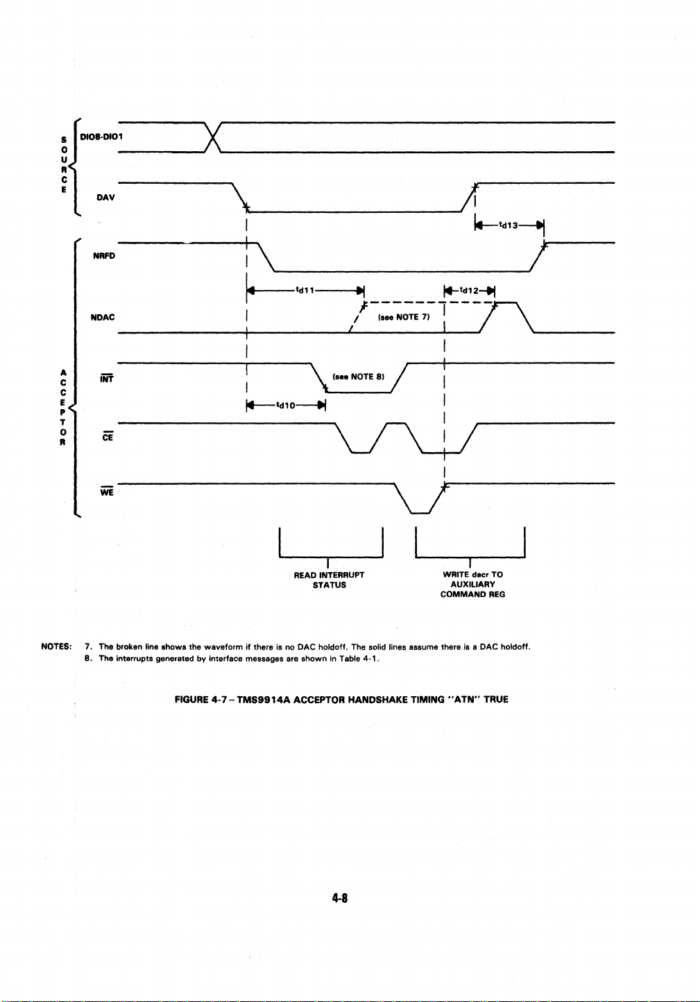
•
o
U
R
C
E
____
DAV
~x~
________________________
\"--
___
I
NRFD----~---+:'"'\\
L
-~
tct11--alt/
__
-----I;T
Ie-tct13~
/1.-----
I4-td12~
A
C
C
E
p
T
o
R
NOTES:
NDAC
7. The broken
8.
The Interrupti generated
Rne
shows
FIGURE
~
I4--tct10~
the waveform
by
if
thare
interface messages are shown
4-7-TMS9914A
Is
/-(:::~-7~1---T\-·
,
\
(_
NOTESI
V\l!
READ INTERRUPT
STATUS
no
DAC
holdoff. The solid lines assume there
In
Table
4-1.
ACCEPTOR
HANDSHAKE TIMING
/ :
V
I
I.
I
I
WRITE decr TO
AUXILIARY
COMMAND
Is a DAC
"ATN"
REG
TRUE
holdoff.
~.
____
_
4-8

ATN
\t:--
EOI
___
---I;1
I I
I
\~
__
~----~I-----------------
;1
:
1..-aI1d15
TE
----r-----r'----/
NRFD
NDAC
\ /
"---..
-'---'
Hld14
DAV
~HloZ---r--'r
I+-td16~
-~
\~_HIOZ
~
I I
: \
t
j..-
d17-.j
_____
/
HIOZ
__
--':
_____
I
I 'see
NOTE
91
,--
____
IV
\.-td1S--tl
\ _____
\~---__r_:
I
,-----
---Jif
I
---
D10SODI01--------c<--------)r----+----
d19
j+-t
..j
IFC
INT
Isee
NOTE
1~'--_....,..:
_____
I
,
'\1\....-1
__
_
_
_
NOTES:
90
This assumes that
10.
IFe causes the
an
RFD
TMS991SA
holdoff occurs.
to
be
unaddressed and
FIGURE
4-8-TMS9914A
an
IFe interrupt occurs.
RESPONSE TO
4-9
'ATN'
AND
'EOI'

ATN
rtd27~
\~------------~:
~
td20.
td22
~
td25
;--
I
NOTE
EOI
CE
WE
11: A BO
tcs or tea
interrupt
WRITE
occurs as
the
TMS9914A
READ INT
STAT 0
enters CACS.
FIGURE
SET
rpp
4·9-TMS9914A
\L...-----'--II
t
I4---tI
d24
I
'--_--'I
CLEAR
rpp
CONTROLLER
TIMING
;r----:----
..... 1 _---'
WRITE
Sts
4·10

5. MECHANICAL SPECIFICATIONS
5.1
TMS9914AJL-
Ceramic packages
Ii
L
15.24±0.254
rr(0.600±0.010)~
40-PIN CERAMIC PACKAGE
with
side-brazed leads and metal, epoxy, or glass lid seal
Ii
J
1.016 (0.0401 MIN •
SEATING1~4'089(0'161)MIN
F9
-PLANE
T~
0.254
(0.010)
5.2
NOMJL
0.457,.
(0.018,.0.002)
NOTES:
TMS9914ANL-40-PIN
~LWPIN
0.051 (See Note
a.
Each pin centerline Is located
b.
All linear
govern.
PLASTIC PACKAGE
~
~
. ®
~,{
~
~
~
~.
SPACING
dimension.
are In
::::::
0)
~ ~
~
~
~ ~
2.5410.100)
within
millimeter.
T.P.
a)
0.264
10.010)
and parenthetically In Inches. Inch dimensions
51.3112.020)
MAX
[~~]:::::::I
~ ~
~
~
~J
~
I~I
~
1.27
(0.060)
NOM
of
Its true longitudinal position.
~
~@)
~
~
RJ3.175(0.125)MAX
---.I
~7±0.508
10.050 ± 0.020)
Plastic packages
NOTES:
a.
Each pin centerline is located
b. All linear dimensions are in millimeters and parenthetically in inches. Inch dimensions
govern.
EITHER
INDEX
within
CD-----------------------------+·~
2.41
10.095)
1,4010.055)
0.254
10.010)
of
its
true longitudinal position.
5-1

APPENDIX A
IEEE-488 STANDARD CONNECTOR
SHIELD
SRQ
ATN
GND
11
LOGIC GND
GND
10
IFC
GND
9
NDAC
NRFD
GND REN
GND
8
DAV
DI04
DI02
EOI
DI03
DI01
DI07
DI05
7
GND
DI08 DI06
6
A-1

APPENDIX B
~
___
C_p_U
____
sic
sic
BO
TYPICAL
~11
SEQUENCES
~
____
C_O_N_T
____
OF
EVENTS
~II
FOR
THE
CONTROLLER
~
_____
S._H_·
____
~II
~
____
O_T_H_E_R
ATN
____
~
wdot
BO
FIGURE
8-1-CONTROLLER
RFD.DAC
DAV
DAC
TAKING CONTROL
8-1

BO
gts
BI
nUn
CPU
II
CONT
CSBS
LISTEN
LACS
II
200nl
-.~=--
A.H.
II
OTHER
DAC
ATN
RFD
DAV
DAC
"ASSUME
BI
(+END)
tcs
BO
*CWAS inhibits ANRS
so rdin can occur before
is
set.
NO
HOLDOFF
....
ACRS.
ATN
CSBS
CAWS
FIGURE B-2 - CONTROLLER
SIDS
LACS
LADS
AIDS
AS
A LISTENER (GOING TO STANDBY)
RFD
DAV
DAC
ATN
RFD
Dic
8-2

~
BO
gts
BO
wdot
BO
____
C_p_U
____
~1
~I
_____
___
C_O_N_T
____
"'_10
-II
~I
_____
S_._H_·
____
~I
~I
____
TA
__
LK_E_R
____
~I
~I
____
O_T_H_E_R
____
~
DAC
ATN
RFD.DAC
DAV
DAC
BO
wdot
BO
*Momentary
transition
following
BO
FIGURE
interrupt
may
B-3-CONTROLLER
not
occur
on
the
TMS9914
AS
A TALKER IGOING
8-3
but
is guaranteed
TO
STANDBY)
on
the
ATN
RFD.DAC
DAC
TMS9914A.

I
BO
CPU
I
CONT
I
S.H.
I
OTHER
OAC
rpp
rept
t9
FIGURE
8-4
- CONTROLLER PARALLEL POLLING
lOY
8-4

APPENDIX C
SN75160/161/162
Texas Instruments
and the bus controller. These transceivers may
GPIB
controllers commercially available. They provide the simplest method
part is tailored
With
layout.
SN7
5160A
speeds,
as
All transceivers in the SN7
mination
the
network
transceiver, the output presents a high impedance
hysteresis
SN75160
family
of
bus transceivers are designated
be
to
either the B-line data bus or B-line control bus, so they require no extra logic or complicated board
the
SN75160
series is pin-for-pin compatible
shown in Figure
required by
for
additional noise margin.
MAX
SPEED
{nsl
family,
it
takes only
with
C-l.
51
60
family have several features in common.
IEEE
Standard
60
50
40
30
20
10
488.
DATA
used
with
the TI
two
20-pin
DIP
the original SN7
This termination
to
the bus. Also, each receiver has a minimum
SHEETS
TMS9914
packages
51
is
designed so
~
____
to
provide the interface between the bus
Bus Controller chip or any
of
60
series but
Each
interfacing
to
get
driver
that
4750
1625
pJ
on the
with
output
when power
pJ
to
the
bus, because each
GPIB.
The
lower
power and faster
has built
is
new
into
removed from
of
the other
improved
it
the ter-
of
400
mV
40
The
SN75160A
(TE)
Enable
fron the bus and transferred
transmit mode, and data will
tively drive the bus high or
put
which, when taken
is designed
to
implement
input. All eight channels are simultaneously in the receive mode when
to
the bus controller. When the
be
transmitted onto the bus.
low
to
give the fastest data rates possible. The
low,
disables the upper stage
collector type outputs. The open-collector
but
it
does allow more than one instrument
parallel polling where up
eight-line data
for
regular data transmission.
The
SN7
with
the Talk-Enable
direction
SRQ,
have ope.n-collector driver outputs
bus, greatly speeding the polling process. They may then
5161
A is used
for
exchange
to
eight instruments may
to
implement
(TE)
and Direction Control (DC) inputs, insures
of
bus management and handshaking signals. Three
the
the
output
8-line control bus. Included in
as
60 100 120 140 160
60
MAX
PWR/CHANNEL
FIGURE
C-'
B"line data bus. The direction
{nWI
of
TE
is
in
the high state, all eight channels go
Each
driver features a totem-pole output which can ac-
SN75160A
of
the driver outputs turning all eight driver outputs into open-
mode does
to
be
transmitting on the bus at the same time. This feature is used in
be
not
allow
as
fast a data rate
polled simultaneously, each responding on one line
be
switched back
it
is the necessary logic which, combined
that
each channel is enabled in the correct
of
required by the
IEEE
Standard
488.
wired-OR configuration. The other five channels have totem-pole outputs. The
method
of
implementing the control bus. The
the
REN
and
IFC
flexibility, control
systems). Because
channels is controlled by a separate input called the System Controller (SCI.
of
the entire Bus System may
of
this extra input, the
SN75162A
be
transferred from one instrument
SN75162A
is identical
package has
to
22
the
SN75161
pins.
C-1
data
flow
is controlled by the Talk
the
TE
is
low
and data is received
has a Pull-up Enable
as
with
the totem-pole,
to
the totem-pole mode
the channels, NDAC,
NRFD,
These lines are always used
SN7
5162A
A except
to
offers
an
that
the direction
With
this additional
another (multiple controller
to
the
(PE)
in-
of
the
and
in
alternate
of
a

features
SN75160A,
SN75161A
IEEE-488
GPIB
AND
BUS
TRANSCEIVERS
• 8-channel bidirectional transceivers
• Maet
• Low power dissipation
•
• Receiver hysteresis
• Open-collector driver output option
IEEE
standard
High-impedance
PNP
488
1978
(65
mW max per channel)
inputs
(500
mV typ)
(SN75160A)
• Bus-terminating resistors provided on driver outputs
• No loading
• SN75161 A for single-controller systems;
of
bus when device is powered
down
(Vee
SN75162A
SN75162A
= 0
OCTAL
V)
for multi-controller systems
NOTE: Integrated Schottky-Barrier diode-clamped transistor is patented by Texas Instruments. U.S. Patent Number
3.463.975.
description
These octal bus transceivers are designed
between operating units
SN75162A
in systems
terminating resistors so
When
PE
is low. the bus outputs
three-state ports when
the bus lines.
and
of
the instrumentation system. The sixteen signal lines are normally required
with
more than one controller. An active turn-off feature has been incorporated into the bus-
that
the devices exhibit a high impedance
of
PE
is high. Taking
enables the D outputs.
the
SN75160A
TE
to
provide communication
have the characteristics
low
places those ports in the free-state. wherein they can
on
the genaral-purpose interface bus
to
the bus whan
Vee
of
open-collector outputs. They act
= 0 V.
absolute maximum ratings over operating free-air temperature range (unless otherwise noted)
Supply voltage.
!nput voltage
Vee
(see
Note 1)
..............•......................................
...............................•.................................
Low-level driver output current . . . . . . . . . . . . . . . . . . . . . . . . . . . . . . . . . . . . . . . . . . . . . . . .
Continuous
Operating free-air temperature range
total dissipation
at
(or below)
25
°e
free-air temperature
............................................
(see
Note 2)
................
Storage temperature range. . . . . . . • . . . . . . . . . . . . . ... . . . . . . . . . . . . . . . . . . . . . . . . -
Lead
NOTES:
temperature
1. All voltage values
2.
For operation above
1/16
inch
(1.6
mm) from case for
are
with
respect
to
25·C
free·air temperature. derate linearly
network ground terminel.
10
seconds
at
the rate
..........................•..
of
9.3
mWI C to
740
mW
at
70·C.
65
be
driven
... 1 00
11
0
°e
to
°e
to 1
(GPIB)
by
5.5
50
mW
70
50°C
260
the
as
by
7 V
V
mA
°e
°e
C-2

table
of
abbreviations
CLASS NAME IDENTITY
CONTROL
INPUTS
SN75161A
1/0
PORTS
SN75161
SIGNAL
MNEMONICS
A/162A
SN75160A
DC
PE
TE
B Bus side
D
ATN
DAV
EOI
IFC
NDAC
NRFD
REN
SRO Service Request
SC
N
DUAL-IN-LINE
PACKAGE (TOP VIEW)
Direction Control
Terminal side
Not
Not
System Controller
Pull-up Enable
Talk Enable
of
device
of
device
Attention
Data Valid
End
or
Identify
Interface Clear
Data Accepted
Ready for Data
Remote Enable
SN
7 51
6DA
function table
INPUTS OUTPUTS INPUTS OUTPUTS
TE
0
H
H
L H H L H L X
H X
L H L L
L
X
F = free
state",
'H
"This
is the high-impedance state
modified by the internal resistors
= high level, L =
VCC
06
07
08
PE
BUS
DRIVERS
TE
B1
B2
B3
B4
B5
B6
B7
sa
GND
B B TE
H H L L X
L F
X H
X F
low
level, X = irrelevant, Z = high-impedance state.
of
a normal 3-stato
to
Vee
and ground.
output
modified by the internal resistors
to
Vee
TERMINAL
RECEIVERS
PE
X
and sround.
0
L
H
Z
C-l

SN75161A N
BUS
DUAL·IN·LINE
PACKAGE (TOP VIEW)
TE VCC
REN
REN
IFC IFC
NDAC NDAC
NRFD
NRFD
TERMINAL
SN 7
51
61
A
function
TE
H H H
H H
H L X
L
L
L L L
H = high level, l =
t
ATN
is a normal transceiver channel
same state. When
* Direction
transfer is non inverting in
low
TE
and
of
data transmission is
DAV
EOI
ATN
SRO
GND
table
CONTROLSt
ATN
DC
LEVEL
EOI
DIRECTION
R T R R T
L
R R R R T
T T T T R
H X
L
H
R R R R T T
R T
T
T T T T R
level, R = receive, T = transmit, X = irrelevant
DC
both
that
are in opposite states,
directions.
functions additionally
from
the terminal side
as
an
the
ATN channel functions
to
internal direction control or talk enable
the bus side, and the direction
DAV
EOI
ATN
SRO
DC
DIRECTION OF
REN
IFC
SRO
T R T T R
as
an independent transceiver only.
of
data receiving is
DATA*
NRFD
NDAC
R R T
R R T
R R T
T R
T T R
for
EOI
whenever
from
the bus side
DAV
the
TE
and DC inputs are in
to
the terminal side. Data
the
C-4
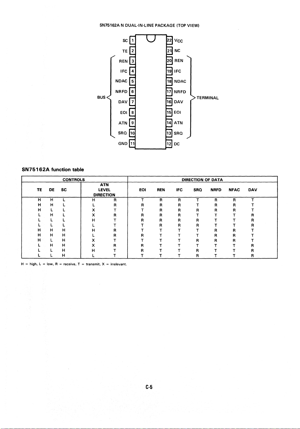
SN75162A N
REN
NDAC
DUAL·IN·LINE
PACKAGE (TOP VIEW)
SC
TE
IFC IFC
NC
REN
NDAC
SN75162A
TE
H H L
H
H L L
L H L
L L
L L L
H
H H H
H L
L H
L L H
L L
H = high, L =
BUS
NRFD
DAV
EOI
ATN
SRO
GND
function table
CONTROLS DIRECTION
DE
SC
H
L
L
H
H
H
H
H
low,
R = receive, T = transmit, X = irrelevant.
ATN
LEVEL
DIRECTION
H
L
X
X
H
L
H
L
EOI
R T
R R R R T R R T
T T R R R R R T
R
T R R R
T T R R R T T R
R T T T
R R T T T R R T
REN
R R
R R R T T T R
X T T T T R
X R R T T
H
L
T R T T R
T T T T R T T R
ATN
SRO
DC
IFC
TERMINAL
OF
DATA
SRO
NRFD
T R R
R
T
T T
R R T
R R
T T T
T T R
NFAC
DAV
T
R
T
R
C-5

functional
block
diagrams
~
____________________
SN75160A
TERMINAL
~A~
______________________
~
,/
DB
B8
(121
(9)
07
(131
181
B7
D6
1141
171
B6
"'-
~
____________________________
05
1151
161
B5
V
BUS
SN75161A
~A~
D4
1161
(51
B4
BUS
____________________________
03
(171
14)
B3
02
1181
(3)
B2
01
121
Bl
"'-
1191
/"
~
/ "'-
OAV
(6)
TE
OAV
",--------------------------~
NOAC
NOAC
(41
1171
NRFO
NRFD
(5)
1161
EOI
SRQ
(91
SRQ
(121
1131
ATN
~------------------------~/
V
TERMINAL
REN
REN
(21
1191
IFC
IFC
(31
DC
C-6

SN75162A
~
____________________________
-JA
_________________________________
BUS
~
/ ,
DAV
NDAC
(7}
15}
NRFD
SRO
(61
(10}
REN
(3}
IfC
(4}
TE
DAV
,,~--------~----------------~
switching
tpLH
tpHL
tpLH
tpHL
tpZH
tpHZ
tpZL
tpLZ
tpZH
tpHZ
tpZL
tpLZ
characteristics.
PARAMETER
Propagation delay time.
low-to-high-Ievel output
Propagation delay time.
high-to-Iow-Ievel output
Propagation dalay tima.
low-to-high-Ievel output
Propagation delay time.
high-to-Iow-Ievel output
Output enable
to
high level
Output disable time
from high level
Output enable
to
low level
Output disable time
from
low
level
Output enable
to
high level
Output disable time
from high level
Output enable
to
low level
Output disable
from
low level
Output pull-up
enable time
Output pull-up
disable time
NDAC
time
time
time
time
time
118}
Vee
FROM
Terminal
Bus
TE
or
DC
TE
or
DC
PE
NRFD
5 V.
Terminal
Terminal
Terminal
EOI
15
eL
TO
Bus
Bus
pF.
TEST
CONDITIONS MIN TVP
CL=30
RL=38.311
to
2.3
CL=30
RL=240
to
5 V
RL=48011
toOV
RL=38.3
to
2.3
RL=3kll
to
0 V
RL=28011
to
0 V
RL
=480
to
0 V
SRO
17
17
16
16
DC
MAX
25
25
25
25
REN
SN75182A
MIN TVP
17
17
16
16
ATN
~-----------------------------~
V
TERMINAL
25°e
TA
pF
V
pF
II
II
V
II
(unless otherwise noted)
SN75180A
MAX
14
14
12
15
25
12
22
21
20
13
23
19
15
13
SN75181A
MIN TVP
20
20
20
22
MAX
25
25
25
25
IFC
SC
UNIT
ns
ns
ns
ns
ns
C-7

APPENDIX D
EXAMPLE SOFTWARE
DESIGN
EXAMPLE
DESIGN
STATEMENT
SYSTEM COMPONENTS
OBJECTIVES
• Illustrate
• Illustrate
over the
• Demonstrate the use
• Show
• Show the elements
• Show the hardware necessary
• TM9901101-based system
• Use the
• Configure
• Trigger the meter
• Decode the ASCII data into speech and provide a vocal annunciation
• Hewlett Packard model
- IEEE-488 compatible device
-
- Remote measurement trigger capability
• TI
-
-
- Up
-
-
• TI
-
- 1 80-word vocabulary
-
- Programmed through
-
-
• TI TMS9914-based interface board
- Designed
- Interfaces directly
the procedures
the procedures used
GPIB
bus
the software necessary
OF
THE
TMS9914
an
HP3455A
Range
and function selection locally selected and indicated in measurement data
TM990/1
TMS9900
4K
TMS9901 programmable system interface providing up
timer
Two
TM990/306
TM990
2.5
Serviced on interrupt or polled besis
Additional edge connector for interfacing
01
M microcomputer
16-bit
bytes
of
to
W amplifier for direct speaker drive
RAM mappable
8K bytes of
serial
110
speech module
series bus compatible
to
illustrate the interfacing
and
protocol
to
some other device.
of
the
TMS9914
of
hardware design which must be dealt
EXAMPLE
to
ports (RS232C compatible)
DESIGN
to
communicate
digital voltmeter
take a measurement
CHOSEN
3438A
CPU
EPROM
TMS9900
to
the components described above
of
the remote
to
configure a remote instrument
as
a controller. talker.
to
drive the
to
interface the
digital voltmeter
CPU
to
either the bottom or top
at
the bottom
TMS9914
PROBLEM
with
the
GPIB.
to
take two-wire resistance measurements.
and
module
of
CRU
interface
to
of
the
and
local messages used
to
and
listener.
when
it
is
interfaced
with
when interfacing the
TMS9914
send the data over the
memory space
non-TM990 devices
TMS9914
to
the
GPIB
of
the memory address space
to
16
prioritized maskable interrupts
to a CPU
to
configure a controller.
acquire data
bus.
GPIB
of
and
and
then transmit the data
to
TM990
products.
TMS9914
to
the
TM990
the resistance measurement.
to
the IEEE-488 DUS
to
system.
and
an
MPU.
interval
0-1

('-
...
;;
TM990/101
MICROCOMPUTER
BOARD
TM990
BUS
k'-
...
V'
~
PROGRAMMER'S MODEL
1
4-bit
•
- Bits
• 1 bit
• 1 bit
• 1 bit
to
-
Set
to
0 starts/enables speech
-
- 1 stops/disables speech
to
0 means speech board busy
-
- 1 means speech board
.....
~
....
,)
FIGURE
D-1-APPLICATIONS
OF
THE
address selects word
16
to
29
on the
CRU
enable
EPROM
to
1 during initialization
start/stop speaking
indicate the busy status
speech data
not
TM990!306
SPEECH
TMS9914 GPIB
INTERFACE BOARD
TM990/306
to
speak
interface
busy
MODULE
TM990/512
of
speech board
HARDWARE BLOCK DIAGRAM
SPEECH
BOARD
Vi
i't
IEEE-488
BUS
~
V
DIGITAL
VOLTMETER
METER
DATA
OUTPUT CHARACTERISTICS
•
Data
is
output
as
of
- Format
R indicates the range setting
•
'1' = DC
'2'
= AC volts
'3'=
'4'=
'5'=
•
EOI
message is sent
the string is + D.DDDE + D,R OD)A
volts
DC
amps
AC amps
ohms
a string
with
of
ASCII characters.
of
the
meter.
LINE
FEED
character.
0-2

TURN
OFF
SE
LECT EPROM
LOAD
WORD ADDRESS
TURN
ON SPEECH
SPEECH
YES
NO
NO
YES
FIGURE
TURN
OFF
SPEECH
0-2
- TYPICAL SPEECH BOARD USE
0-3
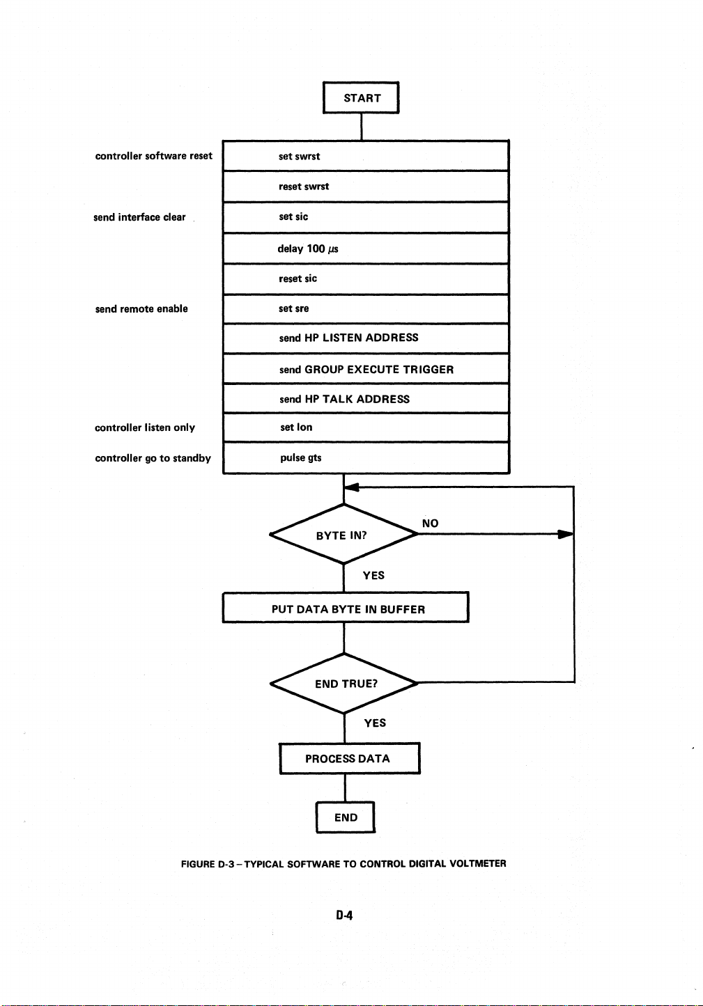
controller software reset
set swrst
reset swrst
send interface clear
send remote enable
controller listen only
controller go
to
standby
set sic
delay
100ps
reset sic
set sre
HP
send
send GROUP
send
set
LISTEN ADDRESS
EXECUTE TRIGGER
HP
TALK ADDRESS
Ion
pulse gts
PUT DATA BYTE
IN
BUFFER
NO
FIGURE
D-3-TYPICAL
SOFTWARE TO CONTROL DIGITAL VOLTMETER
0-4

SOFTWARE
LISTING
.. ..
..
..
..
..
..
..
..
..
..
..
..
..
..
..
..
..
*
..
BASE
IMASKO
ISTATO
IMASK1
ISTATl
ADSTAT
BUSTAT
AUXCMD
ADRSWI
ADDRES
SERPOL
CMDPAS
PARPOL
DATIN
DATOUT
*
*
..
INTO
INT1
31
EO
END3
SRQ
MASKO
IDT 'DEM3438A'
..
..
..
..
..
..
.. ..
GPIB
"TALKING
.. .. ..
TMS
EQU
EQU
EQU
EQU
EQU
EQU
EQU
EQU
EQU
EQU
EQU
EQU
EQU
EQU
EQU
T!1S
EQU
EQU
EQU
EQU
EQU
EQU
EQU
DEMONSTRATION
CONTROLLE:E\"
TMS9914
HP
3438A
TM990/306
..
..
9914 REGISTER
>5540
BASE+O
BASE+O
BASE+2
BASE+2
BASE+4
BASE+6
BASE+6
BASE+8
BASE+8
BASE+10
BASE+12
BASE+12
BASE+14
BASE+14
9914
INTERRUPT
>8000
>4000
>2000
>1000
>0800
>0200
BI+BO+ENDB
BASE
DEVICE
CRU
..
..
..
..
..
..
ADDRESS:
ADDRESS:
..
..
..
EQUATES
AND
.. ..
..
..
..
..
.. ..
..
..
..
THIS
REVISION 4/14-NOV-80/PNK
ADDRESS:
..
..
BASE
INTERRUPT
INTERRUPT
INTERRUPT
INTERRUPT
ADDRESS
BUS
AUXILARY
ADDRESS
ADDRESS
SERIAL
COMMAND
PARALLEL
DATA
DATA
POLLING
INTERRUPT
INTERRUPT
BYTE
BYTE
BYTE
SERVICE
D~ABLE
VERSION
..
..
ADDRESS
STATUS
FROM
TO
READY
READY
IS
FOR
>5540
>17
>lFEO
..
..
..
.. ..
OF
MASK
STATUS
MASK
STATUS
STATUS
REGISTER
CO~~D
SNITCH
REGISTER
POLL
tI.:ASKS
INTERRUPTS
REGISTER
PASS
BUS
LAST
REQUEST
POLL
BUS
REGISTER
GROU?
GROUP
FOR
FOR
THROUGH
PEGISTER
REGISTER
ONE
HP
..
..
TMS
0
0
1
1
REGISTER
REGISTER
"REGISTER"
0
1
INPUT
OUTPUT
GIVEN
..
.. ..
..
3438A
..
..
.. ..
9914
REGISTER
..
..
..
..
..
..
..
"
...
..
..
0·5

*
*
*
SWRST
SWRSTC
FEOI
LON
LONC
TON
TONC
GTS
TCA
SIC
SICC
SRE
SREC
*
*
*
GET
LLO
SDC
DCL
SPE
SPD
UNL
UNT
*
* HP3455A
*
HPLA
HPTA
*
*
*
*
RESET * DATA
SELECTED
EQO
EQU
EQU
EQU
EQU
EQU
EQU
EQU
EQU
EQU
EQU
EQU
EQU
SELEr.TED
EQU
EQU
EQU
EQU
EQU
EQO
EQU
EQU
EQU
EQO
AORG
INTERRUPT
DATA
TMS
9914
>8000
>0000
>0800
>8900
>0900
>8AOO
>OAOO
>OBOO
>OCOO
>8FOO
>OFOO
>9000
>1000
MULTILINE
>0800
>1100
>0400
>1400
>1800
>1900
>3FOO
>5FOO
DVM
ADDRESSES
>3700
>5700
>0000
VECTOR(S}
l<1A
I
NWS
START
AUXILARY
SET
CLEAR
FORCE
SET
CLEAR
SET
CLEAR
GO
TAKE
SET
CLEAR
SET
CLEAR
I/F
MESSAGES
GROUP
LOCAL
DEVICE
DEVICE
SERIAL
SERIAL
UNLISTEN
UNTALK
LISTEN
TALK
STARTING
INITIAL
INITIAL
COMMANDS
SOFTWARE
SOFT~qARE
END
OR
LISTEN
LISTEN
TALK
TALK
TO
STANDBY
CONTROL
SEND
SEND
SEND
SE:-tD
EXECUTE
LOCKOUT
ADDRESS
ONLY
ONLY
ONLY
INTERFACE
INTERFACE
REMOTE
REMOTE
CLEAR
CLEAR
POL~
POLL
COM...'1AND
ADDRESS
ENABLE
DISABLE
COMMAND
ADDRESS
W?
PC
RESET
RE
SET
IDENTIFY
ONLY
ASYNCHRONOUSLY
CLEAR
CLEAR
ENABLE
ENABLE
TRIGGER
(UNIVERSAL)
(ADDRESSED)
(UNIVERSAL)
(UNIVERSAL)
(UNIVERSAL)
(ADDRESSED)
(UNIVERSAL)
(UNIVERSAL)
D-8
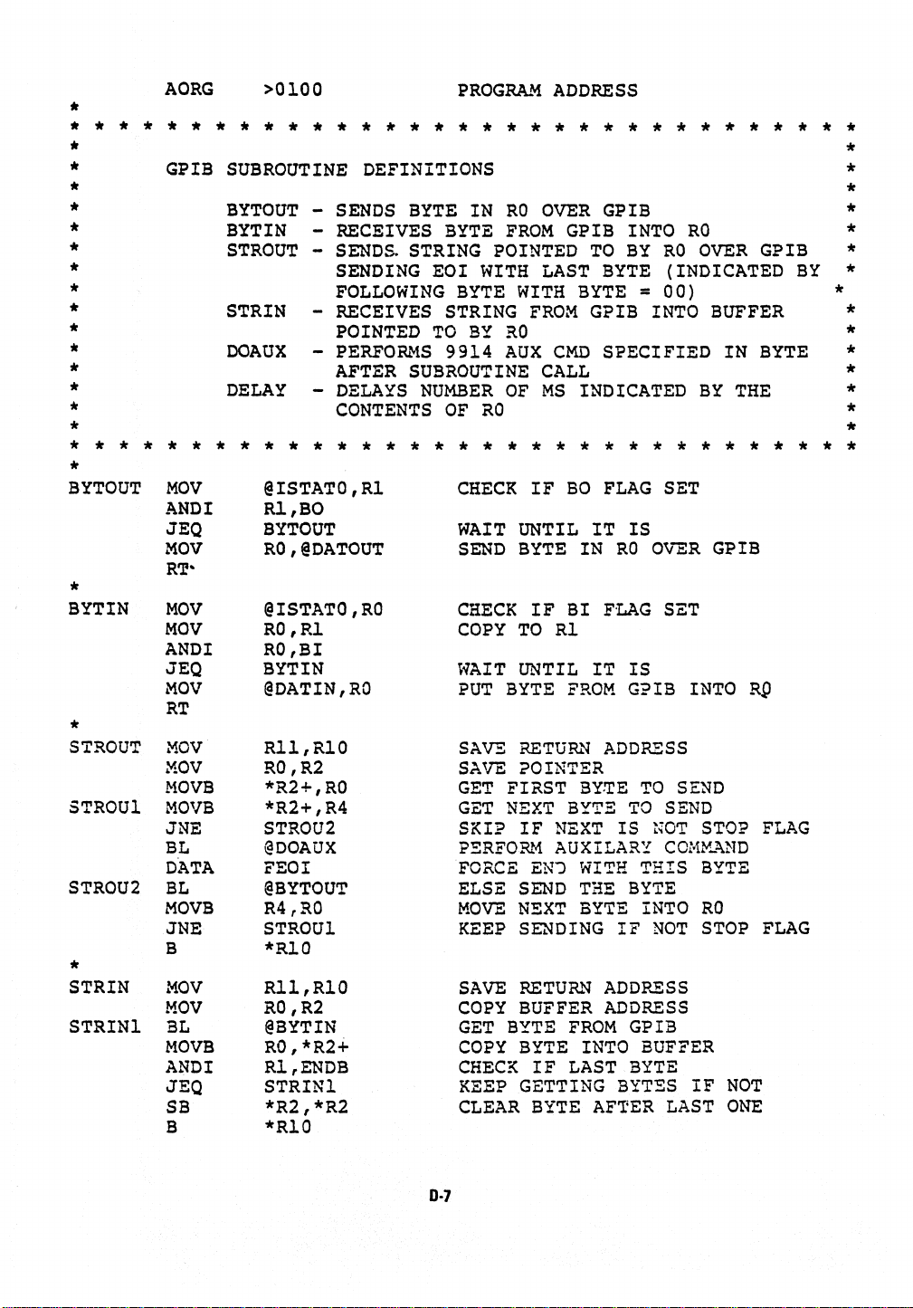
AORG
>0100
PROGRA.~
ADDRESS
*
* * * * * * * * * * * * * * * * * * * * * * * * * * * * * * * * *
* *
*
*
*
*
*
*
*
*
*
*
*
*
*
GPIB
SUBROUTINE
BYTOUT
BYTIN
STROUT
STRIN
DOAUX
DELAY
-
SENDS
-
RECEIVES
-
SENDS.
SENDING
FOLLOWING
-
RECEIVES
POINTED
-
PERFO&~S
AFTER
-
DELAYS
CONTENTS
DEFINITIONS
BYTE
STRING
SUBROUTINE
IN
BYTE
EOI
~UTH
BYTE
STRING
TO
BY
9914
NUMBER
OF
RO
RO
OVER
FROM
POINTED
RO
AUX
OF
GPIB
LAST
WITH
FROM
CMD
CALL
MS
GPIB
INTO
TO
BY
RO
BYTE
BYTE
GPIB
SPECIFIED IN
INDICATED
(INDICATED
= 00)
INTO
RO
OVER
BUFFER
BY
GPIB
BYTE
THE
BY
*
*
*
*
*
*
*
*
*
*
*
*
*
* *
* * * * * * * * * * * * * * * * * * * * * * * * * * * * * * * * *
*
BYTOUT
*
BYTIN
*
STROUT
STROUl
STROU2
*
STRIN
STRINl
MOV
ANDI
JEQ
MOV
R'r-
MOV
MOV
ANDI
JEQ
MOV
RT
MOV
MOV
HOVB
MOVB
JNE
BL
DATA
BL
MOVB
JNE
B
MOV
MOV
BL
MOVB
ANDI
JEQ
SB
B
@ISTATO,Rl
Rl,SO
BYTOUT
RO,@DATOUT
@ISTATO,RO
RO,Rl
RO,BI
BYTIN
@DATIN,RO
Rl1,
R10
RO,R2
*R2+,RO
*R2+,R4
STROU2
@DOAUX
FEOI
@BYTOUT
R4,RO
STROUl
*R10
Rll,R10
RO,R2
@BYTIN
RO,
*R2+
Rl,ENDB
STRINl
*R2,*R2
*R10
CHECK
WAIT
SEND
CHECK
COpy
~qAIT
PUT
SAVE
SAVE
GET
GET
SKIP
PERFORt4
FORCE
ELSE
MOVE
KEEP
SAVE
COpy
GET
COPY
CHECK
KEEP
CLEAR
IF
UNTIL
BYTE
IF
TO
UNTIL
BYTE
RETU&~
POINTER
FIRST
NEXT
IF
EN~
SEND
NEXT
SENDING
RETU~~
BUFFER
BYTE
BYTE
IF
GETTING
BYTE
BO
FLAG
IT
IS
IN
RO
BI
P'LAG
Rl
IT
IS
FROM
BYTE
NEXT
AUXILARY
FROM
LAST
G?IB
ADDRESS
BYTE
WITH
THE
BYTE
INTO
TO
TO
IS
THIS
BYTE
IF
ADDP~SS
ADDRESS
GPIB
BUFFER
BYTE
BYTES
AFTER
INTO
SET
Ov~R
NOT
NOT
GPIB
SET
INTO
SEND
SEND
STOP
COHK!l..ND
BYTE
RO
STOP
IF
NOT
LAST
ONE
R~
FLAG
FLAG
0·7

*
DOAUX
*
DELAY
DELOl
MOV
INCT
RT
LI
DEC
JNE
DEC
JGT
RT
*Rll,@AUXCMD
Rll
Rl,lSO
Rl
DELOl
RO
DELAY
SEND
BUMP
DELAY
DECREMENT
COUNT
DECREMENT
LOOP
AUX
CMD
RETURN
NUMBER
DOw'"N 1 MS
UNTIL
IN
ADDRESS
OF
MS
TIMER
MAIN
TIME
WORD
MS
IN
TIMER
IS
UP
AFTER
RO
CALL
*
* * * * * * * * * * * * * * * * * * * * * * * * * * * * * * * * *
* *
*
*
*
*
*
*
*
*
*
*
*
*
*
* *
*
TLKCRU
TLKBSY
TLKNTK
TLKEPM
*
TLKSET
*
TLKGO
*
TLKw'"RD
TLKWOl
TLKW02
TLKW03
TALKING
SUBROUTINE
TLKSET .-INITIALIZES
TLKWRD -SPEAKS
BY
MS
TLKSEN -SPEAKS
WHEN
DIGCVT -CONVERTS
INTO
REDTLK -SPEAKS
DATA
DEFINITIONS (TM990/306
WORD
(RO)
INDICATED
IF
SENTENCE
WORD
SPEECH
POINTED
TO
ASCII
VALUE
TALKING
AT
SPEECH
(Ra)
>= a OR
BY
-(Ra)
POINTED
SPEAK
ADDRESSES
OF
TO
IS
CODE
HP34S~A
BY
R2
BOARD)
ROUTINE
ADDRESS
IF
>FFFF *
FOR
WORKSPACE
INDICATED
DELAYS
eRO)
TO
DECIMAL
FORMATTED
NUMBER
< 0 *
BY
Rl,
DIGITS *
OF
HALTING
OUTPUT
*
*
*
*
*
*
*
*
*
*
* * * * * * * * * * * * * * * * * * * * * * * * * * * * * * *
EQU
EQU
EQU
EQU
LI
SBO
SBO
RTWP
DATA
DATA
MOV
ABS
JLT
LDCR
SBZ
TB
JNE
TB
JEQ
SEO
RTWP
BL
RTWP
>lFEO
-15
14
15
R12,TLKCRU
TLKEPM
TLKNTK
TALKi'lS
TLKSET
*R13,
RO
TLKW03
RO,14
TLKNTK
TLKBSY
TLKW01
TLKBSY
TLKW02
TLKNTK
@DELAY
RO
TM990/306
BUSY
T~.LK/NOTALK
TALK
INITIALIZE
SET
&~D
BLw'1?
GET
CHECK
SKIP
SELECT
TUR."l
WAIT
WAIT
TUR."l
PERFORI1
STATUS
EPROM
EPROH
TURN
XFER
WORD
IF
ON
FOR
FOR
OFF
BOARD
ENABLE
OFF
VECTOR
FROM
IF
WORD
DELAY
WORD
TALKING
306
306
TALK
DELAY
HI
BIT
BIT
ENABLE
TALK
CRU
TALKING
OLD
OR
TO
SPEAK
TO
START
TO
STOP
ING
CRU
BIT
BI'l'
WS
DELAY
BASE
ADDRESS
0·8

*
TALK
*
TLKSEN
TLKSOl
*
DIGCVT
DIGCOl
DIGC02
DIGTLK
*
REDTLK
REDTOl
REDT02
REDT03
REDT04
DATA
DATA
MOV
CI
JEQ
BLWP
JMP
RT
CI
JLT
CI
JLT
LI
RT
AND
I
SLA
MOV
RT
DATA
DATA
DATA
DA'1'A
DATA
DATA
DATA
DATA
DATA
DATA
MOV
MOVB
JEQ
SRL
CI
JEQ
CI
JNE
LI
JMP
CI
JNE
LI
JMP
CI
JNE
LI
BL
JMP
BL
TALKWS
TLKWRD
*Rl+,RO
RO,-l
TLKSOl
@TALK
TLKSEN
Rl,>30
DIGCOl
Rl,>3A
DIGC02
RO,-l
Rl,>OOOF
Rl,l
@DIGTLK(Rl)
>2E94
>06FC
>0900
>249A
>0372
>03CO
>35SE
>23~E
>02AC
>31C2
Rll,R10
*R2+,Rl
REDT07
RI,a
Rl,>2C
REDT06
Rl,>2D
REDT02
RO,>OF02
REDTOS
Rl,>2E
REDT03
RO,>2146
REDTOS
Rl,>4S
REDT04
Rl,ETOTHE
@TLKSEN
REDTOl
@DIGCVT
,RO
BLWP
COPY
QUIT
SAY
GET
CHECK
RETURN
XFER
WORD
IF
ONE
NEXT
IF
DELAY
ISOLATE
MULTIPLY
GET
SPEECH
ZERO
ONE
TWO
THREE
FOUR
FIVE
SIX
SEVEN
EIGHT
NINE
SAVE
GET
QUIT
RETU~~
BYTE
IF
ISOLATE
CHECK
SKIP
FOR
TO
CO:VIPARE
SKIP
IF
INDICATE
SKIP
J!...HEAD
COMPARE
SKIP
IF
INDICATE
SKIP
AHEAD
COMPARE
SKIP
SAY
AHEAD
"10
CONVERT
VECTOR
TO
P.O
STOP
WORD
FLAG
OR
DELAY
WORD
ASCII DIGIT
IF
NOT
BCD
VALUE
BY
2
VALUE
ADDRESS
TO
SPEAK
STOP
BYTE
BYTE
IN
LS
","
END
IF
SO
TO
"-"
NOT
"MINUS"
TO
"."
NOT
"POINT"
TO
"E"
IF
NOT
TO
~HE"
DIGIT
0-9

REDTOS
REDT06
REDT07
ETOTHE
UNITS
DCV
ACV
DCI
ACI
OHMS
*
BLWP
JMP
MOVB
ANDI
SRL
DECT
MOV
BL
B
DATA
DATA
DATA
DATA
DATA
DATA
DATA
DATA
DATA
DATA
EQU
DATA
DATA
DATA
DATA
DATA
BQU
DATA
DATA
DATA
DATA
DATA
BQU
DATA
DATA
DATA
DATA
DATA
EQU
DATA
DATA
DATA
DATA
DATA
BQU
DATA
DATA
DATA
@TALK
REDTOl
*R2+,Rl
Rl,>OFOO
Rl,7
Rl
@UNITS
(Rl)
@TLKSEN
,Rl
SAY
GET
GET
ISOLATE
SHIFT
MAKE
GET
AND
*R10
-200
>2D06
>0900
>087A
DELAY
"TEN"
"TO"
"THE"
-1
DCV
ACV
DCI
ACI
DC
AC
DC
AC
VOLTS
VOLTS
AMPS
AMPS
OHMS OHMS
$
-200
>36FA
"VOLTS"
>1740 "D"
>lSAO
ftC"
-1
$
-200
>36FA
>09CC
>lSAO
"VOLTS"
"A"
"c"
-1
$
-200
>142E
>1740
>lSAO
"P.HPS"
"D"
"C"
-1
$
-200
>142E
>09CC
>lSAO
"Al-1PS"
"A"
"C~
-1
$
-200
>2078
OF.MS
-1
THE
WORD
NEXT
BYTE
FORMAT
FORMAT
~~D
INDEX
UNITS
SAY
IT
200MS
BYTE
CODE
CREATE
0
->
4
MESSAGE
INDEX
PTR
D·10

* * * * * * * * * * * * * * * * * * * * * * * * * * * * * * * * *
* *
*
*
* * * * * * * * * * * * * * * * * * * * * * * * * * * * * * * * *
*
START
MAIN
BLWP
LI
BL
BL
DATA
BL
DATA
LI
MOV
MOV
ANDI
MOV
BL
DATA
LI
B!.
BL
DATA
Br;"
DATA
LI
BL
LI
BL
LI
BL
BL
DATA
LI
BL
BL
DATA
LI
BL
BL
DATA
LI
BL
BL
DATA
LI
BL
BL
DATA
BL
DATA
PROGRAM
@TLKGO
Ri,SPINTR
@TLKSEN
@DOAUX
SWRST
@DOAUX
SWRSTC
RO,MASKO
RO,@IMASKO
@ADRSWI,RO
RO,>lFOO
RO,@ADDRES
@DOAUX
SIC
RO,l
@DELAY
@DOAUX
SICC
@DOAUX
SRE
RO,HPLA
@BYTOUT
RO,GET
@BYTOUT
RO,
tJNL
@BYTOUT
@DOAUX
LON
RO,HPTA
@BYTOUT
@DOAUX
GTS
RO,DATBUF
@STRIN
@DOAUX
LONC
R2,DATBUF
@REDTLK
@DOAUX
SIC
RO,l
@DELAY
@DOAUX
SICC
@DOAUX
SREC
INITIALIZE
GIVEN
SEND
RESET
SET
READ
TRIM
~NITIALIZE
SEND
DELAY 1 MS
CLEAR
SEND
SEND
SEND
SEND
TU&~
SEND
GO
GET
TU&~
POINT
AND
CLEAR
DELAY 1 MS
RELEASE INTERFACE
DISABLE
INTIA!.
SWRST
SWRST
UP
ADDRESS
TO 5 BITS
IFC
IFC/ENTER
REMOTE
HP3438A LISTEN
TRIGGER
UNLISTEN
ON
HP3438A
TO
STANDBY/ATN
READING
OFF
TO
SAY
THE
306
BOARD
~~SSAGE
INTERRUPTS
SWITCH
9914
ENABLE
CO~~ND
COMMAND
9914
IT
P~HOTE
LIST~ER
TALK
FROH
LISTE~ER
READING
INTERFACE
OPERATION
*
*
ADDRESS
CACS
ADDRESS
ADDRESS
= 0
G?IB
CLEAR
0·11

START2
..
..
..
SPPMPT
..
SPINTR
..
..
M.,\!NWS
TALKWS
DATBUF
*
BL
DATA
LI
BL
LI
BL
LI
JMP
SPEECH
DATA
DATA
DATA
DATA
DATA
DATA
DATA
DATA
DATA
DATA
DATA
DAl'A
DORG
9SS 32
BSS 32
ESS
END
@DOAUX
GTS
R1,SPPMPT
@TLKSEN
RO,30000
@DELAY
R1,SPPMPT
START
LISTS
>2188
>087A
>229C
>082C
>0900
>OEAO
-1
>33D6
>0900 '10
>ODSC
-500
-1
>FFOO
20
START
2
RELEASE
GIVE
WAIT
POINT
AND
PRESS
THE
RED
SWITCH
TO
MEASURE
F::ADY
GO
TEMPORARY
DATA
CONTROL
NEW
START
30
SECONDS
TO
PROMPT
REPEAT
BUFFER
MESSAGE
LOCATIONS
0·12

December
MP
033A
1982
Post
TEXAS
INSTRUMENTS
Office
Box 144
Semiconductor
3 I
Houston,
Group
Texas 77001
Printed
in
U.S.A.
 Loading...