


TMS3637
Remote Control Transmitter/Receiver
Data Manual
SCTS037B
JUNE 1997
i

IMPORTANT NOTICE
Texas Instruments (TI) reserves the right to make changes to its products or to
discontinue any semiconductor product or service without notice, and advises its
customers to obtain the latest version of relevant information to verify, before placing
orders, that the information being relied on is current.
TI warrants performance of its semiconductor products and related software to the
specifications applicable at the time of sale in accordance with TI’s standard warranty.
T esting and other quality control techniques are utilized to the extent TI deems necessary
to support this warranty. Specific testing of all parameters of each device is not
necessarily performed, except those mandated by government requirements.
Certain applications using semiconductor products may involve potential risks of death,
personal injury , or severe property or environmental damage (“Critical Applications”).
TI SEMICONDUCTOR PRODUCTS ARE NOT DESIGNED, INTENDED,
AUTHORIZED, OR WARRANTED TO BE SUITABLE FOR USE IN LIFE-SUPPORT
APPLICATIONS, DEVICES OR SYSTEMS OR OTHER CRITICAL APPLICATIONS.
Inclusion of TI products in such applications is understood to be fully at the risk of the
customer. Use of TI products in such applications requires the written approval of an
appropriate TI officer . Questions concerning potential risk applications should be directed
to TI through a local SC sales office.
In order to minimize risks associated with the customer’s applications, adequate design
and operating safeguards should be provided by the customer to minimize inherent or
procedural hazards.
TI assumes no liability for applications assistance, customer product design, software
performance, or infringement of patents or services described herein. Nor does TI
warrant or represent that any license, either express or implied, is granted under any
patent right, copyright, mask work right, or other intellectual property right of TI covering
or relating to any combination, machine, or process in which such semiconductor
products or services might be or are used.
Copyright 1997, Texas Instruments Incorporated
ii

Contents
Title Page
1 Introduction 1–1. . . . . . . . . . . . . . . . . . . . . . . . . . . . . . . . . . . . . . . . . . . . . . . . . . . . . . . . . . . . . . .
1.1 Features 1–1. . . . . . . . . . . . . . . . . . . . . . . . . . . . . . . . . . . . . . . . . . . . . . . . . . . . . . . . . . . . . .
1.2 Functional Block Diagram 1–2. . . . . . . . . . . . . . . . . . . . . . . . . . . . . . . . . . . . . . . . . . . . . . .
1.3 Terminal Assignments 1–2. . . . . . . . . . . . . . . . . . . . . . . . . . . . . . . . . . . . . . . . . . . . . . . . . .
1.4 Terminal Functions 1–3. . . . . . . . . . . . . . . . . . . . . . . . . . . . . . . . . . . . . . . . . . . . . . . . . . . . .
2 Specifications 2–1. . . . . . . . . . . . . . . . . . . . . . . . . . . . . . . . . . . . . . . . . . . . . . . . . . . . . . . . . . . . .
2.1 Absolute Maximum Ratings Over Operating Free-Air Temperature Range 2–1. . . .
2.2 Recommended Operating Conditions 2–1. . . . . . . . . . . . . . . . . . . . . . . . . . . . . . . . . . . . .
2.3 Electrical Characteristics Over Recommended Ranges of Supply Voltage
and Operating Free-Air Temperature 2–2. . . . . . . . . . . . . . . . . . . . . . . . . . . . . . . . . . . . .
2.3.1 Signal Interface 2–2. . . . . . . . . . . . . . . . . . . . . . . . . . . . . . . . . . . . . . . . . . . . . . . . . .
2.3.2 Amplifier 2–2. . . . . . . . . . . . . . . . . . . . . . . . . . . . . . . . . . . . . . . . . . . . . . . . . . . . . . . .
2.3.3 Internal Oscillator 2–2. . . . . . . . . . . . . . . . . . . . . . . . . . . . . . . . . . . . . . . . . . . . . . . .
2.3.4 Power-On Reset 2–2. . . . . . . . . . . . . . . . . . . . . . . . . . . . . . . . . . . . . . . . . . . . . . . . .
2.3.5 Write/Erase Endurance 2–2. . . . . . . . . . . . . . . . . . . . . . . . . . . . . . . . . . . . . . . . . . .
2.4 Timing Requirements Over Recommended Ranges of Supply Voltages
and Free-Air Temperature 2–3. . . . . . . . . . . . . . . . . . . . . . . . . . . . . . . . . . . . . . . . . . . . . . .
2.4.1 Abort/Retry 2–3. . . . . . . . . . . . . . . . . . . . . . . . . . . . . . . . . . . . . . . . . . . . . . . . . . . . .
2.4.2 EEPROM Read Mode 2–3. . . . . . . . . . . . . . . . . . . . . . . . . . . . . . . . . . . . . . . . . . .
2.4.3 EEPROM Write Mode 2–3. . . . . . . . . . . . . . . . . . . . . . . . . . . . . . . . . . . . . . . . . . . .
2.4.4 Data Input Setup and Hold Times 2–3. . . . . . . . . . . . . . . . . . . . . . . . . . . . . . . . . .
2.5 Switching Characteristics Over Recommended Ranges of Supply V oltages
and Free-Air Temperature 2–3. . . . . . . . . . . . . . . . . . . . . . . . . . . . . . . . . . . . . . . . . . . . . . .
2.5.1 Normal Transmission – Internal Clock 2–3. . . . . . . . . . . . . . . . . . . . . . . . . . . . . .
2.5.2 Modulated Transmission – Internal Clock 2–3. . . . . . . . . . . . . . . . . . . . . . . . . . .
3 Parameter Measurement Information 3–1. . . . . . . . . . . . . . . . . . . . . . . . . . . . . . . . . . . . . . . .
4 T ypical Characteristics 4–1. . . . . . . . . . . . . . . . . . . . . . . . . . . . . . . . . . . . . . . . . . . . . . . . . . . . .
5 Principles of Operation 5–1. . . . . . . . . . . . . . . . . . . . . . . . . . . . . . . . . . . . . . . . . . . . . . . . . . . .
5.1 Power-On Reset 5–1. . . . . . . . . . . . . . . . . . . . . . . . . . . . . . . . . . . . . . . . . . . . . . . . . . . . . . .
5.2 EEPROM Memory (31 Bits) 5–1. . . . . . . . . . . . . . . . . . . . . . . . . . . . . . . . . . . . . . . . . . . . .
5.2.1 Program Read Mode 5–1. . . . . . . . . . . . . . . . . . . . . . . . . . . . . . . . . . . . . . . . . . . . .
5.2.2 Program Write Mode 5–2. . . . . . . . . . . . . . . . . . . . . . . . . . . . . . . . . . . . . . . . . . . . .
5.3 Internal Oscillator Operation for Transmit and Receive Modes Setting
Frequency 5–3. . . . . . . . . . . . . . . . . . . . . . . . . . . . . . . . . . . . . . . . . . . . . . . . . . . . . . . . . . . .
5.4 Internal Oscillator Operation for Transmit and Receive Modes Sampling
Frequency 5–4. . . . . . . . . . . . . . . . . . . . . . . . . . . . . . . . . . . . . . . . . . . . . . . . . . . . . . . . . . . .
5.5 External Oscillator Operation for Transmit and Receive Modes 5–4. . . . . . . . . . . . . . .
5.6 Internal Amplifier/Comparator, Description and Gain Setting 5–4. . . . . . . . . . . . . . . . .
iii

5.7 Internal Amplifier/Comparator Test Mode 5–5. . . . . . . . . . . . . . . . . . . . . . . . . . . . . . . . . .
5.8 Mode and Configuration Overview 5–5. . . . . . . . . . . . . . . . . . . . . . . . . . . . . . . . . . . . . . .
5.9 Transmitter Configurations 5–8. . . . . . . . . . . . . . . . . . . . . . . . . . . . . . . . . . . . . . . . . . . . . .
5.9.1 Continuous Transmitter (CC = 1) 5–8. . . . . . . . . . . . . . . . . . . . . . . . . . . . . . . . . . .
5.9.2 Triggered Transmitter (CC = 0, CI = 1) 5–8. . . . . . . . . . . . . . . . . . . . . . . . . . . . . .
5.9.3 Periodic Transmitter (CC = 0, CI = 0) 5–8. . . . . . . . . . . . . . . . . . . . . . . . . . . . . . .
5.10 Transmitter Modes 5–8. . . . . . . . . . . . . . . . . . . . . . . . . . . . . . . . . . . . . . . . . . . . . . . . . . . . .
5.10.1 Normal Mode (CB = 1) 5–9. . . . . . . . . . . . . . . . . . . . . . . . . . . . . . . . . . . . . . . . . .
5.10.2 Modulated Mode (CB = 0) 5–9. . . . . . . . . . . . . . . . . . . . . . . . . . . . . . . . . . . . . . .
5.10.3 Code-Train Mode (CD, CE) 5–9. . . . . . . . . . . . . . . . . . . . . . . . . . . . . . . . . . . . . .
5.11 Receiver Configurations 5–10. . . . . . . . . . . . . . . . . . . . . . . . . . . . . . . . . . . . . . . . . . . . . . .
5.11.1 Valid Transmission Receiver (CG = 1, CH = 0) 5–11. . . . . . . . . . . . . . . . . . . .
5.11.2 Train Receiver (CG = 1, CH = 1, CD, CE) 5–11. . . . . . . . . . . . . . . . . . . . . . . .
5.11.3 Q-State Receiver (CG = 0, CH = 0, CD, CE) 5–12. . . . . . . . . . . . . . . . . . . . . .
5.12 Receiver Modes 5–12. . . . . . . . . . . . . . . . . . . . . . . . . . . . . . . . . . . . . . . . . . . . . . . . . . . . . .
5.12.1 Normal Mode (CB = 1) 5–13. . . . . . . . . . . . . . . . . . . . . . . . . . . . . . . . . . . . . . . . .
5.12.2 Modulated Mode (CB = 0) 5–13. . . . . . . . . . . . . . . . . . . . . . . . . . . . . . . . . . . . . .
5.12.3 Analog Mode (CF = 0) 5–13. . . . . . . . . . . . . . . . . . . . . . . . . . . . . . . . . . . . . . . . .
5.12.4 Logic Mode (CF = 1) 5–14. . . . . . . . . . . . . . . . . . . . . . . . . . . . . . . . . . . . . . . . . .
5.12.5 Noninverting Mode (CI = 0) or Inverting Mode (CI = 1) 5–14. . . . . . . . . . . . .
6 Application Information 6–1. . . . . . . . . . . . . . . . . . . . . . . . . . . . . . . . . . . . . . . . . . . . . . . . . . . .
6.1 General Applications 6–1. . . . . . . . . . . . . . . . . . . . . . . . . . . . . . . . . . . . . . . . . . . . . . . . . . .
6.2 Direct-Wired Connection of Transmitter and Receiver 6–1. . . . . . . . . . . . . . . . . . . . . . .
6.2.1 Two-Wire Direct Connection 6–1. . . . . . . . . . . . . . . . . . . . . . . . . . . . . . . . . . . . .
6.2.2 Four-Wire Direct Connection 6–3. . . . . . . . . . . . . . . . . . . . . . . . . . . . . . . . . . . .
6.3 Infrared Coupling of Transmitter/Receiver – Normal Transmission Mode 6–5. . . . . .
6.4 Infrared Coupling of Transmitter/Receiver – Modulated Transmission Mode 6–8. . .
6.5 Radio Frequency (RF) Coupling of Transmitter and Receiver 6–10. . . . . . . . . . . . . . .
6.6 RF Receiver and Decoder 6–13. . . . . . . . . . . . . . . . . . . . . . . . . . . . . . . . . . . . . . . . . . . . .
6.7 Programming Station 6–14. . . . . . . . . . . . . . . . . . . . . . . . . . . . . . . . . . . . . . . . . . . . . . . . . .
6.8 TMS3637 Programming Station Parts Lists 6–18. . . . . . . . . . . . . . . . . . . . . . . . . . . . . . .
6.9 TMS3637 Edge-Connector Pinout 6–19. . . . . . . . . . . . . . . . . . . . . . . . . . . . . . . . . . . . . . .
iv

List of Figures
Figure Title Page
3–1 Normal Transmission – External Clock 3–1. . . . . . . . . . . . . . . . . . . . . . . . . . . . . . . . . . . . .
3–2 VTR Generation 3–1. . . . . . . . . . . . . . . . . . . . . . . . . . . . . . . . . . . . . . . . . . . . . . . . . . . . . . . .
3–3 EEPROM Read Mode 3–1. . . . . . . . . . . . . . . . . . . . . . . . . . . . . . . . . . . . . . . . . . . . . . . . . . .
3–4 EEPROM Write Mode 3–2. . . . . . . . . . . . . . . . . . . . . . . . . . . . . . . . . . . . . . . . . . . . . . . . . . .
3–5 Data In Setup and Hold Times 3–2. . . . . . . . . . . . . . . . . . . . . . . . . . . . . . . . . . . . . . . . . . . .
3–6 Normal Transmission – Internal Clock 3–2. . . . . . . . . . . . . . . . . . . . . . . . . . . . . . . . . . . . .
3–7 Modulated Transmission – Internal Clock 3–2. . . . . . . . . . . . . . . . . . . . . . . . . . . . . . . . . . .
4–1 Oscillator Resistance Versus Supply Voltage 4–1. . . . . . . . . . . . . . . . . . . . . . . . . . . . . . .
4–2 Oscillator Frequency Versus Oscillator Capacitance 4–1. . . . . . . . . . . . . . . . . . . . . . . . .
4–3 High-Voltage Programming Pulse 4–2. . . . . . . . . . . . . . . . . . . . . . . . . . . . . . . . . . . . . . . . .
5–1 EEPROM Read Mode 5–2. . . . . . . . . . . . . . . . . . . . . . . . . . . . . . . . . . . . . . . . . . . . . . . . . . .
5–2 EEPROM Write Mode 5–3. . . . . . . . . . . . . . . . . . . . . . . . . . . . . . . . . . . . . . . . . . . . . . . . . . .
5–3 Amplifier/Comparator Schematic 5–5. . . . . . . . . . . . . . . . . . . . . . . . . . . . . . . . . . . . . . . . . .
5–4 OUT Waveform in Normal Transmission 5–9. . . . . . . . . . . . . . . . . . . . . . . . . . . . . . . . . . .
5–5 OUT Waveform in Modulated Mode 5–9. . . . . . . . . . . . . . . . . . . . . . . . . . . . . . . . . . . . . . .
5–6 Transmitter Configurations 5–10. . . . . . . . . . . . . . . . . . . . . . . . . . . . . . . . . . . . . . . . . . . . . .
5–7 Receiver Configurations 5–13. . . . . . . . . . . . . . . . . . . . . . . . . . . . . . . . . . . . . . . . . . . . . . . .
6–1 Two-Wire Direct Connection 6–3. . . . . . . . . . . . . . . . . . . . . . . . . . . . . . . . . . . . . . . . . . . . . .
6–2 Four-Wire Direct Connection 6–4. . . . . . . . . . . . . . . . . . . . . . . . . . . . . . . . . . . . . . . . . . . . .
6–3 Four-Wire Direct Connection Key 6–5. . . . . . . . . . . . . . . . . . . . . . . . . . . . . . . . . . . . . . . . .
6–4 Infrared Transmitter 6–6. . . . . . . . . . . . . . . . . . . . . . . . . . . . . . . . . . . . . . . . . . . . . . . . . . . . .
6–5 Infrared Receiver 6–7. . . . . . . . . . . . . . . . . . . . . . . . . . . . . . . . . . . . . . . . . . . . . . . . . . . . . . .
6–6 Infrared Modulated Receiver 6–9. . . . . . . . . . . . . . . . . . . . . . . . . . . . . . . . . . . . . . . . . . . . . .
6–7 Radio Frequency Transmitter 6–10. . . . . . . . . . . . . . . . . . . . . . . . . . . . . . . . . . . . . . . . . . . .
6–8 TRF1400 RF Receiver and TMS3637 Decoder Circuit 6–12. . . . . . . . . . . . . . . . . . . . . .
6–9 Programming Station 6–16. . . . . . . . . . . . . . . . . . . . . . . . . . . . . . . . . . . . . . . . . . . . . . . . . . .
v

List of Tables
Table Title Page
5–1 Mode and Test Configuration 5–5. . . . . . . . . . . . . . . . . . . . . . . . . . . . . . . . . . . . . . . . . . . . .
5–2 Transmitter Modes 5–6. . . . . . . . . . . . . . . . . . . . . . . . . . . . . . . . . . . . . . . . . . . . . . . . . . . . . .
5–3 Receiver Modes 5–7. . . . . . . . . . . . . . . . . . . . . . . . . . . . . . . . . . . . . . . . . . . . . . . . . . . . . . . .
5–4 Amplifier Test, Program, and Read Modes 5–7. . . . . . . . . . . . . . . . . . . . . . . . . . . . . . . . . .
5–5 Code-Train Modes 5–10. . . . . . . . . . . . . . . . . . . . . . . . . . . . . . . . . . . . . . . . . . . . . . . . . . . . .
5–6 Transmitter/Receiver Compatibility 5–11. . . . . . . . . . . . . . . . . . . . . . . . . . . . . . . . . . . . . . .
5–7 Bits CD and CE in Train Receiver 5–12. . . . . . . . . . . . . . . . . . . . . . . . . . . . . . . . . . . . . . . .
5–8 Bits CD and CE in Q-State Receiver 5–12. . . . . . . . . . . . . . . . . . . . . . . . . . . . . . . . . . . . . .
6–1 Two-Wire Direct Connection 6–2. . . . . . . . . . . . . . . . . . . . . . . . . . . . . . . . . . . . . . . . . . . . . .
6–2 Four-Wire Direct Connection 6–4. . . . . . . . . . . . . . . . . . . . . . . . . . . . . . . . . . . . . . . . . . . . .
6–3 Infrared Transmitter Component Functions (Normal Transmission Mode) 6–6. . . . . . .
6–4 Infrared Receiver Component Functions (Normal Transmission Mode) 6–7. . . . . . . . .
6–5 Infrared Receiver Component Functions (Modulated Tranmission Mode) 6–9. . . . . . .
6–6 RF Transmitter Component Functions 6–10. . . . . . . . . . . . . . . . . . . . . . . . . . . . . . . . . . . .
6–7 TRF1400 RF Receiver and TCM3637 Decoder Parts List
(for 300 MHz operation) 6–13. . . . . . . . . . . . . . . . . . . . . . . . . . . . . . . . . . . . . . . . . . . . . . . . .
6–8 TMS3637 Programming Station Part List 6–18. . . . . . . . . . . . . . . . . . . . . . . . . . . . . . . . . .
6–9 Edge Connector Pinout 6–19. . . . . . . . . . . . . . . . . . . . . . . . . . . . . . . . . . . . . . . . . . . . . . . . .
vi

1 Introduction
The TMS3637 is a versatile 3-V to 6-V remote control transmitter/receiver in a small package that requires
no external dual-in-line package (DIP) switches on the system circuit board. The device can be easily set
for one of many transmit/receive configurations using configuration codes along with the desired security
code, both of which are user programmable. When used as a transmitter, the device encodes the stored
security code, transmits it to the remote receiver using any transmission media such as direct wiring,
infrared, or radio frequency. When configured as a receiver, the TMS3637 continuously monitors and
decodes the transmitted security code (at speeds that can exceed 90 kHz) and activates the output of the
device when a match with its internally stored code has been found. All programmed data is stored in
nonvolatile EEPROM memory. With more than four million codes alterable only with a programming station,
the TMS3637 is well suited for remote control system designs that require high security and accuracy.
Schematics of the programming station and other suggested circuits are included in this data manual.
In addition to the device configuration and security code capabilities, the TMS3637 includes several internal
features that normally require additional circuitry in a system design. These include an amplifier/comparator
for detection and shaping of input signals as low as several millivolts (typically used when an RF link is
employed) and an internal oscillator (used to clock the transmitted or received security code).
The TMS3637 is characterized for operation from –25°C to 85°C.
1.1 Features
• Data Encoder (Transmitter) or Data Decoder (Receiver) for Use in Remote Control Applications
• High Security
– 4,194,304 Unique Codes Available
– Codes Stored in Nonvolatile Memory (EEPROM)
– Codes Alterable Only With a Programming Station That Ensures No Security Code
Duplications
• Versatile
– 48 Possible Configurations as a Receiver
– 18 Possible Configurations as a Transmitter
– Single, Multiple, or Continuous Cycling Transmission
• Easy Circuit Interface With Various Transmission Media
– Direct Wired
– Infrared
– Radio Frequency
• Minimal Board Space Required: 8-Pin (D or P) Package and No DIP Switches
• Internal On-Chip Oscillator Included, No External Clock Required
• CMOS 2-µm Process Used for Very Low-Power Consumption and 3-V to 6-V Supply Voltage
• Well Suited for All Applications Requiring Remote-Control Operation
– Garage Door Openers
– Security Systems for Auto and Home
– Electronic Keys
– Consumer Electronics
– Cable Decoder Boxes
– Industrial Controls Requiring Precise Activation of Equipment
– Electronic Serial Number (ESN) Device Identification
1–1
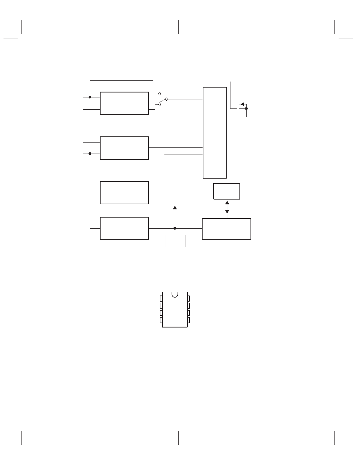
1.2 Functional Block Diagram
IN
CEX
OSCR
OSCC
7
6
1
2
Amplifier
Oscillator
Power-On
Reset
Test Mode
and
High Voltage
Interface
48
GND
V
CC
GND
Logic
Circuit
Shift
Register
EEPROM
Memory
5
OUT
3
TIME
1.3 Terminal Assignments
1–2
D OR P PACKAGE
(TOP VIEW)
OSCR
OSCC
TIME
GND
1
2
3
4
V
8
CC
IN
7
CEX
6
OUT
5

1.4 Terminal Functions
I/O
DESCRIPTION
TERMINAL
NAME NO.
CEX 6 I Capacitor external. CEX is used for gain control of the internal analog amplifier. An external
GND 4 Ground
IN 7 I/O Depending on the device configuration, IN provides inverted OUT data, is used as a receiver
OSCC 2 I/O Oscillator capacitor. Depending on the configuration, OSCC is used for external transmit/receive
OSCR 1 I Oscillator resistor. Depending on the configuration, OSCR is used as an external program/
OUT 5 O OUT is an open-drain output. For that reason, it is necessary to connect a pullup resistor to OUT.
capacitor connected from CEX to GND determines the gain of the amplifier. If the internal
amplifier is set for unity gain or the device is not used as a receiver, CEX is left unconnected.
input, or is used to enter data during programming.
– When the device is configured as a transmitter , IN provides the complement of the OUT
data stream and is considered to be noninverted. IN provides its own internal pullup, so
no external pullup is required when IN is used to transmit the data. It is cleared to 0 in
standby.
– When the device is configured as a receiver , IN is used to receive the code.
– When the device is in the program mode, IN is used to enter serial data into the device
shift registers that load into the EEPROM memory.
clock input, control of the internal oscillator, to place the device into program mode, input for a
high-voltage EEPROM programming pulse, or the internal analog amplifier in the test mode.
– When the device is used as a transmitter or receiver using an external clock, the external
clock is connected directly to OSCC. (OSCR must be held low to use an external clock.)
– When the device is used as a transmitter or receiver and the internal oscillator is used,
a capacitor from OSCC to GND and a resistor from OSCR to GND determines the
free-running internal oscillator frequency. In addition, the internal oscillator triangular
waveform can be seen at OSCC in this configuration.
– When the device is in the data-loading phase of the programming mode, OSCC must be
held at VCC + 0.5 V.
– After the device has been loaded with data in the programming mode, the internal
registers transfer the data to the EEPROM permanently by applying a high-voltage
programming pulse to OSCC.
– When OSCC is held at VCC + 0.5 V and three or more low pulses are applied to OSCR,
the device is in the test mode and the output of the internal analog amplifier can be
measured at TIME.
read clock input or to control the internal clock frequency.
– When the device is in the program/read mode, OSCR is connected to an external clock.
– When the device is in the transmit or receive mode, a resistor connected from OSCR to
GND (along with a capacitor from OSCC to GND) determines the frequency of the internal
clock.
Depending on the configuration, OUT provides transmit data, acts as the output for the receiver,
or provides the serial output of the stored data in memory during the program and read modes.
– When the device is configured as a transmitter, the transmitted data is seen at OUT and
is in a 3-state output mode during standby (OUT is floating). While transmitting, the data
from OUT is considered inverted.
– When the device is configured as a valid transmission receiver (VTR) receiver, OUT
provides a VTR pulse and goes low in the standby mode.
– When the device is configured as a Q-state receiver , OUT toggles high and low each time
a valid code is received.
– During the program mode, OUT provides the current data from the EEPROM memory
when the new data is clocked into the device.
1–3

1.4 Terminal Functions (Continued)
I/O
DESCRIPTION
TERMINAL
NAME NO.
TIME 3 I/O Depending on the configuration, TIME is used for measuring the internal analog-amplifier output
V
CC
8 5-V supply voltage
in the device test mode, putting the device into the transmit mode, or controlling an internal clock
oscillator for various transmitter and receiver configurations.
– When OSCC is held at VCC + 0.5 V and three or more low pulses are applied to OSCR,
the device is in the test mode and the output of the internal analog amplifier can be
measured at TIME.
– When the device is configured as a continuous transmitter , an internal pullup is connected
to TIME. If TIME is then forced low, the device transmits codes for the duration that TIME
is held low. (TIME must be connected to an external pullup.)
– When the device is configured as a triggered transmitter and if TIME is then forced low,
the device transmits one code or a code train. (TIME must be connected to an external
pullup.)
– When the device is configured as a periodic transmitter , connect an external resistor and
capacitor between TIME and VCC to transmit code after each RC time constant has
expired.
– When the device is configured as a VTR, TIME must be held high to receive codes. The
device produces a VTR pulse on OUT after confirmation of a correct received code.
Connecting a parallel resistor and capacitor between TIME and VCC lengthens the output
pulse (VTR) duration.
– Configured as a train receiver, connect an external parallel resistor and capacitor between
TIME and VCC, which are used to set the length of time the device is looking for two, four,
or eight correct received codes to output a valid VTR pulse on OUT.
– Configured as a Q-state receiver , TIME has the same function as the VTR receiver above,
except the detection of the correct code causes OUT to toggle between the low and high
states.
1–4

2 Specifications
2.1 Absolute Maximum Ratings Over Operating Free-Air Temperature Range
(Unless Otherwise Noted)
Supply voltage range, VCC (see Note 1) –0.6 V to 7 V. . . . . . . . . . . . . . . . . . . . . . . . . . . .
Input voltage range (except OSCC), V
Input voltage range, OSCC, V
Output voltage range, OUT, V
Operating free-air temperature range, T
Storage temperature range, T
†
Stresses beyond those listed under “absolute maximum ratings” may cause permanent damage to the device. These
are stress ratings only, and functional operation of the device at these or any other conditions beyond those indicated
under “recommended operating conditions” is not implied. Exposure to absolute-maximum-rated conditions for
extended periods may affect device reliability.
NOTE 1: Voltage values are with respect to GND.
2.2 Recommended Operating Conditions
Supply voltage, V
High-level input voltage, V
Low-level input voltage, V
Operating free-air temperature, T
Receiver supply current, analog, I
Receiver supply current, digital, I
Transmitter supply current, standby, I
Transmitter supply current, code transmission,
I
CC(code)
Programming current at OSCC, I
Oscillating period, tp0+ tp1 (see Figure 3–1) 10 1/(f
Pulse duration, logic 1 bit, tw1 (see Figure 3–1) 5 t
Pulse duration, logic 0 bit, tw2 (see Figure 3–1) 35 3 x tp0 + 4 x t
Setup time, transmitter/receiver external clock on
OSCC↓ and before IN↑, t
Pulse duration, IN high, tw3 (see Figure 3–2) 48
NOTES: 2. R
CC
IH
IL
A
CC(an)
CC(dig)
OSCC
(see Figure 3–2)
su1
is the value of the pullup resistor on TIME and C
TIME
R
. C
TIME
should not exceed 3 µF.
TIME
†
–0.6 V to V
–0.6 V to 15 V. . . . . . . . . . . . . . . . . . . . . . . . . . . . . . . . . . . .
I
–0.6 V to 15 V. . . . . . . . . . . . . . . . . . . . . . . . . . . . . . . . . . .
O
stg
CC(stdby)
I
–25°C to 85°C. . . . . . . . . . . . . . . . . . . . . . . . . .
A
–65°C to 150°C. . . . . . . . . . . . . . . . . . . . . . . . . . . . . . . . .
MIN NOM MAX UNIT
3 6 V
VCC–0.5 V
0 0.5 V
–25 85 °C
) 200 µs
osc
p1
19 × t
152
TIME
w1
(receiver)
6 × t
w1
(receiver)
is the value of the capacitor in parallel with
p1
CC
2 mA
200 µA
13 µA
260 µA
100 µA
100 µs
700 µs
R
× C
TIME
(see Note 2)
CC
TIME
+ 0.5 V. . . . . . . . . . . . . . . . . . . . .
V
µs
µs
2–1
2.3 Electrical Characteristics Over Recommended Ranges of Supply Voltage
V
V
V
V
AVFlatband gain
V/V
and Operating Free-Air Temperature (unless otherwise noted)
2.3.1 Signal Interface
PARAMETER TEST CONDITIONS MIN TYP MAX UNIT
OL
OH
I
I
I
O
C
i
C
o
2.3.2 Amplifier
V
I(PP)
V
N(PP)
V
O
B Bandwidth
Low-level output voltage, OUT IOL < 5 mA 0.5
Low-level output voltage, OSCC 0.6 0.7
High-level output voltage, OUT IOH < 5 mA VCC–0.5
High-level output voltage, OSCC 1.2 1.6
Input current, IN VI = 0 V to 6 V ±10 µA
Output current, OUT VO = 0 V to 12 V ±10 µA
Input capacitance 10 pF
Output capacitance 5 pF
PARAMETER TEST CONDITIONS MIN TYP MAX UNIT
Peak-to-peak input voltage 3 mV
External peak-to-peak noise voltage 1 mV
Output voltage, TIME V
VI = 3 mV 15
VI = 100 mV
VI = 200 mV
CEX (nF) > 900/f
CEX not connected 1
peak to peak
peak to peak
(kHz) 200
osc
OL
V
OH
500
1000
V
kHz
2.3.3 Internal Oscillator (see Note 3)
PARAMETER MIN TYP MAX UNIT
f
Receiver frequency 10 500 kHz
RX
f
Transmitter frequency fRX/10 fRX/10 fRX/5.5 kHz
TX
Frequency spread (temperature, VCC) ± 20%
NOTE 3: Typical values are recommended whenever possible.
2.3.4 Power-On Reset
PARAMETER MIN MAX UNIT
VCC level required to trigger power-on reset 2.7 V
Power-on reset duration 40 ms
2.3.5 Write/Erase Endurance
PARAMETER MIN TYP MAX UNIT
Number of program cycles 20 10000
2–2
2.4 Timing Requirements Over Recommended Ranges of Supply Voltages
and Free-Air Temperature
2.4.1 Abort/Retry
MIN NOM MAX
Time between consecutive codes 46 x tw (transmitter)
Time out for high-level bit to abort the code 3 x tw (receiver)
Time out for low-level bit to abort the code 25 x tw (receiver)
Time between aborted code and reading of new code 3 x tw (receiver)
2.4.2 EEPROM Read Mode (see Figure 3–3)
MIN MAX UNIT
t
Setup time, OSCR high after VCC ↑ 50 ms
su2
t
Pulse width, OSCR high 10 µs
w4
t
Pulse width, OSCR low 10 µs
w5
2.4.3 EEPROM Write Mode (see Figure 3–3 and Figure 3–4)
MIN MAX UNIT
t
Setup time, OSCR high after VCC high 50 ms
su3
t
Pulse duration, OSCR high 5 µs
w6
t
Pulse duration, OSCR low 5 µs
w7
t
Valid time, data IN valid before OSCC↑ 10 µs
v
2.4.4 Data Input Setup and Hold Times (see Figure 3–5)
MIN NOM MAX UNIT
t
Setup time, data in before OSCR↓ 1 µs
su4
t
Hold time, data in after OSCR↓ 1 µs
h1
2.5 Switching Characteristics Over Recommended Ranges of Supply
Voltages and Free-Air Temperature (unless otherwise noted)
2.5.1 Normal Transmission – Internal Clock (see Figure 3–6)
PARAMETER MIN TYP MAX UNIT
t
Pulse duration, half-oscillating period for OSCC sawtooth ↑↓ 5 1/(2 x f
w8
t
Pulse duration, logic bit 1 for IN 5 t
w9
t
Pulse duration, logic bit 0 for IN 35 7 x t
w10
2.5.2 Modulated Transmission – Internal Clock
f
osc(t)
f
osc(r)
t
w(H)
t
c
t
c(total)
t
w11
t
w12
PARAMETER
Transmitter oscillator frequency 100 110 120 kHz
Receiver oscillator frequency 400 440 480 kHz
Pulse duration, high-level modulation at IN See Figure 3-7 9 1/f
Cycle time, IN See Figure 3-7 27 3 x t
Total cycle time, IN See Figure 3-7 135 5 x t
Pulse duration, logic bit 1 for IN See Figure 3-7 135 5 x t
Pulse duration, logic bit 0 for IN See Figure 3-7 945 7 x t
CONDITIOINS
TEST
MIN TYP MAX UNIT
) 100 µs
osc
w
w
osc(t)
w(H)
c
c
1050 µs
w10
150 µs
150 µs
100 µs
700 µs
10 µs
30 µs
2–3

2–4
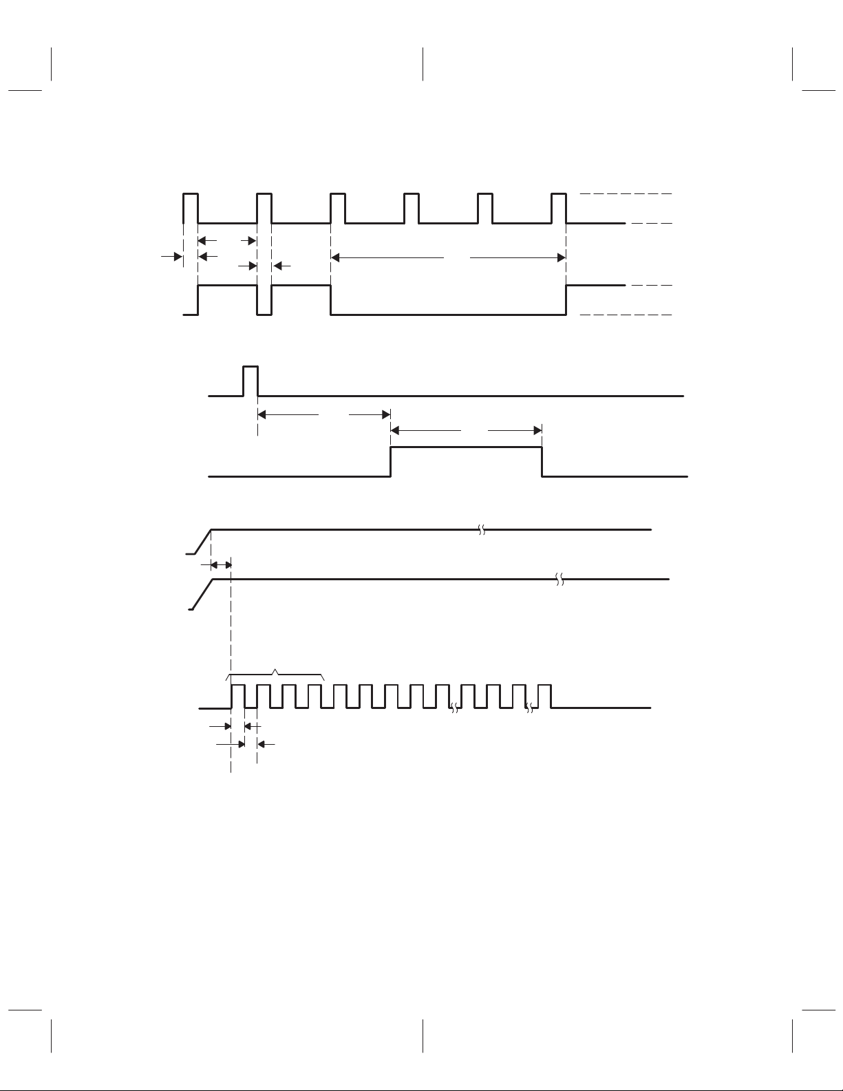
3 Parameter Measurement Information
OSCC
t
p0
t
p1
IN
OSCC
IN
t
w1
Figure 3–1. Normal Transmission – External Clock
t
su1
Figure 3–2. VTR Generation
V
IH
V
IL
t
w2
V
IH
V
IL
t
w3
V
CC
t
OSCC
OSCR
(clock in)
5 V
su2
t
w4
t
5 V
5.5 V
4 Reset Pulses
w5
Figure 3–3. EEPROM Read Mode
3–1
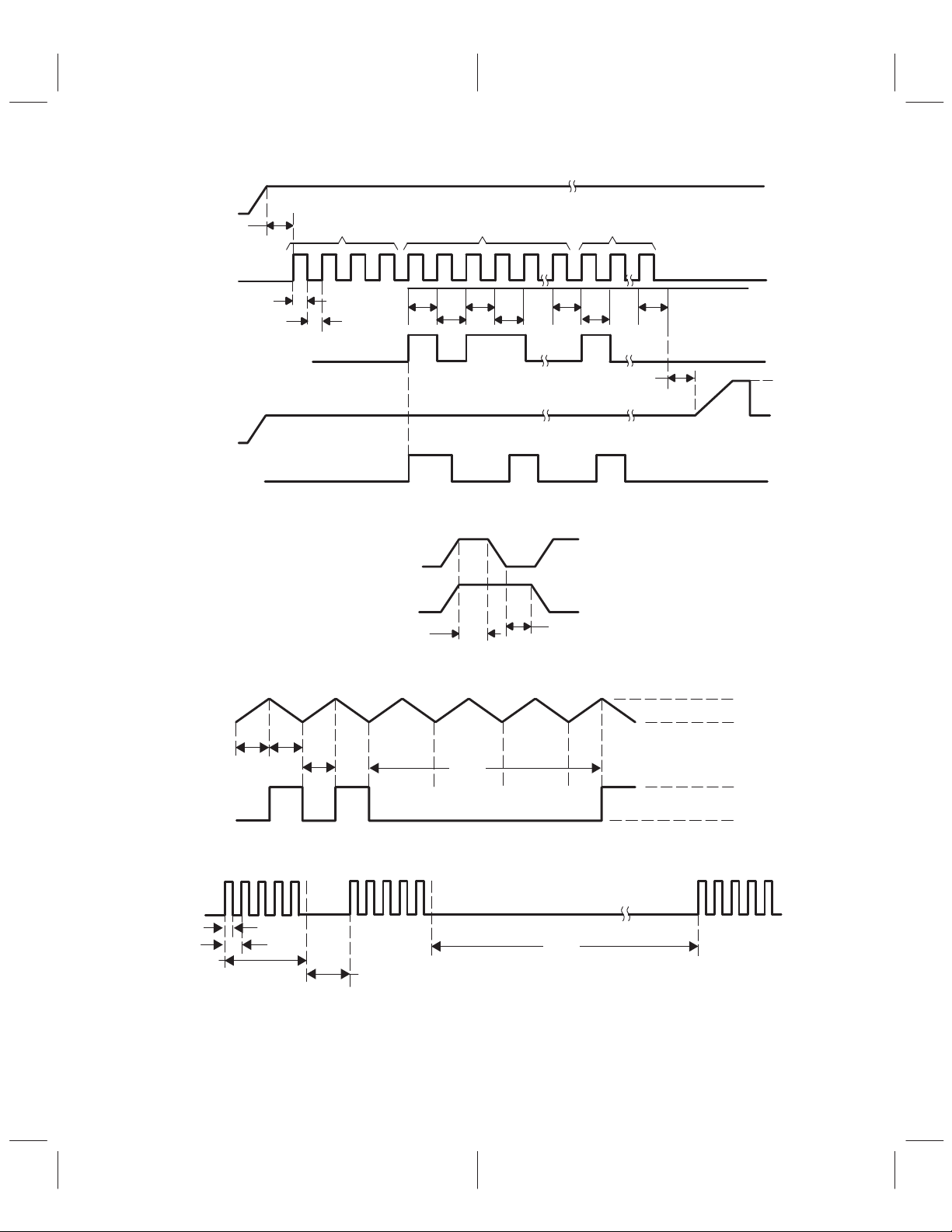
V
V
V
CC
OSCR
(clock in)
(data in)
t
IN
su3
5 V
5 V
4 Reset Pulses 22 Security Bits
t
w6
t
w7
C01–C22 CA–CI
C01
C02
C03
C04
9 Configuration Bits
C22
CA
t
v
CI
15
OSCC
(previous data)
OUT
OSCC
IN
tw8t
Figure 3–4. EEPROM Write Mode
OSCR
(clock)
IN
(data in)
t
su4
Figure 3–5. Data In Setup and Hold Times
w8
t
w9
t
w10
Figure 3–6. Normal Transmission – Internal Clock
High-Voltage
Programming Pulse
t
h1
5.5
V
IH
V
IL
V
IH
V
IL
tc
3–2
t
w(H)
(total)
IN
t
c
t
w11
t
w12
Figure 3–7. Modulated Transmission – Internal Clock

4 Typical Characteristics
8
7
6
5
4
3
– Supply Voltage – V
2
CC
V
1
0
0
22 kΩ
10 50 100
R
– Oscillator Resistance – kΩ
osc
Figure 4–1. Oscillator Resistance Versus Supply Voltage
7
10
R
6
10
10
5
R
R
osc
osc
osc
200
= 100 kΩ
= 47 kΩ
= 22 kΩ
220 kΩ
300
4
10
3
10
– Oscillator Frequency – Hz
2
osc
10
f
1
10
10
10 100 1000 10000 100000 1000000
C
– Oscillator Capacitance – pF
osc
Figure 4–2. Oscillator Frequency Versus Oscillator Capacitance
4–1

15
10
15 V
5
– Input Voltage at OSCC – V
I
V
0
0
> 3 ms
510151613 1411 121234 6789
t – Time – ms
>1 ms
Figure 4–3. High-Voltage Programming Pulse
5.5 V
4–2

5 Principles of Operation
5.1 Power-On Reset
The power-on reset function starts when VCC rises above 2.7 V and is completed after four clock periods.
After power-on reset, the nine configuration bits contained in the EEPROM memory are loaded into the logic
circuits, which determine the device mode and configuration of operation. For correct enabling of the
power-on reset operation, it is necessary for V
least 0.5 ms.
5.2 EEPROM Memory (31 Bits)
The EEPROM memory contains a total of 31 bits. The first 22 of the 31 bits contain the security code. These
22 bits are named C01, C02,...C22, and are user definable. The last 9 bits of the total 31 bits are
configuration bits named CA,CB,...CI, and are also user definable to select the mode of operation for the
device.
5.2.1 Program Read Mode
The procedure described in the following steps is used to read the current contents of the EEPROM memory .
This can verify that the correct 22 security codes and 9 configuration bits are stored in memory (see
Figure 5–1):
1. Set V
2. Apply V
(t
are in the following configuration:
• OSCR: program/read external clock input
• OUT: serial output of 31 data bits currently stored in EEPROM
3. Apply four reset pulses to OSCR (t
read operation.
to 5 V.
CC
+ 0.5 V to OSCC. Wait at least 50 ms to allow the device to assume the read mode
CC
> 50 ms). This voltage on OSCC forces the device into the read mode, and the terminals
su2
to first fall below 2.3 V and remain in this condition for at
CC
= tw5 = 10 µs). This only needs to be done once during each
w4
4. Apply 31 clock pulses to clock input OSCR (t
= tw5 = 10 µs min). This clocks out the 31 data
w4
bits (C01,C02,...C22, and CA,CB,...CI) that are stored in memory. Output data changes state
only on falling edge of clock pulses, except on data bit C01. If used, data bit C01 goes high on
the rising edge of the clock pulse.
NOTE:
Each succeeding group of 31 clock pulses, when applied, clocks out the data again
without any reset pulses required.
5–1

V
CC
OSCR
(clock in)
OUT
t
su2
4 Reset Pulses
t
w4
t
w5
C01
C01–C22
22 Security Bits
C03
C02
C04
CA–C1
9 Configuration Bits
C22
CA
5 V
CI
OSCC
5.5 V
Figure 5–1. EEPROM Read Mode
5.2.2 Program Write Mode
The procedure to write the 31 security code and configuration bits to memory is described below (see
Section 3 for timing diagram):
1. Set V
2. Apply V
and the terminals are in the following configuration:
• OSCR: program/read external clock input
• OSCC: input for high-voltage programming pulse used to permanently store data in memory
• OUT: serial output of 31 data bits currently stored in EEPROM
• IN: serial input for 31 bits of data to be stored
3. After applying V
program mode.
4. Apply exactly four clock reset pulses to OSCR (clock input). These reset pulses are applied
before clock input pulses for the 31 data bits that contain the security code and configuration bits.
The minimum duration of the clock reset pulses must be t
clock frequency <100 kHz.
5. Apply exactly 31 clock input pulses to OSCR. This serves to clock in the 31 data bits that should
be applied to IN (C01,C02,...C22, and CA,CB,...CI). Each of the 31 data bits must be present
on the falling edges of the clock input pulses applied to OSCR with the setup and hold times being
1 µs minimum.
6. The data at OUT is previous data that was stored in EEPROM before this operation. If the device
has never been programmed, this data is a random factory test code. The newly programmed
data can be read only after it is loaded.
7. Apply a logic low to OSCR for at least 10 µs.
to 5 V.
CC
+ 0.5 V to OSCC. This voltage on OSCC forces the device into the program mode,
CC
(see Figure 5–2).
+ 0.5 V to OSCC (step 2), wait at least 50 ms to allow device to go into the
CC
= tw7 = > 5 µs, which equates to a
w6
5–2

8. After a minimum valid time of t
= 10 µs, apply the high-voltage programming pulse to
v
permanently store the 31 code bits in EEPROM memory as shown in Figure 5–2. As stated in
steps 4 and 5, exactly 4 reset and 31 clock pulses must be applied for the device to successfully
program. The device does not transfer the code from its registers into the EEPROM if less than
or greater than 4 reset and 31 clock pulses are used before the programming pulse is applied.
5 V
V
CC
t
su3
OSCR
(clock in)
t
w6
t
IN
(data in)
OSCC
OUT
(previous data)
†
Previous data refers to data that was previously programmed into the device. If programmed for first time, this contains
†
4 Reset Pulses 22 Security Bits
C01
w7
OSCR
(clock)
IN
(data in)
t
> 1 µs
su4
C01–C22 CA–CI
C03
C02
C04
9 Configuration Bits
C22
th1 > 1 µs
CA
CI
t
v
High-Voltage
Programming Pulse
5 V
a random test code from the factory.
Figure 5–2. EEPROM Write Mode
15 V
5.5 V
5.3 Internal Oscillator Operation for Transmit and Receive Modes Setting
Frequency
The TMS3637 has an internal oscillator that can be used in either the transmit or receive configurations of
the device. The oscillator free-running frequency (f
and is determined by:
f
= 5 / (4 × C
osc
osc
× R
) (1)
osc
where
= capacitor from OSCC to GND
C
osc
R
= resistor from OSCR to GND
osc
The allowable oscillation range or R
three given values of R
are given in Section 4.
osc
versus VCC, and associated f
osc
) is controlled by an external resistor and capacitor
osc
values, and range versus C
osc
osc
for
5–3

5.4 Internal Oscillator Operation for Transmit and Receive Modes Sampling
Ǹ
Frequency
The internal oscillator of the transmitter or receiver can be externally sampled at OSCC and OSCR. The
waveform at OSCC is triangular and the waveform at OSCR is square. The amplitude of these waveforms
depends on the capacitor and resistor values used.
5.5 External Oscillator Operation for Transmit and Receive Modes
Instead of using the internal oscillator (with an external resistor and capacitor) in the transmit or receive
modes, it is possible to externally drive the device by applying a logic level clock to OSCC. When an
externally driven oscillator is used, OSCR must be held to GND. T o avoid entering the test/program modes,
ensure that the external clock applied to OSCC does not exceed V
Section 5.12).
(for more information see
CC
5.6 Internal Amplifier/Comparator, Description and Gain Setting
The TMS3637 has an internal amplifier that is designed to amplify received signals up to logic levels. In
addition, a comparator is cascaded with the amplifier to provide wave shaping of received signals. The
comparator also inverts the signal. The minimum received signal strength must be at least 3 mV
peak-to-peak (see Figure 5–3 for a schematic of the amplifier/comparator section). The amplifier is enabled
only when the TMS3637 is configured as an analog receiver. When the amplifier is not configured as an
analog receiver, it is disabled and bypassed to reduce power consumption in any of the three logic receiver
modes. A capacitor connected between CEX to GND determines the gain of the amplifier stage. When no
capacitor is connected from CEX to GND, the amplifier assumes unity gain and the comparator still functions
to shape the received signal. When the internal amplifier is used, it is usually run at the maximum gain of
200. The maximum gain is set by resistances internal to the device as shown in the equation 2. However ,
to achieve this maximum gain, a low impedance from CEX to GND must exist. Equation 2 defines the
capacitance necessary at CEX for maximum gain at different oscillator frequencies (f
CEX > 1 / (6.28 × f
where:
CEX = capacitance required for maximum gain
R1 = 178 Ω (set internally)
× R1) (2)
osc
osc
):
With a low impedance between GND and CEX, note that the maximum gain is derived from the noninverting
operational amplifier gain equation, (see Figure 5–3):
Gv = 1 + R2/R1 = 200 (3)
where:
R1 = 178 Ω (set internally)
R2 = 35.5 kΩ (set internally)
If a capacitor is used at CEX, but maximum gain is not desired, equation 4 can determine the gain for any
value of CEX:
Gv
+
where:
f
= oscillator frequency of transmitter (it is the transmitted frequency that is being amplified)
osc
C
= CEX + 0.15 nF (there is an internal capacitance of 0.15 nF at CEX)
T
R1 = 178 Ω (set internally)
R2 = 35.5 kΩ (set internally)
5–4
ǒ
1)4
p2f
1)4
2
CT2(R1)R2)
osc
2
p2f
osc
CT2R1
2
Ǔ
2
(4)

IN
(Ai)
R1
178 Ω
(internal)
+ +
CEX
Amplifier
+
–
R2
35.5 kΩ
(internal)
0.15 nF
(internal)
(Ao)
Comparator
200-mV Reference
+
_
(internal)
Figure 5–3. Amplifier/Comparator Schematic
5.7 Internal Amplifier/Comparator Test Mode
Normally, the output of the amplifier/comparator section is fed directly to the logic circuitry internal to the
device; however, the output of the amplifier/comparator can be sampled external to the device during the
amplifier test mode to determine if the amplitude and shape of the received signal is acceptable for the
application. T o enter the amplifier test mode, apply V
+0.5 V to OSCC and apply three or more low-level
CC
pulses to OSCR. This can be done by simply brushing a wire connected from OSCR to GND. The output
of the amplifier stage is then connected internally to TIME, where it can be sampled for evaluation purposes.
5.8 Mode and Configuration Overview
The TMS3637 device is designed to function in many modes and configurations. The device has five primary
modes of operation as shown in Table 5–1.
T able 5–1. Mode and Test Configuration
MODE DESCRIPTION
1 Amplifier Test
2 Program
3 Read
4 Transmitter
5 Receiver
In the transmitter and receiver modes (see Tables 5–2 and 5–3), there are a total of 66 configurations
available, 48 in the receiver mode and 18 in the transmitter mode.
5–5

NO. OF
(internal
GND
waveform
MODES
†
X = don’t care and can be held high or low
1
1
1
1
1
1
3
3
1
3
CONFIG.
Normal
Continuous
Normal
Triggered
Normal
Periodic
Modulated
Triggered
Modulated
Continuous
Modulated
Periodic
Code Train
Normal
Triggered
Code Train
Normal
Periodic
Code Train
Modulated
Triggered
Code Train
Modulated
Periodic
OSCR
(PIN 1)
External
clock or
resistor to
(internal
clock)
OSCC
(PIN 2)
Capacitor to
GND
clock) and
output of the
internal
clock
triangular
T able 5–2. Transmitter Modes
TIME
(PIN 3)
Starts
transmitting
when low stored data memory
OUT
(PIN 5)
Serial output
of currently
CEX
(PIN 6)IN(PIN 7)
N/C N/C
C1–C22
ABCDEFG
HI
Transmit
data from
CA–CI
ABCDEFG
†
HI
11100000X
110DE0001
110DE0000
100DE0001
10100000X
100000000
110DE0001
110DE0000
100DE0001
100DE0000
5–6

T able 5–3. Receiver Modes
ca acitor in
to GND
g
y
g
clock or
Ca acitor
lengthen
of currently
u
(Int
l
Wh
in ut
eriodic
l
V
CC
and
NO. OF
MODES
†
Number of modes refers to total possible modes for that configuration: includes noninverting or inverting and number
of codes (train).
‡
X = don’t care and can be held high or low, I = 1 inverting, I = 0 for noninverting
CONFIG.
†
Analog
Normal
2
VTR
Analog
Normal
6
Train
Analog
Normal
8
Q-state
Modulated
2
VTR
Modulated
6
Train
Modulated
8
Q-state
Logic
Normal
2
VTR
Logic
Normal
6
Train
Logic
Normal
8
Q-state
OSCR
(PIN 1)
External
clock or
resistor to
GND
erna
clock)
OSCC
(PIN 2)
p
to GND
(Internal
clock)
TIME
(PIN 3)
Requires a
high-toenable
receiver or
a resistor
and
p
parallel
connected
between
VCC and
ground to
nthn
l
the OUT
pulse.
en
operated in
periodic
mode, a
resistor and
capacitor in
paralle
connected
between
and
V
ground
causes a
reset.
OUT
(PIN 5)
Serial output
of currentl
stored data
and
configuration
data
CEX
(PIN 6)IN(PIN 7)
Capacitor
for
receiver
analo
amplifier
gain
N/C
Receive
signal
inp
C1–C22
ABCDEF
GHI
Data
received
t
CA–CI
ABCDEFG
HI
010XX010I
010DE01 1I
010DE000I
000XXX10I
000DEX1 1I
000DEX00I
010XX1 10I
010DE1 11I
010DE100I
‡
The multitude of transmit and receive configurations are discussed in subsection 5.10.3 and Section 5.12.
A reference for the quick, correct programming of the device in the desired mode and configuration is
discussed in Section 5.12. Table 5–4 lists the signals required to set the amplifier test, program, and read
modes.
T able 5–4. Amplifier Test, Program, and Read Modes
NO. OF
Test
MODES
†
1 Amplifier
CONFIG.
Test
EEPROM
MODE
Amplifier
Program 1 Program External
Read 1 Read
†
Number of modes refers to total possible modes for that configuration; which includes noninverting mode or inverting
mode and number of train codes.
‡
X = don’t care and can be held high or low
OSCR
(PIN 1)
3 or
more low
pulses
clock
External
clock
OSCC
(PIN 2)
VCC + 0.5 V Internal
VCC + 0.5 V
and high
voltage
programming
pulse (ramp
to 15 V)
VCC + 0.5 V N/C Serial
TIME
(PIN 3)
amplifier
out
N/C Serial
OUT
(PIN 5)
N/C Capacitor
out of
previous
data
out of
stored
data
CEX
(PIN 6)IN(PIN 7)
to GND
(for gain)
N/C New
N/C N/C Stored
Receive
signal
input
serial
data and
configu-
ration
input
C1–C22
ABCDE
FGHI
‡
X
Data
to be
stored
data
CA–CI
ABCDE
FGHI
‡
X
Configu-
ration
to be
stored
Stored
configu-
ration
5–7

5.9 Transmitter Configurations
Of the total 31 data bits that are stored by the TMS3637, the last nine (CA through CI) configure the device
in one of 18 possible transmitter configurations. The device can run continuous, triggered, or
periodic in transmission. In addition, each of these functions can have a single, pulse, or train output in both
normal and modulated configurations. (For a definition of which configuration bits to set for all possible 18
transmitter configurations, see subsection 5.10.3.) To enter any transmitter configuration, always start by
setting EEPROM bits CA = 1 and CF = CG = CH = 0.
When OUT transmits the code, the code is considered to be inverted. OUT also requires an external pullup
resistor. When IN transmits the code, the code is the complement of OUT and is considered noninverted.
An internal pullup resistor is connected to IN, so no external pullup is required when it transmits the code.
5.9.1 Continuous Transmitter (CC = 1)
When the device is configured as a transmitter (CA = 1, CF = CG = CH = 0) and the EEPROM bit CC is set
to 1, the chip is programmed to function as a continuous transmitter. In this condition, the TMS3637 serially
transmits the same code indefinitely. The transmit sequence is enabled by setting TIME to low. TIME is
externally connected to a pullup resistor, so a simple switch between TIME and GND can force TIME low.
The code transmission continues as long as TIME is kept low. When TIME returns to high, the transmission
of the code is completed and the transmitter is disabled. The oscillator is consequently inhibited, and the
power consumption is reduced to the standby value (13 µA). The time between two consecutive codes (tbc)
during the transmission is equal to 57 pulse durations (tbc = 57 t
transmitter must be operated in either the normal (CB = 1) or modulated (CB = 0) modes.
5.9.2 Triggered Transmitter (CC = 0, CI = 1)
When the chip is configured as a transmitter (CA = 1, CF = CG = CH = 0) and EEPROM bits CC and CI
low and high, respectively, the chip is programmed to work as a triggered transmitter. The TMS3637
transmits a single code or a code train when TIME is forced low, and then the device enters the standby
mode. In order to retransmit a code, TIME must be taken high (or opened) and then forced low again. The
triggered transmitter must be operated in either the normal (CB = 1) or modulated (CB = 0) modes.
, see Figure 3–6). The continuous
w8
5.9.3 Periodic Transmitter (CC = 0, CI = 0)
When the chip is configured as a transmitter (CA =1, CF = CG = CH = 0) and the EEPROM bits CC and CI
are cleared to 0, the chip is programmed to work as a periodic transmitter. In this case, the internal pullup
resistor on TIME is disconnected and TIME is externally connected to V
TMS3637 transmits one code or a code train and goes into the standby mode. After a time equal to one RC
time constant, the TMS3637 is enabled and transmits the code again. The TMS3637 then enters the standby
mode and repeats the process. During the code transmission, the external capacitor is loaded by V
During the standby mode, it is discharged through the resistor. The transmission cycle starts again when
the capacitor voltage falls below the trigger value of TIME. In this way, it is possible to obtain a very low
average value of I
periodic transmitter must be operated in either the normal (CB = 1) or modulated (CB = 0) modes.
. Typically , it is possible to obtain ICC = 1.5 µA at a transmission frequency of 2 Hz. The
CC
through a parallel RC. The
CC
CC
5.10 Transmitter Modes
In addition to the three transmitter configurations discussed previously, the TMS3637 transmitter can
operate in four modes: normal, continuous, triggered, and periodic. The following paragraphs describe the
configuration bit setting required to place the TMS3637 in each of the four modes.
5–8
.

5.10.1 Normal Mode (CB = 1)
When the chip is configured as a continuous transmitter (CA = 1, CF = CG = CH = 0, and CC = 1), as a
triggered transmitter (CA = 1, CF = CG = CH = 0, and CC = 0, CI = 1), or as a periodic transmitter
(CA = 1, CF = CG = CH = 0, and CC = 0, CI = 0), and EEPROM bit CB is set to 1, the TMS3637 operates
as a normal transmitter and emits the stored code on OUT (the open drain requires a pullup resistor). The
format for the code appearing on OUT is:
• Each code transmission consists of a 3-bit precode (010) or sync word followed by 22 data bits
(C1 through C22) stored in the EEPROM.
• A bit code 1 is represented high with a duration of t
a duration of t
= 7 t1.
2
An example of OUT is shown in Figure 5–4.
C01 C02 C03 C04
00010011 011011
OUT
t
2
t
1
, and a bit code 0 is represented high with
1
C22
Precode (3 bits)
Security Code (22 bits)
Figure 5–4. OUT Waveform in Normal Transmission
5.10.2 Modulated Mode (CB = 0)
When the chip is configured as a continuous transmitter (CA = 1, CF = CG = CH = 0, and CC = 1), as a
triggered transmitter (CA = 1, CF = CG = CH = 0, and CC = 0, CI = 1), or as a periodic transmitter (CA = 1,
CF = CG = CH = 0, and CC = 0, CI = 0), and EEPROM bit CB clears to 0, the device is programmed to
function as a modulated transmitter. The oscillator frequency must be 120 kHz.
In the modulated mode, a bit code 1 is represented high with a pulse width of t
represented by a high of t
a pulse train composed of five elementary pulses. The total duration of t
25 µs
= 7 t4 as in the normal mode, except that the bit codes are each separated by
0
t
3
Bit Code 1
t4 = 125 µs
= 125 µs as shown in Figure 5–5.
4
t0 = 7t
4
Bit Code 0
= t4. A bit code 0 is
3
Figure 5–5. OUT Waveform in Modulated Mode
5.10.3 Code-Train Mode (CD, CE)
When the chip is configured as a triggered transmitter (CA = 1, CF = CG = CH = 0, and CC = 0,
CI = 1) or as a periodic transmitter (CA = 1, CF = CG = CH = 0 and CC = 0, CI = 0), it can transmit
the stored code two, four, or eight times, depending on the values stored in bits CD and CE as shown
in Table 5–5 and Figure 5–6.
5–9

Continuous
CC = 1
T able 5–5. Code-Train Modes
CD CE TRAIN
1
0
1
CC = 0, CI = 1
0
1
1
2 codes
4 codes
8 codes
Transmitter
CA = 1, CF = CG = CH = 0
Triggered
CC = 0, CI = 0
Periodic
TRAIN CODES
CD CE
0
0
1
0
0
1
1
1
NO. OF
CODES
1
2
4
8
Normal
CB = 1
Modulated
CB = 0
1 Code
CD, CE
Normal
CB = 1
2 Codes
CD, CE
Modulated
CB = 0
4 Codes
CD, CE
8 Codes
CD, CE
1 Code
CD, CE
2 Codes
CD, CE
4 Codes
CD, CE
Normal
CB = 1
8 Codes
CD, CE
Modulated
CB = 0
Figure 5–6. Transmitter Configurations
5.11 Receiver Configurations
As with the transmitter configurations, the TMS3637 uses the last nine bits of the 31 data bits stored in
memory to program the device for a multitude of receiver configurations (48 possible configurations). The
configuration must match the transmitter when selecting the receiver configuration (see Table 5–6 to
determine compatible transmitter and receiver combinations). The definition of which configuration bits to
set for all the possible 48 receiver configurations is discussed in Section 5.12.
In the receive mode, the TMS3637 receives the transmitted code on IN and compares the code with the code
stored in memory . When the two codes are equal, a valid transmission pulse is sent to OUT . T o have reliable
reception of the transmitted code, the receiver clock frequency must be approximately seven times greater
than the clock frequency for the transmitter clock. To set any receiver configuration in the receiver mode,
always start by clearing the EEPROM bits CA = CC = 0.
5–10

T able 5–6. Transmitter/Receiver Compatibility
RCVR
ANALOG
XMITTER
Continuous
Triggered
Periodic
Modulated
Continuous
Modulated
Triggered
Modulated
Periodic
Code Train
Triggered
Code Train
Periodic
Code Train
Modulated
Triggered
Code Train
Modulated
Periodic
†
X denotes compatible transmitter/receiver combinations.
NORMAL
Normal
Normal
Normal
Normal
Normal
ANALOG
NORMAL
VTR
XXX
XXX
XXX
XXX
TRAIN
XX X X XX
ANALOG
NORMAL
Q-STATE
MODULATED
VTR
XXX
XXX
XXX
XXX
XXX
MODULATED
TRAIN
MODULATED
Q-STATE
†
LOGIC
NORMAL
VTR
XXX
XXX
XXX
XXX
LOGIC
NORMAL
TRAIN
LOGIC
NORMAL
Q-STATE
5.11.1 Valid Transmission Receiver (CG = 1, CH = 0)
When the TMS3637 is configured as a receiver (CA = CC = 0) and the configuration bits CG = 1 and
CH = 0, the device is configured as a valid transmission receiver. Bits CB, CF, and CI must also be set to
specify modulated or normal modes, analog or logic (for normal mode only), and noninverting or inverting
format of the output code. Other receiver modes are discussed in Section 5.12.
In the valid transmission receiver (VTR) configuration, an external pullup resistor is connected to TIME.
When the TMS3637 recognizes the received code as correct, it produces a high pulse (VTR pulse) on OUT .
The VTR output pulse duration is equal to 48 times the pulse duration of the received data and is produced
after a delay time equal to 152 × 2/f
from the end of the received code. If a capacitor is added in parallel
osc
to the pullup resistor on TIME, the VTR pulse duration on the output terminal can be increased according
to a quantity determined by the time constant of RC. By choosing a large capacitor value (no greater than
1 µF), it is possible to have a VTR output pulse duration of up to several seconds. When the VTR duration
is longer than the repetition period of received codes, the VTR has a duration as long as that of the correct
received code.
5.11.2 Train Receiver (CG = 1, CH = 1, CD, CE)
When the TMS3637 is configured as a receiver (CA = CC = 0) and EEPROM bits CG and CH are both set
to 1, the device is configured as a train receiver. Bits CB, CF, and CI must also be set to specify modulated
or normal modes, analog or logic (for normal mode only), and noninverting or inverting format.
In the train-receiver configuration, the device outputs a VTR pulse on OUT only after the reception of two,
four, or eight received codes that occur within one period of the train code counter oscillator. This feature
5–11

further increases the security of the device by not recognizing the correct received code until it is repeated
two, four, or eight times within a period of time specified by an external RC combination described in the
following paragraphs.
When the TMS3637 is configured as a train receiver, connect an external resistor and capacitor in parallel
between TIME and V
, which sets the length of time the device searches for two, four, or eight correct
CC
received codes. When the device receives two, four , or eight correct codes (not necessarily in succession)
within the time constant of the external RC network, a valid VTR pulse is placed on OUT at the conclusion
of the RC time constant.
The number of codes in the train required is determined by the setting of bits CD and CE as shown in
Table 5–7.
Table 5–7. Bits CD and CE in Train Receiver
CD CE TRAIN
1 0 2 codes
0 1 4 codes
1 1 8 codes
5.11.3 Q-State Receiver (CG = 0, CH = 0, CD, CE)
When the TMS3637 is configured as a receiver (CA = CC = 0) and EEPROM bits CG and CH are both
cleared to 0, the device is configured as a Q-state receiver. Bits CB, CF, and CI must also be set to specify
modulated or normal modes, analog or logic (for normal mode only), and noninverting or inverting format
of the output code.
The Q-state receiver is similar to a train receiver, except that when a train of one, two, four or eight codes
are recognized as valid, OUT toggles. After power-on reset, OUT is floating, since OUT is an open-drain
output. As with the train receiver, OUT can change value only after the RC time constant present on TIME.
Use Table 5–8 to determine the setting of bits CD and CE.
Table 5–8. Bits CD and CE in Q-State Receiver
CD CE TRAIN
0 0 1 code
1 0 2 codes
0 1 4 codes
1 1 8 codes
5.12 Receiver Modes
Figure 5–7 shows all possible receiver combinations. The bit values are also shown that determine the mode
of operation.
5–12

TRAIN CODES
CD CE
0
0
1
0
0
1
1
1
NO. OF
CODES
1
2
4
8
VTR Receiver
CG = 1, CH = 0
Receiver
CA = 0, CC = 0
Train Receiver
CG = 1, CH = 1
Q-State Receiver
CG = 0, CH = 0
Modulated
CB = 0
Noninverting
Normal
CB = 1
Analog
CF = 0
Modulated
Logic
CF = 1
2 Codes
CD,CE
CB = 0
Inverting
Normal
CB = 1
Analog
CF = 0
4 Codes
CD, CE
Logic
CF = 1
8 Codes
CD, CE
1 Code
CD, CE
2 Codes
CD, CE
4 Codes
CD, CE
Modulated
CB = 0
Analog
CF = 0
8 Codes
CD, CE
Normal
CB = 1
Logic
CF = 1
Figure 5–7. Receiver Configurations
5.12.1 Normal Mode (CB = 1)
The normal receiver function corresponds to a normal transmitter.
5.12.2 Modulated Mode (CB = 0)
The modulated receiver functions in a way that corresponds to a modulated transmitter. The oscillator
frequency of the receiver must be 480 kHz. The signal used as an input must be demodulated to the carrier
frequency of 40 kHz and then sent to IN.
5.12.3 Analog Mode (CF = 0)
In this configuration, the received code is sent directly to IN where it is amplified and passed through a
comparator to filter and square the received code waveform to logic levels. The phase of the output signal
of the internal amplifier section is reversed with respect to the input. The capacitor connected between CEX
and GND and the internal resistor of 178 Ω determines the cutoff frequency of the amplifier, which is in a
high-pass configuration.
5–13

5.12.4 Logic Mode (CF = 1)
In this configuration, the received code is at logic level. The analog amplifier and comparator connected
internally to IN is bypassed. This is typically the configuration used when the transmitter and receiver are
connected together by a hard line.
5.12.5 Noninverting Mode (CI = 0) or Inverting Mode (CI = 1)
The code input to IN is not inverted before passing to the logic circuitry . The following considerations must
be taken to determine if a noninverting or inverting receiver should be used:
• Transmitting from OUT on the transmitter is considered inverted.
• Transmitting from IN on the transmitter is considered noninverted.
• Using the logic mode on the receiver (CF = 1) does not invert the signal.
• Using the analog mode on the receiver (CF = 0) does invert the signal.
• Determine whether the signal path between the transmitter and receiver inverts the signal.
The code input to IN is internally inverted before passing to the logic circuitry .
NOTE:
Do not use the TMS3637 in the log inverting modes CA = 0, CC = 0, CF = 0, or
CI = 1. The amplifier sensitivity is degraded in these modes.
5–14

6 Application Information
6.1 General Applications
In this section an example schematic is shown for each of the four transmission media categories for which
the device can be configured. These schematics help to define the capabilities of the TMS3637. When
configured for infrared, one transmitter works for both normal and modulated modes. In addition, a
recommended programming station is shown. The schematics are:
• Direct-wired connection of transmitter/receiver
– Two wires
– Four wires
• Infrared coupling of transmitter/receiver
– Normal transmission mode
– Modulated transmission mode
• Radio frequency (RF) coupling of transmitter/receiver
• RF receiver and decoder
• Programming station used to program the TMS3637
–
6.2 Direct-Wire Connection of Transmitter and Receiver
The transmitter and receiver can be connected together by a direct two-wire or four-wire line. Both
configurations are described in the following paragraphs.
6.2.1 Two-Wire Direct Connection
Table 6–1 list the parts for the schematic of a two-wire direct connection of the transmitter and receiver
shown in Figure 6–1. Only two wires are required, primarily because the transmitted code is superimposed
on the source voltage delivered to the transmitter, and the transmitter uses its own internal oscillator. The
transmitter is configured as a normal continuous transmitter and the content of the configuration EEPROM
cells is:
CA CB CC CD CE CF CG CH CI
111000000
The device uses its internal oscillator to clock the data out (transmitter) and clock data in (receiver). The
oscillating frequency of the transmitter is approximately 5.7 kHz. With V
OUT (point A) is a square waveform between 0 V (internal connection to GND) and 5 V. At point B, the
maximum value is 5 V (when OUT is open) and the minimum value is 4.8 × 10K/(10K+220) = 4.892 V (when
OUT is at 0 V). The voltage swing is then 5 V–4.892 V = 108 mV. The voltage swing must not be much
greater than 100 mV because this is superimposed on the source voltage used to power the device. At point
C, the maximum value is V
through capacitor C2. At point D, R6 and C4 act as a low-pass filter (with a cutoff frequency of approximately
11 kHz) so that the code passes but higher frequency noise is suppressed. The receiver is configured as
an analog normal 1-code Q-state noninverting receiver and the content of the EEPROM cells is:
The receiver is used in the noninverting mode. Using OUT on the transmitter to transmit the code inverts
it, but the internal analog amplifier in the receiver (CF = 0) reinverts the signal. The signal path between the
transmitter and receiver does not invert the signal. The result is a signal that is noninverted at the internal
logic controller of the receiver, hence use CI = 0 for a noninverting receiver.
As required, the oscillating frequency of the receiver is about ten times greater than that of the 57 kHz
transmitter. This is easily set by keeping R
The signal on IN is internally amplified and the gain is calculated using equation 1:
1)39 32.5E6 103E-18 1.27E9
G
ǒ
+
Ǹ
1)39 32.5E6 103E-18 31.7E3
/2 = 2.5 V and the minimum value is 2.5 V–0.108 V = 2.4 V due to the coupling
CC
CA CB CC CD CE CF CG CH CI
010000000
constant but reducing C
osc
Ǔ
+
13
= 5 V, the transmitted code on
CC
to one-tenth of its original value.
osc
(1)
6–1

The input to the internal comparator has a voltage swing of approximately 1.4 V peak-to-peak (13 × 108 mV).
OUT on the receiver maintains the same status for approximately 0.5 s (1M × 470 nF).
Table 6–1. Two-Wire Direct Connection
DEVICE FUNCTION
U1 TMS3637 configured as a normal continuous logic transmitter
U2 TMS3637 configured as a analog normal Q-state noninverting receiver
R1 Pullup resistor on OUT, an open drain
R2 Resistor on OSCR that, in conjunction with C1, determines the internal oscillator frequency of U1.
R3 Resistor that provides current limiting and isolation between VCC and transmitter OUT swing.
R4 Upper portion of voltage divider used to bias receiver output
R5 Lower portion of voltage divider used to bias receiver output
R6 Resistor that is part of RC low-pass network on front end of U2 receiver
R7 Resistor on TIME that, along with C5, determines OUT pulse duration on U2.
R8 Resistor on OSCR that, in conjunction with C7, determines internal oscillator frequency on U2.
R9 Current-limiting resistor for LED indicator
C1 Capacitor on OSCC that, in conjunction with R2, determines internal oscillator frequency of U1.
C2 AC-coupling capacitor for output logic pulses from U1
C3 Power-supply bypass capacitor
C4 Capacitor that is part of RC low-pass network used on front-end of U2 receiver.
C5 Capacitor on TIME that, in conjunction with R7, determines OUT pulse duration on U2.
C6 Capacitor that sets gain of internal receive amplifier in U2.
C7 Capacitor on OSCC that, in conjunction with R8, determines internal oscillator frequency of U2.
D1 LED for indication of Q-state output toggling on and off
6–2

VCC and Code
C
V
B
R3
220 Ω
+
C3
47 µF
D1
C
R1
10 kΩ
8765
V
IN CEX OUT
CC
A
U1 (transmitter)
C2
OSCR OSCC TIME GND
1234 1234
R2
22 kΩ
C1
10 nF
0.1 nF
100 kΩ
GND
C
R5
R4
100 kΩ
R6
22 kΩ
D
C4
680 pF
R7
1 MΩ
C5
470 nF
8765
V
IN CEX OUT
CC
U2 (receiver)
OSCR OSCC TIME GND
R8
22 kΩ
C7
1 nF
C6
10 nF
R9
220 Ω
OUT
Figure 6–1. T wo-Wire Direct Connection
6.2.2 Four-Wire Direct Connection
T able 6–2 lists the parts for the schematic of a four-wire direct connection of the transmitter/receiver shown
in Figure 6–2. In this example, the V
The transmitter is configured as a normal continuous transmitter and the content of the configuration
EEPROM cells is:
CA CB CC CD CE CF CG CH CI
111000000
The transmitter uses its external oscillator to clock the data out. This external oscillator is a simple inverting
(NOT) gate that has a positive feedback loop through a resistor. The frequency of the oscillator is
approximately 26 kHz.
The receiver is configured as a logic normal (1-code) Q-state inverting receiver, and the content of the
EEPROM cells is:
CA CB CC CD CE CF CG CH CI
010001001
The receiver is used in the inverting mode. The code is considered to be inverted when using OUT on the
transmitter to transmit the code. The signal path between the transmitter and receiver does not invert the
signal; using the logic mode (CF = 1) also does not invert the signal. The result is a signal that is inverted
at the internal logic controller of the receiver; then use CI = 1, and an inverting receiver is used. (When IN
transmits the code, the signal is not inverted; then use CI = 0. An external pullup is not required when IN
is used in this manner).
As required, the oscillating frequency is approximately 260 kHz, which is a frequency approximately ten
times greater than that of the transmitter. This is provided by the internal oscillator in the receiver. OUT on
the receiver maintains the same status for approximately 0.5 seconds (1M × 470 nF). A typical application
is an electronic key as shown in Figure 6–3.
, code, clock, and GND are provided through four separate wires.
CC
6–3

Table 6–2. Four-Wire Direct Connection
DEVICE FUNCTION
U1 TMS3637 configured as a normal continuous logic transmitter
U2 TMS3637 configured as an analog normal (1-code) Q-state noninverting receiver
U3 Inverter (NOT gate) used as external clock
R1 Feedback resistor for U3
R2 Resistor on TIME that, in conjunction with C2, determines OUT pulse duration on U2.
R3 Resistor on OSCR that, in conjunction with C3, determines internal oscillator frequency of U2.
R4 Pullup resistor for transmitter OUT, which is an open-drain output
R5 Current-limiting resistor for D1
C1 Part of feedback circuit used to cause U3 to oscillate
C2 Capacitor on TIME that, in conjunction with R2, determines OUT pulse duration on U2.
C3 Capacitor on OSCC that, in conjunction with R3, determines internal oscillator frequency of U2.
D1 LED for indication of received code
V
CC
Code
8765
V
IN CEX OUT
CC
U1 (transmitter)
OSCR OSCC TIME GND
1234
Clock
GND
R4
100 kΩ
8765
V
CC
R2
1 MΩ
U3
74HC14
R1
1.8 kΩ
470 nF
C1
22 nF
C2
OSCR OSCC TIME GND
1234
R3
22 kΩ
Figure 6–2. Four-Wire Direct Connection
IN CEX OUT
U2 (receiver)
C3
220 pF
D1
V
CC
R5
220 Ω
OUT
6–4

V
IN CEX OUT
CC
U1 (transmitter)
OSCR OSCC TIMEGND
V
CC
CODE GND CLK
Figure 6–3. Four-Wire Direct Connection Key
6.3 Infrared Coupling of Transmitter/Receiver — Normal Transmission Mode
Table 6-3 lists the parts for the schematic of an infrared transmitter working in the normal transmission
configuration as shown in Figure 6–4. T able 6–4 lists the parts for the infrared receiver shown in Figure 6–5.
The transmitter is configured as a normal continuous transmitter, and the content of the configuration
EEPROM cells is:
CA CB CC CD CE CF CG CH CI
111000000
The transmitter uses its internal oscillator to clock the data out. The frequency of the oscillator is
approximately 26 kHz.
The receiver is configured as a logic normal (1-code) Q-state inverting receiver and the content of the
EEPROM cells is:
CA CB CC CD CE CF CG CH CI
010001001
The receiver is used in the inverting mode. The code is considered to be inverted when using OUT on the
transmitter to transmit the code. The signal path between the transmitter and receiver does not invert the
signal. Using the logic mode (CF = 1) also does not invert the signal. The result is a signal that is inverted
at the internal logic controller of the receiver, then use CI = 1 for an inverting receiver.
As required, the oscillating frequency of the receiver is 260 kHz, which is approximately ten times greater
than that of the transmitter. This is provided by the internal oscillator in the receiver. OUT on the receiver
maintains the same status for approximately 0.5 seconds (1M × 470 nF).
6–5

Table 6–3. Infrared Transmitter Component Functions (Normal Transmission Mode)
DEVICE FUNCTION
U1 TMS3637 configured as a normal continuous transmitter
R1 Resistor on OSCR that, in conjunction with C1, determines the internal oscillator frequency of U1.
R2 Current-limiting resistor for LED
R3 Current-limiting base-drive resistor for Q1
R4 Pullup resistor for OUT on U1 and bias for Q1
R5 Current-limiting collector resistor for Q1
R6 Pullup resistor for TIME
C1 Capacitor on OSCC that, in conjunction with R1, determines the internal oscillator frequency of U1.
C2 Power-supply bypass capacitor
D1 LED for visual indication of transmitted code
D2 Infrared LED used to transmit code
Q1 The pnp transistor that drives infrared LEDs
S1 S1 is closed for transmission.
V
CC
R6
10 kΩ
87 65
V
CC
IN CEX OUT
U1 (transmitter)
OSCR OSCC TIME GND
1234
R1
100 kΩ
C1
470 pF
R2
220 Ω
R4
10 kΩ
D1
R3
220 Ω
R6
10 kΩ
Figure 6–4. Infrared Transmitter
D2
R5
3.9 Ω
Q1
+
C2
100 µF
6–6

T able 6–4. Infrared Receiver Component Functions (Normal Transmission Mode)
DEVICE FUNCTION
U1 TMS3637 configured as a logic normal (1-code) Q-state inverting receiver
R1 Current-limiting resistor for IR transistor Q1
R2 Base-bias resistor for Q1
R3 Collector current-limiting resistor for Q2
R4 Collector current-limiting resistor for Q3
R5 Emitter current-limiter for Q3
R6 Resistor on TIME that, in conjunction with C3, determines OUT pulse duration on U1.
R7 Resistor on OSCR that, in conjunction with C4, determines internal oscillator frequency of U1.
R8 Current-limiting resistor for LED indicator
C1 AC-coupling capacitor that passes fluctuating voltage from phototransistor Q1
C2 Power-supply bypass capacitor
C3 Capacitor on TIME that, in conjunction with R6, determines OUT pulse duration on U1.
C4 Capacitor on OSCC that, in conjunction with R7, determines the internal oscillator frequency of U1.
C5 Capacitor that determines the gain of the internal analog receive amplifier on U1.
D1 LED indicator that toggles on/off when valid code is received
+
C2
R3
100 kΩ
47 µF
R4
10 kΩ
330 Ω
R8
V
CC
R1
330 Ω
R2
100 kΩ
C1
0.1 µF
Q1
NPN IR
Phototransistor
Q3
Q2
2N2222
2N2222
R5
2.7 kΩ
R6
1 MΩ
470 nF
C3
Figure 6–5. Infrared Receiver
8765
V
IN CEX OUT
CC
U2 (receiver)
OSCR OSCC TIME GND
1234
R7
100 kΩ
C4
47 pF
D1
OUT
6–7

6.4 Infrared Coupling of Transmitter/Receiver— Modulated Transmission
Mode
Table 6–5 lists the parts for the schematic of an infrared receiver working in the modulated continuous
configuration shown in Figure 6–6. This modulated receiver can be used with a normal infrared transmitter
(see Figure 6–4) provided that the following guide lines are observed.
The transmitter is configured as a modulated transmitter, and the content of the configuration EEPROM cells
is:
CA CB CC CD CE CF CG CH CI
101000000
The oscillating frequency of the transmitter must always be 120 kHz. This is accomplished by using a correct
combination of R
The receiver is cascaded with a TDA3048 (or equivalent) to process the received signal and demodulate
it. The receiver is configured as a modulated (1-code) Q-state inverting receiver, and the content of the
EEPROM cells is:
The receiver is used in the inverting mode. The code is considered to be inverted when using OUT on the
transmitter to transmit the code. The signal path between the transmitter and receiver does not invert the
signal; using the modulated mode (CB = 0) also does not invert the signal. The result is a signal that is
inverted at the internal logic controller of the receiver; then CI = 1 for an inverting receiver. The oscillating
frequency of the receiver is approximately 900 kHz. OUT on the receiver maintains the same status for
approximately 0.5 seconds (1M × 470 nF).
osc
and C
.
osc
CA CB CC CD CE CF CG CH CI
000000001
6–8

T able 6–5. Infrared Receiver Component Functions (Modulated Transmission Mode)
DEVICE FUNCTION
U1 Demodulator TDA3048 (or equivalent)
U2 TMS3637 configured as a normal logic (1-code) Q-state inverting receiver
R1 Current-limiting resistor for U1
R2 Resistor on TIME that, in conjunction with C2, determines OUT pulse duration on U2.
R3 Resistor on OSCR that, in conjunction with C3, determines the internal oscillator frequency of U2.
R4 Power-supply current-limiting resistor
C1 Power-supply filter capacitor
C2 Capacitor on TIME that, in conjunction with R2, determines OUT pulse duration on U2.
C3 Capacitor on OSCC that, in conjunction with R3, determines the internal oscillator frequency of U2.
Q1 Infrared phototransistor for received code
D2 Diode that is used to prevent back-EMF in L2 from sourcing current to OUT.
L2 Coil of relay R1
RY1 Relay, 12 V, SPDT
Q1
10 kΩ
10 kΩ
47 nF
47 nF
47 nF 47 nF
U1 (TDA3048)
22 nF
6.3 nF
1.5 nF
10 nH
V
CC
R4
R1
22 Ω
+
C1
100 µF
R2
1 MΩ
C2
470 nF
22 kΩ
10 Ω
8765
V
CC
U2 (receiver)
OSCR OSCC TIME GND
123 4
R2
12 V
D2
L2
IN CEX OUT
C7
1 nF
RY1
Figure 6–6. Infrared Modulated Receiver
6–9

6.5 Radio Frequency (RF) Coupling of Transmitter and Receiver
T able 6–6 lists the parts for the schematic of a radio frequency transmitter and receiver shown in Figure 6–7.
In Figure 6–7, the transmitter is configured as a normal continuous transmitter and the content of the
configuration of the EEPROM cells is:
CA CB CC CD CE CF CG CH CI
111000000
The oscillating frequency of the transmitter is about 5.7 kHz, and the transmitter code is pulse modulated.
T able 6–6. RF Transmitter Component Functions
DEVICE FUNCTION
U1 TMC3637 configured as a transmitter
R1 Resistor on OSCR that, in conjunction with C1, determines the internal oscillator frequency of U1.
R2 Base drive current-Limiting resistor for Q1
C1 Capacitor on OSCC that, in conjunction with R1, determines the internal oscillator frequency of U1.
C2 Capacitive part of LC tank circuit variable for frequency adjustment (2 pF – 10 pF)
C3 Power-supply bypass capacitor (to present low impedance to RF on V
L1 Inductive part of LC tank circuit-strip-line type
L2 RF choke presents high impedance to RF between the tank and VCC.
Q1 The npn RF transistor turns on the LC circuit.
C3
10 pF
CC)
L2
10 µH
V
CC
L1
8765
V
CC
OSCR OSCC TIME GND
R1
22 kΩ
IN CEX OUT
U1 (transmitter)
12 34
C1
100 pF
S1
R2
15 kΩ
C4
2.2 pF
C2
10 pF
Q1
Figure 6–7. Radio Frequency Transmitter
Inductance L2 is an RF choke, while L1 is a strip-line 0.1-µH inductance that is 1.5-mm wide and 3.5-cm
long. The frequency range of the transmitter (tunable by C2–10 pF) is approximately 165 MHz – 370 MHz.
A good RF transistor with an H
exceeding 500 MHz is recommended. No external antenna is required,
FE
provided the recommended antenna is used on the receiver as described in the following paragraphs.
6–10

IN is used for the data out. IN provides the complement of the data out in the transmitter configuration.
In Figure 6–8, the receiver is configured as an analog normal noninverting VTR receiver, and the content
of the EEPROM cells is:
CA CB CC CD CE CF CG CH CI
010000100
The receiver is used in the noninverting mode. Using IN on the transmitter to transmit the code is considered
noninverted, but the internal analog amplifier in the receiver (CF = 0) inverts the signal. The signal path
between the transmitter and receiver also inverts the signal. The result is a signal that is noninverted at the
internal logic controller of the receiver, then C1 = 0, a noninverting receiver.
The receiver can be tuned from approximately 200 MHz – 430 MHz using the trim capacitor C4. The antenna
used is a metal wire that is 12 inches long. Inductances L1 and L2 are in the range of 0.2 µH – 2 µH.
The oscillating frequency of the receiver is 57 kHz, which is approximately ten times that of the transmitter,
and the gain of the internal analog amplifier is approximately 200. OUT on the receiver maintains the same
status for approximately 0.5 second (1M × 470 nF)
.
6–11

6–12
C5
C7
C9
L4
C8
C4
RF Input
R1R2
C3
C1
L1
C2
R8
C20
R7
DOUT
C19
R6
TRIG
BBOUT
C18
V
CC
C21
47 nF
C22
100 nF
F1
L2
SAW
Filter
L3
C6
131415161718192021222324
TRIG
RFOUT2
LNA2T
RFIN2
AGND
RFOUT1
LNA1T
RFIN1
AGND
DOUT
BBOUT
DGND
U1 RF Receiver
TRF1400
CC
LPF
AGND
1234567 89101112
C10
RFIN3
C13
AV
C11 C12
C14
AGND
AV
CC
AV
CC
AGND
OFFSET
R3
AGND
OSCR
R4
R5
OSCC
C15
CC
DV
C16
Figure 6–8. TRF1400 RF Receiver and TMS3637 Decoder Circuit
C17
DV
CC
R10
1 MΩ
470 nF
C24
8765
VCCIN CEX OUT
U2 Decoder
TMS3637
OSCR OSCC TIME GND
123 4
R9
22 kΩ
C23
1 nF

6.6 RF Receiver and Decoder
Table 6–7 lists the parts for the schematic shown in Figure 6–8. Figure 6–8 shows a Texas Instruments
TRF1400 RF receiver and a Texas Instruments TMS3637 receiver connected as an RF receiver and
decoder combination. T able 6–7 lists the components that comprise this circuit. As with any RF design, the
successful integration of these two devices relies heavily on the board layout and the quality of the external
components. This circuit demonstrates performance of the TRF1400 and TMS3637 at 300 MHz. Specified
component tolerances and, where applicable, Q should be observed during the selection of parts.
A complete set of Gerber photoplotter files for the TRF1400 circuit board can be obtained from any TI Field
Sales Office.
T able 6–7. TRF1400 RF Receiver and TCM3637 Decoder Parts List (for 300 MHz operation)
DESIGNATORS
C1
C2
C3
C4
C5
C6
C7
C8
C9
C10
C11
C12
C13
C14
C15
C16
C17
C18
C19
C20
C21
C22
C23
C24
§
E1
§
E2
§
E3
S1–S2
†
‡
§
TI is a trademark of Texas Instruments Incorporated.
F1
Tantalum capacitors are rated at 6.3 Vdc minimum
SAW = surface acoustic wave
Not shown on schematic
DESCRIPTION
Capacitor
Capacitor
Capacitor
Capacitor
Capacitor
Capacitor
Capacitor
Capacitor
Capacitor
Capacitor
Capacitor
Capacitor
Capacitor
Capacitor, Tantalum
Capacitor
Capacitor, Tantalum
Capacitor
Capacitor
Capacitor
Capacitor
Capacitor
Capacitor
Capacitor
Capacitor
2-Pin Connector
2-Pin Connector
6-Pin Connector
Header shunts
SAW filter
‡
VALUE
4 pF
22 pF
22 pF
100 pF
5 pF
1.5 pF
100 pF
3 pF
18 pF
0.047 µF
2200 pF
2200 pF
0.022 µF
†
†
4.7 µF
220 pF, 5%
4.7 µF
2200 pF
0.022 µF
2200 pF
0.022 µF
47 µF
100 µF
1 nF
470 nF
RF1211
MANUFACTURER
Murata
Murata
Murata
Murata
Murata
Murata
Murata
Murata
Murata
Murata
Murata
Murata
Murata
Sprague
Murata
Sprague
Murata
Murata
Murata
Murata
3M
3M
3M
3M
RFM
MANUFACTURER P/N
GRM40C0G040C050V
GRM40C0G220J050BD
GRM40C0G220J050BD
GRM40C0G101J050BD
GRM40C0G050D050BD
GRM40C0G1R5C050BD
GRM40C0G101J050BD
GRM40C0G030C050BD
GRM40C0G180J050BD
GRM40X7R473K050
GRM40X7R222K050BD
GRM40X7R222K050BD
GRM40X7R223K050BL
293D475X9050D2T
GRM40C0G221J050BD
293D475X9050D2T
GRM40X7R222K050BD
GRM40X7R223K050BL
GRM40X7R222K050BD
GRM40X7R223K050BL
2340–61 11–TN
2340–61 11–TN
2340–61 11–TN
929952–10
RF1211
6–13

T able 6–7. TRF1400 RF Receiver and TCM3637 Decoder Parts List
(for 300 MHz operation) (continued)
DESIGNATORS
L1
L2
L3
L4
P1
R1
R2
R3
R4
R5
R6
R7
R8
R9
R10
U1
U2
DESCRIPTION
Inductor
Inductor
Inductor
Inductor
RF SMA Connector
Resistor
Resistor
Resistor
Resistor
Resistor
Resistor
Resistor
Resistor
Resistor
Resistor
RF Receiver
Decoder
VALUE
47 nH
82 nH
120 nH
39 nH
1200 Ω
1200 Ω
1M Ω
130 KΩ, 1%
0 Ω
1 KΩ
100 Ω
1 KΩ
27 kΩ
1M Ω
MANUFACTURER
Coilcraft
Coilcraft
Coilcraft
Coilcraft
Johnson
Texas Instruments
Texas Instruments
MANUFACTURER P/N
0805HS470TMBC
0805HS820TKBC
0805HS121TKBC
0805HS390TMBC
142–0701–201
TRF1400
TMS3637
6.7 Programming Station
A programming station schematic is shown in Figure 6–9. This station is made up of two major parts: 1)a
shift register/clock circuit that outputs exactly 35 bits serially (four reset pulses, 22 security bits, and 9
configuration bits), and 2) a transistor ramp generator that outputs the programming pulse required to store
data in the EEPROM. The following paragraphs detail the function of the circuit.
Before the momentary switch SW5 is pressed, the shift registers U9–U13 shift-load input is low so that they
are continually loading whatever code is present on the DIP switches SW1–SW4. In addition, the binary
counter U6 is in a clear state and its output is 00000000.
When momentary switch SW5 is pressed, the set-reset (S-R) latch on U1 acts as a debouncer and outputs
a logic level 1, which releases the clear on binary counter U6. It places a high on the shift input to the shift
registers
U9 – U13, allowing them to shift out the stored 35 bits as soon as a clock is applied to them. The output of
the S-R latch on U1 is also connected to the D input of the D flip-flop on U2. The D flip-flop is clocked by
the free-running 555 timer (U8) configured for astable operation on a 8-kHz clock. Therefore, on the next
rising edge of the U8 clock, the D flip-flop on U2 outputs a high signal. The output of the D flip-flop enables
the AND gate on U3 to pass the 8-kHz clock. The 8-kHz clock signal is routed to the dual 4-bit binary counters
(U6) that have had their CLR terminal released by the S-R latch (from pressing the momentary switch SW5).
The outputs of the U6 counters are connected to the counter-comparator U7, which outputs low when the
count reaches exactly 35 clock pulses (as defined by the code 11000100 on U7 Q inputs). The output of U7
then clears the D flip-flop on U2, the 8-kHz clock is no longer able to pass, and the counting stops.
During this entire counting sequence, the shift registers U9 through U13 are clocked with exactly 35 bits.
Due to the momentary switch being pressed, the S-R latch output is high on the shift-register shift enable,
allowing the registers to shift out the 35 bits of data to the code input of the TMS3637. The TMS3637 is
clocked synchronously with this data on OSCR.
Because the binary counter U6 is released from its cleared state and the U9–U13 registers are allowed to
shift data only during the time that the momentary switch is pressed, it is required that the switch be held
6–14

closed for the duration of the entire clocking sequence which is 4.4 ms or greater
(125 µs × 35 bits = 4.4 ms).
At the conclusion of the count, the one-shot timer U5 is edge triggered by the output of the
counter-comparator U7. The output from U5 enables the EEPROM programming-pulse ramp generator that
is made up of Q1 and Q2. When U5 goes high (for approximately 13 ms), transistor Q1 turns on. U5 goes
high and turns off Q2, and the voltage on OSCC of the TMS3637 is allowed to ramp from 5.5 V to 17 V using
the RC time constant established by R10 and C5. The required ramp characteristics to successfully program
the EEPROM are defined in this data manual (see Figure 3–4). After the U5 time expires, the voltage on
OSCC again returns to 5.5 V (approximately one diode drop above 5 V) and the TMS3637 is programmed.
The U5 timer normally outputs one pulse when the circuit is powered up. This is inherent of the timer device.
To prevent the timer from outputting this pulse and inadvertently programming the TMS3637, a power-on
reset RC combination is included. When power is first applied to the circuit, timer U5 remains in the clear
state until capacitor C3 can charge through resistor R6, preventing the generation of a programming pulse.
After the programming button is released, the circuit again returns to its steady-state mode where counter
U6 is held in a cleared state and the shift resisters U9–U13 are always loaded with the current code on the
DIP switches SW1–SW4.
6–15

5 V
R1
Ω1 k
(B8)
SW5
SPST Momentary
Push to Program
GND
(A1)
(B1)
(A6)
5 V
R3
Ω2.2 k
R4
Ω7.5 k
C1
0.01 µF
U4 B
74LS04
43
(B7)
C2
0.1 µF
15
14
12
11
10
6
5
3
2
1
TLC555I
TRIG
RSET
DSCH
THRES
CON
U1
74LS279
4S
4R
3S2
3S1
3R
2S
2R
1S2
1S1
1R
U8
OUT
QA
QB
QC
QD
R5
5 V
(A9), (B9)
4Q
13
74HC74
9
7
DQ
CK
4
PR
U2A
CLR
8 kHz
Q
Q
C6
1 µF
U3 A
74HC21
U4 A
C
R
EXT
C
EXT
A
B
CLR
EXT
U5
74LS123
/
Q
Q
5 V
SN74ALS04
C4
R6
Ω3.9 k
C3
0.22 µF
0.47 µF
R7
Ω75 k
Ω10 k
5 V
R12–R15 RN1
Ω10 k
C1C2C3C4C5C6C7C
SW1
†††
D C B A SER
INH
74HC165
U9
CLK
LD
EFG
†
Notch in lower left corner of dip switches. Up is open = 1, down is closed = 0. All the chips are bypassed with 0.1-mF (C7–C20) ceramic
H
IN
QH
QH
Ω10 k
8
UP
DN
HGFE
INH
CLK
LD
C1–C22 Security
Code (22 Bits)
C9C10C11C12C13C14C15C
SW2
D C B A SER
74HC164
U10
16
UP
DN
IN
HGFE
INH
QH QH
QH
LD
SW3
74HC165
CLK
RN2
CA–CI Conf.
Ω10 k
Code (9 Bits)
C17C18C19C20C21C22CAC
D C B A SER
U11
B
IN
QH
capacitors.
UP
DN
6–16
Figure 6–9. Programming Station

35
J1 IN: Prog
J1 OUT: Read
2Q
1Q
JP1
R8
2A
U6 B
74HC393
QA
A
QB
QC
QD
CLR
U6 A
74HC393
QA
A
CLR
QB
QC
QD
5 V
17 V
R9
Ω9.1 k
Ω6.2 k
Q2
2N2222
Q1
2N2222
IN414B
D1
R10
CR1
Ω8.2 k
C5
0.1 µF
ΩR21, 10 k
ΩR20, 10 k
ΩR19, 10 k
74HC682
2
P0
4
P1
6
P2
8
P3
11
P4
13
P5
15
P6
17
P7
3
1
Q0
5
1
Q1
7
0
Q2
9
0
Q3
12
0
Q4
14
1
Q5
16
0
Q6
18
0
Q7
P = Q
P > Q
U7
19
1
5 V
RN3
Ω10 k
CCCDCECFCGCHC
SW4
†
HGFE
INH
74HC165
CLK
DCBASER
U12
IN
QH
QH
HGFE
INH
LD
†
Notch in lower left corner of dip switches. Up is open = 1, down is closed = 0. All the chips are bypassed with 0.1-mF (C7–C20) ceramic
LD
I Unused
74HC165
CLK
R16–R18
Ω10 k
UP
DN
D C B A SER
U13
IN
QH
QH
OSCC
1
2
3
4
OSCR
OSCC
TIME
V
CEX
V
OUT
SS
TMC3637
CC
IN
8
7
6
5
capacitors.
Figure 6–9. Programming Station (continued)
R11
Ω1 k
6–17

6.8 TMS3637 Programming Station Parts Lists
T able 6–8 contains a listing of the parts that compose the TMS3637 programming stations (see Figure 6–9
for a schematic).
T able 6–8. TMS3637 Programming Station Parts List
PART DESCRIPTION FUNCTION
R1 Resistor, 1 kΩ,, 1/4 watt R1 is an isolation resistor
R2 Resistor, 1 kΩ,, 1/4 watt With C1 and R4, R2 sets U8 discharge time
R4 Resistor, 1 kΩ,, 1/4 watt With C1, R2 sets U8 threshold level
R5 Resistor, 1 kΩ,, 1/4 watt R5 is the output pullup resistor for U8
R6 Resistor, 1 kΩ,, 1/4 watt With C3, R6 sets time constant for U5 CLR
R7 Resistor, 1 kΩ,, 1/4 watt With C4, R7 sets time constant for U5 CERT
R8 Resistor, 1 kΩ,, 1/4 watt R8 couples U5 dc output to base of Q2
R9 Resistor, 1 kΩ,, 1/4 watt R9 is the load resistor for Q2
R10 Resistor, 1 kΩ,, 1/4 watt With C5, R10 sets programming pulse ramp time
R11 Resistor, 1 kΩ,, 1/4 watt R11 is the output pullup resistor for U14
R12–R21 Resistor, 1 kΩ,, 1/4 watt R12–R21 are load resistors for the shift register
RN1–RN3 Resistor, 10 kΩ,, 1/4-watt 16-Pin DIP RN1–RN3 are Load resistors for the shift
C1 Ceramic Capacitor, 0.01-µF With R4, C1 sets U8 threshold level
C2 Ceramic Capacitor, 0.1-µF C2 sets control voltage level on U8
C3 Electrolytic Capacitor, 0.22-µF With R6, C3 prevents generation of program
C4 Electrolytic Capacitor, 0.47-µF With R7, C4 sets time constant for U5 CEXT
C5 Ceramic Capacitor, 0.1-µ F C5 couples high voltage programming pulse to
C6 Electrolytic Capacitor, 1-µF C6 is +5-V supply filter capacitor
C7–C19 Ceramic Capacitor, 0.01-µF C7–C15 are bypass capacitors
U1 TI SN74LS279 Quadruple S-R Latches The U1 latch acts as debouncer during reset
U2 TI SN74HC74 Dual D-Type
Positive-Edge-Triggered
Flip-Flops with Clear and Preset
U3 TI SN74HC21 Dual 4-Input Positive-AND Gates U3 is an 8-kHz gate to shift register and to U6
U4 TI SN7404 Hex Inverters U4 is a buffer and inverter
U5 TI SN74LS123 Retriggerable Monostable
Multivibrators
U6 TI SN47HC393 Dual 4-Bit Binary Counters U6 is a dual binary 4-bit sequential counter
U7 TI SN74HC682 8-Bit Magnitude Counter
Comparators
U8 TI TLC555I Astable/Monostable T imer U8 is a free-running timer (astable at 8 kHz)
U9–U13 TI SN74HC165 Parallel-Load 8-Bit Shift Registers U3–U13 shift programming data into the
terminal
terminal
data input
register data
pulse during initial power up
terminal
OSCC
U2 enables U3 to pass the 8-kHz clock
U5 is a one-shot timer; its output enables
EEPROM programming pulse from Q1 and Q2
U7 outputs low when the count reaches 35 clock
pulses as set by Q inputs
TMS3637
6–18

T able 6–8 TMS3637 Programming Station Parts List (continued)
PART DESCRIPTION FUNCTION
U14 TMC3637 Remote Control
Transmitter/Receiver
Q1, Q2 TI 2N2222 npn Transistor Q1 and Q2 are emitter followers that output the
CR1 1N4148 Silicon Diode CR1 is a blocking diode when an external
SW1–SW4 16-Pin DIP switch SW1–SW4 select input coding
SW5 SPST Momentary Switch SW5 when closed resets the device
U14 transmits or receives specific
user-configuration code
programming pulse
oscillator is used
6.9 TMS3637 Connector Pinout
TI recommends a ZIF socket to be used at location U14 for ease of programming the TMS3637. For
TMS3637P (DIP) packages, a 16-pin ZIF can be used (lower portion unused). For TMS3637N
surface-mount packages, use a clamshell with a latch cover and DIP footprint. This can be purchased from
EmMulation T echnology (408-982-0660) part # AS-0808-015-3. The edge connector that is compatible with
the TMS3637 PCB is a Sullins part # EZC10DRTH or the equivalent as shown in Table 6–9. Ground
terminals A1, A6, and B1 are common, so only one is needed for ground connection.
T able 6–9. Edge-Connector Pinout
EDGE CONNECTOR FUNCTION
A1 Ground
A2 N/C
A3 N/C
A4 N/C
A5 N/C
A6 Ground
A7 N/C
A8 N/C
A9 5 Vdc
A10 N/C
B1 Ground
B2 17 Vdc
B3 N/C
B4 N/C
B5 N/C
B6 N/C
B7 See Note 1
B8 See Note 1
B9 5 Vdc
B10 N/C (see Note 2)
NOTES: 1. Other edge connections are connected to various
parts of circuit. These are for testing purposes
only.
2. N/C = Not connected
6–19

6–20

IMPORTANT NOTICE
T exas Instruments and its subsidiaries (TI) reserve the right to make changes to their products or to discontinue
any product or service without notice, and advise customers to obtain the latest version of relevant information
to verify, before placing orders, that information being relied on is current and complete. All products are sold
subject to the terms and conditions of sale supplied at the time of order acknowledgement, including those
pertaining to warranty, patent infringement, and limitation of liability.
TI warrants performance of its semiconductor products to the specifications applicable at the time of sale in
accordance with TI’s standard warranty. Testing and other quality control techniques are utilized to the extent
TI deems necessary to support this warranty . Specific testing of all parameters of each device is not necessarily
performed, except those mandated by government requirements.
CERT AIN APPLICATIONS USING SEMICONDUCTOR PRODUCTS MAY INVOL VE POTENTIAL RISKS OF
DEATH, PERSONAL INJURY, OR SEVERE PROPERTY OR ENVIRONMENTAL DAMAGE (“CRITICAL
APPLICATIONS”). TI SEMICONDUCTOR PRODUCTS ARE NOT DESIGNED, AUTHORIZED, OR
WARRANTED TO BE SUITABLE FOR USE IN LIFE-SUPPORT DEVICES OR SYSTEMS OR OTHER
CRITICAL APPLICA TIONS. INCLUSION OF TI PRODUCTS IN SUCH APPLICATIONS IS UNDERST OOD TO
BE FULLY AT THE CUSTOMER’S RISK.
In order to minimize risks associated with the customer’s applications, adequate design and operating
safeguards must be provided by the customer to minimize inherent or procedural hazards.
TI assumes no liability for applications assistance or customer product design. TI does not warrant or represent
that any license, either express or implied, is granted under any patent right, copyright, mask work right, or other
intellectual property right of TI covering or relating to any combination, machine, or process in which such
semiconductor products or services might be or are used. TI’s publication of information regarding any third
party’s products or services does not constitute TI’s approval, warranty or endorsement thereof.
Copyright 1998, Texas Instruments Incorporated
 Loading...