

TMS3472A
SERIAL DRIVER
SOCS025B – FEBRUARY 1991
PD
SSR
V
SS
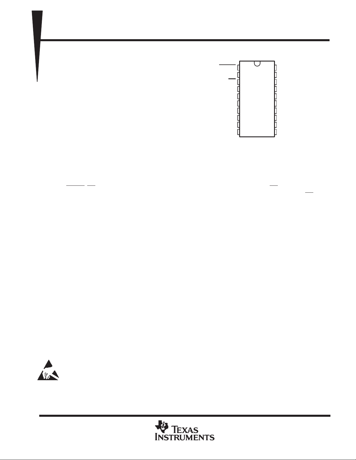
DW PACKAGE
(TOP VIEW)
1
2
3
4
5
6
7
8
9
10
20
19
18
17
16
15
14
13
12
11
V
SS
1PC2
1PC1
V
CC
SRG3OUT
SRG2OUT
SRG1OUT
TRGOUT
V
CC
TSR
• TTL-Compatible Inputs
• CCD-Compatible Outputs
• Variable-Output Slew Rates With External
Resistor Control
• Frame-Transfer Operation
• Solid-State Reliability
• Adjustable Clock Levels
description
The TMS3472A serial driver is a monolithic
CMOS integrated circuit designed to drive the
serial-register gate (SRGn) and transfer-gate
DLADJ
GND
SRG2,3IN
SRG1IN
TRGIN
2,3PC1
2,3PC2
(TRG) inputs of the Texas Instruments (TI)
TC241 (monochrome) CCD image sensor. The TMS3472A interfaces the TI TMS3471C or a user-defined
timing generator to the TC241; it receives TTL signals from the timing generator and outputs level-shifted and
slew-rate-adjusted signals to the image sensor. The TMS3472A contains three noninverting serial drivers and
one noninverting transfer driver as well as circuitry for slew-rate adjustment.
The voltage levels on SRG1OUT , SRG2OUT , SRG3OUT , and TRGOUT are controlled by the levels on V
V
. DLADJ, PD, SRG1IN, SRG2,3IN, and TRGIN are TTL compatible. A high level on PD allows the TMS3472
CC
to operate normally with the level-shifted and slew-rate-adjusted outputs following the inputs. When PD
the device is in a low power-consumption mode and all outputs are at V
CC
.
The slew rate of SRG1OUT , SRG2OUT , and SRG3OUT is controlled by connecting a resistor between V
SSR. The TRGOUT slew rate is controlled by connecting a resistor between V
and TSR. The larger the
CC
resistor values, the longer the rise and fall times are.
and
SS
is low,
and
CC
The TMS3472A is available in a 20-pin surface-mount package (DW) and is characterized for operation from
–20°C to 45°C.
This device contains circuits to protect its inputs and outputs against damage due to high static voltages or electrostatic fields. These
circuits have been qualified to protect this device against electrostatic discharges (ESD) of up to 2 kV according to MIL-STD-883C,
Method 3015; however, precautions should be taken to avoid application of any voltage higher than maximum-rated voltages to these
conductive foam. In a circuit, unused inputs should always be connected to an appropriated logic voltage level, preferably either VCC or ground.
Specific guidelines for handling devices of this type are contained in the publication
(ESDS) Devices and Assemblies
high-impedance circuits. During storage or handling, the device leads should be shorted together or the device should be placed in
Guidelines for Handling Electrostatic-Discharge-Sensitive
available from Texas Instruments.
TI is a trademark of Texas Instruments Incorporated.
PRODUCTION DATA information is current as of publication date.
Products conform to specifications per the terms of Texas Instruments
standard warranty. Production processing does not necessarily include
testing of all parameters.
POST OFFICE BOX 655303 • DALLAS, TEXAS 75265
Copyright 1991, Texas Instruments Incorporated
1
TMS3472A
SERIAL DRIVER
SOCS025B – FEBRUARY 1991
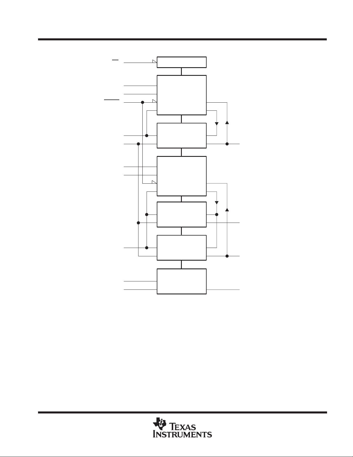
functional block diagram
PD
1PC1
1PC2
DLADJ
SRG1IN
SSR
2,3PC1
2,3PC2
POWER DOWN
PLL1
Phase Control
Phase Control
Delay Adjust
TTL/CCD
S1
SR
PLL2,3
Phase Control
Phase Control
Delay Adjust
TTL/CCD
S2
SR
SRG1OUT
SRG2OUT
SRG2,3IN
TRGIN
TSR
SR
SR
TTL/CCD
S3
SRG3OUT
TTL/CCD
T
TRGOUT
2
POST OFFICE BOX 655303 • DALLAS, TEXAS 75265
TMS3472A
I/O
DESCRIPTION
Phase-adjust control for SRG2OUT, SRG3OUT
Phase-adjust control for SRG1OUT
Positive suppl
oltage
Negative suppl
oltage
SERIAL DRIVER
SOCS025B – FEBRUARY 1991
logic symbol
†
This symbol is in accordance with ANSI/IEEE Std 91-1984.
†
3
PD
SSR
DLADJ
1PC1
1PC2
SRG1IN
2,3PC1
2,3PC2
SRG2,3IN
TRGIN
TSR
9
1
18
19
5
7
8
4
6
11
Pwr Dwn
Ser Slew
Ser Delay Adj
Slew
Phase
Phase
CCD Driver
PLL1
TTL/CCD
[S1]
PLL2,3
TTL/CCD
[S2]
TTL/CCD
[S3]
TTL/CCD
[T]
14
15
16
13
SRG1OUT
SRG2OUT
SRG3OUT
TRGOUT
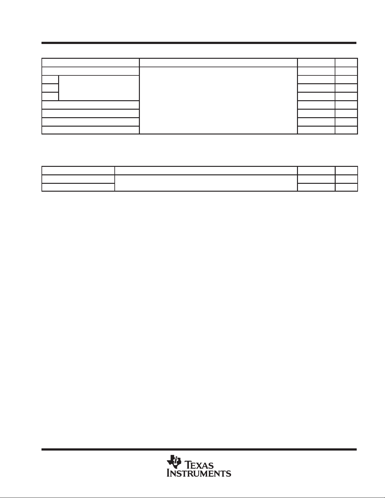
Terminal Functions
TERMINAL
NAME NO.
DLADJ 1 I Delay adjust for all serial-register gates
GND 2 Ground
‡
2,3PC1
‡
2,3PC2
‡
1PC1
‡
1PC2
PD 3 I Power down
SRG1IN 5 I Serial-register gate 2 and 3 in
SRG2,3IN 4 I Serial-register gate 1 in
SRG1OUT 14 O Serial-register gate 1 out
SRG2OUT 15 O Serial-register gate 2 out
SRG3OUT 16 O Serial-register gate 3 out
SSR 9 I Serial-register gate out slew-rate adjust
TRGIN 6 I Transfer gate in
TRGOUT 13 O Transfer gate out
TSR 11 I Transfer gate out slew-rate adjust
§
V
CC
§
V
CC
§
V
SS
§
V
SS
‡
A 270-pF capacitor should be connected between terminals 7 and 8 and between
terminals 18 and 19.
§
All terminals of the same name should be connected together externally.
7 I
8 I
18 I
19 I
12 I
17 I
10 I
20 I
pp
pp
y v
y v
POST OFFICE BOX 655303 • DALLAS, TEXAS 75265
3
TMS3472A
SERIAL DRIVER
SOCS025B – FEBRUARY 1991
absolute maximum ratings over operating free-air temperature range (unless otherwise noted)
Positive supply voltage, V
Negative supply voltage, V
Continuous total power dissipation at (or below), T
Operating free-air temperature range, T
Storage temperature range, T
Lead temperature 1,6 mm (1/16 inch) from case for 10 seconds 260°C. . . . . . . . . . . . . . . . . . . . . . . . . . . . . . .
†
Stresses beyond those listed under “absolute maximum ratings” may cause permanent damage to the device. These are stress ratings only, and
functional operation of the device at these or any other conditions beyond those indicated under “recommended operating conditions” is not
implied. Exposure to absolute-maximum-rated conditions for extended periods may affect device reliability.
NOTES: 1. All voltage values are with respect to GND.
2. The algebraic convention, in which the least positive (most negative) value is designated minimum, is used in this data sheet for
voltage levels only .
(see Note 1) 3 V. . . . . . . . . . . . . . . . . . . . . . . . . . . . . . . . . . . . . . . . . . . . . . . . . . . . . .
CC
(see Note 2) –11.1 V. . . . . . . . . . . . . . . . . . . . . . . . . . . . . . . . . . . . . . . . . . . . . . . . .
SS
≤ 25°C:
A
Unmounted device (see Figure 1) 825 mW. . . . . . . . . . . . . .
Mounted device (see Figure 1) 1150 mW. . . . . . . . . . . . . . . .
–20°C to 45°C. . . . . . . . . . . . . . . . . . . . . . . . . . . . . . . . . . . . . . . . . . .
A
–55°C to 125°C. . . . . . . . . . . . . . . . . . . . . . . . . . . . . . . . . . . . . . . . . . . . . . . . .
STG
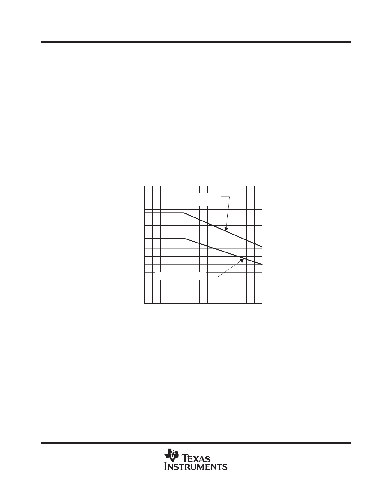
POWER DISSIPATION
vs
1500
1400
1300
1200
1100
1000
900
800
700
600
500
– Power Dissipation – mW
400
D
P
300
200
100
0
0 10203040506070
FREE-AIR TEMPERATURE
Mounted Device
(see Note A)
Unmounted Device
TA – Free-Air Temperature – ° C
†
Figure 1
NOTE A: The mounted-device derating curve of Figure 1 is obtained under the following conditions:
4
The board is 50 mm by 50 mm by 1.6 mm thick.
The board material is glass epoxy.
The copper thickness of all the etch runs is 35 microns.
Etch run dimensions – All 20 etch runs are 0.4 mm by 22 mm.
Each chip is soldered to the board.
An aluminum cooling fin 10 mm by 10 mm by 1 mm thick is coupled to the chip with thermal paste.
POST OFFICE BOX 655303 • DALLAS, TEXAS 75265

TMS3472A
High-level input voltage, V
V
Low-level input voltage, V
V
ISSSupply current
mA
SERIAL DRIVER
SOCS025B – FEBRUARY 1991
recommended operating conditions
MIN NOM MAX UNIT
Positive supply voltage, V
Negative supply voltage, VSS (see Note 2)
p
p
Slope-bias resistance 10 50 kΩ
Operating free-air temperature, T
†
VCC and VSS have 100-mA current limits. Adequate decoupling capacitors are required from these pins to ground.
NOTE 2: The algebraic convention, in which the least positive (most negative) value is designated minimum, is used in this data sheet for voltage
levels only.
CC
IH
IL
†
†
DLADJ, SRG1IN, SRG2,3IN, TRGIN 2 5
PD 2.5 5
DLADJ, SRG1IN, SRG2,3IN, TRGIN 0 0.8
PD 0 0.9
A
0 1 2.2 V
–11.1 –10.4 –9.7 V
–20 45 °C
electrical characteristics over recommended ranges of supply voltage and operating free-air
temperature (unless otherwise noted)
PARAMETER TEST CONDITIONS MIN TYP MAX UNIT
V
High-level output voltage
OH
V
Low-level output voltage
OL
I
High-level input current VIH = 5 V 50 µA
IH
I
Low-level input current VIL = 0 ±10 µA
IL
pp
‡
These parameters are measured with TA = 25°C, VSS = –10.3 V, VCC = 2.1 V, slope-bias resistance on SSR and TSR = 22 kΩ, frequency of
SRG1OUT , SRG2OUT , and SRG3OUT = 4.8 MHz, and frequency of TRGOUT = 2.1 MHz. The load is a TC241 monochrome CCD image sensor .
‡
IOH
IOH
IOL
IOL
No load, PD at 0 V –0.85
Average load –55
= 48 mA (peak),
(serial)
(transfer)
= 48 mA (peak),
(serial)
(transfer)
= 67 mA (peak)
= 32 mA (peak)
VCC–0.5 V
VSS–0.6 V
CCVCC
SSVSS
+0.5 V
+0.8 V
POST OFFICE BOX 655303 • DALLAS, TEXAS 75265
5
TMS3472A
See Note 3
See Note 4
SERIAL DRIVER
SOCS025B – FEBRUARY 1991
switching characteristics for SRG1OUT, SRG2OUT, and SRG3OUT
PARAMETER TEST CONDITIONS MIN MAX UNIT
Jitter 2 ns
t
d1
t
See Figure 2 37 ns
d2
t
d3
t
Pulse duration, high
w(H)
t
Pulse duration, low 65 ns
w(L)
Slew rate 400 V/µs
Noise amplitude 300 mV
NOTE 3: These parameters are measured with TA = 25°C, VSS = –10.3 V , VCC = 2.1 V , slope-bias resistance on SSR = 22 kΩ, and frequency
of SRG1OUT, SRG2OUT, and SRG3OUT = 4.8 MHz. The load is a TC241 monochrome CCD image sensor.
switching characteristics for TRGOUT
PARAMETER TEST CONDITIONS MIN MAX UNIT
t
Rise time
r
t
Fall time
f
NOTE 4: These parameters are measured with TA = 25°C, VSS = –10.3 V , VCC = 2.1 V , slope-bias resistance on TSR = 22 kΩ, and frequency
of TRGOUT = 2.1 MHz. The load is a TC241 monochrome CCD image sensor.
15 30 ns
82 ns
35 ns
135 185 ns
50 100 ns
6
POST OFFICE BOX 655303 • DALLAS, TEXAS 75265

PARAMETER MEASUREMENT INFORMATION
TMS3472A
SERIAL DRIVER
SOCS025B – FEBRUARY 1991
SRG1IN or
SRG2,3IN
SRG1OUT,
SRG2OUT,
or SRG3OUT
50%
VSS + 1.2 V
VSS + 0.8 V
50%
105 ns
t
d1
t
d2
t
d3
VCC – 0.5 V
t
t
w(L)
Noise
300 mV max
w(H)
Figure 2. Serial-Register-Gate Timing Diagram
POST OFFICE BOX 655303 • DALLAS, TEXAS 75265
7

TMS3472A
SERIAL DRIVER
SOCS025B – FEBRUARY 1991
MECHANICAL DATA
DW/R-PDSO-G** PLASTIC WIDE-BODY SMALL-OUTLINE PACKAGE
20 PIN SHOWN
A
20 11
DIM
PINS**
16
20
24
28
0.419 (10,65)
0.400 (10,15)
0.104 (2,65)
0.093 (2,35)
0.012 (0,30)
0.004 (0,10)
0.050 (1,27)
0.299 (7,59)
0.293 (7,45)
A MIN
A MAX
1
0.020 (0,51)
0.014 (0,35)
0.010 (0,25)
10
Seating Plane
0.004 (0,10)
0°–8°
M
0.400
(10,16)
0.410
(10,41)
0.012 (0,30)
0.009 (0,23)
0.500
(12,70)
0.510
(12,95)
0.364 (9,24)
0.338 (8,58)
0.600
(15,24)
0.610
(15,49)
0.700
(17,78)
0.710
(18,03)
0.050 (1,27)
0.016 (0,40)
NOTES: A. All linear dimensions are in inches (millimeters).
8
B. This drawing is subject to change without notice.
C. Body dimensions do not include mold flash or protrusion not to exceed 0.006 (0,15).
POST OFFICE BOX 655303 • DALLAS, TEXAS 75265
4040000/A–10/93

IMPORTANT NOTICE
T exas Instruments and its subsidiaries (TI) reserve the right to make changes to their products or to discontinue
any product or service without notice, and advise customers to obtain the latest version of relevant information
to verify, before placing orders, that information being relied on is current and complete. All products are sold
subject to the terms and conditions of sale supplied at the time of order acknowledgement, including those
pertaining to warranty, patent infringement, and limitation of liability.
TI warrants performance of its semiconductor products to the specifications applicable at the time of sale in
accordance with TI’s standard warranty. Testing and other quality control techniques are utilized to the extent
TI deems necessary to support this warranty . Specific testing of all parameters of each device is not necessarily
performed, except those mandated by government requirements.
CERT AIN APPLICATIONS USING SEMICONDUCTOR PRODUCTS MAY INVOLVE POTENTIAL RISKS OF
DEATH, PERSONAL INJURY, OR SEVERE PROPERTY OR ENVIRONMENTAL DAMAGE (“CRITICAL
APPLICATIONS”). TI SEMICONDUCTOR PRODUCTS ARE NOT DESIGNED, AUTHORIZED, OR
WARRANTED TO BE SUITABLE FOR USE IN LIFE-SUPPORT DEVICES OR SYSTEMS OR OTHER
CRITICAL APPLICA TIONS. INCLUSION OF TI PRODUCTS IN SUCH APPLICATIONS IS UNDERST OOD TO
BE FULLY AT THE CUSTOMER’S RISK.
In order to minimize risks associated with the customer’s applications, adequate design and operating
safeguards must be provided by the customer to minimize inherent or procedural hazards.
TI assumes no liability for applications assistance or customer product design. TI does not warrant or represent
that any license, either express or implied, is granted under any patent right, copyright, mask work right, or other
intellectual property right of TI covering or relating to any combination, machine, or process in which such
semiconductor products or services might be or are used. TI’s publication of information regarding any third
party’s products or services does not constitute TI’s approval, warranty or endorsement thereof.
Copyright 1998, Texas Instruments Incorporated
 Loading...