

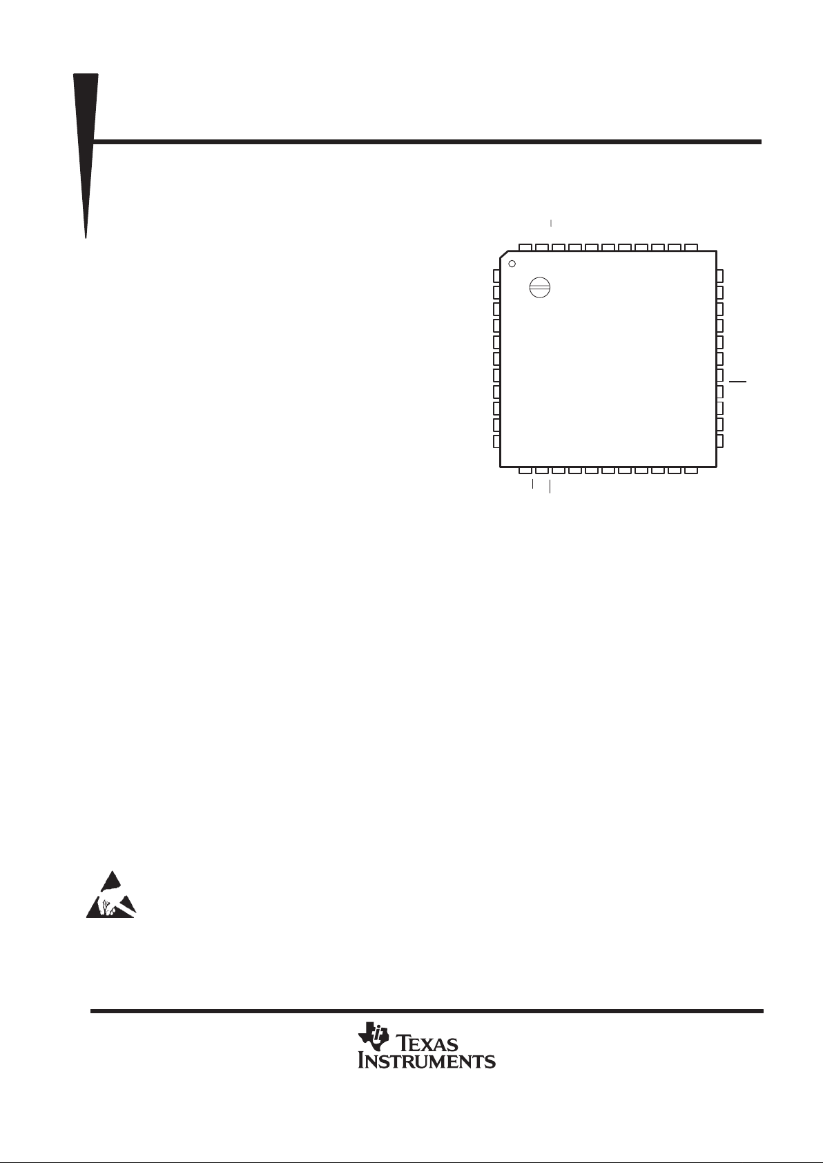
TMS3471C
2/3-INCH NTSC TIMER
SOCS028B – AUGUST 1991
Copyright 1991, Texas Instruments Incorporated
1
POST OFFICE BOX 655303 • DALLAS, TEXAS 75265
• NTSC-Timing Operation
• Solid-State Reliability
• Monochrome Operation
• Eight Selectable-Antiblooming Modes
• Surface-Mount Package
• Clamp-Pulse Select Option
description
The TMS3471C is a monolithic integrated circuit
designed to supply timing signals for the Texas
Instruments (TI) 1 1-mm diagonal TC241 monochrome CCD image sensor. The TMS3471C
supplies both CCD drive signals and NTSC
television synchronization signals at standard
video rates. It requires a single 5-V supply voltage
and a 14.318-MHz crystal-oscillator input. The
TMS3471C provides several options, including
multiple antiblooming modes, clamp-pulse selection, and delayed horizontal transfer.
The TMS3471C is used in conjunction with
level-shifting devices such as the TI TMS3473B
parallel driver and the TI TMS3472A serial driver.
It also supplies sample-and-hold signals for the TI TL1593 three-channel sample-and-hold and multiplex signals
for the TI TL1051 video preprocessor. The TMS3471C NTSC synchronization-signal outputs include composite
sync, composite blank, clamp, subcarrier, subcarrier delayed by 90 degrees, and burst flag.
The TMS3471C is supplied in a 44-pin plastic flat package and is characterized for operation from – 20°C
to 45°C.
This device contains circuits to protect its inputs and outputs against damage due to high static voltages or electrostatic fields. These
circuits have been qualified to protect this device against electrostatic discharges (ESD) of up to 2 kV according to MIL-STD-883C,
Method 3015; however, precautions should be taken to avoid application of any voltage higher than maximum-rated voltages to these
high-impedance circuits. During storage or handling, the device leads should be shorted together or the device should be placed in
conductive foam. In a circuit, unused inputs should always be connected to an appropriate logic voltage level, preferably either VCC or ground.
Specific guidelines for handling devices of this type are contained in the publication
Guidelines for Handling Electrostatic-Discharge-Sensitive
(ESDS) Devices and Assemblies
available from Texas Instruments.
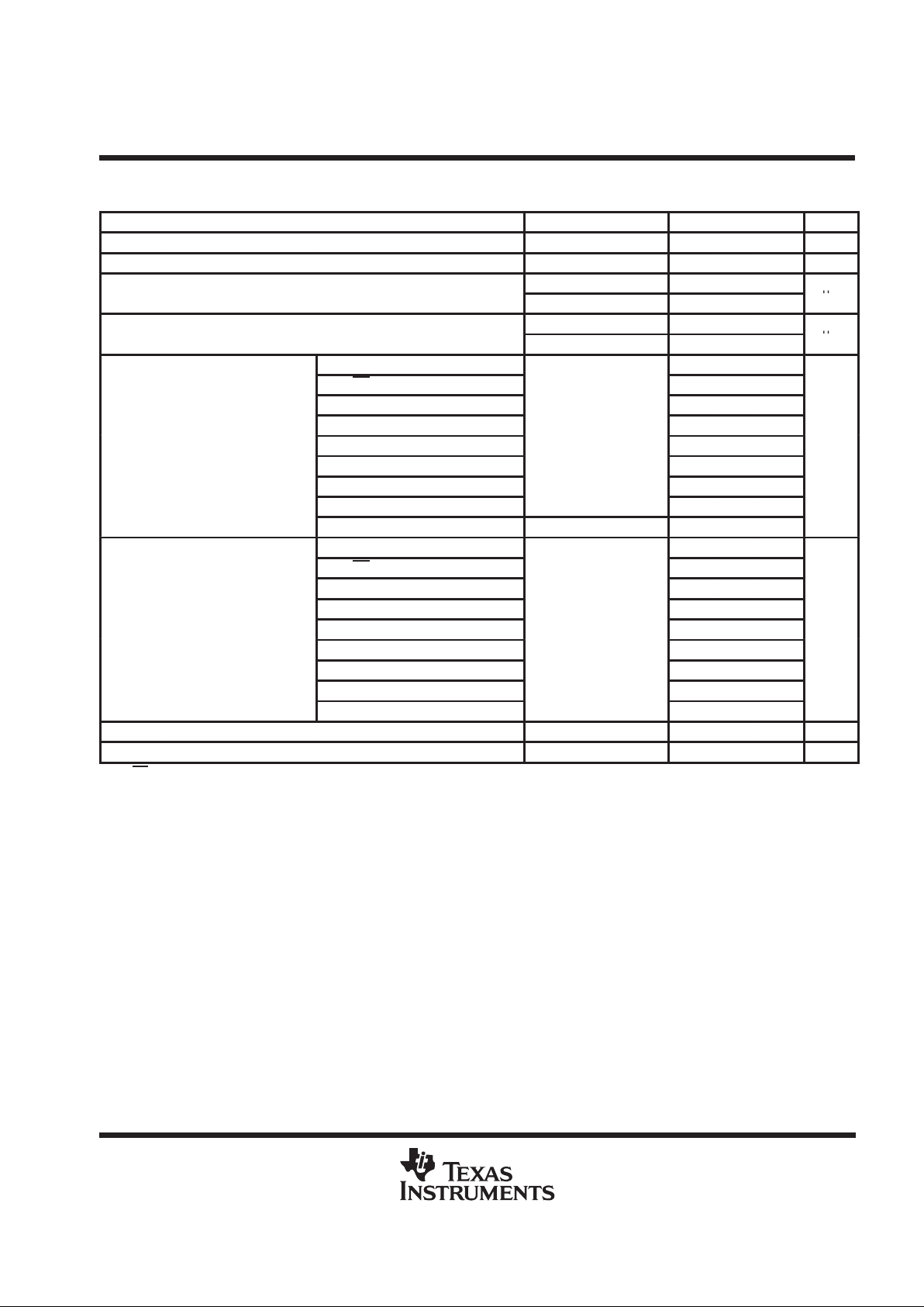
GND
SH1
SH2,3
PI
ABIN
GT
PS
PD
S2,3
S1
T
12 13
1
2
3
4
5
6
7
8
9
10
11
BCP2
CP2
CP1
CSYNC
CBLK
BF
SC
SC(90)
ABS0
ABS1
ABS2
14 15 16 17
FS PACKAGE
(TOP VIEW)
GT2
GT1X2X1
43 42 41 40 3944 38
BCP1FIE/L
VDS
BCPS1
BCPS0
GT3
VGATE
HGATE
CLK2M
V
HIGH
I/N
SB
GP
VD
WHTA
WHTB
36 35 3437
18 19 20 21 22
CC
33
32
31
30
29
28
27
26
25
24
23
PRODUCTION DATA information is current as of publication date.
Products conform to specifications per the terms of Texas Instruments
standard warranty. Production processing does not necessarily include
testing of all parameters.
TI is a trademark of Texas Instruments Incorporated.
TMS3471C
2/3-INCH NTSC TIMER
SOCS028B – AUGUST 1991
2
POST OFFICE BOX 655303 • DALLAS, TEXAS 75265
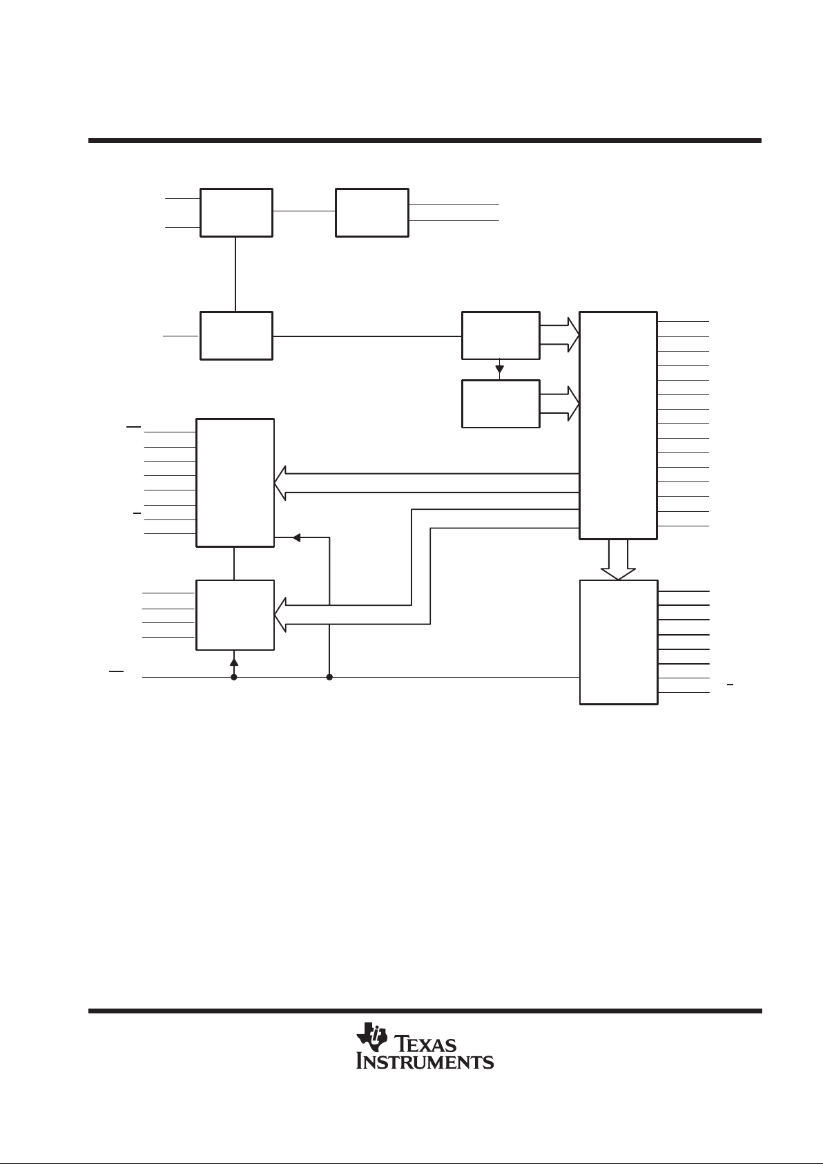
functional block diagram
Oscillator
Divide
by 4
14.318
MHz
3.58 MHz
Horizontal
Counter
Vertical
Counter
Clock
Generator
Antiblooming
Generator
Serial/
Sample-and
-Hold
Generator
Decoder
17
18
16
20
19
5
4
3
2
44
1
6
43
39
40
WHTA
WHTB
VD
HGATE
VGATE
CBLK
CSYNC
CP1
CP2
BCP1
BCP2
BF
FI
BCPS0
BCPS1
S1
S2,3
SH1
SH2,3
GT1
GT2
GT3
E/L
24
25
32
31
36
37
38
42
X1
34
X2
35
8
SC(90)
7
SC
Divide
by 7
2.045 MHz
CLK2M
21
26
28
27
30
23
41
13
15
PD
GT
PS
PI
T
VDS
I/N
GP
29
11
10
9
ABIN
ABS2
ABS1
ABS0
SB
14
The levels on these three terminals determine which of the eight antiblooming modes is selected:
MODE ABS2 ABS1 ABS0 Operation
0LLLNo ABG pulses
1 L L H 250-kHz clocking during flyback only
2 L H L 1-MHz clocking during flyback only
3 L H H 2.2-MHz clocking during flyback only
4 H L L 250-kHz continuous clocking
5 H L H 500-kHz continuous clocking
6 H H L 1-MHz continuous clocking
7 H H H 2.2-MHz continuous clocking
TMS3471C
2/3-INCH NTSC TIMER
SOCS028B – AUGUST 1991
3
POST OFFICE BOX 655303 • DALLAS, TEXAS 75265
Terminal Functions
TERMINAL
NAME NO.
I/O
DESCRIPTION
ABIN 29 O Antiblooming in. ABIN drives the ABG input of the TC240/TC241 CCD image sensors.
ABS0 9 I
ABS1 10 I
ABS2 11 I
BCP1 44 O Optical black clamp pulse 1
BCP2 1 O Optical black clamp pulse 2
BCPS0 39 I
The levels on BCPS0 and BCPS1 determine the placement and duration of the BCP1 and BCP2 pulses
BCPS1 40 I
relative to the horizontal scan timing (see Figure 4 for the truth table for BCPS0 and BCPS1 and for the
corresponding BCP1 and BCP2 pulse placements).
BF 6 O Burst flag
CBLK 5 O Composite blank
CLK2M 21 O 2-MHz clock
CP1 3 O Clamp
CP2 2 O Clamp
CSYNC 4 O Composite sync
E/L 42 I
Delay select for S1 and S2,3. When E/L is high, the two serial-transfer pulses occur early relative to the
sample-and-hold pulses SH1 and SH2,3. When E/L
is low, the two serial-transfer pulses occur late
relative to the sample-and-hold pulses.
FI 43 O Field index
GND 33 Ground
GP 15 I Exposure control: GP gates PS and PI
GT 28 O TMS3473B parallel-driver MIDSEL input switch
GT1 36 O Y gate 1
GT2 37 O Y gate 2
GT3 38 O Y gate 3
HGATE 20 O Decoded H count signal. HGA TE is a test point and is not used in normal operation.
HIGH 12 I Not used (tie high)
I/N 13 I Interlace select. If high, interlace mode is selected; if low, noninterlace mode is selected.
PD 26 O Power down. A low-logic level on PD causes the device to enter a low power-consumption mode.
PI 30 O Parallel-image-area gate clock
PS 27 O Parallel-storage-area gate clock
SB 14 I
Standby-mode select. When SB is high, normal operation is selected; when SB is low, the power-down
mode is selected.
SC 7 O Subcarrier (3.58 MHz)
SC(90) 8 O Subcarrier phase shifted by 90 degrees
SH1 32 O Sample-and-hold pulse 1
SH2,3 31 O Sample-and-hold pulse 2, 3
TMS3471C
2/3-INCH NTSC TIMER
SOCS028B – AUGUST 1991
4
POST OFFICE BOX 655303 • DALLAS, TEXAS 75265
Terminal Functions (Continued)
TERMINAL
NAME NO.
I/O
DESCRIPTION
S1 24 O Serial clock 1
S2,3 25 O Serial clock 2, 3
T 23 O Transfer-gate clock
V
CC
22 DC power
VD 16 O Vertical drive
VDS 41 I
Vertical-dump speed. When VDS is high, the vertical-dump frequency is 2MHz; when VDS is low, the
vertical-dump frequency is 1 MHz. VDS can also function as a timer reset by dropping the voltage on
VDS from VCC to VCC/2 and then raising it back to VCC.
VGATE 19 O Decoded V count signal. VGATE is a test point and is not used in normal operation.
WHTA 17 O WHTA is a test point and is not used in normal operation.
WHTB 18 O WHTB is a test point and is not used in normal operation.
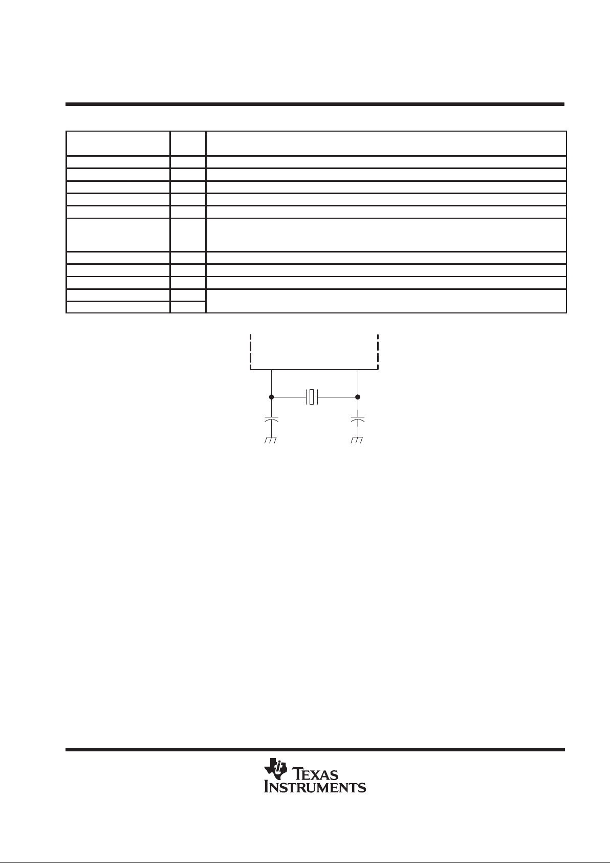
X1 34
X2 35
Crystal oscillator (see Figure 1)
X1 X2
34 35
C1 ≈ 40 pF C2 ≈ 40 pF
TMS3471C
NOTE: The TMS3471C is designed for use with
a crystal oscillator. The X1 and X2
terminals should not connect directly to
external driver outputs.
Figure 1. Connection of an External Crystal Oscillator to the TMS3471C
TMS3471C
2/3-INCH NTSC TIMER
SOCS028B – AUGUST 1991
5
POST OFFICE BOX 655303 • DALLAS, TEXAS 75265
absolute maximum ratings over operating free-air temperature range (unless otherwise noted)
†
Supply voltage, V
CC
(see Note 1) 7 V. . . . . . . . . . . . . . . . . . . . . . . . . . . . . . . . . . . . . . . . . . . . . . . . . . . . . . . . . . . . .
Input voltage range, V
I
–0.3 V to VCC + 0.3 V. . . . . . . . . . . . . . . . . . . . . . . . . . . . . . . . . . . . . . . . . . . . . . . . . . . . . .
Output voltage range, V
O
–0.3 V to VCC + 0.3 V. . . . . . . . . . . . . . . . . . . . . . . . . . . . . . . . . . . . . . . . . . . . . . . . . . .
Continuous total power dissipation: T
A
= 25°C 550 mW. . . . . . . . . . . . . . . . . . . . . . . . . . . . . . . . . . . . . . . . . . .
T
A
= 45°C 440 mW. . . . . . . . . . . . . . . . . . . . . . . . . . . . . . . . . . . . . . . . . . .
T
A
= 75°C 275 mW. . . . . . . . . . . . . . . . . . . . . . . . . . . . . . . . . . . . . . . . . . .
Operating free-air temperature range, T
A
–20°C to 45°C. . . . . . . . . . . . . . . . . . . . . . . . . . . . . . . . . . . . . . . . . . . .
Storage temperature range –55°C to 125° C. . . . . . . . . . . . . . . . . . . . . . . . . . . . . . . . . . . . . . . . . . . . . . . . . . . . . . .
Lead temperature 1,6 mm (1/16 inch) from case for 10 seconds 260°C. . . . . . . . . . . . . . . . . . . . . . . . . . . . . . .
Lead temperature 1,6 mm (1/16 inch) from case for 3 seconds 350°C. . . . . . . . . . . . . . . . . . . . . . . . . . . . . . . . .
†
Stresses beyond those listed under “absolute maximum ratings” may cause permanent damage to the device. These are stress ratings only, and
functional operation of the device at these or any other conditions beyond those indicated under “recommended operating conditions” is not
implied. Exposure to absolute-maximum-rated conditions for extended periods may affect device reliability.
NOTE 1: All voltage values are with respect to GND.
recommended operating conditions
MIN NOM MAX UNIT
Supply voltage, V
CC
4.5 5 5.5 V
High-level input voltage, V
IH
V
Low-level input voltage, V
IL
0.8 V
Operating frequency 14.31818 MHz
Power-up time 300 µs
Operating free-air temperature, T
A
–20 45 °C
TMS3471C
2/3-INCH NTSC TIMER
SOCS028B – AUGUST 1991
6
POST OFFICE BOX 655303 • DALLAS, TEXAS 75265
electrical characteristics over recommended ranges of supply voltage and operating free-air
temperature, V
CC
= 5 V (unless otherwise noted)
†
PARAMETER TEST CONDITIONS MIN TYP MAX UNIT
V
OH
High-level output voltage IOH <1 µA 4.95 V
V
OL
Low-level output voltage IOL <1 µA 0.05 V
p
VCC = 5 V 75
I
IH
‡
High-level input current
VCC = 4.5 V 65
µ
A
p
VCC = 5.5 V 225
IILLow-level input current
VCC = 5 V 200
µ
A
S1, T, ABIN, PS, PI, GT –0.1
S2,3, PD –0.2
SH1, GT1, GT2, GT3 –2.5
SH2,3
–5
I
OH
High-level output current BCP1, BCP2
V
OH
= 3.5
V
–1 mA
SC, SC(90) –3
CP2 –0.6
CLK2M –0.3
All other outputs VOH= 4.6 V –0.5
S1, T, ABIN, PS, PI, GT 0.1
S2,3, PD 0.2
SH1, GT1, GT2, GT3 2.5
SH2,3 5
I
OL
Low-level output current BCP1, BCP2 VOL= 0.4 V 1 mA
SC, SC(90) 0.3
CP2 0.6
CLK2M 0.3
All other outputs 0.5
I
CC(AV)
Average supply current 40 mA
I
CC(S)
Standby supply current 15 mA
†
The SB input is a Schmitt-trigger input with 0.5-V to 1-V hysteresis.
‡
All inputs have pullup-current sources.

TMS3471C
2/3-INCH NTSC TIMER
SOCS028B – AUGUST 1991
7
POST OFFICE BOX 655303 • DALLAS, TEXAS 75265
switching characteristics over recommended operating free-air temperature range, VCC = 5 V
PARAMETER TEST CONDITIONS MIN TYP MAX UNIT
S1 CL= 20 pF 10
S2,3 CL= 40 pF 10
ABIN, GT, PD, PI, PS, T
p
30
GT1, GT2, GT3, SH1
C
L
= 20
pF
10
t
r
Rise time SH2,3 CL= 40 pF 10 ns
BCP1, BCP2 CL= 50 pF 100
SC, SC(90) CL= 15 pF 30
CLK2M
p
50
All other outputs
C
L
= 50
pF
200
S1 CL= 20 pF 8
S2,3 CL= 40 pF 8
ABIN, GT, PD, PI, PS, T
p
30
GT1, GT2, GT3, SH1
C
L
= 20
pF
8
t
f
Fall time SH2,3 CL= 40 pF 8 ns
BCP1, BCP2 CL= 50 pF 100
SC, SC(90) CL= 15 pF 30
CLK2M
p
50
All other outputs
C
L
= 50
pF
100
S1 rising edge to S2,3 rising edge ±5
S1 falling edge to SH1 falling edge –3 –8 –13
S1 rising edge to GT1 falling edge –3 –8 –13
SH2,3 rising edge to GT1 rising edge ±5
t
sk(o)
Skew time
S2,3 falling edge to SH2,3 falling edge –3 –8 –13
ns
S2,3 falling edge to GT2 rising edge –3 –8 –13
SH2,3 falling edge to GT2 rising edge ±5
SH2,3 rising edge to GT3 falling edge ±5
tw–tc/2
Pulse duration compared to
pulse duration at 50% duty
cycle
†
S1 or S2, 3 ±5 ns
†
The S1 and S2,3 outputs ideally exhibit a 50% duty cycle. This parameter indicates how much the duty cycle may shift while a constant cycle
time is maintained. For example, for a 210-ns cycle time, t
w(H)
= 110 ns and t
w(L)
= 100 ns are possible.

TMS3471C
2/3-INCH NTSC TIMER
SOCS028B – AUGUST 1991
8
POST OFFICE BOX 655303 • DALLAS, TEXAS 75265
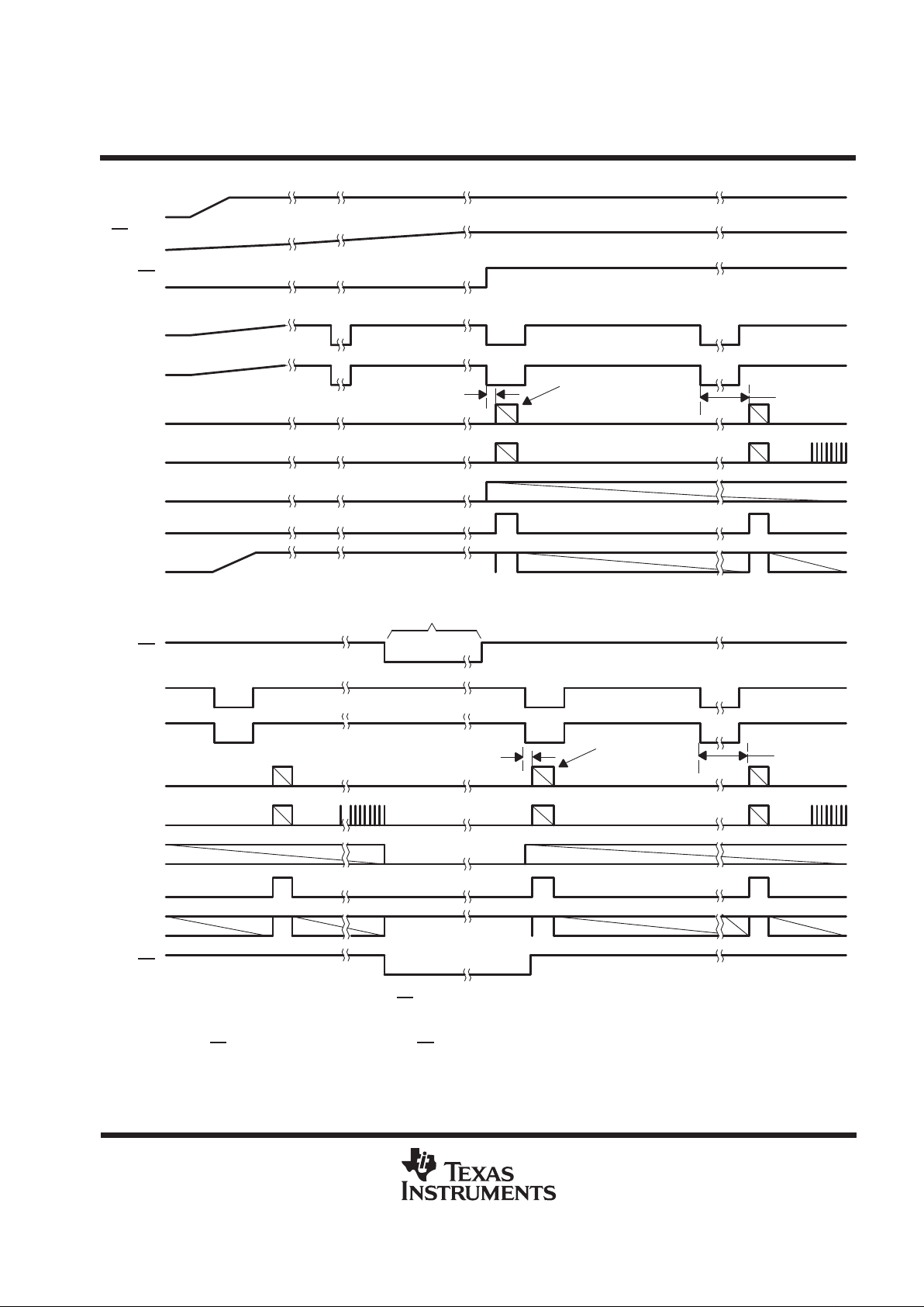
PARAMETER MEASUREMENT INFORMATION
1 Line = 63.55 µs
(525)
PS,T
ABIN
GT
PI
SH2,3
GT3
S1
SC,SC(90)
BCP2
BCP1
BF
CBLK
CSYNC
CP2
CP1
FI
VD
523
521
279262
524
9
0
0
Continuous
VS 3H
EQ 3H
EQ 3H
VS 3H
EQ 3H
20
0
272
9
524
Even Field
Odd Field, 262.5 H
0
268.5
262.5
60
288
280275270265
302520151050
17
S2,3
0
GT2
9
0
GT1
9
0
SH1
6H 6H
20H
10H
20H
10H
244 Pulses
‡
244 Pulses
‡
244
Pulses
‡
244
Pulses
‡
Vertical
Scale
†
10H10H
4.77273 MHz
260256
EQ 3H
262
†
525 intervals equal 33.3 ms equals 1 TV frame
‡
The frequency of these pulses is either 2.04545 MHz or 1.02273 MHz and is determined by the logic level on the VDS input.
Figure 2. Vertical Timing

TMS3471C
2/3-INCH NTSC TIMER
SOCS028B – AUGUST 1991
9
POST OFFICE BOX 655303 • DALLAS, TEXAS 75265
T
PS
HGATE
BCP2
BCP1
BF
CBLK
CP2
CP1
Horizontal
Scale
†
(130)
20
14
22
0
133
20.50
133
70656056302520151050125
120
95
3 5 7 9 111
13
CSYNC
PI
1/2 Active
1/2 Active
Dummy
6 X 3
Dark
8 X 3 –1
Active
252 X 3 –2 = 754
S1
S2, 3
SH1
SH2, 3
GT1
GT2
GT3
OUT1
OUT2
OUT3
75
Output From
CCD Image
Sensor
†
130 intervals equal 63.55 µs equals one horizontal-scan line
Figure 3. Horizontal Timing

TMS3471C
2/3-INCH NTSC TIMER
SOCS028B – AUGUST 1991
10
POST OFFICE BOX 655303 • DALLAS, TEXAS 75265
0
0
2 4 6 8 10 12 14 16 18 20 22 24 26 28 30122 124 126 128
20 40 60 80 100 120 140 160 180850 870 890 200 220
126 133
119 140
122.5 136.5
129.5
143.5
MODE 0
MODE 1
MODE 2
MODE 3
CBLK
MODE 0
MODE 1
MODE 2
MODE 3
MODE 0
MODE 1
MODE 2
MODE 3
MODE 5
MODE 4
MODE 6
MODE 7
ABIN BCP1BCP2
(910)
(130)
†
‡
†
910 intervals equal 63.55 µs equals one horizontal-scan line
‡
130 intervals equal 63.55 µs equals one horizontal-scan line
MODE
0 1 2 3 MODE 0 1 2 3 4 5 6 7
BCPS1 L L H H ABS2 L L L L H H H H
BCPS0 L H L H ABS1 L L H H L L H H
ABS0 L H L H L H L H
Figure 4. ABIN, BCP1, BCP2 Timing at the Start of H

TMS3471C
2/3-INCH NTSC TIMER
SOCS028B – AUGUST 1991
11
POST OFFICE BOX 655303 • DALLAS, TEXAS 75265
24424312
24424321
DPI
ABIN
GT
PI
PS
T
Vertical-Dump
Frequency
(2.04545 MHz
or 1.02273 MHz)
(see Note A)
Odd Field
(see Note B)
Even Field
GP
DAB
tr ≤ 2H
NOTES: A. When the vertical-dump frequency is 1.02273 MHz, PI, PS, and T have a 50% duty cycle.
B. If I/N
is low, the DPI waveform is always as shown for the odd-field case.
Figure 5. PI, PS, T, and ABIN Timing

TMS3471C
2/3-INCH NTSC TIMER
SOCS028B – AUGUST 1991
12
POST OFFICE BOX 655303 • DALLAS, TEXAS 75265
20
130 178 192 195 260125 128 262
8
VS
EQ
CBLK
BCP1
CP1
BCP2
0 5 10 1583 96 100 125
(130)
25 52 55 60 65 65
123
313
3
13
22
0
2014
20.5
0
CSYNC
BF
CP2
2017
20.517.5
SH1,
SH2,3
PS
1311
11
97531
0
S1, S2,3
0 14
HGATE
397
20.5
100
WHTA
20.5
20.5
83
WHTB
175
262.5
258.5
WHTA
WHTB
VD
VGATE
Vertical
Scale
‡
PI
T
Horizontal
Scale
†
†
130 intervals equal 63.55 µs equals one horizontal-scan line
‡
525 intervals equal 33.33 ms equals one TV frame
Figure 6. H Timing and WHTA, WHTB (V,H) Timing
TMS3471C
2/3-INCH NTSC TIMER
SOCS028B – AUGUST 1991
13
POST OFFICE BOX 655303 • DALLAS, TEXAS 75265
Refresh Pulses
PD
ABIN
GT
S1, S2,3
PS, T
244 Pulses
(see Note C)
PI
SB
See Note D
Standby Operation
ABIN
GT
S1, S2,3
PS, T
244 Pulses256 Pulses
PI
PD
SB (see
Note A)
Power
Power-Up Operation
VD (see
Note B)
VD (see
Note B)
GP
Refresh Pulses
(see Note C)
GP
244
256
0.5 H
6.5 H
256 Pulses
256
0.5 H
244
NOTES: A. A 0.1-µF capacitor is connected between SB and GND.
B. The VD output is fed back to GP.
C. The 256 CCD refresh pulses are generated on PI, PS, and T even if VD is not fed back to GP.
D. When SB
is low, PI, PS, T, S1, S2,3, GT, and PD are all low and ABIN is high.
Figure 7. Power-Up and Standby Timing

TMS3471C
2/3-INCH NTSC TIMER
SOCS028B – AUGUST 1991
14
POST OFFICE BOX 655303 • DALLAS, TEXAS 75265
20
VDS
VD
SB
0 5 10 15 25
PI
ABIN
0.5 H
PS
256 Pulses
GT
PD
1 field
V
CC
1/2 V
CC
GND
S1, S2,3
When VD is High
20
VDS
VD
0 5 10 15 25
PI
ABIN
0.5 H
PS
244 Pulses
GT
PD
6H
V
CC
1/2 V
CC
GND
S1, S2,3
30 35
When VD is Low
Figure 8. Timing for VDS in the Reset Mode

TMS3471C
2/3-INCH NTSC TIMER
SOCS028B – AUGUST 1991
15
POST OFFICE BOX 655303 • DALLAS, TEXAS 75265
GP
PI
GT
PS, T
256 Pulses
(see Note B)
6.5H
VD
ABIN
0.5H
BCP1,
BCP2
244 Pulses
(see Note A)
Normal Operation Clear Operation
(operation
mode)
NOTES: A. When VD is low and GP goes low, 244 pulses are generated on PI, PS, and T.
B. If VD is high and not fed back to GP, then pulsing GP results in 256 pulses being generated on PI, PS, and T. This can be useful
in clearing the imager. An external logic circuit is used to pulse GP.
Figure 9. GP Timing for Normal and Clear Modes

TMS3471C
2/3-INCH NTSC TIMER
SOCS028B – AUGUST 1991
16
POST OFFICE BOX 655303 • DALLAS, TEXAS 75265
20
0111520
25
22
V
CC
0 5 10 15 27026025
4
262 265 275 280 285
V
SS
V
mid
DPI
(interlace)
V
CC
V
SS
DPI
(noninterlace)
V
CC
V
SS
DPS
V
CC
V
SS
DS1, 2, 3
V
ABG+
V
ABG–
AB
mid
DAB
V
ABG–
DAB (mode 0)
V
ABG+
V
ABG–
DAB (mode 4–
mode 7)
V
ABG+
V
ABG–
DAB (mode 1–
mode 3)
‡
Horizontal
Scale
Vertical
Scale
†
†
525 intervals equal 33.33 ms equals one TV frame
‡
130 intervals equal 63.55 µs equals one horizontal-scan line
Figure 10. DPI, DPS, DS, and DAB Drive Timing

TMS3471C
2/3-INCH NTSC TIMER
SOCS028B – AUGUST 1991
17
POST OFFICE BOX 655303 • DALLAS, TEXAS 75265
110105100
SH1
S1
± 5 ns
S2,3
S1
S2,3
SH2,3
GT1
GT2
GT3
± 5 ns
± 5 ns
± 5 ns
Acceptable
8 ± 5 ns
8 ± 5 ns
8 ± 5 ns
8 ± 5 ns
E/L
: H
E/L: L
†
†
Each interval equals one master clock interval equals 69.84 ns.
Figure 11. S1, S2,3, SH1, SH2,3, and GTn Waveforms

TMS3471C
2/3-INCH NTSC TIMER
SOCS028B – AUGUST 1991
18
POST OFFICE BOX 655303 • DALLAS, TEXAS 75265
MECHANICAL DATA
FS/S-PQFP-G44 PLASTIC QUAD FLATPACK
4040160/A–10/93
1,50
1,10
18,20
17,40
33 23
34
44
111
22
12
2,30 MAX
0,10
0,20
1,00 TYP
SQ
14,20 MAX SQ
2,20 MAX
0,55 MAX
0°–10°
Seating Plane
0,10 MIN
0,10
NOTES: A. All linear dimensions are in millimeters.
B. This drawing is subject to change without notice.

IMPORTANT NOTICE
T exas Instruments and its subsidiaries (TI) reserve the right to make changes to their products or to discontinue
any product or service without notice, and advise customers to obtain the latest version of relevant information
to verify, before placing orders, that information being relied on is current and complete. All products are sold
subject to the terms and conditions of sale supplied at the time of order acknowledgement, including those
pertaining to warranty, patent infringement, and limitation of liability.
TI warrants performance of its semiconductor products to the specifications applicable at the time of sale in
accordance with TI’s standard warranty. Testing and other quality control techniques are utilized to the extent
TI deems necessary to support this warranty. Specific testing of all parameters of each device is not necessarily
performed, except those mandated by government requirements.
CERT AIN APPLICATIONS USING SEMICONDUCTOR PRODUCTS MAY INVOLVE POTENTIAL RISKS OF
DEATH, PERSONAL INJURY, OR SEVERE PROPERTY OR ENVIRONMENTAL DAMAGE (“CRITICAL
APPLICATIONS”). TI SEMICONDUCTOR PRODUCTS ARE NOT DESIGNED, AUTHORIZED, OR
WARRANTED TO BE SUITABLE FOR USE IN LIFE-SUPPORT DEVICES OR SYSTEMS OR OTHER
CRITICAL APPLICATIONS. INCLUSION OF TI PRODUCTS IN SUCH APPLICA TIONS IS UNDERST OOD TO
BE FULLY AT THE CUSTOMER’S RISK.
In order to minimize risks associated with the customer’s applications, adequate design and operating
safeguards must be provided by the customer to minimize inherent or procedural hazards.
TI assumes no liability for applications assistance or customer product design. TI does not warrant or represent
that any license, either express or implied, is granted under any patent right, copyright, mask work right, or other
intellectual property right of TI covering or relating to any combination, machine, or process in which such
semiconductor products or services might be or are used. TI’s publication of information regarding any third
party’s products or services does not constitute TI’s approval, warranty or endorsement thereof.
Copyright 1998, Texas Instruments Incorporated
 Loading...