

Page 1

TMS3320C5515 DSP System
User's Guide
Literature Number: SPRUFX5A
October 2010–Revised November 2010
Page 2

2
SPRUFX5A–October 2010–Revised November 2010
Submit Documentation Feedback
Copyright © 2010, Texas Instruments Incorporated
Page 3

Contents
Preface ....................................................................................................................................... 9
1 System Control ................................................................................................................. 13
1.1 Introduction ................................................................................................................. 13
1.1.1 Block Diagram .................................................................................................... 13
1.1.2 CPU Core .......................................................................................................... 14
1.1.3 FFT Hardware Accelerator ...................................................................................... 14
1.1.4 Power Management .............................................................................................. 15
1.1.5 Peripherals ........................................................................................................ 15
1.2 System Memory ........................................................................................................... 16
1.2.1 Program/Data Memory Map ..................................................................................... 16
1.2.2 I/O Memory Map .................................................................................................. 20
1.3 Device Clocking ............................................................................................................ 20
1.3.1 Overview ........................................................................................................... 20
1.3.2 Clock Domains .................................................................................................... 23
1.4 System Clock Generator ................................................................................................. 23
1.4.1 Overview ........................................................................................................... 23
1.4.2 Functional Description ........................................................................................... 24
1.4.3 Configuration ...................................................................................................... 26
1.4.4 Clock Generator Registers ...................................................................................... 29
1.5 Power Management ....................................................................................................... 33
1.5.1 Overview ........................................................................................................... 33
1.5.2 Power Domains ................................................................................................... 33
1.5.3 Clock Management ............................................................................................... 34
1.5.4 Static Power Management ...................................................................................... 46
1.5.5 Power Configurations ............................................................................................ 50
1.6 Interrupts .................................................................................................................... 53
1.6.1 IFR and IER Registers ........................................................................................... 54
1.6.2 Interrupt Timing ................................................................................................... 55
1.6.3 Timer Interrupt Aggregation Flag Register (TIAFR) [1C14h] ............................................... 56
1.6.4 GPIO Interrupt Enable and Aggregation Flag Registers .................................................... 56
1.6.5 DMA Interrupt Enable and Aggregation Flag Registers ..................................................... 56
1.7 System Configuration and Control ...................................................................................... 57
1.7.1 Overview ........................................................................................................... 57
1.7.2 Device Identification .............................................................................................. 57
1.7.3 Device Configuration ............................................................................................. 61
1.7.4 DMA Controller Configuration ................................................................................... 70
1.7.5 Peripheral Reset .................................................................................................. 73
1.7.6 EMIF and USB Byte Access .................................................................................... 75
1.7.7 EMIF Clock Divider Register (ECDR) [1C26h] ............................................................... 77
SPRUFX5A–October 2010–Revised November 2010 Contents
Submit Documentation Feedback
Copyright © 2010, Texas Instruments Incorporated
3
Page 4

www.ti.com
List of Figures
1-1. Functional Block Diagram ................................................................................................ 13
1-2. DSP Memory Map ........................................................................................................ 17
1-3. DSP Clocking Diagram .................................................................................................. 22
1-4. Clock Generator ........................................................................................................... 24
1-5. CLKOUT Control Source Select Register (CCSSR) [1C24h]........................................................ 25
1-6. Clock Generator Control Register 1 (CGCR1) [1C20h] .............................................................. 30
1-7. Clock Generator Control Register 2 (CGCR2) [1C21h] .............................................................. 30
1-8. Clock Generator Control Register 3 (CGCR3) [1C22h] .............................................................. 31
1-9. Clock Generator Control Register 4 (CGCR4) [1C23h] .............................................................. 31
1-10. Clock Configuration Register 1 (CCR1) [1C1Eh]...................................................................... 32
1-11. Clock Configuration Register 2 (CCR2) [1C1Fh]...................................................................... 32
1-12. Idle Configuration Register (ICR) [0001h].............................................................................. 36
1-13. Idle Status Register (ISTR) [0002h]..................................................................................... 37
1-14. Peripheral Clock Gating Configuration Register 1 (PCGCR1) [1C02h] ............................................ 39
1-15. Peripheral Clock Gating Configuration Register 2 (PCGCR2) [1C03h] ............................................ 41
1-16. Peripheral Clock Stop Request/Acknowledge Register (CLKSTOP) [1C3Ah] .................................... 42
1-17. USB System Control Register (USBSCR) [1C32h] ................................................................... 44
1-18. RTC Power Management Register (RTCPMGT) [1930h]............................................................ 46
1-19. RTC Interrupt Flag Register (RTCINTFL) [1920h] .................................................................... 47
1-20. RAM Sleep Mode Control Register1 [0x1C28] ........................................................................ 48
1-21. RAM Sleep Mode Control Register2 [0x1C2A]........................................................................ 49
1-22. RAM Sleep Mode Control Register3 [0x1C2B]........................................................................ 49
1-23. RAM Sleep Mode Control Register4 [0x1C2C]........................................................................ 49
1-24. RAM Sleep Mode Control Register5 [0x1C2D]........................................................................ 49
1-25. IFR0 and IER0 Bit Locations............................................................................................. 54
1-26. IFR1 and IER1 Bit Locations............................................................................................. 55
1-27. Die ID Register 0 (DIEIDR0) [1C40h]................................................................................... 58
1-28. Die ID Register 1 (DIEIDR1) [1C41h]................................................................................... 58
1-29. Die ID Register 2 (DIEIDR2) [1C42h]................................................................................... 58
1-30. Die ID Register 3 (DIEIDR3[15:0]) [1C43h] ............................................................................ 59
1-31. Die ID Register 4 (DIEIDR4) [1C44h]................................................................................... 59
1-32. Die ID Register 5 (DIEIDR5) [1C45h]................................................................................... 59
1-33. Die ID Register 6 (DIEIDR6) [1C46h]................................................................................... 60
1-34. Die ID Register 7 (DIEIDR7) [1C47h]................................................................................... 60
1-35. External Bus Selection Register (EBSR) [1C00h]..................................................................... 61
1-36. RTC Power Management Register (RTCPMGT) [1930h]............................................................ 63
1-37. LDO Control Register (LDOCNTL) [7004h] ............................................................................ 65
1-38. Output Slew Rate Control Register (OSRCR) [1C16h]............................................................... 66
1-39. Pull-Down Inhibit Register 1 (PDINHIBR1) [1C17h] .................................................................. 67
1-40. Pull-Down Inhibit Register 2 (PDINHIBR2) [1C18h] .................................................................. 68
1-41. Pull-Down Inhibit Register 3 (PDINHIBR3) [1C19h] .................................................................. 69
1-42. DMA Interrupt Flag Register (DMAIFR) [1C30h] ...................................................................... 72
1-43. DMA Interrupt Enable Register (DMAIER) [1C31h]................................................................... 72
1-44. DMAn Channel Event Source Register 1 (DMAnCESR1) [1C1Ah, 1C1Ch, 1C36h, and 1C38h] .............. 73
1-45. DMAn Channel Event Source Register 2 (DMAnCESR2) [1C1Bh, 1C1Dh, 1C37h, and 1C39h] .............. 73
1-46. Peripheral Software Reset Counter Register (PSRCR) [1C04h].................................................... 74
1-47. Peripheral Reset Control Register (PRCR) [1C05h].................................................................. 74
4
List of Figures SPRUFX5A–October 2010–Revised November 2010
Copyright © 2010, Texas Instruments Incorporated
Submit Documentation Feedback
Page 5

www.ti.com
1-48. EMIF System Control Register (ESCR) [1C33h] ...................................................................... 76
1-49. EMIF Clock Divider Register (ECDR) [1C26h] ........................................................................ 77
SPRUFX5A–October 2010–Revised November 2010 List of Figures
Submit Documentation Feedback
Copyright © 2010, Texas Instruments Incorporated
5
Page 6

www.ti.com
List of Tables
1-1. ............................................................................................................................... 14
1-2. DARAM Blocks ............................................................................................................ 17
1-3. SARAM Blocks............................................................................................................. 18
1-4. SAROM Blocks ............................................................................................................ 19
1-5. PLL Output Frequency Configuration................................................................................... 24
1-6. CLKOUT Control Source Select Register (CCSSR) Field Descriptions............................................ 25
1-7. Clock Generator Control Register Bits Used In BYPASS MODE................................................... 27
1-8. Output Frequency in Bypass Mode ..................................................................................... 27
1-9. Clock Generator Control Register Bits Used In PLL Mode .......................................................... 27
1-10. PLL Clock Frequency Ranges........................................................................................... 28
1-11. Examples of Selecting a PLL MODE Frequency, When CLK_SEL=L ............................................. 29
1-12. Clock Generator Registers ............................................................................................... 29
1-13. Clock Generator Control Register 1 (CGCR1) Field Descriptions .................................................. 30
1-14. Clock Generator Control Register 2 (CGCR2) Field Descriptions .................................................. 30
1-15. Clock Generator Control Register 3 (CGCR3) Field Descriptions .................................................. 31
1-16. Clock Generator Control Register 4 (CGCR4) Field Descriptions .................................................. 31
1-17. Clock Configuration Register 1 (CCR1) Field Descriptions.......................................................... 32
1-18. Clock Configuration Register 2 (CCR2) Field Descriptions.......................................................... 32
1-19. Power Management Features ........................................................................................... 33
1-20. DSP Power Domains...................................................................................................... 34
1-21. Idle Configuration Register (ICR) Field Descriptions ................................................................. 36
1-22. Idle Status Register (ISTR) Field Descriptions ........................................................................ 37
1-23. CPU Clock Domain Idle Requirements................................................................................. 37
1-24. Peripheral Clock Gating Configuration Register 1 (PCGCR1) Field Descriptions ................................ 39
1-25. Peripheral Clock Gating Configuration Register 2 (PCGCR2) Field Descriptions ................................ 41
1-26. Peripheral Clock Stop Request/Acknowledge Register (CLKSTOP) Field Descriptions......................... 42
1-27. USB System Control Register (USBSCR) Field Descriptions ....................................................... 44
1-28. RTC Power Management Register (RTCPMGT) Field Descriptions ............................................... 46
1-29. RTC Interrupt Flag Register (RTCINTFL) Field Descriptions........................................................ 47
1-30. On-Chip Memory Standby Modes....................................................................................... 48
1-31. Power Configurations ..................................................................................................... 50
1-32. Interrupt Table ............................................................................................................. 53
1-33. IFR0 and IER0 Bit Descriptions ......................................................................................... 54
1-34. IFR1 and IER1 Bit Descriptions ......................................................................................... 55
1-35. Die ID Registers ........................................................................................................... 57
1-36. Die ID Register 0 (DIEIDR0) Field Descriptions....................................................................... 58
1-37. Die ID Register 1 (DIEIDR1) Field Descriptions....................................................................... 58
1-38. Die ID Register 2 (DIEIDR2) Field Descriptions....................................................................... 58
1-39. Die ID Register 3 (DIEIDR3[15:0]) Field Descriptions................................................................ 59
1-40. Die ID Register 4 (DIEIDR4) Field Descriptions....................................................................... 59
1-41. Die ID Register 5 (DIEIDR5) Field Descriptions....................................................................... 59
1-42. Die ID Register 6 (DIEIDR6) Field Descriptions....................................................................... 60
1-43. Die ID Register 7 (DIEIDR7) Field Descriptions....................................................................... 60
1-44. EBSR Register Bit Descriptions Field Descriptions................................................................... 62
1-45. RTCPMGT Register Bit Descriptions Field Descriptions............................................................. 64
1-46. LDOCNTL Register Bit Descriptions Field Descriptions.............................................................. 65
1-47. LDO Controls Matrix ...................................................................................................... 65
6
List of Tables SPRUFX5A–October 2010–Revised November 2010
Copyright © 2010, Texas Instruments Incorporated
Submit Documentation Feedback
Page 7

www.ti.com
1-48. Output Slew Rate Control Register (OSRCR) Field Descriptions................................................... 66
1-49. Pull-Down Inhibit Register 1 (PDINHIBR1) Field Descriptions ...................................................... 67
1-50. Pull-Down Inhibit Register 2 (PDINHIBR2) Field Descriptions ...................................................... 68
1-51. Pull-Down Inhibit Register 3 (PDINHIBR3) Field Descriptions ...................................................... 69
1-52. Channel Synchronization Events for DMA Controllers ............................................................... 71
1-53. System Registers Related to the DMA Controllers ................................................................... 71
1-54. DMA Interrupt Flag Register (DMAIFR) Field Descriptions.......................................................... 72
1-55. DMA Interrupt Enable Register (DMAIER) Field Descriptions....................................................... 72
1-56. DMAn Channel Event Source Register 1 (DMAnCESR1) Field Descriptions ..................................... 73
1-57. DMAn Channel Event Source Register 2 (DMAnCESR2) Field Descriptions ..................................... 73
1-58. Peripheral Software Reset Counter Register (PSRCR) Field Descriptions........................................ 74
1-59. Peripheral Reset Control Register (PRCR) Field Descriptions...................................................... 74
1-60. Effect of BYTEMODE Bits on EMIF Accesses ........................................................................ 76
1-61. Effect of USBSCR BYTEMODE Bits on USB Access ................................................................ 76
1-62. EMIF System Control Register (ESCR) Field Descriptions.......................................................... 76
1-63. EMIF Clock Divider Register (ECDR) Field Descriptions ............................................................ 77
SPRUFX5A–October 2010–Revised November 2010 List of Tables
Submit Documentation Feedback
Copyright © 2010, Texas Instruments Incorporated
7
Page 8

8
List of Tables SPRUFX5A–October 2010–Revised November 2010
Submit Documentation Feedback
Copyright © 2010, Texas Instruments Incorporated
Page 9

About This Manual
This document describes various aspects of the TMS320C5515 digital signal processor (DSP) including:
system memory, device clocking options and operation of the DSP clock generator, power management
features, interrupts, and system control.
Notational Conventions
This document uses the following conventions.
• Hexadecimal numbers are shown with the suffix h. For example, the following number is 40
hexadecimal (decimal 64): 40h.
• Registers in this document are shown in figures and described in tables.
– Each register figure shows a rectangle divided into fields that represent the fields of the register.
Each field is labeled with its bit name, its beginning and ending bit numbers above, and its
read/write properties below. A legend explains the notation used for the properties.
– Reserved bits in a register figure designate a bit that is used for future device expansion.
Preface
SPRUFX5A–October 2010–Revised November 2010
Read This First
Related Documentation From Texas Instruments
The following documents describe the TMS320C5515/14/05/04 Digital Signal Processor (DSP) Digital
Signal Processor (DSP). Copies of these documents are available on the internet at http://www.ti.com.
SWPU073 — TMS320C55x 3.0 CPU Reference Guide. This manual describes the architecture,
registers, and operation of the fixed-point TMS320C55x digital signal processor (DSP) CPU.
SPRU652 — TMS320C55x DSP CPU Programmer’s Reference Supplement. This document describes
functional exceptions to the CPU behavior.
SPRUFO1A — TMS320C5515/14/05/04/VC05/VC04 Digital Signal Processor (DSP) Inter-Integrated
Circuit (I2C) Peripheral User's Guide. This document describes the inter-integrated circuit (I2C)
peripheral in the TMS320C5515/14/05/04/VC05/VC04 Digital Signal Processor (DSP) devices. The
I2C peripheral provides an interface between the device and other devices compliant with Phillips
Semiconductors Inter-IC bus (I2C-bus) specification version 2.1 and connected by way of an
I2C-bus. This document assumes the reader is familiar with the I2C-bus specification.
SPRUFO2 — TMS320C5515/14/05/04/VC05/VC04 Digital Signal Processor (DSP) Timer/Watchdog
Timer User's Guide. This document provides an overview of the three 32-bit timers in the
TMS320C5515/14/05/04/VC05/VC04 Digital Signal Processor (DSP) devices. The 32-bit timers of
the device are software programmable timers that can be configured as general-purpose (GP)
timers. Timer 2 can be configured as a GP, a Watchdog (WD), or both simultaneously.
SPRUFO3 — TMS320C5515/14/05/04/VC05/VC04 Digital Signal Processor (DSP) Serial Peripheral
Interface (SPI) User's Guide. This document describes the serial peripheral interface (SPI) in the
TMS320C5515/14/05/04/VC05/VC04 Digital Signal Processor (DSP) devices. The SPI is a
high-speed synchronous serial input/output port that allows a serial bit stream of programmed
length (1 to 32 bits) to be shifted into and out of the device at a programmed bit-transfer rate. The
SPI supports multi-chip operation of up to four SPI slave devices. The SPI can operate as a master
device only.
SPRUFX5A–October 2010–Revised November 2010 Read This First
Submit Documentation Feedback
Copyright © 2010, Texas Instruments Incorporated
9
Page 10

Related Documentation From Texas Instruments
SPRUFO4 — TMS320C5515/14/05/04/VC05/VC04 Digital Signal Processor (DSP) General-Purpose
Input/Output (GPIO) User's Guide. This document describes the general-purpose input/output
(GPIO) on the TMS320C5515/14/05/04/VC05/VC04 digital signal processor (DSP) devices. The
GPIO peripheral provides dedicated general-purpose pins that can be configured as either inputs or
outputs. When configured as an input, you can detect the state of an internal register. When
configured as an output you can write to an internal register to control the state driven on the output
pin.
SPRUFO5 — TMS320C5515/14/05/04/VC05/VC04 Digital Signal Processor (DSP) Universal
Asynchronous Receiver/Transmitter (UART) User's Guide. This document describes the
universal asynchronous receiver/transmitter (UART) peripheral in the
TMS320C5515/14/05/04/VC05/VC04 Digital Signal Processor (DSP) devices. The UART performs
serial-to-parallel conversions on data received from a peripheral device and parallel-to-serial
conversion on data received from the CPU.
SPRUFP1 — TMS320C5515/05/VC05 Digital Signal Processor (DSP) Successive Approximation
(SAR) Analog to Digital Converter (ADC) User's Guide. This document provides an overview of
the Successive Approximation (SAR) Analog to Digital Converter (ADC) on the
TMS320C5515/14/05/04/VC05/VC04 Digital Signal Processor (DSP) devices. The SAR is a 10-bit
ADC using a switched capacitor architecture which converts an analog input signal to a digital
value.
SPRUFP3 — TMS320C5515/05/VC05 Digital Signal Processor (DSP) Liquid Crystal Display
Controller (LCDC) User's Guide. This document describes the liquid crystal display controller
(LCDC) in the TMS320C5515/14/05/04/VC05/VC04 Digital Signal Processor (DSP) devices. The
LCD controller includes a LCD Interface Display Driver (LIDD) controller.
www.ti.com
SPRUFT2— TMS320C5515/14/05/04 DSP Direct Memory Access (DMA) Controller User's Guide This
document describes the features and operation of the DMA controller that is available on the
TMS320C5515/14/05/04 Digital Signal Processor (DSP) devices. The DMA controller is used to
move data among internal memory, external memory, and peripherals without intervention from the
CPU and in the background of CPU operation.
SPRUGU6— TMS320C5515/14/05/04 DSP External Memory Interface (EMIF) User's Guide. This
document describes the operation of the external memory interface (EMIF) in the
TMS320C5515/14/05/04 Digital Signal Processor (DSP) devices. The purpose of the EMIF is to
provide a means to connect to a variety of external devices.
SPRUFO6— TMS320C5515/14/05/04/VC05/VC04 DSP Multimedia Card (MMC)/Secure Digital (SD)
Card Controller This document describes the Multimedia Card (MMC)/Secure Digital (SD) Card
Controller on the TMS320C5515/14/05/04 Digital Signal Processor (DSP) devices. The multimedia
card (MMC)/secure digital (SD) card is used in a number of applications to provide removable data
storage. The MMC/SD card controller provides an interface to external MMC and SD cards.
SPRUFX2— TMS320C5515/14/05/04 Digital Signal Processor (DSP) Real-Time Clock (RTC) User's
Guide.This document describes the operation of the Real-Time Clock (RTC) module in the
TMS320C5515/14/05/04 Digital Signal Processor (DSP) devices. The RTC also has the capability
to wake-up the power management and apply power to the rest of the device through an alarm,
periodic interrupt, or external WAKEUP signal.
SPRUFX4— TMS320C5515/14/05/04 Digital Signal Processor (DSP) Inter-IC Sound (I2S) Bus User's
Guide. This document describes the features and operation of Inter-IC Sound (I2S) Bus in the
TMS320C5515/14/05/04 Digital Signal Processor (DSP) devices. This peripheral allows serial
transfer of full duplex streaming data, usually streaming audio, between DSP and an external I2S
peripheral device such as an audio codec.
10
SPRUFX5— TMS320C5515 DSP System User's Guide. This document describes various aspects of the
TMS320C5515 digital signal processor (DSP) including: system memory, device clocking options
and operation of the DSP clock generator, power management features, interrupts, and system
control.
Read This First SPRUFX5A–October 2010–Revised November 2010
Submit Documentation Feedback
Copyright © 2010, Texas Instruments Incorporated
Page 11

www.ti.com
SPRUGH5— TMS320C5505 DSP System User's Guide. This document describes various aspects of
SPRUFX6— TMS320C5514 DSP System User's Guide. This document describes various aspects of the
SPRUGH6— TMS320C5504 DSP System User's Guide.This document describes various aspects of the
SPRUGH9— TMS320C5515 DSP Universal Serial Bus 2.0 (USB) Controller User's Guide This
SPRABB6— FFT Implementation on the TMS320VC5505, TMS320C5505, and TMS320C5515 DSPs
Related Documentation From Texas Instruments
the TMS320C5505 digital signal processor (DSP) including: system memory, device clocking
options and operation of the DSP clock generator, power management features, interrupts, and
system control.
TMS320C5514 digital signal processor (DSP) including: system memory, device clocking options
and operation of the DSP clock generator, power management features, interrupts, and system
control.
TMS320C5504 digital signal processor (DSP) including: system memory, device clocking options
and operation of the DSP clock generator, power management features, interrupts, and system
control.
document describes the universal serial bus 2.0 (USB) in the TMS320C5515 Digital Signal
Processor (DSP) devices. The USB controller supports data throughput rates up to 480 Mbps. It
provides a mechanism for data transfer between USB devices.
This document describes FFT computation on the TMS320VC5505 and TMS320C5505/15 DSPs
devices.
SPRUFX5A–October 2010–Revised November 2010 Read This First
Submit Documentation Feedback
Copyright © 2010, Texas Instruments Incorporated
11
Page 12

12
Read This First SPRUFX5A–October 2010–Revised November 2010
Submit Documentation Feedback
Copyright © 2010, Texas Instruments Incorporated
Page 13
PLL/Clock
Generator
Power
Management
Pin
Multiplexing
JTAG Interface
64 KB DARAM
256 KB SARAM
128 KB ROM
Switched Central Resource (SCR)
Input
Clock(s)
FFT Hardware
Accelerator
C55x™ DSP CPU
DSP System
LCD
Bridge
Display
I S
(x4)
2
I C
2
SPI
UART
Serial Interfaces
10-Bit
SAR
ADC
App-Spec
USB 2.0
PHY (HS)
[DEVICE]
Connectivity
Peripherals
DMA
(x4)
Interconnect
NAND, NOR,
SRAM, mSDRAM
Program/Data Storage
MMC/SD
(x2)
System
GP Timer
(x2)
RTC
GP Timer
or WD
LDOs
1.1 Introduction
The TMS320C5515 digital signal processor (DSP) contains a high-performance, low-power DSP to
efficiently handle tasks required by portable audio, wireless audio devices, industrial controls, software
defined radio, fingerprint biometrics, and medical applications. The C5515 DSP consists of the following
primary components:
• A C55x CPU and associated memory
• FFT hardware accelerator
• Four DMA controllers and external memory interface
• Power management module
• A set of I/O peripherals that includes I2S, I2C, SPI, UART, Timers, EMIF, 10-bit SAR ADC, LCD
Controller, USB 2.0
For more information on these components see the following documents:
• TMS320C55x 3.0 CPU Reference Guide (SWPU073).
• TMS320C55x DSP Peripherals Overview Reference Guide (SPRU317).
Chapter 1
SPRUFX5A–October 2010–Revised November 2010
System Control
1.1.1 Block Diagram
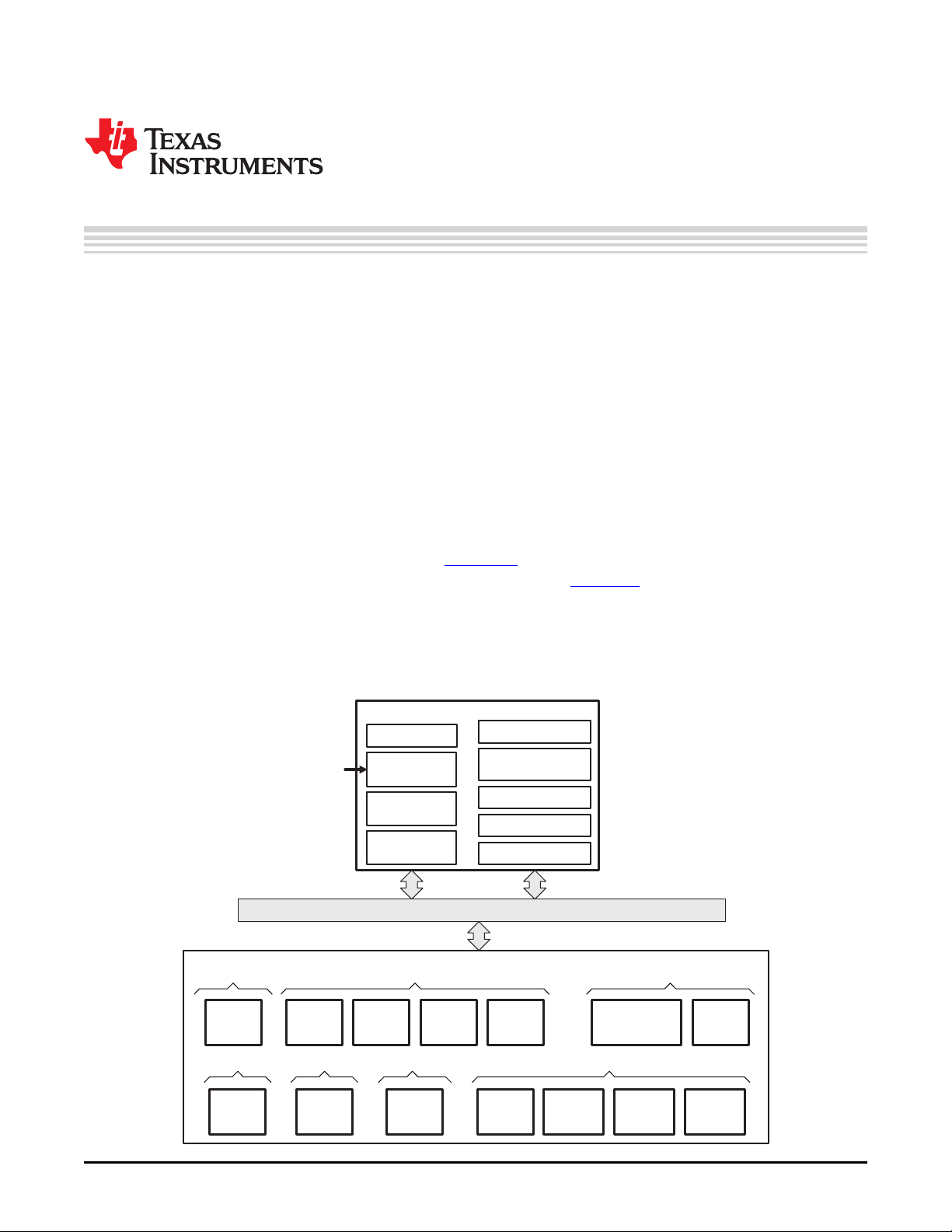
The C5515 DSP block diagram is shown in Figure 1-1 .
Figure 1-1. Functional Block Diagram
SPRUFX5A–October 2010–Revised November 2010 System Control
Submit Documentation Feedback
Copyright © 2010, Texas Instruments Incorporated
13
Page 14

Introduction
1.1.2 CPU Core
The C55x CPU is responsible for performing the digital signal processing tasks required by the
application. In addition, the CPU acts as the overall system controller, responsible for handling many
system functions such as system-level initialization, configuration, user interface, user command
execution, connectivity functions, and overall system control.
Tightly coupled to the CPU are the following components:
• DSP internal memories
– Dual-access RAM (DARAM)
– Single-access RAM (SARAM)
– Read-only memory (ROM)
• FFT hardware accelerator
• Ports and buses
The CPU also manages/controls all peripherals on the device. Refer to the device-specific data manual for
the full list of peripherals.
Figure 1-1 shows the functional block diagram of the DSP and how it connects to the rest of the device.
The DSP architecture uses the switched central resource (SCR) to transfer data within the system.
1.1.3 FFT Hardware Accelerator
The C55x CPU includes a tightly-coupled FFT hardware accelerator that communicates with the C55x
CPU through the use coprocessor instructions. For ease of use, the ROM has a set of C-callable routines
that use these coprocessor instructions to perform 8, 16, 32, 64, 128, or 256-point FFTs. The main
features of the FFT hardware accelerator are:
• Support for 8 to 1024-point (in powers of 2) real and complex-valued FFTs and IFFTs.
• An internal twiddle factor generator for optimal use of memory bandwidth and more efficient
programming.
• Basic and software-driven auto-scaling feature provides good precision vs cycle count trade-off.
• Single-stage and double-stage modes enabling computation of one or two stages in one pass, thus
handling odd power of two FFT widths.
www.ti.com
1.1.3.1 Using FFT Accelerator ROM routines
The C5505 includes C-callable routines in ROM to execute FFT and IFFT using the tightly coupled FFT
accelerator. The routines reside in the following address:
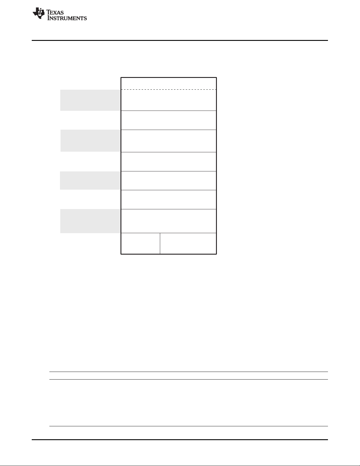
Table 1-1.
Address Name Description Calling Convention
0x00ff6cd6 hwafft br Vector bit-reversal void hwafft_br( Int32 *data, Int32 *data_br, Uint16
0x00ff6cea hwafft 8pts 8-pt FFT/IFFT Uint16 hwafft_8pts( Int32 *data,Int32 *scratch, Uint16
0x00ff6dd9 hwafft 16pts 16-pt FFT/IFFT Uint16 hwafft_16pts( Int32 *data,Int32 *scratch, Uint16
0x00ff6f2f hwafft 32pts 32-pt FFT/IFFT Uint16 hwafft_32pts( Int32 *data,Int32 *scratch, Uint16
0x00ff7238 hwafft 64pts 64-pt FFT/iFFT Uint16 hwafft_64pts( Int32 *data,Int32 *scratch, Uint16
0x00ff73cd hwafft 128pts 128-pt FFT/IFFT Uint16 hwafft_128pts( Int32 *data,Int32 *scratch,
0x00ff75de hwafft 256pts 256-pt FFT/IFFT Uint16 hwafft_256pts( Int32 *data,Int32 *scratch,
0x00ff77dc hwafft 512pts 512-pt FFT/iFFT Uint16 hwafft_512pts( Int32 *data,Int32 *scratch,
0x00ff7a56 hwafft 1024pts 1024-pt FFT/IFFT Uint16 hwafft_1024pts( Int32 *data,Int32 *scratch,
14
System Control SPRUFX5A–October 2010–Revised November 2010
Copyright © 2010, Texas Instruments Incorporated
data_len );
fft_flag, Uint16 scale_flag);
fft_flag, Uint16 scale_flag);
fft_flag, Uint16 scale_flag);
fft_flag, Uint16 scale_flag);
Uint16 fft_flag, Uint16 scale_flag);
Uint16 fft_flag, Uint16 scale_flag);
Uint16 fft_flag, Uint16 scale_flag);
Uint16 fft_flag, Uint16 scale_flag);
Submit Documentation Feedback
Page 15

www.ti.com
Note that for the FFT routines, output data is dependent on the return value (T0). If return = 0 output data
is in-place, meaning the result will overwrite the input buffer. If return =1, output data is placed in the
scratch buffer. The 32-bit input and output data consist of 16-bit real and 16-bit imaginary data. If only real
data is used, the imaginary part can be zeroed. The Scale flag determines if the butterfly output is divided
by 2 to prevent overflow at the expense of resolution. For further information on how to use these routines,
see FFT Implementation on the TMS320VC5505, TMS320C5505, and TMS320C5515 DSPs (SPRABB6).
1.1.4 Power Management
Integrated into the C5515/14 DSP are the following power management features:
• One low dropout LDO for analog portions of the device, DSP PLL (V
management circuits (V
• One LDO for DSP core (CVDD): DSP_LDO
• One LDO for USB core and PHY (USB_V
• Idle controller with several clock domains:
– CPU domain
– Clock generator domain
– Peripheral domain
– USB domain
– Real-time clock (RTC) domain
• Independent voltage and power domains
• LDOI (LDOs and Bandgap Power Supply)
• Analog POR, SAR, and PLL (V
• Real-time clock core (CV
• Digital core (CVDD)
• USB core (USB_ V
• USB PHY and USB PLL (USB_V
• EMIF I/O (DV
• RTC I/O (DV
• Rest of the I/O (DV
DDEMIF
DDRTC
)
)
DDA_ANA
and USB_V
DD1P3
)
DDIO
): ANA_LDO
)
DDRTC
DDA_ANA
DDOSC
and V
DDA1P3
, USB_V
DDA1P3
DDA_PLL
)
): USB_LDO
)
, and USB_V
DDA3P3
DDPLL
), SAR, and power
DDA_PLL
)
Introduction
1.1.5 Peripherals
The DSP includes the following peripherals:
• Four direct memory access (DMA) controllers, each with four independent channels.
• One external memory interface (EMIF) with 21-bit address and 16-bit data. The EMIF has support for
mobile SDRAM and non-mobile SDRAM single-level cell (SCL) NAND with 1-bit ECC, and multi-level
cell (MLC) NAND with 4-bit ECC.
NOTE: The C5515 can support non-mobile SDRAM under certain circumstances. The C5515
always uses mobile SDRAM initialization but it is able to support SDRAM memories that
ignore the BA0 and BA1 pins for the 'load mode register' command. During the mobile
SDRAM initialization, the device issues the 'load mode register' initialization command to two
different addresses that differ in only the BA0 and BA1 address bits. These registers are the
Extended Mode register and the Mode register. The Extended mode register exists only in
mSDRAM and not in non-mSDRAM. If a non-mobile SDRAM memory ignores bits BA0 and
BA1, the second loaded register value overwrites the first, leaving the desired value in the
Mode register and the non-mobile SDRAM will work with C5515.
• Two serial busses each configurable to support one Multimedia Card (MMC) / Secure Digital
(SD/SDIO) controller, one inter-IC sound bus (I2S) interface with GPIO, or a full GPIO interface.
• One parallel bus configurable to support a 16-bit LCD bridge or a combination of an 8-bit LCD bridge,
a serial peripheral interface (SPI), an I2S, a universal asynchronous receiver/transmitter (UART), and
GPIO.
• One inter-integrated circuit (I2C) multi-master and slave interface with 7-bit and 10-bit addressing
SPRUFX5A–October 2010–Revised November 2010 System Control
Submit Documentation Feedback
Copyright © 2010, Texas Instruments Incorporated
15
Page 16

System Memory
modes.
• Three 32-bit timers with 16-bit prescaler; one timer supports watchdog functionality.
• A USB 2.0 slave.
• A 10-bit successive approximation (SAR) analog-to-digital converter with touchscreen conversion
capability.
• One real-time clock (RTC) with associated low power mode.
1.2 System Memory
The DSP supports a unified memory map (program code sections and data sections can be mixed and
interleaved within the entire memory space) composed of both on-chip and external memory. The on-chip
memory consists of 320KB of RAM and 128KB of ROM.
The external memory interface (EMIF) port provides the means for the DSP to access external memory
and devices including: mobile and non-mobile single data rate (SDR) SDRAM, (for limitations, see note in
Section 1.1.5), NOR Flash, NAND Flash and SRAM.
Separate from the program and data space, the DSP also includes a 64K-byte I/O space for peripheral
registers.
1.2.1 Program/Data Memory Map
The device provides 16MB of total address space composed of on-chip RAM, on-chip ROM, and external
memory space supporting a variety of memory types. The on-chip, dual-access RAM allows two accesses
to a given block during the same cycle. The device has 8 blocks of 8K-bytes of dual-access RAM. The
on-chip, single-access RAM allows one access to a given block per cycle. The device has 32 blocks of
8K-bytes of single-access RAM. Attempts to perform two accesses in a cycle to single-access memory will
cause one access to stall until the next cycle. An access is defined as either a read or write operation. For
the most efficient use of DSP processing power (MIPS), it is important to pay attention to the memory
blocks that are being simultaneously accessed by the code and data operations.
The external memory space is divided into five spaces. Each space has a chip select decode signal
(called CS) that indicates an access to the selected space. The external memory interface (EMIF)
supports access to asynchronous memories such as SRAM Flash, mobile SDRAM and SDRAM.
www.ti.com
The DSP memory is accessible by different master modules within the DSP, including the device CPU, the
four DMA controllers, and the USB. The DSP memory map as seen by these modules is illustrated in
Figure 1-2.
16
System Control SPRUFX5A–October 2010–Revised November 2010
Submit Documentation Feedback
Copyright © 2010, Texas Instruments Incorporated
Page 17
0001 0000h
64K Minus 192 Bytes
DARAM
(D)
0009 0000h
SARAM
256K Bytes
External-CS2 Space
(C)
0200 0000h
0300 0000h
0400 0000h
0500 0000h
050E 0000h
128K Bytes Asynchronous (if MPNMC=1)
128K Bytes ROM (if MPNMC=0)
External-CS3 Space
(C)
External-CS4 Space
(C)
External-CS5 Space
(C)
BLOCK SIZE
DMA/USB/LCD
BYTE ADDRESS
(A)
ROM
(if MPNMC=0)
External-CS5
f MPNMC=1)
(C)
Space
(i
1M Minus 128K Bytes Asynchronous
1M Bytes Asynchronous
2M Bytes Asynchronous
4M Bytes Asynchronous
MEMORY BLOCKS
0001 00C0h
MMR (Reserved)
(B)
0100 0000h
External-CS0 Space
(C)(E)
8M Minus 320K Bytes SDRAM/mSDRAM
050F FFFFh
000000h
010000h
800000h
C00000h
E00000h
F00000h
FE0000h
CPU BYTE
ADDRESS
(A)
0000C0h
050000h
FFFFFFh
www.ti.com
System Memory
Figure 1-2. DSP Memory Map
A Address shown represents the first byte address in each block.
B The first 192 bytes are reserved for memory-mapped registers (MMRs).
C Out of the four DMA controllers, only DMA controller 3 has access to the external memory space.
D The USB controller does not have access to DARAM.
E The CS0 space can be accessed by CS0 only or by CS0 and CS1.
1.2.1.1 On-Chip Dual-Access RAM (DARAM)
The DARAM is located in the CPU byte address range 00 00C0h - 00 FFFFh and is composed of eight
blocks of 4K words each (see Table 1-2). Each DARAM block can perform two accesses per cycle (two
reads, two writes, or a read and a write). DARAM can be accessed by the internal program, data, and
DMA buses.
As shown in Table 1-2, the DMA controllers access DARAM at an address offset 0x0001_0000 from the
CPU memory byte address space.
(1)
First 192 bytes are reserved for memory-mapped registers (MMRs).
Memory Block CPU Byte Address Range DMA/USB Controller Byte Address Range
DARAM 0
DARAM 1 00 2000h - 00 3FFFh 0001 2000h - 0001 3FFFh
(1)
DARAM 2 00 4000h - 00 5FFFh 0001 4000h - 0001 5FFFh
DARAM 3 00 6000h - 00 7FFFh 0001 6000h - 0001 7FFFh
DARAM 4 00 8000h - 00 9FFFh 0001 8000h - 0001 9FFFh
DARAM 5 00 A000h - 00 BFFFh 0001 A000h - 0001 BFFFh
Table 1-2. DARAM Blocks
00 00C0h - 00 1FFFh 0001 00C0h - 0001 1FFFh
SPRUFX5A–October 2010–Revised November 2010 System Control
Submit Documentation Feedback
Copyright © 2010, Texas Instruments Incorporated
17
Page 18

System Memory
Table 1-2. DARAM Blocks (continued)
Memory Block CPU Byte Address Range DMA/USB Controller Byte Address Range
DARAM 6 00 C000h - 00 DFFFh 0001 C000h - 0001 DFFFh
DARAM 7 00 E000h - 00 FFFFh 0001 E000h - 0001 FFFFh
1.2.1.2 On-Chip Single-Access RAM (SARAM)
The SARAM is located at the CPU byte address range 01 0000h - 04FFFFh and is composed of 32 blocks
of 4K words each (see Table 1-3). Each SARAM block can perform one access per cycle (one read or one
write). SARAM can be accessed by the internal program, data, and DMA buses.
As shown in Table 1-3, the DMA controllers access SARAM at an address offset 0x0008_0000 from the
CPU memory byte address space.
Table 1-3. SARAM Blocks
Memory Block CPU Byte Address Range Range
SARAM 0 01 0000h - 01 1FFFh 0009 0000h - 0009 1FFFh
SARAM 1 01 2000h - 01 3FFFh 0009 2000h - 0009 3FFFh
SARAM 2 01 4000h - 01 5FFFh 0009 4000h - 0009 5FFFh
SARAM 3 01 6000h - 01 7FFFh 0009 6000h - 0009 7FFFh
SARAM 4 01 8000h - 01 9FFFh 0009 8000h - 0009 9FFFh
SARAM 5 01 A000h - 01 BFFFh 0009 A000h - 0009 BFFFh
SARAM 6 01 C000h - 01 DFFFh 0009 C000h - 0009 DFFFh
SARAM 7 01 E000h - 01 FFFFh 0009 E000h - 0009 FFFFh
SARAM 8 02 0000h - 02 1FFFh 000A 0000h - 000A 1FFFh
SARAM 9 02 2000h - 02 3FFFh 000A 2000h - 000A 3FFFh
SARAM 10 02 4000h - 02 5FFFh 000A 4000h - 000A 5FFFh
SARAM 11 02 6000h - 02 7FFFh 000A 6000h - 000A 7FFFh
SARAM 12 02 8000h - 02 9FFFh 000A 8000h - 000A 9FFFh
SARAM 13 02 A000h - 02 BFFFh 000A A000h - 000A BFFFh
SARAM 14 02 C000h - 02 DFFFh 000A C000h - 000A DFFFh
SARAM 15 02 E000h - 02 FFFFh 000A E000h - 000A FFFFh
SARAM 16 03 0000h - 03 1FFFh 000B 0000h - 000B 1FFFh
SARAM 17 03 2000h - 03 3FFFh 000B 2000h - 000B 3FFFh
SARAM 18 03 4000h - 03 5FFFh 000B 4000h - 000B 5FFFh
SARAM 19 03 6000h - 03 7FFFh 000B 6000h - 000B 7FFFh
SARAM 20 03 8000h - 03 9FFFh 000B 8000h - 000B 9FFFh
SARAM 21 03 A000h - 03 BFFFh 000B A000h - 000B BFFFh
SARAM 22 03 C000h - 03 DFFFh 000B C000h - 000B DFFFh
SARAM 23 03 E000h - 03 FFFFh 000B E000h - 000B FFFFh
SARAM 24 04 0000h - 04 1FFFh 000C 0000h - 000C 1FFFh
SARAM 25 04 2000h - 04 3FFFh 000C 2000h - 000C 3FFFh
SARAM 26 04 4000h - 04 5FFFh 000C 4000h - 000C 5FFFh
SARAM 27 04 6000h - 04 7FFFh 000C 6000h - 000C 7FFFh
SARAM 28 04 8000h - 04 9FFFh 000C 8000h - 000C 9FFFh
SARAM 29 04 A000h - 04 BFFFh 000C A000h - 000C BFFFh
SARAM 30 04 C000h - 04 DFFFh 000C C000h - 000C DFFFh
SARAM 31 04 E000h - 04 FFFFh 000C E000h - 000C FFFFh
www.ti.com
DMA/USB Controller Byte Address
18
System Control SPRUFX5A–October 2010–Revised November 2010
Copyright © 2010, Texas Instruments Incorporated
Submit Documentation Feedback
Page 19

www.ti.com
1.2.1.3 On-Chip Single-Access Read-Only Memory (SAROM)
The zero-wait-state ROM is located at the CPU byte address range FE 0000h - FF FFFFh. The ROM is
composed of four 16K-word blocks, for a total of 128K-bytes of ROM. Each ROM block can perform one
access per cycle (one read or one write). ROM can be accessed by the internal program or data buses,
but not the DMA buses. The ROM address space can be mapped by software to the external memory or
to the internal ROM via the MPNMC bit in the ST3 status register.
The standard device includes a Bootloader program resident in the ROM and the bootloader code is
executed immediately after hardware reset. When the MPNMC bit field of the ST3 status register is set
through software, the on-chip ROM is disabled and not present in the memory map, and byte address
range FE 0000h - FF FFFFh is directed to external memory space (extends CS5 address reach). A
hardware reset always clears the MPNMC bit, so it is not possible to disable the ROM at hardware reset.
However, the software reset instruction does not affect the MPNMC bit. The ROM can be accessed by the
program and data buses. Each SAROM block can perform one word read access per cycle.
Table 1-4. SAROM Blocks
Memory Block CPU Byte Address Range CPU Word Address Range
SAROM0 FE 0000h - FE 7FFFh 7F 0000h - 7F 3FFFh
SAROM1 FE 8000h - FE FFFFh 7F 4000h - 7F 7FFFh
SAROM2 FF 0000h - FF 7FFFh 7F 8000h - 7F BFFFh
SAROM3 FF 8000h - FF FFFFh 7F C000h - 7F FFFFh
1.2.1.4 External Memory
The external memory space of the device is located at the byte address range 05 0000h - FF FFFFh. The
external memory space is divided into five chip select spaces. The synchronous space is activated by one
chip select pin (EM_CS0) or by a pair of chip selects pins (EM_CS0 and EM_CS1). Each asynchronous
chip select space has a corresponding chip select pin (called EMIF_CS[2:5]) that is activated during an
access to the chip select space.
The external memory interface (EMIF) provides the means for the DSP to access external memories and
other devices including: NOR Flash, NAND Flash, SRAM, mSDRAM, and SDRAM (see section 1.5 for
limitations). Before accessing external memory, you must configure the EMIF through its registers. For
more detail on the EMIF, see the TMS320C5515/14/05/04 DSP External Memory Interface (EMIF) User’s
Guide (SPRUGU6).
As described in Section 1.2.1.3, when the MPNMC bit field of the ST3 status register is cleared (default),
the byte address range FE 0000h - FF FFFFh is reserved for the on-chip ROM, which decreases the
addressable size for EM_CS5.
The EMIF provides a configurable 16-bit (synchronous or asynchronous) or 8-bit (asynchronous only) data
bus, an address bus width of up to 21-bits, and five dedicated chip selects, along with memory control
signals. To maximize power savings, the I/O pins of the EMIF can be operated at lower voltage
independently of other I/O pins on the DSP. Further power savings may be achieved by setting the EMIF
I/O pins to have slow slew rate, as described in Section 1.7.3.4.
System Memory
1.2.1.4.1 Asynchronous EMIF Interface
The EMIF provides a configurable 16- or 8-bit data bus with address bus width of up to 21-bits, and six
dedicated chip selects, along with memory control signals. The cycle timings of the asynchronous
interface are fully programmable, allowing for access to a wide range of devices including NAND flash,
NOR flash, and SRAM as well as other asynchronous devices such as a TI DSP HPI interface. In NAND
mode, the asynchronous interface supports 1-bit ECC for 8- and 16-bit NAND flash and 4-bit ECC for 8-bit
NAND flash.
1.2.1.5 Synchronous EMIF Interface
The EMIF provides a 16-bit data bus with one or two dedicated chip selects for mSDRAM. Non-mobile
SDRAM can be supported under certain circumstances. The C5515 always uses a mobile SDRAM
initialization command sequence, but it is able to support SDRAM memories that ignore the BA0 and BA1
SPRUFX5A–October 2010–Revised November 2010 System Control
Submit Documentation Feedback
Copyright © 2010, Texas Instruments Incorporated
19
Page 20

Device Clocking
pins for the load mode register command. During the mobile SDRAM initialization, the device issues the
load mode register initialization command to two different addresses that differ in only the BA0 and BA1
address bits. These registers are the Extended Mode register and the Mode register. The extended mode
register exists only in mSDRAM, and not in non-mSDRAM. If a non-mobile SDRAM memory ignores bits
BA0 and BA1, the second loaded register value overwrites the first, leaving the desired value in the mode
register and the non-mobile SDRAM works with the device.
Some timing parameters are programmable such as the refresh rate and CAS latencies. The EMIF
supports up to 100 MHz SDCLK and has the ability to run the SDCLK at half the system clock to meet the
EMIF I/O timing requirements and/or at lower power if a slower SDCLK can be used. Detailed information
is available in the Clock Control section of the TMS320C5515/14/05/04 DSP External Memory Interface
(EMIF) User's Guide (SPRUGU6).
1.2.2 I/O Memory Map
The C5x DSP has a separate memory map for peripheral and system registers, called I/O space. This
space is 64K-words in length and is accessed via word read and write instructions dedicated for I/O
space.
Separate documentation for I/O space registers related to each peripheral exists and is listed in the
preface of this guide. System registers, which provide system-level control and status, are described in
detail in other sections throughout this guide. Unused addresses in I/O space should be treated as
reserved and should not be accessed. Accessing unused I/O space addresses may stall or hang the DSP.
Each of the four DMA controllers has access to a different set of peripherals and their I/O space registers.
This is shown in Section 1.7.4.
www.ti.com
NOTE: Writting to I/O space registers incurs in at least 2 CPU cycle latency. Thus, when
configuring peripheral devices, wait at least two cycles before accessing data from the
peripheral. When more than one peripheral register is updated in a sequence, the CPU only
needs to wait following the final register write. For example, if the EMIF is being
reconfigured, the CPU must wait until the very last EMIF register update takes effect before
trying to access the external memory. The users should consult the respective peripheral
user's guide to determine if a peripheral requires additional initialization time.
Before accessing any peripheral register, make sure the peripheral is not held in reset and its internal
clock is enabled. The peripheral reset control register (Section 1.7.5.2) and the peripheral clock gating
control registers (Section 1.5.3.2.1) control these functions. Accessing a peripheral whose clocks are
gated will either return the value of the last address read from the peripheral (when the clocks were last
ON) or it may possibly hang the DSP -- depending on the peripheral.
1.3 Device Clocking
1.3.1 Overview
The DSP requires two primary reference clocks: a system reference clock and a USB reference clock. The
system clock, which is used by the CPU and most of the DSP peripherals, is controlled by the system
clock generator. The system clock generator features a software-programmable PLL multiplier and several
dividers. The system clock generator accepts an input reference clock from the CLKIN pin or the output
clock of the 32.768-KHz real-time clock (RTC) oscillator. The selection of the input reference clock is
based on the state of the CLK_SEL pin. The CLK_SEL pin is required to be statically tied high or low and
cannot change dynamically after reset. The system clock generator can be used to modify the system
reference clock signal according to software-programmable multiplier and dividers. The resulting clock
output, the DSP system clock, is passed to the CPU, peripherals, and other modules inside the DSP.
Alternatively, the system clock generator can be fully bypassed and the input reference clock can be
passed directly to the DSP system clock. The USB reference clock is generated using a dedicated on-chip
oscillator with a 12 MHz external crystal connected to the USB_MXI and USB_MXO pins. This crystal is
not required if the USB peripheral is not being used. The USB oscillator cannot be used to provide the
system reference clock.
The RTC oscillator generates a clock when a 32.768-KHz crystal is connected to the RTC_XI and
20
System Control SPRUFX5A–October 2010–Revised November 2010
Submit Documentation Feedback
Copyright © 2010, Texas Instruments Incorporated
Page 21

www.ti.com
Device Clocking
RTC_XO pins. RTC core (CV
) must be powered all the time but the 32.768-KHz crystal can be
DDRTC
disabled if CLKIN is used as the clock source for the DSP. However, when the RTC oscillator is disabled,
the RTC peripheral will not operate and the RTC registers (I/O address range 1900h - 197Fh) will not be
accessible. This includes the RTC power management register (RTCPMGT) which controls the
RTCLKOUT and WAKEUP pins. To disable the RTC oscillator, connect the RTC_XI pin to CV
DDRTC
and
the RTC_XO pin to ground.
The USB oscillator is powered down at hardware reset. It must be enabled (by the NNN register) and
must be allowed to settle for an amount of time specified by USB Oscillator Startup Time parameter in the
device specific manual before using the USB peripheral.
Figure 1-3 shows the overall DSP clock structure. For detailed specifications on clock frequency, voltage
requirements, and oscillator/crystal requirements, see the device-specific data manual.
SPRUFX5A–October 2010–Revised November 2010 System Control
Submit Documentation Feedback
Copyright © 2010, Texas Instruments Incorporated
21
Page 22
CLKSEL
1
0
CLKIN
PCGCR1
[SYSCLKDIS]
LS
1
0
LS
CCR2
[SYSCLKSEL]
SYSCLK
System Clock
Generator
ST3_55[CLKOFF]
CLKOUT
ICR[HWAI]
FFT Hardware
ICR[MPORTI]
MPORT Clock
ICR[XPORTI]
XPORT Clock
PCGCR2[DMA1CG]
DMA0
PCGCR2[DMA2CG]
DMA1
PCGCR2[DMA3CG]
DMA2
DMA3
ICR[IPORTI]
IPORT Clock
ICR[DPORTI]
DPORT Clock
ICR[CPUI]
CPU Clock
PCGCR1[EMIFCG]
÷2
0
1
ECDR[EDIV]
EMIF
PCGCR2[USBCG]
LS
USB
Digital
USB
OSC
USB_MXI
UDB_MXO
12 MHz
USBSCR
[USBOSCDIS]
PCGCR1[DMA0CG]
PCGCR1[SPICG]
SPI
PCGCR1[UARTCG]
I2C
PCGCR1[TMR2CG]
UART
PCGCR1[TMR1CG]
Timer2
Timer1
PCGCR1[I2CCG]
PCGCR1[TMR0CG]
Timer0
PCGCR1[I2S0CG]
I2S0
PCGCR1[I2S1CG]
I2S1
PCGCR1[I2S2CG]
I2S2
PCGCR1[I2S3CG]
I2S3
PCGCR2[SARCG]
SAR
PCGCR2[LCDCG]
LCD Controller
PCGCR1[MMCSD0CG]
MMC/SD0
PCGCR1[MMCSD1CG]
MMC/SD1
USBPHYCLK
RTC Clock
LS
RTC
OSC
RTC_XI
RTC_XO
32.768
KHz
RTC_CLKOUT
RTC
LS
CLKREF
(1)
(1) (1)
(1)
(2)
Accelerator
USB
PHY
60 MHz
USB
PLL
OFF
12 MHz
PCGCR2[ANAREGCG]
Analog
Registers
(1)
Device Clocking
22
www.ti.com
Figure 1-3. DSP Clocking Diagram
(1) LS = Level Shifter
(2) The CLKOUT pin's output driver is enabled/disabled through the CLKOFF bit of the CPU ST3_55 register. At
the beginning of the boot sequence, the on-chip Bootloader sets CLKOFF = 1 and CLKOUT pin is disabled
(high-impedance). For more information on the ST3_55 register, see the TMS320C55x 3.0 CPU Reference
Guide (SWPU073).
System Control SPRUFX5A–October 2010–Revised November 2010
Copyright © 2010, Texas Instruments Incorporated
Submit Documentation Feedback
Page 23

www.ti.com
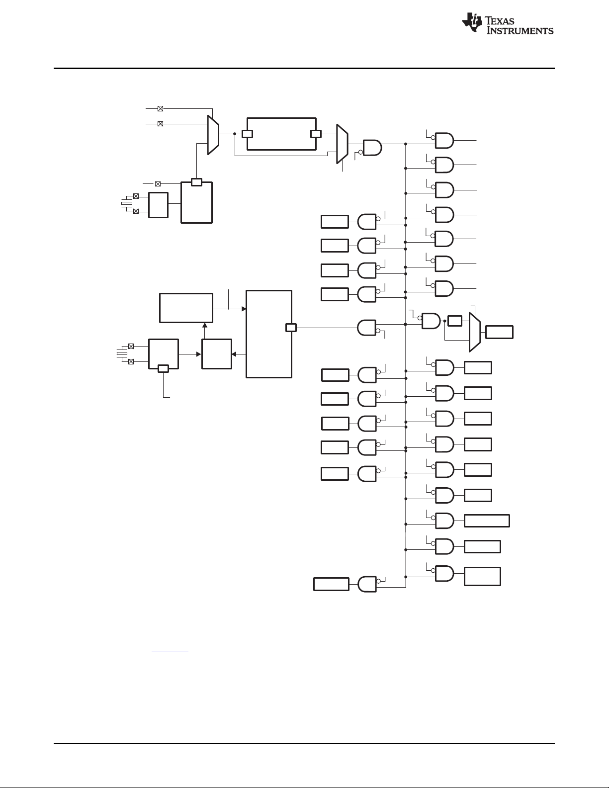
1.3.2 Clock Domains
The device has many clock domains defined by individually disabled portions of the clock tree structure.
Understanding the clock domains and their clock enable/disable control registers is very important for
managing power and for ensuring clocks are enabled for domains that are needed. By disabling the clocks
and thus the switching current in portions of the chip that are not used, lower dynamic power consumption
can be achieved and prolonging battery life.
Figure 1-3 shows the clock tree structure with the clock gating represented by the AND gates. Each AND
gate shows the controlling register that allows the downstream clock signal to be enabled/disabled. Once
disabled most clock domains can be re-enabled, when the associated clock domain logic is needed, via
software running on the CPU. But some domains actually stop the clocks to the CPU and therefore
software running on the CPU cannot be responsible for re-enabling those clock domains. Other
mechanism must exist for restarting those clocks, and the specific cases are listed below:
• The System Clock Generator (PLL) can be powered-down by writing a 1 to PLL_PWRDN bit in the
clock generator control register CGCR1. This stops the PLL from oscillating and shuts down its analog
circuits. It is important to bypass the System Clock Generator by writing 0 to SYSCLKSEL bit in CCR2
(clock confguration register 2) prior to powering it down, else the CPU will loose its clock and not be
able to recover without hardware reset.
NOTE: Failsafe logic exists to prevent selecting the PLL clock if it has been powered down but this
logic does not protect against powering down the PLL while it is selected as the system clock
source. Therefore, software should always maintain responsibility for bypassing the PLL prior
to and whenever it is powered down.
System Clock Generator
• The SYSCLKDIS bit in PCGCR1 [clock gating control register 1) is the master clock gater. Asserting
this bit causes the main system clock, SYSCLK, to stop and, therefore, the CPU and all peripherals no
longer receive clocks. The WAKEUP pin, INT0 & INT1 pin, or RTC interrupt can be used to re-enable
the clock from this condition.
• The ICR bit in CPUI(clock gating control register) gates clocks to the CPU and uses the CPU’s idle
instruction to initiate the clock off mode. Any non-masked interrupt can be used to re-enable the CPU
clocks.
1.4 System Clock Generator
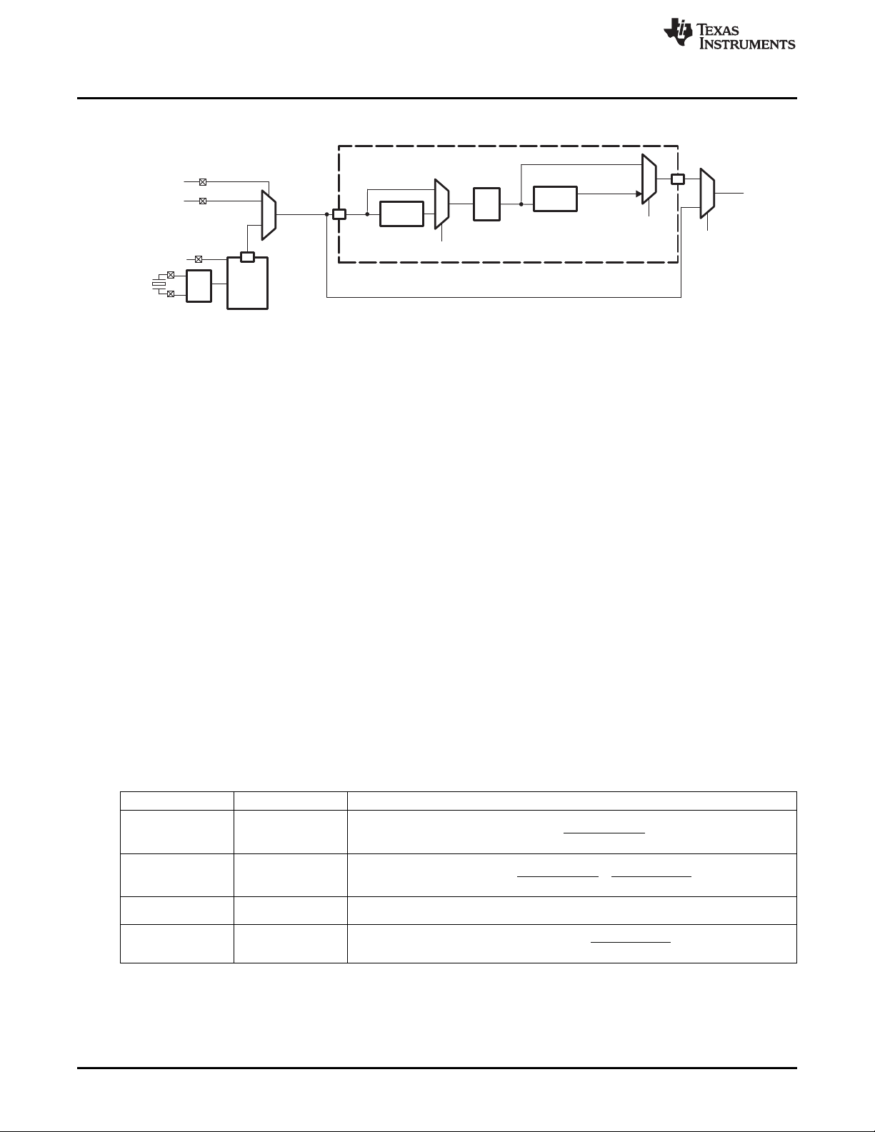
1.4.1 Overview
The system clock generator (Figure 1-4) features a software-programmable PLL multiplier and several
dividers. The clock generator accepts an input clock from the CLKIN pin or the output clock of the
real-time clock (RTC) oscillator. The clock generator offers flexibility and convenience by way of
software-configurable multiplier and divider to modify the clock rate internally. The resulting clock output,
SYSCLK, is passed to the CPU, peripherals, and other modules inside the DSP.
A set of registers are provided for controlling and monitoring the activity of the clock generator. You can
write to the SYSCLKSEL bit in CCR2 register to toggle between the two main modes of operation:
• In the BYPASS MODE (see Section 1.4.3.1), the entire clock generator is bypassed, and the frequency
of SYSCLK is determined by CLKIN or the RTC oscillator output. Once the PLL is bypassed, the PLL
can be powered down to save power.
• In the PLL MODE (see Section 1.4.3.2), the input frequency can be both multiplied and divided to
produce the desired SYSCLK frequency, and the SYSCLK signal is phase-locked to the input clock
signal (CLKREF).
The clock generator bypass mux (controlled by SYSCLKSEL bit in CCR2 register) is a glitchfree mux,
which means that clocks will be switched cleanly and not short cycle pulses when switching among the
BYPASS MODE and PLL MODE.
For debug purposes, the CLKOUT pin can be used to see different clocks within the clock generator. For
details, see Section 1.4.2.3.
SPRUFX5A–October 2010–Revised November 2010 System Control
Submit Documentation Feedback
Copyright © 2010, Texas Instruments Incorporated
23
Page 24
CLKREF
Reference
Divider
1
0
CGCR2[RDBYPASS]
PLL
LS
PLLIN
PLLOUT
Output
Divider
0
CGCR4.
[OUTDIVEN]
1
0
CCR2.
[SYSCLKSEL]
LS
SYSCLK
CLKSEL
1
0
CLKIN
RTC Clock
LS
RTC
OSC
RTC_XI
RTC_XO
32.768
KHz
RTC_CLKOUT
RTC
1
( )
M + 4
CLKREF
RDRATIO + 4
´
( )
M + 4
1
CLKREF
RDRATIO + 4 ODRATIO + 1
´ ´
CLKREF
M + 4
´
é ù
ë û
1
CLKREF
M + 4
ODRATIO + 1
´ ´
é ù
ë û
System Clock Generator
1.4.2 Functional Description
The following sections describe the multiplier and dividers of the clock generator.
1.4.2.1 Multiplier and Dividers
The clock generator has a one multiplier and a two programmable dividers: one before the PLL input and
one on the PLL output. The PLL can be programmed to multiply the PLL input clock, PLLIN, using a x4 to
x4099 multiplier value. The reference clock divider can be programmed to divide the clock generator input
clock from a /4 to /4099 divider ratio and may be bypassed. The Reference Divider and RDBYPASS mux
must be programmed such that the PLLIN frequency range is 32.786 KHz to 170 KHz. At the output of the
PLL, the output divider can be used to divide the PLL output clock, PLLOUT, from a /1 to a /128 divider
ratio and may also be bypassed. The PLL output, PLLOUT, frequency must be programmed within the
range of at least 60 MHz and no more than the maximum operating frequency defined by the datasheet,
Fsysclk_max parameter. See Table 1-10 for allowed values of PLLIN, PLLOUT, and SYSCLK. Keep in
mind that programming the output divider with an odd divisor value other than 1 will result in a non-50%
duty cycle SYSCLK. This is not a problem for any of the on-chip logic, but the non-50% duty cycle will be
visible on chip pins such as EM_SDCLK (in full-rate mode) and CLKOUT. See Table 1-10 for allowed
values of PLLIN, PLLOUT, and SYSCLK.
www.ti.com
Figure 1-4. Clock Generator
The multiplier and divider ratios are controlled through the PLL control registers. The M bits define the
multiplier rate. The RDRATIO and ODRATIO bits define the divide ratio of the reference divider and
programmable output divider, respectively. The RDBYPASS and OUTDIVEN bits are used to enable or
bypass the dividers. Table 1-5 lists the formulas for the output frequency based on the setting of these
bits.
The clock generator must be placed in BYPASS MODE when any PLL dividers or multipliers are changed.
Then, it must remain in BYPASS MODE for at least 4 mS before switching to PLL MODE.
Table 1-5. PLL Output Frequency Configuration
RDBYPASS OUTDIVEN SYSCLK Frequency
0 0
0 1
1 0
1 1
1.4.2.2 Powering Down and Powering Up the System PLL
24
To save power, you can put the PLL in its power down mode. You can power down the PLL by setting the
PLL_PWRDN = 1 in the clock generator control register CGCR1. However, before powering down the
PLL, you must first place the clock generator in bypass mode.
System Control SPRUFX5A–October 2010–Revised November 2010
Copyright © 2010, Texas Instruments Incorporated
Submit Documentation Feedback
Page 25

www.ti.com
System Clock Generator
When the PLL is powered up (PLL_PWRDN = 0), the PLL will start its phase-locking sequence. You must
keep the clock generator in BYPASS MODE for at least 4 mS while the phase-locking sequence is
ongoing. See Section 1.4.3.2 for more details on the PLL_MODE of the clock generator.
1.4.2.3 CLKOUT Pin
For debug purposes, the DSP includes a CLKOUT pin which can be used to tap different clocks within the
clock generator. The SRC bits of the CLKOUT control source register (CCSSR) can be used to specify the
source for the CLKOUT pin (see Figure 1-5 and Table 1-6).
NOTE: There is no internal logic to prevent glitches while changing the CLKOUT source. Also there
is no provision for internally dividing down the CLKOUT frequency other than the options
inherently available for selecting the CLKOUT source.
The CLKOUT pin's output driver is enabled/disabled through the CLKOFF bit of the CPU ST3_55 register.
At hardware reset, CLKOFF is cleared to 0 so that the clock is visible for debug purposes. But within the
bootloader romcode, CLKOFF is set to 1 to conserve power. After the bootloader finishes, the customer
application code is free to re-enable CLKOUT. For more information on the ST3_55 register, see the
TMS320C55x 3.0 CPU Reference Guide (SWPU073).
The slew rate (i.e., dV/dt) of the CLKOUT pin can be controlled by the CLKOUTSR bits in the output slew
rate control register (OSRCR). This feature allows for additional power savings when the CLKOUT pin
does not need to drive large loads.
Figure 1-5. CLKOUT Control Source Select Register (CCSSR) [1C24h]
15 4 3 0
Reserved SRC
R-0 R/W-Bh
LEGEND: R/W = Read/Write; R = Read only; -n = value after reset
Table 1-6. CLKOUT Control Source Select Register (CCSSR) Field Descriptions
Bit Field Value Description
15-4 Reserved 0 Reserved.
3-0 SRC CLKOUT source bits. These bits specify the source clock for the CLKOUT pin.
0 CLKOUT pin outputs System PLL output clock, PLLOUT.
1h CLKOUT pin is set high.
2h CLKOUT pin outputs System PLL output clock, PLLOUT.
3h CLKOUT pin is set low.
4h CLKOUT pin outputs System PLL output clock, PLLOUT.
5h CLKOUT pin is set low.
6h CLKOUT pin outputs System PLL output clock, PLLOUT.
7h CLKOUT pin outputs USB PLL output clock.
8h CLKOUT pin outputs System PLL output clock, PLLOUT.
9h CLKOUT pin outputs SAR clock.
Ah CLKOUT pin outputs System PLL output clock, PLLOUT.
Bh CLKOUT pin outputs system clock, SYSCLK (default mode).
Ch CLKOUT pin outputs System PLL output clock, PLLOUT.
Dh Reserved, do not use.
Eh CLKOUT pin outputs System PLL output clock, PLLOUT.
Fh CLKOUT pin outputs USB PLL output clock.
SPRUFX5A–October 2010–Revised November 2010 System Control
Submit Documentation Feedback
Copyright © 2010, Texas Instruments Incorporated
25
Page 26

System Clock Generator
1.4.2.4 DSP Reset Conditions of the System Clock Generator
The following sections describe the operation of the system clock generator when the DSP is held in reset
state and the DSP is removed from its reset state.
1.4.2.4.1 Clock Generator During Reset
During reset, the PLL_PWRDN bit of the clock generator control register 1 (CGCR1) is set to 1, and the
PLL does not generate an output clock. Furthermore, the SYSCLKSEL bit of the clock configuration
register 2 (CCR2) defaults to 0 (BYPASS MODE), and the system clock (SYSCLK) is driven by either the
CLKIN pin or the real-time clock (RTC). See Section 1.4.3.1 for more information on the bypass mode of
the clock generator.
1.4.2.4.2 Clock Generator After Reset
After reset, the on-chip bootloader programs the system clock generator based on the input clock selected
via the CLK_SEL pin. If CLK_SEL = 0, the bootloader programs the system clock generator and sets the
system clock to 12.288 MHz (multiply the 32.768-kHz RTC oscillator clock by 375). If CLK_SEL = 1, the
bootloader bypasses the system clock generator altogether and the system clock is driven by the CLKIN
pin. In this case, the CLKIN frequency is expected to be 11.2896 MHz, 12.0 MHz, or 12.288 MHz. While
the bootloader tries to boot from the USB , the clock generator is programmed to output approximately 36
MHz.
1.4.3 Configuration
www.ti.com
1.4.3.1 BYPASS MODE
When the system clock generator is in the BYPASS MODE, the clock generator is not used and the
system clock (SYSCLK) is driven by either the CLKIN pin or the real-time clock (RTC).
NOTE: In bypass mode, the PLL is not automatically powered down and will still consume power.
For maximum power savings, the PLL should be placed in its power-down mode. See
Section 1.4.2.2 for more details.
1.4.3.1.1 Entering and Exiting the BYPASS MODE
To enter the bypass mode, write a 0 to the SYSCLKSEL bit in the clock configuration register 2 (CCR2). In
bypass mode, the frequency of the system clock (SYSCLK) is determined by the CLK_SEL pin. If
CLK_SEL = 0, SYSCLK is driven by the output of the RTC. Otherwise, SYSCLK will be driven by the
CLKIN pin.
To exit the BYPASS MODE, ensure the PLL has completed its phase-locking sequence by waiting at least
4 ms and then write a 1 to the SYSCLKSEL bit. The frequency of SYSCLK will then be determined by the
multiplier and divider ratios of the PLL System Clock Generator.
If the clock generator is in the PLL MODE and you want to reprogram the PLL or any of the dividers, you
must set the clock generator to BYPASS MODE before changing the PLL and divider settings.
Logic within the clock generator ensures that there are no clock glitches during the transition from PLL
MODE to BYPASS MODE and vice versa.
26
System Control SPRUFX5A–October 2010–Revised November 2010
Submit Documentation Feedback
Copyright © 2010, Texas Instruments Incorporated
Page 27

www.ti.com
1.4.3.1.2 Register Bits Used in the BYPASS MODE
Table 1-7 describes the bits of the clock generator control registers that are used in the BYPASS MODE.
For detailed descriptions of these bits, see Section 1.4.4.
Table 1-7. Clock Generator Control Register Bits Used In BYPASS MODE
Register Bit Role in BYPASS MODE
SYSCLKSEL Allows you to switch to the PLL or BYPASS MODES.
PLL_PWRDN Allows you to power down the PLL.
1.4.3.1.3 Setting the System Clock Frequency In the BYPASS MODE
In the BYPASS MODE, the frequency of SYSCLK is determined by the CLK_SEL pin. If CLK_SEL = 0,
SYSCLK is driven by the output of the RTC. Otherwise, SYSCLK will be driven by the CLKIN pin.
NOTE: The CLK_SEL pin must be statically tied high or low; it cannot be changed after the device
has been powered up.
Table 1-8. Output Frequency in Bypass Mode
CLK_SEL SYSCLK Source / Frequency
1 CLKIN, expected to be one of the following values by the bootloader: 11.2896
MHz, 12.0MHz, or 12.288 MHz
0 RTC clock = 32.768 kHz
System Clock Generator
The state of the CLK_SEL pin is read via the CLKSELSTAT bit in the CCR2 register.
1.4.3.2 PLL MODE
In PLL MODE, the frequency of the input clock signal (CLKREF) can be both multiplied and divided to
produce the desired output frequency, and the output clock signal is phase-locked to the input clock
signal.
1.4.3.2.1 Entering and Exiting the PLL MODE
To enter the PLL_MODE from BYPASS_MODE, first program the PLL to the desired frequency. You must
always ensure the PLL has completed its phase-locking sequence before switching to PLL MODE. This
PLL has no lock indicator as such indicators are notoriously unreliable. Instead, a fixed amount of time
must be allowed to expire while in BYPASS_MODE to allow the PLL to lock. After 4 msec, write a 1 to the
SYSCLKSEL bit in the clock configuration register 2 (CCR2) to set the system clock to the output of the
PLL.
Whenever PLL needs to be reprogrammed, first the clock generator must be in bypass mode, and then
changed to PLL configuration. After waiting 4 msec, write a 1 to the SYSCLKSEL bit to get into the PLL
MODE.
Logic within the clock generator ensures that there are no clock glitches during the transition from
BYPASS MODE to PLL MODE and vice versa.
1.4.3.2.2 Register Bits Used in the PLL Mode
Table 1-9 describes the bits of the clock generator control registers that are used in the PLL MODE. For
detailed descriptions of these bits, see Section 1.4.4.
Table 1-9. Clock Generator Control Register Bits Used In PLL Mode
Register Bit Role in Bypass Mode
SYSCLKSEL Allows you to switch to the PLL or bypass modes.
RDBYPASS Determines whether reference divider should be bypassed or used.
SPRUFX5A–October 2010–Revised November 2010 System Control
Submit Documentation Feedback
Copyright © 2010, Texas Instruments Incorporated
27
Page 28

System Clock Generator
Table 1-9. Clock Generator Control Register Bits Used In PLL Mode (continued)
Register Bit Role in Bypass Mode
RDRATIO Specifies the divider ratio of the reference divider.
M Specify the multiplier value for the PLL.
OUTDIVEN Determines whether the output divider is bypassed.
ODRATIO Specifies the divider ratio of the output divider.
1.4.3.2.3 Frequency Ranges for Internal Clocks
There are specific minimum and maximum frequencies for all the internal clocks. Table 1-10 lists the
minimum and maximum frequencies for the internal clocks for the DSP.
NOTE: For actual maximum operating frequencies, see the device-specific data sheet.
Table 1-10. PLL Clock Frequency Ranges
Clock Signal Name MIN NOM MAX MIN NOM MAX UNIT
(1)
CLKIN
RTC Clock 32.768 KHz
PLLIN 32.0 170 32.0 170 KHz
PLLOUT 60 120 60 120 MHz
SYSCLK 60 or 75 0 MHz
PLL_LOCKTIME 4 4 ms
(1)
These CLKIN values are used when the CLK_SEL pin = 1. Bootloader assumes one of these CLKIN
frequencies.
0 100 or
CVDD= 1.05 V CVDD= 1.3 V
11.289 11.28 MHz
6 96
12 12
12.288
12.28
8
32.76
8
120
www.ti.com
1.4.3.2.4 Setting the Output Frequency for the PLL MODE
The clock generator output frequency configured based on the settings programmed in the clock generator
control registers. The output frequency depends on primarily on three factors: the reference divider value,
the PLL multiplier value, and the output divider value (see Figure 1-4). Based on the register settings
controlling these divider and multiplier values, you can calculate the frequency of the output clock using
the formulas listed in Table 1-5.
Follow these steps to determine the values for the different dividers and multipliers of the system clock
generator:
1. With the desired clock frequency in mind, choose a PLLOUT frequency that falls within the range listed
in Table 1-10. Keep in mind that you can use the programmable output divider to divide the output
frequency of the PLL.
2. Determine the divider ratio for the reference divider that will generate the PLLIN frequency that meets
the requirements listed in Table 1-10. When possible, choose a high value for PLLIN to optimize PLL
performance. If the DSP is being clocked by the RTC oscillator output, the reference divider must
bypassed (set RDBYPASS = 1); PLLIN will be 32.768 kHz.
3. Determine a multiplier value that generates the desired PLLOUT frequency given the equation:
multiplier = round( PLLOUT/PLLIN ).
4. Using the multiplier, figure out the values for M (PLL multiplier = M + 4).
28
System Control SPRUFX5A–October 2010–Revised November 2010
Copyright © 2010, Texas Instruments Incorporated
Submit Documentation Feedback
Page 29

www.ti.com
Table 1-11 shows programming examples for different PLL MODE frequencies.
Table 1-11. Examples of Selecting a PLL MODE Frequency, When CLK_SEL=L
RDBYPASS OUTDIVEN M RDRATIO ODRATIO PLL Output Frequency
1 0 173h X X 32.768KHz x (173h+4) = 12.288 MHz
1 1 E4Ah X 2 32.768KHz x (E4Ah + 4)/3 = 40.00 MHz
1 0 723h X X 32.768KHz x (723h + 4) = 60.00 MHz
1 0 8EDh X X 32.768KHz x (8EDh + 4) = 75.01 MHz
1 0 BE8h X X 32.768KHz x (BE7h + 4) = 100.01 MHz
1 0 E4Ah X X 32.768KHz x (E4Ah + 4) = 120.00 MHz
1.4.3.2.5 Lock Time
As previously discussed, you must place the clock generator in bypass mode before changing the PLL
settings. The time it takes the PLL to complete its phase-locking sequence is referred to as the lock time.
The PLL has a lock time of 4 ms. Software is responsible for ensuring the PLL remains in
BYPASS_MODE for at least 4 ms before switching to PLL_MODE.
1.4.3.2.6 Software Steps To Modify Multiplier and Divider Ratios
You can follow the steps below to program the PLL of the DSP clock generator. The recommendation is to
stop all peripheral operation before changing the PLL frequency, with the exception of the device CPU and
USB. The device CPU must be operational to program the PLL controller. Software is responsible for
ensuring the PLL remains in BYPASS_MODE for at least 4 ms before switching to PLL_MODE.
1. Make sure the clock generator is in BYPASS MODE by setting SYSCLKSEL = 0.
2. Set CLR_CNTL = 0 in CGCR1.
3. Program RDRATIO, M, and RDBYPASS in CGCR2 according to your required settings.
4. Program ODRATIO and OUTDIVEN in CGCR4 according to your required settings.
5. Write 0806h to the INIT field of CGCR3.
6. Set PLL_PWRDN = 0, CLR_CNTL = 1.
7. Wait 4 ms for the PLL to complete its phase-locking sequence.
8. Place the clock generator in its PLL MODE by setting SYSCLKSEL = 1.
System Clock Generator
1.4.4 Clock Generator Registers
Table 1-12 lists the registers associated with the clock generator of the DSP. The clock generator
registers can be accessed by the CPU at the 16-bit addresses specified in Table 1-12. Note that the CPU
accesses all peripheral registers through its I/O space. All other register addresses not listed in Table 1-12
should be considered as reserved locations and the register contents should not be modified.
Table 1-12. Clock Generator Registers
CPU Word Acronym Register Description Section
Address
1C20h CGCR1 Clock Generator Control Register 1 Section 1.4.4.1
1C21h CGCR2 Clock Generator Control Register 2 Section 1.4.4.2
1C22h CGCR3 Clock Generator Control Register 3 Section 1.4.4.3
1C23h CGCR4 Clock Generator Control Register 4 Section 1.4.4.4
1C1Eh CCR1 Clock Configuration Register 1 Section 1.4.4.5
1C1Fh CCR2 Clock Configuration Register 2 Section 1.4.4.6
SPRUFX5A–October 2010–Revised November 2010 System Control
Submit Documentation Feedback
Copyright © 2010, Texas Instruments Incorporated
29
Page 30

System Clock Generator
1.4.4.1 Clock Generator Control Register 1 (CGCR1) [1C20h]
The clock generator control register 1 (CGCR1) is shown in Figure 1-6 and described in Table 1-13.
Figure 1-6. Clock Generator Control Register 1 (CGCR1) [1C20h]
15 14 13 12 11 8
Reserved Reserved PLL_PWRDN M
R/W-0 R/W-0 R/W-1 R/W-0
7 6 5 4 3 2 1 0
M
R/W-0
LEGEND: R/W = Read/Write; R = Read only; -n = value after reset
Table 1-13. Clock Generator Control Register 1 (CGCR1) Field Descriptions
Bit Field Value Description
15 Reserved 0 This bit must be set to 1 for normal operation.
14-13 Reserved 0 Reserved. This bit must be always written to be zero.
12 PLL_PWRDN PLL power down bit. This bit is used to power down the PLL when it is not being used.
0 PLL is powered up.
1 PLL is powered down.
11-0 M 0-FFFh PLL multiplier value bits. These bits define the PLL multiplier value. Multiplier value = M + 4.
www.ti.com
1.4.4.2 Clock Generator Control Register 2 (CGCR2) [1C21h]
The clock generator control register 2 (CGCR2) is shown in Figure 1-7 and described in Table 1-14.
Figure 1-7. Clock Generator Control Register 2 (CGCR2) [1C21h]
15 14 12 11 0
RDBYPASS Reserved RDRATIO
R/W-0 R-0 R/W-0
LEGEND: R/W = Read/Write; R = Read only; -n = value after reset
Table 1-14. Clock Generator Control Register 2 (CGCR2) Field Descriptions
Bit Field Value Description
15 RDBYPASS Reference divider bypass control. When this bit is set to 1 the PLL reference divider is bypassed
14-12 Reserved 0 Reserved.
11-0 RDRATIO 0-FFFh Divider ratio bits for the reference divider. Divider value = RDRATIO + 4. For example, setting
(i.e., F
reference divider (i.e., F
0 Use the reference divider.
1 Bypass the reference divider.
RDRATIO = 0 means divide the input clock rate by 4.
PLLIN
= F
). When this bit is set to 0, the reference clock to the PLL is divided by the
CLKREF
PLLIN
= F
/ (RDRATIO+4)). The RDRATIO bits specify the divider value.
CLKIN
30
System Control SPRUFX5A–October 2010–Revised November 2010
Submit Documentation Feedback
Copyright © 2010, Texas Instruments Incorporated
Page 31

www.ti.com
System Clock Generator
1.4.4.3 Clock Generator Control Register 3 (CGCR3) [1C22h]
The clock generator control register 3 (CGCR3) is shown in Figure 1-8 and described in Table 1-15.
Figure 1-8. Clock Generator Control Register 3 (CGCR3) [1C22h]
15 0
INIT
R/W-0806h
LEGEND: R/W = Read/Write; -n = value after reset
Table 1-15. Clock Generator Control Register 3 (CGCR3) Field Descriptions
Bit Field Value Description
15-0 INIT 0x0806h Initialization bits for the DSP clock generator. These bits are used for testing purposes and
must be initialized with 0x806 during PLL configuration for proper operation of the PLL.
1.4.4.4 Clock Generator Control Register 4 (CGCR4) [1C23h]
The clock generator control register 4 (CGCR4) is shown in Figure 1-9 and described in Table 1-16.
Figure 1-9. Clock Generator Control Register 4 (CGCR4) [1C23h]
15 10 9 8 7 0
Reserved OUTDIVEN Reserved ODRATIO
R-0 R/W-0 R-0 R/W-0
LEGEND: R/W = Read/Write; R = Read only; -n = value after reset
Table 1-16. Clock Generator Control Register 4 (CGCR4) Field Descriptions
Bit Field Value Description
15-10 Reserved 0 Reserved.
9 OUTDIVEN Output divider enable bit. This bit determines whether the output divider of the PLL is are
8 Reserved 0 Reserved.
7-0 ODRATIO 0-FFh Divider ratio bits for the output divider of the PLL.
enabled or bypassed.
0 The output divider is bypassed.
1 The output divider is enabled.
Divider value = ODRATIO + 1.
SPRUFX5A–October 2010–Revised November 2010 System Control
Submit Documentation Feedback
Copyright © 2010, Texas Instruments Incorporated
31
Page 32
System Clock Generator
1.4.4.5 Clock Configuration Register 1 (CCR1) [1C1Eh]
The clock configuration register 1 (CCR1) is shown in Figure 1-10 and described in Table 1-17.
Figure 1-10. Clock Configuration Register 1 (CCR1) [1C1Eh]
15 1 0
Reserved SDCLK_EN
R-0 R/W-0
LEGEND: R = Read only; -n = value after reset
Table 1-17. Clock Configuration Register 1 (CCR1) Field Descriptions
Bit Field Value Description
15-1 Reserved 0 Reserved. This bit must be kept as 0 during writes to this register.
0 SDCLK_EN SDRAM clock enable control. When ON, the EM_SDCLK pin will drive the clock signal at the
SYSCLK frequency if in full_rate mode or at SYSCLK frequency divided by 2 if in half_rate mode.
When OFF, the EM_SDCLK pin will drive low. Transitions from ON to OFF and OFF to ON are not
guaranteed to be glitchless. Therefore, the EMIF should be reset after any change.
0 EM_SDCLK off (default)
1 EM_SDCLK on. This bit must be set to 1 before using SDRAM or mSDRAM.
1.4.4.6 Clock Configuration Register 2 (CCR2) [1C1Fh]
The clock configuration register 2 (CCR2) is shown in Figure 1-11 and described in Table 1-18.
www.ti.com
Figure 1-11. Clock Configuration Register 2 (CCR2) [1C1Fh]
15 6 5 4 3 2 1 0
Reserved SYSCLKSRC Reserved CLKSELSTAT Reserved SYSCLKSEL
R-0 R-0 R/W-0 R-0 R-0 R/W-0
LEGEND: R/W = Read/Write; R = Read only; -n = value after reset
Table 1-18. Clock Configuration Register 2 (CCR2) Field Descriptions
Bit Field Value Description
15-6 Reserved 0 Reserved.
5-4 SYSCLKSRC System clock source status bits. These read-only bits reflect the source for the system clock. This
3 Reserved 0 Reserved. This bit must be written to be 0.
2 CLKSELSTAT CLK_SEL pin status bit. This reflects the state of the CLK_SEL pin.
1 Reserved 0 Reserved. This bit must be written to be 0.
0 SYSCLKSEL System clock source select bit. This bit is used to select between the two main clocking modes for
status register exists to indicate that switching from the PLL BYPASS_MODE to the PLL_MODE
was successful or not. Logic exists on the chip to prevent switching to PLL_MODE if the PLL has its
PWRDN bit already asserted. However, this circuit does not protect against asserting the PWRDN
bit after already in PLL_MODE. Therefore, software must ultimately make sure not to do something
that would cause the system clock to be lost.
0 The system clock generator is in bypass mode; SYSCLK is driven by the RTC oscillator output.
1h The system clock generator is in PLL mode; the RTC oscillator output provides the input clock.
2h The system clock generator is in bypass mode; SYSCLK is driven by CLKIN.
3h The system clock generator is in PLL mode; the CLKIN pin provides the input clock.
0 CLK_SEL pin is low (RTC input clock selected).
1 CLK_SEL pin is high (CLKIN input clock selected).
the DSP: bypass and PLL mode. In bypass mode, the DSP clock generator is bypassed and the
system clock is set to either CLKIN or the RTC output (as determined by the CLKSEL pin). In PLL
mode, the system clock is set to the output of the DSP clock generator. Logic in the system clock
generator prevents switching from bypass mode to PLL mode if the PLL is powered down.
0 Bypass mode is selected.
1 PLL mode is selected.
32
System Control SPRUFX5A–October 2010–Revised November 2010
Submit Documentation Feedback
Copyright © 2010, Texas Instruments Incorporated
Page 33

www.ti.com
1.5 Power Management
1.5.1 Overview
In many applications there may be specific requirements to minimize power consumption for both power
supply (and battery) and thermal considerations. There are two components to power consumption: active
power and leakage power. Active power is the power consumed to perform work and, for digital CMOS
circuits, scales roughly with clock frequency and the amount of computations being performed. Active
power can be reduced by controlling the clocks in such a way as to either operate at a clock frequency
just high enough to complete the required operation in the required time-line or to run at a high enough
clock frequency until the work is complete and then drastically cut the clocks (that is, to bypass mode or
clock gate) until additional work must be performed.
Leakage power is due to static current leakage and occurs regardless of the clock rate. Leakage, or
standby power, is unavoidable while power is applied and scales roughly with the operating junction
temperatures. Leakage power can only be avoided by removing power completely.
The DSP has several means of managing the power consumption, as detailed in the following sections.
There is extensive use of automatic clock gating in the design as well as software-controlled module clock
gating to not only reduce the clock tree power, but to also reduce module power by freezing its state while
not operating. Clock management enables you to slow the clocks down on the chip in order to reduce
switching power. Independent power domains allow you to shut down parts of the DSP to reduce static
power consumption. When not being used, the internal memory of the DSP can also be placed in a low
leakage power mode while preserving the memory contents. The operating voltage and drive strength of
the I/O pins can also be reduced to decrease I/O power consumption.
Table 1-19 summarizes all of the power management features included in the DSP.
Power Management
Power Management Features Description
PLL power-down The system PLL can be powered-down when not in use to
Peripheral clock idle Peripheral clocks can be idled to reduce switching power.
Core Voltage Scaling The DSP LDO and DSP logic support two voltage ranges to
DARAM/SARAM low power modes The internal memory of the DSP can be placed in a low leakage
Independent power domains DSP Core (CVDD) and USB Core (USB_V
I/O voltage selection The operating voltage and/or slew rate of the I/O pins can be
USB power-down The USB peripheral can be powered-down when not being
1.5.2 Power Domains
The DSP has separate power domains which provide power to different portions of the device. The
separate power domains allow the user to select the optimal voltage to achieve the lowest power
consumption at the best possible performance. Note that several power domains have similar voltage
requirements and, therefore, could be grouped under a single voltage domain.
Table 1-19. Power Management Features
Clock Management
reduce switching and bias power.
Dynamic Power Management
allow voltage adjustments on-the-fly, increasing voltage during
peak processing power demand and decreasing during low
demand.
Static Power Management
power mode while preserving memory contents.
can be shut off while other supplies remain powered.
I/O Management
reduced (at the expense of performance) to decrease I/O power
consumption.
used.
DD1P3
, USB_V
DDA1P3
)
SPRUFX5A–October 2010–Revised November 2010 System Control
Submit Documentation Feedback
Copyright © 2010, Texas Instruments Incorporated
33
Page 34

Power Management
Power Domains Description
Real-Time Clock Power Domain This domain powers the real-time clock digital circuits and oscillator pins ( RTC_XI,
(CV
Core Power Domain This domain powers the digital circuits that include the C55x CPU, on-chip memory, and
(CVDD) peripherals.
Digital I/O Power Domain 1 This domain powers all I/Os, except the EMIF I/O, USB I/O, USB oscillator I/O, some of
(DV
Digital I/O Power Domain 2 This domain powers all EMIF I/O only.
(DV
RTC I/O Power Domain This domain powers the WAKEUP and RTC_CLKOUT pins.
(DV
PLL Power Domain This domain powers the system clock generator PLL.
(V
Analog Power Domain This domain powers the power management analog circuits and the 10-bit SAR.
(V
USB Analog Power Domain This domain powers the USB analog PHY.
(USB_V
USB Digital Power Domain This domain powers the USB digital module.
(USB_V
USB Oscillator Power Domain This domain powers the USB oscillator.
(USB_V
USB Transceiver & Analog Power This domain powers the USB transceiver.
Domain
(USB_V
USB PLL Power Domain This domain powers the USB PLL.
( USB_V
LDOI Power Domain (LDOI) This domain powers LDOs, POR comparator, and I/O supply for some pins.
) RTC_XO).
DDRTC
) the analog related digital pins, and the real-time clock power domain I/O.
DDEMIF
)
DDIO
)
DDRTC
)
DDA_PLL
)
DDA_ANA
DDA1P3
DD1P3
DDOSC
DDA3P3
DDPLL
www.ti.com
Table 1-20. DSP Power Domains
Nominal supply voltage can be 1.05 V through 1.3 V. Note: This domain must be always
powered for proper operation.
This domain cannot be regulated internally, external regulation must be provided.
Nominal supply voltage is either 1.05 V or 1.3 V. This domain can be powered from the
on-chip DSP_LDO.
Nominal supply voltage can be 1.8, 2.5, 2.75, or 3.3 V.
This domain cannot be powered by internal LDOs, external regulation must be provided.
Nominal supply voltage can be 1.8, 2.5, 2.75, or 3.3 V.
This domain cannot be powered by internal LDOs, external regulation must be provided.
Nominal supply voltage can be 1.8, 2.5, 2.75, or 3.3 V.
This domain cannot be powered by internal LDOs, external regulation must be provided.
Nominal supply voltage is 1.3 V.
This domain can be powered from the on-chip analog LDO output pin (ANA_LDOO).
Nominal supply voltage is 1.3 V.
This domain can be powered from the on-chip analog LDO output pin (ANA_LDOO).
Note: When externally powered, this domain must be always powered for proper
operation.
)
)
)
)
)
Nominal supply voltage is 1.3 V. This domain can be powered from on-chip USB_LDO
output pin (USB_LDOO).
Nominal supply voltage is 1.3 V. This domain can be powered from on-chip USB_LDO
output pin (USB_LDOO).
Nominal supply voltage is 3.3 V.
This domain cannot be powered by internal LDOs, external regulation must be provided.
Nominal supply voltage is 3.3 V.
This domain cannot be powered by internal LDOs, external regulation must be provided.
Nominal supply voltage is 3.3 V.
This domain cannot be powered by internal LDOs, external regulation must be provided.
Nominal supply voltage is 1.8 V through 3.6 V. Note: This domain must be always
powered for proper operation.
1.5.3 Clock Management
As mentioned in Section 1.3.2, there are several clock domains within the DSP. The device supports clock
gating features that allows software to disable clocks to entire clock domains or modules within a domain
in order to reduce the domain's active power consumption to very-near zero (a very small amount of logic
will still see a clock).
34
System Control SPRUFX5A–October 2010–Revised November 2010
Copyright © 2010, Texas Instruments Incorporated
Submit Documentation Feedback
Page 35

www.ti.com
There are two distinct methods of clock gating. The first uses the ICR CPU register and the CPU's IDLE
instruction. This method is used for the following domains: CPU, IPORT, DPORT, MPORT, XPORT &
HWA. See Figure 1-3 for a diagram of these domains. In this method, the ICR is written with a value
indicating the desired clock gating configuration and then (possibly much later) the IDLE instruction is
executed. The contents of the ICR do not become effective until the IDLE instruction is executed. The
second method uses system registers, PCGCR1 & PCGCR2. These registers control most of the
peripheral clock domains and writes to this register take effect immediately.
The SYSCLKDIS bit in PCGCR register has global effect and, therefore, is a superset of the two methods.
When this bit as asserted the whole device is clock gated with the exceptions of the PLL, the USB PLL,
the RTC, and the oscillators.
NOTE: Stopping clocks to a domain or a module within that domain only affects active power
consumption; it does not affect leakage power consumption.
NOTE: The on-chip Bootloader idles all peripherals and CPU ports at startup, but it enables some
peripherals as it uses them. Application code should not assume all peripherals and CPU
ports are disabled. To get the minimum power consumption, make sure to disable all
peripherals and CPU ports first and then enable only necessary peripherals and CPU ports
before using them.
1.5.3.1 CPU Domain Clock Gating
Two registers are provided to individually configure and monitor the clock gating modes of the CPU
domain: the idle configuration register (ICR) and the idle status register (ISTR).
ICR lets you configure how the CPU domain will respond the next time the idle instruction is executed.
When you execute the idle instruction, the content of ICR is copied to ISTR. Then the ISTR values are
propagated to the different portions of the CPU domain.
In the CPU domain, there are five CPU ports.
• IPORT: this port is used by the CPU for fetching instructions from external memory.
• DPORT: this port is used by the CPU when reading and writing data from/to external memory.
• XPORT: this port is used by the CPU when reading and writing from/to IO-space (peripheral) registers.
• MPORT: this port is used by the four DMAs, the USB's CDMA, and the LCD controller's DMA when
accessing SARAM or DARAM.
• MPORT: this port is used by the four DMAs and the USB's CDMA when accessing SARAM or
DARAM.
• HWA: this port is the hardware accelerator (FFT coprocessor). It shares all CPU buses.
Power Management
SPRUFX5A–October 2010–Revised November 2010 System Control
Submit Documentation Feedback
Copyright © 2010, Texas Instruments Incorporated
35
Page 36

Power Management
1.5.3.1.1 Idle Configuration Register (ICR) [0001h] and IDLE Status Register (ISTR) [0002h]
Table 1-21 describes the read/write bits of ICR, and Table 1-22 describes the read-only bits of ISTR.
NOTE: To prevent an emulation lock up, idle requests to these domains may be overridden or
ignored when an emulator is connected to the JTAG port of the DSP.
Figure 1-12. Idle Configuration Register (ICR) [0001h]
15 10 9 8
Reserved HWAI IPORTI
R/W-0 R/W-0 R/W-0
7 6 5 4 1 0
MPORTI XPORTI DPORTI IDLECFG CPUI
R/W-0 R/W-0 R/W-0 R/W-0 R/W-0
LEGEND: R/W = Read/Write; -n = value after reset
Table 1-21. Idle Configuration Register (ICR) Field Descriptions
Bit Field Value Description
15-10 Reserved 0 Reserved.
9 HWAI FFT hardware accelerator idle control bit.
0 Hardware accelerator remains active after execution of an IDLE instruction.
1 Hardware accelerator is disabled after execution of an IDLE instruction.
8 IPORTI Instruction port idle control bit. The IPORT is used for all external memory instruction accesses.
0 IPORT remains active after execution of an IDLE instruction.
1 IPORT is disabled after execution of an IDLE instruction.
7 MPORTI Memory port idle control bit. The memory port is used for all DMA, LCD DMA, and USB CDMA
transactions into on-chip memory.
0 MPORT remains active after execution of an IDLE instruction.
1 MPORT is disabled after execution of an IDLE instruction.
6 XPORTI I/O port idle control bit. The XPORT is used for all CPU I/O memory transactions.
0 XPORT remains active after execution of an IDLE instruction.
1 XPORT is disabled after execution of an IDLE instruction.
5 DPORTI Data port idle control bit. The data port is used for all CPU external memory data accesses.
0 DPORT remains active after execution of an IDLE instruction.
1 DPORT is disabled after execution of an IDLE instruction.
4-1 IDLECFG 0111b Idle configuration bits. You must always set bit 1, 2 and 3 to 1 and bit 4 to 0 before executing the
idle instruction.
0 CPUI CPU idle control bit.
0 CPU remains active after execution of an IDLE instruction.
1 CPU is disabled after execution of an IDLE instruction.
www.ti.com
36
System Control SPRUFX5A–October 2010–Revised November 2010
Submit Documentation Feedback
Copyright © 2010, Texas Instruments Incorporated
Page 37

www.ti.com
Power Management
Figure 1-13. Idle Status Register (ISTR) [0002h]
15 10 9 8
Reserved HWAIS IPORTIS
R-0 R-0 R-0
7 6 5 4 1 0
MPORTIS XPORTIS DPORTIS Reserved CPUIS
R-0 R-0 R-0 R-0 R-0
LEGEND: R = Read only; -n = value after reset
Table 1-22. Idle Status Register (ISTR) Field Descriptions
Bit Field Value Description
15-10 Reserved 0 Reserved.
9 HWAIS FFT hardware accelerator idle status bit.
0 Hardware accelerator is active.
1 Hardware accelerator is disabled.
8 IPORTIS Instruction port idle status bit. The IPORT is used for all external memory instruction accesses.
0 IPORT is active.
1 IPORT is disabled.
7 MPORTIS Memory port idle status bit. The memory port is used for all DMA, LCD DMA, and USB CDMA
6 XPORTIS I/O port idle status bit. The XPORT is used for all CPU I/O memory transactions.
5 DPORTIS Data port idle status bit. The data port is used for all CPU external memory data accesses.
4-1 Reserved 0 Reserved.
0 CPUIS CPU idle status bit.
transactions into on-chip memory.
0 MPORT is active.
1 MPORT is disabled.
0 XPORT is active.
1 XPORT is disabled.
0 DPORT is active.
1 DPORT is disabled.
0 CPU is active.
1 CPU is disabled.
1.5.3.1.2 Valid Idle Configurations
Not all of the values that you can write to the idle configuration register (ICR) provide valid idle
configurations. The valid configurations are limited by dependencies within the system. For example, the
IDLECFG bits 1, 2 and 3 of ICR must always be set to 1, and bit 4 must always be cleared to 0. As
another example, the XPORT cannot be idled unless the CPU is also idled. Before any part of the CPU
domain is idled, you must observe the requirements outlined in Section 1.5.3.2.
A bus error will be generated (BERR = 1 in IFR1) if you execute the idle instruction under any of the
following conditions and the idle command will not take effect:
1. If you fail to set IDLECFG = 0111 while setting any of these bits: DPORTI, XPORTI, IPORTI or
MPORTI.
2. If you set DPORTI, XPORTI, or IPORTI without also setting CPUI.
Table 1-23. CPU Clock Domain Idle Requirements
To Idle the Following Module/Port Requirements Before Going to Idle
CPU No requirements.
FFT Hardware Accelerator No requirements.
MPORT DMA controllers, LCD, and USB CDMA must not be accessing DARAM or SARAM.
SPRUFX5A–October 2010–Revised November 2010 System Control
Submit Documentation Feedback
Copyright © 2010, Texas Instruments Incorporated
37
Page 38

Power Management
Table 1-23. CPU Clock Domain Idle Requirements (continued)
To Idle the Following Module/Port Requirements Before Going to Idle
XPORT
DPORT
1.5.3.1.3 Clock Configuration Process
The clock configuration indicates which portions of the CPU clock domain will be idle, and which will be
active. The basic steps to the clock configuration process are:
1. To idle MPORT, DMA controller, LCD DMA, and USB CDMA must not be accessing SARMA or
DARAM. If any DMA is in active, wait for completion of the DMA transfer.
2. Write the desired configuration to the idle configuration register (ICR). Make sure that you use a valid
idle configuration (see Section 1.5.3.1.2).
3. Apply the new idle configuration by executing the IDLE instruction. The content of ICR is copied to the
idle status register (ISTR). The bits of ISTR are then propagated through the CPU domain system to
enable or disable the specified clocks. If the CPU domain was idled, then program execution will stop
immediately after the idle instruction. If the CPU domain was not idled, then program execution will
continue past the idle instruction but the appropriate domains will be idle.
The IDLE instruction cannot be executed in parallel with another instruction.
The CPU, DPORT, XPORT, and IPORT domains are enabled automatically by any unmasked interrupts.
There is a logic in the DSP core that enables CPU, DPORT, XPORT, and IPORT (clears the bits 0, 5, 6,
and 8 of the ISTR register) asynchronously upon detecting an interrupt signal. Therefore, when an
unmasked interrupt signal reaches the DSP core, these domains are un-idled automatically. Once the
CPU is enabled, it takes 3 CPU cycles to detect the interrupt in the IFR. Note that HWA and MPORT have
to be manually enabled after being disabled.
www.ti.com
CPU CPUI must also be set.
1.5.3.2 Peripheral Domain Clock Gating
The peripheral clock gating allows software to disable clocks to the DSP peripherals, in order to reduce
the peripheral's active power consumption to zero. Aside from the analog logic, the DSP is designed in
static CMOS; thus, when a peripheral clock stops, the peripheral's state is preserved, and no active
current is consumed. When the clock is restarted the peripheral resumes operating from the stopping
point.
NOTE: Stopping clocks to a peripheral only affects active power consumption; it does not affect
leakage power consumption.
If a peripheral's clock is stopped while being accessed, the access may not occur completely, and could
potentially lock-up the device. To avoid this issue, some peripherals have a clock stop request and
acknowledge protocol that allows software to ask the peripheral when it is safe to stop the clocks. This is
described further in Section 1.5.3.2.2. For the peripherals that do not have the request/acknowledge
protocol, the user must ensure that all of the transactions to the peripheral are finished prior to stopping
the clocks.
The procedure to turn peripheral clocks on/off is described in Section 1.5.3.2.3.
Some peripherals provide additional power saving features by clock gating components within its
peripheral boundary. See the peripheral-specific user's guide for more details on these additional power
saving features.
38
System Control SPRUFX5A–October 2010–Revised November 2010
Submit Documentation Feedback
Copyright © 2010, Texas Instruments Incorporated
Page 39

www.ti.com
Power Management
1.5.3.2.1 Peripheral Clock Gating Configuration Registers (PCGCR1 and PCGCR2) [1C02 - 1C03h]
The peripheral clock gating configuration registers (PCGRC1 and PCGCR2) are used to disable the clocks
of the DSP peripherals. In contrast to the idle control register (ICR), these bits take effect within 6
SYSCLK cycles and do not require an idle instruction.
The peripheral clock gating configuration register 1 (PCGCR1) is shown in Figure 1-14 and described in
Table 1-24.
Figure 1-14. Peripheral Clock Gating Configuration Register 1 (PCGCR1) [1C02h]
15 14 13 12 11 10 9 8
SYSCLKDIS I2S2CG TMR2CG TMR1CG EMIFCG TMR0CG I2S1CG I2S0CG
R/W-0 R/W-0 R/W-0 R/W-0 R/W-0 R/W-0 R/W-0 R/W-0
7 6 5 4 3 2 1 0
MMCSD1CG I2CCG Reserved MMCSD0CG DMA0CG UARTCG SPICG I2S3CG
R/W-0 R/W-0 R/W-0 R/W-0 R/W-0 R/W-0 R/W-0 R/W-0
LEGEND: R/W = Read/Write; R = Read only; -n = value after reset
Table 1-24. Peripheral Clock Gating Configuration Register 1 (PCGCR1) Field Descriptions
Bit Field Value Description
15 SYSCLKDIS System clock disable bit. This bit can be used to turn off the system clock. Setting the WAKEUP pin
14 I2S2CG I2S2 clock gate control bit. This bit is used to enable and disable the I2S2 peripheral clock.
13 TMR2CG Timer 2 clock gate control bit. This bit is used to enable and disable the Timer 2 peripheral clock.
12 TMR1CG Timer 1 clock gate control bit. This bit is used to enable and disable the Timer 1 peripheral clock.
11 EMIFCG EMIF clock gate control bit. This bit is used to enable and disable the EMIF peripheral clock. NOTE
10 TMR0CG Timer 0 clock gate control bit. This bit is used to enable and disable the Timer 0 peripheral clock.
9 I2S1CG I2S1 clock gate control bit. This bit is used to enable and disable the I2S1 peripheral clock.
8 I2S0CG I2S0 clock gate control bit. This bit is used to enable and disable the I2S0 peripheral clock.
7 MMCSD1CG MMC/SD1 clock gate control bit. This bit is used to enable and disable the MMC/SD1 peripheral
high enables the system clock. Since the WAKEUP pin is used to re-enable the system clock, the
WAKEUP pin must be low to disable the system clock.
NOTE Disabling the system clock disables the clock to most parts of the DSP, including the CPU.
0 System clock is active.
1 System clock is disabled.
0 Peripheral clock is active.
1 Peripheral clock is disabled.
0 Peripheral clock is active.
1 Peripheral clock is disabled.
0 Peripheral clock is active.
1 Peripheral clock is disabled.
You must request permission before stopping the EMIF clock through the peripheral clock stop
request/acknowledge register (CLKSTOP).
0 Peripheral clock is active.
1 Peripheral clock is disabled.
0 Peripheral clock is active.
1 Peripheral clock is disabled.
0 Peripheral clock is active.
1 Peripheral clock is disabled.
0 Peripheral clock is active.
1 Peripheral clock is disabled.
clock.
0 Peripheral clock is active.
1 Peripheral clock is disabled.
SPRUFX5A–October 2010–Revised November 2010 System Control
Submit Documentation Feedback
Copyright © 2010, Texas Instruments Incorporated
39
Page 40
Power Management
www.ti.com
Table 1-24. Peripheral Clock Gating Configuration Register 1 (PCGCR1) Field Descriptions (continued)
Bit Field Value Description
6 I2CCG I2C clock gate control bit. This bit is used to enable and disable the I2C peripheral clock.
0 Peripheral clock is active.
1 Peripheral clock is disabled.
5 Reserved 0 Reserved, you must always write 1 to this bit.
4 MMCSD0CG MMC/SD0 clock gate control bit. This bit is used to enable and disable the MMC/SD0 peripheral
3 DMA0CG DMA controller 0 clock gate control bit. This bit is used to enable and disable the peripheral clock
2 UARTCG UART clock gate control bit. This bit is used to enable and disable the UART peripheral clock.
1 SPICG SPI clock gate control bit. This bit is used to enable and disable the SPI controller peripheral clock.
0 I2S3CG I2S3 clock gate control bit. This bit is used to enable and disable the I2S3 peripheral clock.
clock.
0 Peripheral clock is active.
1 Peripheral clock is disabled.
the DMA controller 0.
0 Peripheral clock is active.
1 Peripheral clock is disabled.
NOTE You must request permission before stopping the UART clock through the peripheral clock
stop request/acknowledge register (CLKSTOP).
0 Peripheral clock is active.
1 Peripheral clock is disabled.
0 Peripheral clock is active.
1 Peripheral clock is disabled.
0 Peripheral clock is active.
1 Peripheral clock is disabled.
40
System Control SPRUFX5A–October 2010–Revised November 2010
Submit Documentation Feedback
Copyright © 2010, Texas Instruments Incorporated
Page 41
www.ti.com
Power Management
The peripheral clock gating configuration register 2 (PCGCR2) is shown in Figure 1-15 and described in
Table 1-25.
Figure 1-15. Peripheral Clock Gating Configuration Register 2 (PCGCR2) [1C03h]
15 8
Reserved
R-0
7 6 5 4 3 2 1 0
Reserved ANAREGCG DMA3CG DMA2CG DMA1CG USBCG SARCG LCDCG
R-0 R/W-0 R/W-0 R/W-0 R/W-0 R/W-0 R/W-0 R/W-0
LEGEND: R/W = Read/Write; R = Read only; -n = value after reset
Table 1-25. Peripheral Clock Gating Configuration Register 2 (PCGCR2) Field Descriptions
Bit Field Value Description
15-7 Reserved 0 Reserved.
6 ANAREGCG Analog registers clock gate control bit. This bit is used to enable and disable the clock to the
5 DMA3CG DMA controller 3 clock gate control bit. This bit is used to enable and disable the DMA controller 3
4 DMA2CG DMA controller 2 clock gate control bit. This bit is used to enable and disable the DMA controller 2
3 DMA1CG DMA controller 1 clock gate control bit. This bit is used to enable and disable the DMA controller 1
2 USBCG USB clock gate control bit. This bit is used to enable and disable the USB controller peripheral
1 SARCG SAR clock gate control bit. This bit is used to enable and disable the SAR peripheral clock. NOTE
0 LCDCG LCD controller clock gate control bit. This bit is used to enable and disable the LCD controller
registers that control the analog domain of the device, i.e. registers in the 7000h-70FFh I/O space
address range. NOTE When SARCG = 0, the clocks to the analog domain registers are enabled
regardless of the ANAREGCG setting.
0 Clock is active.
1 Clock is disabled.
peripheral clock.
0 Peripheral clock is active.
1 Peripheral clock is disabled.
peripheral clock.
0 Peripheral clock is active.
1 Peripheral clock is disabled.
peripheral clock.
0 Peripheral clock is active.
1 Peripheral clock is disabled.
clock. NOTE You must request permission before stopping the USB clock through the peripheral
clock stop request/acknowledge register (CLKSTOP). This register does not stop the USB PLL.
0 Peripheral clock is active.
1 Peripheral clock is disabled.
When SARCG = 0, the clock to the analog domain registers is enabled regardless of the
ANAREGCG setting.
0 Peripheral clock is active.
1 Peripheral clock is disabled.
peripheral clock.
0 Peripheral clock is active.
1 Peripheral clock is disabled.
SPRUFX5A–October 2010–Revised November 2010 System Control
Submit Documentation Feedback
Copyright © 2010, Texas Instruments Incorporated
41
Page 42

Power Management
1.5.3.2.2 Peripheral Clock Stop Request/Acknowledge Register (CLKSTOP) [1C3Ah]
You must execute a handshaking procedure before stopping the clock to the EMIF, USB, and UART. This
handshake procedure ensures that current bus transactions are completed before the clock is stopped.
The peripheral clock stop request/acknowledge register (CLKSTOP) enables this handshaking
mechanism.
To stop the clock to the EMIF, USB, or UART, set the corresponding clock stop request bit in the
CLKSTOP register, then wait for the peripheral to set the corresponding clock stop acknowledge bit. Once
this bit is set, you can idle the corresponding clock in the PCGCR1 and PCGCR2.
To enable the clock to the EMIF, USB, or UART, first enable the clock the peripheral through PCGCR1 or
PCGCR2, then clear the corresponding clock stop request bit in the CLKSTOP register.
The peripheral clock stop request/acknowledge register (CLKSTOP) is shown in Figure 1-16 and
described in Table 1-26.
Figure 1-16. Peripheral Clock Stop Request/Acknowledge Register (CLKSTOP) [1C3Ah]
15 8
Reserved
R-0
7 6 5 4 3 2 1 0
Reserved URTCLKSTPACK URTCLKSTPREQ USBCLKSTPACK USBCLKSTPREQ EMFCLKSTPACK EMFCLKSTPREQ
R-0 R-1 R/W-1 R-1 R/W-1 R-1 R/W-1
LEGEND: R/W = Read/Write; R = Read only; -n = value after reset
www.ti.com
Table 1-26. Peripheral Clock Stop Request/Acknowledge Register (CLKSTOP) Field Descriptions
Bit Field Value Description
15-6 Reserved 0 Reserved.
5 URTCLKSTPACK UART clock stop acknowledge bit. This bit is set to 1 when the UART has acknowledged
4 URTCLKSTPREQ UART peripheral clock stop request bit. When disabling the UART internal peripheral
3 USBCLKSTPACK USB clock stop acknowledge bit. This bit is set to 1 when the USB has acknowledged a
2 USBCLKSTPREQ USB peripheral clock stop request bit. When disabling the USB internal peripheral clock,
a request for its clock to be stopped. The UART clock should not be stopped until this bit
is set to 1.
0 The request to stop the peripheral clock has not been acknowledged.
1 The request to stop the peripheral clock has been acknowledged, the clock can be
stopped.
clock, you must set this bit to 1 to request permission to stop the clock. After the UART
acknowledges the request (URTCLKSTPACK = 1) you can stop the clock through the
peripheral clock gating control register 1 (PCGCR1). When enabling the UART internal
clock, enable the clock through PCGCR1, then set URTCKLSTPREQ to 0.
0 Normal operating mode.
1 Request permission to stop the peripheral clock.
request for its clock to be stopped. The USB clock should not be stopped until this bit is
set to 1.
0 The request to stop the peripheral clock has not been acknowledged.
1 The request to stop the peripheral clock has been acknowledged, the clock can be
stopped.
you must set this bit to 1 to request permission to stop the clock. After the USB
acknowledges the request (USBCLKSTPACK = 1) you can stop the clock through the
peripheral clock gating control register 2 (PCGCR2). When enabling the USB internal
clock, enable the clock through PCGCR2, then set USBCKLSTPREQ to 0.
0 Normal operating mode.
1 Request permission to stop the peripheral clock.
42
System Control SPRUFX5A–October 2010–Revised November 2010
Submit Documentation Feedback
Copyright © 2010, Texas Instruments Incorporated
Page 43
www.ti.com
Power Management
Table 1-26. Peripheral Clock Stop Request/Acknowledge Register (CLKSTOP) Field Descriptions
(continued)
Bit Field Value Description
1 EMFCLKSTPACK EMIF clock stop acknowledge bit. This bit is set to 1 when the EMIF has acknowledged a
0 EMFCLKSTPREQ EMIF peripheral clock stop request bit. When disabling the EMIF internal peripheral clock,
request for its clock to be stopped. The EMIF clock should not be stopped until this bit is
set to 1.
0 The request to stop the peripheral clock has not been acknowledged.
1 The request to stop the peripheral clock has been acknowledged, the clock can be
stopped.
you must set this bit to 1 to request permission to stop the clock. After the EMIF
acknowledges the request (EMFCLKSTPACK = 1) you can stop the clock through the
peripheral clock gating control register 1 (PCGCR1). When enabling the EMIF internal
clock, enable the clock through PCGCR1, then set EMFCKLSTPREQ to 0.
0 Normal operating mode.
1 Request permission to stop the peripheral clock.
1.5.3.2.3 Clock Configuration Process
The clock configuration indicates which portions of the peripheral clock domain will be idle, and which will
be active. The basic steps to the clock configuration process are:
1. Wait for completion of all DMA transfers. You can poll the DMA transfer status and disable DMA
transfers through the DMA registers.
2. If idling the EMIF, USB, and UART clock, set the corresponding clock stop request bit in CLKSTOP.
3. Wait for confirmation from the module that its clock can be stopped by polling the clock stop
acknowledge bits of CLKSTOP.
4. Set the clock configuration for the peripheral domain through PCGCR1 and PCGCR2. The clock
configuration takes place as soon as you write to these registers; the idle instruction is not required
1.5.3.3 Clock Generator Domain Clock Gating
To save power, the system clock generator can be placed in its BYPASS MODE and its PLL can be
placed in power down mode. When the system clock generator is in the BYPASS MODE, the clock
generator is not used and the system clock (SYSCLK) is driven by either the CLKIN pin or the real-time
clock (RTC). For more information entering and exiting the bypass mode of the clock generator, see
Section 1.4.3.1.1.
When the clock generator is placed in its bypass mode, the PLL continues to generate a clock output. You
can save additional power by powering down the PLL. Section 1.4.2.2 provides more information on
powering down the PLL.
1.5.3.4 USB Domain Clock Gating
The USB peripheral has two clock domains. The first is a high speed domain that has its clock supplied by
a dedicated USB PLL. The reference clock for the USB PLL is the 12.0 MHz USB oscillator. The clock
output from the PLL must support the serial data stream that, in high-speed mode, is at a rate of 480
Mb/s. The second clock into the USB peripheral handles the data once it has been packetized and
transported in parallel fashion. This clock supports all of the USB registers, CDMA, FIFO, etc., and is
clocked by SYSCLK. In order to keep up with the serial data stream, the USB requires SYSCLK to be at
least 30 MHz for low-speed/full-speed modes and at least 60 MHz for high-speed mode.
By stopping both of these clocks, it is possible to reduce the USB's active power consumption (in the
digital logic) to zero.
NOTE: Stopping clocks to a peripheral only affects active power consumption; it does not affect
leakage power consumption. USB leakage power consumption can be reduced to zero by
not powering the USB.
SPRUFX5A–October 2010–Revised November 2010 System Control
Submit Documentation Feedback
Copyright © 2010, Texas Instruments Incorporated
43
Page 44
Power Management
1.5.3.4.1 Clock Configuration Process
The clock configuration process for the USB clock domain consists of disabling the USB peripheral clock
followed by disabling the USB on-chip oscillator. This procedure will completely shut off USB module,
which does not comply with USB suspend/resume protocol.
To set the clock configuration of the USB clock domain to idle follow these steps:
1. Set the SUSPENDM bit in FADDR register. For more information about the SUSPENDM bit, see the
TMS320C5515/14/05/04 DSP Universal Serial Bus 2.0 (USB) Controller User's Guide (SPRUGH9).
2. Set the USB clock stop request bit (USBCLKSTREQ) in the CLKSTOP register to request permission
to shut off the USB peripheral clock.
3. Wait until the USB acknowledges the clock stop request by polling the USB clock stop acknowledge bit
(USBCLKSTPACK) in the CLKSTOP register.
4. Disable the USB peripheral clock by setting USBCG = 1 in the peripheral clock gating control register 2
(PCGCR2).
5. Disable the USB oscillator by setting USBOSCDIS = 1 in the USB system control register (USBSCR).
To enable the USB clock domain, follow these steps:
1. Enable the USB oscillator by setting USBOSCDIS = 0 in USBSCR.
2. Wait for the oscillator to stabilize. Refer to the device-specific data manual for oscillator stabilization
time.
3. Enable the USB peripheral clock by setting USBCG = 0 in the peripheral clock gating control register 2
(PCGCR2).
4. Clear the USB clock stop request bit (USBCLKSTREQ) in the CLKSTOP register.
5. Clear the SUSPENDM bit in FADDR register.
www.ti.com
1.5.3.4.2 USB System Control Register (USBSCR) [1C32h]
The USB system control register is used to disable the USB on-chip oscillator and to power-down the
USB.
The USB system control register (USBSCR) is shown in Figure 1-17 and described in Table 1-27.
Figure 1-17. USB System Control Register (USBSCR) [1C32h]
15 14 13 12 11 8
USBPWDN USBSESSEND USBVBUSDET USBPLLEN Reserved
R/W-1 R/W-0 R/W-1 R/W-0 R-0
7 6 5 4 3 2 1 0
Reserved USBDATPOL Reserved USBOSCBIASDIS USBOSCDIS BYTEMODE
R-0 R/W-1 R-0 R/W-1 R/W-1 R/W-0
LEGEND: R/W = Read/Write; R = Read only; -n = value after reset
Table 1-27. USB System Control Register (USBSCR) Field Descriptions
Bit Field Value Description
15 USBPWDN USB module power. Asserting USBPWDN puts the USB PHY and PLL in their lowest
14 USBSESSEND USB VBUS session end comparator enable. The USB VBUS pin has two comparators
power state. The USB peripheral is not operational in this state.
0 USB module is powered.
1 USB module is powered-down.
that monitor the voltage level on the pin. These comparators can be disabled for power
savings when not needed.
0 USB VBUS session end comparator is disabled.
1 USB VBUS session end comparator is enabled.
44
System Control SPRUFX5A–October 2010–Revised November 2010
Submit Documentation Feedback
Copyright © 2010, Texas Instruments Incorporated
Page 45

www.ti.com
Power Management
Table 1-27. USB System Control Register (USBSCR) Field Descriptions (continued)
Bit Field Value Description
13 USBVBUSDET USB VBUS detect enable. The USB VBUS pin has two comparators that monitor the
12 USBPLLEN USB PLL enable. This is normally only used for test purposes.
11-7 Reserved 0 Reserved. Always write 0 to these bits.
6 USBDATPOL USB data polarity bit. Changing this bit can be useful since the data polarity is opposite
5-4 Reserved 0 Reserved.
3 USBOSCBIASDIS USB internal oscillator bias resistor disable.
2 USBOSCDIS USB oscillator disable bit.
1-0 BYTEMODE USB byte mode select bits.
voltage level on the pin. These comparators can be disabled for power savings when not
needed.
0 USB VBUS detect comparator is disabled.
1 USB VBUS detect comparator is enabled.
0 Normal USB operation.
1 Override USB suspend end behavior and force release of PLL from suspend state.
on type-A and type-B connectors.
0 Reverse polarity on DP and DM signals.
1 Normal polarity (normal polarity matching pin names).
0 Internal oscillator bias resistor enabled (normal operating mode).
1 Internal oscillator bias resistor disabled. Disabling the internal resistor is primarily for
production test purposes. But it can also be used when an external oscillator bias resistor
is connected between the USB_MXI and USB_MXO pins (but this is not a recommended
configuration).
0 USB internal oscillator enabled.
1 USB internal oscillator disabled. Causes the USB_MXO pin to be tristated and the
oscillator's clock into the core is forced low.
0 Word accesses by the CPU are allowed.
1h Byte accesses by the CPU are allowed (high byte is selected).
2h Byte accesses by the CPU are allowed (low byte is selected).
3h Reserved.
1.5.3.5 RTC Domain Clock Gating
Dynamic RTC domain clock gating is not supported. Note that the RTC oscillator, and by extension the
RTC domain, can be permanently disabled by not connecting a crystal and tying off the RTC oscillator
pins. However, in this configuration, the RTC must still be powered and the RTC registers starting at I/O
address 1900h will not be accessible. This includes the RTC Power Management Register (RTCPMGT)
that provides powerdown control to the on-chip LDO and control of the WAKEUP and RTC_CLKOUT pins.
See the device-specific data manual for more details on permanently disabling the RTC oscillator.
SPRUFX5A–October 2010–Revised November 2010 System Control
Submit Documentation Feedback
Copyright © 2010, Texas Instruments Incorporated
45
Page 46

Power Management
1.5.4 Static Power Management
1.5.4.1 RTC Power Management Register (RTCPMGT) [1930h]
This register enables static power management with power down and wake up register bits as described
in the device-specific data sheet and, more generally, below. The RTC power management register
(RTCPMGT) is shown in Figure 1-18 and described in Table 1-28.
Figure 1-18. RTC Power Management Register (RTCPMGT) [1930h]
15 5 4 3 2 1 0
Reserved WU_DOUT WU_DIR BG_PD LDO_PD RTCCLKOUTEN
R-0 RW-0 RW-0 RW-0 RW-0 RW-0
LEGEND: R/W = Read/Write; R = Read only; -n = value after reset
Table 1-28. RTC Power Management Register (RTCPMGT) Field Descriptions
Bit Field Value Description
15-5 Reserved 0 Reserved
4 WU_DOUT Wakeup output, active low/Open-drain.
0 WAKEUP pin driven low.
1 WAKEUP pin driver is in high impedance.
3 WU_DIR Wakeup pin direction control.
0 WAKEUP pin is configured as input.
1 WAKEUP pin is configured as output.
NOTE: The WAKEUP pin, when configured as an input, is active high. When it is configured as an
output, it is open-drain and thus it should have an external pull-up and it is active low.
2 BG_PD Powerdown control bit for the bandgap, on-chip LDOs, and the analog POR (power on reset)
comparator. This bit shuts down the on-chip LDOs (ANA_LDO, DSP_LDO, and USB_LDO), the
Analog POR, and Bandgap reference. BG_PD and LDO_PD are only intended to be used when the
internal LDOs supply power to the chip. If the internal LDOs are bypassed and not used then the
BG_PD and LDO_PD power down mechanisms should not be used since the POR gets powered
down and the POWERGOOD signal would not get generated properly.
After this bit is asserted, the on-chip LDOs, Analog POR, and the Bandgap reference can only be
re-enabled by the WAKEUP pin (being driven HIGH externally) or an enabled RTC alarm or an
enabled RTC periodic event interrupt. Once reenabled, the Bandgap circuit takes about 100 msec to
charge the external 0.1 mF capacitor on the BG_CAP pin via the the internal resistance of
aproxmiately. 320 kΩ.
0 On-chip LDOs, Analog POR, and Bandgap reference are enabled.
1 On-chip LDOs, Analog POR, and Bandgap reference are disabled (shutdown).
1 LDO_PD On-chip LDOs and Analog POR power down bit. This bit shuts down the on-chip LDOs (ANA_LDO,
DSP_LDO, and USB_LDO) and the Analog POR. BG_PD and LDO_PD are only intended to be
used when the internal LDOs supply power to the chip. If the internal LDOs are bypassed and not
used then the BG_PD and LDO_PD power down mechanisms should not be used since POR gets
powered down and the POWERGOOD signal is not generated properly.
After this bit is asserted, the on-chip LDOs and Analog POR can only be re-enabled by the
WAKEUP pin (being driven HIGH externally) or an enabled RTC alarm or an enabled RTC periodic
event interrupt. This bit keeps the Bandgap reference turned on to allow a faster wake-up time with
the expense power consumption of the Bandgap reference.
0 On-chip LDOs and Analog POR are enabled.
1 On-chip LDOs and Analog POR are disabled (shutdown).
0 RTCCLKOUTEN Clock-out output enable.
0 Clock output disabled.
1 Clock output enabled.
www.ti.com
46
System Control SPRUFX5A–October 2010–Revised November 2010
Submit Documentation Feedback
Copyright © 2010, Texas Instruments Incorporated
Page 47

www.ti.com
1.5.4.2 RTC Interrupt Flag Register (RTCINTFL) [1920h]
The RTC interrupt flag register (RTCINTFL) is shown in Figure 1-19 and described in Table 1-29.
Figure 1-19. RTC Interrupt Flag Register (RTCINTFL) [1920h]
15 14 8
ALARMFL Reserved
R-0 R-0
7 6 5 4 3 2 1 0
Reserved EXTFL DAYFL HOURFL MINFL SECFL MSFL
R-0 R-0 R-0 R-0 R-0 R-0 R-0
LEGEND: R/W = Read/Write; R = Read only; -n = value after reset
Table 1-29. RTC Interrupt Flag Register (RTCINTFL) Field Descriptions
Bit Field Value Description
15 ALARMFL Indicates that an alarm interrupt has been generated.
0 Alarm interrupt did not occur.
1 Alarm interrupt occurred (write 1 to clear).
14-6 Reserved 0 Reserved.
5 EXTFL External event (WAKEUP pin assertion) has occurred.
0 External event interrupt has not occurred.
1 External event interrupt occurred (write 1 to clear).
4 DAYFL Day event has occurred.
0 Periodic Day event has not occurred.
1 Periodic Day event occurred (write 1 to clear).
3 HOURFL Hour event has occurred.
0 Periodic Hour event has not occurred.
1 Periodic Hour event occurred (write 1 to clear).
2 MINFL Minute Event has occurred.
0 Periodic Minute event has not occurred.
1 Periodic Minute event occurred (write 1 to clear).
1 SECFL Second Event occurred.
0 Periodic Second event has not occurred.
1 Periodic Second event occurred (write 1 to clear).
0 MSFL Millisecond event occurred.
0 Periodic Millisecond event has not occurred.
1 Periodic Millisecond event occurred (write 1 to clear).
Power Management
SPRUFX5A–October 2010–Revised November 2010 System Control
Submit Documentation Feedback
Copyright © 2010, Texas Instruments Incorporated
47
Page 48

Power Management
1.5.4.3 Internal Memory Low Power Modes
To save power, software can place on-chip memory (DARAM or SARAM) in one of two power modes:
memory retention mode and active mode. These power modes are activated through the SLPZVDD and
SLPZVSS bits of the RAM Sleep Mode Control Register 1-5 (RAMSLPMDCNTLR[1:5]). To activate
memory retention mode, set SLPZVDD bit and clear SLPZVSS bit of each memory bank to be put in
retention mode. The retention/active mode of each 4kW DARAM and SARAM bank is independently
controllable.
When either type of memory is placed in memory retention, read and write accesses are not allowed. In
memory retention mode, the memory is placed in a low power mode while maintaining its contents. The
contents are retained as long as there are no access attempts to that memory. In active mode, the
memory is readily accessible by the CPU, but consumes more leakage power.
For the entire duration that the memory is in retention mode, there can be no attempts to read or write to
the memories address range. This includes accesses by the CPU or any DMA. If an access is attempted
while in retention mode then the memory contents will be lost.
NOTE: You must wait at least 10 CPU clock cycles after taking memory out of a low power mode
before initiating any read or write access.
Table 1-30 summarizes the power modes for both DARAM and SARAM.
Table 1-30. On-Chip Memory Standby Modes
SLPZVDD SLPZVSS Mode CVDDVoltage
1 1 Active 1.05 V or 1.3 V
- Normal operational mode
- Read and write accesses are allowed
1 0 Retention 1.05 V or 1.3 V
- Low power mode
- Contents are retained
- No read or write access is allowed
0 0 Memory Disabled Mode 1.05 V or 1.3 V
- Lowest leakage mode
- Contents are lost
- No read or write access is allowed
www.ti.com
1.5.4.3.1 RAM Sleep Mode Control Register 1 (RAMSLPMDCNTLR1) [1C28h]
The RAM sleep mode control register 1 (RAMSLPMDCNTLR1) is shown in Figure 1-20 through
Figure 1-24.
Figure 1-20. RAM Sleep Mode Control Register1 [0x1C28]
15 14 13 12 11 10 9 8
DARAM7 DARAM7 DARAM6 DARAM6 DARAM5 DARAM5 DARAM4 DARAM4
SLPZVDD SLPZVSS SLPZVDD SLPZVSS SLPZVDD SLPZVSS SLPZVDD SLPZVSS
R/W+1 R/W+1 R/W+1 R/W+1 R/W+1 R/W+1 R/W+1 R/W+1
7 6 5 4 3 2 1 0
DARAM3 DARAM3 DARAM2 DARAM2 DARAM1 DARAM1 DARAM0 DARAM0
SLPZVDD SLPZVSS SLPZVDD SLPZVSS SLPZVDD SLPZVSS SLPZVDD SLPZVSS
R/W+1 R/W+1 R/W+1 R/W+1 R/W+1 R/W+1 R/W+1 R/W+1
LEGEND: R/W = Read/Write; R = Read only; -n = value after reset
48
System Control SPRUFX5A–October 2010–Revised November 2010
Copyright © 2010, Texas Instruments Incorporated
Submit Documentation Feedback
Page 49

www.ti.com
Power Management
Figure 1-21. RAM Sleep Mode Control Register2 [0x1C2A]
15 14 13 12 11 10 9 8
SARAM7 SARAM7 SARAM6 SARAM6 SARAM5 SARAM5 SARAM4 SARAM4
SLPZVDD SLPZVSS SLPZVDD SLPZVSS SLPZVDD SLPZVSS SLPZVDD SLPZVSS
R/W+1 R/W+1 R/W+1 R/W+1 R/W+1 R/W+1 R/W+1 R/W+1
7 6 5 4 3 2 1 0
SARAM3 SARAM3 SARAM2 SARAM2 SARAM1 SARAM1 SARAM0 SARAM0
SLPZVDD SLPZVSS SLPZVDD SLPZVSS SLPZVDD SLPZVSS SLPZVDD SLPZVSS
R/W+1 R/W+1 R/W+1 R/W+1 R/W+1 R/W+1 R/W+1 R/W+1
LEGEND: R/W = Read/Write; R = Read only; -n = value after reset
Figure 1-22. RAM Sleep Mode Control Register3 [0x1C2B]
15 14 13 12 11 10 9 8
SARAM15 SARAM15 SARAM14 SARAM14 SARAM13 SARAM13 SARAM12 SARAM12
SLPZVDD SLPZVSS SLPZVDD SLPZVSS SLPZVDD SLPZVSS SLPZVDD SLPZVSS
R/W+1 R/W+1 R/W+1 R/W+1 R/W+1 R/W+1 R/W+1 R/W+1
7 6 5 4 3 2 1 0
SARAM11 SARAM11 SARAM10 SARAM10 SARAM9 SARAM9 SARAM8 SARAM8
SLPZVDD SLPZVSS SLPZVDD SLPZVSS SLPZVDD SLPZVSS SLPZVDD SLPZVSS
R/W+1 R/W+1 R/W+1 R/W+1 R/W+1 R/W+1 R/W+1 R/W+1
LEGEND: R/W = Read/Write; R = Read only; -n = value after reset
Figure 1-23. RAM Sleep Mode Control Register4 [0x1C2C]
15 14 13 12 11 10 9 8
SARAM23 SARAM23 SARAM22 SARAM22 SARAM21 SARAM21 SARAM20 SARAM20
SLPZVDD SLPZVSS SLPZVDD SLPZVSS SLPZVDD SLPZVSS SLPZVDD SLPZVSS
R/W+1 R/W+1 R/W+1 R/W+1 R/W+1 R/W+1 R/W+1 R/W+1
7 6 5 4 3 2 1 0
SARAM19 SARAM19 SARAM18 SARAM18 SARAM17 SARAM17 SARAM16 SARAM16
SLPZVDD SLPZVSS SLPZVDD SLPZVSS SLPZVDD SLPZVSS SLPZVDD SLPZVSS
R/W+1 R/W+1 R/W+1 R/W+1 R/W+1 R/W+1 R/W+1 R/W+1
LEGEND: R/W = Read/Write; R = Read only; -n = value after reset
Figure 1-24. RAM Sleep Mode Control Register5 [0x1C2D]
15 14 13 12 11 10 9 8
SARAM31 SARAM31 SARAM30 SARAM30 SARAM29 SARAM29 SARAM28 SARAM28
SLPZVDD SLPZVSS SLPZVDD SLPZVSS SLPZVDD SLPZVSS SLPZVDD SLPZVSS
R/W+1 R/W+1 R/W+1 R/W+1 R/W+1 R/W+1 R/W+1 R/W+1
7 6 5 4 3 2 1 0
SARAM27 SARAM27 SARAM26 SARAM26 SARAM25 SARAM25 SARAM24 SARAM24
SLPZVDD SLPZVSS SLPZVDD SLPZVSS SLPZVDD SLPZVSS SLPZVDD SLPZVSS
R/W+1 R/W+1 R/W+1 R/W+1 R/W+1 R/W+1 R/W+1 R/W+1
LEGEND: R/W = Read/Write; R = Read only; -n = value after reset
SPRUFX5A–October 2010–Revised November 2010 System Control
Submit Documentation Feedback
Copyright © 2010, Texas Instruments Incorporated
49
Page 50

Power Management
1.5.5 Power Configurations
The power-saving features described in the previous sections, such as peripheral clock gating, and
on-chip memory power down to name a few, can be combined to form a power configuration. Many
different power configurations can be created by enabling and disabling different power domains and clock
domains, however, this section defines some basic power configurations that may be useful. These are
shown and described in Table 1-31. Please note that there is no single instruction or register that can
place the device in these power configurations. Instead, these power configurations are achieved by
modifying multiple registers.
NOTE: Before you change the power configuration, make sure that there is a method for the device
to exit the power configuration. After exiting a power configuration, your software may have
to take additional steps to change the clock and power configuration for other domains.
NOTE: The on-chip Bootloader idles all peripherals and CPU ports at startup. It enables some
peripherals as it uses them. Your application code should check the idle configuration of
peripherals and CPU ports before using them to be sure these are not idle.
Power Power Domain and Power Changing/Exiting Clock and
Configuration State Clock Domain State Configuration Power Configuration
RTC only mode DV
IDLE3 All power domains RTC clock domain Idle peripheral domain A. WAKEUP pin
IDLE2 All power domains RTC clock domain Idle peripheral domains A. WAKEUP pin
Active All power domains All clock domains Turn on all power
, LDOI, Only RTC clock is Set LDO_PD and A. RTC interrupt
DDRTC
and CV
DDRTC
powered all others RTCPMGT register
powered-down
on enabled
on enabled
on enabled domains
www.ti.com
Table 1-31. Power Configurations
Steps to Enter Clock Available Methods for
running BG_PD bits in
Other clock domains Idle CPU domain B. RTC interrupt
disabled. Clock
generator domain
disabled (BYPASS
MODE and PLL
powerdown).
PLL in BYPASS MODE C. External hardware interrupt (INT0
PLL powerdown or INT1).
Master clock disable D. Hardware Reset
Execute idle instruction
Clock generator domain Idle CPU domain B. RTC interrupt
enabled (PLL_MODE)
Other clock domains Execute idle instruction C. External hardware interrupt
disabled (INT0, INT1).
Enable all clock
domains
B. WAKEUP pin
D. Any unmasked peripheral
interrupt.
E. Hardware Reset
50
System Control SPRUFX5A–October 2010–Revised November 2010
Submit Documentation Feedback
Copyright © 2010, Texas Instruments Incorporated
Page 51

www.ti.com
1.5.5.1 IDLE2 Procedure
In this power configuration all the power domains are turned on, the RTC and clock generator domains are
enabled, the CPU domain is disabled, and the DSP peripherals are disabled. When you enter this power
configuration all CPU and peripheral activity in the DSP is stopped. Leaving the clock generator domain
enabled allows the DSP to quickly exit this power configuration since there is no need to wait for power
domains to turn on or for the PLL to re-lock.
Follow these steps to enter the IDLE2 power configuration:
1. Wait for completion of all DMA transfers. You can poll the DMA transfer status and disable DMA
transfers through the DMA registers.
2. Disable the USB clock domain as described in Section 1.5.3.4.
3. Idle all the desired peripherals in the peripheral clock domain by modifying the peripheral clock gating
configuration registers (PCGCR1 and PCGCR2). See Section 1.5.3.2 for more details on setting the
DSP peripherals to idle mode.
4. Clear all interrupts by writing ones to the CPU interrupt flag registers (IFR0 and IFR1).
5. Enable the appropriate wake-up interrupt in the CPU interrupt enable registers (IER0 and IER1). If
using the WAKEUP pin to exit this mode, configure the WAKEUP pin as input by setting WU_DIR = 1
in the RTC power management register (RTCPMGT). If using the RTC alarm or periodic interrupt as a
wake-up event, the RTCINTEN bit must be set in the RTC interrupt enable register (RTCINTEN).
6. Disable the CPU domain by setting to 1 the CPUI, MPORTI, XPORTI, DPORTI, IPORTI, and CPI bits
of the idle configuration register (ICR). Note that the MPORT will not go into idle mode if the USB
CDMA, LCD or DMA controllers is not idled.
7. Apply the new idle configuration by executing the “IDLE” instruction. The content of ICR is copied to
the idle status register (ISTR). The bits of ISTR are then propagated through the CPU domain system
to enable or disable the specified clocks.
The IDLE instruction cannot be executed in parallel with another instruction.
To exit the IDLE2 power configuration, follow these steps:
1. Generate the wake-up interrupt you specified during the IDLE2 power down procedure.
2. After the interrupt is generated, the DSP will execute the interrupt service routine.
3. After exiting the interrupt service routine, code execution will resume from the point where the “IDLE”
instruction was originally executed.
You can also exit the IDLE2 power configuration by generating a hardware reset. However, in this case,
the DSP is completely reset and the state of the DSP before going into IDLE2 is lost.
Power Management
SPRUFX5A–October 2010–Revised November 2010 System Control
Submit Documentation Feedback
Copyright © 2010, Texas Instruments Incorporated
51
Page 52

Power Management
1.5.5.2 IDLE3 Procedure
In this power configuration all the power domains are turned on, the CPU and clock generator domains
are disabled, and the RTC clock domain is enabled. The DSP peripherals and the USB are also disabled
in this mode. When you enter this power configuration, all CPU and peripheral activity in the DSP is
stopped.
Since the clock generator domain is disabled, you must allow enough time for the PLL to re-lock before
exiting this power configuration.
Follow these steps to enter the IDLE3 power configuration:
1. Wait for completion of all DMA transfers. You can poll the DMA transfer status and disable DMA
transfers through the DMA registers.
2. Disable the USB clock domain as described in Section 1.5.3.4.
3. Idle all the desired peripherals in the peripheral clock domain by modifying the peripheral clock gating
configuration registers (PCGCR1 and PCGCR2). See Section 1.5.3.2 for more details on setting the
DSP peripherals to idle mode.
4. Disable the clock generator domain as described in Section 1.5.3.3.
5. Clear all interrupts by writing ones to the CPU interrupt flag registers (IFR0 and IFR1).
6. Enable the appropriate wake-up interrupt in the CPU interrupt enable registers (IER0 and IER1). If
using the WAKEUP pin to exit this mode, configure the WAKEUP pin as input by setting WU_DIR = 1
in the RTC power management register (RTCPMGT). If using the RTC alarm or periodic interrupt as a
wake-up event, the RTCINTEN bit must be set in the RTC interrupt enable register (RTCINTEN).
7. Disable the CPU domain by setting to 1 the CPUI, MPORTI, XPORTI, DPORTI, IPORTI, and CPI bits
of the idle configuration register (ICR).
8. Apply the new idle configuration by executing the IDLE instruction. The content of ICR is copied to the
idle status register (ISTR). The bits of ISTR are then propagated through the CPU domain system to
enable or disable the specified clocks.
The IDLE instruction cannot be executed in parallel with another instruction.
To exit the IDLE3 power configuration, follow these steps:
1. Generate the wake-up interrupt you specified during the IDLE3 power down procedure.
2. After the interrupt is generated, the DSP will execute the interrupt service routine.
3. After exiting the interrupt service routine, code execution will resume from the point where the “IDLE”
instruction was originally executed.
4. Enable the clock generator domain as described in Section 1.5.3.3. You can also enable the clock
generator domain inside the interrupt service routine.
You can also exit the IDLE3 power configuration by generating a hardware reset, however, in this case the
DSP is completely reset and the state of the DSP before going into IDLE3 is lost.
www.ti.com
1.5.5.3 Core Voltage Scaling
When the core voltage domain (CVDD) is ON, it can be set to two voltages: 1.3 V or 1.05 V (nominal). The
core voltage can be reduced during periods of low processing demand and increased during high
demand. Core voltage scaling can be accomplished with an external power management IC (LDO,
DC-DC, etc) or with the on-chip DSP_LDO. When the core voltage is decreased (1.3 V to 1.05 V), care
must be taken to ensure device stability. The following rules must be followed to maintain stability:
• When using an external PMIC (power management IC), the board designer must ensure that the 1.3 V
to 1.05 V transition does not have ringing that would violate our V
0.998 V).
• Software must ensure that the clock speed of the device does not exceed the maximum speed of the
device at the lower voltage before making the voltage transition. For example, if the device is running
at 100 MHz @ 1.3 V, then the PLL must be changed to 60 MHz (for -100 parts) or 75 MHz (for -120
parts) before changing the core voltage to 1.05 V.
52
System Control SPRUFX5A–October 2010–Revised November 2010
Copyright © 2010, Texas Instruments Incorporated
minimum rating (1.05 V - 5% =
DDC
Submit Documentation Feedback
Page 53

www.ti.com
When the core voltage is increased (1.05 V to 1.3 V) clock speed is not an issue since the device can
operate faster at the higher voltage. However, when switching from 1.05 V to 1.3 V software must allow
time for the voltage transition to reach the 1.3 V range. Additionally, external regulators might produce an
overshoot that must not pass the maximum operational voltage of the core supply (see the Recommended
Operating Conditions section in device-specific data manual). Otherwise, the device will be operating out
of specification. This could happen if large current draw occurs while the regulator transitions to the higher
voltage.
For external PMICs, the step response varies greatly and it is up to the system designer to ensure that the
ringing is maintained within the DSP's core supply high voltage operational tolerance (see the
Recommended Operating Conditions section in device-specific data manual).
1.6 Interrupts
Vector-relative locations and priorities for all internal and external interrupts are shown in Table 1-32.
NAME (TRAP) LOCATION PRIORITY FUNCTION
RESET SINT0 0x0 0 Reset (hardware and software)
(2)
NMI
INT0 SINT2 0x10 3 External user interrupt #0
INT1 SINT3 0x18 5 External user interrupt #1
TINT SINT4 0x20 6 Timer aggregated interrupt
PROG0 SINT5 0x28 7 Programmable transmit interrupt 0 (I2S0 transmit or
UART SINT6 0x30 9 UART interrupt
PROG1 SINT7 0x38 10 Programmable receive interrupt 1 (I2S0 receive or
DMA SINT8 0x40 11 DMA aggregated interrupt
PROG2 SINT9 0x48 13 Programmable transmit interrupt 1 (I2S1 transmit or
- SINT10 0x50 14 Software interrupt
PROG3 SINT11 0x58 15 Programmable receive interrupt 3 (I2S1 Receive or
LCD SINT12 0x60 17 LCD interrupt
SAR SINT13 0x68 18 10-bit SAR A/D conversion or pin interrupt
XMT2 SINT14 0x70 21 I2S2 transmit interrupt
RCV2 SINT15 0x78 22 I2S2 receive interrupt
XMT3 SINT16 0x80 4 I2S3 transmit interrupt
RCV3 SINT17 0x88 8 I2S3 receive interrupt
RTC SINT18 0x90 12 Wakeup or real-time clock interrupt
SPI SINT19 0x98 16 SPI interrupt
USB SINT20 0xA0 19 USB Interrupt
GPIO SINT21 0xA8 20 GPIO aggregated interrupt
EMIF SINT22 0xB0 23 EMIF error interrupt
I2C SINT23 0xB8 24 I2C interrupt
BERR SINT24 0xC0 2 Bus error interrupt
DLOG SINT25 0xC8 25 Data log interrupt
RTOS SINT26 0xD0 26 Real-time operating system interrupt
- SINT27 0xD8 14 Software interrupt #27
Table 1-32. Interrupt Table
SOFTWARE RELATIVE
EQUIVALENT (HEX BYTES)
SINT1 0x8 1 Non-maskable interrupt
(1)
MMC/SD0 interrupt)
MMC/SD0 SDIO interrupt)
MMC/SD1 interrupt)
MMC/SD1 SDIO interrupt)
Interrupts
(1)
Absolute addresses of the interrupt vector locations are determined by the contents of the IVPD and IVPH registers. Interrupt
vectors for interrupts 0-15 and 24-31 are relative to IVPD. Interrupt vectors for interrupts 16-23 are relative to IVPH.
(2)
The NMI signal is internally tied high (not asserted). However, NMI interrupt vector can be used for SINT1.
SPRUFX5A–October 2010–Revised November 2010 System Control
Submit Documentation Feedback
Copyright © 2010, Texas Instruments Incorporated
53
Page 54

Interrupts
Table 1-32. Interrupt Table (continued)
NAME (TRAP) LOCATION PRIORITY FUNCTION
- SINT28 0xE0 15 Software interrupt #28
- SINT29 0xE8 16 Software interrupt #29
- SINT30 0xF0 17 Software interrupt #30
- SINT31 0xF8 18 Software interrupt #31
SOFTWARE RELATIVE
EQUIVALENT (HEX BYTES)
(1)
1.6.1 IFR and IER Registers
The interrupt flag register 0 (IFR0) and interrupt enable register 0 (IER0) bit layouts are shown in
Figure 1-25 and described in Table 1-33.
Figure 1-25. IFR0 and IER0 Bit Locations
15 14 13 12 11 10 9 8
RCV2 XMT2 SAR LCD PROG3 Reserved PROG2 DMA
R/W-0 R/W-0 R/W-0 R/W-0 R/W-0 R/W-0 R/W-0 R/W-0
7 6 5 4 3 2 1 0
PROG1 UART PROG0 TINT INT1 INT0 Reserved
R/W-0 R/W-0 R/W-0 R/W-0 R/W-0 R/W-0 R-0
LEGEND: R/W = Read/Write; R = Read only; -n = value after reset
www.ti.com
Table 1-33. IFR0 and IER0 Bit Descriptions
Bit Field Value Description
15 RCV2 1-0 I2S2 receive interrupt flag/mask bit.
14 XMT2 1-0 I2S2 transmit interrupt flag/mask bit.
13 SAR 1-0 10-BIT SAR A/D conversion or pin interrupt flag/mask bit.
12 LCD 1-0 LCD interrupt bit.
11 PROG3 1-0 Programmable receive interrupt 3 flag/mask bit. This bit is used as either the I2S1 receive interrupt
10 Reserved 0 Reserved. This bit should always be written with 0.
9 PROG2 1-0 Programmable transmit interrupt 2 flag/mask bit. This bit is used as either the I2S1 transmit
8 DMA 1-0 DMA aggregated interrupt flag/mask bit
7 PROG1 1-0 Programmable receive interrupt 1 flag/mask bit. This bit is used as either the I2S0 receive interrupt
6 UART 1-0 UART interrupt flag/mask bit
5 PROG0 1-0 Programmable transmit interrupt 0 flag/mask bit. This bit is used as either the I2S0 transmit
4 TINT 1-0 Timer aggregated interrupt flag/mask bit.
3 INT1 1-0 External user interrupt #1 flag/mask bit.
2 INT0 1-0 External user interrupt #0 flag/mask bit.
1-0 Reserved 0 Reserved. This bit should always be written with 0.
flag/mask bit or the MMC/SD1 SDIO interrupt flag/mask bit. The function of this bit is selected
depending on the setting of the SP1MODE bit is in external bus selection register. If SP1MODE =
00b, this bit supports MMC/SD1 SDIO interrupts. If SP1MODE = 01, this bit supports I2S1
interrupts.
interrupt flag/mask bit or the MMC/SD1 interrupt flag/mask bit. The function of this bit is selected
depending on the setting of the SP1MODE bit in the external bus selection register. If SP1MODE =
00b, this bit supports MMC/SD1 interrupts. If SP1MODE = 01, this bit supports I2S1 interrupts.
flag/mask bit or the MMC/SD0 SDIO interrupt flag/mask bit. The function of this bit is selected
depending on the setting of the SP0MODE bit in the external bus selection register. If SP0MODE =
00b, this bit supports MMC/SD0 SDIO interrupts. If SP0MODE = 01, this bit supports I2S0
interrupts.
interrupt flag/mask bit or the MMC/SD0 interrupt flag/mask bit. The function of this bit is selected
depending on the setting of the SP0MODE bit in the external bus selection register. If SP0MODE =
00b, this bit supports MMC/SD0 interrupts. If SP0MODE = 01, this bit supports I2S0 interrupts.
54
System Control SPRUFX5A–October 2010–Revised November 2010
Submit Documentation Feedback
Copyright © 2010, Texas Instruments Incorporated
Page 55
www.ti.com
The interrupt flag register (IFR1) and interrupt enable register 1 (IER1) bit layouts are shown in
Figure 1-26 and described in Table 1-34.
Figure 1-26. IFR1 and IER1 Bit Locations
15 11 10 9 8
Reserved RTOS DLOG BERR
R-0 R/W-0 R/W-0 R/W-0
7 6 5 4 3 2 1 0
I2C EMIF GPIO USB SPI RTC RCV3 XMT3
R/W-0 R/W-0 R/W-0 R/W-0 R/W-0 R/W-0 R/W-0 R/W-0
LEGEND: R/W = Read/Write; R = Read only; -n = value after reset
Table 1-34. IFR1 and IER1 Bit Descriptions
Bit Field Value Description
15-11 Reserved 0 Reserved. This bit should always be written with 0.
10 RTOS 1-0 Real-Time operating system interrupt flag/mask bit.
9 DLOG 1-0 Data log interrupt flag/mask bit.
8 BERR 1-0 Bus error interrupt flag/mask bit.
7 I2C 1-0 I2C interrupt flag/mask bit.
6 EMIF 1-0 EMIF error interrupt flag/mask bit.
5 GPIO 1-0 GPIO aggregated interrupt flag/mask bit.
4 USB 1-0 USB interrupt flag/mask bit.
3 SPI 1-0 SPI interrupt flag/mask bit.
2 RTC 1-0 Wakeup or real-time clock interrupt flag/mask bit.
1 RCV3 1-0 I2S3 receive interrupt flag/mask bit.
0 XMT3 1-0 I2S3 transmit interrupt flag/mask bit.
Interrupts
1.6.2 Interrupt Timing
The interrupt signals on the external interrupts pins (INT0 and INT1) are detected with a synchronous
negative edge detector circuit. To reliably detect the external interrupts, the interrupt signal must have at
least 2 SYSCLK high followed by at least 2 SYSCLK low.
To define the minimum low pulse width in nanoseconds scale, you should take into account that the
on-chip PLL of the device is software programmable and that your application may be dynamically
changing the frequency of PLL. You should use the slowest frequency that will be used by your application
to calculate the minimum interrupt pulse duration in nanoseconds.
When the system master clock is disabled (SYSCLKDIS =1), the external interrupt pins (INT0 and INT1)
will be asynchronously latched and held low while the clocks are re-enabled. Once the clocks are
re-enabled, the DSP will latch the interrupt in the IFR.
SPRUFX5A–October 2010–Revised November 2010 System Control
Submit Documentation Feedback
Copyright © 2010, Texas Instruments Incorporated
55
Page 56

Interrupts
1.6.3 Timer Interrupt Aggregation Flag Register (TIAFR) [1C14h]
The CPU has only one interrupt flag that is shared among the three timers. The CPU's interrupt flag is bit
4 (TINT) of the IFR0 & IER0 registers (see Figure 1-25). Since the interrupt flag is shared, software must
have a means of determining which timer instance caused the interrupt. Therefore, the timer interrupt
aggregation flag register (TIAFR) is a secondary flag register that serves this purpose.
The timer interrupt aggregation flag register (TIAFR) latches each timer (Timer 0, Timer 1, and Timer 2)
interrupt signal when the timer counter expires. Using this register, the programmer can determine which
timer generated the timer aggregated CPU interrupt signal (TINT). Each Timer flag in TIAFR needs to be
cleared by the CPU with a write of 1. Note that the IFR0[TINT] bit is automatically cleared when entering
the interrupt service routine (ISR). Therefore there is no need to manually clear it in the ISR. If two (or
more) timers happen to interrupt simultaneously, the TIAFR register will indicate the two (or more)
interrupt flags. In this case, the ISR can choose to service both timer interrupts or only one-at-a-time. If the
ISR services only one of them, then it should clear only one of the TIAFR flags and upon exiting the ISR,
the CPU will immediately be interrupted again to service the second timer flag. If the ISR services all of
them, then it should clear all of them in the TIAFR flags and upon exiting the ISR, the CPU won't be
interrupted again until a new timer interrupt comes in. For more information, see the
TMS320C5515/14/05/04/VC05/VC04 DSP Timer/Watchdog Timer User's Guide (SPRUFO2).
1.6.4 GPIO Interrupt Enable and Aggregation Flag Registers
The CPU has only one interrupt flag that is shared among all GPIO pin interrupt signals. The CPU's
interrupt flag is bit 5 (GPIO) of the IFR1 & IER1 registers (see Figure 1-26). Since the interrupt flag is
shared, software must have a means of determining which GPIO pin caused the interrupt. Therefore, the
GPIO interrupt aggregation flag registers (IOINTFLG1 and IOINTFLG2) are secondary flag registers that
serve this purpose.
If any of the GPIO pins are configured as inputs, they can be enabled to accept external signals as
interrupts using the GPIO Interrupt Enable Registers (IOINTEN1 and IOINTEN2). The GPIO Interrupt Flag
Registers (IOINTFLG1 and IOINTFLG2) can be used to determine which of the 32 GPIO pins triggered
the interrupt. Note that the IFR0[GPIO] bit is automatically cleared when entering the interrupt service
routine (ISR). Therefore, there is no need to manually clear it in the ISR. If two (or more) GPIO pins
happen to interrupt simultaneously, the IOINTFLG1/IOINTFLG2 register indicates the two (or more)
interrupt flags. In this case, the ISR can choose to service both/all GPIO interrupts or only one-at-a-time. If
the ISR services only one of them, then it should clear only one of the IOINTFLG1/IOINTFLG2 flags and
upon exiting the ISR, the CPU is immediately interrupted again to service the others. For more
information, see the TMS320C5515/14/05/04/VC05/VC04 DSP General-Purpose Input/Output (GPIO)
User's Guide (SPRUFO4).
www.ti.com
1.6.5 DMA Interrupt Enable and Aggregation Flag Registers
The CPU has only one interrupt flag that is shared among the 16 DMA interrupt sources. The CPU's
interrupt flag is bit 8 (DMA) of the IFR0 & IER0 registers (see Figure 1-25). Since the interrupt flag is
shared, software must have a means of determining which DMA instance caused the interrupt. Therefore,
the DMA interrupt aggregation flag registers (DMAIFR) are secondary flag registers that serve this
purpose.
Each of the four channels of a DMA controller has its own interrupt, which you can enable or disable a
channel interrupt though the DMAnCHm bits of the DMA Interrupt Enable Register (DMAIER) (see
Section 1.7.4.2.1). The interrupts from the four DMA controllers are combined into a single CPU interrupt.
You can determine which DMA channel generated the interrupt by reading the bits of the DMA interrupt
flag register (DMAIFR). For more information, see the TMS320VC5505/VC5504 DSP Direct Memory
Access (DMA) Controller User's Guide (SPRUFO9).
56
System Control SPRUFX5A–October 2010–Revised November 2010
Copyright © 2010, Texas Instruments Incorporated
Submit Documentation Feedback
Page 57

www.ti.com
1.7 System Configuration and Control
1.7.1 Overview
The DSP includes system-level registers for controlling, configuring, and reading status of the device.
These registers are accessible by the CPU and support the following features:
• Device Identification
• Device Configuration
– Pin multiplexing control
– Output drive strength configuration
– Internal pull-up and pull-down enable/disable
– On-chip LDO control
• DMA Controller Configuration
• Peripheral Reset
• EMIF and USB Byte Access
1.7.2 Device Identification
The DSP includes a set of device ID registers that are intended for use in TI chip manufacturing, but can
be used by users as a 128-bit unique ID for each device. These registers are summarized in the following
table.
Table 1-35. Die ID Registers
CPU Word Acronym Register Description Section
Address
1C40h DIEIDR0 Die ID Register 0 Section 1.7.2.1
1C41h DIEIDR1 Die ID Register 1 Section 1.7.2.2
1C42h DIEIDR2 Die ID Register 2 Section 1.7.2.3
1C43h DIEIDR3 Die ID Register 3 Section 1.7.2.4
1C44h DIEIDR4 Die ID Register 4 Section 1.7.2.5
1C45h DIEIDR5 Die ID Register 5 Section 1.7.2.6
1C46h DIEIDR6 Die ID Register 6 Section 1.7.2.7
1C47h DIEIDR7 Die ID Register 7 Section 1.7.2.8
System Configuration and Control
SPRUFX5A–October 2010–Revised November 2010 System Control
Submit Documentation Feedback
Copyright © 2010, Texas Instruments Incorporated
57
Page 58

System Configuration and Control
www.ti.com
1.7.2.1 Die ID Register 0 (DIEIDR0) [1C40h]
The die ID register 0 (DIEIDR0) is shown in Figure 1-27 and described in Table 1-36.
Figure 1-27. Die ID Register 0 (DIEIDR0) [1C40h]
15 0
DIEID0
R
LEGEND: R = Read only; -n = value after reset
Table 1-36. Die ID Register 0 (DIEIDR0) Field Descriptions
Bit Field Value Description
15-0 DIEID0 0-FFFFh Die ID bits.
1.7.2.2 Die ID Register 1 (DIEIDR1) [1C41h]
The die ID register 1 (DIEIDR1) is shown in Figure 1-28 and described in Table 1-37.
Figure 1-28. Die ID Register 1 (DIEIDR1) [1C41h]
15 14 13 0
Reserved DIEID1
R R
LEGEND: R = Read only; -n = value after reset
Table 1-37. Die ID Register 1 (DIEIDR1) Field Descriptions
Bit Field Value Description
15-14 Reserved 0 Reserved.
13-0 DIEID1 0-3FFFh Die ID bits.
1.7.2.3 Die ID Register 2 (DIEIDR2) [1C42h]
The die ID register 2 (DIEIDR2) is shown in Figure 1-29 and described in Table 1-38.
Figure 1-29. Die ID Register 2 (DIEIDR2) [1C42h]
15 0
DIEID2
R
LEGEND: R = Read only; -n = value after reset
Table 1-38. Die ID Register 2 (DIEIDR2) Field Descriptions
Bit Field Value Description
15-0 DIEID2 0-FFFFh Die ID bits.
58
System Control SPRUFX5A–October 2010–Revised November 2010
Submit Documentation Feedback
Copyright © 2010, Texas Instruments Incorporated
Page 59
www.ti.com
System Configuration and Control
1.7.2.4 Die ID Register 3 (DIEIDR3[15:0]) [1C43h]
The die ID register 3 (DIEIDR3) is shown in Figure 1-30 and described in Table 1-39.
Figure 1-30. Die ID Register 3 (DIEIDR3[15:0]) [1C43h]
15 12 11 0
DesignRev DIEID3
R R
LEGEND: R = Read only; -n = value after reset
Table 1-39. Die ID Register 3 (DIEIDR3[15:0]) Field Descriptions
Bit Field Value Description
15-12 DesignRev 0-Fh Silicon Revision
0 Silicon 2.0
11-0 DIEID3 0-FFFFh Die ID bits.
1.7.2.5 Die ID Register 4 (DIEIDR4) [1C44h]
The die ID register 4 (DIEIDR4) is shown in Figure 1-31 and described in Table 1-40.
Figure 1-31. Die ID Register 4 (DIEIDR4) [1C44h]
15 6 5 0
Reserved DIEID4
R R
LEGEND: R = Read only; -n = value after reset
Table 1-40. Die ID Register 4 (DIEIDR4) Field Descriptions
Bit Field Value Description
15-6 Reserved 0 Reserved.
5-0 DIEID4 0-3Fh Die ID bits.
1.7.2.6 Die ID Register 5 (DIEIDR5) [1C45h]
The die ID register 5 (DIEIDR5) is shown in Figure 1-32 and described in Table 1-41.
Figure 1-32. Die ID Register 5 (DIEIDR5) [1C45h]
15 0
Reserved
R
LEGEND: R = Read only; -n = value after reset
Table 1-41. Die ID Register 5 (DIEIDR5) Field Descriptions
Bit Field Value Description
15-0 Reserved 0 Reserved.
SPRUFX5A–October 2010–Revised November 2010 System Control
Submit Documentation Feedback
Copyright © 2010, Texas Instruments Incorporated
59
Page 60

System Configuration and Control
www.ti.com
1.7.2.7 Die ID Register 6 (DIEIDR6) [1C46h]
The die ID register 6 (DIEIDR6) is shown in Figure 1-33 and described in Table 1-42.
Figure 1-33. Die ID Register 6 (DIEIDR6) [1C46h]
15 0
Reserved
R
LEGEND: R = Read only; -n = value after reset
Table 1-42. Die ID Register 6 (DIEIDR6) Field Descriptions
Bit Field Value Description
15-0 Reserved 0 Reserved.
1.7.2.8 Die ID Register 7 (DIEIDR7) [1C47h]
The die ID register 7 (DIEIDR7) is shown in Figure 1-34 and described in Table 1-43.
Figure 1-34. Die ID Register 7 (DIEIDR7) [1C47h]
15 14 1 0
Reserved CHECKSUM Reserved
R R R
LEGEND: R = Read only; -n = value after reset
Table 1-43. Die ID Register 7 (DIEIDR7) Field Descriptions
Bit Field Value Description
15 Reserved 0 Reserved.
14-1 CHECKSUM 0-3FFFh Checksum bits.
0 Reserved 0 Reserved.
60
System Control SPRUFX5A–October 2010–Revised November 2010
Submit Documentation Feedback
Copyright © 2010, Texas Instruments Incorporated
Page 61

www.ti.com
1.7.3 Device Configuration
The DSP includes registers for configuring pin multiplexing, the pin output slew rate, the internal pull-ups
and pull-downs, DSP_LDO voltage selection and USB_LDO enable.
1.7.3.1 External Bus Selection Register (EBSR)
The external bus selection register (EBSR) determines the mapping of the LCD controller, I2S2, I2S3,
UART, SPI, and GPIO signals to 21 signals of the external parallel port pins. It also determines the
mapping of the I2S or MMC/SD ports to serial port 1 pins and serial port 2 pins. The EBSR register is
located at port address 0x1C00. Once the bit fields of this register are changed, the routing of the signals
takes place on the next CPU clock cycle.
Additionally, the EBSR controls the function of the upper bits of the EMIF address bus. Pins EM_A[20:15]
can be individually configured as GPIO pins through the Axx_MODE bits. When Axx_MODE = 1, the
EM_A[xx] pin functions as a GPIO pin. When Axx_MODE = 0, the EM_A[xx] pin retains its EMIF
functionality.
Before modifying the values of the external bus selection register, you must clock gate all affected
peripherals through the Peripheral Clock Gating Control Register (for more information on clock gating
peripherals, see Section 1.5.3.2). After the external bus selection register has been modified, you must
reset the peripherals before using them through the Peripheral Software Reset Counter Register.
After the boot process is complete, the external bus selection register must be modified only once, during
device configuration. Continuously switching the EBSR configuration is not supported.
The external bus selection register (EBSR) is shown in Figure 1-35 and described in Table 1-44.
System Configuration and Control
Figure 1-35. External Bus Selection Register (EBSR) [1C00h]
15 14 12 11 10 9 8
Reserved PPMODE SP1MODE SP0MODE
R-0 R/W-000 R/W-00 R/W-00
7 6 5 4 3 2 1 0
Reserved Reserved A20_MODE A19_MODE A18_MODE A17_MODE A16_MODE A15_MODE
R-0 R-0 R/W-0 R/W-0 R/W-0 R/W-0 R/W-0 R/W-0
LEGEND: R/W = Read/Write; R = Read only; -n = value after reset
SPRUFX5A–October 2010–Revised November 2010 System Control
Submit Documentation Feedback
Copyright © 2010, Texas Instruments Incorporated
61
Page 62

System Configuration and Control
www.ti.com
Table 1-44. EBSR Register Bit Descriptions Field Descriptions
Bit Field Value Description
15 Reserved 0 Reserved. Read-only, writes have no effect.
14-12 PPMODE Parallel Port Mode Control Bits. These bits control the pin multiplexing of the LCD Controller, SPI,
11-10 SP1MODE Serial Port 1 Mode Control Bits. The bits control the pin multiplexing of the MMC1, I2S1, and GPIO
9-8 SP0MODE Serial Port 0 Mode Control Bits. The bits control the pin multiplexing of the MMC0, I2S0, and GPIO
7-6 Reserved 0 Reserved. Read-only, writes have no effect.
5 A20_MODE A20 Pin Mode Bit. This bit controls the pin multiplexing of the EMIF address 20 (EM_A[20]) and
4 A19_MODE A19 Pin Mode Bit. This bit controls the pin multiplexing of the EMIF address 19 (EM_A[19]) and
3 A18_MODE A18 Pin Mode Bit. This bit controls the pin multiplexing of the EMIF address 18 (EM_A[18]) and
UART, I2S2, I2S3, and GP[31:27, 20:18] pins on the parallel port.
000 Mode 0 (16-bit LCD Controller). All 21 signals of the LCD Bridge module are routed to the 21
external signals of the parallel port.
001 Mode 1 (SPI, GPIO, UART, and I2S2). 7 signals of the SPI module, 6 GPIO signals, 4 signals of
the UART module and 4 signals of the I2S2 module are routed to the 21 external signals of the
parallel port.
010 Mode 2 (8-bit LCD Controller and GPIO). 8-bits of pixel data of the LCD Controller module and 8
GPIO are routed to the 21 external signals of the parallel port.
011 Mode 3 (8-bit LCD Controller, SPI, and I2S3). 8-bits of pixel data of the LCD Controller module, 4
signals of the SPI module, and 4 signals of the I2S3 module are routed to the 21 external signals of
the parallel port.
100 Mode 4 (8-bit LCD Controller, I2S2, and UART). 8-bits of pixel data of the LCD Controller module, 4
signals of the I2S2 module, and 4 signals of the UART module are routed to the 21 external signals
of the parallel port.
101 Mode 5 (8-bit LCD Controller, SPI, and UART). 8-bits of pixel data of the LCD Controller module, 4
signals of the SPI module, and 4 signals of the UART module are routed to the 21 external signals
of the parallel port.
110 Mode 6 (SPI, I2S2, I2S3, and GPIO). 7 signals of the SPI module, 4 signals of the I2S2 module, 4
signals of the I2S3 module, and 6 GPIO are routed to the 21 external signals of the parallel port.
111 Reserved
pins on serial port 1.
00 Mode 0 (MMC/SD1). All 6 signals of the MMC/SD1 module are routed to the 6 external signals of
the serial port 1.
01 Mode 1 (I2S1 and GP[11:10]). 4 signals of the I2S1 module and 2 GP[11:10] signals are routed to
the 6 external signals of the serial port 1.
10 Mode 2 (GP[11:6]). 6 GPIO signals (GP[11:6]) are routed to the 6 external signals of the serial port
1.
11 Reserved
pins on serial port 0.
00 Mode 0 (MMC/SD0). All 6 signals of the MMC/SD0 module are routed to the 6 external signals of
the serial port 0.
01 Mode 1 (I2S0 and GP[5:0]). 4 signals of the I2S0 module and 2 GP[5:4] signals are routed to the 6
external signals of the serial port 0.
10 Mode 2 (GP[5:0]). 6 GPIO signals (GP[5:0]) are routed to the 6 external signals of the serial port 0.
11 Reserved
general-purpose input/output pin 26 (GP[26]) pin functions.
0 Pin function is EMIF address pin 20 (EM_A[20]).
1 Pin function is general-purpose input/output pin 26 (GP[26]).
general-purpose input/output pin 25 (GP[25]) pin functions.
0 Pin function is EMIF address pin 19 (EM_A[19]).
1 Pin function is general-purpose input/output pin 25 (GP[25]).
general-purpose input/output pin 24 (GP[24]) pin functions.
0 Pin function is EMIF address pin 18 (EM_A[18]).
1 Pin function is general-purpose input/output pin 24 (GP[24]).
62
System Control SPRUFX5A–October 2010–Revised November 2010
Submit Documentation Feedback
Copyright © 2010, Texas Instruments Incorporated
Page 63
www.ti.com
System Configuration and Control
Table 1-44. EBSR Register Bit Descriptions Field Descriptions (continued)
Bit Field Value Description
2 A17_MODE A17 Pin Mode Bit. This bit controls the pin multiplexing of the EMIF address 17 (EM_A[17]) and
1 A16_MODE A16 Pin Mode Bit. This bit controls the pin multiplexing of the EMIF address 16 (EM_A[16]) and
0 A15_MODE A15 Pin Mode Bit. This bit controls the pin multiplexing of the EMIF address 15 (EM_A[15]) and
general-purpose input/output pin 23 (GP[23]) pin functions.
0 Pin function is EMIF address pin 17 (EM_A[17]).
1 Pin function is general-purpose input/output pin 23 (GP[23]).
general-purpose input/output pin 22 (GP[22]) pin functions.
0 Pin function is EMIF address pin 16 (EM_A[16]).
1 Pin function is general-purpose input/output pin 22 (GP[22]).
general-purpose input/output pin 21 (GP[21]) pin functions.
0 Pin function is EMIF address pin 15 (EM_A[15]).
1 Pin function is general-purpose input/output pin 21 (GP[21]).
1.7.3.2 LDO Control Register [7004h]
When the DSP_LDO is enabled by the DSP_LDO_EN pin [D12], by default, the DSP_LDOO voltage is set
to 1.3 V. The DSP_LDOO voltage can be programmed to be either 1.05 V or 1.3 V via the DSP_LDO_V
bit (bit 1) in the LDO Control Register (LDOCNTL).
At reset, the USB_LDO is turned off. The USB_LDO can be enabled via the USBLDOEN bit (bit 0) in the
LDOCNTL register.
1.7.3.3 LDO Control
All three LDOs can be simultaneously disabled via software by writing to either the BG_PD bit or the
LDO_PD bit in the RTCPMGT register (see Figure 1-36). When the LDOs are disabled via this
mechanism, the only way to re-enable them is by asserting the WAKEUP signal pin (which must also have
been previously enabled to allow wakeup), or by a previously enabled and configured RTC alarm, or by
cycling power to the CV
DDRTC
pin.
ANA_LDO: The ANA_LDO is only disabled by the BG_PD and the LDO_PD mechanism described above.
Otherwise, it is always enabled.
DSP_LDO: The DSP_LDO can be statically disabled by the DSP_LDO_EN pin. It can be also dynamically
disabled via the BG_PD and the LDO_PD mechanism described above. The DSP_LDO can change its
output voltage dynamically by software via the DSP_LDO_V bit in the LDOCNTL register (see
Figure 1-37). The DSP_LDO output voltage is set to 1.3 V at reset.
USB_LDO: The USB_LDO can be independently and dynamically enabled or disabled by software via the
USB_LDO_EN bit in the LDOCNTL register (see Figure 1-37). The USB _LDO is disabled at reset.
Table 1-47 shows the ON/OFF control of each LDO and its register control bit configurations.
Figure 1-36. RTC Power Management Register (RTCPMGT) [1930h]
15 8
Reserved
R-0
7 5 4 3 2 1 0
Reserved WU_DOUT WU_DIR BG_PD LDO_PD RTCCLKOUTEN
R-0 R/W-0 R/W-0 R/W-0 R/W-0 R/W-0
LEGEND: R/W = Read/Write; R = Read only; -n = value after reset
SPRUFX5A–October 2010–Revised November 2010 System Control
Submit Documentation Feedback
Copyright © 2010, Texas Instruments Incorporated
63
Page 64

System Configuration and Control
Table 1-45. RTCPMGT Register Bit Descriptions Field Descriptions
Bit Field Value Description
15-5 Reserved 0 Reserved. Read-only, writes have no effect.
4 WU_DOUT Wakeup output, active low/open-drain.
0 WAKEUP pin driven low.
1 WAKEUP pin is in high-impedance (Hi-Z).
3 WU_DIR Wakeup pin direction control.
0 WAKEUP pin configured as a input.
1 WAKEUP pin configured as a output.
Note: When the WAKEUP pin is configured as an input, it is active high. When the WAKEUP pin is
configured as an output, is an open-drain that is active low and should be externally pulled-up via a
10-kΩ resistor to DV
wake the device up from idle modes.
2 BG_PD Bandgap, on-chip LDOs, and the analog POR power down bit.
This bit shuts down the on-chip LDOs (ANA_LDO, DSP_LDO, and USB_LDO), the Analog POR,
and Bandgap reference. BG_PD and LDO_PD are only intended to be used when the internal
LDOs supply power to the chip. If the internal LDOs are bypassed and not used then the BG_PD
and LDO_PD power down mechanisms should not be used since POR gets powered down and the
POWERGOOD signal is not generated properly.
After this bit is asserted, the on-chip LDOs, Analog POR, and the Bandgap reference can be
re-enabled by the WAKEUP pin (high) or the RTC alarm interrupt. The Bandgap circuit will take
about 100 msec to charge the external 0.1 uF capacitor via the internal 326-kΩ resistor.
0 On-chip LDOs, Analog POR, and Bandgap reference are enabled.
1 On-chip LDOs, Analog POR, and Bandgap reference are disabled (shutdown).
1 LDO_PD On-chip LDOs and Analog POR power down bit.
This bit shuts down the on-chip LDOs (ANA_LDO, DSP_LDO, and USB_LDO) and the Analog
POR. BG_PD and LDO_PD are only intended to be used when the internal LDOs supply power to
the chip. If the internal LDOs are bypassed and not used then the BG_PD and LDO_PD power
down mechanisms should not be used since POR gets powered down and the POWERGOOD
signal is not generated properly.
After this bit is asserted, the on-chip LDOs and Analog POR can be re-enabled by the WAKEUP
pin (high) or the RTC alarm interrupt. This bit keeps the Bandgap reference turned on to allow a
faster wake-up time with the expense power consumption of the Bandgap reference.
0 On-chip LDOs and Analog POR are enabled.
1 On-chip LDOs and Analog POR are disabled (shutdown).
0 RTCCLKOUTEN Clockout output enable bit
0 Clock output disabled
1 Clock output enabled
. WU_DIR must be configured as an input to allow the WAKEUP pin to
DDRTC
www.ti.com
64
System Control SPRUFX5A–October 2010–Revised November 2010
Submit Documentation Feedback
Copyright © 2010, Texas Instruments Incorporated
Page 65

www.ti.com
System Configuration and Control
Figure 1-37. LDO Control Register (LDOCNTL) [7004h]
15 8
Reserved
R-0
7 2 1 0
Reserved DSP_LDO_V USB_LDO_EN
R-0 R/W-0 R/W-0
LEGEND: R/W = Read/Write; R = Read only; -n = value after reset
Table 1-46. LDOCNTL Register Bit Descriptions Field Descriptions
Bit Field Value Description
15-2 Reserved 0 Reserved. Read-only, writes have no effect.
1 DSP_LDO_V DSP_LDO voltage select bit.
0 DSP_LDOO is regulated to 1.3 V.
1 DSP_LDOO is regulated to 1.05 V.
0 USB_LDO_EN USB_LDO enable bit.
0 USB_LDO output is disabled. USB_LDOO pin is placed in high-impedance (Hi-Z) state.
1 USB_LDO output is enabled. USB_LDOO is regulated to 1.3 V.
Table 1-47. LDO Controls Matrix
RTCPMGT Register LDOCNTL Register
(0x1930) (0x7004)
BG_PD Bit LDO_PD Bit USB_LDO_EN Bit (Pin D12) ANA_LDO DSP_LDO USB_LDO
1 Don't Care Don't Care Don't Care OFF OFF OFF
Don't Care 1 Don't Care Don't Care OFF OFF OFF
0 0 0 Low ON ON OFF
0 0 0 High ON OFF OFF
0 0 1 Low ON ON ON
DSP_LDO_EN
SPRUFX5A–October 2010–Revised November 2010 System Control
Submit Documentation Feedback
Copyright © 2010, Texas Instruments Incorporated
65
Page 66

System Configuration and Control
1.7.3.4 Output Slew Rate Control Register (OSRCR) [1C16h]
To provide the lowest power consumption setting, the DSP has configurable slew rate control on the EMIF
and CLKOUT output pins. The output slew rate control register (OSRCR) is used to set a subset of the
device I/O pins, namely CLKOUT and EMIF pins, to either fast or slow slew rate. The slew rate feature is
implemented by staging/delaying turn-on times of the parallel p-channel drive transistors and parallel
n-channel drive transistors of the output buffer. In the slow slew rate configuration, the delay is longer, but
ultimately the same number of parallel transistors are used to drive the output high or low; therefore, the
drive strength is ultimately the same. The slower slew rate control can be used for power savings and has
the greatest effect at lower DVDDIO and DVDDEMIF voltages.
The output slew rate control register (OSRCR) is shown in Figure 1-38 and described in Table 1-48.
Figure 1-38. Output Slew Rate Control Register (OSRCR) [1C16h]
15 3 2 1 0
Reserved CLKOUTSR Reserved EMIFSR
R-0 RW-1 R-0 RW-1
LEGEND: R/W = Read/Write; R = Read only; -n = value after reset
Table 1-48. Output Slew Rate Control Register (OSRCR) Field Descriptions
Bit Field Value Description
15-3 Reserved 0 Reserved.
2 CLKOUTSR CLKOUT pin output slew rate bits. These bits set the slew rate for the CLKOUT pin.
0 Slow slew rate
1 Fast slew rate
1 Reserved 0 Reserved.
0 EMIFSR EMIF pin output slew rate bits. These bits set the slew rate for the EMIF pins.
0 Slow slew rate
1 Fast slew rate
www.ti.com
66
System Control SPRUFX5A–October 2010–Revised November 2010
Submit Documentation Feedback
Copyright © 2010, Texas Instruments Incorporated
Page 67

www.ti.com
System Configuration and Control
1.7.3.5 Pull-Up/Pull-Down Inhibit Register (PDINHIBR1, PDINHIBR2, and PDINHIBR3 [1C17h, 1C18h, and 1C19h]
The device allows you to individually enable or disable the internal pull-up and pull-down resistors. You
can individually inhibit the pull-up and pull-down resistors of the I/O pins through the pull-down/up inhibit
registers (PDINHIBRn). There is one pin, TRSTN, that has a pulldown that is permanently enabled and
cannot be disabled.
The pull-down inhibit register 1 (PDINHIBR1) is shown in Figure 1-39 and described in Table 1-49.
Figure 1-39. Pull-Down Inhibit Register 1 (PDINHIBR1) [1C17h]
15 14 13 12 11 10 9 8
Reserved S15PD S14PD S13PD S12PD S11PD S10PD
R-0 R/W-1 R/W-1 R/W-1 R/W-1 R/W-1 R/W-1
7 6 5 4 3 2 1 0
Reserved S05PD S04PD S03PD S02PD S01PD S00PD
R-0 R/W-1 R/W-1 R/W-1 R/W-1 R/W-1 R/W-1
LEGEND: R/W = Read/Write; R = Read only; -n = value after reset
Table 1-49. Pull-Down Inhibit Register 1 (PDINHIBR1) Field Descriptions
Bit Field Value Description
15-14 Reserved 0 Reserved.
13 S15PD Serial port 1 pin 5 pull-down inhibit bit. Setting this bit to 1 disables the pin's internal pull-down.
0 Pin pull-down is enabled.
1 Pin pull-down is disabled.
12 S14PD Serial port 1 pin 4 pull-down inhibit bit. Setting this bit to 1 disables the pin's internal pull-down.
0 Pin pull-down is enabled.
1 Pin pull-down is disabled.
11 S13PD Serial port 1 pin 3 pull-down inhibit bit. Setting this bit to 1 disables the pin's internal pull-down.
0 Pin pull-down is enabled.
1 Pin pull-down is disabled.
10 S12PD Serial port 1 pin 2 pull-down inhibit bit. Setting this bit to 1 disables the pin's internal pull-down.
0 Pin pull-down is enabled.
1 Pin pull-down is disabled.
9 S11PD Serial port 1 pin 1 pull-down inhibit bit. Setting this bit to 1 disables the pin's internal pull-down.
0 Pin pull-down is enabled.
1 Pin pull-down is disabled.
8 S10PD Serial port 1 pin 0 pull-down inhibit bit. Setting this bit to 1 disables the pin's internal pull-down.
0 Pin pull-down is enabled.
1 Pin pull-down is disabled.
7-6 Reserved 0 Reserved.
5 S05PD Serial port 0 pin 5 pull-down inhibit bit. Setting this bit to 1 disables the pin's internal pull-down.
0 Pin pull-down is enabled.
1 Pin pull-down is disabled.
4 S04PD Serial port 0 pin 4 pull-down inhibit bit. Setting this bit to 1 disables the pin's internal pull-down.
0 Pin pull-down is enabled.
1 Pin pull-down is disabled.
3 S03PD Serial port 0 pin 3 pull-down inhibit bit. Setting this bit to 1 disables the pin's internal pull-down.
0 Pin pull-down is enabled.
1 Pin pull-down is disabled.
SPRUFX5A–October 2010–Revised November 2010 System Control
Submit Documentation Feedback
Copyright © 2010, Texas Instruments Incorporated
67
Page 68

System Configuration and Control
Table 1-49. Pull-Down Inhibit Register 1 (PDINHIBR1) Field Descriptions (continued)
Bit Field Value Description
2 S02PD Serial port 0 pin 2 pull-down inhibit bit. Setting this bit to 1 disables the pin's internal pull-down.
0 Pin pull-down is enabled.
1 Pin pull-down is disabled.
1 S01PD Serial port 0 pin 1 pull-down inhibit bit. Setting this bit to 1 disables the pin's internal pull-down.
0 Pin pull-down is enabled.
1 Pin pull-down is disabled.
0 S00PD Serial port 0 pin 0 pull-down inhibit bit. Setting this bit to 1 disables the pin's internal pull-down.
0 Pin pull-down is enabled.
1 Pin pull-down is disabled.
The pull-down inhibit register 2 (PDINHIBR2) is shown in Figure 1-40 and described in Table 1-50.
Figure 1-40. Pull-Down Inhibit Register 2 (PDINHIBR2) [1C18h]
15 14 13 12 11 10 9 8
Reserved INT1PU INT0PU RESETPU EMU01PU TDIPU TMSPU TCKPU
R-0 R/W-1 R/W-1 R/W-0 R/W-0 R/W-0 R/W-0 R/W-0
7 6 5 4 3 2 1 0
Reserved A20PD A19PD A18PD A17PD A16PD A15PD
R-0 R/W-1 R/W-1 R/W-1 R/W-1 R/W-1 R/W-1
LEGEND: R/W = Read/Write; R = Read only; -n = value after reset
www.ti.com
Table 1-50. Pull-Down Inhibit Register 2 (PDINHIBR2) Field Descriptions
Bit Field Value Description
15 Reserved 0 Reserved.
14 INT1PU Interrupt 1 pin pull-up inhibit bit. Setting this bit to 1 disables the pin's internal pull-up.
0 Pin pull-up is enabled.
1 Pin pull-up is disabled.
13 INT0PU Interrupt 0 pin pull-up inhibit bit. Setting this bit to 1 disables the pin's internal pull-up.
0 Pin pull-up is enabled.
1 Pin pull-up is disabled.
12 RESETPU Reset pin pull-up inhibit bit. Setting this bit to 1 disables the pin's internal pull-up.
0 Pin pull-up is enabled.
1 Pin pull-up is disabled.
11 EMU01PU EMU1 and EMU0 pin pull-up inhibit bit. Setting this bit to 1 disables the pin's internal pull-up.
0 Pin pull-up is enabled.
1 Pin pull-up is disabled.
10 TDIPU TDI pin pull-up inhibit bit. Setting this bit to 1 disables the pin's internal pull-up.
0 Pin pull-up is enabled.
1 Pin pull-up is disabled.
9 TMSPU TMS pin pull-up inhibit bit. Setting this bit to 1 disables the pin's internal pull-up.
0 Pin pull-up is enabled.
1 Pin pull-up is disabled.
8 TCKPU TCK pin pull-up inhibit bit. Setting this bit to 1 disables the pin's internal pull-up.
0 Pin pull-up is enabled.
1 Pin pull-up is disabled.
7-6 Reserved 0 Reserved.
68
System Control SPRUFX5A–October 2010–Revised November 2010
Submit Documentation Feedback
Copyright © 2010, Texas Instruments Incorporated
Page 69

www.ti.com
System Configuration and Control
Table 1-50. Pull-Down Inhibit Register 2 (PDINHIBR2) Field Descriptions (continued)
Bit Field Value Description
5 A20PD EMIF A[20] pin pull-down inhibit bit. Setting this bit to 1 disables the pin's internal pull-down.
0 Pin pull-down is enabled.
1 Pin pull-down is disabled.
4 A19PD EMIF A[19] pin pull-down inhibit bit. Setting this bit to 1 disables the pin's internal pull-down.
0 Pin pull-down is enabled.
1 Pin pull-down is disabled.
3 A18PD EMIF A[18] pin pull-down inhibit bit. Setting this bit to 1 disables the pin's internal pull-down.
0 Pin pull-down is enabled.
1 Pin pull-down is disabled.
2 A17PD EMIF A[17] pin pull-down inhibit bit. Setting this bit to 1 disables the pin's internal pull-down.
0 Pin pull-down is enabled.
1 Pin pull-down is disabled.
1 A16PD EMIF A[16] pin pull-down inhibit bit. Setting this bit to 1 disables the pin's internal pull-down.
0 Pin pull-down is enabled.
1 Pin pull-down is disabled.
0 A15PD EMIF A[15] pin pull-down inhibit bit. Setting this bit to 1 disables the pin's internal pull-down.
0 Pin pull-down is enabled.
1 Pin pull-down is disabled.
The pull-down inhibit register 3 (PDINHIBR3) is shown in Figure 1-41 and described in Table 1-51.
Figure 1-41. Pull-Down Inhibit Register 3 (PDINHIBR3) [1C19h]
15 14 13 12 11 10 9 8
PD15PD PD14PD PD13PD PD12PD PD11PD PD10PD PD9PD PD8PD
R/W-1 R/W-1 R/W-1 R/W-1 R/W-1 R/W-1 R/W-1 R/W-1
7 6 5 4 3 2 1 0
PD7PD PD6PD PD5PD PD4PD PD3PD PD2PD Reserved
R/W-1 R/W-1 R/W-1 R/W-1 R/W-1 R/W-1 R-0
LEGEND: R/W = Read/Write; R = Read only; -n = value after reset
Table 1-51. Pull-Down Inhibit Register 3 (PDINHIBR3) Field Descriptions
Bit Field Value Description
15 PD15PD Parallel port pin 15 pull-down inhibit bit. Setting this bit to 1 disables the pin's internal pull-down.
0 Pin pull-down is enabled.
1 Pin pull-down is disabled.
14 PD14PD Parallel port pin 14 pull-down inhibit bit. Setting this bit to 1 disables the pin's internal pull-down.
0 Pin pull-down is enabled.
1 Pin pull-down is disabled.
13 PD13PD Parallel port pin 13 pull-down inhibit bit. Setting this bit to 1 disables the pin's internal pull-down.
0 Pin pull-down is enabled.
1 Pin pull-down is disabled.
12 PD12PD Parallel port pin 12 pull-down inhibit bit. Setting this bit to 1 disables the pin's internal pull-down.
0 Pin pull-down is enabled.
1 Pin pull-down is disabled.
11 PD11PD Parallel port pin 11 pull-down inhibit bit. Setting this bit to 1 disables the pin's internal pull-down.
0 Pin pull-down is enabled.
1 Pin pull-down is disabled.
SPRUFX5A–October 2010–Revised November 2010 System Control
Submit Documentation Feedback
Copyright © 2010, Texas Instruments Incorporated
69
Page 70

System Configuration and Control
Table 1-51. Pull-Down Inhibit Register 3 (PDINHIBR3) Field Descriptions (continued)
Bit Field Value Description
10 PD10PD Parallel port pin 10 pull-down inhibit bit. Setting this bit to 1 disables the pin's internal pull-down.
0 Pin pull-down is enabled.
1 Pin pull-down is disabled.
9 PD9PD Parallel port pin 9 pull-down inhibit bit. Setting this bit to 1 disables the pin's internal pull-down.
0 Pin pull-down is enabled.
1 Pin pull-down is disabled.
8 PD8PD Parallel port pin 8 pull-down inhibit bit. Setting this bit to 1 disables the pin's internal pull-down.
0 Pin pull-down is enabled.
1 Pin pull-down is disabled.
7 PD7PD Parallel port pin 7 pull-down inhibit bit. Setting this bit to 1 disables the pin's internal pull-down.
0 Pin pull-down is enabled.
1 Pin pull-down is disabled.
6 PD6PD Parallel port pin 6 pull-down inhibit bit. Setting this bit to 1 disables the pin's internal pull-down.
0 Pin pull-down is enabled.
1 Pin pull-down is disabled.
5 PD5PD Parallel port pin 5 pull-down inhibit bit. Setting this bit to 1 disables the pin's internal pull-down.
0 Pin pull-down is enabled.
1 Pin pull-down is disabled.
4 PD4PD Parallel port pin 4 pull-down inhibit bit. Setting this bit to 1 disables the pin's internal pull-down.
0 Pin pull-down is enabled.
1 Pin pull-down is disabled.
3 PD3PD Parallel port pin 3 pull-down inhibit bit. Setting this bit to 1 disables the pin's internal pull-down.
0 Pin pull-down is enabled.
1 Pin pull-down is disabled.
2 PD2PD Parallel port pin 2 pull-down inhibit bit. Setting this bit to 1 disables the pin's internal pull-down.
0 Pin pull-down is enabled.
1 Pin pull-down is disabled.
1-0 Reserved 0 Reserved.
www.ti.com
1.7.4 DMA Controller Configuration
The DSP includes four DMA controllers that allow movement of blocks of data among internal memory,
external memory, and peripherals to occur without intervention from the CPU and in the background of
CPU operation. Each DMA has an EVENT input signal (per channel) that can be used to tell it when to
start the block transfer. And each DMA has an interrupt output (per channel) that can signal the CPU
when the block transfer is completed. While most DMA configuration registers described in the
TMS320C5515/14/05/04 DSP Direct Memory Access (DMA) Controller User's Guide (SPRUFT2), the
EVENT source and interrupt aggregation is more of a system-level concern and, therefore, they are best
described in this guide.
The following sections provide more details on these features. In this section and subsections, the
following notations will be used:
• Lowercase, italicized, n is an integer, 0-3, representing each of the 4 DMAs.
• Lowercase, italicized, m is an integer, 0-3, representing each of the 4 channels within each DMA.
70
System Control SPRUFX5A–October 2010–Revised November 2010
Copyright © 2010, Texas Instruments Incorporated
Submit Documentation Feedback
Page 71

www.ti.com
1.7.4.1 DMA Synchronization Events
The DMA controllers allow activity in their channels to be synchronized to selected events. The DSP
supports 20 separate synchronization events and each channel can be tied to separate sync events
independent of the other channels. Synchronization events are selected by programming the CHnEVT
field in the DMAn channel event source registers (DMAnCESR1 and DMAnCESR2) (where n is an
integer, 0-3, representing each of the 4 DMAs). The synchronization events available to each DMA
controller are shown in Table 1-52.
Table 1-52. Channel Synchronization Events for DMA Controllers
DMA0 DMA1 DMA2 DMA3 Synchronization
Synchronization Synchronization Synchronization Event
CHmEVT Options Event Event Event
0000b Reserved Reserved Reserved Reserved
0001b I2S0 transmit event I2S2 transmit event I2C transmit event I2S1 transit event
0010b I2S0 receive event I2S2 receive event I2C receive event I2S1 receive event
0011b Reserved Reserved SAR A/D event Reserved
0100b Reserved Reserved I2S3 transmit event Reserved
MMC/SD0 transmit
0101b event UART transmit event I2S3 receive event Reserved
0110b MMC/SD0 receive
event UART receive event Reserved Reserved
0111b MMC/SD1 transmit
event Reserved Reserved Reserved
1000b MMC/SD1 receive
event Reserved Reserved Reserved
1001b Reserved Reserved Reserved Reserved
1010v Reserved Reserved Reserved Reserved
1011b Reserved Reserved Reserved Reserved
1100b Timer 0 event Timer 0 event Timer 0 event Timer 0 event
1101b Timer 1 event Timer 1 event Timer 1 event Timer 1 event
1110b Timer 2 event Timer 2 event Timer 2 event Timer 2 event
1111b Reserved Reserved Reserved Reserved
System Configuration and Control
1.7.4.2 DMA Configuration Registers
The system-level DMA registers are listed in Table 1-53. The DMA interrupt flag and enable registers
(DMAIFR and DMAIER) are used to control the aggregation and CPU interrupt generation for the four
DMA controllers and their associated channels. In addition, there are two registers per DMA controller
which control event synchronization in each channel; the DMAn channel event source registers
(DMAnCESR1 and DMAnCESR2).
Table 1-53. System Registers Related to the DMA Controllers
CPU Word
Address
1C30h DMAIFR DMA Interrupt Flag Register
1C31h DMAIER DMA Interrupt Enable Register
1C1Ah DMA0CESR1 DMA0 Channel Event Source Register 1
1C1Bh DMA0CESR2 DMA0 Channel Event Source Register 2
1C1Ch DMA1CESR1 DMA1 Channel Event Source Register 1
1C1Dh DMA1CESR2 DMA1 Channel Event Source Register 2
1C36h DMA2CESR1 DMA2 Channel Event Source Register 1
1C37h DMA2CESR2 DMA2 Channel Event Source Register 2
1C38h DMA3CESR1 DMA3 Channel Event Source Register 1
1C39h DMA3CESR2 DMA3 Channel Event Source Register 2
SPRUFX5A–October 2010–Revised November 2010 System Control
Submit Documentation Feedback
Acronym Register Description
Copyright © 2010, Texas Instruments Incorporated
71
Page 72

System Configuration and Control
www.ti.com
1.7.4.2.1 DMA Interrupt Flag Register (DMAIFR) [1C30h] and DMA Interrupt Enable Register (DMAIER) [1C31h]
The DSP includes two registers for aggregating the four channel interrupts of the four DMA controllers.
Use the DMA interrupt enable register (DMAIER) to enable channel interrupts. At the end of a block
transfer, if the DMA controller channel interrupt enable (DMAnCHmIE) bit is 1, an interrupt request is sent
to the DSP CPU, where it can be serviced or ignored. Each channel can generate an interrupt, although
all channel interrupts are aggregated into a single DMA interrupt signal to the CPU.
To see which channel generated an interrupt, your program can read the DMA interrupt flag register
(DMAIFR). The DMA controller channel interrupt flag (DMAnCHmIF) bits are set to 1 when a DMA
channel generates an interrupt. Your program must manually clear the bits of DMAIFR by writing a 1 to
the bit positions to be cleared.
Figure 1-42. DMA Interrupt Flag Register (DMAIFR) [1C30h]
15 14 13 12 11 10 9 8
DMA3CH3IF DMA3CH2IF DMA3CH1IF DMA3CH0IF DMA2CH3IF DMA2CH2IF DMA2CH1IF DMA2CH0IF
RW-0 RW-0 RW-0 RW-0 RW-0 RW-0 RW-0 RW-0
7 6 5 4 3 2 1 0
DMA1CH3IF DMA1CH2IF DMA1CH1IF DMA1CH0IF DMA0CH3IF DMA0CH2IF DMA0CH1IF DMA0CH0IF
RW-0 RW-0 RW-0 RW-0 RW-0 RW-0 RW-0 RW-0
LEGEND: R/W = Read/Write; R = Read only; -n = value after reset
Figure 1-43. DMA Interrupt Enable Register (DMAIER) [1C31h]
15 14 13 12 11 10 9 8
DMA3CH3IE DMA3CH2IE DMA3CH1IE DMA3CH0IE DMA2CH3IE DMA2CH2IE DMA2CH1IE DMA2CH0IE
RW-0 RW-0 RW-0 RW-0 RW-0 RW-0 RW-0 RW-0
7 6 5 4 3 2 1 0
DMA1CH3IE DMA1CH2IE DMA1CH1IE DMA1CH0IE DMA0CH3IE DMA0CH2IE DMA0CH1IE DMA0CH0IE
RW-0 RW-0 RW-0 RW-0 RW-0 RW-0 RW-0 RW-0
LEGEND: R/W = Read/Write; R = Read only; -n = value after reset
Table 1-54. DMA Interrupt Flag Register (DMAIFR) Field Descriptions
Bit Field Value Description
15-0 DMAnCHmIF Channel interrupt status bits.
0 DMA controller n, channel m has not completed its block transfer.
1 DMA controller n, channel m block transfer complete.
Table 1-55. DMA Interrupt Enable Register (DMAIER) Field Descriptions
Bit Field Value Description
15-0 DMAnCHmIE Channel interrupt enable bits.
0 DMA controller n, channel m interrupt is disabled.
1 DMA controller n, channel m interrupt is enabled.
72
System Control SPRUFX5A–October 2010–Revised November 2010
Copyright © 2010, Texas Instruments Incorporated
Submit Documentation Feedback
Page 73

www.ti.com
System Configuration and Control
1.7.4.2.2 DMAn Channel Event Source Registers (DMAnCESR1 and DMAnCESR2) [1C1Ah, 1C1Bh, 1C1Ch, 1C1Dh, 1C36h, 1C37h, 1C38h, and 1C39h]
When SYNCMODE = 1 in a channel's DMACHmTCR2 (see the TMS320C5515/14/05/04 DSP Direct
Memory Access (DMA) Controller User's Guide (SPRUFT2)), activity in the DMA controller is
synchronized to a DSP event. You can specify the synchronization event used by the DMA channels by
programming the CHmEVT bits of the DMAnCESR registers.
Each DMA controller contains two channel event source registers (DMAnCESR1 and DMAnCESR2).
DMAnCESR1 controls the synchronization event for DMAn channel 0 and 1 while DMAnCESR2 controls
the synchronization event for DMAn channel 2 and 3.
The synchronization events available to each DMA controller are shown in Table 1-52. Multiple DMAs and
multiple channels within a DMA are allowed to have the same synchronization event.
Figure 1-44. DMAn Channel Event Source Register 1 (DMAnCESR1) [1C1Ah, 1C1Ch, 1C36h, and
1C38h]
15 12 11 8 7 4 3 0
Reserved CH1EVT Reserved CH0EVT
R-0 RW-0 R-0 RW-0
LEGEND: R/W = Read/Write; R = Read only; -n = value after reset
Figure 1-45. DMAn Channel Event Source Register 2 (DMAnCESR2) [1C1Bh, 1C1Dh, 1C37h, and
1C39h]
15 12 11 8 7 4 3 0
Reserved CH3EVT Reserved CH2EVT
R-0 RW-0 R-0 RW-0
LEGEND: R/W = Read/Write; R = Read only; -n = value after reset
Table 1-56. DMAn Channel Event Source Register 1 (DMAnCESR1) Field Descriptions
Bit Field Value Description
15-12 Reserved 0 Reserved.
11-8 CH1EVT 0-Fh Channel 1 synchronization events. When SYNCMODE = 1 in a channel's DMACHmTCR2, the
7-4 Reserved 0 Reserved.
3-0 CH0EVT 0-Fh Channel 0 synchronization events. when SYNCMODE = 1 in a channel's DMACHmTCR2, the
CH1EVT bits in the DMAnCESR registers specify the synchronization event for activity in the DMA
controller. See Table 1-52 for a list of available synchronization event options.
CH0EVT bits in the DMAnCESR registers specify the synchronization event for activity in the DMA
controller. See Table 1-52 for a list of available synchronization event options.
Table 1-57. DMAn Channel Event Source Register 2 (DMAnCESR2) Field Descriptions
Bit Field Value Description
15-12 Reserved 0 Reserved.
11-8 CH3EVT 0-Fh Channel 3 synchronization events. When SYNCMODE = 1 in a channel's DMACHmTCR2, the
7-4 Reserved 0 Reserved.
3-0 CH2EVT 0-Fh Channel 2 synchronization events. When SYNCMODE = 1 in a channel's DMACHmTCR2, the
CH3EVT bits in the DMAnCESR registers specify the synchronization event for activity in the DMA
controller. See Table 1-52 for a list of available synchronization event options.
CH2EVT bits in the DMAnCESR registers specify the synchronization event for activity in the DMA
controller. See Table 1-52 for a list of available synchronization event options.
1.7.5 Peripheral Reset
All peripherals can be reset through software using the peripheral reset control register (PRCR). The
peripheral software reset counter register (PSRCR) controls the duration, in SYSCLK cycles, that the reset
signal is asserted low once activated by the bits in PRCR.
SPRUFX5A–October 2010–Revised November 2010 System Control
Submit Documentation Feedback
Copyright © 2010, Texas Instruments Incorporated
73
Page 74

System Configuration and Control
www.ti.com
To reset a peripheral or group of peripherals, follow these steps:
1. Set COUNT = 08h in PSRCR.
2. Initiate the desired peripheral reset by setting to 1 the bits of PRCR.
3. Do not attempt to access the peripheral for at least the number of clock cycles set in the PSRCR
register. A repeated NOP may be necessary.
In some cases, a single reset is used for multiple peripherals. For example, PG4_RST controls the reset
to the LCD controller, I2S2, I2S3, UART, and SPI.
1.7.5.1 Peripheral Software Reset Counter Register (PSRCR) [1C04h]
The Peripheral Software Reset Counter Register (PSRCR) is shown in Table 1-58 and described in
Table 1-58.
Figure 1-46. Peripheral Software Reset Counter Register (PSRCR) [1C04h]
15 0
COUNT
R/W-0
LEGEND: R/W = Read/Write; -n = value after reset
Table 1-58. Peripheral Software Reset Counter Register (PSRCR) Field Descriptions
Bit Field Value Description
15-0 COUNT 0-FFFFh Count bits. These bits specify the number of system clock (SYSCLK) cycles the software
reset signals are asserted. When the software counter reaches 0, the software reset bits
will be cleared to 0. Always initialize this field with a value of at least 08h.
1.7.5.2 Peripheral Reset Control Register (PRCR) [1C05h]
Writing a 1 to any bits in this register initiates the reset sequence for the associated peripherals. The
associated peripherals will be held in reset for the duration of clock cycles set in the PSRCR register and
they should not be accessed during that time. Reads of this register return the state of the reset signal for
the associated peripherals. In other words, polling may be used to wait for the reset to become
de-asserted.
The Peripheral Reset Control Register (PRCR) is shown in Figure 1-47 and described in Table 1-59.
Figure 1-47. Peripheral Reset Control Register (PRCR) [1C05h]
15 14 13 12 11 10 9 8
Reserved
R-0
7 6 5 4 3 2 1 0
PG4_RST Reserved PG3_RST DMA_RST USB_RST SAR_RST PG1_RST I2C_RST
R/W-0 R-0 R/W-0 R/W-0 R/W-0 R/W-0 R/W-0 R/W-0
LEGEND: R/W = Read/Write; R = Read only; -n = value after reset
Table 1-59. Peripheral Reset Control Register (PRCR) Field Descriptions
Bit Field Value Description
15-8 Reserved 0 Reserved. Always write 0 to these bits.
7 PG4_RST Peripheral group 4 software reset bit. Drives the LCD, I2S2, I2S3, UART, and SPI reset signal.
Write 0 Writing zero has no effect
Write 1 Writing one starts resetting the peripheral group
Read 0 Reading zero means that peripheral group is out of reset
Read 1 Reading one means the peripheral group is being held in reset and should not be accessed
6 Reserved 0 Reserved, always write 0 to this bit.
74
System Control SPRUFX5A–October 2010–Revised November 2010
Submit Documentation Feedback
Copyright © 2010, Texas Instruments Incorporated
Page 75

www.ti.com
System Configuration and Control
Table 1-59. Peripheral Reset Control Register (PRCR) Field Descriptions (continued)
Bit Field Value Description
5 PG3_RST Peripheral group 3 software reset bit. Drives the MMC/SD0, MMC/SD1, I2S0, and I2S1 reset signal.
Write 0 Writing zero has no effect
Write 1 Writing one starts resetting the peripheral group
Read 0 Reading zero means that peripheral group is out of reset
Read 1 Reading one means the peripheral group is being held in reset and should not be accessed
4 DMA_RST DMA software reset bit. Drives the reset signal to all four controllers.
Write 0 Writing zero has no effect
Write 1 Writing one starts resetting the peripheral group
Read 0 Reading zero means that peripheral group is out of reset
Read 1 Reading one means the peripheral group is being held in reset and should not be accessed
3 USB_RST USB software reset bit. Drives the USB reset signal.
Write 0 Writing zero has no effect
Write 1 Writing one starts resetting the peripheral group
Read 0 Reading zero means that peripheral group is out of reset
Read 1 Reading one means the peripheral group is being held in reset and should not be accessed
2 SAR_RST SAR software reset bit and reset for most analog-related register in the IO-space address range of
Write 0 Writing zero has no effect
Write 1 Writing one starts resetting the peripheral group
Read 0 Reading zero means that peripheral group is out of reset
Read 1 Reading one means the peripheral group is being held in reset and should not be accessed
1 PG1_RST Peripheral group 1 software reset bit. Drives the EMIF and all three timer reset signal.
Write 0 Writing zero has no effect
Write 1 Writing one starts resetting the peripheral group
Read 0 Reading zero means that peripheral group is out of reset
Read 1 Reading one means the peripheral group is being held in reset and should not be accessed
0 I2C_RST I2C software reset bit. Drives the I2C reset signal.
Write 0 Writing zero has no effect
Write 1 Writing one starts resetting the peripheral group
Read 0 Reading zero means that peripheral group is out of reset
Read 1 Reading one means the peripheral group is being held in reset and should not be accessed
0x7000-0x70FF
1.7.6 EMIF and USB Byte Access
The C55x CPU architecture cannot generate 8-bit accesses to its data or I/O space. But in some cases
specific to the USB and EMIF peripherals, it is necessary to access a single byte of data. For example,
when writing byte commands to NAND Flash devices.
For these situations, the upper or lower byte of a CPU word access can be masked using the BYTEMODE
bits of the EMIF system control register (ESCR) and the USB system control register (USBSCR). The
BYTEMODE bits of ESCR only affect accesses to the external memory and the EMIF registers. The
BYTEMODE bits of USBSCR only affect CPU accesses to the USB registers. Table 1-60 and Table 1-61
summarize the effect of the BYTEMODE bits for different CPU operations.
NOTE: The BYTEMODE bits of the EMIF system control register should only be used for controlling
CPU accesses to NAND Flash devices and EMIF registers.
SPRUFX5A–October 2010–Revised November 2010 System Control
Submit Documentation Feedback
Copyright © 2010, Texas Instruments Incorporated
75
Page 76

System Configuration and Control
BYTEMODE Setting CPU Access to EMIF Register CPU Access To External Memory
BYTEMODE = 00b (16-bit Entire register contents are accessed ASIZE = 01b (16-bit data bus): EMIF generates a
word access) single 16-bit access to external memory for every
BYTEMODE = 01b (8-bit Only the upper byte of the register is ASIZE = 01b (16-bit data bus): EMIF generates a
access with high byte selected) accessed. 16-bit access to external memory for every CPU word
BYTEMODE = 10b (8-bit Only the lower byte of the register is ASIZE = 01b (16-bit data bus): EMIF generates a
access with low byte selected) accessed. 16-bit access to external memory for every CPU word
The USB system control register (USBSCR) is described in Section 1.5.3.4.2.
Table 1-61. Effect of USBSCR BYTEMODE Bits on USB Access
BYTEMODE Setting CPU Access to USB Register
BYTEMODE = 00b (16-bit word access) Entire register contents are accessed
BYTEMODE = 01b (8-bit access with high byte selected) Only the upper byte of the register is accessed
BYTEMODE = 10b (8-bit access with low byte selected) Only the lower byte of the register is accessed
www.ti.com
Table 1-60. Effect of BYTEMODE Bits on EMIF Accesses
CPU word access.
ASIZE = 00b (8-bit data bus): EMIF generates two
8-bit accesses to external memory for every CPU
word access.
access; only the high byte of the EMIF data bus is
used.
ASIZE = 00b (8-bit data bus): EMIF generates a
single 8-bit access to external memory for every CPU
word access.
access; only the low byte of the EMIF data bus is
used.
ASIZE = 00b (8-bit data bus): EMIF generates a
single 8-bit access to external memory for every CPU
word access.
1.7.6.1 EMIF System Control Register (ESCR) [1C33h]
The EMIF system control register (ESCR) is shown in Figure 1-48 and described in Table 1-62.
Figure 1-48. EMIF System Control Register (ESCR) [1C33h]
15 2 1 0
Reserved BYTEMODE
R-0 R/W-0
LEGEND: R/W = Read/Write; R = Read only; -n = value after reset
Table 1-62. EMIF System Control Register (ESCR) Field Descriptions
Bit Field Value Description
15-2 Reserved 0 Reserved.
1-0 BYTEMODE EMIF byte mode select bits. These bits control CPU data and program accesses to external
memory as well as CPU accesses the EMIF registers.
0 Word accesses by the CPU are allowed.
1h Byte accesses by the CPU are allowed (high byte is selected).
2h Byte accesses by the CPU are allowed (low byte is selected).
3h Reserved.
76
System Control SPRUFX5A–October 2010–Revised November 2010
Submit Documentation Feedback
Copyright © 2010, Texas Instruments Incorporated
Page 77

www.ti.com
System Configuration and Control
1.7.7 EMIF Clock Divider Register (ECDR) [1C26h]
The EMIF clock divider register (ECDR) controls the input clock frequency to the EMIF module. When
EDIV = 1 (default), the EMIF operates at the same clock rate as the system clock (SYSCLK). When EDIV
= 0, the EMIF operates at half the clock rate of the system clock.
This register affects both asynchronous memory mode timing as well as synchronous (mobile SDRAM,
SDRAM) mode. But half-rate mode is normally only needed to meet synchronous memory timing. For
more information regarding when half-rate mode is required, see the mSDRAM timing sections of the
device-specific data sheet.
The EMIF clock divider register (ECDR) is shown in Figure 1-49 and described in Table 1-63.
Figure 1-49. EMIF Clock Divider Register (ECDR) [1C26h]
15 1 0
Reserved EDIV
R-0 R/W-1
LEGEND: R/W = Read/Write; R = Read only; -n = value after reset
Table 1-63. EMIF Clock Divider Register (ECDR) Field Descriptions
Bit Field Value Description
15-1 Reserved 0 Reserved.
0 EDIV EMIF clock divider select bits. The EMIF module can internally divide its input peripheral clock.
When this bit is set to 0, the EMIF operates at half the clock rate of its peripheral clock. When this
bit is set to 1 the EMIF operates at the full rate of its peripheral clock.
0 EMIF operates at half the peripheral clock rate.
1 EMIF operates at the same rate as the peripheral clock.
SPRUFX5A–October 2010–Revised November 2010 System Control
Submit Documentation Feedback
Copyright © 2010, Texas Instruments Incorporated
77
Page 78

IMPORTANT NOTICE
Texas Instruments Incorporated and its subsidiaries (TI) reserve the right to make corrections, modifications, enhancements, improvements,
and other changes to its products and services at any time and to discontinue any product or service without notice. Customers should
obtain the latest relevant information before placing orders and should verify that such information is current and complete. All products are
sold subject to TI’s terms and conditions of sale supplied at the time of order acknowledgment.
TI warrants performance of its hardware products to the specifications applicable at the time of sale in accordance with TI’s standard
warranty. Testing and other quality control techniques are used to the extent TI deems necessary to support this warranty. Except where
mandated by government requirements, testing of all parameters of each product is not necessarily performed.
TI assumes no liability for applications assistance or customer product design. Customers are responsible for their products and
applications using TI components. To minimize the risks associated with customer products and applications, customers should provide
adequate design and operating safeguards.
TI does not warrant or represent that any license, either express or implied, is granted under any TI patent right, copyright, mask work right,
or other TI intellectual property right relating to any combination, machine, or process in which TI products or services are used. Information
published by TI regarding third-party products or services does not constitute a license from TI to use such products or services or a
warranty or endorsement thereof. Use of such information may require a license from a third party under the patents or other intellectual
property of the third party, or a license from TI under the patents or other intellectual property of TI.
Reproduction of TI information in TI data books or data sheets is permissible only if reproduction is without alteration and is accompanied
by all associated warranties, conditions, limitations, and notices. Reproduction of this information with alteration is an unfair and deceptive
business practice. TI is not responsible or liable for such altered documentation. Information of third parties may be subject to additional
restrictions.
Resale of TI products or services with statements different from or beyond the parameters stated by TI for that product or service voids all
express and any implied warranties for the associated TI product or service and is an unfair and deceptive business practice. TI is not
responsible or liable for any such statements.
TI products are not authorized for use in safety-critical applications (such as life support) where a failure of the TI product would reasonably
be expected to cause severe personal injury or death, unless officers of the parties have executed an agreement specifically governing
such use. Buyers represent that they have all necessary expertise in the safety and regulatory ramifications of their applications, and
acknowledge and agree that they are solely responsible for all legal, regulatory and safety-related requirements concerning their products
and any use of TI products in such safety-critical applications, notwithstanding any applications-related information or support that may be
provided by TI. Further, Buyers must fully indemnify TI and its representatives against any damages arising out of the use of TI products in
such safety-critical applications.
TI products are neither designed nor intended for use in military/aerospace applications or environments unless the TI products are
specifically designated by TI as military-grade or "enhanced plastic." Only products designated by TI as military-grade meet military
specifications. Buyers acknowledge and agree that any such use of TI products which TI has not designated as military-grade is solely at
the Buyer's risk, and that they are solely responsible for compliance with all legal and regulatory requirements in connection with such use.
TI products are neither designed nor intended for use in automotive applications or environments unless the specific TI products are
designated by TI as compliant with ISO/TS 16949 requirements. Buyers acknowledge and agree that, if they use any non-designated
products in automotive applications, TI will not be responsible for any failure to meet such requirements.
Following are URLs where you can obtain information on other Texas Instruments products and application solutions:
Products Applications
Amplifiers amplifier.ti.com Audio www.ti.com/audio
Data Converters dataconverter.ti.com Automotive www.ti.com/automotive
DLP® Products www.dlp.com Communications and www.ti.com/communications
DSP dsp.ti.com Computers and www.ti.com/computers
Clocks and Timers www.ti.com/clocks Consumer Electronics www.ti.com/consumer-apps
Interface interface.ti.com Energy www.ti.com/energy
Logic logic.ti.com Industrial www.ti.com/industrial
Power Mgmt power.ti.com Medical www.ti.com/medical
Microcontrollers microcontroller.ti.com Security www.ti.com/security
RFID www.ti-rfid.com Space, Avionics & www.ti.com/space-avionics-defense
RF/IF and ZigBee® Solutions www.ti.com/lprf Video and Imaging www.ti.com/video
Mailing Address: Texas Instruments, Post Office Box 655303, Dallas, Texas 75265
Copyright © 2010, Texas Instruments Incorporated
Telecom
Peripherals
Defense
Wireless www.ti.com/wireless-apps
 Loading...