

Page 1

TMS320x2833x, 2823x Enhanced Pulse Width
Modulator (ePWM) Module
Reference Guide
Literature Number: SPRUG04A
October 2008–Revised July 2009
Page 2

2
SPRUG04A–October 2008–Revised July 2009
Submit Documentation Feedback
© 2008–2009, TexasInstruments Incorporated
Page 3

Preface ....................................................................................................................................... 8
1 Introduction ...................................................................................................................... 11
1.1 Submodule Overview .................................................................................................. 11
1.2 Register Mapping ...................................................................................................... 15
2 ePWM Submodules ............................................................................................................ 17
2.1 Overview ................................................................................................................ 17
2.2 Time-Base (TB) Submodule .......................................................................................... 20
2.3 Counter-Compare (CC) Submodule ................................................................................. 31
2.4 Action-Qualifier (AQ) Submodule .................................................................................... 37
2.5 Dead-Band Generator (DB) Submodule ............................................................................ 51
2.6 PWM-Chopper (PC) Submodule ..................................................................................... 55
2.7 Trip-Zone (TZ) Submodule ........................................................................................... 59
2.8 Event-Trigger (ET) Submodule ....................................................................................... 63
3 Applications to Power Topologies ....................................................................................... 68
3.1 Overview of Multiple Modules ........................................................................................ 68
3.2 Key Configuration Capabilities ....................................................................................... 68
3.3 Controlling Multiple Buck Converters With Independent Frequencies .......................................... 69
3.4 Controlling Multiple Buck Converters With Same Frequencies .................................................. 73
3.5 Controlling Multiple Half H-Bridge (HHB) Converters ............................................................. 76
3.6 Controlling Dual 3-Phase Inverters for Motors (ACI and PMSM) ................................................ 78
3.7 Practical Applications Using Phase Control Between PWM Modules .......................................... 82
3.8 Controlling a 3-Phase Interleaved DC/DC Converter ............................................................. 83
3.9 Controlling Zero Voltage Switched Full Bridge (ZVSFB) Converter ............................................. 87
4 Registers .......................................................................................................................... 90
4.1 Time-Base Submodule Registers .................................................................................... 90
4.2 Counter-Compare Submodule Registers ........................................................................... 94
4.3 Action-Qualifier Submodule Registers .............................................................................. 97
4.4 Dead-Band Submodule Registers .................................................................................. 101
4.5 PWM-Chopper Submodule Control Register ..................................................................... 103
4.6 Trip-Zone Submodule Control and Status Registers ............................................................ 105
4.7 Event-Trigger Submodule Registers ............................................................................... 108
4.8 Proper Interrupt Initialization Procedure ........................................................................... 113
Appendix A Revision History ..................................................................................................... 114
SPRUG04A–October 2008–Revised July 2009 Table of Contents
Submit Documentation Feedback
© 2008–2009, TexasInstruments Incorporated
3
Page 4

www.ti.com
List of Figures
1 Multiple ePWM Modules.................................................................................................. 13
2 Submodules and Signal Connections for an ePWM Module ........................................................ 14
3 ePWM Submodules and Critical Internal Signal Interconnects...................................................... 15
4 Time-Base Submodule Block Diagram ................................................................................. 20
5 Time-Base Submodule Signals and Registers ........................................................................ 21
6 Time-Base Frequency and Period ...................................................................................... 23
7 Time-Base Counter Synchronization Scheme 1 ...................................................................... 25
8 Time-Base Counter Synchronization Scheme 2 ...................................................................... 26
9 Time-Base Counter Synchronization Scheme 3 ...................................................................... 27
10 Time-Base Up-Count Mode Waveforms................................................................................ 29
11 Time-Base Down-Count Mode Waveforms............................................................................ 30
12 Time-Base Up-Down-Count Waveforms, TBCTL[PHSDIR = 0] Count Down On Synchronization Event..... 30
13 Time-Base Up-Down Count Waveforms, TBCTL[PHSDIR = 1] Count Up On Synchronization Event......... 31
14 Counter-Compare Submodule........................................................................................... 31
15 Detailed View of the Counter-Compare Submodule.................................................................. 32
16 Counter-Compare Event Waveforms in Up-Count Mode ............................................................ 35
17 Counter-Compare Events in Down-Count Mode ...................................................................... 36
18 Counter-Compare Events In Up-Down-Count Mode, TBCTL[PHSDIR = 0] Count Down On
Synchronization Event ................................................................................................... 37
19 Counter-Compare Events In Up-Down-Count Mode, TBCTL[PHSDIR = 1] Count Up On Synchronization
Event ....................................................................................................................... 37
20 Action-Qualifier Submodule .............................................................................................. 38
21 Action-Qualifier Submodule Inputs and Outputs ...................................................................... 39
22 Possible Action-Qualifier Actions for EPWMxA and EPWMxB Outputs............................................ 40
23 Up-Down-Count Mode Symmetrical Waveform ....................................................................... 43
24 Up, Single Edge Asymmetric Waveform, With Independent Modulation on EPWMxA and
EPWMxB—Active High ................................................................................................... 44
25 Up, Single Edge Asymmetric Waveform With Independent Modulation on EPWMxA and
EPWMxB—Active Low.................................................................................................... 45
26 Up-Count, Pulse Placement Asymmetric Waveform With Independent Modulation on EPWMxA ............. 46
27 Up-Down-Count, Dual Edge Symmetric Waveform, With Independent Modulation on EPWMxA and
EPWMxB — Active Low.................................................................................................. 48
28 Up-Down-Count, Dual Edge Symmetric Waveform, With Independent Modulation on EPWMxA and
EPWMxB — Complementary ............................................................................................ 49
29 Up-Down-Count, Dual Edge Asymmetric Waveform, With Independent Modulation on EPWMxA—Active
Low.......................................................................................................................... 50
30 Dead_Band Submodule .................................................................................................. 51
31 Configuration Options for the Dead-Band Submodule ............................................................... 52
32 Dead-Band Waveforms for Typical Cases (0% < Duty < 100%).................................................... 53
33 PWM-Chopper Submodule............................................................................................... 55
34 PWM-Chopper Submodule Operational Details....................................................................... 56
35 Simple PWM-Chopper Submodule Waveforms Showing Chopping Action Only................................. 56
36 PWM-Chopper Submodule Waveforms Showing the First Pulse and Subsequent Sustaining Pulses........ 57
37 PWM-Chopper Submodule Waveforms Showing the Pulse Width (Duty Cycle) Control of Sustaining
Pulses....................................................................................................................... 58
38 Trip-Zone Submodule..................................................................................................... 59
39 Trip-Zone Submodule Mode Control Logic ............................................................................ 62
40 Trip-Zone Submodule Interrupt Logic................................................................................... 63
41 Event-Trigger Submodule ................................................................................................ 63
4
List of Figures SPRUG04A–October 2008–Revised July 2009
© 2008–2009, Texas Instruments Incorporated
Submit Documentation Feedback
Page 5

www.ti.com
42 Event-Trigger Submodule Inter-Connectivity of ADC Start of Conversion......................................... 64
43 Event-Trigger Submodule Showing Event Inputs and Prescaled Outputs......................................... 65
44 Event-Trigger Interrupt Generator....................................................................................... 66
45 Event-Trigger SOCA Pulse Generator.................................................................................. 67
46 Event-Trigger SOCB Pulse Generator.................................................................................. 67
47 Simplified ePWM Module................................................................................................. 68
48 EPWM1 Configured as a Typical Master, EPWM2 Configured as a Slave ....................................... 69
49 Control of Four Buck Stages. Here F
50 Buck Waveforms for (Note: Only three bucks shown here).......................................................... 71
51 Control of Four Buck Stages. (Note: F
52 Buck Waveforms for (Note: F
53 Control of Two Half-H Bridge Stages (F
54 Half-H Bridge Waveforms for (Note: Here F
55 Control of Dual 3-Phase Inverter Stages as Is Commonly Used in Motor Control ............................... 79
56 3-Phase Inverter Waveforms for (Only One Inverter Shown) ....................................................... 80
57 Configuring Two PWM Modules for Phase Control................................................................... 82
58 Timing Waveforms Associated With Phase Control Between 2 Modules.......................................... 83
59 Control of a 3-Phase Interleaved DC/DC Converter.................................................................. 84
60 3-Phase Interleaved DC/DC Converter Waveforms for .............................................................. 85
61 Controlling a Full-H Bridge Stage (F
62 ZVS Full-H Bridge Waveforms........................................................................................... 88
63 Time-Base Period Register (TBPRD)................................................................................... 90
64 Time-Base Phase Register (TBPHS)................................................................................... 90
65 Time-Base Counter Register (TBCTR)................................................................................. 90
66 Time-Base Control Register (TBCTL) .................................................................................. 91
67 Time-Base Status Register (TBSTS) ................................................................................... 93
68 Counter-Compare A Register (CMPA) ................................................................................. 94
69 Counter-Compare B Register (CMPB).................................................................................. 94
70 Counter-Compare Control Register (CMPCTL) ....................................................................... 96
71 Compare A High Resolution Register (CMPAHR) ................................................................... 97
72 Action-Qualifier Output A Control Register (AQCTLA) ............................................................... 97
73 Action-Qualifier Output B Control Register (AQCTLB) ............................................................... 98
74 Action-Qualifier Software Force Register (AQSFRC)................................................................. 99
75 Action-Qualifier Continuous Software Force Register (AQCSFRC)............................................... 100
76 Dead-Band Generator Control Register (DBCTL) ................................................................... 101
77 Dead-Band Generator Rising Edge Delay Register (DBRED)..................................................... 103
78 Dead-Band Generator Falling Edge Delay Register (DBFED)..................................................... 103
79 PWM-Chopper Control Register (PCCTL)............................................................................ 103
80 Trip-Zone Select Register (TZSEL).................................................................................... 105
81 Trip-Zone Control Register (TZCTL) .................................................................................. 106
82 Trip-Zone Enable Interrupt Register (TZEINT)....................................................................... 106
83 Trip-Zone Flag Register (TZFLG)...................................................................................... 107
84 Trip-Zone Clear Register (TZCLR) .................................................................................... 107
85 Trip-Zone Force Register (TZFRC).................................................................................... 108
86 Event-Trigger Selection Register (ETSEL) ........................................................................... 108
87 Event-Trigger Prescale Register (ETPS) ............................................................................. 109
88 Event-Trigger Flag Register (ETFLG)................................................................................. 111
89 Event-Trigger Clear Register (ETCLR)................................................................................ 112
90 Event-Trigger Force Register (ETFRC)............................................................................... 112
PWM2
= F
≠ F
≠ F
PWM1
PWM2
= N x F
PWM2
)............................................................................. 74
PWM1)
= N x F
PWM2
PWM2
= F
PWM2
PWM1)
≠ F
PWM3
).............................................................. 73
PWM1
)............................................................ 76
PWM1
= F
)............................................................ 77
PWM1
..................................................................... 87
.................................................... 70
PWM4
SPRUG04A–October 2008–Revised July 2009 List of Figures
Submit Documentation Feedback
© 2008–2009, Texas Instruments Incorporated
5
Page 6

www.ti.com
List of Tables
1 ePWM Module Control and Status Register Set Grouped by Submodule......................................... 16
2 Submodule Configuration Parameters.................................................................................. 17
3 Time-Base Submodule Registers ....................................................................................... 21
4 Key Time-Base Signals................................................................................................... 22
5 Counter-Compare Submodule Registers .............................................................................. 32
6 Counter-Compare Submodule Key Signals............................................................................ 33
7 Action-Qualifier Submodule Registers.................................................................................. 38
8 Action-Qualifier Submodule Possible Input Events ................................................................... 39
9 Action-Qualifier Event Priority for Up-Down-Count Mode............................................................ 41
10 Action-Qualifier Event Priority for Up-Count Mode.................................................................... 41
11 Action-Qualifier Event Priority for Down-Count Mode ................................................................ 41
12 Behavior if CMPA/CMPB is Greater than the Period................................................................. 41
13 Dead-Band Generator Submodule Registers.......................................................................... 51
14 Classical Dead-Band Operating Modes ............................................................................... 53
15 Dead-Band Delay Values in μS as a Function of DBFED and DBRED ........................................... 54
16 PWM-Chopper Submodule Registers .................................................................................. 55
17 Possible Pulse Width Values for SYSCLKOUT = 100 MHz ......................................................... 57
18 Trip-Zone Submodule Registers......................................................................................... 60
19 Possible Actions On a Trip Event ....................................................................................... 61
20 Event-Trigger Submodule Registers ................................................................................... 65
21 Time-Base Period Register (TBPRD) Field Descriptions ............................................................ 90
22 Time-Base Phase Register (TBPHS) Field Descriptions............................................................. 90
23 Time-Base Counter Register (TBCTR) Field Descriptions........................................................... 90
24 Time-Base Control Register (TBCTL) Field Descriptions ............................................................ 91
25 Time-Base Status Register (TBSTS) Field Descriptions ............................................................. 93
26 Counter-Compare A Register (CMPA) Field Descriptions ........................................................... 94
27 Counter-Compare B Register (CMPB) Field Descriptions ........................................................... 95
28 Counter-Compare Control Register (CMPCTL) Field Descriptions ................................................ 96
29 Compare A High Resolution Register (CMPAHR) Field Descriptions.............................................. 97
30 Action-Qualifier Output A Control Register (AQCTLA) Field Descriptions ........................................ 97
31 Action-Qualifier Output B Control Register (AQCTLB) Field Descriptions ........................................ 98
32 Action-Qualifier Software Force Register (AQSFRC) Field Descriptions .......................................... 99
33 Action-qualifier Continuous Software Force Register (AQCSFRC) Field Descriptions......................... 100
34 Dead-Band Generator Control Register (DBCTL) Field Descriptions............................................. 102
35 Dead-Band Generator Rising Edge Delay Register (DBRED) Field Descriptions............................... 103
36 Dead-Band Generator Falling Edge Delay Register (DBFED) Field Descriptions .............................. 103
37 PWM-Chopper Control Register (PCCTL) Bit Descriptions ....................................................... 104
38 Trip-Zone Submodule Select Register (TZSEL) Field Descriptions .............................................. 105
39 Trip-Zone Control Register (TZCTL) Field Descriptions ............................................................ 106
40 Trip-Zone Enable Interrupt Register (TZEINT) Field Descriptions ................................................ 106
41 Trip-Zone Flag Register (TZFLG) Field Descriptions ............................................................... 107
42 Trip-Zone Clear Register (TZCLR) Field Descriptions ............................................................. 108
43 Trip-Zone Force Register (TZFRC) Field Descriptions ............................................................. 108
44 Event-Trigger Selection Register (ETSEL) Field Descriptions .................................................... 109
45 Event-Trigger Prescale Register (ETPS) Field Descriptions ...................................................... 110
46 Event-Trigger Flag Register (ETFLG) Field Descriptions........................................................... 111
47 Event-Trigger Clear Register (ETCLR) Field Descriptions ......................................................... 112
6
List of Tables SPRUG04A–October 2008–Revised July 2009
© 2008–2009, Texas Instruments Incorporated
Submit Documentation Feedback
Page 7

www.ti.com
48 Event-Trigger Force Register (ETFRC) Field Descriptions ........................................................ 112
49 Changes for this Revision............................................................................................... 114
SPRUG04A–October 2008–Revised July 2009 List of Tables
Submit Documentation Feedback
© 2008–2009, Texas Instruments Incorporated
7
Page 8

The Enhanced Pulse Width Modulator (ePWM) module described in this reference guide is a Type 0
ePWM. See the TMS320x28xx, 28xxx DSP Peripheral Reference Guide (SPRU566) for a list of all
devices with a ePWM module of the same type, to determine the differences between the types, and for a
list of device-specific differences within a type. This reference guide includes an overview of the module
and information about each of its sub-modules:
• Time-Base Module
• Counter Compare Module
• Action Qualifier Module
• Dead-Band Generator Module
• PWM Chopper (PC) Module
• Trip Zone Module
• Event Trigger Module
Related Documentation From Texas Instruments
The following books describe the TMS320F2833x, 2823x module and related support tools that are
available on the TI website:
Data Manual and Errata—
SPRS439 — TMS320F28335, TMS320F28334, TMS320F28332, TMS320F28235, TMS320F28234,
TMS320F28232 Digital Signal Controllers (DSCs) Data Manual contains the pinout, signal
descriptions, as well as electrical and timing specifications for the F2833x/2823x devices.
Preface
SPRUG04A–October 2008–Revised July 2009
Read This First
SPRZ272 — TMS320F28335, TMS320F28334, TMS320F28332, TMS320F28235, TMS320F28234,
TMS320F28232 DSC Silicon Errata describes the advisories and usage notes for different
versions of silicon.
CPU User's Guides—
SPRU430 — TMS320C28x CPU and Instruction Set Reference Guide describes the central processing
unit (CPU) and the assembly language instructions of the TMS320C28x fixed-point digital signal
processors (DSPs). It also describes emulation features available on these DSPs.
SPRUEO2 — TMS320C28x Floating Point Unit and Instruction Set Reference Guide describes the
floating-point unit and includes the instructions for the FPU.
Peripheral Guides—
SPRU566 — TMS320x28xx, 28xxx DSP Peripheral Reference Guide describes the peripheral
reference guides of the 28x digital signal processors (DSPs).
SPRUFB0 — TMS320x2833x, 2823x System Control and Interrupts Reference Guide describes the
various interrupts and system control features of the 2833x and 2823x digital signal controllers
(DSCs).
SPRU812 — TMS320x2833x, 2823x Analog-to-Digital Converter (ADC) Reference Guide describes
how to configure and use the on-chip ADC module, which is a 12-bit pipelined ADC.
SPRU949 — TMS320x2833x, 2823x DSC External Interface (XINTF) Reference Guide describes the
XINTF, which is a nonmultiplexed asynchronous bus, as it is used on the 2833x and 2823x devices.
8
Preface SPRUG04A–October 2008–Revised July 2009
© 2008–2009, Texas Instruments Incorporated
Submit Documentation Feedback
Page 9

www.ti.com
SPRU963 — TMS320x2833x, 2823x Boot ROM Reference Guide describes the purpose and features of
SPRUFB7 — TMS320x2833x, 2823x Multichannel Buffered Serial Port (McBSP) Reference Guide
SPRUFB8 — TMS320x2833x, 2823x Direct Memory Access (DMA) Module Reference Guide
SPRUG04 — TMS320x2833x, 2823x Enhanced Pulse Width Modulator (ePWM) Module Reference
SPRUG02 — TMS320x2833x, 2823x High-Resolution Pulse Width Modulator (HRPWM) Reference
SPRUFG4 — TMS320x2833x, 2823x Enhanced Capture (eCAP) Module Reference Guide describes
SPRUG05 — TMS320x2833x, 2823x Enhanced Quadrature Encoder Pulse (eQEP) Module
Related Documentation From Texas Instruments
the bootloader (factory-programmed boot-loading software) and provides examples of code. It also
describes other contents of the device on-chip boot ROM and identifies where all of the information
is located within that memory.
describes the McBSP available on the 2833x and 2823x devices. The McBSPs allow direct
interface between a DSP and other devices in a system.
describes the DMA on the 2833x and 2823x devices.
Guide describes the main areas of the enhanced pulse width modulator that include digital motor
control, switch mode power supply control, UPS (uninterruptible power supplies), and other forms of
power conversion.
Guide describes the operation of the high-resolution extension to the pulse width modulator
(HRPWM).
the enhanced capture module. It includes the module description and registers.
Reference Guide describes the eQEP module, which is used for interfacing with a linear or rotary
incremental encoder to get position, direction, and speed information from a rotating machine in
high-performance motion and position control systems. It includes the module description and
registers.
SPRUEU1 — TMS320x2833x, 2823x Enhanced Controller Area Network (eCAN) Reference Guide
describes the eCAN that uses established protocol to communicate serially with other controllers in
electrically noisy environments.
SPRUFZ5 — TMS320x2833x, 2823x Serial Communications Interface (SCI) Reference Guide
describes the SCI, which is a two-wire asynchronous serial port, commonly known as a UART. The
SCI modules support digital communications between the CPU and other asynchronous peripherals
that use the standard non-return-to-zero (NRZ) format.
SPRUEU3 — TMS320x2833x, 2823x DSC Serial Peripheral Interface (SPI) Reference Guide
describes the SPI - a high-speed synchronous serial input/output (I/O) port - that allows a serial bit
stream of programmed length (one to sixteen bits) to be shifted into and out of the device at a
programmed bit-transfer rate.
SPRUG03 — TMS320x2833x, 2823x Inter-Integrated Circuit (I2C) Module Reference Guide describes
the features and operation of the inter-integrated circuit (I2C) module.
Tools Guides—
SPRU513 — TMS320C28x Assembly Language Tools v5.0.0 User's Guide describes the assembly
language tools (assembler and other tools used to develop assembly language code), assembler
directives, macros, common object file format, and symbolic debugging directives for the
TMS320C28x device.
SPRU514 — TMS320C28x Optimizing C/C++ Compiler v5.0.0 User's Guide describes the
TMS320C28x™ C/C++ compiler. This compiler accepts ANSI standard C/C++ source code and
produces TMS320 DSP assembly language source code for the TMS320C28x device.
SPRU608 — TMS320C28x Instruction Set Simulator Technical Overview describes the simulator,
available within the Code Composer Studio for TMS320C2000 IDE, that simulates the instruction
set of the C28x™ core.
SPRU625 — TMS320C28x DSP/BIOS 5.32 Application Programming Interface (API) Reference
Guide describes development using DSP/BIOS.
SPRUG04A–October 2008–Revised July 2009 Read This First
Submit Documentation Feedback
© 2008–2009, Texas Instruments Incorporated
9
Page 10

Related Documentation From Texas Instruments
Application Reports—
SPRAAM0 — Getting Started With TMS320C28x Digital Signal Controllers is organized by
development flow and functional areas to make your design effort as seamless as possible. Tips on
getting started with C28x™ DSP software and hardware development are provided to aid in your
initial design and debug efforts. Each section includes pointers to valuable information including
technical documentation, software, and tools for use in each phase of design.
SPRAAD5 — Power Line Communication for Lighting Applications Using Binary Phase Shift
Keying (BPSK) with a Single DSP Controller presents a complete implementation of a power line
modem following CEA-709 protocol using a single DSP.
SPRAA85 — Programming TMS320x28xx and 28xxx Peripherals in C/C++ explores a hardware
abstraction layer implementation to make C/C++ coding easier on 28x DSPs. This method is
compared to traditional #define macros and topics of code efficiency and special case registers are
also addressed.
SPRA958 — Running an Application from Internal Flash Memory on the TMS320F28xxx DSP covers
the requirements needed to properly configure application software for execution from on-chip flash
memory. Requirements for both DSP/BIOS™ and non-DSP/BIOS projects are presented. Example
code projects are included.
SPRAA91 — TMS320F280x Digital Signal Controller USB Connectivity Using the TUSB3410
USB-to-UART Bridge Chip presents hardware connections as well as software preparation and
operation of the development system using a simple communication echo program.
www.ti.com
SPRAAD8 — TMS320x280x and TMS320F2801x ADC Calibration describes a method for improving
the absolute accuracy of the 12-bit ADC found on the TMS320x280x and TMS320F2801x devices.
Inherent gain and offset errors affect the absolute accuracy of the ADC. The methods described in
this report can improve the absolute accuracy of the ADC to levels better than 0.5%. This
application report has an option to download an example program that executes from RAM on the
F2808 EzDSP.
SPRAAI1 — Using the ePWM Module for 0% – 100% Duty Cycle Control provides a guide for the use
of the ePWM module to provide 0% to 100% duty cycle control and is applicable to the
TMS320x280x family of processors.
SPRAA88 — Using PWM Output as a Digital-to-Analog Converter on a TMS320F280x Digital Signal
Controller presents a method for utilizing the on-chip pulse width modulated (PWM) signal
generators on the TMS320F280x family of digital signal controllers as a digital-to-analog converter
(DAC).
SPRAAH1 — Using the Enhanced Quadrature Encoder Pulse (eQEP) Module in TMS320x280x,
28xxx as a Dedicated Capture provides a guide for the use of the eQEP module as a dedicated
capture unit and is applicable to the TMS320x280x, 28xxx family of processors.
SPRA820 — Online Stack Overflow Detection on the TMS320C28x DSP presents the methodology for
online stack overflow detection on the TMS320C28x DSP. C-source code is provided that contains
functions for implementing the overflow detection on both DSP/BIOS and non-DSP/BIOS
applications.
SPRA806 — An Easy Way of Creating a C-callable Assembly Function for the TMS320C28x DSP
provides instructions and suggestions to configure the C compiler to assist with C-callable
assembly routines.
TMS320C28x, C28x are trademarks of Texas Instruments.
10
Read This First SPRUG04A–October 2008–Revised July 2009
© 2008–2009, Texas Instruments Incorporated
Submit Documentation Feedback
Page 11

Reference Guide
SPRUG04A–October 2008–Revised July 2009
TMS320x2833x, 2823x Enhanced Pulse Width Modulator
(ePWM) Module
The enhanced pulse width modulator (ePWM) peripheral is a key element in controlling many of the power
electronic systems found in both commercial and industrial equipments. These systems include digital
motor control, switch mode power supply control, uninterruptible power supplies (UPS), and other forms of
power conversion. The ePWM peripheral performs a digital to analog (DAC) function, where the duty cycle
is equivalent to a DAC analog value; it is sometimes referred to as a Power DAC.
This reference guide is applicable for ePWM type 0 . See the TMS320x28xx, 28xxx DSP Peripheral
Reference Guide (SPRU566) for a list of all devices with an ePWM module of the same type, to determine
the differences between the types, and for a list of device-specific differences within a type.
1 Introduction
An effective PWM peripheral must be able to generate complex pulse width waveforms with minimal CPU
overhead or intervention. It needs to be highly programmable and very flexible while being easy to
understand and use. The ePWM unit described here addresses these requirements by allocating all
needed timing and control resources on a per PWM channel basis. Cross coupling or sharing of resources
has been avoided; instead, the ePWM is built up from smaller single channel modules with separate
resources that can operate together as required to form a system. This modular approach results in an
orthogonal architecture and provides a more transparent view of the peripheral structure, helping users to
understand its operation quickly.
In this document the letter x within a signal or module name is used to indicate a generic ePWM instance
on a device. For example output signals EPWMxA and EPWMxB refer to the output signals from the
ePWMx instance. Thus, EPWM1A and EPWM1B belong to ePWM1 and likewise EPWM4A and EPWM4B
belong to ePWM4.
1.1 Submodule Overview
The ePWM module represents one complete PWM channel composed of two PWM outputs: EPWMxA
and EPWMxB. Multiple ePWM modules are instanced within a device as shown in Figure 1. Each ePWM
instance is identical with one exception. Some instances include a hardware extension that allows more
precise control of the PWM outputs. This extension is the high-resolution pulse width modulator (HRPWM)
and is described in the TMS320x2833x, 2823x High-Resolution Pulse Width Modulator (HRPWM)
Reference Guide (SPRUG02) . See the device-specific data manual to determine which ePWM instances
include this feature. Each ePWM module is indicated by a numerical value starting with 1. For example
ePWM1 is the first instance and ePWM3 is the 3rd instance in the system and ePWMx indicates any
instance.
The ePWM modules are chained together via a clock synchronization scheme that allows them to operate
as a single system when required. Additionally, this synchronization scheme can be extended to the
capture peripheral modules (eCAP). The number of modules is device-dependent and based on target
application needs. Modules can also operate stand-alone.
Each ePWM module supports the following features:
• Dedicated 16-bit time-base counter with period and frequency control
• Two PWM outputs (EPWMxA and EPWMxB) that can be used in the following configurations:
– Two independent PWM outputs with single-edge operation
– Two independent PWM outputs with dual-edge symmetric operation
SPRUG04A–October 2008–Revised July 2009 TMS320x2833x, 2823x Enhanced Pulse Width Modulator (ePWM) Module
Submit Documentation Feedback
© 2008–2009, Texas Instruments Incorporated
11
Page 12

Introduction
• Asynchronous override control of PWM signals through software.
• Programmable phase-control support for lag or lead operation relative to other ePWM modules.
• Hardware-locked (synchronized) phase relationship on a cycle-by-cycle basis.
• Dead-band generation with independent rising and falling edge delay control.
• Programmable trip zone allocation of both cycle-by-cycle trip and one-shot trip on fault conditions.
• A trip condition can force either high, low, or high-impedance state logic levels at PWM outputs.
• All events can trigger both CPU interrupts and ADC start of conversion (SOC)
• Programmable event prescaling minimizes CPU overhead on interrupts.
• PWM chopping by high-frequency carrier signal, useful for pulse transformer gate drives.
Each ePWM module is connected to the input/output signals shown in Figure 1. The signals are described
in detail in subsequent sections.
www.ti.com
– One independent PWM output with dual-edge asymmetric operation
12
TMS320x2833x, 2823x Enhanced Pulse Width Modulator (ePWM) Module SPRUG04A–October 2008–Revised July 2009
Submit Documentation Feedback
© 2008–2009, Texas Instruments Incorporated
Page 13

PIE
TZ1
toTZ6
Peripheral
Frame1
ePWM1module
ePWM2module
ePWMxmodule
SYNCO
SYNCI
SYNCI
SYNCO
SYNCI
SYNCO
ADC
GPIO
MUX
xSYNCI
xSYNCO
xSOC
EPWMxA
EPWMxB
EPWM2A
EPWM2B
EPWM1A
EPWM1B
EPWM1INT
EPWM1SOC
EPWM2INT
EPWM2SOC
EPWMxINT
EPWMxSOC
ToeCAP1
www.ti.com
Introduction
Figure 1. Multiple ePWM Modules
The order in which the ePWM modules are connected may differ from what is shown in Figure 1. See
Section 2.2.3.3 for the synchronization scheme for a particular device. Each ePWM module consists of
seven submodules and is connected within a system via the signals shown in Figure 2.
SPRUG04A–October 2008–Revised July 2009 TMS320x2833x, 2823x Enhanced Pulse Width Modulator (ePWM) Module
Submit Documentation Feedback
© 2008–2009, Texas Instruments Incorporated
13
Page 14

EPWMxINT
EPWMxTZINT
EPWMxSOCA
EPWMxSOCB
EPWMxSYNCI
EPWMxSYNCO
Time-base (TB) module
Counter-compare (CC) module
Action-qualifier (AQ) module
Dead-band (DB) module
PWM-chopper (PC) module
Event-trigger (ET) module
Trip-zone (TZ) module
Peripheral bus
ePWM module
TZ1
to TZ6
EPWMxA
EPWMxB
PIE
ADC
GPIO
MUX
Introduction
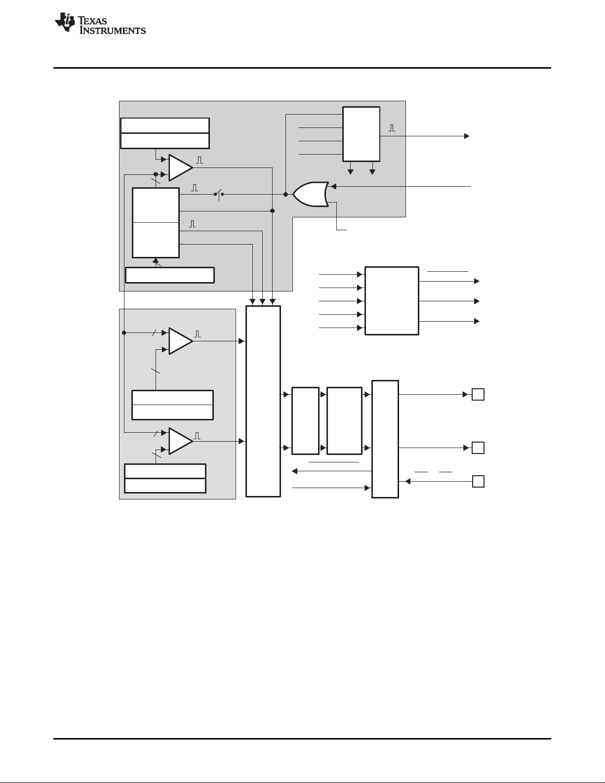
Figure 3 shows more internal details of a single ePWM module. The main signals used by the ePWM
module are:
• PWM output signals (EPWMxA and EPWMxB).
• Trip-zone signals (TZ1 to TZ6).
• Time-base synchronization input (EPWMxSYNCI) and output (EPWMxSYNCO) signals.
• ADC start-of-conversion signals (EPWMxSOCA and EPWMxSOCB).
• Peripheral Bus
www.ti.com
Figure 2. Submodules and Signal Connections for an ePWM Module
The PWM output signals are made available external to the device through the GPIO peripheral
described in the system control and interrupts guide for your device.
These input signals alert the ePWM module of fault conditions external to the ePWM module. Each
module on a device can be configured to either use or ignore any of the trip-zone signals. The TZ1 to
TZ6 trip-zone signals can be configured as asynchronous inputs through the GPIO peripheral.
The synchronization signals daisy chain the ePWM modules together. Each module can be configured
to either use or ignore its synchronization input. The clock synchronization input and output signal are
brought out to pins only for ePWM1 (ePWM module #1). The synchronization output for ePWM1
(EPWM1SYNCO) is also connected to the SYNCI of the first enhanced capture module (eCAP1).
Each ePWM module has two ADC start of conversion signals (one for each sequencer). Any ePWM
module can trigger a start of conversion for either sequencer. Which event triggers the start of
conversion is configured in the Event-Trigger submodule of the ePWM.
The peripheral bus is 32-bits wide and allows both 16-bit and 32-bit writes to the ePWM register file.
14
TMS320x2833x, 2823x Enhanced Pulse Width Modulator (ePWM) Module SPRUG04A–October 2008–Revised July 2009
© 2008–2009, Texas Instruments Incorporated
Submit Documentation Feedback
Page 15
Action
qualifier
(AQ)
Time-base (TB)
Dead
band
(DB)
Counter compare (CC)
Trip
zone
(TZ)
Event
trigger and
interrupt
(ET)
PWM
chopper
(PC)
TZ1 to TZ6
TBPRD shadow (16)
TBPRD active (16)
CTR = PRD
CTR = ZERO
CTR = CMPA
CTR = CMPB
CTR_Dir
TBCTL[SWFSYNC] (software
forced sync)
TBPHS active (16)
Counter
UP/DWN
(16 bit)
TBCTR
active
(16)
Sync
in/out
select
MUX
S0
S1
CMPA active (16)
CMPA shadow (16)
CMPB active (16)
CMPB shadow (16)
EPWMxA
EPWMxB
EPWMxSOCB
EPWMxSOCA
EPWMxINT
EPWMxSYNCI
EPWMxSYNCO
TBCTL[SWFSYNC]
CTR_PRD
TBCTL[PHSEN]
CTR_Dir
CTR = ZERO
CTR = CMPA
CTR = CMPB
16
16
16
16
16
16
Phase
control
EPWMxTZINT
CTR=ZERO
www.ti.com
Introduction
Figure 3. ePWM Submodules and Critical Internal Signal Interconnects
1.2 Register Mapping
SPRUG04A–October 2008–Revised July 2009 TMS320x2833x, 2823x Enhanced Pulse Width Modulator (ePWM) Module
Submit Documentation Feedback
Figure 3 also shows the key internal submodule interconnect signals. Each submodule is described in
detail in its respective section.
The complete ePWM module control and status register set is grouped by submodule as shown in
Table 1. Each register set is duplicated for each instance of the ePWM module. The start address for each
ePWM register file instance on a device is specified in the appropriate data manual.
© 2008–2009, Texas Instruments Incorporated
15
Page 16

Introduction
TBCTL 0x0000 1 No Time-Base Control Register
TBSTS 0x0001 1 No Time-Base Status Register
TBPHSHR 0x0002 1 No Extension for HRPWM Phase Register
TBPHS 0x0003 1 No Time-Base Phase Register
TBCTR 0x0004 1 No Time-Base Counter Register
TBPRD 0x0005 1 Yes Time-Base Period Register
CMPCTL 0x0007 1 No Counter-Compare Control Register
CMPAHR 0x0008 1 Yes Extension for HRPWM Counter-Compare A Register
CMPA 0x0009 1 Yes Counter-Compare A Register
CMPB 0x000A 1 Yes Counter-Compare B Register
AQCTLA 0x000B 1 No Action-Qualifier Control Register for Output A (EPWMxA)
AQCTLB 0x000C 1 No Action-Qualifier Control Register for Output B (EPWMxB)
AQSFRC 0x000D 1 No Action-Qualifier Software Force Register
AQCSFRC 0x000E 1 Yes Action-Qualifier Continuous S/W Force Register Set
DBCTL 0x000F 1 No Dead-Band Generator Control Register
DBRED 0x0010 1 No Dead-Band Generator Rising Edge Delay Count Register
DBFED 0x0011 1 No Dead-Band Generator Falling Edge Delay Count Register
TZSEL 0x0012 1 Yes Trip-Zone Select Register
TZCTL 0x0014 1 Yes Trip-Zone Control Register
TZEINT 0x0015 1 Yes Trip-Zone Enable Interrupt Register
TZFLG 0x0016 1 Trip-Zone Flag Register
TZCLR 0x0017 1 Yes Trip-Zone Clear Register
TZFRC 0x0018 1 Yes Trip-Zone Force Register
ETSEL 0x0019 1 Event-Trigger Selection Register
ETPS 0x001A 1 Event-Trigger Pre-Scale Register
ETFLG 0x001B 1 Event-Trigger Flag Register
ETCLR 0x001C 1 Event-Trigger Clear Register
ETFRC 0x001D 1 Event-Trigger Force Register
PCCTL 0x001E 1 PWM-Chopper Control Register
HRCNFG 0x0020 1 Yes HRPWM Configuration Register
(1)
(2)
(3)
www.ti.com
Table 1. ePWM Module Control and Status Register Set Grouped by Submodule
Offset Size
Name
Locations not shown are reserved.
These registers are only available on ePWM instances that include the high-resolution PWM extension. Otherwise these
locations are reserved. These registers are described in the TMS320x2833x, 2823x High-Resolution Pulse Width Modulator
(HRPWM) Reference Guide (SPRUG02) . See the device specific data manual to determine which instances include the
HRPWM.
EALLOW protected registers as described in the specific device version of the System Control and Interrupts Reference Guide
listed in Related Documentation From Texas Instruments.
(1)
(x16) Shadow EALLOW Description
Time-Base Submodule Registers
(2)
Counter-Compare Submodule Registers
(2)
Action-Qualifier Submodule Registers
Dead-Band Generator Submodule Registers
Trip-Zone Submodule Registers
(3)
(3)
(3)
(3)
(3)
Event-Trigger Submodule Registers
PWM-Chopper Submodule Registers
High-Resolution Pulse Width Modulator (HRPWM) Extension
Registers
(2) (3)
16
TMS320x2833x, 2823x Enhanced Pulse Width Modulator (ePWM) Module SPRUG04A–October 2008–Revised July 2009
Submit Documentation Feedback
© 2008–2009, Texas Instruments Incorporated
Page 17

www.ti.com
2 ePWM Submodules
Seven submodules are included in every ePWM peripheral. Each of these submodules performs specific
tasks that can be configured by software.
2.1 Overview
Table 2 lists the seven key submodules together with a list of their main configuration parameters. For
example, if you need to adjust or control the duty cycle of a PWM waveform, then you should see the
counter-compare submodule in Section 2.3 for relevant details.
Submodule Configuration Parameter or Option
Time-base (TB)
Counter-compare (CC)
Action-qualifier (AQ)
Dead-band (DB)
PWM-chopper (PC)
ePWM Submodules
Table 2. Submodule Configuration Parameters
• Scale the time-base clock (TBCLK) relative to the system clock (SYSCLKOUT).
• Configure the PWM time-base counter (TBCTR) frequency or period.
• Set the mode for the time-base counter:
– count-up mode: used for asymmetric PWM
– count-down mode: used for asymmetric PWM
– count-up-and-down mode: used for symmetric PWM
• Configure the time-base phase relative to another ePWM module.
• Synchronize the time-base counter between modules through hardware or software.
• Configure the direction (up or down) of the time-base counter after a synchronization event.
• Configure how the time-base counter will behave when the device is halted by an emulator.
• Specify the source for the synchronization output of the ePWM module:
– Synchronization input signal
– Time-base counter equal to zero
– Time-base counter equal to counter-compare B (CMPB)
– No output synchronization signal generated.
• Specify the PWM duty cycle for output EPWMxA and/or output EPWMxB
• Specify the time at which switching events occur on the EPWMxA or EPWMxB output
• Specify the type of action taken when a time-base or counter-compare submodule event occurs:
– No action taken
– Output EPWMxA and/or EPWMxB switched high
– Output EPWMxA and/or EPWMxB switched low
– Output EPWMxA and/or EPWMxB toggled
• Force the PWM output state through software control
• Configure and control the PWM dead-band through software
• Control of traditional complementary dead-band relationship between upper and lower switches
• Specify the output rising-edge-delay value
• Specify the output falling-edge delay value
• Bypass the dead-band module entirely. In this case the PWM waveform is passed through
without modification.
• Create a chopping (carrier) frequency.
• Pulse width of the first pulse in the chopped pulse train.
• Duty cycle of the second and subsequent pulses.
• Bypass the PWM-chopper module entirely. In this case the PWM waveform is passed through
without modification.
SPRUG04A–October 2008–Revised July 2009 TMS320x2833x, 2823x Enhanced Pulse Width Modulator (ePWM) Module
Submit Documentation Feedback
© 2008–2009, Texas Instruments Incorporated
17
Page 18

ePWM Submodules
Submodule Configuration Parameter or Option
Trip-zone (TZ)
Event-trigger (ET) • Enable the ePWM events that will trigger an interrupt.
Code examples are provided in the remainder of this document that show how to implement various
ePWM module configurations. These examples use the constant definitions shown in Example 1. These
definitions are also used in the C2833x/2823x C/C++ Header Files and Peripheral Examples (SPRC530) .
www.ti.com
Table 2. Submodule Configuration Parameters (continued)
• Configure the ePWM module to react to one, all, or none of the trip-zone pins .
• Specify the tripping action taken when a fault occurs:
– Force EPWMxA and/or EPWMxB high
– Force EPWMxA and/or EPWMxB low
– Force EPWMxA and/or EPWMxB to a high-impedance state
– Configure EPWMxA and/or EPWMxB to ignore any trip condition.
• Configure how often the ePWM will react to each trip-zone pins :
– One-shot
– Cycle-by-cycle
• Enable the trip-zone to initiate an interrupt.
• Bypass the trip-zone module entirely.
• Enable ePWM events that will trigger an ADC start-of-conversion event.
• Specify the rate at which events cause triggers (every occurrence or every second or third
occurrence)
• Poll, set, or clear event flags
Example 1. Constant Definitions Used in the Code Examples
// TBCTL (Time-Base Control)
// = = = = = = = = = = = = = = = = = = = = = = = = = =
// TBCTR MODE bits
#define TB_COUNT_UP 0x0
#define TB_COUNT_DOWN 0x1
#define TB_COUNT_UPDOWN 0x2
#define TB_FREEZE 0x3
// PHSEN bit
#define TB_DISABLE 0x0
#define TB_ENABLE 0x1
// PRDLD bit
#define TB_SHADOW 0x0
#define TB_IMMEDIATE 0x1
// SYNCOSEL bits
#define TB_SYNC_IN 0x0
#define TB_CTR_ZERO 0x1
#define TB_CTR_CMPB 0x2
#define TB_SYNC_DISABLE 0x3
// HSPCLKDIV and CLKDIV bits
#define TB_DIV1 0x0
#define TB_DIV2 0x1
#define TB_DIV4 0x2
// PHSDIR bit
#define TB_DOWN 0x0
#define TB_UP 0x1
// CMPCTL (Compare Control)
// = = = = = = = = = = = = = = = = = = = = = = = = = =
//
LOADAMODE and LOADBMODE bits
#define CC_CTR_ZERO 0x0
#define CC_CTR_PRD 0x1
#define CC_CTR_ZERO_PRD 0x2 #
define CC_LD_DISABLE 0x3
// SHDWAMODE and SHDWBMODE bits
#define CC_SHADOW 0x0
#define CC_IMMEDIATE 0x1
// AQCTLA and AQCTLB (Action-qualifier Control)
// = = = = = = = = = = = = = = = = = = = = = = = = = =
// ZRO, PRD, CAU, CAD, CBU, CBD bits
18
TMS320x2833x, 2823x Enhanced Pulse Width Modulator (ePWM) Module SPRUG04A–October 2008–Revised July 2009
Submit Documentation Feedback
© 2008–2009, Texas Instruments Incorporated
Page 19

www.ti.com
Example 1. Constant Definitions Used in the Code Examples (continued)
#define AQ_NO_ACTION 0x0
#define AQ_CLEAR 0x1
#define AQ_SET 0x2
#define AQ_TOGGLE 0x3
// DBCTL (Dead-Band Control)
// = = = = = = = = = = = = = = = = = = = = = = = = = =
// MODE bits
#define DB_DISABLE 0x0
#define DBA_ENABLE 0x1
#define DBB_ENABLE 0x2
#define DB_FULL_ENABLE 0x3
// POLSEL bits
#define DB_ACTV_HI 0x0
#define DB_ACTV_LOC 0x1
#define DB_ACTV_HIC 0x2
#define DB_ACTV_LO 0x3 // PCCTL (chopper control)
// = = = = = = = = = = = = = = = = = = = = = = = = = =
// CHPEN bit
#define CHP_ENABLE 0x0
#define CHP_DISABLE 0x1
// CHPFREQ bits
#define CHP_DIV1 0x0
#define CHP_DIV2 0x1
#define CHP_DIV3 0x2
#define CHP_DIV4 0x3
#define CHP_DIV5 0x4
#define CHP_DIV6 0x5
#define CHP_DIV7 0x6
#define CHP_DIV8 0x7
// CHPDUTY bits
#define CHP1_8TH 0x0
#define CHP2_8TH 0x1
#define CHP3_8TH 0x2
#define CHP4_8TH 0x3
#define CHP5_8TH 0x4
#define CHP6_8TH 0x5 #
define CHP7_8TH 0x6
// TZSEL (Trip-zone Select)
// = = = = = = = = = = = = = = = = = = = = = = = = = =
// CBCn and OSHTn bits
#define TZ_ENABLE 0x0
#define TZ_DISABLE 0x1
// TZCTL (Trip-zone Control)
// = = = = = = = = = = = = = = = = = = = = = = = = = =
// TZA and TZB bits
#define TZ_HIZ 0x0
#define TZ_FORCE_HI 0x1
#define TZ_FORCE_LO 0x2
#define TZ_DISABLE 0x3
// ETSEL (Event-trigger Select)
// = = = = = = = = = = = = = = = = = = = = = = = = = =
// INTSEL, SOCASEL, SOCBSEL bits
#define ET_CTR_ZERO 0x1
#define ET_CTR_PRD 0x2
#define ET_CTRU_CMPA 0x4
#define ET_CTRD_CMPA 0x5
#define ET_CTRU_CMPB 0x6
#define ET_CTRD_CMPB 0x7
// ETPS (Event-trigger Prescale)
// = = = = = = = = = = = = = = = = = = = = = = = = = =
// INTPRD, SOCAPRD, SOCBPRD bits
#define ET_DISABLE 0x0
#define ET_1ST 0x1
#define ET_2ND 0x2
#define ET_3RD 0x3
ePWM Submodules
SPRUG04A–October 2008–Revised July 2009 TMS320x2833x, 2823x Enhanced Pulse Width Modulator (ePWM) Module
Submit Documentation Feedback
© 2008–2009, Texas Instruments Incorporated
19
Page 20

CTR = CMPB
CTR = CMPA
CTR_Dir
CTR = 0
CTR = PRD
Dead
Band
(DB)
Counter
Compare
(CC)
Action
Qualifier
(AQ)
EPWMxA
EPWMxB
CTR = CMPB
CTR = 0
EPWMxINT
EPWMxSOCA
EPWMxSOCB
EPWMxA
EPWMxB
TZ1 to TZ6
CTR = CMPA
Time-Base
(TB)
CTR = PRD
CTR = 0
CTR_Dir
EPWMxSYNCI
EPWMxSYNCO
EPWMxTZINT
PWM-
chopper
(PC)
Event
Trigger
and
Interrupt
(ET)
Trip
Zone
(TZ)
GPIO
MUX
ADC
PIE
PIE
ePWM Submodules
2.2 Time-Base (TB) Submodule
Each ePWM module has its own time-base submodule that determines all of the event timing for the
ePWM module. Built-in synchronization logic allows the time-base of multiple ePWM modules to work
together as a single system. Figure 4 illustrates the time-base module's place within the ePWM.
Figure 4. Time-Base Submodule Block Diagram
www.ti.com
2.2.1 Purpose of the Time-Base Submodule
You can configure the time-base submodule for the following:
• Specify the ePWM time-base counter (TBCTR) frequency or period to control how often events occur.
• Manage time-base synchronization with other ePWM modules.
• Maintain a phase relationship with other ePWM modules.
• Set the time-base counter to count-up, count-down, or count-up-and-down mode.
• Generate the following events:
– CTR = PRD: Time-base counter equal to the specified period (TBCTR = TBPRD) .
– CTR = Zero: Time-base counter equal to zero (TBCTR = 0x0000).
• Configure the rate of the time-base clock; a prescaled version of the CPU system clock
(SYSCLKOUT). This allows the time-base counter to increment/decrement at a slower rate.
20
TMS320x2833x, 2823x Enhanced Pulse Width Modulator (ePWM) Module SPRUG04A–October 2008–Revised July 2009
© 2008–2009, Texas Instruments Incorporated
Submit Documentation Feedback
Page 21

TBCTL[SYNCOSEL]
TBPRD
PeriodActive
TBPRD
PeriodShadow
16
TBCTL[SWFSYNC]
CTR=PRD
TBPHS
PhaseActiveReg
Counter
UP/DOWN
16
Sync
Out
Select
EPWMxSYNCO
Reset
Load
16
TBCTL[PHSEN]
CTR=Zero
CTR=CMPB
Disable
X
EPWMxSYNCI
TBCTL[PRDLD]
TBCTR[15:0]
Mode
TBCTL[CTRMODE]
CTR=Zero
CTR_max
TBCLK
Clock
Prescale
SYSCLKOUT
TBCLK
TBCTL[HSPCLKDIV]
TBCTL[CLKDIV]
CTR_dir
TBCTR
CounterActiveReg
clk
Max
Dir
Zero
www.ti.com
2.2.2 Controlling and Monitoring the Time-base Submodule
Table 3 shows the registers used to control and monitor the time-base submodule.
Table 3. Time-Base Submodule Registers
Register Address offset Shadowed Description
TBCTL 0x0000 No Time-Base Control Register
TBSTS 0x0001 No Time-Base Status Register
TBPHSHR 0x0002 No HRPWM Extension Phase Register
TBPHS 0x0003 No Time-Base Phase Register
TBCTR 0x0004 No Time-Base Counter Register
TBPRD 0x0005 Yes Time-Base Period Register
(1)
This register is available only on ePWM instances that include the high-resolution extension (HRPWM). On ePWM modules that
do not include the HRPWM, this location is reserved. This register is described in the device-specific High-Resolution Pulse
Width Modulator (HRPWM) Reference Guide. See the device specific data manual to determine which ePWM instances include
this feature.
The block diagram in Figure 5 shows the critical signals and registers of the time-base submodule.
Table 4 provides descriptions of the key signals associated with the time-base submodule.
Figure 5. Time-Base Submodule Signals and Registers
ePWM Submodules
(1)
SPRUG04A–October 2008–Revised July 2009 TMS320x2833x, 2823x Enhanced Pulse Width Modulator (ePWM) Module
Submit Documentation Feedback
© 2008–2009, Texas Instruments Incorporated
21
Page 22

ePWM Submodules
Signal Description
EPWMxSYNCI Time-base synchronization input.
EPWMxSYNCO Time-base synchronization output.
CTR = PRD Time-base counter equal to the specified period.
CTR = Zero Time-base counter equal to zero
CTR = CMPB Time-base counter equal to active counter-compare B register (TBCTR = CMPB).
CTR_dir Time-base counter direction.
CTR_max Time-base counter equal max value. (TBCTR = 0xFFFF)
TBCLK Time-base clock.
www.ti.com
Table 4. Key Time-Base Signals
Input pulse used to synchronize the time-base counter with the counter of ePWM module earlier in the
synchronization chain. An ePWM peripheral can be configured to use or ignore this signal. For the first ePWM
module (EPWM1) this signal comes from a device pin. For subsequent ePWM modules this signal is passed
from another ePWM peripheral. For example, EPWM2SYNCI is generated by the ePWM1 peripheral,
EPWM3SYNCI is generated by ePWM2 and so forth. See Section 2.2.3.3 for information on the
synchronization order of a particular device.
This output pulse is used to synchronize the counter of an ePWM module later in the synchronization chain.
The ePWM module generates this signal from one of three event sources:
1. EPWMxSYNCI (Synchronization input pulse)
2. CTR = Zero: The time-base counter equal to zero (TBCTR = 0x0000).
3. CTR = CMPB: The time-base counter equal to the counter-compare B (TBCTR = CMPB) register.
This signal is generated whenever the counter value is equal to the active period register value. That is when
TBCTR = TBPRD.
This signal is generated whenever the counter value is zero. That is when TBCTR equals 0x0000.
This event is generated by the counter-compare submodule and used by the synchronization out logic
Indicates the current direction of the ePWM's time-base counter. This signal is high when the counter is
increasing and low when it is decreasing.
Generated event when the TBCTR value reaches its maximum value. This signal is only used only as a status
bit
This is a prescaled version of the system clock (SYSCLKOUT) and is used by all submodules within the
ePWM. This clock determines the rate at which time-base counter increments or decrements.
2.2.3 Calculating PWM Period and Frequency
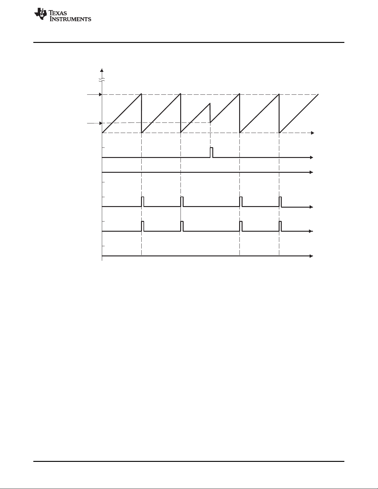
The frequency of PWM events is controlled by the time-base period (TBPRD) register and the mode of the
time-base counter. Figure 6 shows the period (T
down-count, and up-down-count time-base counter modes when when the period is set to 4 (TBPRD = 4).
The time increment for each step is defined by the time-base clock (TBCLK) which is a prescaled version
of the system clock (SYSCLKOUT).
The time-base counter has three modes of operation selected by the time-base control register (TBCTL):
• Up-Down-Count Mode:
In up-down-count mode, the time-base counter starts from zero and increments until the period
(TBPRD) value is reached. When the period value is reached, the time-base counter then decrements
until it reaches zero. At this point the counter repeats the pattern and begins to increment.
• Up-Count Mode:
In this mode, the time-base counter starts from zero and increments until it reaches the value in the
period register (TBPRD). When the period value is reached, the time-base counter resets to zero and
begins to increment once again.
• Down-Count Mode:
In down-count mode, the time-base counter starts from the period (TBPRD) value and decrements until
it reaches zero. When it reaches zero, the time-base counter is reset to the period value and it begins
to decrement once again.
) and frequency (F
pwm
) relationships for the up-count,
pwm
22
TMS320x2833x, 2823x Enhanced Pulse Width Modulator (ePWM) Module SPRUG04A–October 2008–Revised July 2009
Submit Documentation Feedback
© 2008–2009, Texas Instruments Incorporated
Page 23

PRD
4
4 4
PRD
4
1
2
3
0
1
2
3
0
1
2
3
0
Z
1
2
3
4
0
1
2
3
CTR_dir
1
2
3
4
0
1
2
3
0
Up Down Down
Up
T
PWM =
(TBPRD + 1) x T
TBCLK
For Up Count and Down Count
For Up and Down Count
F
PWM =
1/ (T
PWM)
T
PWM =
2 x TBPRD x T
TBCLK
F
PWM =
1 / (T
PWM)
1
2
3
4
0
1
2
3
4
0
1
2
3
0
T
PWM
Z
T
PWM
T
PWM
T
PWM
www.ti.com
ePWM Submodules
Figure 6. Time-Base Frequency and Period
2.2.3.1 Time-Base Period Shadow Register
The time-base period register (TBPRD) has a shadow register. Shadowing allows the register update to
be synchronized with the hardware. The following definitions are used to describe all shadow registers in
the ePWM module:
• Active Register
The active register controls the hardware and is responsible for actions that the hardware causes or
invokes.
• Shadow Register
direct effect on any control hardware. At a strategic point in time the shadow register's content is
transferred to the active register. This prevents corruption or spurious operation due to the register
being asynchronously modified by software.
The memory address of the shadow period register is the same as the active register. Which register is
written to or read from is determined by the TBCTL[PRDLD] bit. This bit enables and disables the TBPRD
shadow register as follows:
• Time-Base Period Shadow Mode:
The shadow register buffers or provides a temporary holding location for the active register. It has no
The TBPRD shadow register is enabled when TBCTL[PRDLD] = 0. Reads from and writes to the
TBPRD memory address go to the shadow register. The shadow register contents are transferred to
the active register (TBPRD (Active) ← TBPRD (shadow)) when the time-base counter equals zero
(TBCTR = 0x0000). By default the TBPRD shadow register is enabled.
• Time-Base Period Immediate Load Mode:
SPRUG04A–October 2008–Revised July 2009 TMS320x2833x, 2823x Enhanced Pulse Width Modulator (ePWM) Module
Submit Documentation Feedback
If immediate load mode is selected (TBCTL[PRDLD] = 1), then a read from or a write to the TBPRD
© 2008–2009, Texas Instruments Incorporated
23
Page 24

ePWM Submodules
memory address goes directly to the active register.
2.2.3.2 Time-Base Clock Synchronization
The TBCLKSYNC bit in the peripheral clock enable registers allows all users to globally synchronize all
enabled ePWM modules to the time-base clock (TBCLK). When set, all enabled ePWM module clocks are
started with the first rising edge of TBCLK aligned. For perfectly synchronized TBCLKs, the prescalers for
each ePWM module must be set identically.
The proper procedure for enabling ePWM clocks is as follows:
1. Enable ePWM module clocks in the PCLKCRx register
2. Set TBCLKSYNC= 0
3. Configure ePWM modules
4. Set TBCLKSYNC=1
2.2.3.3 Time-Base Counter Synchronization
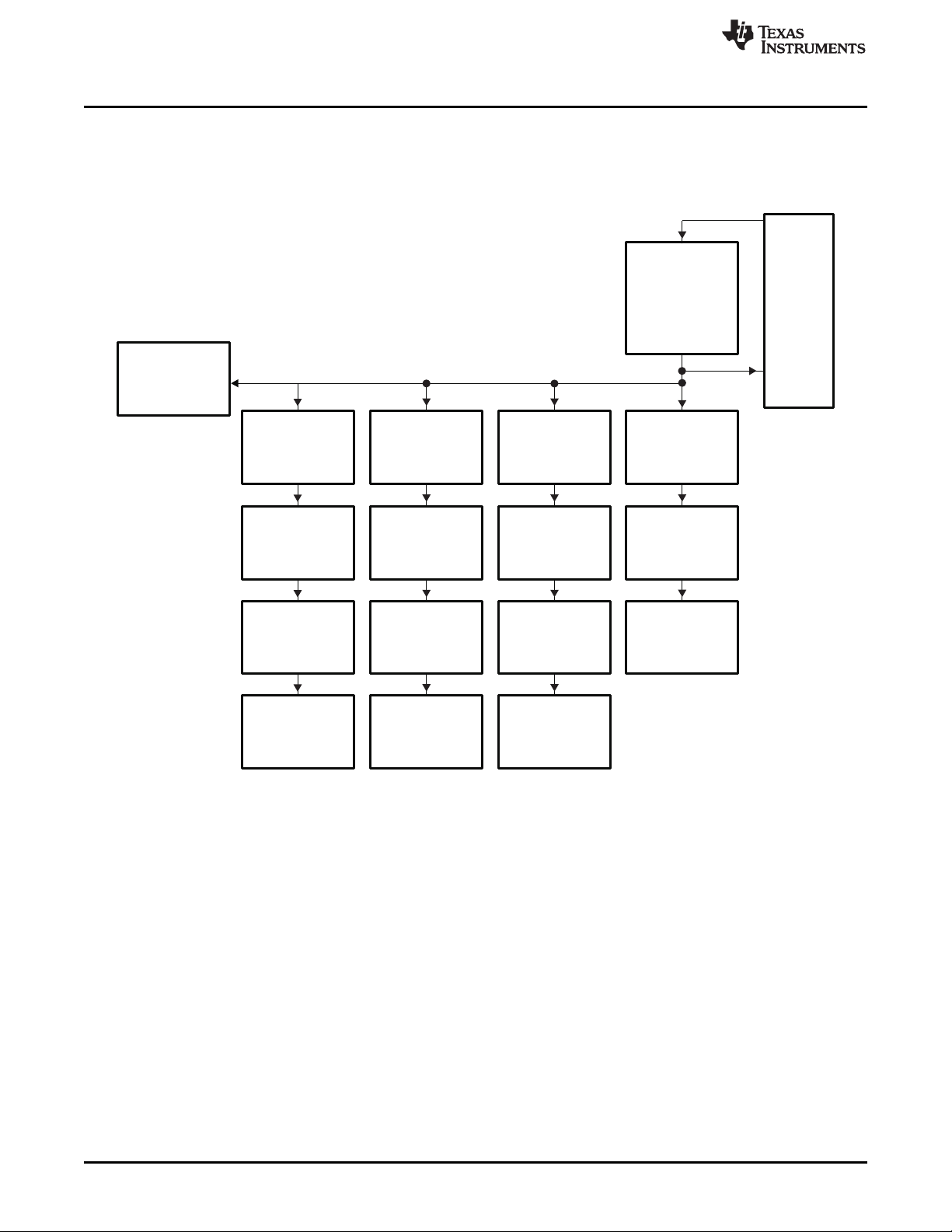
A time-base synchronization scheme connects all of the ePWM modules on a device. Each ePWM
module has a synchronization input (EPWMxSYNCI) and a synchronization output (EPWMxSYNCO). The
input synchronization for the first instance (ePWM1) comes from an external pin. The possible
synchronization connections for the remaining ePWM modules are shown in Figure 7, Figure 8, and
Figure 9.
Scheme 1 shown in Figure 7 applies to the 280x, 2801x, 2802x, and 2803x devices. Scheme 1 also
applies to the 2804x devices when the ePWM pinout is configured for 280x compatible mode
(GPAMCFG[EPWMMODE] = 0).
www.ti.com
24
TMS320x2833x, 2823x Enhanced Pulse Width Modulator (ePWM) Module SPRUG04A–October 2008–Revised July 2009
Submit Documentation Feedback
© 2008–2009, Texas Instruments Incorporated
Page 25

EPWM2SYNCI
ePWM2
EPWM2SYNCO
EPWM1SYNCO
ePWM1
EPWM1SYNCI
GPIO
MUX
EPWM3SYNCO
ePWM3
EPWM3SYNCI
ePWMx
EPWMxSYNCI
SYNCI
eCAP1
EPWMxSYNCO
www.ti.com
ePWM Submodules
Figure 7. Time-Base Counter Synchronization Scheme 1
SPRUG04A–October 2008–Revised July 2009 TMS320x2833x, 2823x Enhanced Pulse Width Modulator (ePWM) Module
Submit Documentation Feedback
© 2008–2009, Texas Instruments Incorporated
25
Page 26
EPWM1SYNCI
ePWM1
EPWM1SYNCO
GPIO
MUX
EPWM2SYNCI
ePWM2
EPWM2SYNCO
EPWM3SYNCI
ePWM3
EPWM3SYNCO
EPWM4SYNCI
ePWM4
EPWM4SYNCO
EPWM5SYNCI
ePWM5
EPWM5SYNCO
EPWM6SYNCI
ePWM6
EPWM36YNCO
EPWM7SYNCI
ePWM7
EPWM7SYNCO
EPWM9SYNCI
ePWM9
EPWM9SYNCO
EPWM10SYNCI
ePWM10
EPWM10SYNCO
EPWM11SYNCI
ePWM11
EPWM11SYNCO
EPWM13SYNCI
ePWM13
EPWM13SYnCO
EPWM14SYNCI
ePWM14
EPWM14SYNCO
EPWM15SYNCI
ePWM15
EPWM15SYNCO
EPWM8SYNCI
ePWM8
EPWM8SYNCO
EPWM12SYNCI
ePWM12
EPWM12SYNCO
EPWM16SYNCI
ePWM16
EPWM16SYNCO
SYNCI
eCAP1
ePWM Submodules
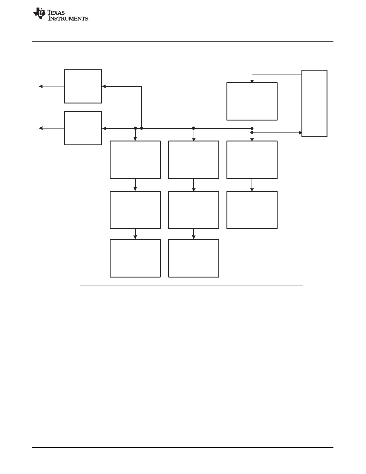
Scheme 2 shown in Figure 8 is used by the 2804x devices when the ePWM pinout is configured for
A-channel only mode (GPAMCFG[EPWMMODE] = 3). If the 2804x ePWM pinout is configured for 280x
compatible mode (GPAMCFG[EPWMMODE] = 0), then Scheme 1 is used.
www.ti.com
Figure 8. Time-Base Counter Synchronization Scheme 2
26
TMS320x2833x, 2823x Enhanced Pulse Width Modulator (ePWM) Module SPRUG04A–October 2008–Revised July 2009
© 2008–2009, Texas Instruments Incorporated
Submit Documentation Feedback
Page 27
EPWM1SYNCO
ePWM1
EPWM1SYNCI
GPIO
MUX
SYNCI
eCAP1
EPWM2SYNCI
ePWM2
EPWM2SYNCO
EPWM3SYNCO
ePWM3
EPWM3SYNCI
EPWM4SYNCI
ePWM4
EPWM4SYNCO
EPWM5SYNCO
ePWM5
EPWM5SYNCI
ePWM6
EPWM6SYNCI
eCAP4
EPWM7SYNCI
ePWM7
EPWM7SYNCO
EPWM8SYNCI
ePWM8
EPWM8SYNCO
EPWM9SYNCI
ePWM9
www.ti.com
Scheme 3, shown in Figure 9, is used by all other devices.
ePWM Submodules
Figure 9. Time-Base Counter Synchronization Scheme 3
NOTE: All modules shown in the synchronization schemes may not be available on all devices.
Please refer to the device specific data manual to determine which modules are available on
a particular device.
Each ePWM module can be configured to use or ignore the synchronization input. If the TBCTL[PHSEN]
bit is set, then the time-base counter (TBCTR) of the ePWM module will be automatically loaded with the
phase register (TBPHS) contents when one of the following conditions occur:
• EPWMxSYNCI: Synchronization Input Pulse:
The value of the phase register is loaded into the counter register when an input synchronization pulse
is detected (TBPHS → TBCTR). This operation occurs on the next valid time-base clock (TBCLK)
edge.
The delay from internal master module to slave modules is given by:
– if ( TBCLK = SYSCLKOUT): 2 x SYSCLKOUT
– if ( TBCLK != SYSCLKOUT):1 TBCLK
• Software Forced Synchronization Pulse:
Writing a 1 to the TBCTL[SWFSYNC] control bit invokes a software forced synchronization. This pulse
is ORed with the synchronization input signal, and therefore has the same effect as a pulse on
EPWMxSYNCI.
• This feature enables the ePWM module to be automatically synchronized to the time base of another
SPRUG04A–October 2008–Revised July 2009 TMS320x2833x, 2823x Enhanced Pulse Width Modulator (ePWM) Module
Submit Documentation Feedback
© 2008–2009, Texas Instruments Incorporated
27
Page 28

ePWM Submodules
ePWM module. Lead or lag phase control can be added to the waveforms generated by different
ePWM modules to synchronize them. In up-down-count mode, the TBCTL[PSHDIR] bit configures the
direction of the time-base counter immediately after a synchronization event. The new direction is
independent of the direction prior to the synchronization event. The PHSDIR bit is ignored in count-up
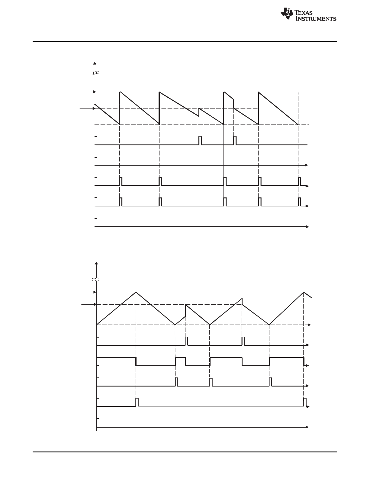
or count-down modes. See Figure 10 through Figure 13 for examples.
Clearing the TBCTL[PHSEN] bit configures the ePWM to ignore the synchronization input pulse. The
synchronization pulse can still be allowed to flow-through to the EPWMxSYNCO and be used to
synchronize other ePWM modules. In this way, you can set up a master time-base (for example, ePWM1)
and downstream modules (ePWM2 - ePWMx) may elect to run in synchronization with the master. See
the Application to Power Topologies Section 3 for more details on synchronization strategies.
2.2.4 Phase Locking the Time-Base Clocks of Multiple ePWM Modules
The TBCLKSYNC bit can be used to globally synchronize the time-base clocks of all enabled ePWM
modules on a device. This bit is part of the device's clock enable registers and is described in the specific
device version of the System Control and Interrupts Reference Guide listed in Related Documentation
From Texas Instruments. When TBCLKSYNC = 0, the time-base clock of all ePWM modules is stopped
(default). When TBCLKSYNC = 1, all ePWM time-base clocks are started with the rising edge of TBCLK
aligned. For perfectly synchronized TBCLKs, the prescaler bits in the TBCTL register of each ePWM
module must be set identically. The proper procedure for enabling the ePWM clocks is as follows:
1. Enable the individual ePWM module clocks. This is described in the specific device version of the
System Control and Interrupts Reference Guide listed in Related Documentation From Texas
Instruments.
2. Set TBCLKSYNC = 0. This will stop the time-base clock within any enabled ePWM module.
3. Configure the prescaler values and desired ePWM modes.
4. Set TBCLKSYNC = 1.
www.ti.com
2.2.5 Time-base Counter Modes and Timing Waveforms
The time-base counter operates in one of four modes:
• Up-count mode which is asymmetrical.
• Down-count mode which is asymmetrical.
• Up-down-count which is symmetrical
• Frozen where the time-base counter is held constant at the current value
To illustrate the operation of the first three modes, the following timing diagrams show when events are
generated and how the time-base responds to an EPWMxSYNCI signal.
28
TMS320x2833x, 2823x Enhanced Pulse Width Modulator (ePWM) Module SPRUG04A–October 2008–Revised July 2009
Submit Documentation Feedback
© 2008–2009, Texas Instruments Incorporated
Page 29
0000
TBCTR[15:0]
CTR_dir
CTR = zero
CNT_max
CTR = PRD
0xFFFF
TBPHS
(value)
TBPRD
(value)
www.ti.com
ePWM Submodules
Figure 10. Time-Base Up-Count Mode Waveforms
SPRUG04A–October 2008–Revised July 2009 TMS320x2833x, 2823x Enhanced Pulse Width Modulator (ePWM) Module
Submit Documentation Feedback
© 2008–2009, Texas Instruments Incorporated
29
Page 30
0x000
0xFFFF
TBCTR[15:0]
TBPHS
(value)
TBPRD
(value)
CTR_dir
CTR = zero
CNT_max
CTR = PRD
0x0000
0xFFFF
TBCTR[15:0]
UP
DOWN
UP
DOWN
UP
DOWN
UP
TBPHS
(value)
TBPRD
(value)
CTR_dir
CTR=zero
CNT_max
CTR=PRD
ePWM Submodules
www.ti.com
Figure 11. Time-Base Down-Count Mode Waveforms
Figure 12. Time-Base Up-Down-Count Waveforms, TBCTL[PHSDIR = 0] Count Down On Synchronization
Event
30
TMS320x2833x, 2823x Enhanced Pulse Width Modulator (ePWM) Module SPRUG04A–October 2008–Revised July 2009
Submit Documentation Feedback
© 2008–2009, Texas Instruments Incorporated
Page 31

0x0000
0xFFFF
TBCTR[15:0]
UP
DOWN
UP
DOWN
UP
DOWN
TBPHS(value)
TBPRD(value)
EPWMxSYNCI
CTR_dir
CTR=zero
CNT_max
CTR=PRD
CTR = CMPB
CTR = CMPA
CTR_Dir
CTR = 0
CTR = PRD
Dead
Band
(DB)
Counter
Compare
(CC)
Action
Qualifier
(AQ)
EPWMxA
EPWMxB
CTR = CMPB
CTR = 0
EPWMxINT
EPWMxSOCA
EPWMxSOCB
EPWMxA
EPWMxB
TZ1 to TZ6
CTR = CMPA
Time-Base
(TB)
CTR = PRD
CTR = 0
CTR_Dir
EPWMxSYNCI
EPWMxSYNCO
EPWMxTZINT
PWM-
chopper
(PC)
Event
Trigger
and
Interrupt
(ET)
Trip
Zone
(TZ)
GPIO
MUX
ADC
PIE
PIE
www.ti.com
ePWM Submodules
Figure 13. Time-Base Up-Down Count Waveforms, TBCTL[PHSDIR = 1] Count Up On Synchronization
Event
2.3 Counter-Compare (CC) Submodule
Figure 14 illustrates the counter-compare submodule within the ePWM.
Figure 14. Counter-Compare Submodule
Figure 15 shows the basic structure of the counter-compare submodule.
SPRUG04A–October 2008–Revised July 2009 TMS320x2833x, 2823x Enhanced Pulse Width Modulator (ePWM) Module
Submit Documentation Feedback
© 2008–2009, Texas Instruments Incorporated
31
Page 32
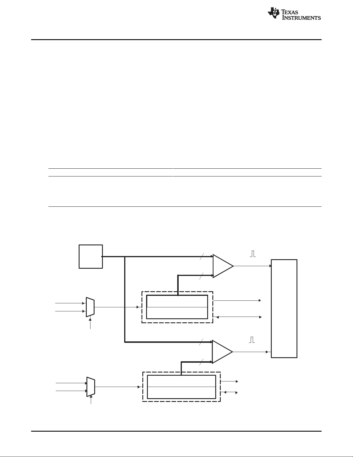
TBCTR[15:0]
Time
Base
(TB)
Module
16
CMPA[15:0]
16
16
16
CMPA
CompareAActiveReg.
CTR=CMPA
CTR=CMPB
Action
Qualifier
Module
Digital
comparatorB
CMPB[15:0]
TBCTR[15:0]
CTR=PRD
CTR=0
CMPCTL[LOADAMODE]
Shadow
load
CTR=PRD
CTR=0
CMPCTL[LOADBMODE]
CMPCTL[SHDWBFULL]
CMPCTL[SHDWBMODE]
CMPCTL
[SHDWAFULL]
CMPCTL
[SHDWAMODE]
CMPA
CompareAShadowReg.
Digital
comparatorA
CMPB
CompareBActiveReg.
CMPB
CompareBShadowReg.
Shadow
load
(AQ)
ePWM Submodules
2.3.1 Purpose of the Counter-Compare Submodule
The counter-compare submodule takes as input the time-base counter value. This value is continuously
compared to the counter-compare A (CMPA) and counter-compare B (CMPB) registers. When the
time-base counter is equal to one of the compare registers, the counter-compare unit generates an
appropriate event.
The counter-compare:
• Generates events based on programmable time stamps using the CMPA and CMPB registers
– CTR = CMPA: Time-base counter equals counter-compare A register (TBCTR = CMPA).
– CTR = CMPB: Time-base counter equals counter-compare B register (TBCTR = CMPB)
• Controls the PWM duty cycle if the action-qualifier submodule is configured appropriately
• Shadows new compare values to prevent corruption or glitches during the active PWM cycle
2.3.2 Controlling and Monitoring the Counter-Compare Submodule
The counter-compare submodule operation is controlled and monitored by the registers shown in Table 5:
Table 5. Counter-Compare Submodule Registers
Register Name Address Offset Shadowed Description
CMPCTL 0x0007 No Counter-Compare Control Register.
CMPAHR 0x0008 Yes HRPWM Counter-Compare A Extension Register
CMPA 0x0009 Yes Counter-Compare A Register
CMPB 0x000A Yes Counter-Compare B Register
(1)
This register is available only on ePWM modules with the high-resolution extension (HRPWM). On ePWM modules that do not
include the HRPWM this location is reserved. This register is described in the device-specific High-Resolution Pulse Width
Modulator (HRPWM) Reference Guide. Refer to the device specific data manual to determine which ePWM instances include
this feature.
www.ti.com
(1)
Figure 15. Detailed View of the Counter-Compare Submodule
32
The key signals associated with the counter-compare submodule are described in Table 6.
TMS320x2833x, 2823x Enhanced Pulse Width Modulator (ePWM) Module SPRUG04A–October 2008–Revised July 2009
© 2008–2009, Texas Instruments Incorporated
Submit Documentation Feedback
Page 33

www.ti.com
Table 6. Counter-Compare Submodule Key Signals
Signal Description of Event Registers Compared
CTR = CMPA Time-base counter equal to the active counter-compare A value TBCTR = CMPA
CTR = CMPB Time-base counter equal to the active counter-compare B value TBCTR = CMPB
CTR = PRD Time-base counter equal to the active period. TBCTR = TBPRD
Used to load active counter-compare A and B registers from the
shadow register
CTR = ZERO Time-base counter equal to zero. TBCTR = 0x0000
Used to load active counter-compare A and B registers from the
shadow register
2.3.3 Operational Highlights for the Counter-Compare Submodule
The counter-compare submodule is responsible for generating two independent compare events based on
two compare registers:
1. CTR = CMPA: Time-base counter equal to counter-compare A register (TBCTR = CMPA).
2. CTR = CMPB: Time-base counter equal to counter-compare B register (TBCTR = CMPB).
For up-count or down-count mode, each event occurs only once per cycle. For up-down-count mode each
event occurs twice per cycle if the compare value is between 0x0000-TBPRD and once per cycle if the
compare value is equal to 0x0000 or equal to TBPRD. These events are fed into the action-qualifier
submodule where they are qualified by the counter direction and converted into actions if enabled. Refer
to Section 2.4.1 for more details.
ePWM Submodules
The counter-compare registers CMPA and CMPB each have an associated shadow register. Shadowing
provides a way to keep updates to the registers synchronized with the hardware. When shadowing is
used, updates to the active registers only occur at strategic points. This prevents corruption or spurious
operation due to the register being asynchronously modified by software. The memory address of the
active register and the shadow register is identical. Which register is written to or read from is determined
by the CMPCTL[SHDWAMODE] and CMPCTL[SHDWBMODE] bits. These bits enable and disable the
CMPA shadow register and CMPB shadow register respectively. The behavior of the two load modes is
described below:
Shadow Mode:
The shadow mode for the CMPA is enabled by clearing the CMPCTL[SHDWAMODE] bit and the shadow
register for CMPB is enabled by clearing the CMPCTL[SHDWBMODE] bit. Shadow mode is enabled by
default for both CMPA and CMPB.
If the shadow register is enabled then the content of the shadow register is transferred to the active
register on one of the following events as specified by the CMPCTL[LOADAMODE] and
CMPCTL[LOADBMODE] register bits:
• CTR = PRD: Time-base counter equal to the period (TBCTR = TBPRD).
• CTR = Zero: Time-base counter equal to zero (TBCTR = 0x0000)
• Both CTR = PRD and CTR = Zero
Only the active register contents are used by the counter-compare submodule to generate events to be
sent to the action-qualifier.
Immediate Load Mode:
If immediate load mode is selected (i.e., TBCTL[SHADWAMODE] = 1 or TBCTL[SHADWBMODE] = 1),
then a read from or a write to the register will go directly to the active register.
2.3.4 Count Mode Timing Waveforms
The counter-compare module can generate compare events in all three count modes:
• Up-count mode: used to generate an asymmetrical PWM waveform.
• Down-count mode: used to generate an asymmetrical PWM waveform.
• Up-down-count mode: used to generate a symmetrical PWM waveform.
SPRUG04A–October 2008–Revised July 2009 TMS320x2833x, 2823x Enhanced Pulse Width Modulator (ePWM) Module
Submit Documentation Feedback
© 2008–2009, Texas Instruments Incorporated
33
Page 34

ePWM Submodules
To best illustrate the operation of the first three modes, the timing diagrams in Figure 16 through Figure 19
show when events are generated and how the EPWMxSYNCI signal interacts.
www.ti.com
34
TMS320x2833x, 2823x Enhanced Pulse Width Modulator (ePWM) Module SPRUG04A–October 2008–Revised July 2009
Submit Documentation Feedback
© 2008–2009, Texas Instruments Incorporated
Page 35
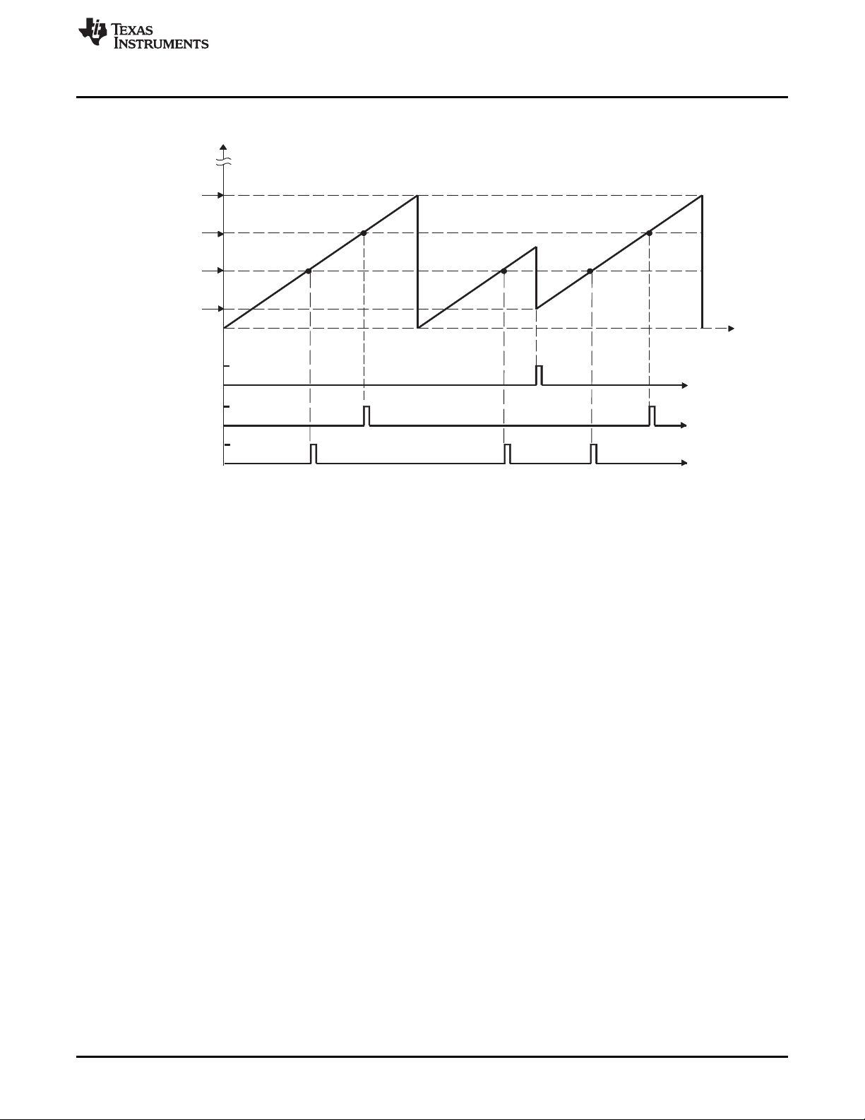
0x0000
0xFFFF
CTR=CMPA
TBCTR[15:0]
CMPA
(value)
CMPB
(value)
TBPHS
(value)
TBPRD
(value)
CTR=CMPB
EPWMxSYNCI
www.ti.com
ePWM Submodules
Figure 16. Counter-Compare Event Waveforms in Up-Count Mode
NOTE: An EPWMxSYNCI external synchronization event can cause a discontinuity in the TBCTR count
sequence. This can lead to a compare event being skipped. This skipping is considered normal operation
and must be taken into account.
SPRUG04A–October 2008–Revised July 2009 TMS320x2833x, 2823x Enhanced Pulse Width Modulator (ePWM) Module
Submit Documentation Feedback
© 2008–2009, Texas Instruments Incorporated
35
Page 36

TBCTR[15:0]
0x0000
0xFFFF
CTR=CMPA
CMPA
(value)
CMPB
(value)
TBPHS
(value)
TBPRD
(value)
CTR=CMPB
EPWMxSYNCI
ePWM Submodules
www.ti.com
Figure 17. Counter-Compare Events in Down-Count Mode
36
TMS320x2833x, 2823x Enhanced Pulse Width Modulator (ePWM) Module SPRUG04A–October 2008–Revised July 2009
Submit Documentation Feedback
© 2008–2009, Texas Instruments Incorporated
Page 37

0x0000
0xFFFF
TBCTR[15:0]
CTR = CMPA
CMPA (value)
CMPB (value)
TBPHS (value)
TBPRD (value)
CTR = CMPB
EPWMxSYNCI
0x0000
0xFFFF
TBCTR[15:0]
CMPA
(value)
CMPB
(value)
TBPHS
(value)
TBPRD
(value)
CTR = CMPA
CTR = CMPB
EPWMxSYNCI
www.ti.com
ePWM Submodules
Figure 18. Counter-Compare Events In Up-Down-Count Mode, TBCTL[PHSDIR = 0] Count Down On
Synchronization Event
Figure 19. Counter-Compare Events In Up-Down-Count Mode, TBCTL[PHSDIR = 1] Count Up On
Synchronization Event
2.4 Action-Qualifier (AQ) Submodule
Figure 20 shows the action-qualifier (AQ) submodule (see shaded block) in the ePWM system.
SPRUG04A–October 2008–Revised July 2009 TMS320x2833x, 2823x Enhanced Pulse Width Modulator (ePWM) Module
Submit Documentation Feedback
© 2008–2009, Texas Instruments Incorporated
37
Page 38

CTR = CMPB
CTR = CMPA
CTR_Dir
CTR = 0
CTR = PRD
Dead
Band
(DB)
Counter
Compare
(CC)
Action
Qualifier
(AQ)
EPWMxA
EPWMxB
CTR = CMPB
CTR = 0
EPWMxINT
EPWMxSOCA
EPWMxSOCB
EPWMxA
EPWMxB
TZ1 to TZ6
CTR = CMPA
Time-Base
(TB)
CTR = PRD
CTR = 0
CTR_Dir
EPWMxSYNCI
EPWMxSYNCO
EPWMxTZINT
PWM-
chopper
(PC)
Event
Trigger
and
Interrupt
(ET)
Trip
Zone
(TZ)
GPIO
MUX
ADC
PIE
PIE
ePWM Submodules
The action-qualifier submodule has the most important role in waveform construction and PWM
generation. It decides which events are converted into various action types, thereby producing the
required switched waveforms at the EPWMxA and EPWMxB outputs.
www.ti.com
Figure 20. Action-Qualifier Submodule
2.4.1 Purpose of the Action-Qualifier Submodule
The action-qualifier submodule is responsible for the following:
• Qualifying and generating actions (set, clear, toggle) based on the following events:
– CTR = PRD: Time-base counter equal to the period (TBCTR = TBPRD).
– CTR = Zero: Time-base counter equal to zero (TBCTR = 0x0000)
– CTR = CMPA: Time-base counter equal to the counter-compare A register (TBCTR = CMPA)
– CTR = CMPB: Time-base counter equal to the counter-compare B register (TBCTR = CMPB)
• Managing priority when these events occur concurrently
• Providing independent control of events when the time-base counter is increasing and when it is
decreasing. .
2.4.2 Action-Qualifier Submodule Control and Status Register Definitions
The action-qualifier submodule operation is controlled and monitored via the registers in Table 7.
Table 7. Action-Qualifier Submodule Registers
Register Address offset Shadowed Description
Name
AQCTLA 0x000B No Action-Qualifier Control Register For Output A (EPWMxA)
AQCTLB 0x000C No Action-Qualifier Control Register For Output B (EPWMxB)
AQSFRC 0x000D No Action-Qualifier Software Force Register
AQCSFRC 0x000E Yes Action-Qualifier Continuous Software Force
38
TMS320x2833x, 2823x Enhanced Pulse Width Modulator (ePWM) Module SPRUG04A–October 2008–Revised July 2009
© 2008–2009, Texas Instruments Incorporated
Submit Documentation Feedback
Page 39
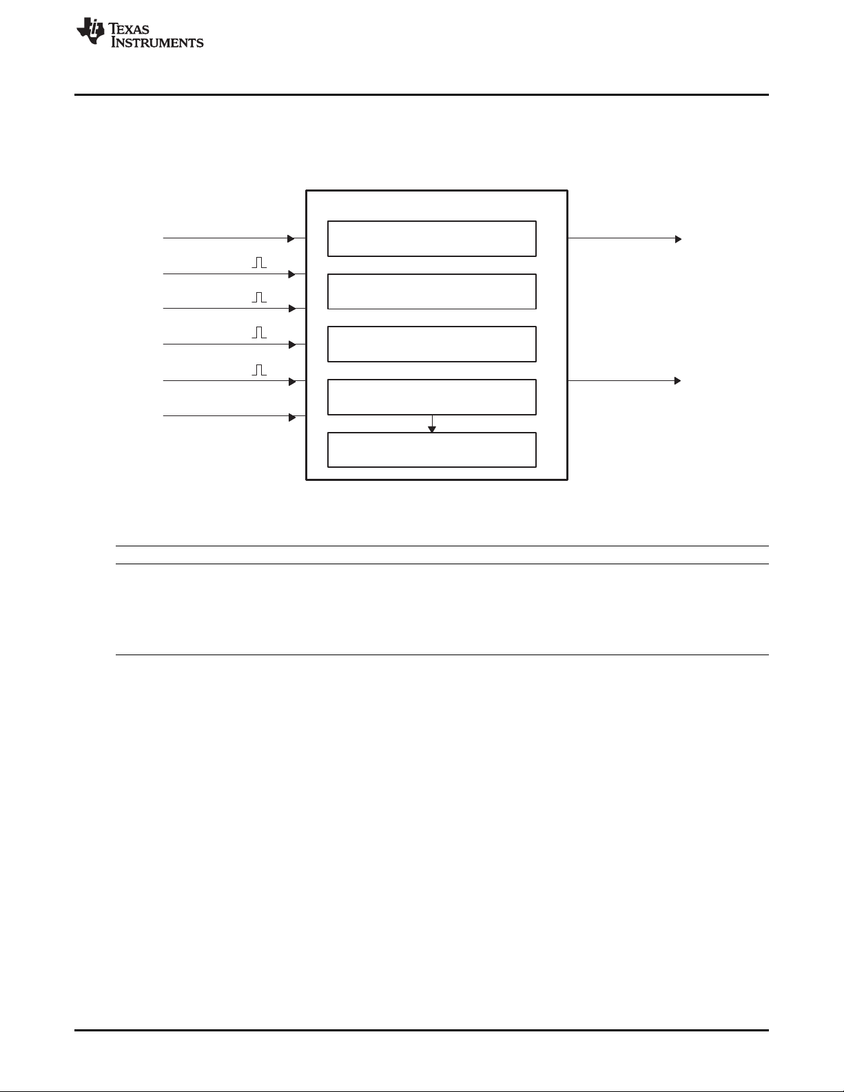
Action-qualifier(AQ)Module
AQCTLA[15:0]
Action-qualifiercontrolA
EPWMA
EPWMB
TBCLK
CTR=PRD
CTR=Zero
CTR=CMPA
CTR=CMPB
CTR_dir
AQCTLB[15:0]
Action-qualifiercontrolB
AQSFRC[15:0]
Action-qualifierS/Wforce
AQCSFRC[3:0](shadow)
continuousS/Wforce
AQCSFRC[3:0](active)
continuousS/Wforce
www.ti.com
The action-qualifier submodule is based on event-driven logic. It can be thought of as a programmable
cross switch with events at the input and actions at the output, all of which are software controlled via the
set of registers shown in Table 7.
ePWM Submodules
Figure 21. Action-Qualifier Submodule Inputs and Outputs
For convenience, the possible input events are summarized again in Table 8.
Table 8. Action-Qualifier Submodule Possible Input Events
Signal Description Registers Compared
CTR = PRD Time-base counter equal to the period value TBCTR = TBPRD
CTR = Zero Time-base counter equal to zero TBCTR = 0x0000
CTR = CMPA Time-base counter equal to the counter-compare A TBCTR = CMPA
CTR = CMPB Time-base counter equal to the counter-compare B TBCTR = CMPB
Software forced event Asynchronous event initiated by software
The software forced action is a useful asynchronous event. This control is handled by registers AQSFRC
and AQCSFRC.
The action-qualifier submodule controls how the two outputs EPWMxA and EPWMxB behave when a
particular event occurs. The event inputs to the action-qualifier submodule are further qualified by the
counter direction (up or down). This allows for independent action on outputs on both the count-up and
count-down phases.
The possible actions imposed on outputs EPWMxA and EPWMxB are:
• Set High:
Set output EPWMxA or EPWMxB to a high level.
• Clear Low:
Set output EPWMxA or EPWMxB to a low level.
• Toggle:
If EPWMxA or EPWMxB is currently pulled high, then pull the output low. If EPWMxA or EPWMxB is
currently pulled low, then pull the output high.
• Do Nothing:
Keep outputs EPWMxA and EPWMxB at same level as currently set. Although the "Do Nothing" option
prevents an event from causing an action on the EPWMxA and EPWMxB outputs, this event can still
trigger interrupts and ADC start of conversion. See the Event-trigger Submodule description in
Section 2.8 for details.
SPRUG04A–October 2008–Revised July 2009 TMS320x2833x, 2823x Enhanced Pulse Width Modulator (ePWM) Module
Submit Documentation Feedback
© 2008–2009, Texas Instruments Incorporated
39
Page 40
Z
Z
Z
CA
CA
CA
Z
T
CB
T
P
T
CA
T
CB P
CB
CB P
Do Nothing
Clear Low
Set High
Toggle
P
Zero
Comp
A
Comp
B
Period
TB Counter equals:
Actions
S/W
force
SW
SW
SW
SW
T
ePWM Submodules
Actions are specified independently for either output (EPWMxA or EPWMxB). Any or all events can be
configured to generate actions on a given output. For example, both CTR = CMPA and CTR = CMPB can
operate on output EPWMxA. All qualifier actions are configured via the control registers found at the end
of this section.
For clarity, the drawings in this document use a set of symbolic actions. These symbols are summarized in
Figure 22. Each symbol represents an action as a marker in time. Some actions are fixed in time (zero
and period) while the CMPA and CMPB actions are moveable and their time positions are programmed
via the counter-compare A and B registers, respectively. To turn off or disable an action, use the "Do
Nothing option"; it is the default at reset.
Figure 22. Possible Action-Qualifier Actions for EPWMxA and EPWMxB Outputs
www.ti.com
40
TMS320x2833x, 2823x Enhanced Pulse Width Modulator (ePWM) Module SPRUG04A–October 2008–Revised July 2009
© 2008–2009, Texas Instruments Incorporated
Submit Documentation Feedback
Page 41

www.ti.com
2.4.3 Action-Qualifier Event Priority
It is possible for the ePWM action qualifier to receive more than one event at the same time. In this case
events are assigned a priority by the hardware. The general rule is events occurring later in time have a
higher priority and software forced events always have the highest priority. The event priority levels for
up-down-count mode are shown in Table 9. A priority level of 1 is the highest priority and level 7 is the
lowest. The priority changes slightly depending on the direction of TBCTR.
Table 9. Action-Qualifier Event Priority for Up-Down-Count Mode
Priority Level Event If TBCTR is Incrementing Event If TBCTR is Decrementing
TBCTR = Zero up to TBCTR = TBPRD TBCTR = TBPRD down to TBCTR = 1
1 (Highest) Software forced event Software forced event
2 Counter equals CMPB on up-count (CBU) Counter equals CMPB on down-count (CBD)
3 Counter equals CMPA on up-count (CAU) Counter equals CMPA on down-count (CAD)
4 Counter equals zero Counter equals period (TBPRD)
5 Counter equals CMPB on down-count (CBD) Counter equals CMPB on up-count (CBU)
6 (Lowest) Counter equals CMPA on down-count (CAD) Counter equals CMPA on up-count (CBU)
Table 10 shows the action-qualifier priority for up-count mode. In this case, the counter direction is always
defined as up and thus down-count events will never be taken.
Table 10. Action-Qualifier Event Priority for Up-Count Mode
Priority Level Event
1 (Highest) Software forced event
2 Counter equal to period (TBPRD)
3 Counter equal to CMPB on up-count (CBU)
4 Counter equal to CMPA on up-count (CAU)
5 (Lowest) Counter equal to Zero
ePWM Submodules
Table 11 shows the action-qualifier priority for down-count mode. In this case, the counter direction is
always defined as down and thus up-count events will never be taken.
Table 11. Action-Qualifier Event Priority for Down-Count Mode
Priority Level Event
1 (Highest) Software forced event
2 Counter equal to Zero
3 Counter equal to CMPB on down-count (CBD)
4 Counter equal to CMPA on down-count (CAD)
5 (Lowest) Counter equal to period (TBPRD)
It is possible to set the compare value greater than the period. In this case the action will take place as
shown in Table 12.
Table 12. Behavior if CMPA/CMPB is Greater than the Period
Counter Mode Compare on Up-Count Event Compare on Down-Count Event
Up-Count Mode If CMPA/CMPB ≤ TBPRD period, then the event Never occurs.
Down-Count Mode Never occurs. If CMPA/CMPB < TBPRD, the event will occur on a
CAD/CBD CAD/CBD
occurs on a compare match (TBCTR=CMPA or
CMPB).
If CMPA/CMPB > TBPRD, then the event will not
occur.
compare match (TBCTR=CMPA or CMPB).
If CMPA/CMPB ≥ TBPRD, the event will occur on a
period match (TBCTR=TBPRD).
SPRUG04A–October 2008–Revised July 2009 TMS320x2833x, 2823x Enhanced Pulse Width Modulator (ePWM) Module
Submit Documentation Feedback
© 2008–2009, Texas Instruments Incorporated
41
Page 42

ePWM Submodules
Table 12. Behavior if CMPA/CMPB is Greater than the Period (continued)
Counter Mode Compare on Up-Count Event Compare on Down-Count Event
CAD/CBD CAD/CBD
Up-Down-Count If CMPA/CMPB < TBPRD and the counter is If CMPA/CMPB < TBPRD and the counter is
Mode incrementing, the event occurs on a compare match decrementing, the event occurs on a compare match
(TBCTR=CMPA or CMPB). (TBCTR=CMPA or CMPB).
If CMPA/CMPB is ≥ TBPRD, the event will occur on a If CMPA/CMPB ≥ TBPRD, the event occurs on a
period match (TBCTR = TBPRD). period match (TBCTR=TBPRD).
2.4.4 Waveforms for Common Configurations
NOTE: The waveforms in this document show the ePWMs behavior for a static compare register
value. In a running system, the active compare registers (CMPA and CMPB) are typically
updated from their respective shadow registers once every period. The user specifies when
the update will take place; either when the time-base counter reaches zero or when the
time-base counter reaches period. There are some cases when the action based on the new
value can be delayed by one period or the action based on the old value can take effect for
an extra period. Some PWM configurations avoid this situation. These include, but are not
limited to, the following:
Use up-down-count mode to generate a symmetric PWM:
• If you load CMPA/CMPB on zero, then use CMPA/CMPB values greater
than or equal to 1.
• If you load CMPA/CMPB on period, then use CMPA/CMPB values less than
or equal to TBPRD-1.
This means there will always be a pulse of at least one TBCLK cycle in a
PWM period which, when very short, tend to be ignored by the system.
Use up-down-count mode to generate an asymmetric PWM:
• To achieve 50%-0% asymmetric PWM use the following configuration: Load
CMPA/CMPB on period and use the period action to clear the PWM and a
compare-up action to set the PWM. Modulate the compare value from 0 to
TBPRD to achieve 50%-0% PWM duty.
When using up-count mode to generate an asymmetric PWM:
• To achieve 0-100% asymmetric PWM use the following configuration: Load
CMPA/CMPB on TBPRD. Use the Zero action to set the PWM and a
compare-up action to clear the PWM. Modulate the compare value from 0 to
TBPRD+1 to achieve 0-100% PWM duty.
See the Using Enhanced Pulse Width Modulator (ePWM) Module for 0-100%
Duty Cycle Control Application Report (literature number SPRAAI1)
www.ti.com
42
Figure 23 shows how a symmetric PWM waveform can be generated using the up-down-count mode of
the TBCTR. In this mode 0%-100% DC modulation is achieved by using equal compare matches on the
up count and down count portions of the waveform. In the example shown, CMPA is used to make the
comparison. When the counter is incrementing the CMPA match will pull the PWM output high. Likewise,
when the counter is decrementing the compare match will pull the PWM signal low. When CMPA = 0, the
PWM signal is low for the entire period giving the 0% duty waveform. When CMPA = TBPRD, the PWM
signal is high achieving 100% duty.
When using this configuration in practice, if you load CMPA/CMPB on zero, then use CMPA/CMPB values
greater than or equal to 1. If you load CMPA/CMPB on period, then use CMPA/CMPB values less than or
equal to TBPRD-1. This means there will always be a pulse of at least one TBCLK cycle in a PWM period
which, when very short, tend to be ignored by the system.
TMS320x2833x, 2823x Enhanced Pulse Width Modulator (ePWM) Module SPRUG04A–October 2008–Revised July 2009
Submit Documentation Feedback
© 2008–2009, Texas Instruments Incorporated
Page 43

UP
DOWN
UP
DOWN
2
0
3
4
1
2
3
1
2
0
3
4
1
2
0
3
1
TBCTR
TBCTRDirection
EPWMxA/EPWMxB
Case2:
CMPA =3,25%Duty
Case3:
CMPA =2,50%Duty
Case3:
CMPA =1,75%Duty
Case4:
CMPA =0,100%Duty
Case1:
CMPA =4,0%Duty
EPWMxA/EPWMxB
EPWMxA/EPWMxB
EPWMxA/EPWMxB
EPWMxA/EPWMxB
Mode:Up-DownCount
TBPRD=4
CAU=SET,CAD=CLEAR
0%-100%Duty
www.ti.com
ePWM Submodules
Figure 23. Up-Down-Count Mode Symmetrical Waveform
The PWM waveforms in Figure 24 through Figure 29 show some common action-qualifier configurations.
The C-code samples in Example 2 through Example 7 shows how to configure an ePWM module for each
case. Some conventions used in the figures and examples are as follows:
• TBPRD, CMPA, and CMPB refer to the value written in their respective registers. The active register,
not the shadow register, is used by the hardware.
• CMPx, refers to either CMPA or CMPB.
• EPWMxA and EPWMxB refer to the output signals from ePWMx
• Up-Down means Count-up-and-down mode, Up means up-count mode and Dwn means down-count
mode
• Sym = Symmetric, Asym = Asymmetric
SPRUG04A–October 2008–Revised July 2009 TMS320x2833x, 2823x Enhanced Pulse Width Modulator (ePWM) Module
Submit Documentation Feedback
© 2008–2009, Texas Instruments Incorporated
43
Page 44

TBCTR
EPWMxB
TBPRD
value
CAZ P CB Z P CB CA Z P
Z P CA Z P CA Z PCBCB
ePWM Submodules
Figure 24. Up, Single Edge Asymmetric Waveform, With Independent Modulation on EPWMxA and
EPWMxB—Active High
www.ti.com
A PWM period = (TBPRD + 1 ) × T
B Duty modulation for EPWMxA is set by CMPA, and is active high (that is, high time duty proportional to CMPA).
C Duty modulation for EPWMxB is set by CMPB and is active high (that is, high time duty proportional to CMPB).
D The "Do Nothing" actions ( X ) are shown for completeness, but will not be shown on subsequent diagrams.
E Actions at zero and period, although appearing to occur concurrently, are actually separated by one TBCLK period.
TBCTR wraps from period to 0000.
TBCLK
Example 2 contains a code sample showing initialization and run time for the waveforms in Figure 24.
Example 2. Code Sample for Figure 24
// Initialization Time
// = = = = = = = = = = = = = = = = = = = = = = = =
EPwm1Regs.TBPRD = 600; // Period = 601 TBCLK counts
EPwm1Regs.CMPA.half.CMPA = 350; // Compare A = 350 TBCLK counts
EPwm1Regs.CMPB = 200; // Compare B = 200 TBCLK counts
EPwm1Regs.TBPHS = 0; // Set Phase register to zero
EPwm1Regs.TBCTR = 0; // clear TB counter
EPwm1Regs.TBCTL.bit.CTRMODE = TB_COUNT_UP;
EPwm1Regs.TBCTL.bit.PHSEN = TB_DISABLE; // Phase loading disabled
EPwm1Regs.TBCTL.bit.PRDLD = TB_SHADOW;
EPwm1Regs.TBCTL.bit.SYNCOSEL = TB_SYNC_DISABLE;
EPwm1Regs.TBCTL.bit.HSPCLKDIV = TB_DIV1; // TBCLK = SYSCLK
EPwm1Regs.TBCTL.bit.CLKDIV = TB_DIV1;
EPwm1Regs.CMPCTL.bit.SHDWAMODE = CC_SHADOW;
EPwm1Regs.CMPCTL.bit.SHDWBMODE = CC_SHADOW;
EPwm1Regs.CMPCTL.bit.LOADAMODE = CC_CTR_ZERO; // load on CTR = Zero
EPwm1Regs.CMPCTL.bit.LOADBMODE = CC_CTR_ZERO; // load on CTR = Zero
EPwm1Regs.AQCTLA.bit.ZRO = AQ_SET;
EPwm1Regs.AQCTLA.bit.CAU = AQ_CLEAR;
EPwm1Regs.AQCTLB.bit.ZRO = AQ_SET;
EPwm1Regs.AQCTLB.bit.CBU = AQ_CLEAR;
//
// Run Time
// = = = = = = = = = = = = = = = = = = = = = = = =
EPwm1Regs.CMPA.half.CMPA = Duty1A; // adjust duty for output EPWM1A
EPwm1Regs.CMPB = Duty1B; // adjust duty for output EPWM1B
44
TMS320x2833x, 2823x Enhanced Pulse Width Modulator (ePWM) Module SPRUG04A–October 2008–Revised July 2009
© 2008–2009, Texas Instruments Incorporated
Submit Documentation Feedback
Page 45

TBCTR
EPWMxB
TBPRD
value
CB
CAP
P P
P
CB
CA
P
P
www.ti.com
ePWM Submodules
Figure 25. Up, Single Edge Asymmetric Waveform With Independent Modulation on EPWMxA and
EPWMxB—Active Low
A PWM period = (TBPRD + 1 ) × T
B Duty modulation for EPWMxA is set by CMPA, and is active low (that is, the low time duty is proportional to CMPA).
C Duty modulation for EPWMxB is set by CMPB and is active low (that is, the low time duty is proportional to CMPB).
D Actions at zero and period, although appearing to occur concurrently, are actually separated by one TBCLK period.
TBCTR wraps from period to 0000.
TBCLK
Example 3 contains a code sample showing initialization and run time for the waveforms in Figure 25.
SPRUG04A–October 2008–Revised July 2009 TMS320x2833x, 2823x Enhanced Pulse Width Modulator (ePWM) Module
Submit Documentation Feedback
© 2008–2009, Texas Instruments Incorporated
45
Page 46

TBCTR
EPWMxB
TBPRD
value
CA
T
Z
T
Z
T
Z
CA
CB
CB
ePWM Submodules
Example 3. Code Sample for Figure 25
// Initialization Time
// = = = = = = = = = = = = = = = = = = = = = = = =
EPwm1Regs.TBPRD = 600; // Period = 601 TBCLK counts
EPwm1Regs.CMPA.half.CMPA = 350; // Compare A = 350 TBCLK counts
EPwm1Regs.CMPB = 200; // Compare B = 200 TBCLK counts
EPwm1Regs.TBPHS = 0; // Set Phase register to zero
EPwm1Regs.TBCTR = 0; // clear TB counter
EPwm1Regs.TBCTL.bit.CTRMODE = TB_COUNT_UP;
EPwm1Regs.TBCTL.bit.PHSEN = TB_DISABLE; // Phase loading disabled
EPwm1Regs.TBCTL.bit.PRDLD = TB_SHADOW;
EPwm1Regs.TBCTL.bit.SYNCOSEL = TB_SYNC_DISABLE;
EPwm1Regs.TBCTL.bit.HSPCLKDIV = TB_DIV1; // TBCLK = SYSCLKOUT
EPwm1Regs.TBCTL.bit.CLKDIV = TB_DIV1;
EPwm1Regs.CMPCTL.bit.SHDWAMODE = CC_SHADOW;
EPwm1Regs.CMPCTL.bit.SHDWBMODE = CC_SHADOW;
EPwm1Regs.CMPCTL.bit.LOADAMODE = CC_CTR_ZERO; // load on TBCTR = Zero
EPwm1Regs.CMPCTL.bit.LOADBMODE = CC_CTR_ZERO; // load on TBCTR = Zero
EPwm1Regs.AQCTLA.bit.PRD = AQ_CLEAR;
EPwm1Regs.AQCTLA.bit.CAU = AQ_SET;
EPwm1Regs.AQCTLB.bit.PRD = AQ_CLEAR;
EPwm1Regs.AQCTLB.bit.CBU = AQ_SET;
//
// Run Time
// = = = = = = = = = = = = = = = = = = = = = = = =
EPwm1Regs.CMPA.half.CMPA = Duty1A; // adjust duty for output EPWM1A
EPwm1Regs.CMPB = Duty1B; // adjust duty for output EPWM1B
www.ti.com
Figure 26. Up-Count, Pulse Placement Asymmetric Waveform With Independent Modulation on EPWMxA
A PWM frequency = 1/( (TBPRD + 1 ) × T
B Pulse can be placed anywhere within the PWM cycle (0000 - TBPRD)
C High time duty proportional to (CMPB - CMPA)
D EPWMxB can be used to generate a 50% duty square wave with frequency = × ( (TBPRD + 1 ) × TBCLK )
TBCLK
)
Example 4 contains a code sample showing initialization and run time for the waveforms Figure 26. Use
the code in to define the headers.
46
TMS320x2833x, 2823x Enhanced Pulse Width Modulator (ePWM) Module SPRUG04A–October 2008–Revised July 2009
© 2008–2009, Texas Instruments Incorporated
Submit Documentation Feedback
Page 47

www.ti.com
Example 4. Code Sample for Figure 26
// Initialization Time
// = = = = = = = = = = = = = = = = = = = = = = = =
EPwm1Regs.TBPRD = 600; // Period = 601 TBCLK counts
EPwm1Regs.CMPA.half.CMPA = 200; // Compare A = 200 TBCLK counts
EPwm1Regs.CMPB = 400; // Compare B = 400 TBCLK counts
EPwm1Regs.TBPHS = 0; // Set Phase register to zero
EPwm1Regs.TBCTR = 0; // clear TB counter
EPwm1Regs.TBCTL.bit.CTRMODE = TB_COUNT_UP;
EPwm1Regs.TBCTL.bit.PHSEN = TB_DISABLE; // Phase loading disabled
EPwm1Regs.TBCTL.bit.PRDLD = TB_SHADOW;
EPwm1Regs.TBCTL.bit.SYNCOSEL = TB_SYNC_DISABLE;
EPwm1Regs.TBCTL.bit.HSPCLKDIV = TB_DIV1; // TBCLK = SYSCLKOUT
EPwm1Regs.TBCTL.bit.CLKDIV = TB_DIV1;
EPwm1Regs.CMPCTL.bit.SHDWAMODE = CC_SHADOW;
EPwm1Regs.CMPCTL.bit.SHDWBMODE = CC_SHADOW;
EPwm1Regs.CMPCTL.bit.LOADAMODE = CC_CTR_ZERO; // load on TBCTR = Zero
EPwm1Regs.CMPCTL.bit.LOADBMODE = CC_CTR_ZERO; // load on TBCTR = Zero
EPwm1Regs.AQCTLA.bit.CAU = AQ_SET;
EPwm1Regs.AQCTLA.bit.CBU = AQ_CLEAR;
EPwm1Regs.AQCTLB.bit.ZRO = AQ_TOGGLE;
//
// Run Time
// = = = = = = = = = = = = = = = = = = = = = = = =
EPwm1Regs.CMPA.half.CMPA = EdgePosA; // adjust duty for output EPWM1A only
EPwm1Regs.CMPB = EdgePosB;
ePWM Submodules
SPRUG04A–October 2008–Revised July 2009 TMS320x2833x, 2823x Enhanced Pulse Width Modulator (ePWM) Module
Submit Documentation Feedback
© 2008–2009, Texas Instruments Incorporated
47
Page 48
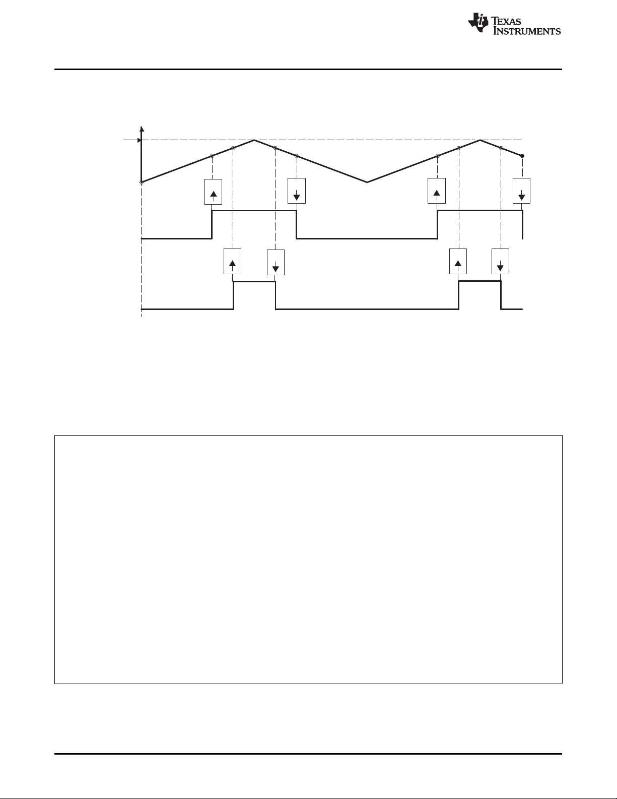
TBCTR
EPWMxA
EPWMxB
TBPRD
value
CA
CA
CA
CA
CBCB
CB
CB
CB
ePWM Submodules
www.ti.com
Figure 27. Up-Down-Count, Dual Edge Symmetric Waveform, With Independent Modulation on EPWMxA
and EPWMxB — Active Low
A PWM period = 2 x TBPRD × T
B Duty modulation for EPWMxA is set by CMPA, and is active low (that is, the low time duty is proportional to CMPA).
C Duty modulation for EPWMxB is set by CMPB and is active low (that is, the low time duty is proportional to CMPB).
D Outputs EPWMxA and EPWMxB can drive independent power switches
TBCLK
Example 5 contains a code sample showing initialization and run time for the waveforms in Figure 27. Use
the code in to define the headers.
Example 5. Code Sample for Figure 27
// Initialization Time
// = = = = = = = = = = = = = = = = = = = = = = = =
EPwm1Regs.TBPRD = 600; // Period = 2´600 TBCLK counts
EPwm1Regs.CMPA.half.CMPA = 400; // Compare A = 400 TBCLK counts
EPwm1Regs.CMPB = 500; // Compare B = 500 TBCLK counts
EPwm1Regs.TBPHS = 0; // Set Phase register to zero
EPwm1Regs.TBCTR = 0; // clear TB counter
EPwm1Regs.TBCTL.bit.CTRMODE = TB_COUNT_UPDOWN; // Symmetric
xEPwm1Regs.TBCTL.bit.PHSEN = TB_DISABLE; // Phase loading disabled
xEPwm1Regs.TBCTL.bit.PRDLD = TB_SHADOW;
EPwm1Regs.TBCTL.bit.SYNCOSEL = TB_SYNC_DISABLE;
EPwm1Regs.TBCTL.bit.HSPCLKDIV = TB_DIV1; // TBCLK = SYSCLKOUT
EPwm1Regs.TBCTL.bit.CLKDIV = TB_DIV1;
EPwm1Regs.CMPCTL.bit.SHDWAMODE = CC_SHADOW;
EPwm1Regs.CMPCTL.bit.SHDWBMODE = CC_SHADOW;
EPwm1Regs.CMPCTL.bit.LOADAMODE = CC_CTR_ZERO; // load on CTR = Zero
EPwm1Regs.CMPCTL.bit.LOADBMODE = CC_CTR_ZERO; // load on CTR = Zero
EPwm1Regs.AQCTLA.bit.CAU = AQ_SET;
EPwm1Regs.AQCTLA.bit.CAD = AQ_CLEAR;
EPwm1Regs.AQCTLB.bit.CBU = AQ_SET;
EPwm1Regs.AQCTLB.bit.CBD = AQ_CLEAR;
//
// Run Time
// = = = = = = = = = = = = = = = = = = = = = = = =
EPwm1Regs.CMPA.half.CMPA = Duty1A; // adjust duty for output EPWM1A
EPwm1Regs.CMPB = Duty1B; // adjust duty for output EPWM1B
48
TMS320x2833x, 2823x Enhanced Pulse Width Modulator (ePWM) Module SPRUG04A–October 2008–Revised July 2009
© 2008–2009, Texas Instruments Incorporated
Submit Documentation Feedback
Page 49

CA CA CA
CA
CB CB
CB
CB
TBCTR
EPWMxA
EPWMxB
TBPRD
value
www.ti.com
ePWM Submodules
Figure 28. Up-Down-Count, Dual Edge Symmetric Waveform, With Independent Modulation on EPWMxA
and EPWMxB — Complementary
A PWM period = 2 × TBPRD × T
B Duty modulation for EPWMxA is set by CMPA, and is active low, i.e., low time duty proportional to CMPA
C Duty modulation for EPWMxB is set by CMPB and is active high, i.e., high time duty proportional to CMPB
D Outputs EPWMx can drive upper/lower (complementary) power switches
E Dead-band = CMPB - CMPA (fully programmable edge placement by software). Note the dead-band module is also
available if the more classical edge delay method is required.
TBCLK
Example 6 contains a code sample showing initialization and run time for the waveforms in Figure 28. Use
the code in to define the headers.
Example 6. Code Sample for Figure 28
// Initialization Time
// = = = = = = = = = = = = = = = = = = = = = = = =
EPwm1Regs.TBPRD = 600; // Period = 2´600 TBCLK counts
EPwm1Regs.CMPA.half.CMPA = 350; // Compare A = 350 TBCLK counts
EPwm1Regs.CMPB = 400; // Compare B = 400 TBCLK counts
EPwm1Regs.TBPHS = 0; // Set Phase register to zero
EPwm1Regs.TBCTR = 0; // clear TB counter
EPwm1Regs.TBCTL.bit.CTRMODE = TB_COUNT_UPDOWN; // Symmetric
EPwm1Regs.TBCTL.bit.PHSEN = TB_DISABLE; // Phase loading disabled
EPwm1Regs.TBCTL.bit.PRDLD = TB_SHADOW;
EPwm1Regs.TBCTL.bit.SYNCOSEL = TB_SYNC_DISABLE;
EPwm1Regs.TBCTL.bit.HSPCLKDIV = TB_DIV1; // TBCLK = SYSCLKOUT
EPwm1Regs.TBCTL.bit.CLKDIV = TB_DIV1;
EPwm1Regs.CMPCTL.bit.SHDWAMODE = CC_SHADOW;
EPwm1Regs.CMPCTL.bit.SHDWBMODE = CC_SHADOW;
EPwm1Regs.CMPCTL.bit.LOADAMODE = CC_CTR_ZERO; // load on CTR = Zero
EPwm1Regs.CMPCTL.bit.LOADBMODE = CC_CTR_ZERO; // load on CTR = Zero
EPwm1Regs.AQCTLA.bit.CAU = AQ_SET;
EPwm1Regs.AQCTLA.bit.CAD = AQ_CLEAR;
EPwm1Regs.AQCTLB.bit.CBU = AQ_CLEAR;
EPwm1Regs.AQCTLB.bit.CBD = AQ_SET;
// Run Time
// = = = = = = = = = = = = = = = = = = = = = = = =
EPwm1Regs.CMPA.half.CMPA = Duty1A; // adjust duty for output EPWM1A
EPwm1Regs.CMPB = Duty1B; // adjust duty for output EPWM1B
SPRUG04A–October 2008–Revised July 2009 TMS320x2833x, 2823x Enhanced Pulse Width Modulator (ePWM) Module
Submit Documentation Feedback
© 2008–2009, Texas Instruments Incorporated
49
Page 50
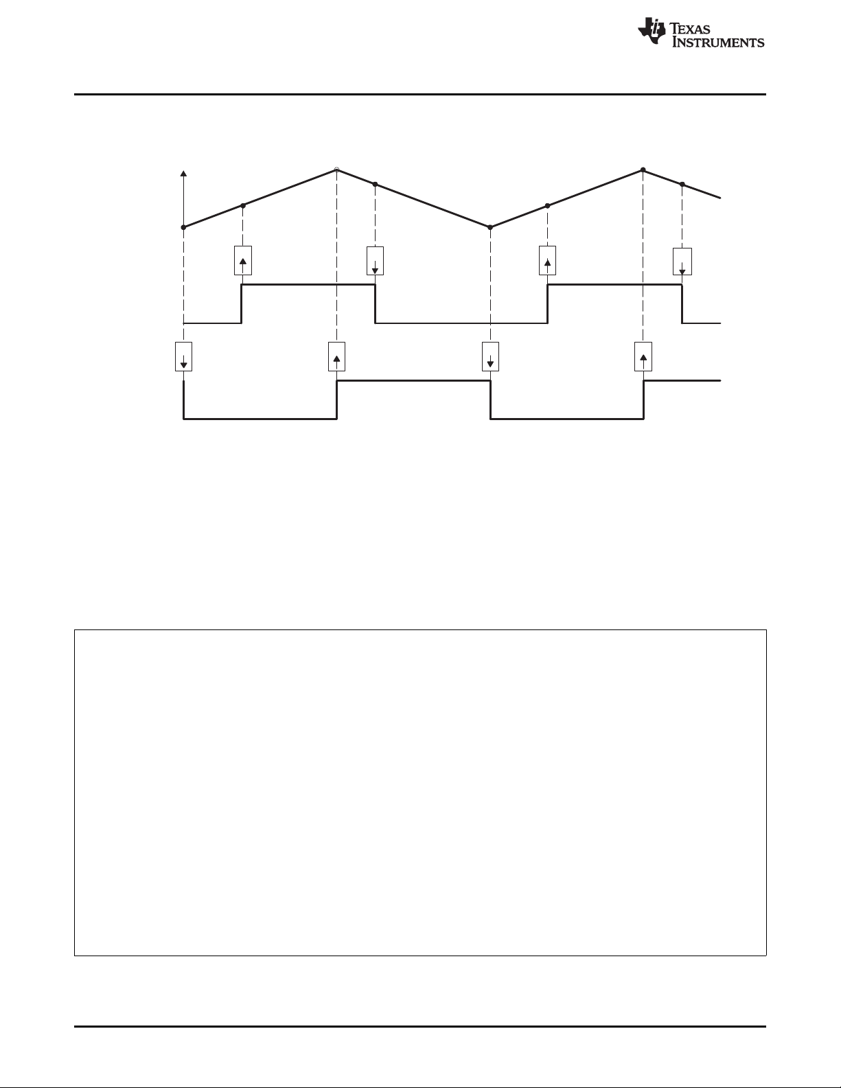
Z P Z P
TBCTR
EPWMxA
CA CA
CB
CB
ePWM Submodules
Figure 29. Up-Down-Count, Dual Edge Asymmetric Waveform, With Independent Modulation on
EPWMxA—Active Low
A PWM period = 2 × TBPRD × TBCLK
B Rising edge and falling edge can be asymmetrically positioned within a PWM cycle. This allows for pulse placement
techniques.
C Duty modulation for EPWMxA is set by CMPA and CMPB.
D Low time duty for EPWMxA is proportional to (CMPA + CMPB).
E To change this example to active high, CMPA and CMPB actions need to be inverted (i.e., Set ! Clear and Clear Set).
F Duty modulation for EPWMxB is fixed at 50% (utilizes spare action resources for EPWMxB)
Example 7 contains a code sample showing initialization and run time for the waveforms in Figure 29. Use
the code in to define the headers.
www.ti.com
Example 7. Code Sample for Figure 29
// Initialization Time
// = = = = = = = = = = = = = = = = = = = = = = = =
EPwm1Regs.TBPRD = 600; // Period = 2 ´ 600 TBCLK counts
EPwm1Regs.CMPA.half.CMPA = 250; // Compare A = 250 TBCLK counts
EPwm1Regs.CMPB = 450; // Compare B = 450 TBCLK counts
EPwm1Regs.TBPHS = 0; // Set Phase register to zero
EPwm1Regs.TBCTR = 0; // clear TB counter
EPwm1Regs.TBCTL.bit.CTRMODE = TB_COUNT_UPDOWN; // Symmetric
EPwm1Regs.TBCTL.bit.PHSEN = TB_DISABLE; // Phase loading disabled
EPwm1Regs.TBCTL.bit.PRDLD = TB_SHADOW;
EPwm1Regs.TBCTL.bit.SYNCOSEL = TB_SYNC_DISABLE;
EPwm1Regs.TBCTL.bit.HSPCLKDIV = TB_DIV1; // TBCLK = SYSCLKOUT
EPwm1Regs.TBCTL.bit.CLKDIV = TB_DIV1;
EPwm1Regs.CMPCTL.bit.SHDWAMODE = CC_SHADOW;
EPwm1Regs.CMPCTL.bit.SHDWBMODE = CC_SHADOW;
EPwm1Regs.CMPCTL.bit.LOADAMODE = CC_CTR_ZERO; // load on CTR = Zero
EPwm1Regs.CMPCTL.bit.LOADBMODE = CC_CTR_ZERO; // load on CTR = Zero
EPwm1Regs.AQCTLA.bit.CAU = AQ_SET;
EPwm1Regs.AQCTLA.bit.CBD = AQ_CLEAR;
EPwm1Regs.AQCTLB.bit.ZRO = AQ_CLEAR;
EPwm1Regs.AQCTLB.bit.PRD = AQ_SET;
// Run Time
// = = = = = = = = = = = = = = = = = = = = = = = =
EPwm1Regs.CMPA.half.CMPA = EdgePosA; // adjust duty for output EPWM1A only
EPwm1Regs.CMPB = EdgePosB;
50
TMS320x2833x, 2823x Enhanced Pulse Width Modulator (ePWM) Module SPRUG04A–October 2008–Revised July 2009
© 2008–2009, Texas Instruments Incorporated
Submit Documentation Feedback
Page 51

CTR = CMPB
CTR = CMPA
CTR_Dir
CTR = 0
CTR = PRD
Dead
Band
(DB)
Counter
Compare
(CC)
Action
Qualifier
(AQ)
EPWMxA
EPWMxB
CTR = CMPB
CTR = 0
EPWMxINT
EPWMxSOCA
EPWMxSOCB
EPWMxA
EPWMxB
TZ1 to TZ6
CTR = CMPA
Time-Base
(TB)
CTR = PRD
CTR = 0
CTR_Dir
EPWMxSYNCI
EPWMxSYNCO
EPWMxTZINT
PWM-
chopper
(PC)
Event
Trigger
and
Interrupt
(ET)
Trip
Zone
(TZ)
GPIO
MUX
ADC
PIE
PIE
www.ti.com
2.5 Dead-Band Generator (DB) Submodule
Figure 30 illustrates the dead-band submodule within the ePWM module.
Figure 30. Dead_Band Submodule
ePWM Submodules
2.5.1 Purpose of the Dead-Band Submodule
The "Action-qualifier (AQ) Module" section discussed how it is possible to generate the required
dead-band by having full control over edge placement using both the CMPA and CMPB resources of the
ePWM module. However, if the more classical edge delay-based dead-band with polarity control is
required, then the dead-band submodule described here should be used.
The key functions of the dead-band module are:
• Generating appropriate signal pairs (EPWMxA and EPWMxB) with dead-band relationship from a
single EPWMxA input
• Programming signal pairs for:
– Active high (AH)
– Active low (AL)
– Active high complementary (AHC)
– Active low complementary (ALC)
• Adding programmable delay to rising edges (RED)
• Adding programmable delay to falling edges (FED)
• Can be totally bypassed from the signal path (note dotted lines in diagram)
2.5.2 Controlling and Monitoring the Dead-Band Submodule
The dead-band submodule operation is controlled and monitored via the following registers:
Table 13. Dead-Band Generator Submodule Registers
Register Name Address offset Shadowed Description
DBCTL 0x000F No Dead-Band Control Register
DBRED 0x0010 No Dead-Band Rising Edge Delay Count Register
DBFED 0x0011 No Dead-Band Falling Edge Delay Count Register
SPRUG04A–October 2008–Revised July 2009 TMS320x2833x, 2823x Enhanced Pulse Width Modulator (ePWM) Module
Submit Documentation Feedback
© 2008–2009, Texas Instruments Incorporated
51
Page 52

0
1
S2
1
0
S1
RED
OutIn
Risingedge
delay
(10-bit
counter)
(10-bit
counter)
delay
Fallingedge
In Out
FED
1
0
S3
0
S0
1
EPWMxA
EPWMxB
DBCTL[POLSEL] DBCTL[OUT_MODE]
S5
DBCTL[IN_MODE]
1
0
S4
0
1
EPWMxA in
EPWMxBin
ePWM Submodules
2.5.3 Operational Highlights for the Dead-Band Submodule
The following sections provide the operational highlights.
The dead-band submodule has two groups of independent selection options as shown in Figure 31.
• Input Source Selection:
The input signals to the dead-band module are the EPWMxA and EPWMxB output signals from the
action-qualifier. In this section they will be referred to as EPWMxA In and EPWMxB In. Using the
DBCTL[IN_MODE) control bits, the signal source for each delay, falling-edge or rising-edge, can be
selected:
– EPWMxA In is the source for both falling-edge and rising-edge delay. This is the default mode.
– EPWMxA In is the source for falling-edge delay, EPWMxB In is the source for rising-edge delay.
– EPWMxA In is the source for rising edge delay, EPWMxB In is the source for falling-edge delay.
– EPWMxB In is the source for both falling-edge and rising-edge delay.
• Output Mode Control:
The output mode is configured by way of the DBCTL[OUT_MODE] bits. These bits determine if the
falling-edge delay, rising-edge delay, neither, or both are applied to the input signals.
• Polarity Control:
The polarity control (DBCTL[POLSEL]) allows you to specify whether the rising-edge delayed signal
and/or the falling-edge delayed signal is to be inverted before being sent out of the dead-band
submodule.
Figure 31. Configuration Options for the Dead-Band Submodule
www.ti.com
Although all combinations are supported, not all are typical usage modes. Table 14 documents some
classical dead-band configurations. These modes assume that the DBCTL[IN_MODE] is configured such
that EPWMxA In is the source for both falling-edge and rising-edge delay. Enhanced, or non-traditional
modes can be achieved by changing the input signal source. The modes shown in Table 14 fall into the
following categories:
• Mode 1: Bypass both falling-edge delay (FED) and rising-edge delay (RED)
• Mode 2-5: Classical Dead-Band Polarity Settings:
52
TMS320x2833x, 2823x Enhanced Pulse Width Modulator (ePWM) Module SPRUG04A–October 2008–Revised July 2009
Allows you to fully disable the dead-band submodule from the PWM signal path.
These represent typical polarity configurations that should address all the active high/low modes
required by available industry power switch gate drivers. The waveforms for these typical cases are
shown in Figure 32. Note that to generate equivalent waveforms to Figure 32, configure the
action-qualifier submodule to generate the signal as shown for EPWMxA.
© 2008–2009, Texas Instruments Incorporated
Submit Documentation Feedback
Page 53

Original
(outA)
Rising Edge
Delayed (RED)
Falling Edge
Delayed (FED)
Active High
(AHC)
Active Low
(ALC)
Active High
(AH)
Active Low
(AL)
RED
FED
Period
www.ti.com
• Mode 6: Bypass rising-edge-delay and Mode 7: Bypass falling-edge-delay
Figure 32 shows waveforms for typical cases where 0% < duty < 100%.
ePWM Submodules
Finally the last two entries in Table 14 show combinations where either the falling-edge-delay (FED) or
rising-edge-delay (RED) blocks are bypassed.
Table 14. Classical Dead-Band Operating Modes
Mode Mode Description
1 EPWMxA and EPWMxB Passed Through (No Delay) X X 0 0
2 Active High Complementary (AHC) 1 0 1 1
3 Active Low Complementary (ALC) 0 1 1 1
4 Active High (AH) 0 0 1 1
5 Active Low (AL) 1 1 1 1
EPWMxA Out = EPWMxA In (No Delay)
6 0 or 1 0 or 1 0 1
EPWMxB Out = EPWMxA In with Falling Edge Delay
EPWMxA Out = EPWMxA In with Rising Edge Delay
7 0 or 1 0 or 1 1 0
EPWMxB Out = EPWMxB In with No Delay
DBCTL[POLSEL] DBCTL[OUT_MODE]
S3 S2 S1 S0
Figure 32. Dead-Band Waveforms for Typical Cases (0% < Duty < 100%)
SPRUG04A–October 2008–Revised July 2009 TMS320x2833x, 2823x Enhanced Pulse Width Modulator (ePWM) Module
Submit Documentation Feedback
© 2008–2009, Texas Instruments Incorporated
53
Page 54

ePWM Submodules
The dead-band submodule supports independent values for rising-edge (RED) and falling-edge (FED)
delays. The amount of delay is programmed using the DBRED and DBFED registers. These are 10-bit
registers and their value represents the number of time-base clock, TBCLK, periods a signal edge is
delayed by. For example, the formula to calculate falling-edge-delay and rising-edge-delay are:
FED = DBFED × T
RED = DBRED × T
Where T
TBCLK
For convenience, delay values for various TBCLK options are shown in Table 15.
Dead-Band Value Dead-Band Delay in μS
DBFED, DBRED TBCLK = SYSCLKOUT/1 TBCLK = SYSCLKOUT /2 TBCLK = SYSCLKOUT/4
www.ti.com
TBCLK
TBCLK
is the period of TBCLK, the prescaled version of SYSCLKOUT.
Table 15. Dead-Band Delay Values in μS as a Function of DBFED and DBRED
1 0.01 μS 0.02 μS 0.04 μS
5 0.05 μS 0.10 μS 0.20 μS
10 0.10 μS 0.20 μS 0.40 μS
100 1.00 μS 2.00 μS 4.00 μS
200 2.00 μS 4.00 μS 8.00 μS
300 3.00 μS 6.00 μS 12.00 μS
400 4.00 μS 8.00 μS 16.00 μS
500 5.00 μS 10.00 μS 20.00 μS
600 6.00 μS 12.00 μS 24.00 μS
700 7.00 μS 14.00 μS 28.00 μS
800 8.00 μS 16.00 μS 32.00 μS
900 9.00 μS 18.00 μS 36.00 μS
1000 10.00 μS 20.00 μS 40.00 μS
54
TMS320x2833x, 2823x Enhanced Pulse Width Modulator (ePWM) Module SPRUG04A–October 2008–Revised July 2009
Submit Documentation Feedback
© 2008–2009, Texas Instruments Incorporated
Page 55
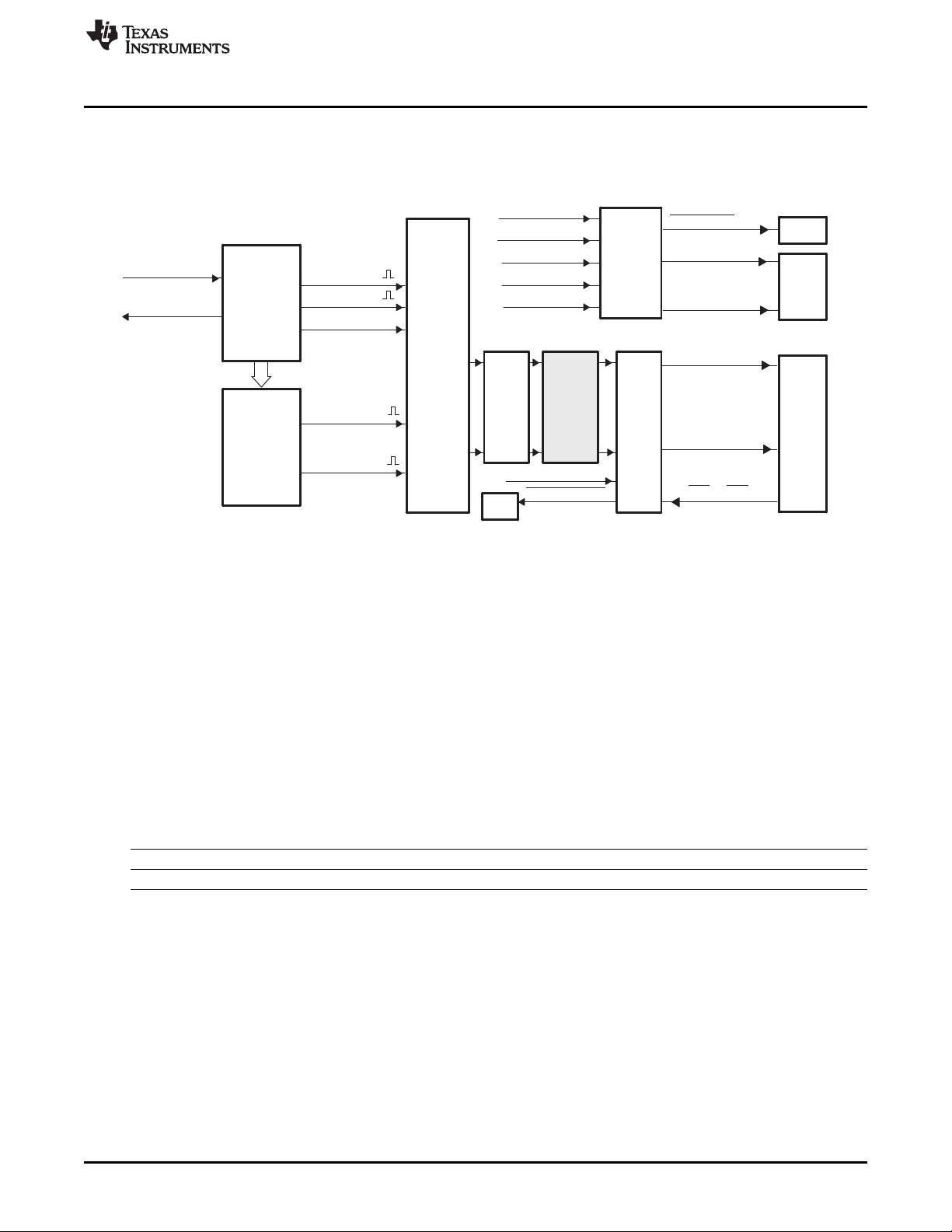
CTR = CMPB
CTR = CMPA
CTR_Dir
CTR = 0
CTR = PRD
Dead
Band
(DB)
Counter
Compare
(CC)
Action
Qualifier
(AQ)
EPWMxB
EPWMxA
CTR = CMPB
CTR = 0
EPWMxINT
EPWMxSOCA
EPWMxSOCB
EPWMxA
EPWMxB
TZ1 to TZ6
CTR = CMPA
Time-Base
(TB)
CTR = PRD
CTR = 0
CTR_Dir
EPWMxSYNCI
EPWMxSYNCO
EPWMxTZINT
PWM-
chopper
(PC)
Event
Trigger
and
Interrupt
(ET)
Trip
Zone
(TZ)
GPIO
MUX
ADC
PIE
PIE
www.ti.com
2.6 PWM-Chopper (PC) Submodule
Figure 33 illustrates the PWM-chopper (PC) submodule within the ePWM module.
Figure 33. PWM-Chopper Submodule
The PWM-chopper submodule allows a high-frequency carrier signal to modulate the PWM waveform
generated by the action-qualifier and dead-band submodules. This capability is important if you need
pulse transformer-based gate drivers to control the power switching elements.
ePWM Submodules
2.6.1 Purpose of the PWM-Chopper Submodule
The key functions of the PWM-chopper submodule are:
• Programmable chopping (carrier) frequency
• Programmable pulse width of first pulse
• Programmable duty cycle of second and subsequent pulses
• Can be fully bypassed if not required
2.6.2 Controlling the PWM-Chopper Submodule
The PWM-chopper submodule operation is controlled via the registers in Table 16.
Table 16. PWM-Chopper Submodule Registers
mnemonic Address offset Shadowed Description
PCCTL 0x001E No PWM-chopper Control Register
2.6.3 Operational Highlights for the PWM-Chopper Submodule
Figure 34 shows the operational details of the PWM-chopper submodule. The carrier clock is derived from
SYSCLKOUT. Its frequency and duty cycle are controlled via the CHPFREQ and CHPDUTY bits in the
PCCTL register. The one-shot block is a feature that provides a high energy first pulse to ensure hard and
fast power switch turn on, while the subsequent pulses sustain pulses, ensuring the power switch remains
on. The one-shot width is programmed via the OSHTWTH bits. The PWM-chopper submodule can be fully
disabled (bypassed) via the CHPEN bit.
SPRUG04A–October 2008–Revised July 2009 TMS320x2833x, 2823x Enhanced Pulse Width Modulator (ePWM) Module
Submit Documentation Feedback
© 2008–2009, Texas Instruments Incorporated
55
Page 56
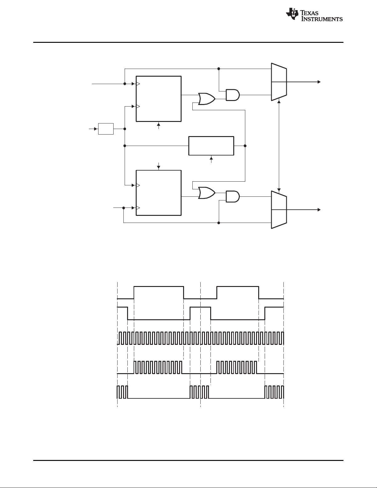
Start
Clk
One
shot
Pulse-width
PCCTL
[OSHTWTH]
PWMA_ch
Bypass
Dividerand
dutycontrol
PSCLK
OSHT
EPWMxA
PCCTL
[CHPEN]
EPWMxA
/8SYSCLKOUT
Pulse-width
Start
shot
Clk
One
PCCTL
[OSHTWTH]
1
OSHT
PCCTL[CHPFREQ]
PCCTL[CHPDUTY]
PWMB_ch
Bypass
EPWMxB
EPWMxB
1
0
0
PSCLK
ePWM Submodules
www.ti.com
Figure 34. PWM-Chopper Submodule Operational Details
2.6.4 Waveforms
Figure 35 shows simplified waveforms of the chopping action only; one-shot and duty-cycle control are not
shown. Details of the one-shot and duty-cycle control are discussed in the following sections.
Figure 35. Simple PWM-Chopper Submodule Waveforms Showing Chopping Action Only
56
TMS320x2833x, 2823x Enhanced Pulse Width Modulator (ePWM) Module SPRUG04A–October 2008–Revised July 2009
© 2008–2009, Texas Instruments Incorporated
Submit Documentation Feedback
Page 57

PSCLK
OSHT
EPWMxA in
Prog. pulse width
(OSHTWTH)
Start OSHT pulse
Sustaining pulses
www.ti.com
ePWM Submodules
2.6.4.1 One-Shot Pulse
The width of the first pulse can be programmed to any of 16 possible pulse width values. The width or
period of the first pulse is given by:
T
Where T
1stpulse
= T
SYSCLKOUT
SYSCLKOUT
× 8 × OSHTWTH
is the period of the system clock (SYSCLKOUT) and OSHTWTH is the four control bits
(value from 1 to 16)
Figure 36 shows the first and subsequent sustaining pulses and Table 7.3 gives the possible pulse width
values for a SYSCLKOUT = 100 MHz.
Figure 36. PWM-Chopper Submodule Waveforms Showing the First Pulse and Subsequent Sustaining
Pulses
Table 17. Possible Pulse Width Values for SYSCLKOUT
= 100 MHz
OSHTWTHz Pulse Width
(hex) (nS)
0 80
1 160
2 240
3 320
4 400
5 480
6 560
7 640
8 720
9 800
A 880
B 960
C 1040
D 1120
E 1200
F 1280
SPRUG04A–October 2008–Revised July 2009 TMS320x2833x, 2823x Enhanced Pulse Width Modulator (ePWM) Module
Submit Documentation Feedback
© 2008–2009, Texas Instruments Incorporated
57
Page 58

1/8
2/8
3/8
4/8
5/8
6/8
7/8
PSCLK
12.5%
25%
37.5%
50%
62.5%
75%
87.5%
PSCLK Period
PSCLK
period
ePWM Submodules
2.6.4.2 Duty Cycle Control
Pulse transformer-based gate drive designs need to comprehend the magnetic properties or
characteristics of the transformer and associated circuitry. Saturation is one such consideration. To assist
the gate drive designer, the duty cycles of the second and subsequent pulses have been made
programmable. These sustaining pulses ensure the correct drive strength and polarity is maintained on the
power switch gate during the on period, and hence a programmable duty cycle allows a design to be
tuned or optimized via software control.
Figure 37 shows the duty cycle control that is possible by programming the CHPDUTY bits. One of seven
possible duty ratios can be selected ranging from 12.5% to 87.5%.
Figure 37. PWM-Chopper Submodule Waveforms Showing the Pulse Width (Duty Cycle) Control of
Sustaining Pulses
www.ti.com
58
TMS320x2833x, 2823x Enhanced Pulse Width Modulator (ePWM) Module SPRUG04A–October 2008–Revised July 2009
Submit Documentation Feedback
© 2008–2009, Texas Instruments Incorporated
Page 59
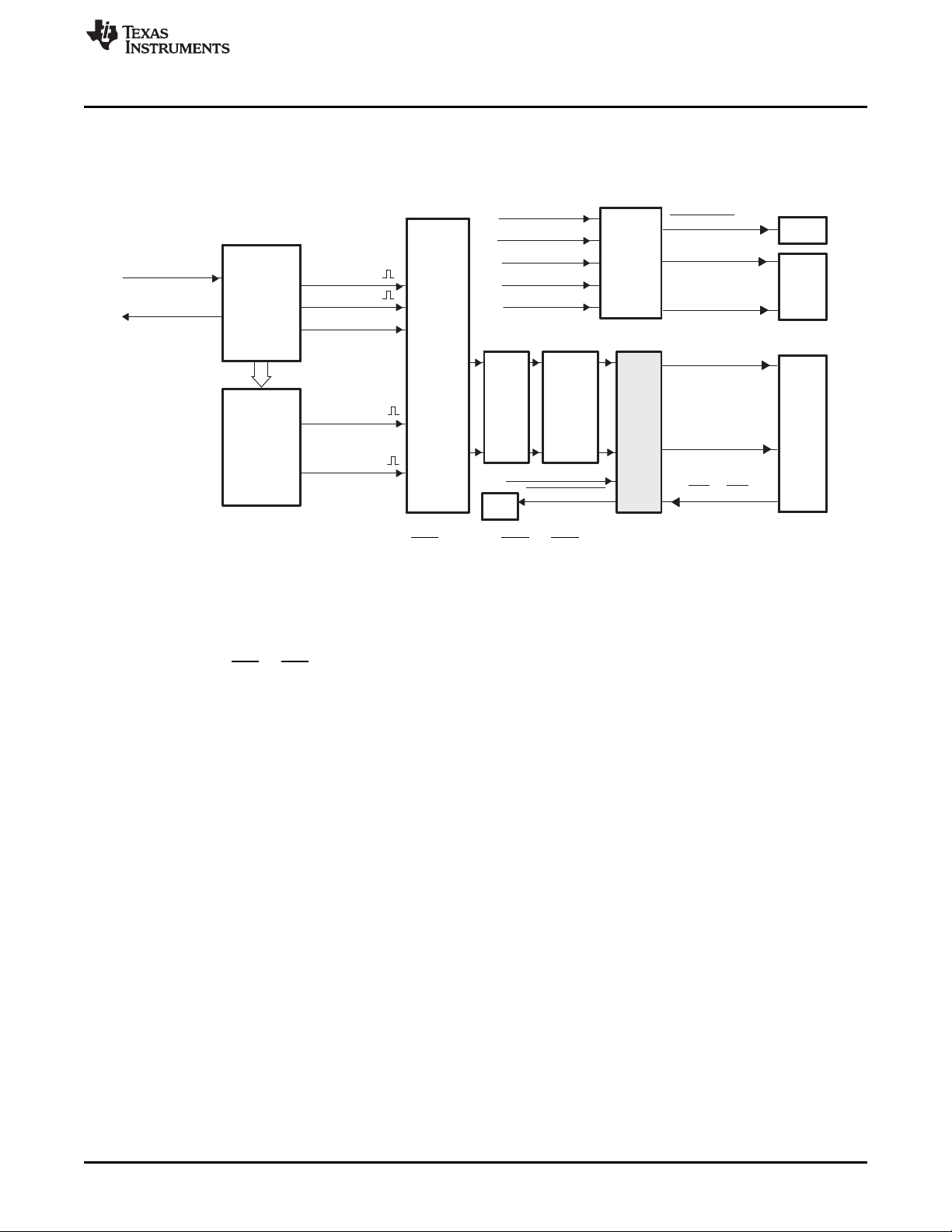
CTR = CMPB
CTR = CMPA
CTR_Dir
CTR = 0
CTR = PRD
Dead
Band
(DB)
Counter
Compare
(CC)
Action
Qualifier
(AQ)
EPWMxA
EPWMxB
CTR = CMPB
CTR = 0
EPWMxINT
EPWMxSOCA
EPWMxSOCB
EPWMxA
EPWMxB
TZ1 to TZ6
CTR = CMPA
Time-Base
(TB)
CTR = PRD
CTR = 0
CTR_Dir
EPWMxSYNCI
EPWMxSYNCO
EPWMxTZINT
PWM-
chopper
(PC)
Event
Trigger
and
Interrupt
(ET)
Trip
Zone
(TZ)
GPIO
MUX
ADC
PIE
PIE
www.ti.com
2.7 Trip-Zone (TZ) Submodule
Figure 38 shows how the trip-zone (TZ) submodule fits within the ePWM module.
Each ePWM module is connected to six TZn signals (TZ1 to TZ6) that are sourced from the GPIO MUX.
These signals indicate external fault or trip conditions, and the ePWM outputs can be programmed to
respond accordingly when faults occur.
ePWM Submodules
Figure 38. Trip-Zone Submodule
2.7.1 Purpose of the Trip-Zone Submodule
The key functions of the Trip-Zone submodule are:
• Trip inputs TZ1 to TZ6 can be flexibly mapped to any ePWM module.
• Upon a fault condition, outputs EPWMxA and EPWMxB can be forced to one of the following:
– High
– Low
– High-impedance
– No action taken
• Support for one-shot trip (OSHT) for major short circuits or over-current conditions.
• Support for cycle-by-cycle tripping (CBC) for current limiting operation.
• Each trip-zone input pin can be allocated to either one-shot or cycle-by-cycle operation.
• Interrupt generation is possible on any trip-zone pin .
• Software-forced tripping is also supported.
• The trip-zone submodule can be fully bypassed if it is not required.
SPRUG04A–October 2008–Revised July 2009 TMS320x2833x, 2823x Enhanced Pulse Width Modulator (ePWM) Module
Submit Documentation Feedback
© 2008–2009, Texas Instruments Incorporated
59
Page 60

ePWM Submodules
2.7.2 Controlling and Monitoring the Trip-Zone Submodule
The trip-zone submodule operation is controlled and monitored through the following registers:
Table 18. Trip-Zone Submodule Registers
Register Name Address offset Shadowed Description
TZSEL 0x0012 No Trip-Zone Select Register
reserved 0x0013
TZCTL 0x0014 No Trip-Zone Control Register
TZEINT 0x0015 No Trip-Zone Enable Interrupt Register
TZFLG 0x0016 No Trip-Zone Flag Register
TZCLR 0x0017 No Trip-Zone Clear Register
TZFRC 0x0018 No Trip-Zone Force Register
(1)
All trip-zone registers are EALLOW protected and can be modified only after executing the EALLOW instruction. For more
information, see the device-specific version of the System Control and Interrupts Reference Guide listed in Section 1.
2.7.3 Operational Highlights for the Trip-Zone Submodule
The following sections describe the operational highlights and configuration options for the trip-zone
submodule.
The trip-zone signals at pins TZ1 to TZ6 (also collectively referred to as TZn) are active low input signals.
When one of these pins goes low, it indicates that a trip event has occurred. Each ePWM module can be
individually configured to ignore or use each of the trip-zone pins . Which trip-zone pins are used by a
particular ePWM module is determined by the TZSEL register for that specific ePWM module. The
trip-zone signals may or may not be synchronized to the system clock (SYSCLKOUT) and digitally filtered
within the GPIO MUX block. A minimum 1 SYSCLKOUT low pulse on TZn inputs is sufficient to trigger a
fault condition in the ePWM module. The asynchronous trip makes sure that if clocks are missing for any
reason, the outputs can still be tripped by a valid event present on TZn inputs , providing the GPIO is
appropriately configured . For more information, see the GPIO section of the device-specific version of the
System Control and Interrupts Reference Guide listed in Related Documentation From Texas Instruments.
Each TZn input can be individually configured to provide either a cycle-by-cycle or one-shot trip event for
an ePWM module. This configuration is determined by the TZSEL[CBCn], and TZSEL[OSHTn] control bits
(where n corresponds to the trip pin) respectively.
• Cycle-by-Cycle (CBC):
When a cycle-by-cycle trip event occurs, the action specified in the TZCTL register is carried out
immediately on the EPWMxA and/or EPWMxB output. Table 19 lists the possible actions. In addition,
the cycle-by-cycle trip event flag (TZFLG[CBC]) is set and a EPWMx_TZINT interrupt is generated if it
is enabled in the TZEINT register and PIE peripheral.
The specified condition on the pins is automatically cleared when the ePWM time-base counter
reaches zero (TBCTR = 0x0000) if the trip event is no longer present. Therefore, in this mode, the trip
event is cleared or reset every PWM cycle. The TZFLG[CBC] flag bit will remain set until it is manually
cleared by writing to the TZCLR[CBC] bit. If the cycle-by-cycle trip event is still present when the
TZFLG[CBC] bit is cleared, then it will again be immediately set.
• One-Shot (OSHT):
When a one-shot trip event occurs, the action specified in the TZCTL register is carried out
immediately on the EPWMxA and/or EPWMxB output. Table 19 lists the possible actions. In addition,
the one-shot trip event flag (TZFLG[OST]) is set and a EPWMx_TZINT interrupt is generated if it is
enabled in the TZEINT register and PIE peripheral. The one-shot trip condition must be cleared
manually by writing to the TZCLR[OST] bit.
The action taken when a trip event occurs can be configured individually for each of the ePWM output
pins by way of the TZCTL[TZA] and TZCTL[TZB] register bits fields. One of four possible actions, shown
in Table 19, can be taken on a trip event.
www.ti.com
(1)
60
TMS320x2833x, 2823x Enhanced Pulse Width Modulator (ePWM) Module SPRUG04A–October 2008–Revised July 2009
Submit Documentation Feedback
© 2008–2009, Texas Instruments Incorporated
Page 61

www.ti.com
ePWM Submodules
Table 19. Possible Actions On a Trip Event
TZCTL[TZA] EPWMxA Comment
and/or and/or
TZCTL[TZB] EPWMxB
0,0 High-Impedance Tripped
0,1 Force to High State Tripped
1,0 Force to Low State Tripped
1,1 No Change Do Nothing.
No change is made to the output.
Example 8. Trip-Zone Configurations
Scenario A:
A one-shot trip event on TZ1 pulls both EPWM1A, EPWM1B low and also forces EPWM2A and EPWM2B
high.
• Configure the ePWM1 registers as follows:
– TZSEL[OSHT1] = 1: enables TZ1 as a one-shot event source for ePWM1
– TZCTL[TZA] = 2: EPWM1A will be forced low on a trip event.
– TZCTL[TZB] = 2: EPWM1B will be forced low on a trip event.
• Configure the ePWM2 registers as follows:
– TZSEL[OSHT1] = 1: enables TZ1 as a one-shot event source for ePWM2
– TZCTL[TZA] = 1: EPWM2A will be forced high on a trip event.
– TZCTL[TZB] = 1: EPWM2B will be forced high on a trip event.
Scenario B:
A cycle-by-cycle event on TZ5 pulls both EPWM1A, EPWM1B low.
A one-shot event on TZ1 or TZ6 puts EPWM2A into a high impedance state.
• Configure the ePWM1 registers as follows:
– TZSEL[CBC5] = 1: enables TZ5 as a one-shot event source for ePWM1
– TZCTL[TZA] = 2: EPWM1A will be forced low on a trip event.
– TZCTL[TZB] = 2: EPWM1B will be forced low on a trip event.
• Configure the ePWM2 registers as follows:
– TZSEL[OSHT1] = 1: enables TZ1 as a one-shot event source for ePWM2
– TZSEL[OSHT6] = 1: enables TZ6 as a one-shot event source for ePWM2
– TZCTL[TZA] = 0: EPWM2A will be put into a high-impedance state on a trip event.
– TZCTL[TZB] = 3: EPWM2B will ignore the trip event.
2.7.4 Generating Trip Event Interrupts
Figure 39 and Figure 40 illustrate the trip-zone submodule control and interrupt logic, respectively.
SPRUG04A–October 2008–Revised July 2009 TMS320x2833x, 2823x Enhanced Pulse Width Modulator (ePWM) Module
Submit Documentation Feedback
© 2008–2009, Texas Instruments Incorporated
61
Page 62

Latch
cyc−by-cyc
mode
(CBC)
CTR=zero
TZFRC[CBC]
TZ1
TZ2
TZ3
TZ4
TZ5
TZ6
Sync
Clear
Set
Set
one-shot
Latch
(OSHT)
mode
Clear
TZSEL[CBC1toCBC6]
TZCLR[OST]
TZSEL[OSHT1toOSHT6]
TZFRC[OSHT]
Sync
TZ6
TZ5
TZ4
TZ3
TZ2
TZ1
Trip
logic
Trip
Trip
CBC
tripevent
OSHT
tripevent
EPWMxA
EPWMxB
EPWMxA
EPWMxB
TZCTL[TZB]
TZCTL[TZA]
AsyncTrip
Set
Clear
TZFLG[CBC]
TZCLR[CBC]
Set
Clear
TZFLG[OST]
ePWM Submodules
www.ti.com
Figure 39. Trip-Zone Submodule Mode Control Logic
62
TMS320x2833x, 2823x Enhanced Pulse Width Modulator (ePWM) Module SPRUG04A–October 2008–Revised July 2009
© 2008–2009, Texas Instruments Incorporated
Submit Documentation Feedback
Page 63

Generate
interrupt
pulsewhen
input=1
Clear
Set
TZCLR[INT]
EPWMx_TZINT
(PIE)
Latch
Clear
Set
Clear
Set
Latch
Latch
TZFLG[CBC]
TZFLG[OST]
TZEINT[CBC]
TZCLR[CBC]
CBC
tripevent
TZEINT[OST]
OSHT
tripevent
TZCLR[OST]
TZFLG[INT]
CTR=CMPB
CTR=CMPA
CTR_Dir
CTR=0
CTR=PRD
Dead
Band
(DB)
Counter
Compare
(CC)
Action
Qualifier
(AQ)
EPWMA
EPWMB
CTR=CMPB
CTR=0
EPWMxINT
EPWMxSOCA
EPWMxSOCB
EPWMxA
EPWMxB
TZ1
toTZ6
CTR=CMPA
Time-Base
(TB)
CTR=PRD
CTR=0
CTR_Dir
EPWMxSYNCI
EPWMxSYNCO
EPWMxTZINT
PWM-
chopper
(PC)
Event
Trigger
and
Interrupt
(ET)
Trip
Zone
(TZ)
www.ti.com
Figure 40. Trip-Zone Submodule Interrupt Logic
2.8 Event-Trigger (ET) Submodule
The key functions of the event-trigger submodule are:
• Receives event inputs generated by the time-base and counter-compare submodules
• Uses the time-base direction information for up/down event qualification
• Uses prescaling logic to issue interrupt requests and ADC start of conversion at:
– Every event
– Every second event
– Every third event
• Provides full visibility of event generation via event counters and flags
• Allows software forcing of Interrupts and ADC start of conversion
The event-trigger submodule manages the events generated by the time-base submodule, the
counter-compare submodule, and the digital-compare submodule to generate an interrupt to the CPU
and/or a start of conversion pulse to the ADC when a selected event occurs. Figure 41 illustrates where
the event-trigger submodule fits within the ePWM system.
ePWM Submodules
2.8.1 Operational Overview of the Event-Trigger Submodule
SPRUG04A–October 2008–Revised July 2009 TMS320x2833x, 2823x Enhanced Pulse Width Modulator (ePWM) Module
Submit Documentation Feedback
Figure 41. Event-Trigger Submodule
The following sections describe the event-trigger submodule's operational highlights.
© 2008–2009, Texas Instruments Incorporated
63
Page 64
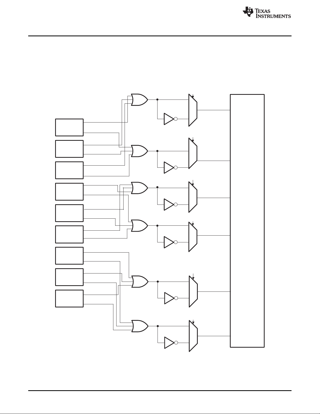
0
1
EXTSOCAG1
POLSEL
PulseStretcher
,
32HSPCLKCyclesW
ideandThentoChipPins
EXTSOCAG1
ePWM2
ePWM2SOCA
ePWM2SOCB
ePWM1
ePWM1SOCA
ePWM1SOCB
ePWM3
ePWM3SOCA
ePWM3SOCB
ePWM4
ePWM4SOCA
ePWM4SOCB
0
1
EXTSOCAG4
POLSEL
EXTSOCAG4
ePWM6
ePWM6SOCA
ePWM6SOCB
ePWM5
ePWM5SOCA
ePWM5SOCB
ePWM7
ePWM7SOCA
ePWM7SOCB
ePWM8
ePWM8SOCA
ePWM4SOCB
0
1
EXTSOCBG1
POLSEL
EXTSOCSBG1
0
1
EXTSOCBG4
POLSEL
EXTSOCBG4
ePWM9
ePWM9SOCA
ePWM9SOCB
0
1
EXTSOCAG7
POLSEL
EXTSOCAG7
0
1
EXTSOCBG7
POLSEL
EXTSOCBG7
ePWM Submodules
Each ePWM module has one interrupt request line connected to the PIE and two start of conversion
signals (one for each sequencer) connected to the ADC module. As shown in Figure 42, ADC start of
conversion for all ePWM modules are ORed together and hence multiple modules can initiate an ADC
start of conversion. If two requests occur on one start of conversion line, then only one will be recognized
by the ADC.
Figure 42. Event-Trigger Submodule Inter-Connectivity of ADC Start of Conversion
www.ti.com
The event-trigger submodule monitors various event conditions (the left side inputs to event-trigger
submodule shown in Figure 43) and can be configured to prescale these events before issuing an
Interrupt request or an ADC start of conversion. The event-trigger prescaling logic can issue Interrupt
requests and ADC start of conversion at:
• Every event
64
TMS320x2833x, 2823x Enhanced Pulse Width Modulator (ePWM) Module SPRUG04A–October 2008–Revised July 2009
© 2008–2009, Texas Instruments Incorporated
Submit Documentation Feedback
Page 65

PIE
Event Trigger
Module Logic
CTR=Zero
CTR=PRD
CTR=CMPA
EPWMxINTn
CTR_dir
Direction
qualifier
CTRU=CMPA
ETSEL reg
EPWMxSOCA
/n
/n
/n
EPWMxSOCB
ADC
clear
count
count
clear
count
clear
CTRD=CMPA
CTRU=CMPB
CTRD=CMPB
ETPS reg
ETFLG reg
ETCLR reg
ETFRC reg
www.ti.com
• Every second event
• Every third event
The key registers used to configure the event-trigger submodule are shown in Table 20:
ePWM Submodules
Figure 43. Event-Trigger Submodule Showing Event Inputs and Prescaled Outputs
Table 20. Event-Trigger Submodule Registers
Register Name Address offset Shadowed Description
ETSEL 0x0019 No Event-trigger Selection Register
ETPS 0x001A No Event-trigger Prescale Register
ETFLG 0x001B No Event-trigger Flag Register
ETCLR 0x001C No Event-trigger Clear Register
ETFRC 0x001D No Event-trigger Force Register
• ETSEL—This selects which of the possible events will trigger an interrupt or start an ADC conversion
• ETPS—This programs the event prescaling options mentioned above.
• ETFLG—These are flag bits indicating status of the selected and prescaled events.
• ETCLR—These bits allow you to clear the flag bits in the ETFLG register via software.
• ETFRC—These bits allow software forcing of an event. Useful for debugging or s/w intervention.
A more detailed look at how the various register bits interact with the Interrupt and ADC start of
conversion logic are shown in Figure 44, Figure 45, and Figure 46.
Figure 44 shows the event-trigger's interrupt generation logic. The interrupt-period (ETPS[INTPRD]) bits
specify the number of events required to cause an interrupt pulse to be generated. The choices available
are:
• Do not generate an interrupt.
• Generate an interrupt on every event
• Generate an interrupt on every second event
• Generate an interrupt on every third event
Which event can cause an interrupt is configured by the interrupt selection (ETSEL[INTSEL]) bits. The
event can be one of the following:
• Time-base counter equal to zero (TBCTR = 0x0000).
• Time-base counter equal to period (TBCTR = TBPRD).
• Time-base counter equal to the compare A register (CMPA) when the timer is incrementing.
• Time-base counter equal to the compare A register (CMPA) when the timer is decrementing.
SPRUG04A–October 2008–Revised July 2009 TMS320x2833x, 2823x Enhanced Pulse Width Modulator (ePWM) Module
Submit Documentation Feedback
© 2008–2009, Texas Instruments Incorporated
65
Page 66
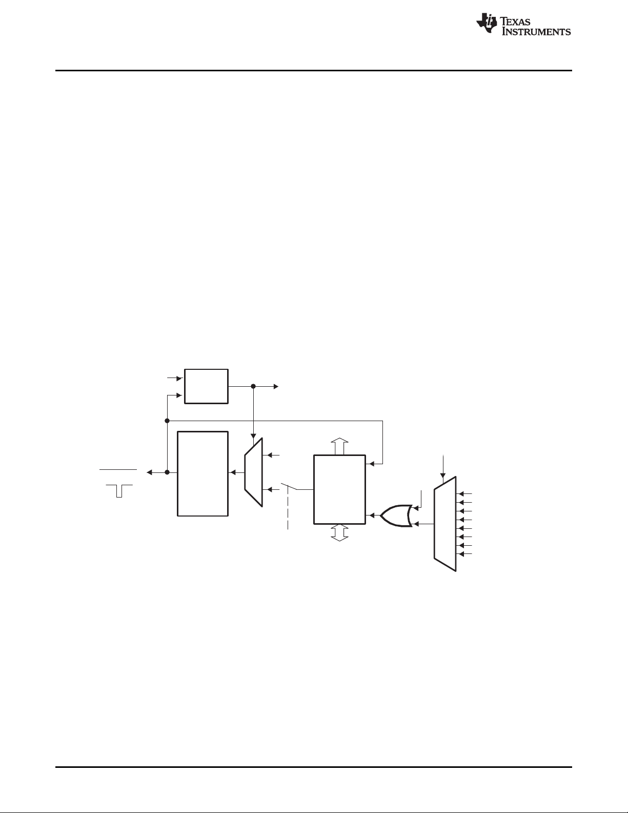
Latch
Generate
interrupt
pulse
when
input = 1
2-bit
Counter
Set
Clear
1
0
0
Clear CNT
Inc CNT
ETPS[INTCNT]
ETPS[INTPRD]
ETCLR[INT]
EPWMxINT
ETFRC[INT]
ETSEL[INT]
ETFLG[INT]
ETSEL[INTSEL]
000
001
010
011
100
101
111
101
0
0
CTRU=CMPA
CTRD=CMPA
CTRU=CMPB
CTRD=CMPB
CTR=Zero
CTR=PRD
ePWM Submodules
• Time-base counter equal to the compare B register (CMPB) when the timer is incrementing.
• Time-base counter equal to the compare B register (CMPB) when the timer is decrementing.
The number of events that have occurred can be read from the interrupt event counter (ETPS[INTCNT])
register bits. That is, when the specified event occurs the ETPS[INTCNT] bits are incremented until they
reach the value specified by ETPS[INTPRD]. When ETPS[INTCNT] = ETPS[INTPRD] the counter stops
counting and its output is set. The counter is only cleared when an interrupt is sent to the PIE.
When ETPS[INTCNT] reaches ETPS[INTPRD] the following behaviors will occur:
• If interrupts are enabled, ETSEL[INTEN] = 1 and the interrupt flag is clear, ETFLG[INT] = 0, then an
interrupt pulse is generated and the interrupt flag is set, ETFLG[INT] = 1, and the event counter is
cleared ETPS[INTCNT] = 0. The counter will begin counting events again.
• If interrupts are disabled, ETSEL[INTEN] = 0, or the interrupt flag is set, ETFLG[INT] = 1, the counter
stops counting events when it reaches the period value ETPS[INTCNT] = ETPS[INTPRD].
• If interrupts are enabled, but the interrupt flag is already set, then the counter will hold its output high
until the ENTFLG[INT] flag is cleared. This allows for one interrupt to be pending while one is serviced.
Writing to the INTPRD bits will automatically clear the counter INTCNT = 0 and the counter output will be
reset (so no interrupts are generated). Writing a 1 to the ETFRC[INT] bit will increment the event counter
INTCNT. The counter will behave as described above when INTCNT = INTPRD. When INTPRD = 0, the
counter is disabled and hence no events will be detected and the ETFRC[INT] bit is also ignored.
The above definition means that you can generate an interrupt on every event, on every second event, or
on every third event. An interrupt cannot be generated on every fourth or more events.
www.ti.com
Figure 44. Event-Trigger Interrupt Generator
66
Figure 45 shows the operation of the event-trigger's start-of-conversion-A (SOCA) pulse generator. The
ETPS[SOCACNT] counter and ETPS[SOCAPRD] period values behave similarly to the interrupt generator
except that the pulses are continuously generated. That is, the pulse flag ETFLG[SOCA] is latched when a
pulse is generated, but it does not stop further pulse generation. The enable/disable bit ETSEL[SOCAEN]
stops pulse generation, but input events can still be counted until the period value is reached as with the
interrupt generation logic. The event that will trigger an SOCA and SOCB pulse can be configured
separately in the ETSEL[SOCASEL] and ETSEL[SOCBSEL] bits. The possible events are the same
events that can be specified for the interrupt generation logic .
TMS320x2833x, 2823x Enhanced Pulse Width Modulator (ePWM) Module SPRUG04A–October 2008–Revised July 2009
© 2008–2009, Texas Instruments Incorporated
Submit Documentation Feedback
Page 67
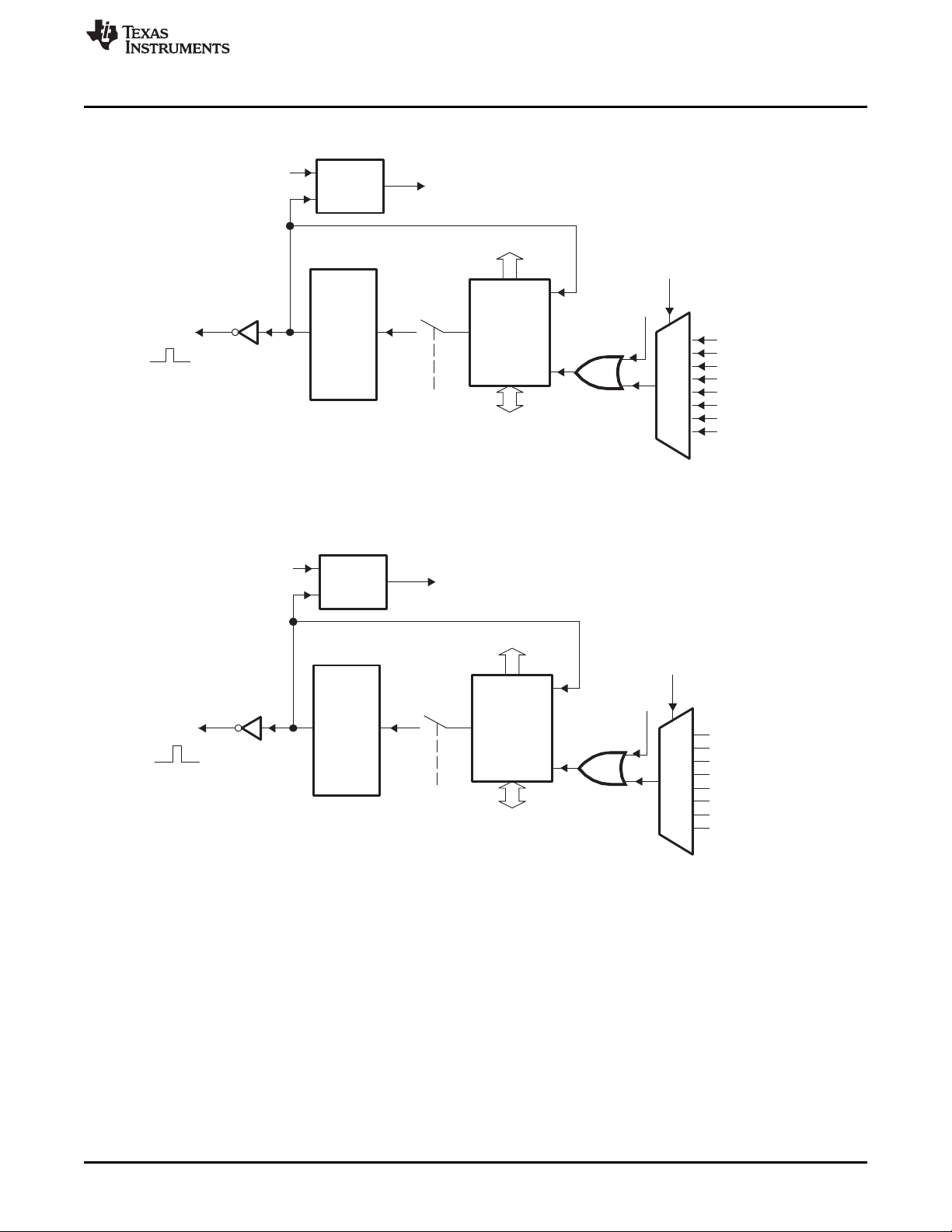
Latch
Generate
SOC
pulse
when
input=1
2-bit
Counter
Set
Clear
ClearCNT
IncCNT
ETPS[SOCACNT]
ETPS[SOCAPRD]
ETCLR[SOCA]
SOCA
ETFRC[SOCA]
ETSEL[SOCAEN]
ETFLG[SOCA]
ETSEL[SOCASEL]
000
001
010
011
100
101
111
101
0
0
CTRU=CMPA
CTRD=CMPA
CTRU=CMPB
CTRD=CMPB
CTR=Zero
CTR=PRD
Latch
Generate
SOC
pulse
when
input=1
2-bit
Counter
Set
Clear
ClearCNT
IncCNT
ETPS[SOCBCNT]
ETPS[SOCBPRD]
ETCLR[SOCB]
SOCB
ETFRC[SOCB]
ETSEL[SOCBEN]
ETFLG[SOCB]
ETSEL[SOCBSEL]
000
001
010
011
100
101
111
101
0
0
CTRU=CMPA
CTRD=CMPA
CTRU=CMPB
CTRD=CMPB
CTR=Zero
CTR=PRD
www.ti.com
Figure 46 shows the operation of the event-trigger's start-of-conversion-B (SOCB) pulse generator. The
event-trigger's SOCB pulse generator operates the same way as the SOCA.
ePWM Submodules
Figure 45. Event-Trigger SOCA Pulse Generator
Figure 46. Event-Trigger SOCB Pulse Generator
SPRUG04A–October 2008–Revised July 2009 TMS320x2833x, 2823x Enhanced Pulse Width Modulator (ePWM) Module
Submit Documentation Feedback
© 2008–2009, Texas Instruments Incorporated
67
Page 68
CTR = 0
CTR=CMPB
X
EN
SyncOut
Phase reg
EPWMxA
EPWMxB
SyncIn
Φ=0°
Applications to Power Topologies
3 Applications to Power Topologies
An ePWM module has all the local resources necessary to operate completely as a standalone module or
to operate in synchronization with other identical ePWM modules.
3.1 Overview of Multiple Modules
Previously in this user's guide, all discussions have described the operation of a single module. To
facilitate the understanding of multiple modules working together in a system, the ePWM module
described in reference is represented by the more simplified block diagram shown in Figure 47. This
simplified ePWM block shows only the key resources needed to explain how a multiswitch power topology
is controlled with multiple ePWM modules working together.
Figure 47. Simplified ePWM Module
www.ti.com
3.2 Key Configuration Capabilities
The key configuration choices available to each module are as follows:
• Options for SyncIn
– Load own counter with phase register on an incoming sync strobe—enable (EN) switch closed
– Do nothing or ignore incoming sync strobe—enable switch open
– Sync flow-through - SyncOut connected to SyncIn
– Master mode, provides a sync at PWM boundaries—SyncOut connected to CTR = PRD
– Master mode, provides a sync at any programmable point in time—SyncOut connected to CTR =
CMPB
– Module is in standalone mode and provides No sync to other modules—SyncOut connected to X
(disabled)
• Options for SyncOut
– Sync flow-through - SyncOut connected to SyncIn
– Master mode, provides a sync at PWM boundaries—SyncOut connected to CTR = PRD
– Master mode, provides a sync at any programmable point in time—SyncOut connected to CTR =
CMPB
– Module is in standalone mode and provides No sync to other modules—SyncOut connected to X
(disabled)
For each choice of SyncOut, a module may also choose to load its own counter with a new phase value
on a SyncIn strobe input or choose to ignore it, i.e., via the enable switch. Although various combinations
are possible, the two most common—master module and slave module modes—are shown in Figure 48.
68
TMS320x2833x, 2823x Enhanced Pulse Width Modulator (ePWM) Module SPRUG04A–October 2008–Revised July 2009
© 2008–2009, Texas Instruments Incorporated
Submit Documentation Feedback
Page 69
CTR=0
CTR=CMPB
X
EN
SyncOut
Phase reg
Ext SyncIn
(optional)
EPWM1A
EPWM1B
SyncOut
Phase reg
CTR=CMPB
CTR=0
X
EN
EPWM2B
EPWM2A
Slave
Master
SyncIn
SyncIn
1
2
Φ=0°
Φ=0°
www.ti.com
Applications to Power Topologies
Figure 48. EPWM1 Configured as a Typical Master, EPWM2 Configured as a Slave
3.3 Controlling Multiple Buck Converters With Independent Frequencies
One of the simplest power converter topologies is the buck. A single ePWM module configured as a
master can control two buck stages with the same PWM frequency. If independent frequency control is
required for each buck converter, then one ePWM module must be allocated for each converter stage.
Figure 49 shows four buck stages, each running at independent frequencies. In this case, all four ePWM
modules are configured as Masters and no synchronization is used. Figure 50 shows the waveforms
generated by the setup shown in Figure 49; note that only three waveforms are shown, although there are
four stages.
SPRUG04A–October 2008–Revised July 2009 TMS320x2833x, 2823x Enhanced Pulse Width Modulator (ePWM) Module
Submit Documentation Feedback
© 2008–2009, Texas Instruments Incorporated
69
Page 70
CTR=zero
CTR=CMPB
X
En
SyncOut
Phase reg
Ext SyncIn
(optional)
EPWM1A
EPWM1B
SyncOut
Phase reg
CTR=CMPB
CTR=zero
X
En
EPWM2B
EPWM2A
Master2
Master1
SyncIn
CTR=zero
CTR=CMPB
SyncOut
X
EPWM3B
Phase reg
Master3
En
EPWM3A
1
2
3
Φ=X
Φ=X
Φ=X
CTR=zero
CTR=CMPB
SyncOut
X
EPWM4B
Phase reg
Master4
En
EPWM4A
3
Φ=X
Buck #1
Vout1Vin1
EPWM1A
Buck #2
Vin2
EPWM2A
Vout2
Buck #4
Buck #3
Vin3
EPWM4A
Vin4
EPWM3A
Vout3
Vout4
SyncIn
SyncIn
SyncIn
Applications to Power Topologies
www.ti.com
Figure 49. Control of Four Buck Stages. Here F
PWM1
≠ F
PWM2
≠ F
PWM3
≠ F
PWM4
NOTE: Θ = X indicates value in phase register is a "don't care"
70
TMS320x2833x, 2823x Enhanced Pulse Width Modulator (ePWM) Module SPRUG04A–October 2008–Revised July 2009
© 2008–2009, Texas Instruments Incorporated
Submit Documentation Feedback
Page 71
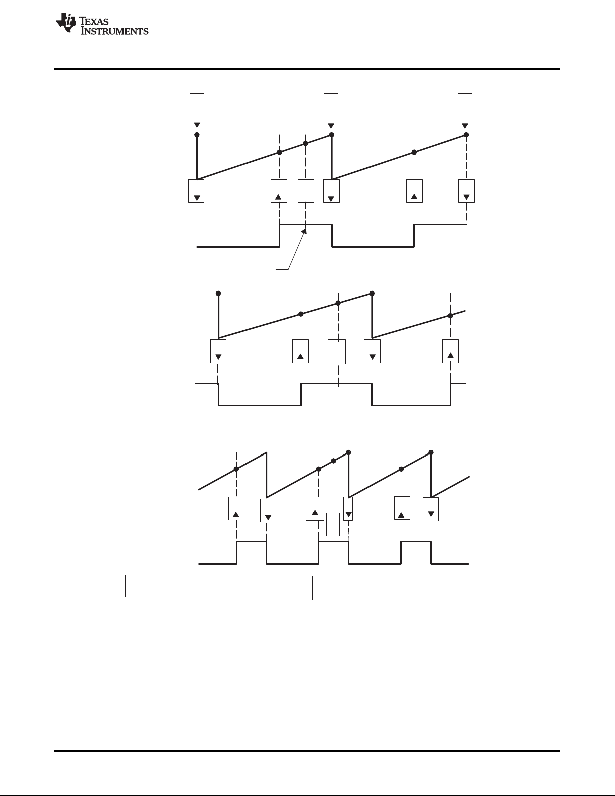
P CA CBAP CA P
Pulse center
EPWM1A
700 950
1200
P CA CB
A
P CA
700 1150
1400
EPWM2A
CA P
CA
CB
A
P CA P
500
650
800
EPWM3A
P
Indicates this event triggers an interrupt CB
A
I
P
I
P
I
P
I
Indicates this event triggers an ADC start
of conversion
www.ti.com
Applications to Power Topologies
Figure 50. Buck Waveforms for Figure 49 (Note: Only three bucks shown here)
SPRUG04A–October 2008–Revised July 2009 TMS320x2833x, 2823x Enhanced Pulse Width Modulator (ePWM) Module
Submit Documentation Feedback
© 2008–2009, Texas Instruments Incorporated
71
Page 72

Applications to Power Topologies
Example 9. Configuration for Example in Figure 50
//=====================================================================
// (Note: code for only 3 modules shown)
// Initialization Time
//========================
// EPWM Module 1 config
EPwm1Regs.TBPRD = 1200; // Period = 1201 TBCLK counts
EPwm1Regs.TBPHS.half.TBPHS = 0; // Set Phase register to zero
EPwm1Regs.TBCTL.bit.CTRMODE = TB_COUNT_UP; // Asymmetrical mode
EPwm1Regs.TBCTL.bit.PHSEN = TB_DISABLE; // Phase loading disabled
EPwm1Regs.TBCTL.bit.PRDLD = TB_SHADOW;
EPwm1Regs.TBCTL.bit.SYNCOSEL = TB_SYNC_DISABLE;
EPwm1Regs.CMPCTL.bit.SHDWAMODE = CC_SHADOW;
EPwm1Regs.CMPCTL.bit.SHDWBMODE = CC_SHADOW;
EPwm1Regs.CMPCTL.bit.LOADAMODE = CC_CTR_ZERO; // load on CTR=Zero
EPwm1Regs.CMPCTL.bit.LOADBMODE = CC_CTR_ZERO; // load on CTR=Zero
EPwm1Regs.AQCTLA.bit.PRD = AQ_CLEAR;
EPwm1Regs.AQCTLA.bit.CAU = AQ_SET;
// EPWM Module 2 config
EPwm2Regs.TBPRD = 1400; // Period = 1401 TBCLK counts
EPwm2Regs.TBPHS.half.TBPHS = 0; // Set Phase register to zero
EPwm2Regs.TBCTL.bit.CTRMODE = TB_COUNT_UP; // Asymmetrical mode
EPwm2Regs.TBCTL.bit.PHSEN = TB_DISABLE; // Phase loading disabled
EPwm2Regs.TBCTL.bit.PRDLD = TB_SHADOW;
EPwm2Regs.TBCTL.bit.SYNCOSEL = TB_SYNC_DISABLE;
EPwm2Regs.CMPCTL.bit.SHDWAMODE = CC_SHADOW;
EPwm2Regs.CMPCTL.bit.SHDWBMODE = CC_SHADOW;
EPwm2Regs.CMPCTL.bit.LOADAMODE = CC_CTR_ZERO; // load on CTR=Zero
EPwm2Regs.CMPCTL.bit.LOADBMODE = CC_CTR_ZERO; // load on CTR=Zero
EPwm2Regs.AQCTLA.bit.PRD = AQ_CLEAR;
EPwm2Regs.AQCTLA.bit.CAU = AQ_SET;
// EPWM Module 3 config
EPwm3Regs.TBPRD = 800; // Period = 801 TBCLK counts
EPwm3Regs.TBPHS.half.TBPHS = 0; // Set Phase register to zero
EPwm3Regs.TBCTL.bit.CTRMODE = TB_COUNT_UP;
EPwm3Regs.TBCTL.bit.PHSEN = TB_DISABLE; // Phase loading disabled
EPwm3Regs.TBCTL.bit.PRDLD = TB_SHADOW;
EPwm3Regs.TBCTL.bit.SYNCOSEL = TB_SYNC_DISABLE;
EPwm3Regs.CMPCTL.bit.SHDWAMODE = CC_SHADOW;
EPwm3Regs.CMPCTL.bit.SHDWBMODE = CC_SHADOW;
EPwm3Regs.CMPCTL.bit.LOADAMODE = CC_CTR_ZERO; // load on CTR=Zero
EPwm3Regs.CMPCTL.bit.LOADBMODE = CC_CTR_ZERO; // load on CTR=Zero
EPwm3Regs.AQCTLA.bit.PRD = AQ_CLEAR;
EPwm3Regs.AQCTLA.bit.CAU = AQ_SET;
//
// Run Time (Note: Example execution of one run-time instant)
//=========================================================
EPwm1Regs.CMPA.half.CMPA = 700; // adjust duty for output EPWM1A
EPwm2Regs.CMPA.half.CMPA = 700; // adjust duty for output EPWM2A
EPwm3Regs.CMPA.half.CMPA = 500; // adjust duty for output EPWM3A
www.ti.com
72
TMS320x2833x, 2823x Enhanced Pulse Width Modulator (ePWM) Module SPRUG04A–October 2008–Revised July 2009
Submit Documentation Feedback
© 2008–2009, Texas Instruments Incorporated
Page 73

CTR=zero
CTR=CMPB
X
En
Φ=0°
SyncOut
Phase reg
Ext SyncIn
(optional)
EPWM1A
EPWM1B
SyncOut
Phase reg
CTR=CMPB
CTR=zero
X
Φ=X
En
EPWM2B
EPWM2A
Slave
Master
Buck #1
Vout1Vin1
EPWM1A
Buck #2
Vin2
EPWM1B
Vout2
Buck #4
Buck #3
Vin3
EPWM2B
Vin4
EPWM2A
Vout3
Vout4
SyncIn
SyncIn
www.ti.com
3.4 Controlling Multiple Buck Converters With Same Frequencies
If synchronization is a requirement, ePWM module 2 can be configured as a slave and can operate at
integer multiple (N) frequencies of module 1. The sync signal from master to slave ensures these modules
remain locked. Figure 51 shows such a configuration; Figure 52 shows the waveforms generated by the
configuration.
Applications to Power Topologies
Figure 51. Control of Four Buck Stages. (Note: F
PWM2
= N x F
PWM1
)
SPRUG04A–October 2008–Revised July 2009 TMS320x2833x, 2823x Enhanced Pulse Width Modulator (ePWM) Module
Submit Documentation Feedback
© 2008–2009, Texas Instruments Incorporated
73
Page 74

200
400
600
400
200
300
500
300
500
Z
I
A
P
CA
CA
Z
I
Z
I
A
P
CA
CA
CB
CB
CB
CB
CA CA
CA CA
CB
CB
CB
CB
Applications to Power Topologies
www.ti.com
Figure 52. Buck Waveforms for Figure 51 (Note: F
PWM2
= F
PWM1)
)
74
TMS320x2833x, 2823x Enhanced Pulse Width Modulator (ePWM) Module SPRUG04A–October 2008–Revised July 2009
© 2008–2009, Texas Instruments Incorporated
Submit Documentation Feedback
Page 75

www.ti.com
Example 10. Code Snippet for Configuration in Figure 51
//========================
// EPWM Module 1 config
EPwm1Regs.TBPRD = 600; // Period = 1200 TBCLK counts
EPwm1Regs.TBPHS.half.TBPHS = 0; // Set Phase register to zero
EPwm1Regs.TBCTL.bit.CTRMODE = TB_COUNT_UPDOWN; // Symmetrical mode
EPwm1Regs.TBCTL.bit.PHSEN = TB_DISABLE; // Master module
EPwm1Regs.TBCTL.bit.PRDLD = TB_SHADOW;
EPwm1Regs.TBCTL.bit.SYNCOSEL = TB_CTR_ZERO; // Sync down-stream module
EPwm1Regs.CMPCTL.bit.SHDWAMODE = CC_SHADOW;
EPwm1Regs.CMPCTL.bit.SHDWBMODE = CC_SHADOW;
EPwm1Regs.CMPCTL.bit.LOADAMODE = CC_CTR_ZERO; // load on CTR=Zero
EPwm1Regs.CMPCTL.bit.LOADBMODE = CC_CTR_ZERO; // load on CTR=Zero
EPwm1Regs.AQCTLA.bit.CAU = AQ_SET; // set actions for EPWM1A
EPwm1Regs.AQCTLA.bit.CAD = AQ_CLEAR;
EPwm1Regs.AQCTLB.bit.CBU = AQ_SET; // set actions for EPWM1B
EPwm1Regs.AQCTLB.bit.CBD = AQ_CLEAR;
// EPWM Module 2 config
EPwm2Regs.TBPRD = 600; // Period = 1200 TBCLK counts
EPwm2Regs.TBPHS.half.TBPHS = 0; // Set Phase register to zero
EPwm2Regs.TBCTL.bit.CTRMODE = TB_COUNT_UPDOWN; // Symmetrical mode
EPwm2Regs.TBCTL.bit.PHSEN = TB_ENABLE; // Slave module
EPwm2Regs.TBCTL.bit.PRDLD = TB_SHADOW;
EPwm2Regs.TBCTL.bit.SYNCOSEL = TB_SYNC_IN; // sync flow-through
EPwm2Regs.CMPCTL.bit.SHDWAMODE = CC_SHADOW;
EPwm2Regs.CMPCTL.bit.SHDWBMODE = CC_SHADOW;
EPwm2Regs.CMPCTL.bit.LOADAMODE = CC_CTR_ZERO; // load on CTR=Zero
EPwm2Regs.CMPCTL.bit.LOADBMODE = CC_CTR_ZERO; // load on CTR=Zero
EPwm2Regs.AQCTLA.bit.CAU = AQ_SET; // set actions for EPWM2A
EPwm2Regs.AQCTLA.bit.CAD = AQ_CLEAR;
EPwm2Regs.AQCTLB.bit.CBU = AQ_SET; // set actions for EPWM2B
EPwm2Regs.AQCTLB.bit.CBD = AQ_CLEAR;
//
// Run Time (Note: Example execution of one run-time instance)
//===========================================================
EPwm1Regs.CMPA.half.CMPA = 400; // adjust duty for output EPWM1A
EPwm1Regs.CMPB = 200; // adjust duty for output EPWM1B
EPwm2Regs.CMPA.half.CMPA = 500; // adjust duty for output EPWM2A
EPwm2Regs.CMPB = 300; // adjust duty for output EPWM2B
Applications to Power Topologies
SPRUG04A–October 2008–Revised July 2009 TMS320x2833x, 2823x Enhanced Pulse Width Modulator (ePWM) Module
Submit Documentation Feedback
© 2008–2009, Texas Instruments Incorporated
75
Page 76

CTR=zero
CTR=CMPB
X
En
SyncOut
Phase reg
Ext SyncIn
(optional)
EPWM1A
EPWM1B
SyncOut
Phase reg
CTR=CMPB
CTR=zero
X
En
EPWM2B
EPWM2A
Slave
Master
V
out1
EPWM1A
SyncIn
SyncIn
V
DC_bus
EPWM1B
EPWM2B
EPWM2A
V
DC_bus
V
out2
Φ=0°
Φ=0°
Applications to Power Topologies
3.5 Controlling Multiple Half H-Bridge (HHB) Converters
Topologies that require control of multiple switching elements can also be addressed with these same
ePWM modules. It is possible to control a Half-H bridge stage with a single ePWM module. This control
can be extended to multiple stages. Figure 53 shows control of two synchronized Half-H bridge stages
where stage 2 can operate at integer multiple (N) frequencies of stage 1. Figure 54 shows the waveforms
generated by the configuration shown in Figure 53.
Module 2 (slave) is configured for Sync flow-through; if required, this configuration allows for a third Half-H
bridge to be controlled by PWM module 3 and also, most importantly, to remain in synchronization with
master module 1.
www.ti.com
Figure 53. Control of Two Half-H Bridge Stages (F
PWM2
= N x F
PWM1
)
76
TMS320x2833x, 2823x Enhanced Pulse Width Modulator (ePWM) Module SPRUG04A–October 2008–Revised July 2009
© 2008–2009, Texas Instruments Incorporated
Submit Documentation Feedback
Page 77

600
200
400
400
200
250
500
500
250
Pulse Center
A
CB
CA
Z
ZIZ
I
Z
I
Z
I
A
CB
CA
Z
Z
A
CB
CA
Pulse Center
Z
A
CB
CA
A
CB
CA
Z
A
CB
CA
Z
A
CB
Z
CA
A
CB
Z
CA
www.ti.com
Applications to Power Topologies
Figure 54. Half-H Bridge Waveforms for Figure 53 (Note: Here F
PWM2
= F
PWM1
)
SPRUG04A–October 2008–Revised July 2009 TMS320x2833x, 2823x Enhanced Pulse Width Modulator (ePWM) Module
Submit Documentation Feedback
© 2008–2009, Texas Instruments Incorporated
77
Page 78

Applications to Power Topologies
Example 11. Code Snippet for Configuration in Figure 53
//=====================================================================
// Config
//=====================================================================
// Initialization Time
//========================
// EPWM Module 1 config
EPwm1Regs.TBPRD = 600; // Period = 1200 TBCLK counts
EPwm1Regs.TBPHS.half.TBPHS = 0; // Set Phase register to zero
EPwm1Regs.TBCTL.bit.CTRMODE = TB_COUNT_UPDOWN; // Symmetrical mode
EPwm1Regs.TBCTL.bit.PHSEN = TB_DISABLE; // Master module
EPwm1Regs.TBCTL.bit.PRDLD = TB_SHADOW;
EPwm1Regs.TBCTL.bit.SYNCOSEL = TB_CTR_ZERO; // Sync down-stream module
EPwm1Regs.CMPCTL.bit.SHDWAMODE = CC_SHADOW;
EPwm1Regs.CMPCTL.bit.SHDWBMODE = CC_SHADOW;
EPwm1Regs.CMPCTL.bit.LOADAMODE = CC_CTR_ZERO; // load on CTR=Zero
EPwm1Regs.CMPCTL.bit.LOADBMODE = CC_CTR_ZERO; // load on CTR=Zero
EPwm1Regs.AQCTLA.bit.ZRO = AQ_SET; // set actions for EPWM1A
EPwm1Regs.AQCTLA.bit.CAU = AQ_CLEAR;
EPwm1Regs.AQCTLB.bit.ZRO = AQ_CLEAR; // set actions for EPWM1B
EPwm1Regs.AQCTLB.bit.CAD = AQ_SET;
// EPWM Module 2 config
EPwm2Regs.TBPRD = 600; // Period = 1200 TBCLK counts
EPwm2Regs.TBPHS.half.TBPHS = 0; // Set Phase register to zero
EPwm2Regs.TBCTL.bit.CTRMODE = TB_COUNT_UPDOWN; // Symmetrical mode
EPwm2Regs.TBCTL.bit.PHSEN = TB_ENABLE; // Slave module
EPwm2Regs.TBCTL.bit.PRDLD = TB_SHADOW;
EPwm2Regs.TBCTL.bit.SYNCOSEL = TB_SYNC_IN; // sync flow-through
EPwm2Regs.CMPCTL.bit.SHDWAMODE = CC_SHADOW;
EPwm2Regs.CMPCTL.bit.SHDWBMODE = CC_SHADOW;
EPwm2Regs.CMPCTL.bit.LOADAMODE = CC_CTR_ZERO; // load on CTR=Zero
EPwm2Regs.CMPCTL.bit.LOADBMODE = CC_CTR_ZERO; // load on CTR=Zero
EPwm2Regs.AQCTLA.bit.ZRO = AQ_SET; // set actions for EPWM1A
EPwm2Regs.AQCTLA.bit.CAU = AQ_CLEAR;
EPwm2Regs.AQCTLB.bit.ZRO = AQ_CLEAR; // set actions for EPWM1B
EPwm2Regs.AQCTLB.bit.CAD = AQ_SET;
//============================================================
EPwm1Regs.CMPA.half.CMPA = 400; // adjust duty for output EPWM1A & EPWM1B
www.ti.com
EPwm1Regs.CMPB = 200; // adjust point-in-time for ADCSOC trigger
EPwm2Regs.CMPA.half.CMPA = 500; // adjust duty for output EPWM2A & EPWM2B
EPwm2Regs.CMPB = 250; // adjust point-in-time for ADCSOC trigger
3.6 Controlling Dual 3-Phase Inverters for Motors (ACI and PMSM)
The idea of multiple modules controlling a single power stage can be extended to the 3-phase Inverter
case. In such a case, six switching elements can be controlled using three PWM modules, one for each
leg of the inverter. Each leg must switch at the same frequency and all legs must be synchronized. A
master + two slaves configuration can easily address this requirement. Figure 55 shows how six PWM
modules can control two independent 3-phase Inverters; each running a motor.
As in the cases shown in the previous sections, we have a choice of running each inverter at a different
frequency (module 1 and module 4 are masters as in Figure 55), or both inverters can be synchronized by
using one master (module 1) and five slaves. In this case, the frequency of modules 4, 5, and 6 (all equal)
can be integer multiples of the frequency for modules 1, 2, 3 (also all equal).
78
TMS320x2833x, 2823x Enhanced Pulse Width Modulator (ePWM) Module SPRUG04A–October 2008–Revised July 2009
Submit Documentation Feedback
© 2008–2009, Texas Instruments Incorporated
Page 79

Φ=0°
CTR=zero
CTR=CMPB
X
En
SyncOut
Phase reg
Ext SyncIn
(optional)
EPWM1A
EPWM1B
SyncOut
Phase reg
CTR=CMPB
CTR=zero
X
En
EPWM2B
EPWM2A
Slave
Master
EPWM1A
EPWM1B
EPWM2A
EPWM2B EPWM3B
EPWM3A
VAB
VCD
VEF
3 phase motor
EPWM4B EPWM5B
VAB
EPWM4A
VCD
EPWM5A
EPWM6B
3 phase motor
VEF
EPWM6A
3 phase inverter #1
3 phase inverter #2
1
2
CTR=zero
CTR=CMPB
Phase reg
3
Slave
SyncOut
X
En
EPWM3B
EPWM3A
Phase reg
CTR=CMPB
CTR=zero
4
Slave
SyncOut
X
EPWM4A
EPWM4B
En
SyncOut
CTR=zero
CTR=CMPB
Phase reg
Phase reg
CTR=CMPB
CTR=zero
Slave
6
5
Slave
X
En
SyncIn
EPWM6B
EPWM6A
SyncOut
X
EPWM5A
EPWM5B
En
Φ=0°
Φ=0°
Φ=0°
Φ=0°
Φ=0°
SyncIn
SyncIn
SyncIn
SyncIn
SyncIn
www.ti.com
Applications to Power Topologies
Figure 55. Control of Dual 3-Phase Inverter Stages as Is Commonly Used in Motor Control
SPRUG04A–October 2008–Revised July 2009 TMS320x2833x, 2823x Enhanced Pulse Width Modulator (ePWM) Module
Submit Documentation Feedback
© 2008–2009, Texas Instruments Incorporated
79
Page 80
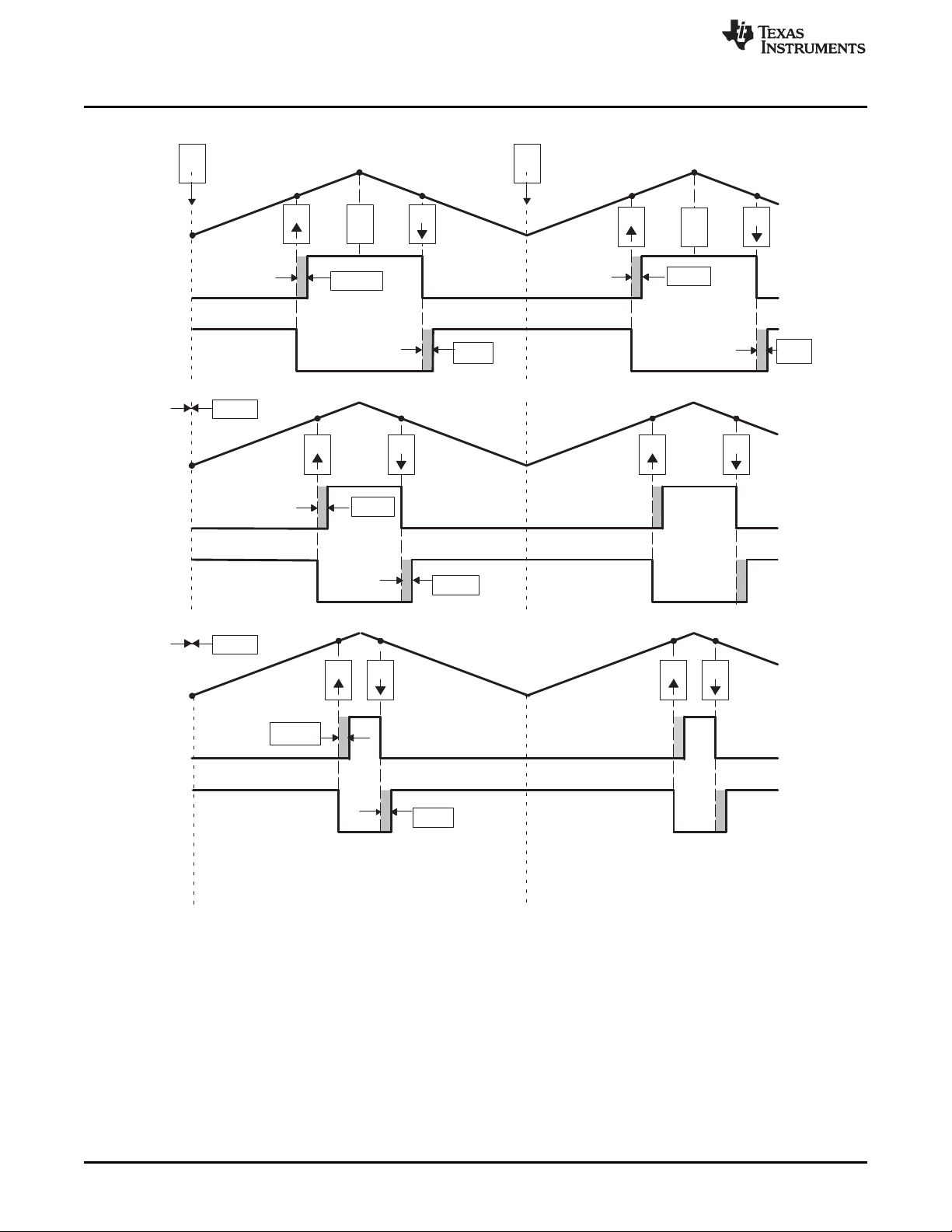
RED
FED
FED
FED
RED
RED
RED
FED
EPWM1A
Φ2=0
Φ3=0
800
500
500
600 600
700
700
Z
I
A
P
CA
CA
Z
I
A
P
CA
CA
CA CA CA CA
CA CA CA CA
Applications to Power Topologies
Figure 56. 3-Phase Inverter Waveforms for Figure 55 (Only One Inverter Shown)
www.ti.com
80
TMS320x2833x, 2823x Enhanced Pulse Width Modulator (ePWM) Module SPRUG04A–October 2008–Revised July 2009
© 2008–2009, Texas Instruments Incorporated
Submit Documentation Feedback
Page 81

www.ti.com
Example 12. Code Snippet for Configuration in Figure 55
//=====================================================================
// Configuration
//=====================================================================
// Initialization Time
//========================// EPWM Module 1 config
EPwm1Regs.TBPRD = 800; // Period = 1600 TBCLK counts
EPwm1Regs.TBPHS.half.TBPHS = 0; // Set Phase register to zero
EPwm1Regs.TBCTL.bit.CTRMODE = TB_COUNT_UPDOWN; // Symmetrical mode
EPwm1Regs.TBCTL.bit.PHSEN = TB_DISABLE; // Master module
EPwm1Regs.TBCTL.bit.PRDLD = TB_SHADOW;
EPwm1Regs.TBCTL.bit.SYNCOSEL = TB_CTR_ZERO; // Sync down-stream module
EPwm1Regs.CMPCTL.bit.SHDWAMODE = CC_SHADOW;
EPwm1Regs.CMPCTL.bit.SHDWBMODE = CC_SHADOW;
EPwm1Regs.CMPCTL.bit.LOADAMODE = CC_CTR_ZERO; // load on CTR=Zero
EPwm1Regs.CMPCTL.bit.LOADBMODE = CC_CTR_ZERO; // load on CTR=Zero
EPwm1Regs.AQCTLA.bit.CAU = AQ_SET; // set actions for EPWM1A
EPwm1Regs.AQCTLA.bit.CAD = AQ_CLEAR;
EPwm1Regs.DBCTL.bit.OUT_MODE = DB_FULL_ENABLE; // enable Dead-band module
EPwm1Regs.DBCTL.bit.POLSEL = DB_ACTV_HIC; // Active Hi complementary
EPwm1Regs.DBFED = 50; // FED = 50 TBCLKs
EPwm1Regs.DBRED = 50; // RED = 50 TBCLKs
// EPWM Module 2 config
EPwm2Regs.TBPRD = 800; // Period = 1600 TBCLK counts
EPwm2Regs.TBPHS.half.TBPHS = 0; // Set Phase register to zero
EPwm2Regs.TBCTL.bit.CTRMODE = TB_COUNT_UPDOWN; // Symmetrical mode
EPwm2Regs.TBCTL.bit.PHSEN = TB_ENABLE; // Slave module
EPwm2Regs.TBCTL.bit.PRDLD = TB_SHADOW;
EPwm2Regs.TBCTL.bit.SYNCOSEL = TB_SYNC_IN; // sync flow-through
EPwm2Regs.CMPCTL.bit.SHDWAMODE = CC_SHADOW;
EPwm2Regs.CMPCTL.bit.SHDWBMODE = CC_SHADOW;
EPwm2Regs.CMPCTL.bit.LOADAMODE = CC_CTR_ZERO; // load on CTR=Zero
EPwm2Regs.CMPCTL.bit.LOADBMODE = CC_CTR_ZERO; // load on CTR=Zero
EPwm2Regs.AQCTLA.bit.CAU = AQ_SET; // set actions for EPWM2A
EPwm2Regs.AQCTLA.bit.CAD = AQ_CLEAR;
EPwm2Regs.DBCTL.bit.OUT_MODE = DB_FULL_ENABLE; // enable Dead-band module
EPwm2Regs.DBCTL.bit.POLSEL = DB_ACTV_HIC; // Active Hi complementary
EPwm2Regs.DBFED = 50; // FED = 50 TBCLKs
EPwm2Regs.DBRED = 50; // RED = 50 TBCLKs
// EPWM Module 3 config
EPwm3Regs.TBPRD = 800; // Period = 1600 TBCLK counts
EPwm3Regs.TBPHS.half.TBPHS = 0; // Set Phase register to zero
EPwm3Regs.TBCTL.bit.CTRMODE = TB_COUNT_UPDOWN; // Symmetrical mode
EPwm3Regs.TBCTL.bit.PHSEN = TB_ENABLE; // Slave module
EPwm3Regs.TBCTL.bit.PRDLD = TB_SHADOW;
EPwm3Regs.TBCTL.bit.SYNCOSEL = TB_SYNC_IN; // sync flow-through
EPwm3Regs.CMPCTL.bit.SHDWAMODE = CC_SHADOW;
EPwm3Regs.CMPCTL.bit.SHDWBMODE = CC_SHADOW;
EPwm3Regs.CMPCTL.bit.LOADAMODE = CC_CTR_ZERO; // load on CTR=Zero
EPwm3Regs.CMPCTL.bit.LOADBMODE = CC_CTR_ZERO; // load on CTR=Zero
EPwm3Regs.AQCTLA.bit.CAU = AQ_SET; // set actions for EPWM3A
EPwm3Regs.AQCTLA.bit.CAD = AQ_CLEAR;
EPwm3Regs.DBCTL.bit.OUT_MODE = DB_FULL_ENABLE; // enable Dead-band module
EPwm3Regs.DBCTL.bit.POLSEL = DB_ACTV_HIC; // Active Hi complementary
EPwm3Regs.DBFED = 50; // FED = 50 TBCLKs
EPwm3Regs.DBRED = 50; // RED = 50 TBCLKs
// Run Time (Note: Example execution of one run-time instant)
//=========================================================
EPwm1Regs.CMPA.half.CMPA = 500; // adjust duty for output EPWM1A
EPwm2Regs.CMPA.half.CMPA = 600; // adjust duty for output EPWM2A
EPwm3Regs.CMPA.half.CMPA = 700; // adjust duty for output EPWM3A
Applications to Power Topologies
SPRUG04A–October 2008–Revised July 2009 TMS320x2833x, 2823x Enhanced Pulse Width Modulator (ePWM) Module
Submit Documentation Feedback
© 2008–2009, Texas Instruments Incorporated
81
Page 82

CTR=zero
CTR=CMPB
X
En
SyncOut
Phase reg
Ext SyncIn
(optional)
EPWM1A
EPWM1B
SyncOut
Phase reg
CTR=CMPB
CTR=zero
X
En
EPWM2B
EPWM2A
Slave
Master
SyncIn
SyncIn
1
2
Φ=0°
Φ=120°
Applications to Power Topologies
3.7 Practical Applications Using Phase Control Between PWM Modules
So far, none of the examples have made use of the phase register (TBPHS). It has either been set to zero
or its value has been a don't care. However, by programming appropriate values into TBPHS, multiple
PWM modules can address another class of power topologies that rely on phase relationship between
legs (or stages) for correct operation. As described in the TB module section, a PWM module can be
configured to allow a SyncIn pulse to cause the TBPHS register to be loaded into the TBCTR register. To
illustrate this concept, Figure 57 shows a master and slave module with a phase relationship of 120°, i.e.,
the slave leads the master.
Figure 57. Configuring Two PWM Modules for Phase Control
www.ti.com
82
Figure 58 shows the associated timing waveforms for this configuration. Here, TBPRD = 600 for both
master and slave. For the slave, TBPHS = 200 (i.e., 200/600 X 360° = 120°). Whenever the master
generates a SyncIn pulse (CTR = PRD), the value of TBPHS = 200 is loaded into the slave TBCTR
register so the slave time-base is always leading the master's time-base by 120°.
TMS320x2833x, 2823x Enhanced Pulse Width Modulator (ePWM) Module SPRUG04A–October 2008–Revised July 2009
© 2008–2009, Texas Instruments Incorporated
Submit Documentation Feedback
Page 83
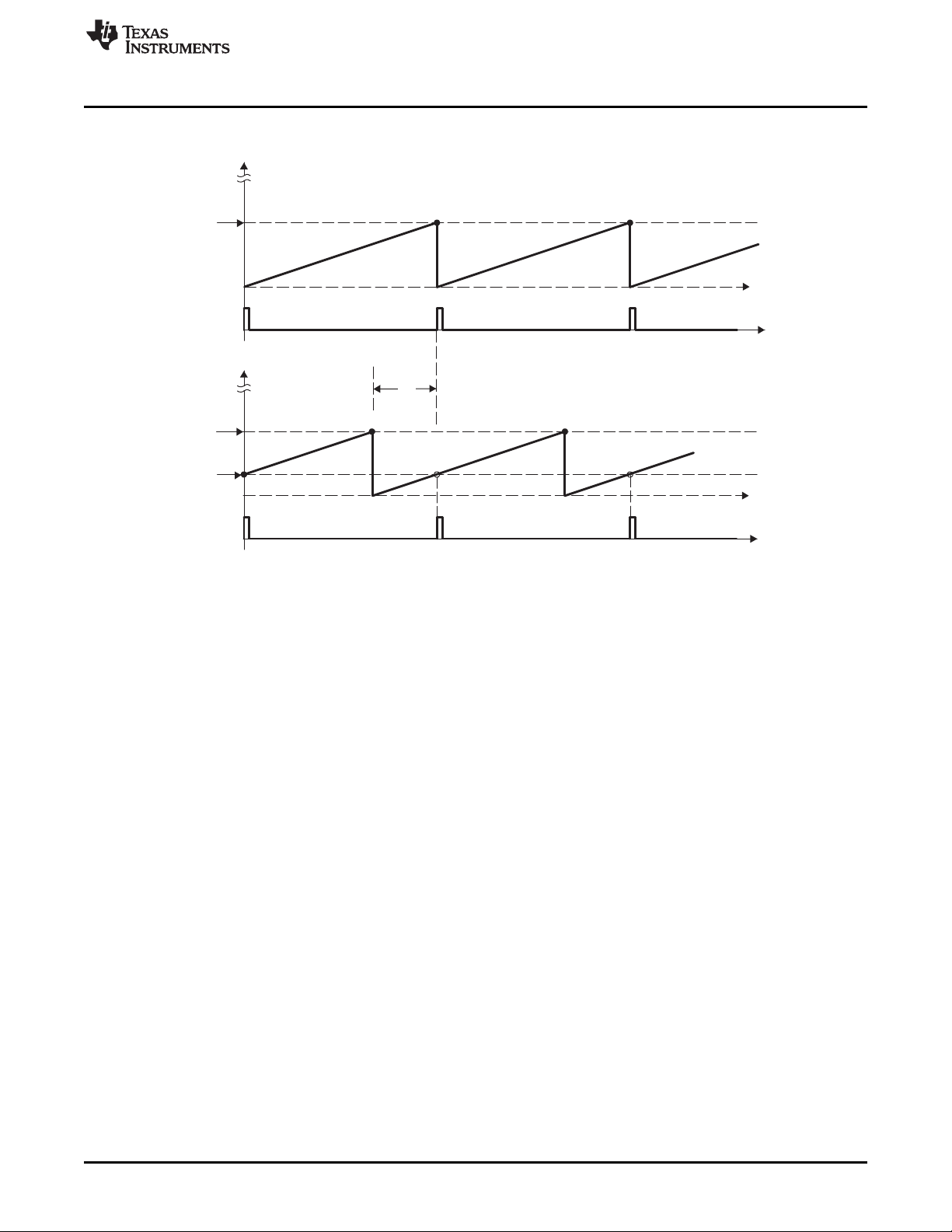
0000
FFFFh
TBPRD
TBCTR[0-15]
time
(SycnOut)
Master Module
Φ2
Phase = 120°
0000
FFFFh
TBPRD
TBCTR[0-15]
time
SyncIn
Slave Module
TBPHS
600 600
600 600
200
200
www.ti.com
Applications to Power Topologies
Figure 58. Timing Waveforms Associated With Phase Control Between 2 Modules
3.8 Controlling a 3-Phase Interleaved DC/DC Converter
A popular power topology that makes use of phase-offset between modules is shown in Figure 59. This
system uses three PWM modules, with module 1 configured as the master. To work, the phase
relationship between adjacent modules must be F = 120°. This is achieved by setting the slave TBPHS
registers 2 and 3 with values of 1/3 and 2/3 of the period value, respectively. For example, if the period
register is loaded with a value of 600 counts, then TBPHS (slave 2) = 200 and TBPHS (slave 3) = 400.
Both slave modules are synchronized to the master 1 module.
This concept can be extended to four or more phases, by setting the TBPHS values appropriately. The
following formula gives the TBPHS values for N phases:
TBPHS(N,M) = (TBPRD/N) x (—1)
Where:
N = number of phases
M = PWM module number
For example, for the 3-phase case (N=3), TBPRD = 600,
TBPHS(3,2) = (600/3) x (2-1) = 200 (i.e., Phase value for Slave module 2)
TBPHS(3,3) = 400 (i.e., Phase value for Slave module 3)
Figure 60 shows the waveforms for the configuration in Figure 59.
SPRUG04A–October 2008–Revised July 2009 TMS320x2833x, 2823x Enhanced Pulse Width Modulator (ePWM) Module
Submit Documentation Feedback
© 2008–2009, Texas Instruments Incorporated
83
Page 84

CTR=zero
CTR=CMPB
X
En
SyncOut
Phase reg
Ext SyncIn
(optional)
EPWM1A
EPWM1B
SyncOut
Phase reg
CTR=CMPB
CTR=zero
X
En
EPWM2B
EPWM2A
Slave
Master
EPWM1A
SyncIn
SyncIn
EPWM1B
CTR=zero
CTR=CMPB
SyncOut
X
EPWM3B
Phase reg
Slave
En
SyncIn
EPWM3A
1
2
3
V
IN
EPWM2B
EPWM2A EPWM3A
EPWM3B
V
OUT
Φ=0°
Φ=120°Φ=120°
Φ=240°
Applications to Power Topologies
Figure 59. Control of a 3-Phase Interleaved DC/DC Converter
www.ti.com
84
TMS320x2833x, 2823x Enhanced Pulse Width Modulator (ePWM) Module SPRUG04A–October 2008–Revised July 2009
© 2008–2009, Texas Instruments Incorporated
Submit Documentation Feedback
Page 85

285
450
285
EPWM1A
EPWM1B
RED RED RED
FED FED FED
300
TBPHS
(=300)
300
EPWM2A
EPWM2B
TBPHS
(=300)
EPWM3A
EPWM3B
Φ2=120°
Φ2=120°
Z
I
Z
I
ZIZ
I
Z
I
A
P
CA
CA
A
P
CA
CA
A
P
CA
CA
www.ti.com
Applications to Power Topologies
Figure 60. 3-Phase Interleaved DC/DC Converter Waveforms for Figure 59
SPRUG04A–October 2008–Revised July 2009 TMS320x2833x, 2823x Enhanced Pulse Width Modulator (ePWM) Module
Submit Documentation Feedback
© 2008–2009, Texas Instruments Incorporated
85
Page 86

Applications to Power Topologies
Example 13. Code Snippet for Configuration in Figure 59
//=====================================================================
// Config
// Initialization Time
//========================
// EPWM Module 1 config
EPwm1Regs.TBPRD = 450; // Period = 900 TBCLK counts
EPwm1Regs.TBPHS.half.TBPHS = 0; // Set Phase register to zero
EPwm1Regs.TBCTL.bit.CTRMODE = TB_COUNT_UPDOWN; // Symmetrical mode
EPwm1Regs.TBCTL.bit.PHSEN = TB_DISABLE; // Master module
EPwm1Regs.TBCTL.bit.PRDLD = TB_SHADOW;
EPwm1Regs.TBCTL.bit.SYNCOSEL = TB_CTR_ZERO; // Sync down-stream module
EPwm1Regs.CMPCTL.bit.SHDWAMODE = CC_SHADOW;
EPwm1Regs.CMPCTL.bit.SHDWBMODE = CC_SHADOW;
EPwm1Regs.CMPCTL.bit.LOADAMODE = CC_CTR_ZERO; // load on CTR=Zero
EPwm1Regs.CMPCTL.bit.LOADBMODE = CC_CTR_ZERO; // load on CTR=Zero
EPwm1Regs.AQCTLA.bit.CAU = AQ_SET; // set actions for EPWM1A
EPwm1Regs.AQCTLA.bit.CAD = AQ_CLEAR;
EPwm1Regs.DBCTL.bit.OUT_MODE = DB_FULL_ENABLE; // enable Dead-band module
EPwm1Regs.DBCTL.bit.POLSEL = DB_ACTV_HIC; // Active Hi complementary
EPwm1Regs.DBFED = 20; // FED = 20 TBCLKs
EPwm1Regs.DBRED = 20; // RED = 20 TBCLKs
// EPWM Module 2 config
EPwm2Regs.TBPRD = 450; // Period = 900 TBCLK counts
EPwm2Regs.TBPHS.half.TBPHS = 300; // Phase = 300/900 * 360 = 120 deg
EPwm2Regs.TBCTL.bit.CTRMODE = TB_COUNT_UPDOWN; // Symmetrical mode
EPwm2Regs.TBCTL.bit.PHSEN = TB_ENABLE; // Slave module
EPwm2Regs.TBCTL.bit.PHSDIR = TB_DOWN; // Count DOWN on sync (=120 deg)
EPwm2Regs.TBCTL.bit.PRDLD = TB_SHADOW;
EPwm2Regs.TBCTL.bit.SYNCOSEL = TB_SYNC_IN; // sync flow-through
EPwm2Regs.CMPCTL.bit.SHDWAMODE = CC_SHADOW;
EPwm2Regs.CMPCTL.bit.SHDWBMODE = CC_SHADOW;
EPwm2Regs.CMPCTL.bit.LOADAMODE = CC_CTR_ZERO; // load on CTR=Zero
EPwm2Regs.CMPCTL.bit.LOADBMODE = CC_CTR_ZERO; // load on CTR=Zero
EPwm2Regs.AQCTLA.bit.CAU = AQ_SET; // set actions for EPWM2A
EPwm2Regs.AQCTLA.bit.CAD = AQ_CLEAR;
EPwm2Regs.DBCTL.bit.OUT_MODE = DB_FULL_ENABLE; // enable Dead-band module
EPwm2Regs.DBCTL.bit.POLSEL = DB_ACTV_HIC; // Active Hi Complementary
EPwm2Regs.DBFED = 20; // FED = 20 TBCLKs
EPwm2Regs.DBRED = 20; // RED = 20 TBCLKs
// EPWM Module 3 config
EPwm3Regs.TBPRD = 450; // Period = 900 TBCLK counts
EPwm3Regs.TBPHS.half.TBPHS = 300; // Phase = 300/900 * 360 = 120 deg
EPwm3Regs.TBCTL.bit.CTRMODE = TB_COUNT_UPDOWN; // Symmetrical mode
EPwm3Regs.TBCTL.bit.PHSEN = TB_ENABLE; // Slave module
EPwm2Regs.TBCTL.bit.PHSDIR = TB_UP; // Count UP on sync (=240 deg)
EPwm3Regs.TBCTL.bit.PRDLD = TB_SHADOW;
EPwm3Regs.TBCTL.bit.SYNCOSEL = TB_SYNC_IN; // sync flow-through
EPwm3Regs.CMPCTL.bit.SHDWAMODE = CC_SHADOW;
EPwm3Regs.CMPCTL.bit.SHDWBMODE = CC_SHADOW;
EPwm3Regs.CMPCTL.bit.LOADAMODE = CC_CTR_ZERO; // load on CTR=Zero
EPwm3Regs.CMPCTL.bit.LOADBMODE = CC_CTR_ZERO; // load on CTR=Zero
EPwm3Regs.AQCTLA.bit.CAU = AQ_SET; // set actions for EPWM3Ai
EPwm3Regs.AQCTLA.bit.CAD = AQ_CLEAR;
EPwm3Regs.DBCTL.bit.OUT_MODE = DB_FULL_ENABLE; // enable Dead-band module
EPwm3Regs.DBCTL.bit.POLSEL = DB_ACTV_HIC; // Active Hi complementary
EPwm3Regs.DBFED = 20; // FED = 20 TBCLKs
EPwm3Regs.DBRED = 20; // RED = 20 TBCLKs
// Run Time (Note: Example execution of one run-time instant)
//===========================================================
EPwm1Regs.CMPA.half.CMPA = 285; // adjust duty for output EPWM1A
EPwm2Regs.CMPA.half.CMPA = 285; // adjust duty for output EPWM2A
EPwm3Regs.CMPA.half.CMPA = 285; // adjust duty for output EPWM3A
www.ti.com
86
TMS320x2833x, 2823x Enhanced Pulse Width Modulator (ePWM) Module SPRUG04A–October 2008–Revised July 2009
Submit Documentation Feedback
© 2008–2009, Texas Instruments Incorporated
Page 87

CTR=zero
CTR=CMPB
X
En
SyncOut
Phase reg
Ext SyncIn
(optional)
EPWM1A
EPWM1B
SyncOut
Phase reg
CTR=CMPB
CTR=zero
X
En
EPWM2B
EPWM2A
Slave
Master
V
out
EPWM1A
SyncIn
SyncIn
V
DC_bus
EPWM1B
EPWM2A
EPWM2B
Φ=0°
Φ=Var°
Var = Variable
www.ti.com
3.9 Controlling Zero Voltage Switched Full Bridge (ZVSFB) Converter
The example given in Figure 61 assumes a static or constant phase relationship between legs (modules).
In such a case, control is achieved by modulating the duty cycle. It is also possible to dynamically change
the phase value on a cycle-by-cycle basis. This feature lends itself to controlling a class of power
topologies known as phase-shifted full bridge, or zero voltage switched full bridge. Here the controlled
parameter is not duty cycle (this is kept constant at approximately 50 percent); instead it is the phase
relationship between legs. Such a system can be implemented by allocating the resources of two PWM
modules to control a single power stage, which in turn requires control of four switching elements.
Figure 62 shows a master/slave module combination synchronized together to control a full H-bridge. In
this case, both master and slave modules are required to switch at the same PWM frequency. The phase
is controlled by using the slave's phase register (TBPHS). The master's phase register is not used and
therefore can be initialized to zero.
Applications to Power Topologies
Figure 61. Controlling a Full-H Bridge Stage (F
PWM2
= F
PWM1)
SPRUG04A–October 2008–Revised July 2009 TMS320x2833x, 2823x Enhanced Pulse Width Modulator (ePWM) Module
Submit Documentation Feedback
© 2008–2009, Texas Instruments Incorporated
87
Page 88

Power phase
EPWM1A
EPWM1B
RED
300
Φ2=variable
TBPHS
=(1200−Φ2)
RED
EPWM2A
EPWM2B
Power phase
FED
200
600
1200
FED
ZVS transition
ZVS transition
ZCA
Z
I
Z
I
Z
I
Z
CB
A
CA
CB
A
Z
Z
CB
A
CA
Z
Z
CB
A
CA
Applications to Power Topologies
www.ti.com
Figure 62. ZVS Full-H Bridge Waveforms
88
TMS320x2833x, 2823x Enhanced Pulse Width Modulator (ePWM) Module SPRUG04A–October 2008–Revised July 2009
© 2008–2009, Texas Instruments Incorporated
Submit Documentation Feedback
Page 89

www.ti.com
Applications to Power Topologies
Example 14. Code Snippet for Configuration in Figure 61
//=====================================================================
// Config
//=====================================================================
// Initialization Time
//========================
// EPWM Module 1 config
EPwm1Regs.TBPRD = 1200; // Period = 1201 TBCLK counts
EPwm1Regs.CMPA = 600; // Set 50% fixed duty for EPWM1A
EPwm1Regs.TBPHS.half.TBPHS = 0; // Set Phase register to zero
EPwm1Regs.TBCTL.bit.CTRMODE = TB_COUNT_UP; // Asymmetrical mode
EPwm1Regs.TBCTL.bit.PHSEN = TB_DISABLE; // Master module
EPwm1Regs.TBCTL.bit.PRDLD = TB_SHADOW;
EPwm1Regs.TBCTL.bit.SYNCOSEL = TB_CTR_ZERO; // Sync down-stream module
EPwm1Regs.CMPCTL.bit.SHDWAMODE = CC_SHADOW;
EPwm1Regs.CMPCTL.bit.SHDWBMODE = CC_SHADOW;
EPwm1Regs.CMPCTL.bit.LOADAMODE = CC_CTR_ZERO; // load on CTR=Zero
EPwm1Regs.CMPCTL.bit.LOADBMODE = CC_CTR_ZERO; // load on CTR=Zero
EPwm1Regs.AQCTLA.bit.ZRO = AQ_SET; // set actions for EPWM1A
EPwm1Regs.AQCTLA.bit.CAU = AQ_CLEAR;
EPwm1Regs.DBCTL.bit.OUT_MODE = DB_FULL_ENABLE; // enable Dead-band module
EPwm1Regs.DBCTL.bit.POLSEL = DB_ACTV_HIC; // Active Hi complementary
EPwm1Regs.DBFED = 50; // FED = 50 TBCLKs initially
EPwm1Regs.DBRED = 70; // RED = 70 TBCLKs initially
// EPWM Module 2 config
EPwm2Regs.TBPRD = 1200; // Period = 1201 TBCLK counts
EPwm2Regs.CMPA.half.CMPA = 600; // Set 50% fixed duty EPWM2A
EPwm2Regs.TBPHS.half.TBPHS = 0; // Set Phase register to zero initially
EPwm2Regs.TBCTL.bit.CTRMODE = TB_COUNT_UP; // Asymmetrical mode
EPwm2Regs.TBCTL.bit.PHSEN = TB_ENABLE; // Slave module
EPwm2Regs.TBCTL.bit.PRDLD = TB_SHADOW;
EPwm2Regs.TBCTL.bit.SYNCOSEL = TB_SYNC_IN; // sync flow-through
EPwm2Regs.CMPCTL.bit.SHDWAMODE = CC_SHADOW;
EPwm2Regs.CMPCTL.bit.SHDWBMODE = CC_SHADOW;
EPwm2Regs.CMPCTL.bit.LOADAMODE = CC_CTR_ZERO; // load on CTR=Zero
EPwm2Regs.CMPCTL.bit.LOADBMODE = CC_CTR_ZERO; // load on CTR=Zero
EPwm2Regs.AQCTLA.bit.ZRO = AQ_SET; // set actions for EPWM2A
EPwm2Regs.AQCTLA.bit.CAU = AQ_CLEAR;
EPwm2Regs.DBCTL.bit.OUT_MODE = DB_FULL_ENABLE; // enable Dead-band module
EPwm2Regs.DBCTL.bit.POLSEL = DB_ACTV_HIC; // Active Hi complementary
EPwm2Regs.DBFED = 30; // FED = 30 TBCLKs initially
EPwm2Regs.DBRED = 40; // RED = 40 TBCLKs initially
// Run Time (Note: Example execution of one run-time instant)
//============================================================
EPwm2Regs.TBPHS = 1200-300; // Set Phase reg to 300/1200 * 360 = 90 deg
EPwm1Regs.DBFED = FED1_NewValue; // Update ZVS transition interval
EPwm1Regs.DBRED = RED1_NewValue; // Update ZVS transition interval
EPwm2Regs.DBFED = FED2_NewValue; // Update ZVS transition interval
EPwm2Regs.DBRED = RED2_NewValue; // Update ZVS transition interval
EPwm1Regs.CMPB = 200; // adjust point-in-time for ADCSOC trigger
SPRUG04A–October 2008–Revised July 2009 TMS320x2833x, 2823x Enhanced Pulse Width Modulator (ePWM) Module
Submit Documentation Feedback
© 2008–2009, Texas Instruments Incorporated
89
Page 90

Registers
www.ti.com
4 Registers
This chapter includes the register layouts and bit description for the submodules.
4.1 Time-Base Submodule Registers
Figure 63 through Figure 67 and Table 21 through Table 25 provide the time-base register definitions.
Figure 63. Time-Base Period Register (TBPRD)
15 0
TBPRD
R/W-0
LEGEND: R/W = Read/Write; R = Read only; -n = value after reset
Table 21. Time-Base Period Register (TBPRD) Field Descriptions
Bits Name Value Description
15-0 TBPRD 0000- These bits determine the period of the time-base counter. This sets the PWM frequency.
FFFFh
Shadowing of this register is enabled and disabled by the TBCTL[PRDLD] bit. By default this register
is shadowed.
• If TBCTL[PRDLD] = 0, then the shadow is enabled and any write or read will automatically go to
the shadow register. In this case, the active register will be loaded from the shadow register
when the time-base counter equals zero.
• If TBCTL[PRDLD] = 1, then the shadow is disabled and any write or read will go directly to the
active register, that is the register actively controlling the hardware.
• The active and shadow registers share the same memory map address.
Figure 64. Time-Base Phase Register (TBPHS)
15 0
TBPHS
R/W-0
LEGEND: R/W = Read/Write; R = Read only; -n = value after reset
Table 22. Time-Base Phase Register (TBPHS) Field Descriptions
Bits Name Value Description
15-0 TBPHS 0000-FFFF These bits set time-base counter phase of the selected ePWM relative to the time-base that is
supplying the synchronization input signal.
• If TBCTL[PHSEN] = 0, then the synchronization event is ignored and the time-base counter is
not loaded with the phase.
• If TBCTL[PHSEN] = 1, then the time-base counter (TBCTR) will be loaded with the phase
(TBPHS) when a synchronization event occurs. The synchronization event can be initiated by
the input synchronization signal (EPWMxSYNCI) or by a software forced synchronization.
Figure 65. Time-Base Counter Register (TBCTR)
15 0
TBCTR
R/W-0
LEGEND: R/W = Read/Write; R = Read only; -n = value after reset
Table 23. Time-Base Counter Register (TBCTR) Field Descriptions
Bits Name Value Description
15-0 TBCTR 0000- Reading these bits gives the current time-base counter value.
FFFF
Writing to these bits sets the current time-base counter value. The update happens as soon as the
write occurs; the write is NOT synchronized to the time-base clock (TBCLK) and the register is not
shadowed.
90
TMS320x2833x, 2823x Enhanced Pulse Width Modulator (ePWM) Module SPRUG04A–October 2008–Revised July 2009
© 2008–2009, Texas Instruments Incorporated
Submit Documentation Feedback
Page 91

www.ti.com
Figure 66. Time-Base Control Register (TBCTL)
15 14 13 12 10 9 8
FREE, SOFT PHSDIR CLKDIV HSPCLKDIV
R/W-0 R/W-0 R/W-0 R/W-0,0,1
7 6 5 4 3 2 1 0
HSPCLKDIV SWFSYNC SYNCOSEL PRDLD PHSEN CTRMODE
R/W-0,0,1 R/W-0 R/W-0 R/W-0 R/W-0 R/W-11
LEGEND: R/W = Read/Write; R = Read only; -n = value after reset
Table 24. Time-Base Control Register (TBCTL) Field Descriptions
Bit Field Value Description
15:14 FREE, SOFT Emulation Mode Bits. These bits select the behavior of the ePWM time-base counter during
emulation events:
00 Stop after the next time-base counter increment or decrement
01 Stop when counter completes a whole cycle:
• Up-count mode: stop when the time-base counter = period (TBCTR = TBPRD)
• Down-count mode: stop when the time-base counter = 0x0000 (TBCTR = 0x0000)
• Up-down-count mode: stop when the time-base counter = 0x0000 (TBCTR = 0x0000)
1X Free run
13 PHSDIR Phase Direction Bit.
This bit is only used when the time-base counter is configured in the up-down-count mode. The
PHSDIR bit indicates the direction the time-base counter (TBCTR) will count after a synchronization
event occurs and a new phase value is loaded from the phase (TBPHS) register. This is
irrespective of the direction of the counter before the synchronization event..
In the up-count and down-count modes this bit is ignored.
0 Count down after the synchronization event.
1 Count up after the synchronization event.
12:10 CLKDIV Time-base Clock Prescale Bits
These bits determine part of the time-base clock prescale value.
TBCLK = SYSCLKOUT / (HSPCLKDIV × CLKDIV)
000 /1 (default on reset)
001 /2
010 /4
011 /8
100 /16
101 /32
110 /64
111 /128
9:7 HSPCLKDIV High Speed Time-base Clock Prescale Bits
These bits determine part of the time-base clock prescale value.
TBCLK = SYSCLKOUT / (HSPCLKDIV × CLKDIV)
This divisor emulates the HSPCLK in the TMS320x281x system as used on the Event Manager
(EV) peripheral.
000 /1
001 /2 (default on reset)
010 /4
011 /6
100 /8
101 /10
110 /12
111 /14
Registers
SPRUG04A–October 2008–Revised July 2009 TMS320x2833x, 2823x Enhanced Pulse Width Modulator (ePWM) Module
Submit Documentation Feedback
© 2008–2009, Texas Instruments Incorporated
91
Page 92

Registers
Table 24. Time-Base Control Register (TBCTL) Field Descriptions (continued)
Bit Field Value Description
6 SWFSYNC Software Forced Synchronization Pulse
0 Writing a 0 has no effect and reads always return a 0.
1 Writing a 1 forces a one-time synchronization pulse to be generated.
This event is ORed with the EPWMxSYNCI input of the ePWM module.
SWFSYNC is valid (operates) only when EPWMxSYNCI is selected by SYNCOSEL = 00.
5:4 SYNCOSEL Synchronization Output Select. These bits select the source of the EPWMxSYNCO signal.
00 EPWMxSYNC:
01 CTR = zero: Time-base counter equal to zero (TBCTR = 0x0000)
10 CTR = CMPB : Time-base counter equal to counter-compare B (TBCTR = CMPB)
11 Disable EPWMxSYNCO signal
3 PRDLD Active Period Register Load From Shadow Register Select
0 The period register (TBPRD) is loaded from its shadow register when the time-base counter,
TBCTR, is equal to zero.
A write or read to the TBPRD register accesses the shadow register.
1 Load the TBPRD register immediately without using a shadow register.
A write or read to the TBPRD register directly accesses the active register.
2 PHSEN Counter Register Load From Phase Register Enable
0 Do not load the time-base counter (TBCTR) from the time-base phase register (TBPHS)
1 Load the time-base counter with the phase register when an EPWMxSYNCI input signal occurs or
when a software synchronization is forced by the SWFSYNC bit
1:0 CTRMODE Counter Mode
The time-base counter mode is normally configured once and not changed during normal operation.
If you change the mode of the counter, the change will take effect at the next TBCLK edge and the
current counter value shall increment or decrement from the value before the mode change.
These bits set the time-base counter mode of operation as follows:
00 Up-count mode
01 Down-count mode
10 Up-down-count mode
11 Stop-freeze counter operation (default on reset)
www.ti.com
92
TMS320x2833x, 2823x Enhanced Pulse Width Modulator (ePWM) Module SPRUG04A–October 2008–Revised July 2009
Submit Documentation Feedback
© 2008–2009, Texas Instruments Incorporated
Page 93

www.ti.com
Figure 67. Time-Base Status Register (TBSTS)
15 8
Reserved
R-0
7 3 2 1 0
Reserved CTRMAX SYNCI CTRDIR
R-0 R/W1C-0 R/W1C-0 R-1
LEGEND: R/W = Read/Write; R = Read only; R/W1C = Read/Write 1 to clear; -n = value after reset
Table 25. Time-Base Status Register (TBSTS) Field Descriptions
Bit Field Value Description
15:3 Reserved Reserved
2 CTRMAX Time-Base Counter Max Latched Status Bit
0 Reading a 0 indicates the time-base counter never reached its maximum value. Writing a 0 will
have no effect.
1 Reading a 1 on this bit indicates that the time-base counter reached the max value 0xFFFF. Writing
a 1 to this bit will clear the latched event.
1 SYNCI Input Synchronization Latched Status Bit
0 Writing a 0 will have no effect. Reading a 0 indicates no external synchronization event has
occurred.
1 Reading a 1 on this bit indicates that an external synchronization event has occurred
(EPWMxSYNCI). Writing a 1 to this bit will clear the latched event.
0 CTRDIR Time-Base Counter Direction Status Bit. At reset, the counter is frozen; therefore, this bit has no
meaning. To make this bit meaningful, you must first set the appropriate mode via
TBCTL[CTRMODE].
0 Time-Base Counter is currently counting down.
1 Time-Base Counter is currently counting up.
Registers
SPRUG04A–October 2008–Revised July 2009 TMS320x2833x, 2823x Enhanced Pulse Width Modulator (ePWM) Module
Submit Documentation Feedback
© 2008–2009, Texas Instruments Incorporated
93
Page 94

Registers
4.2 Counter-Compare Submodule Registers
Figure 68 through Figure 70 and Table 26 through Table 28 illustrate the counter-compare submodule
control and status registers.
Figure 68. Counter-Compare A Register (CMPA)
15 0
CMPA
R/W-0
LEGEND: R/W = Read/Write; R = Read only; -n = value after reset
Table 26. Counter-Compare A Register (CMPA) Field Descriptions
Bits Name Description
15-0 CMPA The value in the active CMPA register is continuously compared to the time-base counter (TBCTR). When
the values are equal, the counter-compare module generates a "time-base counter equal to counter
compare A" event. This event is sent to the action-qualifier where it is qualified and converted it into one
or more actions. These actions can be applied to either the EPWMxA or the EPWMxB output depending
on the configuration of the AQCTLA and AQCTLB registers. The actions that can be defined in the
AQCTLA and AQCTLB registers include:
• Do nothing; the event is ignored.
• Clear: Pull the EPWMxA and/or EPWMxB signal low
• Set: Pull the EPWMxA and/or EPWMxB signal high
• Toggle the EPWMxA and/or EPWMxB signal
Shadowing of this register is enabled and disabled by the CMPCTL[SHDWAMODE] bit. By default this
register is shadowed.
• If CMPCTL[SHDWAMODE] = 0, then the shadow is enabled and any write or read will automatically
go to the shadow register. In this case, the CMPCTL[LOADAMODE] bit field determines which event
will load the active register from the shadow register.
• Before a write, the CMPCTL[SHDWAFULL] bit can be read to determine if the shadow register is
currently full.
• If CMPCTL[SHDWAMODE] = 1, then the shadow register is disabled and any write or read will go
directly to the active register, that is the register actively controlling the hardware.
• In either mode, the active and shadow registers share the same memory map address.
www.ti.com
Figure 69. Counter-Compare B Register (CMPB)
15 0
CMPB
R/W-0
LEGEND: R/W = Read/Write; R = Read only; -n = value after reset
94
TMS320x2833x, 2823x Enhanced Pulse Width Modulator (ePWM) Module SPRUG04A–October 2008–Revised July 2009
Submit Documentation Feedback
© 2008–2009, Texas Instruments Incorporated
Page 95

www.ti.com
Registers
Table 27. Counter-Compare B Register (CMPB) Field Descriptions
Bits Name Description
15-0 CMPB The value in the active CMPB register is continuously compared to the time-base counter (TBCTR). When
the values are equal, the counter-compare module generates a "time-base counter equal to counter
compare B" event. This event is sent to the action-qualifier where it is qualified and converted it into one
or more actions. These actions can be applied to either the EPWMxA or the EPWMxB output depending
on the configuration of the AQCTLA and AQCTLB registers. The actions that can be defined in the
AQCTLA and AQCTLB registers include:
• Do nothing. event is ignored.
• Clear: Pull the EPWMxA and/or EPWMxB signal low
• Set: Pull the EPWMxA and/or EPWMxB signal high
• Toggle the EPWMxA and/or EPWMxB signal
Shadowing of this register is enabled and disabled by the CMPCTL[SHDWBMODE] bit. By default this
register is shadowed.
• If CMPCTL[SHDWBMODE] = 0, then the shadow is enabled and any write or read will automatically
go to the shadow register. In this case, the CMPCTL[LOADBMODE] bit field determines which event
will load the active register from the shadow register:
• Before a write, the CMPCTL[SHDWBFULL] bit can be read to determine if the shadow register is
currently full.
• If CMPCTL[SHDWBMODE] = 1, then the shadow register is disabled and any write or read will go
directly to the active register, that is the register actively controlling the hardware.
• In either mode, the active and shadow registers share the same memory map address.
SPRUG04A–October 2008–Revised July 2009 TMS320x2833x, 2823x Enhanced Pulse Width Modulator (ePWM) Module
Submit Documentation Feedback
© 2008–2009, Texas Instruments Incorporated
95
Page 96

Registers
Figure 70. Counter-Compare Control Register (CMPCTL)
15 10 9 8
Reserved SHDWBFULL SHDWAFULL
R-0 R-0 R-0
7 6 5 4 3 2 1 0
Reserved SHDWBMODE Reserved SHDWAMODE LOADBMODE LOADAMODE
R-0 R/W-0 R-0 R/W-0 R/W-0 R/W-0
LEGEND: R/W = Read/Write; R = Read only; -n = value after reset
Table 28. Counter-Compare Control Register (CMPCTL) Field Descriptions
Bits Name Value Description
15-10 Reserved Reserved
9 SHDWBFULL Counter-compare B (CMPB) Shadow Register Full Status Flag
This bit self clears once a load-strobe occurs.
0 CMPB shadow FIFO not full yet
1 Indicates the CMPB shadow FIFO is full; a CPU write will overwrite current shadow value.
8 SHDWAFULL Counter-compare A (CMPA) Shadow Register Full Status Flag
The flag bit is set when a 32-bit write to CMPA:CMPAHR register or a 16-bit write to CMPA
register is made. A 16-bit write to CMPAHR register will not affect the flag.
This bit self clears once a load-strobe occurs.
0 CMPA shadow FIFO not full yet
1 Indicates the CMPA shadow FIFO is full, a CPU write will overwrite the current shadow
value.
7 Reserved Reserved
6 SHDWBMODE Counter-compare B (CMPB) Register Operating Mode
0 Shadow mode. Operates as a double buffer. All writes via the CPU access the shadow
register.
1 Immediate mode. Only the active compare B register is used. All writes and reads directly
access the active register for immediate compare action.
5 Reserved Reserved
4 SHDWAMODE Counter-compare A (CMPA) Register Operating Mode
0 Shadow mode. Operates as a double buffer. All writes via the CPU access the shadow
register.
1 Immediate mode. Only the active compare register is used. All writes and reads directly
access the active register for immediate compare action
3-2 LOADBMODE Active Counter-Compare B (CMPB) Load From Shadow Select Mode
This bit has no effect in immediate mode (CMPCTL[SHDWBMODE] = 1).
00 Load on CTR = Zero: Time-base counter equal to zero (TBCTR = 0x0000)
01 Load on CTR = PRD: Time-base counter equal to period (TBCTR = TBPRD)
10 Load on either CTR = Zero or CTR = PRD
11 Freeze (no loads possible)
1-0 LOADAMODE Active Counter-Compare A (CMPA) Load From Shadow Select Mode.
This bit has no effect in immediate mode (CMPCTL[SHDWAMODE] = 1).
00 Load on CTR = Zero: Time-base counter equal to zero (TBCTR = 0x0000)
01 Load on CTR = PRD: Time-base counter equal to period (TBCTR = TBPRD)
10 Load on either CTR = Zero or CTR = PRD
11 Freeze (no loads possible)
www.ti.com
96
TMS320x2833x, 2823x Enhanced Pulse Width Modulator (ePWM) Module SPRUG04A–October 2008–Revised July 2009
Submit Documentation Feedback
© 2008–2009, Texas Instruments Incorporated
Page 97

www.ti.com
Figure 71. Compare A High Resolution Register (CMPAHR)
15 8
CMPAHR
R/W-0
7 0
Reserved
R-0
LEGEND: R/W = Read/Write; R = Read only; -n = value after reset
Table 29. Compare A High Resolution Register (CMPAHR) Field Descriptions
Bit Field Value Description
15-8 CMPAHR 00-FFh These 8-bits contain the high-resolution portion (least significant 8-bits) of the counter-compare A
value. CMPA:CMPAHR can be accessed in a single 32-bit read/write.
Shadowing is enabled and disabled by the CMPCTL[SHDWAMODE] bit as described for the CMPA
register.
7-0 Reserved Reserved for TI Test
4.3 Action-Qualifier Submodule Registers
Figure 72 through Figure 75 and Table 30 through Table 33 provide the action-qualifier submodule
register definitions.
Registers
Figure 72. Action-Qualifier Output A Control Register (AQCTLA)
15 12 11 10 9 8
Reserved CBD CBU
R-0 R/W-0 R/W-0
7 6 5 4 3 2 1 0
CAD CAU PRD ZRO
R/W-0 R/W-0 R/W-0 R/W-0
LEGEND: R/W = Read/Write; R = Read only; -n = value after reset
Table 30. Action-Qualifier Output A Control Register (AQCTLA) Field Descriptions
Bits Name Value Description
15-12 Reserved Reserved
11-10 CBD Action when the time-base counter equals the active CMPB register and the counter is
9-8 CBU Action when the counter equals the active CMPB register and the counter is incrementing.
7-6 CAD Action when the counter equals the active CMPA register and the counter is decrementing.
decrementing.
00 Do nothing (action disabled)
01 Clear: force EPWMxA output low.
10 Set: force EPWMxA output high.
11 Toggle EPWMxA output: low output signal will be forced high, and a high signal will be forced low.
00 Do nothing (action disabled)
01 Clear: force EPWMxA output low.
10 Set: force EPWMxA output high.
11 Toggle EPWMxA output: low output signal will be forced high, and a high signal will be forced low.
00 Do nothing (action disabled)
01 Clear: force EPWMxA output low.
10 Set: force EPWMxA output high.
11 Toggle EPWMxA output: low output signal will be forced high, and a high signal will be forced low.
SPRUG04A–October 2008–Revised July 2009 TMS320x2833x, 2823x Enhanced Pulse Width Modulator (ePWM) Module
Submit Documentation Feedback
© 2008–2009, Texas Instruments Incorporated
97
Page 98

Registers
www.ti.com
Table 30. Action-Qualifier Output A Control Register (AQCTLA) Field Descriptions (continued)
Bits Name Value Description
5-4 CAU Action when the counter equals the active CMPA register and the counter is incrementing.
00 Do nothing (action disabled)
01 Clear: force EPWMxA output low.
10 Set: force EPWMxA output high.
11 Toggle EPWMxA output: low output signal will be forced high, and a high signal will be forced low.
3-2 PRD Action when the counter equals the period.
Note: By definition, in count up-down mode when the counter equals period the direction is defined
as 0 or counting down.
00 Do nothing (action disabled)
01 Clear: force EPWMxA output low.
10 Set: force EPWMxA output high.
11 Toggle EPWMxA output: low output signal will be forced high, and a high signal will be forced low.
1-0 ZRO Action when counter equals zero.
Note: By definition, in count up-down mode when the counter equals 0 the direction is defined as 1
or counting up.
00 Do nothing (action disabled)
01 Clear: force EPWMxA output low.
10 Set: force EPWMxA output high.
11 Toggle EPWMxA output: low output signal will be forced high, and a high signal will be forced low.
Figure 73. Action-Qualifier Output B Control Register (AQCTLB)
15 12 11 10 9 8
Reserved CBD CBU
R-0 R/W-0 R/W-0
7 6 5 4 3 2 1 0
CAD CAU PRD ZRO
R/W-0 R/W-0 R/W-0 R/W-0
LEGEND: R/W = Read/Write; R = Read only; -n = value after reset
Table 31. Action-Qualifier Output B Control Register (AQCTLB) Field Descriptions
Bits Name Value Description
15-12 Reserved
11-10 CBD Action when the counter equals the active CMPB register and the counter is decrementing.
00 Do nothing (action disabled)
01 Clear: force EPWMxB output low.
10 Set: force EPWMxB output high.
11 Toggle EPWMxB output: low output signal will be forced high, and a high signal will be forced low.
9-8 CBU Action when the counter equals the active CMPB register and the counter is incrementing.
00 Do nothing (action disabled)
01 Clear: force EPWMxB output low.
10 Set: force EPWMxB output high.
11 Toggle EPWMxB output: low output signal will be forced high, and a high signal will be forced low.
7-6 CAD Action when the counter equals the active CMPA register and the counter is decrementing.
00 Do nothing (action disabled)
01 Clear: force EPWMxB output low.
10 Set: force EPWMxB output high.
11 Toggle EPWMxB output: low output signal will be forced high, and a high signal will be forced low.
98
TMS320x2833x, 2823x Enhanced Pulse Width Modulator (ePWM) Module SPRUG04A–October 2008–Revised July 2009
© 2008–2009, Texas Instruments Incorporated
Submit Documentation Feedback
Page 99

www.ti.com
Registers
Table 31. Action-Qualifier Output B Control Register (AQCTLB) Field Descriptions (continued)
Bits Name Value Description
5-4 CAU Action when the counter equals the active CMPA register and the counter is incrementing.
00 Do nothing (action disabled)
01 Clear: force EPWMxB output low.
10 Set: force EPWMxB output high.
11 Toggle EPWMxB output: low output signal will be forced high, and a high signal will be forced low.
3-2 PRD Action when the counter equals the period.
Note: By definition, in count up-down mode when the counter equals period the direction is defined
as 0 or counting down.
00 Do nothing (action disabled)
01 Clear: force EPWMxB output low.
10 Set: force EPWMxB output high.
11 Toggle EPWMxB output: low output signal will be forced high, and a high signal will be forced low.
1-0 ZRO Action when counter equals zero.
Note: By definition, in count up-down mode when the counter equals 0 the direction is defined as 1
or counting up.
00 Do nothing (action disabled)
01 Clear: force EPWMxB output low.
10 Set: force EPWMxB output high.
11 Toggle EPWMxB output: low output signal will be forced high, and a high signal will be forced low.
Figure 74. Action-Qualifier Software Force Register (AQSFRC)
15 8
Reserved
R-0
7 6 5 4 3 2 1 0
RLDCSF OTSFB ACTSFB OTSFA ACTSFA
R/W-0 R/W-0 R/W-0 R/W-0 R/W-0
LEGEND: R/W = Read/Write; R = Read only; -n = value after reset
Table 32. Action-Qualifier Software Force Register (AQSFRC) Field Descriptions
Bit Field Value Description
15:8 Reserved
7:6 RLDCSF AQCSFRC Active Register Reload From Shadow Options
00 Load on event counter equals zero
01 Load on event counter equals period
10 Load on event counter equals zero or counter equals period
11 Load immediately (the active register is directly accessed by the CPU and is not loaded from the
shadow register).
5 OTSFB One-Time Software Forced Event on Output B
0 Writing a 0 (zero) has no effect. Always reads back a 0
This bit is auto cleared once a write to this register is complete, i.e., a forced event is initiated.)
This is a one-shot forced event. It can be overridden by another subsequent event on output B.
1 Initiates a single s/w forced event
SPRUG04A–October 2008–Revised July 2009 TMS320x2833x, 2823x Enhanced Pulse Width Modulator (ePWM) Module
Submit Documentation Feedback
© 2008–2009, Texas Instruments Incorporated
99
Page 100

Registers
Table 32. Action-Qualifier Software Force Register (AQSFRC) Field Descriptions (continued)
Bit Field Value Description
4:3 ACTSFB Action when One-Time Software Force B Is invoked
00 Does nothing (action disabled)
01 Clear (low)
10 Set (high)
11 Toggle (Low -> High, High -> Low)
Note: This action is not qualified by counter direction (CNT_dir)
2 OTSFA One-Time Software Forced Event on Output A
0 Writing a 0 (zero) has no effect. Always reads back a 0.
This bit is auto cleared once a write to this register is complete ( i.e., a forced event is initiated).
1 Initiates a single software forced event
1:0 ACTSFA Action When One-Time Software Force A Is Invoked
00 Does nothing (action disabled)
01 Clear (low)
10 Set (high)
11 Toggle (Low → High, High → Low)
Note: This action is not qualified by counter direction (CNT_dir)
Figure 75. Action-Qualifier Continuous Software Force Register (AQCSFRC)
15 8
Reserved
R-0
7 4 3 2 1 0
Reserved CSFB CSFA
R-0 R/W-0 R/W-0
LEGEND: R/W = Read/Write; R = Read only; -n = value after reset
www.ti.com
Table 33. Action-qualifier Continuous Software Force Register (AQCSFRC) Field Descriptions
Bits Name Value Description
15-4 Reserved Reserved
3-2 CSFB Continuous Software Force on Output B
In immediate mode, a continuous force takes effect on the next TBCLK edge.
In shadow mode, a continuous force takes effect on the next TBCLK edge after a shadow load into
the active register. To configure shadow mode, use AQSFRC[RLDCSF].
00 Forcing disabled, i.e., has no effect
01 Forces a continuous low on output B
10 Forces a continuous high on output B
11 Software forcing is disabled and has no effect
1-0 CSFA Continuous Software Force on Output A
In immediate mode, a continuous force takes effect on the next TBCLK edge.
In shadow mode, a continuous force takes effect on the next TBCLK edge after a shadow load into
the active register.
00 Forcing disabled, i.e., has no effect
01 Forces a continuous low on output A
10 Forces a continuous high on output A
11 Software forcing is disabled and has no effect
100
TMS320x2833x, 2823x Enhanced Pulse Width Modulator (ePWM) Module SPRUG04A–October 2008–Revised July 2009
© 2008–2009, Texas Instruments Incorporated
Submit Documentation Feedback
 Loading...