

Page 1

TMS320x281x
Enhanced Controller Area Network (eCAN)
Reference Guide
Literature Number: SPRU074F
May 2002 – Revised January 2009
Page 2

2 SPRU074F – May 2002 – Revised January 2009
Submit Documentation Feedback
Page 3

Contents
Preface ............................................................................................................................... 7
1 Architecture ............................................................................................................... 9
1.1 CAN Overview .............................................................................................................. 10
1.1.1 Features ............................................................................................................ 10
1.1.2 Block Diagram ..................................................................................................... 11
1.1.3 eCAN Compatibility With Other TI CAN Modules ............................................................. 11
1.2 The CAN Network and Module ........................................................................................... 12
1.2.1 CAN Protocol Overview .......................................................................................... 12
1.3 eCAN Controller Overview ................................................................................................ 13
1.3.1 Standard CAN Controller (SCC) Mode ......................................................................... 14
1.3.2 Memory Map ....................................................................................................... 15
1.3.3 eCAN Control and Status Registers ............................................................................ 18
1.4 Message Objects ........................................................................................................... 19
1.5 Message Mailbox ........................................................................................................... 19
1.5.1 Transmit Mailbox .................................................................................................. 23
1.5.2 Receive Mailbox ................................................................................................... 24
1.5.3 CAN Module Operation in Normal Configuration.............................................................. 24
2 eCAN Registers ........................................................................................................ 25
2.1 Mailbox Enable Register (CANME) ...................................................................................... 26
2.2 Mailbox-Direction Register (CANMD) .................................................................................... 27
2.3 Transmission-Request Set Register (CANTRS) ....................................................................... 28
2.4 Transmission-Request-Reset Register (CANTRR) .................................................................... 29
2.5 Transmission-Acknowledge Register (CANTA) ........................................................................ 30
2.6 Abort-Acknowledge Register (CANAA) .................................................................................. 31
2.7 Received-Message-Pending Register (CANRMP) ..................................................................... 32
2.8 Received-Message-Lost Register (CANRML) .......................................................................... 33
2.9 Remote-Frame-Pending Register (CANRFP) .......................................................................... 34
2.9.1 Handling of Remote Frames ..................................................................................... 34
2.10 Global Acceptance Mask Register (CANGAM)......................................................................... 36
2.11 Master Control Register (CANMC) ....................................................................................... 37
2.11.1 CAN Module Action in SUSPEND ............................................................................. 39
2.12 Bit-Timing Configuration Register (CANBTC) .......................................................................... 40
2.13 Error and Status Register (CANES) ..................................................................................... 42
2.14 CAN Error Counter Registers (CANTEC/CANREC) ................................................................... 44
2.15 Interrupt Registers.......................................................................................................... 45
2.15.1 Global Interrupt Flag Registers (CANGIF0/CANGIF1) ...................................................... 45
2.15.2 Global Interrupt Mask Register (CANGIM) .................................................................... 48
2.15.3 Mailbox Interrupt Mask Register (CANMIM) .................................................................. 50
2.15.4 Mailbox Interrupt Level Register (CANMIL) ................................................................... 51
2.16 Overwrite Protection Control Register (CANOPC) ..................................................................... 52
2.17 eCAN I/O Control Registers (CANTIOC, CANRIOC) .................................................................. 53
SPRU074F – May 2002 – Revised January 2009 Contents 3
Submit Documentation Feedback
Page 4

www.ti.com
2.18 Timer Management Unit ................................................................................................... 55
2.18.1 Time Stamp Functions ........................................................................................... 55
2.18.2 Time-Out Functions .............................................................................................. 58
2.18.3 Behavior/Usage of MTOF0/1 Bit in User Applications....................................................... 60
2.19 Mailbox Layout .............................................................................................................. 61
2.19.1 Message Identifier Register (MSGID) ......................................................................... 61
2.19.2 CPU Mailbox Access ............................................................................................ 62
2.19.3 Message-Control Register (MSGCTRL)....................................................................... 63
2.19.4 Message Data Registers (CANMDL, CANMDH) ............................................................. 64
2.20 Acceptance Filter ........................................................................................................... 65
2.20.1 Local-Acceptance Masks (CANLAM) .......................................................................... 65
3 eCAN Configuration .................................................................................................. 67
3.1 CAN Module Initialization.................................................................................................. 68
3.1.1 CAN Bit-Timing Configuration ................................................................................... 69
3.1.2 CAN Bit Rate Calculation ........................................................................................ 69
3.1.3 Bit Configuration Parameters for 150-MHz CAN Clock ...................................................... 70
3.1.4 Bit Configuration Parameters for 100-MHz CAN Clock ...................................................... 71
3.1.5 EALLOW Protection ............................................................................................... 72
3.2 Steps to Configure eCAN ................................................................................................. 72
3.2.1 Configuring a Mailbox for Transmit ............................................................................. 73
3.2.2 Transmitting a Message .......................................................................................... 73
3.2.3 Configuring Mailboxes for Receive.............................................................................. 73
3.2.4 Receiving a Message ............................................................................................. 74
3.2.5 Handling of Overload Situations ................................................................................. 74
3.3 Handling of Remote Frame Mailboxes .................................................................................. 74
3.3.1 Requesting Data From Another Node .......................................................................... 74
3.3.2 Answering a Remote Request ................................................................................... 75
3.3.3 Updating the Data Field .......................................................................................... 75
3.4 Interrupts .................................................................................................................... 75
3.4.1 Interrupts Scheme ................................................................................................. 77
3.4.2 Mailbox Interrupt ................................................................................................... 77
3.4.3 Interrupt Handling ................................................................................................. 78
3.5 CAN Power-Down Mode .................................................................................................. 80
3.5.1 Entering and Exiting Local Power-Down Mode ............................................................... 80
3.5.2 Precautions for Entering and Exiting Device Low-Power Modes (LPM) ................................... 80
3.5.3 Enabling/Disabling Clock to the CAN Module ................................................................. 81
3.5.4 Possible Failure Modes External to the CAN Controller Module ............................................ 81
A Revision History ....................................................................................................... 83
Contents 4 SPRU074F – May 2002 – Revised January 2009
Submit Documentation Feedback
Page 5

www.ti.com
List of Figures
1-1 eCAN Block Diagram and Interface Circuit ............................................................................. 11
1-2 CAN Data Frame ........................................................................................................... 12
1-3 Architecture of the eCAN Module ........................................................................................ 13
1-4 eCAN-A Memory Map ..................................................................................................... 16
1-5 eCAN-B Memory Map ..................................................................................................... 17
2-1 Mailbox-Enable Register (CANME) ...................................................................................... 26
2-2 Mailbox-Direction Register (CANMD) .................................................................................... 27
2-3 Transmission-Request Set Register (CANTRS) ....................................................................... 28
2-4 Transmission-Request-Reset Register (CANTRR) .................................................................... 29
2-5 Transmission-Acknowledge Register (CANTA) ........................................................................ 30
2-6 Abort-Acknowledge Register (CANAA) .................................................................................. 31
2-7 Received-Message-Pending Register (CANRMP) ..................................................................... 32
2-8 Received-Message-Lost Register (CANRML) .......................................................................... 33
2-9 Remote-Frame-Pending Register (CANRFP) .......................................................................... 34
2-10 Global Acceptance Mask Register (CANGAM)......................................................................... 36
2-11 Master Control Register (CANMC) ....................................................................................... 37
2-12 Bit-Timing Configuration Register (CANBTC) .......................................................................... 40
2-13 Error and Status Register (CANES) ..................................................................................... 42
2-14 Transmit-Error-Counter Register (CANTEC) ........................................................................... 44
2-15 Receive-Error-Counter Register (CANREC) ............................................................................ 44
2-16 Global Interrupt Flag 0 Register (CANGIF0) ............................................................................ 46
2-17 Global Interrupt Flag 1 Register (CANGIF1) ............................................................................ 46
2-18 Global Interrupt Mask Register (CANGIM) .............................................................................. 48
2-19 Mailbox Interrupt Mask Register (CANMIM) ............................................................................ 50
2-20 Mailbox Interrupt Level Register (CANMIL) ............................................................................. 51
2-21 Overwrite Protection Control Register (CANOPC) ..................................................................... 52
2-22 TX I/O Control Register (CANTIOC) ..................................................................................... 53
2-23 RX I/O Control Register (CANRIOC) .................................................................................... 54
2-24 Time-Stamp Counter Register (CANTSC) .............................................................................. 56
2-25 Message Object Time Stamp Registers (MOTS) ...................................................................... 57
2-26 Message-Object Time-Out Registers (MOTO) ......................................................................... 58
2-27 Time-Out Control Register (CANTOC) .................................................................................. 59
2-28 Time-Out Status Register (CANTOS) ................................................................................... 60
2-29 Message Identifier Register (MSGID) Register......................................................................... 61
2-30 Message-Control Register (MSGCTRL) ................................................................................. 63
2-31 Message-Data-Low Register With DBO = 0 (CANMDL) .............................................................. 64
2-32 Message-Data-High Register With DBO = 0 (CANMDH) ............................................................. 64
2-33 Message-Data-Low Register With DBO = 1 (CANMDL) .............................................................. 64
2-34 Message-Data-High Register With DBO = 1 (CANMDH) ............................................................. 64
2-35 Local-Acceptance-Mask Register (LAM n) .............................................................................. 66
3-1 Initialization Sequence ..................................................................................................... 68
3-2 CAN Bit Timing ............................................................................................................. 69
3-3 Interrupts Scheme .......................................................................................................... 76
SPRU074F – May 2002 – Revised January 2009 List of Figures 5
Submit Documentation Feedback
Page 6

www.ti.com
List of Tables
1-1 Register Map ................................................................................................................ 18
1-2 eCAN-A Mailbox RAM Layout ............................................................................................ 20
1-3 Addresses of LAM, MOTS and MOTO registers for mailboxes (eCAN-A) ......................................... 21
1-4 eCAN-B Mailbox Ram Layout ............................................................................................ 22
1-5 Addresses of LAM, MOTS, and MOTO Registers for Mailboxes (eCAN-B) ........................................ 23
1-6 Message Object Behavior Configuration ................................................................................ 23
2-1 Mailbox-Enable Register (CANME) Field Descriptions ................................................................ 26
2-2 Mailbox-Direction Register (CANMD) Field Descriptions ............................................................. 27
2-3 Transmission-Request Set Register (CANTRS) Field Descriptions ................................................. 28
2-4 Transmission-Request-Reset Register (CANTRR) Field Descriptions .............................................. 29
2-5 Transmission-Acknowledge Register (CANTA) Field Descriptions .................................................. 30
2-6 Abort-Acknowledge Register (CANAA) Field Descriptions ........................................................... 31
2-7 Received-Message-Pending Register (CANRMP) Field Descriptions .............................................. 32
2-8 Received-Message-Lost Register (CANRML) Field Descriptions.................................................... 33
2-9 Remote-Frame-Pending Register (CANRFP) Field Descriptions .................................................... 34
2-10 Global Acceptance Mask Register (CANGAM) Field Descriptions .................................................. 36
2-11 Master Control Register (CANMC) Field Descriptions ................................................................ 37
2-12 Bit-Timing Configuration Register (CANBTC) Field Descriptions .................................................... 40
2-13 Error and Status Register (CANES) Field Descriptions ............................................................... 42
2-14 Global Interrupt Flag Registers (CANGIF0/CANGIF1) Field Descriptions .......................................... 47
2-15 Global Interrupt Mask Register (CANGIM) Field Descriptions ....................................................... 48
2-16 Mailbox Interrupt Mask Register (CANMIM) Field Descriptions ...................................................... 50
2-17 Mailbox Interrupt Level Register (CANMIL) Field Descriptions ...................................................... 51
2-18 Overwrite Protection Control Register (CANOPC) Field Descriptions .............................................. 52
2-19 TX I/O Control Register (CANTIOC) Field Descriptions .............................................................. 53
2-20 RX I/O Control Register (CANRIOC) Field Descriptions .............................................................. 54
2-21 Time-Stamp Counter Register (CANTSC) Field Descriptions ........................................................ 56
2-22 Message Object Time Stamp Registers (MOTS) Field Descriptions ................................................ 57
2-23 Message-Object Time-Out Registers (MOTO) Field Descriptions ................................................... 58
2-24 Time-Out Control Register (CANTOC) Field Descriptions ............................................................ 59
2-25 Time-Out Status Register (CANTOS) Field Descriptions ............................................................. 60
2-26 Message Identifier Register (MSGID) Field Descriptions ............................................................. 61
2-27 Message-Control Register (MSGCTRL) Field Descriptions .......................................................... 63
2-28 Local-Acceptance-Mask Register (LAM n) Field Descriptions ........................................................ 66
3-1 BRP Field for Bit Rates (BT = 15, TSEG1
3-2 Achieving Different Sampling Points With a BT of 15 ................................................................. 70
3-3 BRP Field for Bit Rates (BT = 10, TSEG1
3-4 BRP Field for Bit Rates (BT = 10, TSEG1
3-5 Achieving Different Sampling Points With a BT of 20 ................................................................. 71
3-6 BRP Field for Bit Rates .................................................................................................... 71
3-7 eCAN Interrupt Assertion/Clearing ....................................................................................... 78
A-1 Changes Made in This Revision ......................................................................................... 83
= 10, TSEG2
reg
= 6, TSEG2
reg
= 6, TSEG2
reg
= 2, Sampling Point = 80%) ...................... 70
reg
= 1, Sampling Point = 80%) ........................ 70
reg
= 1, Sampling Point = 80%) ........................ 71
reg
List of Tables6 SPRU074F – May 2002 – Revised January 2009
Submit Documentation Feedback
Page 7

About This Manual
This document describes the enhanced controller area network (eCAN) on the x281x device.
Notational Conventions
This document uses the following conventions.
• Hexadecimal numbers are shown with the suffix h. For example, the following number is 40
hexadecimal (decimal 64): 40h.
Related Documentation From Texas Instruments
The following documents describe the x281x device and related peripherals. Copies of these documents
are available for downloading at www.ti.com .
CPU User's Guides—
SPRU430— TMS320C28x DSP CPU and Instruction Set Reference Guide describes the central
processing unit (CPU) and the assembly language instructions of the TMS320C28x fixed-point
digital signal processors (DSPs). It also describes emulation features available on these DSPs.
Preface
SPRU074F – May 2002 – Revised January 2009
Read This First
SPRU078— TMS320x281x System Control and Interrupts Reference Guide describes the various
interrupts and system control features of the 281x digital signal processors (DSPs).
Peripheral Guides—
SPRU566— TMS320x28xx, 28xxx DSP Peripheral Reference Guide describes the peripheral reference
guides of the 28x digital signal processors (DSPs).
SPRU060— TMS320x281x Analog-to-Digital Converter (ADC) Reference Guide describes the ADC
module, which is a 12-bit pipelined ADC. The analog circuits of this converter, referred to as the
core in this document, include the front-end analog multiplexers (MUXs), sample-and-hold (S/H)
circuits, the conversion core, voltage regulators, and other analog supporting circuits. Digital
circuits, referred to as the wrapper in this document, include programmable conversion sequencer,
result registers, interface to analog circuits, interface to device peripheral bus, and interface to other
on-chip modules.
SPRU065— TMS320x281x Event Manager (EV) Reference Guide describes the EV modules that provide
a broad range of functions and features that are particularly useful in motion control and motor
control applications. The EV modules include general-purpose (GP) timers, full-compare/pulse
width modulator (PWM) units, capture units, and quadrature-encoder pulse (QEP) circuits.
SPRU074— TMS320x28xx, 28xxx Enhanced Controller Area Network (eCAN) Reference Guide describes
the eCAN that uses established protocol to communicate serially with other controllers in electrically
noisy environments.
SPRU051— TMS320x28xx, 28xxx Serial Communication Interface (SCI) Reference Guide describes the
SCI, which is a two-wire asynchronous serial port, commonly known as a UART. The SCI modules
support digital communications between the CPU and other asynchronous peripherals that use the
standard non-return-to-zero (NRZ) format.
SPRU074F – May 2002 – Revised January 2009 Read This First 7
Submit Documentation Feedback
Page 8

Related Documentation From Texas Instruments
SPRU059— TMS320x28xx, 28xxx Serial Peripheral Interface (SPI) Reference Guide describes the SPI -
a high-speed synchronous serial input/output (I/O) port - that allows a serial bit stream of
programmed length (one to sixteen bits) to be shifted into and out of the device at a programmed
bit-transfer rate.
SPRU061— TMS320x281x Multi-channel Buffered Serial Ports (McBSPs) Reference Guide describes the
McBSP available on the C28x devices. The McBSPs allow direct interface between a DSP and
other devices in a system.
SPRU067— TMS320x281x External Interface (XINTF) Reference Guide describes the external interface
(XINTF) of the 281x digital signal processors (DSPs).
SPRU095— TMS320x281x Boot ROM Reference Guide describes the purpose and features of the
bootloader (factory-programmed boot-loading software). It also describes other contents of the
device on-chip boot ROM and identifies where all of the information is located within that memory.
Tools Guides—
SPRU513— TMS320C28x Assembly Language Tools User's Guide describes the assembly language
tools (assembler and other tools used to develop assembly language code), assembler directives,
macros, common object file format, and symbolic debugging directives for the TMS320C28x device.
SPRU514— TMS320C28x Optimizing C Compiler User's Guide describes the TMS320C28x™ C/C++
compiler. This compiler accepts ANSI standard C/C++ source code and produces TMS320 DSP
assembly language source code for the TMS320C28x device.
SPRU608— The TMS320C28x Instruction Set Simulator Technical Overview describes the simulator,
available within the Code Composer Studio for TMS320C2000 IDE, that simulates the instruction
set of the C28x™ core.
www.ti.com
SPRU625— TMS320C28x DSP/BIOS Application Programming Interface (API) Reference Guide
describes development using DSP/BIOS.
Read This First8 SPRU074F – May 2002 – Revised January 2009
Submit Documentation Feedback
Page 9

Chapter 1
SPRU074F – May 2002 – Revised January 2009
Architecture
The enhanced Controller Area Network (eCAN) module implemented in the C28x™ DSP is a full-CAN
controller and is compatible with the CAN 2.0B standard (active). It uses established protocol to
communicate serially with other controllers in electrically noisy environments. With 32 fully configurable
mailboxes and time–stamping feature, the eCAN module provides a versatile and robust serial
communication interface.
The eCAN module described in this reference guide is a Type 0 eCAN. Refer to theTMS320x28xx, 28xxx
DSP Peripheral Reference Guide (SPRU566 ) for a list of other devices with a eCAN module of the same
type, to determine the differences between types, and for a list of device-specific differences within a type.
Some devices have a second CAN module, eCAN-B. The word eCAN is generically used to refer to the
CAN modules. The specific module reference (A or B) is used where appropriate. For a given CAN
module, the same address space is used for the module registers in all 28xx /28xxx devices.
Topic .................................................................................................. Page
1.1 CAN Overview .......................................................................... 10
1.2 The CAN Network and Module .................................................... 12
1.3 eCAN Controller Overview ......................................................... 13
1.4 Message Objects....................................................................... 19
1.5 Message Mailbox ...................................................................... 19
SPRU074F – May 2002 – Revised January 2009 Architecture 9
Submit Documentation Feedback
Page 10

CAN Overview
1.1 CAN Overview
1.1.1 Features
www.ti.com
Figure 1–1 shows the major blocks of the eCAN and the interface circuits.
The eCAN module has the following features:
• Fully compliant with CAN protocol, version 2.0B
• Supports data rates up to 1 Mbps
• Thirty-two mailboxes, each with the following properties:
– Configurable as receive or transmit
– Configurable with standard or extended identifier
– Has a programmable acceptance filter mask
– Supports data and remote frame
– Supports 0 to 8 bytes of data
– Uses a 32-bit time stamp on received and transmitted message
– Protects against reception of new message
– Allows dynamically programmable priority of transmit message
– Employs a programmable interrupt scheme with two interrupt levels
– Employs a programmable interrupt on transmission or reception time-out
• Low–power mode
• Programmable wake–up on bus activity
• Automatic reply to a remote request message
• Automatic retransmission of a frame in case of loss of arbitration or error
• 32-bit time-stamp counter synchronized by a specific message (communication in conjunction with
mailbox 16)
• Self–test mode
– Operates in a loopback mode receiving its own message. A “dummy” acknowledge is provided,
thereby eliminating the need for another node to provide the acknowledge bit.
10 Architecture SPRU074F – May 2002 – Revised January 2009
Submit Documentation Feedback
Page 11
32−Message
MailboxRAM
4X32−BitWords
foreachmailbox)
MemoryManagement
Unit
CPUInterface,
ReceiveControlUnit,
TimerManagementUnit
Controlandstatus
registers
32 32
MessageController
32 3232 3232 32
EnhancedCANController
32
Controls
Address Data
ECAN1INTECAN0INT
8
SN65HVD23x
3.3−VCAN Transceiver
CANBus
Communication
fers
A
buf
www.ti.com
1.1.2 Block Diagram
CAN Overview
Figure 1-1. eCAN Block Diagram and Interface Circuit
A The communication buffers are transparent to the user and are not accessible by user code.
1.1.3 eCAN Compatibility With Other TI CAN Modules
The eCAN module is identical to the “High-end CAN Controller (HECC)” used in the TMS470™ series
microcontrollers from Texas Instruments with some minor changes. The eCAN module features several
enhancements (such as increased number of mailboxes with individual acceptance masks, time stamping,
etc.) over the CAN module featured in 240x™ series of DSPs. For this reason, code written for 240x CAN
modules cannot be directly ported to eCAN. However, eCAN follows the same register bit-layout structure
and bit functionality as that of 240x CAN (for registers that exist in both devices) i.e., many registers and
bits perform exactly identical functions across these two platforms. This makes code migration a relatively
easy task, more so with code written in C language.
SPRU074F – May 2002 – Revised January 2009 Architecture 11
Submit Documentation Feedback
Page 12

Bit length 1 12 or 32
Start bit
Arbitration field which contains:
6 0-8 bytes
Data field
Control bits
16
CRC bits
7
End
2
Acknowledge
– 11-bit identifier + R TR bit for standard frame format
– 29-bit identifier + SRR bit + IDE bit + RTR bit for extended frame format
Where: RTR = Remote Transmission Request
SRR = Substitute Remote Request
IDE = Identifier Extension
Note: Unless otherwise noted, numbers are amount of bits in field.
The CAN Network and Module
1.2 The CAN Network and Module
The controller area network (CAN) uses a serial multimaster communication protocol that efficiently
supports distributed real-time control, with a very high level of security, and a communication rate of up to
1 Mbps. The CAN bus is ideal for applications operating in noisy and harsh environments, such as in the
automotive and other industrial fields that require reliable communication.
Prioritized messages of up to eight bytes in data length can be sent on a multimaster serial bus using an
arbitration protocol and an error-detection mechanism for a high level of data integrity.
1.2.1 CAN Protocol Overview
The CAN protocol supports four different frame types for communication:
• Data frames that carry data from a transmitter node to the receiver nodes
• Remote frames that are transmitted by a node to request the transmission of a data frame with the
same identifier
• Error frames that are transmitted by any node on a bus-error detection
• Overload frames that provide an extra delay between the preceding and the succeeding data frames or
remote frames.
In addition, CAN specification version 2.0B defines two different formats that differ in the length of the
identifier field: standard frames with an 11-bit identifier and extended frames with 29-bit identifier.
CAN standard data frames contain from 44 to 108 bits and CAN extended data frames contain 64 to 128
bits. Furthermore, up to 23 stuff bits can be inserted in a standard data frame, and up to 28 stuff bits in an
extended data frame, depending on the data-stream coding. The overall maximum data frame length is
then 131 bits for a standard frame and 156 bits for an extended frame.
The bit fields that make up standard/extended data frames, along with their position as shown in
Figure 1-2 include the following:
• Start of frame
• Arbitration field containing the identifier and the type of message being sent
• Control field indicating the number of bytes being transmitted.
• Up to 8 bytes of data
• Cyclic redundancy check (CRC)
• Acknowledgment
• End-of-frame bits
www.ti.com
Figure 1-2. CAN Data Frame
The eCAN controller provides the CPU with full functionality of the CAN protocol, version 2.0B. The CAN
controller minimizes the CPU’s load in communication overhead and enhances the CAN standard by
providing additional features.
The architecture of eCAN module, shown in Figure 1-3 , is composed of a CAN protocol kernel (CPK) and
a message controller.
12 Architecture SPRU074F – May 2002 – Revised January 2009
Submit Documentation Feedback
Page 13

CANBus
CANcontroller
MessageController
CANProtocolKernel(CPK)
CAN Transceiver
RX TX
CPU
ReceiveBuffer
A
TransmitBuffer
A
www.ti.com
eCAN Controller Overview
Figure 1-3. Architecture of the eCAN Module
A The receive and transmit buffers are transparent to the user and are not accessible by user code.
Two functions of the CPK are to decode all messages received on the CAN bus according to the CAN
protocol and to transfer these messages into a receive buffer. Another CPK function is to transmit
messages on the CAN bus according to the CAN protocol.
The message controller of a CAN controller is responsible for determining if any message received by the
CPK must be preserved for the CPU use or be discarded. At the initialization phase, the CPU specifies to
the message controller all message identifiers used by the application. The message controller is also
responsible for sending the next message to transmit to the CPK according to the message’s priority.
1.3 eCAN Controller Overview
The eCAN is a CAN controller with an internal 32-bit architecture.
The eCAN module consists of:
• The CAN protocol kernel (CPK)
• The message controller comprising:
– The memory management unit (MMU), including the CPU interface and the receive control unit
(acceptance filtering), and the timer management unit
– Mailbox RAM enabling the storage of 32 messages
– Control and status registers
After the reception of a valid message by the CPK, the receive control unit of the message controller
determines if the received message must be stored into one of the 32 message objects of the mailbox
RAM. The receive control unit checks the state, the identifier, and the mask of all message objects to
determine the appropriate mailbox location. The received message is stored into the first mailbox passing
the acceptance filtering. If the receive control unit could not find any mailbox to store the received
message, the message is discarded.
A message is composed of an 11- or 29-bit identifier, a control field, and up to 8 bytes of data.
SPRU074F – May 2002 – Revised January 2009 Architecture 13
Submit Documentation Feedback
Page 14

eCAN Controller Overview
When a message must be transmitted, the message controller transfers the message into the transmit
buffer of the CPK in order to start the message transmission at the next bus-idle state. When more than
one message must be transmitted, the message with the highest priority that is ready to be transmitted is
transferred into the CPK by the message controller. If two mailboxes have the same priority, then the
mailbox with the higher number is transmitted first.
The timer management unit comprises a time-stamp counter and apposes a time stamp to all messages
received or transmitted. It generates an interrupt when a message has not been received or transmitted
during an allowed period of time (time-out). The time-stamping feature is available in eCAN mode only.
To initiate a data transfer, the transmission request bit (TRS.n) has to be set in the corresponding control
register. The entire transmission procedure and possible error handling are then performed without any
CPU involvement. If a mailbox has been configured to receive messages, the CPU easily reads its data
registers using CPU read instructions. The mailbox may be configured to interrupt the CPU after every
successful message transmission or reception.
1.3.1 Standard CAN Controller (SCC) Mode
The SCC Mode is a reduced functionality mode of the eCAN. Only 16 mailboxes (0 through 15) are
available in this mode. The time stamping feature is not available and the number of acceptance masks
available is reduced. This mode is selected by default. The SCC mode or the full featured eCAN mode is
selected using the SCB bit (CANMC.13).
www.ti.com
14 Architecture SPRU074F – May 2002 – Revised January 2009
Submit Documentation Feedback
Page 15

www.ti.com
1.3.2 Memory Map
The eCAN module has two different address segments mapped in the memory. The first segment is used
to access the control registers, the status registers, the acceptance masks, the time stamp, and the
time-out of the message objects. The access to the control and status registers is limited to 32-bit wide
accesses. The local acceptance masks, the time stamp registers, and the time-out registers can be
accessed 8-bit, 16-bit and 32-bit wide. The second address segment is used to access the mailboxes.
This memory range can be accessed 8-bit, 16-bit and 32-bit wide. Each of these two memory blocks,
shown in Figure 1-4 , uses 512 bytes of address space.
The message storage is implemented by a RAM that can be addressed by the CAN controller or the CPU.
The CPU controls the CAN controller by modifying the various mailboxes in the RAM or the additional
registers. The contents of the various storage elements are used to perform the functions of the
acceptance filtering, message transmission, and interrupt handling.
The mailbox module in the eCAN provides 32 message mailboxes of 8-byte data length, a 29-bit identifier,
and several control bits. Each mailbox can be configured as either transmit or receive. In the eCAN mode,
each mailbox has its individual acceptance mask.
Note: LAMn, MOTSn and MOTOn registers and mailboxes not used in an application (disabled in
the CANME register) may be used as general-purpose data memory by the CPU.
1.3.2.1 32-bit Access to Control and Status Registers
As indicated in Section 1.3.2 , only 32-bit accesses are allowed to the Control and Status registers. 16-bit
access to these registers could potentially corrupt the register contents or return false data. The DSP
header files released by TI employs a shadow register structure that aids in 32-bit access. Following are a
few examples of how the shadow register structure may be employed to perform 32-bit reads/writes:
eCAN Controller Overview
Example 1-1. Modifying a bit in a register
ECanaShadow.CANTIOC.all = ECanaRegs.CANTIOC.all; // Step 1
ECanaShadow.CANTIOC.bit.TXFUNC = 1; // Step 2
ECanaRegs.CANTIOC.all = ECanaShadow.CANTIOC.all; // Step 3
Step 1: Perform a 32-bit read to copy the entire register to its shadow
Step 2: Modify the needed bit(s) in the shadow
Step 3: Perform a 32-bit write to copy the modified shadow to the original register.
Note: Some bits like TAn and RMPn are cleared by writing a 1 to it. Care should be taken not to
clear bits inadvertently.
Example 1-2. Checking the value of a bit in a register
do
{
ECanaShadow.CANTA.all = ECanaRegs.CANTA.all;
}while(ECanaShadow.CANTA.bit.TA25 == 0); // Wait for TA5 bit to be set..
In the above example, the value of TA25 bit needs to be checked. This is done by first copying the entire
CANTA register to its shadow (using a 32-bit read) and then checking the relevant bit, repeating this
operation until that condition is satisfied. TA25 bit should NOT be checked with the following statement:
while(ECanaRegs.CANTA.bit.TA25 == 0);
SPRU074F – May 2002 – Revised January 2009 Architecture 15
Submit Documentation Feedback
Page 16
Global Acceptance Mask − CANGAM
Mailbox Enable − CANME
Mailbox Direction − CANMD
Transmission Request Set − CANTRS
Transmission Request Reset − CANTRR
Transmission Acknowledge − CANTA
Abort Acknowledge − CANAA
Received Message Pending − CANRMP
Received Message Lost − CANRML
Remote Frame Pending − CANRFP
Master Control − CANMC
Bit−Timing Configuration − CANBTC
Error and Status − CANES
Transmit Error Counter − CANTEC
Receive Error Counter − CANREC
Global Interrupt Flag 0 − CANGIF0
Global Interrupt Mask − CANGIM
Mailbox Interrupt Mask − CANMIM
Mailbox Interrupt Level − CANMIL
Overwrite Protection Control − CANOPC
TX I/O Control − CANTIOC
RX I/O Control − CANRIOC
Time−Stamp Counter − CANTSC
Global Interrupt Flag 1 − CANGIF1
Time−Out Control − CANTOC
Time−Out Status − CANTOS
Reserved
eCAN−A Control and Status Registers
Message Identifier − MSGID (32 bits)
61E8h−61E9h
Message Control − MSGCTRL (32 bits)
Message Data Low − CANMDL (4 bytes)
Message Data High − CANMDH (4 bytes)
Message Mailbox (16 Bytes)
Control and Status Registers
6000h
603Fh
Local Acceptance Masks (LAM)
(32 × 32−Bit RAM)
6040h
607Fh
6080h
60BFh
60C0h
60FFh
eCAN−A Registers (512 Bytes)
Message Object Time Stamps (MOTS)
(32 × 32−Bit RAM)
Message Object Time−Out (MOTO)
(32 × 32−Bit RAM)
Mailbox 0
6100h−6107h
Mailbox 1
6108h−610Fh
Mailbox 2
6110h−6117h
Mailbox 3
6118h−611Fh
eCAN−A Mailbox RAM (512 Bytes)
Mailbox 4
6120h−6127h
Mailbox 28
61E0h−61E7h
Mailbox 29
61E8h−61EFh
Mailbox 30
61F0h−61F7h
Mailbox 31
61F8h−61FFh
61EAh−61EBh
61ECh−61EDh
61EEh−61EFh
eCAN Controller Overview
www.ti.com
Figure 1-4. eCAN-A Memory Map
Architecture 16 SPRU074F – May 2002 – Revised January 2009
Submit Documentation Feedback
Page 17
Mailbox Enable − CANME
Mailbox Direction − CANMD
Transmission Request Set − CANTRS
Transmission Request Reset − CANTRR
Transmission Acknowledge − CANTA
Abort Acknowledge − CANAA
Received Message Pending − CANRMP
Received Message Lost − CANRML
Remote Frame Pending − CANRFP
Global Acceptance Mask − CANGAM
Master Control − CANMC
Bit−Timing Configuration − CANBTC
Error and Status − CANES
Transmit Error Counter − CANTEC
Receive Error Counter − CANREC
Global Interrupt Flag 0 − CANGIF0
Global Interrupt Mask − CANGIM
Mailbox Interrupt Mask − CANMIM
Mailbox Interrupt Level − CANMIL
Overwrite Protection Control − CANOPC
TX I/O Control − CANTIOC
RX I/O Control − CANRIOC
Time Stamp Counter − CANTSC
Global Interrupt Flag 1 − CANGIF1
Time−Out Control − CANTOC
Time−Out Status − CANTOS
Reserved
eCAN−B Control and Status Registers
Message Identifier − MSGID63E8h−63E9h
Message Control − MSGCTRL
Message Data Low − CANMDL
Message Data High − CANMDH
Message Mailbox (16 Bytes)
Control and Status Registers
6200h
623Fh
Local Acceptance Masks (LAM)
(32 × 32−Bit RAM)
6240h
627Fh
6280h
62BFh
62C0h
62FFh
eCAN−B Memory (512 Bytes)
Message Object Time Stamps (MOTS)
(32 × 32−Bit RAM)
Message Object Time−Out (MOTO)
(32 × 32−Bit RAM)
Mailbox 0
6300h−6307h
Mailbox 1
6308h−630Fh
Mailbox 2
6310h−6317h
Mailbox 3
6318h−631Fh
eCAN−B Memory RAM (512 Bytes)
Mailbox 4
6320h−6327h
Mailbox 28
63E0h−63E7h
Mailbox 29
63E8h−63EFh
Mailbox 30
63F0h−63F7h
Mailbox 31
63F8h−63FFh
63EAh−63EBh
63ECh−63EDh
63EEh−63EFh
www.ti.com
eCAN Controller Overview
Figure 1-5. eCAN-B Memory Map
SPRU074F – May 2002 – Revised January 2009 Architecture 17
Submit Documentation Feedback
Page 18

eCAN Controller Overview
1.3.3 eCAN Control and Status Registers
The eCAN registers listed in Table 1-1 are used by the CPU to configure and control the CAN controller
and the message objects.
REGISTER NAME
CANME 0x6000 0x6200 1 Mailbox enable
CANMD 0x6002 0x6202 1 Mailbox direction
CANTRS 0x6004 0x6204 1 Transmit request set
CANTRR 0x6006 0x6206 1 Transmit request reset
CANTA 0x6008 0x6208 1 Transmission acknowledge
CANAA 0x600A 0x620A 1 Abort acknowledge
CANRMP 0x600C 0x620C 1 Receive message pending
CANRML 0x600E 0x620E 1 Receive message lost
CANRFP 0x6010 0x6210 1 Remote frame pending
CANGAM 0x6012 0x6212 1 Global acceptance mask
CANMC 0x6014 0x6214 1 Master control
CANBTC 0x6016 0x6216 1 Bit-timing configuration
CANES 0x6018 0x6218 1 Error and status
CANTEC 0x601A 0x621A 1 Transmit error counter
CANREC 0x601C 0x621C 1 Receive error counter
CANGIF0 0x601E 0x621E 1 Global interrupt flag 0
CANGIM 0x6020 0x6220 1 Global interrupt mask
CANGIF1 0x6022 0x6222 1 Global interrupt flag 1
CANMIM 0x6024 0x6224 1 Mailbox interrupt mask
CANMIL 0x6026 0x6226 1 Mailbox interrupt level
CANOPC 0x6028 0x6228 1 Overwrite protection control
CANTIOC 0x602A 0x622A 1 TX I/O control
CANRIOC 0x602C 0x622C 1 RX I/O control
CANTSC 0x602E 0x622E 1 Time stamp counter (Reserved in SCC mode)
CANTOC 0x6030 0x6230 1 Time-out control (Reserved in SCC mode)
CANTOS 0x6032 0x6232 1 Time-out status (Reserved in SCC mode)
(1)
www.ti.com
Table 1-1. Register Map
ECAN-A ECAN-B SIZE DESCRIPTION
ADDRESS ADDRESS (x32)
(1)
These registers are mapped to Peripheral Frame 1.
Note: Only 32-bit accesses are allowed to the control and status registers. This restriction does not
apply to the mailbox RAM area. See Section 1.3.2.1 for more information.
18 Architecture SPRU074F – May 2002 – Revised January 2009
Submit Documentation Feedback
Page 19

www.ti.com
1.4 Message Objects
The eCAN module has 32 different message objects (mailboxes).
Each message object can be configured to either transmit or receive. Each message object has its
individual acceptance mask.
A message object consists of a message mailbox with:
• The 29-bit message identifier
• The message control register
• 8 bytes of message data
• A 29-bit acceptance mask
• A 32-bit time stamp
• A 32-bit time-out value
Furthermore, corresponding control and status bits located in the registers allow control of the message
objects.
1.5 Message Mailbox
The message mailboxes are the RAM area where the CAN messages are actually stored after they are
received or before they are transmitted.
The CPU may use the RAM area of the message mailboxes that are not used for storing messages as
normal memory.
Each mailbox contains:
• The message identifier
• The identifier extension bit, IDE (MSGID.31)
• The acceptance mask enable bit, AME (MSGID.30)
• The auto answer mode bit, AAM (MSGID.29)
• The transmit priority level, TPL (MSGCTRL.12-8)
• The remote transmission request bit, RTR (MSGCTRL.4)
• The data length code, DLC (MSGCTRL.3-0)
• Up to eight bytes for the data field
Each of the mailboxes can be configured as one of four message object types (see Table 1-5 ). Transmit
and receive message objects are used for data exchange between one sender and multiple receivers (1 to
n communication link), whereas request and reply message objects are used to set up a one-to-one
communication link. Table 1-2 lists the mailbox RAM layout.
Message Objects
– 29 bits for extended identifier
– 11 bits for standard identifier
SPRU074F – May 2002 – Revised January 2009 Architecture 19
Submit Documentation Feedback
Page 20

Message Mailbox
www.ti.com
Table 1-2. eCAN-A Mailbox RAM Layout
Mailbox MSGID MSGCTRL CANMDL CANMDH
MSGIDL-MSGIDH MSGCTRL-Rsvd CANMDL_L- CANMDL_H CANMDH_L- CANMDH_H
0 6100-6101h 6102-6103h 6104-6105h 6106-6107h
1 6108-6109h 610A-610Bh 610C-610Dh 610E-610Fh
2 6110 - 6111h 6112-6113h 6114-6115h 6116-6117h
3 6118-6119h 611A-611Bh 611C-611Dh 611E-611Fh
4 6120-6121h 6122-6123h 6124-6125h 6126-6127h
5 6128-6129h 612A-612Bh 612C-612Dh 612E-612Fh
6 6130-6131h 6132-6133h 6134-6135h 6136-6137h
7 6138-6139h 613A-613Bh 613C-613Dh 613E-613Fh
8 6140-6141h 6142-6143h 6144-6145h 6146-6147h
9 6148-6149h 614A-614Bh 614C-614Dh 614E-614Fh
10 6150-6151h 6152-6153h 6154-6155h 6156-6157h
11 6158-6159h 615A-615Bh 615C-615Dh 615E-615Fh
12 6160-6161h 6162-6163h 6164-6165h 6166-6167h
13 6168-6169h 616A-616Bh 616C-616Dh 616E-616Fh
14 6170-6171h 6172-6173h 6174-6175h 6176-6177h
15 6178-6179h 617A-617Bh 617C-617Dh 617E-617Fh
16 6180-6181h 6182-6183h 6184-6185h 6186-6187h
17 6188-6189h 618A-618Bh 618C-618Dh 618E-618Fh
18 6190-6191h 6192-6193h 6194-6195h 6196-6197h
19 6198-6199h 619A-619Bh 619C-619Dh 619E-619Fh
20 61A0-61A1h 61A2-61A3h 61A4-61A5h 61A6-61A7h
21 61A8-61A9h 61AA-61ABh 61AC-61ADh 61AE-61AFh
22 61B0-61B1h 61B2-61B3h 61B4-61B5h 61B6-61B7h
23 61B8-61B9h 61BA-61BBh 61BC-61BDh 61BE-61BFh
24 61C0-61C1h 61C2-61C3h 61C4-61C5h 61C6-61C7h
25 61C8-61C9h 61CA-61CBh 61CC-61CDh 61CE-61CFh
26 61D0-61D1h 61D2-61D3h 61D4-61D5h 61D6-61D7h
27 61D8-61D9h 61DA-61DBh 61DC-61DDh 61DE-61DFh
28 61E0-61E1h 61E2-61E3h 61E4-61E5h 61E6-61E7h
29 61E8-61E9h 61EA-61EBh 61EC-61EDh 61EE-61EFh
30 61F0-61F1h 61F2-61F3h 61F4-61F5h 61F6-61F7h
31 61F8-61F9h 61FA-61FBh 61FC-61FDh 61FE-61FFh
Architecture 20 SPRU074F – May 2002 – Revised January 2009
Submit Documentation Feedback
Page 21

www.ti.com
Message Mailbox
Table 1-3. Addresses of LAM, MOTS and MOTO registers for mailboxes (eCAN-A)
Mailbox LAM MOTS MOT0
0 6040h-6041h 6080h-6081h 60C0h-60C1h
1 6042h-6043h 6082h-6083h 60C2h-60C3h
2 6044h-6045h 6084h-6085h 60C4h-60C5h
3 6046h-6047h 6086h-6087h 60C6h-60C7h
4 6048h-6049h 6088h-6089h 60C8h-60C9h
5 604Ah-604Bh 608Ah-608Bh 60CAh-60CBh
6 604Ch-604Dh 608Ch-608Dh 60CCh-60CDh
7 604Eh-604Fh 608Eh-608Fh 60CEh-60CFh
8 6050h-6051h 6090h-6091h 60D0h-60D1h
9 6052h-6053h 6092h-6093h 60D2h-60D3h
10 6054h-6055h 6094h-6095h 60D4h-60D5h
11 6056h-6057h 6096h-6097h 60D6h-60D7h
12 6058h-6059h 6098h-6099h 60D8h-60D9h
13 605Ah-605Bh 609Ah-609Bh 60DAh-60DBh
14 605Ch-605Dh 609Ch-609Dh 60DCh-60DDh
15 605Eh-605Fh 609Eh-609Fh 60DEh-60DFh
16 6060h-6061h 60A0h-60A1h 60E0h-60E1h
17 6062h-6063h 60A2h-60A3h 60E2h-60E3h
18 6064h-6065h 60A4h-60A5h 60E4h-60E5h
19 6066h-6067h 60A6h-60A7h 60E6h-60E7h
20 6068h-6069h 60A8h-60A9h 60E8h-60E9h
21 606Ah-606Bh 60AAh-60ABh 60EAh-60EBh
22 606Ch-606Dh 60ACh-60ADh 60ECh-60EDh
23 606Eh-606Fh 60AEh-60AFh 60EEh-60EFh
24 6070h-6071h 60B0h-60B1h 60F0h-60F1h
25 6072h-6073h 60B2h-60B3h 60F2h-60F3h
26 6074h-6075h 60B4h-60B5h 60F4h-60F5h
27 6076h-6077h 60B6h-60B7h 60F6h-60F7h
28 6078h-6079h 60B8h-60B9h 60F8h-60F9h
29 607Ah-607Bh 60BAh-60BBh 60FAh-60FBh
30 607Ch-607Dh 60BCh-60BDh 60FCh-60FDh
31 607Eh-607Fh 60BEh-60BFh 60FEh-60FFh
SPRU074F – May 2002 – Revised January 2009 Architecture 21
Submit Documentation Feedback
Page 22

Message Mailbox
www.ti.com
Table 1-4. eCAN-B Mailbox Ram Layout
MB MSGID MSGCTRL CANMDL CANMDH
MSGIDL-MSGIDH MSGCTRL - Rsvd CANMDL_L - CANMDL_H CANMDH_L - CANMDH_H
0 6300-6301h 6302-6303h 6304-6305h 6306-6307h
1 6308-6309h 630A-630Bh 630C-630Dh 630E-630Fh
2 6310-6311h 6312-6313h 6314-6315h 6316-6317h
3 6318-6319h 631A-631Bh 631C-631Dh 631E-631Fh
4 6320-6321h 6322-6323h 6324-6325h 6326-6327h
5 6328-6329h 632A-632Bh 632C-632Dh 632E-632Fh
6 6330-6331h 6332-6333h 6334-6335h 6336-6337h
7 6338-6339h 633A-633Bh 633C-633Dh 633E-633Fh
8 6340-6341h 6342-6343h 6344-6345h 6346-6347h
9 6348-6349h 634A-634Bh 634C-634Dh 634E-634Fh
10 6350-6351h 6352-6353h 6354-6355h 6356-6357h
11 6358-6359h 635A-635Bh 635C-635Dh 635E-635Fh
12 6360-6361h 6362-6363h 6364-6365h 6366-6367h
13 6368-6369h 636A-636Bh 636C-636Dh 636E-636Fh
14 6370-6371h 6372-6373h 6374-6375h 6376-6377h
15 6378-6379h 637A-637Bh 637C-637Dh 637E-637Fh
16 6380-6381h 6382-6383h 6384-6385h 6386-6387h
17 6388-6389h 638A-638Bh 638C-638Dh 638E-638Fh
18 6390-6391h 6392-6393h 6394-6395h 6396-6397h
19 6398-6399h 639A-639Bh 639C-639Dh 639E-639Fh
20 63A0-63A1h 63A2-63A3h 63A4-63A5h 63A6-63A7h
21 63A8-63A9h 63AA-63ABh 63AC-63ADh 63AE-63AFh
22 63B0-63B1h 63B2-63B3h 63B4-63B5h 63B6-63B7h
23 63B8-63B9h 63BA-63BBh 63BC-63BDh 63BE-63BFh
24 63C0-63C1h 63C2-63C3h 63C4-63C5h 63C6-63C7h
25 63C8-63C9h 63CA-63CBh 63CC-63CDh 63CE-63CFh
26 63D0-63D1h 63D2-63D3h 63D4-63D5h 63D6-63D7h
27 63D8-63D9h 63DA-63DBh 63DC-63DDh 63DE-63DFh
28 63E0-63E1h 63E2-63E3h 63E4-63E5h 63E6-63E7h
29 63E8-63E9h 63EA-63EBh 63EC-63EDh 63EE-63EFh
30 63F0-63F1h 63F2-63F3h 63F4-63F5h 63F6-63F7h
31 63F8-63F9h 63FA-63FBh 63FC-63FDh 63FE-63FFh
Architecture 22 SPRU074F – May 2002 – Revised January 2009
Submit Documentation Feedback
Page 23

www.ti.com
Message Mailbox
Table 1-5. Addresses of LAM, MOTS, and MOTO Registers for Mailboxes (eCAN-B)
Mailbox LAM MOTS MOT0
0 6240h–6241h 6280h–6281h 62C0h–62C1h
1 6242h– 6243h 6282h–6283h 62C2h–62C3h
2 6244h– 6245h 6284h–6285h 62C4h–62C5h
3 6246h–6247h 6286h–6287h 62C6h–62C7h
4 6248h–6249h 6288h–6289h 62C8h–62C9h
5 624Ah–624Bh 628Ah–628Bh 62CAh–62CBh
6 624Ch–624Dh 628Ch–628Dh 62CCh–62CDh
7 624Eh–624Fh 628Eh–628Fh 62CEh–62CFh
8 6250h–6251h 6290h–6291h 62D0h–62D1h
9 6252h–6253h 6292h–6293h 62D2h–62D3h
10 6254h–6255h 6294h–6295h 62D4h–62D5h
11 6256h–6257h 6296h–6297h 62D6h–62D7h
12 6258h–6259h 6298h–6299h 62D8h–62D9h
13 625Ah–625Bh 629Ah–629Bh 62DAh–62DBh
14 625Ch–625Dh 629Ch–629Dh 62DCh–62DDh
15 625Eh–625Fh 629Eh–629Fh 62DEh–62DFh
16 6260h–6261h 62A0h–62A1h 62E0h–62E1h
17 6262h–6263h 62A2h–62A3h 62E2h–62E3h
18 6264h–6265h 62A4h–62A5h 62E4h–62E5h
19 6266h–6267h 62A6h–62A7h 62E6h–62E7h
20 6268h–6269h 62A8h–62A9h 62E8h–62E9h
21 626Ah–626Bh 62AAh–62ABh 62EAh–62EBh
22 626Ch–626Dh 62ACh–62ADh 62ECh–62EDh
23 626Eh–626Fh 62AEh–62AFh 62EEh–62EFh
24 6270h–6271h 62B0h–62B1h 62F0h–62F1h
25 6272h–6273h 62B2h–62B3h 62F2h–62F3h
26 6274h–6275h 62B4h–62B5h 62F4h–62F5h
27 6276h–6277h 62B6h–62B7h 62F6h–62F7h
28 6278h–6279h 62B8h–62B9h 62F8h–62F9h
29 627Ah–627Bh 62BAh–62BBh 62FAh–62FBh
30 627Ch–627Dh 62BCh–62BDh 62FCh–62FDh
31 627Eh–627Fh 62BEh–62BFh 62FEh–62FFh
Table 1-6. Message Object Behavior Configuration
Message Object Behavior Mailbox Direction Register Auto-Answer Mode Bit Remote Transmission
Transmit message object 0 0 0
Receive message object 1 0 0
Request message object 1 0 1
Reply message object 0 1 0
(CANMD) (AAM) Request Bit (RTR)
1.5.1 Transmit Mailbox
The CPU stores the data to be transmitted in a mailbox configured as transmit mailbox. After writing the
data and the identifier into the RAM, the message is sent if the corresponding TRS[n] bit has been set,
provided the mailbox is enabled by setting the corresponding the CANME.n bit.
SPRU074F – May 2002 – Revised January 2009 Architecture 23
Submit Documentation Feedback
Page 24

Message Mailbox
If more than one mailbox is configured as transmit mailbox and more than one corresponding TRS[n] is
set, the messages are sent one after another in falling order beginning with the mailbox with the highest
priority.
In the SCC-compatibility mode, the priority of the mailbox transmission depends on the mailbox number.
The highest mailbox number (=15) comprises the highest transmit priority.
In the eCAN mode, the priority of the mailbox transmission depends on the setting of the TPL field in the
message control field (MSGCTRL) register. The mailbox with the highest value in the TPL is transmitted
first. Only when two mailboxes have the same value in the TPL is the higher numbered mailbox
transmitted first.
If a transmission fails due to a loss of arbitration or an error, the message transmission will be
reattempted. Before reattempting the transmission, the CAN module checks if other transmissions are
requested and then transmits the mailbox with the highest priority.
1.5.2 Receive Mailbox
The identifier of each incoming message is compared to the identifiers held in the receive mailboxes using
the appropriate mask. When equality is detected, the received identifier, the control bits, and the data
bytes are written into the matching RAM location. At the same time, the corresponding
receive-message-pending bit, RMP[n] (RMP.31-0), is set and a receive interrupt is generated if enabled. If
no match is detected, the message is not stored.
When a message is received, the message controller starts looking for a matching identifier at the mailbox
with the highest mailbox number. Mailbox 15 of the eCAN in SCC compatible mode has the highest
receive priority; mailbox 31 has the highest receive priority of the eCAN in eCAN mode.
RMP[n] (RMP.31-0) has to be reset by the CPU after reading the data. If a second message has been
received for this mailbox and the receive-message-pending bit is already set, the corresponding
message-lost bit (RML[n] (RML.31-0)) is set. In this case, the stored message is overwritten with the new
data if the overwrite-protection bit OPC[n] (OPC.31-0) is cleared; otherwise, the next mailboxes are
checked.
If a mailbox is configured as a receive mailbox and the RTR bit is set for it, the mailbox can send a remote
frame. Once the remote frame is sent, the TRS bit of the mailbox is cleared by the CAN module.
www.ti.com
1.5.3 CAN Module Operation in Normal Configuration
If the CAN module is being used in normal configuration (i.e., not in self-test mode), there should be at
least one more CAN module on the network, configured for the same bit rate. The other CAN module
need NOT be configured to actually receive messages from the transmitting node. But, it should be
configured for the same bit rate. This is because a transmitting CAN module expects at least one node in
the CAN network to acknowledge the proper reception of a transmitted message. Per CAN protocol
specification, any CAN node that received a message will acknowledge (unless the acknowledge
mechanism has been explicitly turned off), irrespective of whether it has been configured to store the
received message or not. It is not possible to turn off the acknowledge mechanism in C28x DSPs.
The requirement of another node does not exist for the self-test mode (STM). In this mode, a transmitting
node generates its own acknowledge signal. The only requirement is that the node be configured for any
valid bit-rate. That is, the bit timing registers should not contain a value that is not permitted by the CAN
protocol.
It is not possible to achieve a direct digital loopback externally by connecting the CANTX and CANRX pins
together (as is possible with SCI/SPI/McBSP modules). An internal loopback is possible in the self-test
mode (STM).
Architecture 24 SPRU074F – May 2002 – Revised January 2009
Submit Documentation Feedback
Page 25

This chapter contains the registers and bit descriptions.
Topic .................................................................................................. Page
2.1 Mailbox Enable Register (CANME) .............................................. 26
2.2 Mailbox-Direction Register (CANMD) ........................................... 27
2.3 Transmission-Request Set Register (CANTRS) ............................. 28
2.4 Transmission-Request-Reset Register (CANTRR) ......................... 29
2.5 Transmission-Acknowledge Register (CANTA) ............................. 30
2.6 Abort-Acknowledge Register (CANAA) ........................................ 31
2.7 Received-Message-Pending Register (CANRMP) .......................... 32
2.8 Received-Message-Lost Register (CANRML) ................................ 33
2.9 Remote-Frame-Pending Register (CANRFP) ................................. 34
2.10 Global Acceptance Mask Register (CANGAM) .............................. 36
2.11 Master Control Register (CANMC) ............................................... 37
2.12 Bit-Timing Configuration Register (CANBTC) ............................... 40
2.13 Error and Status Register (CANES) ............................................. 42
2.14 CAN Error Counter Registers (CANTEC/CANREC) ........................ 44
2.15 Interrupt Registers .................................................................... 45
2.16 Overwrite Protection Control Register (CANOPC) ......................... 52
2.17 eCAN I/O Control Registers (CANTIOC, CANRIOC) ........................ 53
2.18 Timer Management Unit ............................................................. 55
2.19 Mailbox Layout ......................................................................... 61
2.20 Acceptance Filter ...................................................................... 65
Chapter 2
SPRU074F – May 2002 – Revised January 2009
eCAN Registers
SPRU074F – May 2002 – Revised January 2009 eCAN Registers 25
Submit Documentation Feedback
Page 26

Mailbox Enable Register (CANME)
www.ti.com
2.1 Mailbox Enable Register (CANME)
This register is used to enable/disable individual mailboxes.
Figure 2-1. Mailbox-Enable Register (CANME)
31 0
CANME[31:0]
R/W-0
LEGEND: R/W = Read/Write; - n = value after reset
Table 2-1. Mailbox-Enable Register (CANME) Field Descriptions
Bit Field Value Description
31:0 CANME[31:0] Mailbox enable bits. After power-up, all bits in CANME are cleared. Disabled mailboxes can be
used as additional memory for the CPU.
1 The corresponding mailbox is enabled for the CAN module. The mailbox must be disabled before
writing to the contents of any identifier field. If the corresponding bit in CANME is set, the write
access to the identifier of a mailbox is denied.
0 The corresponding mailbox RAM area is disabled for the eCAN; however, it is accessible to the
CPU as normal RAM.
eCAN Registers26 SPRU074F – May 2002 – Revised January 2009
Submit Documentation Feedback
Page 27

www.ti.com
Mailbox-Direction Register (CANMD)
2.2 Mailbox-Direction Register (CANMD)
This register is used to configure a mailbox for transmit or receive operation.
Figure 2-2. Mailbox-Direction Register (CANMD)
31 0
CANMD[31:0]
R/W-0
LEGEND: R/W = Read/Write; - n = value after reset
Table 2-2. Mailbox-Direction Register (CANMD) Field Descriptions
Bit Field Value Description
31:0 CANMD[31:0] Mailbox direction bits. After power-up, all bits are cleared.
1 The corresponding mailbox is configured as a receive mailbox.
0 The corresponding mailbox is configured as a transmit mailbox.
SPRU074F – May 2002 – Revised January 2009 eCAN Registers 27
Submit Documentation Feedback
Page 28

Transmission-Request Set Register (CANTRS)
www.ti.com
2.3 Transmission-Request Set Register (CANTRS)
When mailbox n is ready to be transmitted, the CPU should set the TRS[ n] bit to 1 to start the
transmission.
These bits are normally set by the CPU and cleared by the CAN module logic. The CAN module can set
these bits for a remote frame request. These bits are reset when a transmission is successful or aborted.
If a mailbox is configured as a receive mailbox, the corresponding bit in CANTRS is ignored unless the
receive mailbox is configured to handle remote frames. The TRS[ n] bit of a receive mailbox is not ignored
if the RTR bit is set. Therefore, a receive mailbox (whose RTR is set) can send a remote frame if its TRS
bit is set. Once the remote frame is sent, the TRS[ n] bit is cleared by the CAN module. Therefore, the
same mailbox can be used to request a data frame from another mode. If the CPU tries to set a bit while
the eCAN module tries to clear it, the bit is set.
Setting CANTRS[ n] causes the particular message n to be transmitted. Several bits can be set
simultaneously. Therefore, all messages with the TRS bit set are transmitted in turn, starting with the
mailbox having the highest mailbox number (= highest priority), unless TPL bits dictate otherwise.
The bits in CANTRS are set by writing a 1 from the CPU. Writing a 0 has no effect. After power up, all bits
are cleared.
Figure 2-3. Transmission-Request Set Register (CANTRS)
31 0
TRS[31:0]
RS-0
LEGEND: RS = Read/Set; - n = value after reset
Table 2-3. Transmission-Request Set Register (CANTRS) Field Descriptions
Bit Field Value Description
31:0 TRS[31:0] Transmit-request-set bits
1 Setting TRS n transmits the message in that mailbox. Several bits can be set simultaneously with all
messages transmitted in turn.
0 No operation
eCAN Registers28 SPRU074F – May 2002 – Revised January 2009
Submit Documentation Feedback
Page 29

www.ti.com
Transmission-Request-Reset Register (CANTRR)
2.4 Transmission-Request-Reset Register (CANTRR)
These bits can only be set by the CPU and reset by the internal logic. These bits are reset when a
transmission is successful or is aborted. If the CPU tries to set a bit while the CAN tries to clear it, the bit
is set.
Setting the TRR[ n] bit of the message object n cancels a transmission request if it was initiated by the
corresponding bit (TRS[ n]) and is not currently being processed. If the corresponding message is currently
being processed, the bit is reset when a transmission is successful (normal operation) or when an aborted
transmission due to a lost arbitration or an error condition is detected on the CAN bus line. When a
transmission is aborted, the corresponding status bit (AA.31-0) is set. When a transmission is successful,
the status bit (TA.31-0) is set. The status of the transmission request reset can be read from the TRS.31-0
bit.
The bits in CANTRR are set by writing a 1 from the CPU.
Figure 2-4. Transmission-Request-Reset Register (CANTRR)
31 0
TRR[31:0]
RS-0
LEGEND: RS = Read/Set; - n = value after reset
Table 2-4. Transmission-Request-Reset Register (CANTRR) Field Descriptions
Bit Field Value Description
31:0 TRR[31:0] Transmit-request-reset bits
1 Setting TRR n cancels a transmission request
0 No operation
SPRU074F – May 2002 – Revised January 2009 eCAN Registers 29
Submit Documentation Feedback
Page 30

Transmission-Acknowledge Register (CANTA)
www.ti.com
2.5 Transmission-Acknowledge Register (CANTA)
If the message of mailbox n was sent successfully, the bit TA[ n] is set. This also sets the GMIF0/GMIF1
(GIF0.15/GIF1.15) bit if the corresponding interrupt mask bit in the CANMIM register is set. The
GMIF0/GMIF1 bit initiates an interrupt.
The CPU resets the bits in CANTA by writing a 1. This also clears the interrupt if an interrupt has been
generated. Writing a 0 has no effect. If the CPU tries to reset the bit while the CAN tries to set it, the bit is
set. After power-up, all bits are cleared.
Figure 2-5. Transmission-Acknowledge Register (CANTA)
31 0
TA[31:0]
RC-0
LEGEND: RC = Read/Clear; - n = value after reset
Table 2-5. Transmission-Acknowledge Register (CANTA) Field Descriptions
Bit Field Value Description
31:0 TA[31:0] Transmit-acknowledge bits
1 If the message of mailbox n is sent successfully, the bit n of this register is set.
0 The message is not sent.
eCAN Registers30 SPRU074F – May 2002 – Revised January 2009
Submit Documentation Feedback
Page 31

www.ti.com
Abort-Acknowledge Register (CANAA)
2.6 Abort-Acknowledge Register (CANAA)
If the transmission of the message in mailbox n was aborted, the bit AA[ n] is set and the AAIF (GIF.14) bit
is set, which may generate an interrupt if enabled.
The bits in CANAA are reset by writing a 1 from the CPU. Writing a 0 has no effect. If the CPU tries to
reset a bit and the CAN tries to set the bit at the same time, the bit is set. After power-up all bits are
cleared.
Figure 2-6. Abort-Acknowledge Register (CANAA)
31 0
AA[31:0]
RC-0
LEGEND: RC = Read/Clear; - n = value after reset
Table 2-6. Abort-Acknowledge Register (CANAA) Field Descriptions
Bit Field Value Description
31:0 AA[31:0] Abort-acknowledge bits
1 If the transmission of the message in mailbox n is aborted, the bit n of this register is set.
0 The transmission is not aborted.
SPRU074F – May 2002 – Revised January 2009 eCAN Registers 31
Submit Documentation Feedback
Page 32

Received-Message-Pending Register (CANRMP)
www.ti.com
2.7 Received-Message-Pending Register (CANRMP)
If mailbox n contains a received message, the bit RMP[ n] of this register is set. These bits can be reset
only by the CPU and set by the internal logic. A new incoming message overwrites the stored one if the
OPC[ n](OPC.31-0) bit is cleared, otherwise the next mailboxes are checked for a matching ID. If a mailbox
is overwritten, the corresponding status bit RML[ n] is set. The bits in the CANRMP and the CANRML
registers are cleared by a write to register CANRMP, with a 1 at the corresponding bit location. If the CPU
tries to reset a bit and the CAN tries to set the bit at the same time, the bit is set.
The bits in the CANRMP register can set GMIF0/GMIF1 (GIF0.15/GIF1.15) if the corresponding interrupt
mask bit in the CANMIM register is set. The GMIF0/GMIF1 bit initiates an interrupt.
Figure 2-7. Received-Message-Pending Register (CANRMP)
31 0
RMP[31:0]
RC-0
LEGEND: RC = Read/Clear; - n = value after reset
Table 2-7. Received-Message-Pending Register (CANRMP) Field Descriptions
Bit Field Value Description
31:0 RMP[31:0] Received-message-pending bits
1 If mailbox n contains a received message, bit RMP[ n] of this register is set.
0 The mailbox does not contain a message.
eCAN Registers32 SPRU074F – May 2002 – Revised January 2009
Submit Documentation Feedback
Page 33

www.ti.com
Received-Message-Lost Register (CANRML)
2.8 Received-Message-Lost Register (CANRML)
An RML[ n] bit is set if an old message has been overwritten by a new one in mailbox n. These bits can
only be reset by the CPU, and set by the internal logic. The bits can be cleared by a write access to the
CANRMP register with a 1 at the corresponding bit location. If the CPU tries to reset a bit and the CAN
tries to set the bit at the same time, the bit is set. The CANRML register is not changed if the OPC[ n]
(OPC.31-0) bit is set.
If one or more of the bits in the CANRML register are set, the RMLIF (GIF0.11/ GIF1.11) bit is also set.
This can initiate an interrupt if the RMLIM (GIM.11) bit is set.
Figure 2-8. Received-Message-Lost Register (CANRML)
31 0
RML[31:0]
R-0
LEGEND: R = Read; - n = value after reset
Table 2-8. Received-Message-Lost Register (CANRML) Field Descriptions
Bit Field Value Description
31:0 RML[31:0] Received-message-lost bits
1 An old unread message has been overwritten by a new one in that mailbox.
0 No message was lost.
Note: The RML n bit is cleared by clearing the set RMP n bit.
SPRU074F – May 2002 – Revised January 2009 eCAN Registers 33
Submit Documentation Feedback
Page 34

Remote-Frame-Pending Register (CANRFP)
www.ti.com
2.9 Remote-Frame-Pending Register (CANRFP)
Whenever a remote frame request is received by the CAN module, the corresponding bit RFP[ n] in the
remote frame pending register is set. If a remote frame is stored in a receive mailbox (AAM=0,
CANMD=1), the RFP n bit will not be set.
To prevent an auto-answer mailbox from replying to a remote frame request, the CPU has to clear the
RFP[ n] flag and the TRS[ n] bit by setting the corresponding transmission request reset bit TRR[ n]. The
AAM bit can also be cleared by the CPU to stop the module from sending the message.
If the CPU tries to reset a bit and the CAN module tries to set the bit at the same time, the bit is not set.
The CPU cannot interrupt an ongoing transfer.
Figure 2-9. Remote-Frame-Pending Register (CANRFP)
31 0
RFP.31:0
RC-0
LEGEND: RC = Read/Clear; - n = value after reset
Table 2-9. Remote-Frame-Pending Register (CANRFP) Field Descriptions
Bit Field Value Description
31:0 RFP.31:0 Remote-frame-pending register.
For a receive mailbox, RFP n is set if a remote frame is received and TRS n is not affected.
For a transmit mailbox, RFP n is set if a remote frame is received and TRS n is set if AAM of the
mailbox is 1. The ID of the mailbox must match the remote frame ID.
1 A remote-frame request was received by the module.
0 No remote-frame request was received. The register is cleared by the CPU.
2.9.1 Handling of Remote Frames
If a remote frame is received (the incoming message has RTR (MSGCTRL.4) = 1), the CAN module
compares the identifier to all identifiers of the mailboxes using the appropriate masks starting at the
highest mailbox number in descending order.
In the case of a matching identifier (with the message object configured as send mailbox and AAM
(MSGID.29) in this message object set) this message object is marked as to be sent (TRS[ n] is set).
In case of a matching identifier with the mailbox configured as a send mailbox and bit AAM in this mailbox
is not set, this message is not received in that mailbox.
After finding a matching identifier in a send mailbox no further compare is done.
With a matching identifier and the message object configured as receive mailbox, this message is handled
like a data frame and the corresponding bit in the receive message pending (CANRMP) register is set.
The CPU then has to decide how to handle this situation. For information about the CANRMP register, see
Section 2.7 .
For the CPU to change the data in a mailbox that is configured as a remote frame mailbox (AAM set) it
has to set the mailbox number and the change data request bit (CDR [MC.8]) in the MCR first. The CPU
can then do the access and clear the CDR bit to tell the eCAN that the access is finished. Until the CDR
bit is cleared, the transmission of this mailbox is not permitted. Therefore, the newest data is sent.
To change the identifier in that mailbox, the mailbox must be disabled first (CANME n = 0).
For the CPU to request data from another node it configures the mailbox as a receive mailbox and sets
the TRS bit. In this case the module sends a remote frame request and receives the data frame in the
same mailbox that sent the request. Therefore, only one mailbox is necessary to do a remote request.
Note that the CPU must set RTR (MSGCTRL.4) to enable a remote frame transmission. Once the remote
frame is sent, the TRS bit of the mailbox is cleared by CAN. In this case, bit TA n will not be set for that
mailbox.
34 eCAN Registers SPRU074F – May 2002 – Revised January 2009
Submit Documentation Feedback
Page 35

www.ti.com
Remote-Frame-Pending Register (CANRFP)
The behavior of the message object n is configured with CANMD[ n] (CANMD.31-0), the AAM (MSGID.29),
and RTR (MSGCTRL.4). It shows how to configure a message object according to the desired behavior.
To summarize, a message object can be configured with four different behaviors:
1. A transmit message object is only able to transmit messages.
2. A receive message object is only able to receive messages.
3. A request message object is able to transmit a remote request frame and to wait for the corresponding
data frame.
4. A reply message object is able to transmit a data frame whenever a remote request frame is received
for the corresponding identifier.
Note: When a remote transmission request is successfully transmitted with a message object
configured in request mode, the CANTA register is not set and no interrupt is generated.
When the remote reply message is received, the behavior of the message object is the same
as a message object configured in receive mode.
SPRU074F – May 2002 – Revised January 2009 eCAN Registers 35
Submit Documentation Feedback
Page 36

Global Acceptance Mask Register (CANGAM)
2.10 Global Acceptance Mask Register (CANGAM)
The global-acceptance mask is used by the eCAN in SCC mode. The global-acceptance mask is used for
the mailboxes 6 to 15 if the AME bit (MSGID.30) of the corresponding mailbox is set. A received message
is only stored in the first mailbox with a matching identifier.
The global-acceptance mask is used for the mailboxes 6 to 15 of the SCC.
Figure 2-10. Global Acceptance Mask Register (CANGAM)
31 30 29 28 16
AMI Reserved GAM[28:16]
RWI-0 R-0 RWI-0
15 0
GAM[28:16]
RWI-0
LEGEND: RWI = Read at any time, write during initialization mode only; - n = value after reset
Table 2-10. Global Acceptance Mask Register (CANGAM) Field Descriptions
Bit Field Value Description
31 AMI Acceptance-mask-identifier extension bit
1 Standard and extended frames can be received. In case of an extended frame, all 29 bits of the
identifier are stored in the mailbox and all 29 bits of global acceptance mask register are used for
the filter. In case of a standard frame, only the first eleven bits (bit 28 to 18) of the identifier and the
global acceptance mask are used.
The IDE bit of the receive mailbox is a "don't care" and is overwritten by the IDE bit of the
transmitted message. The filtering criterion must be satisfied in order to receive a message. The
number of bits to be compared is a function of the value of the IDE bit of the transmitted message.
0 The identifier extension bit stored in the mailbox determines which messages shall be received.
The IDE bit of the receive mailbox determines the number of bits to be compared. Filtering is not
applicable. The MSGIDs must match bit-for-bit in order to receive a message.
30:29 Reserved Reads are undefined and writes have no effect.
28:0 GAM 28:0 Global-acceptance mask. These bits allow any identifier bits of an incoming message to be
masked. Accept a 0 or a 1 (don't care) for the corresponding bit of the received identifier. Received
identifier bit value must match the corresponding identifier bit of the MSGID register.
www.ti.com
eCAN Registers36 SPRU074F – May 2002 – Revised January 2009
Submit Documentation Feedback
Page 37

www.ti.com
Master Control Register (CANMC)
2.11 Master Control Register (CANMC)
This register is used to control the settings of the CAN module. Some bits of the CANMC register are
EALLOW protected. For read/write operations, only 32-bit access is supported.
Figure 2-11. Master Control Register (CANMC)
31 17 16
Reserved SUSP
R-0 R/W-0
15 14 13 12 11 10 9 8
MBCC TCC SCB CCR PDR DBO WUBA CDR
R/WP-0 SP-x R/WP-0 R/WP-1 R/WP-0 R/WP-0 R/WP-0 R/WP-0
7 6 5 4 0
ABO STM SRES MBNR
R/WP-0 R/WP-0 R/S-0 R/W-0
LEGEND: R = Read, WP = Write in EALLOW mode only, S = Set in EALLOW mode only; - n = value after reset; x = Indeterminate
Note: eCAN only, reserved in the SCC
Table 2-11. Master Control Register (CANMC) Field Descriptions
Bit Field Value Description
31:17 Reserved Reads are undefined and writes have no effect.
16 SUSP SUSPEND. This bit determines the action of the CAN module in SUSPEND (emulation stop such
15 MBCC Mailbox timestamp counter clear bit. This bit is reserved in SCC mode and it is EALLOW protected.
14 TCC Time stamp counter MSB clear bit. This bit is reserved in SCC mode and it is EALLOW protected.
13 SCB SCC compatibility bit. This bit is reserved in SCC mode and it is EALLOW protected.
12 CCR Change-configuration request. This bit is EALLOW protected.
as breakpoint or single stepping).
1 FREE mode. The peripheral continues to run in SUSPEND. The node would participate in CAN
communication normally (sending acknowledge, generating error frames, transmitting/receiving
data) while in SUSPEND.
0 SOFT mode. The peripheral shuts down during SUSPEND after the current transmission is
complete.
1 The time stamp counter is reset to 0 after a successful transmission or reception of mailbox 16.
0 The time stamp counter is not reset.
1 The MSB of the time stamp counter is reset to 0. The TCC bit is reset after one clock cycle by the
internal logic.
0 The time stamp counter is not changed.
1 Select eCAN mode.
0 The eCAN is in SCC mode. Only mailboxes 15 to 0 can be used.
1 The CPU requests write access to the configuration register CANBTC and the acceptance mask
registers (CANGAM, LAM[0], and LAM[3]) of the SCC. After setting this bit, the CPU must wait until
the CCE flag of CANES register is at 1 before proceeding to the CANBTC register.
The CCR bit will also be set upon a bus-off condition, if the ABO bit is not set. The BO condition
can be exited by clearing this bit (after 128 * 11 consecutive recessive bits on the bus).
0 The CPU requests normal operation. This can be done only after the configuration register
CANBTC was set to the allowed values. It also exits the bus-off state after the obligatory bus-off
recovery sequence.
SPRU074F – May 2002 – Revised January 2009 eCAN Registers 37
Submit Documentation Feedback
Page 38

Master Control Register (CANMC)
Table 2-11. Master Control Register (CANMC) Field Descriptions (continued)
Bit Field Value Description
11 PDR Power down mode request. This bit is automatically cleared by the eCAN module upon wakeup
from low-power mode. This bit is EALLOW protected.
1 The local power-down mode is requested.
0 The local power-down mode is not requested (normal operation).
Note: If an application sets the TRS n bit for a mailbox and then immediately sets the PDR bit, the
CAN module goes into LPM without transmitting the data frame. This is because it takes about 80
CPU cycles for the data to be transferred from the mailbox RAM to the transmit buffer. Therefore,
the application has to ensure that any pending transmission has been completed before writing to
the PDR bit. The TA n bit could be polled to ensure completion of transmission.
10 DBO Data byte order. This bit selects the byte order of the message data field. This bit is EALLOW
protected.
1 The data is received or transmitted least significant byte first.
0 The data is received or transmitted most significant byte first.
9 WUBA Wake up on bus activity. This bit is EALLOW protected.
1 The module leaves the power-down mode after detecting any bus activity.
0 The module leaves the power-down mode only after writing a 0 to the PDR bit.
8 CDR Change data field request. This bit allows fast data message update.
1 The CPU requests write access to the data field of the mailbox specified by the MBNR.4:0 field
(MC.4-0). The CPU must clear the CDR bit after accessing the mailbox. The module does not
transmit that mailbox content while the CDR is set. This is checked by the state machine before
and after it reads the data from the mailbox to store it in the transmit buffer.
Note: Once the TRS bit is set for a mailbox and then data is changed in the mailbox using the CDR
bit, the CAN module fails to transmit the new data and transmits the old data instead. To avoid this,
reset transmission in that mailbox using the TRR n bit and set the TRS n bit again. The new data is
then transmitted.
0 The CPU requests normal operation.
7 ABO Auto bus on. This bit is EALLOW protected.
1 After the bus-off state, the module goes back automatically into bus-on state after 128 * 11
recessive bits have been monitored.
0 The bus-off state may only be exited after 128 * 11 consecutive recessive bits on the bus and after
having cleared the CCR bit.
6 STM Self test mode. This bit is EALLOW protected.
1 The module is in self-test mode. In this mode, the CAN module generates its own acknowledge
(ACK) signal, thus enabling operation without a bus connected to the module. The message is not
sent, but read back and stored in the appropriate mailbox. The MSGID of the received frame is not
stored in the MBR in STM.
Note: In STM, if no MBX has been configured to receive a transmitted frame, then that frame will
be stored in MBX0, even if MBX0 has not been configured for receive operations. If LAMs are
configured such that some mailboxes can receive and store data frames, then a data frame that
does not satisfy the acceptance mask filtering criterion for any receive mailbox will be lost.
0 The module is in normal mode.
5 SRES This bit can only be written and is always read as zero.
1 A write access to this register causes a software reset of the module (all parameters, except the
protected registers, are reset to their default values). The mailbox contents and the error counters
are not modified. Pending and ongoing transmissions are canceled without perturbing the
communication.
0 0 No effect
4:0 MBNR 4:0 Mailbox number
1 The bit MBNR.4 is for eCAN only, and is reserved in the SCC.
0 Number of mailbox, for which the CPU requests a write access to the data field. This field is used in
conjunction with the CDR bit.
www.ti.com
eCAN Registers38 SPRU074F – May 2002 – Revised January 2009
Submit Documentation Feedback
Page 39

www.ti.com
2.11.1 CAN Module Action in SUSPEND
1. If there is no traffic on the CAN bus and SUSPEND mode is requested, the node goes into SUSPEND
mode.
2. If there is traffic on the CAN bus and SUSPEND mode is requested, the node goes into SUSPEND
mode when the ongoing frame is over.
3. If the node was transmitting, when SUSPEND is requested, it goes to SUSPEND state after it gets the
acknowledgment. If it does not get an acknowledgment or if there are some other errors, it transmits an
error frame and then goes to SUSPEND state. The TEC is modified accordingly. In the second case,
i.e., it is suspended after transmitting an error frame, the node re-transmits the original frame after
coming out of suspended state. The TEC is modified after transmission of the frame accordingly.
4. If the node was receiving, when SUSPEND is requested, it goes to SUSPEND state after transmitting
the acknowledgment bit. If there is any error, the node sends an error frame and go to SUSPEND
state. The REC is modified accordingly before going to SUSPEND state.
5. If there is no traffic on the CAN bus and SUSPEND removal is requested, the node comes out of
SUSPEND state.
6. If there is traffic on the CAN bus and SUSPEND removal is requested, the node comes out after the
bus goes to idle. Therefore, a node does not receive any "partial" frame, which could lead to
generation of error frames.
7. When the node is suspended, it does not participate in transmitting or receiving any data. Thus neither
acknowledgment bit nor any error frame is sent. TEC and REC are not modified during SUSPEND
state.
Master Control Register (CANMC)
SPRU074F – May 2002 – Revised January 2009 eCAN Registers 39
Submit Documentation Feedback
Page 40

( )
11+´=
reg
BRP
SYSCLKOUT
TQ
Bit-Timing Configuration Register (CANBTC)
2.12 Bit-Timing Configuration Register (CANBTC)
The CANBTC register is used to configure the CAN node with the appropriate network-timing parameters.
This register must be programmed before using the CAN module.
This register is write-protected in user mode and can only be written in initialization mode (see Section
3.6.1).
Note: To avoid unpredictable behavior of the CAN module, the CANBTC register should never be
programmed with values not allowed by the CAN protocol specification and by the bit timing
rules listed in Section 3.1.1.
Figure 2-12. Bit-Timing Configuration Register (CANBTC)
31 24 23 16
Reserved BRP
R-x RWPI-0
15 10 9 8 7 6 3 2 0
Reserved SJW
R-0 RWPI-0 RWPI- RWPI-0 RWPI-0
LEGEND: RWPI = Read in all modes, write in EALLOW mode during initialization mode only; - n = value after reset
reg
SAM TSEG1
0
reg
reg
TSEG2
www.ti.com
reg
Table 2-12. Bit-Timing Configuration Register (CANBTC) Field Descriptions
Bit Field Value Description
31:24 Reserved Reads are undefined and writes have no effect.
23:16 BRP
15 Reserved Reads are undefined and writes have no effect.
9:8 SJW
.7:0 Baud rate prescaler. This register sets the prescaler for the baud rate settings. The length of one
reg
1:0 Synchronization jump width. The parameter SJW indicates, by how many units of TQ a bit is
reg
TQ is defined by:
where SYSCLKOUT is the frequency of the CAN module clock. Note that the CAN module is
clocked at the same frequency as the CPU (at SYSCLKOUT).
BRP
denotes the "register value" of the prescaler; i.e., value written into bits 23:16 of the
reg
CANBTC register. This value is automatically enhanced by 1 when the CAN module accesses it.
The enhanced value is denoted by the symbol BRP (BRP = BRP
from 1 to 256.
Note: For the special case of BRP = 1, the Information Processing Time (IPT) is equal to 3 time
quanta (TQ). This is not compliant to the ISO 11898 Standard, where the IPT is defined to be less
than or equal to 2 TQ. Thus the usage of this mode (BRP
allowed to be lengthened or shortened when resynchronizing.
SJW
denotes the "register value" of the "resynchronization jump width;" i.e., the value written into
reg
bits 9:8 of the CANBTC register. This value is automatically enhanced by 1 when the CAN module
accesses it. This enhanced value is denoted by the symbol SJW.
SJW is programmable from 1 to 4 TQ. The maximum value of SJW is determined by the minimum
value of TSEG2 and 4 TQ.
+ 1). BRP is programmable
reg
= 0) is not allowed.
reg
SJW = SJW
SJW
= min [4 TQ, TSEG2]
(max)
+ 1
reg
40 eCAN Registers SPRU074F – May 2002 – Revised January 2009
Submit Documentation Feedback
Page 41

www.ti.com
Bit-Timing Configuration Register (CANBTC)
Bit Field Value Description
7 SAM This parameter sets the number of samples used by the CAN module to determine the actual level
of the CAN bus. When the SAM bit is set, the level determined by the CAN bus corresponds to the
result from the majority decision of the last three values. The sample points are at the sample point
and twice before with a distance of TQ.
1 The CAN module samples three times and make a majority decision. The triple sample mode
shall be selected only for bit rate prescale values greater than 4 (BRP > 4).
0 The CAN module samples only once at the sampling point.
6:3 TSEG1 3:0 Time segment 1. The length of a bit on the CAN bus is determined by the parameters TSEG1,
TSEG2, and BRP. All controllers on the CAN bus must have the same baud rate and bit length. For
different clock frequencies of the individual controllers, the baud rate has to be adjusted by the said
parameters.
This parameter specifies the length of the TSEG1 segment in TQ units. TSEG1 combines
PROP_SEG and PHASE_SEG1 segments:
TSEG1 = PROP_SEG + PHASE_SEG1
where PROP_SEG and PHASE_SEG1 are the length of these two segments in TQ units.
TSEG1reg denotes the "register value" of "time segment 1;" i.e., the value written into bits 6:3 of the
CANBTC register. This value is automatically enhanced by 1 when the CAN module accesses it.
This enhanced value is denoted by the symbol TSEG1.
TSEG1 = TSEG1
+ 1
reg
TSEG1 value should be chosen such that TSEG1 is greater than or equal to TSEG2 and IPT. For
more information on IPT, see Section 3.1.1.
2:0 TSEG2
reg
Time Segment 2. TSEG2 defines the length of PHASE_SEG2 segment in TQ units:
TSEG2 is programmable in the range of 1 TQ to 8 TQ and has to fulfill the following timing rule:
TSEG2 must be smaller than or equal to TSEG1 and must be greater than or equal to IPT.
TSEG2reg denotes the "register value" of "time segment 2;" i.e., the value written into bits 2:0 of the
CANBTC register. This value is automatically enhanced by 1 when the CAN module accesses it.
This enhanced value is denoted by the symbol TSEG2.
TSEG2 = TSEG2
+ 1
reg
SPRU074F – May 2002 – Revised January 2009 eCAN Registers 41
Submit Documentation Feedback
Page 42

Error and Status Register (CANES)
2.13 Error and Status Register (CANES)
The status of the CAN module is shown by the Error and Status Register (CANES) and the error counter
registers, which are described in this section.
The error and status register comprises information about the actual status of the CAN module and
displays bus error flags as well as error status flags. If one of these error flags is set, then the current
state of all other error flags is frozen. i.e. Only the first error is stored. In order to update the CANES
register subsequently, the error flag which is set has to be acknowledged by writing a 1 to it. This action
also clears the flag bit.
Figure 2-13. Error and Status Register (CANES)
31 25 24 23 22 21 20 19 18 17 16
Reserved FE BE SA1 CRCE SE ACKE BO EP EW
R-0 RC-0 RC-0 R-1 RC-0 RC-0 RC-0 RC-0 RC-0 RC-0
15 6 5 4 3 2 1 0
Reserved SMA CCE PDA Rsvd RM TM
R-0 R-0 R-1 R-0 R-0 R-0 R-0
LEGEND: R = Read; C = Clear; - n = value after reset
Table 2-13. Error and Status Register (CANES) Field Descriptions
Bit Field Value Description
31:25 Reserved Reads are undefined and writes have no effect.
24 FE Form error flag
1 A form error occurred on the bus. This means that one or more of the fixed-form bit fields had the
wrong level on the bus.
0 No form error detected; the CAN module was able to send and receive correctly.
23 BE Bit error flag
1 The received bit does not match the transmitted bit outside of the arbitration field or during
transmission of the arbitration field, a dominant bit was sent but a recessive bit was received.
0 No bit error detected.
22 SA1 Stuck at dominant error. The SA1 bit is always at 1 after a hardware reset, a software reset, or a
Bus-Off condition. This bit is cleared when a recessive bit is detected on the bus.
1 The CAN module never detected a recessive bit.
0 The CAN module detected a recessive bit.
21 CRCE CRC error.
1 The CAN module received a wrong CRC.
0 The CAN module never received a wrong CRC.
20 SE Stuff error.
1 A stuff bit error occurred.
0 No stuff bit error occurred.
19 ACKE Acknowledge error.
1 The CAN module received no acknowledge.
0 All messages have been correctly acknowledged.
18 BO Bus-off status. The CAN module is in bus-off state.
1 There is an abnormal rate of errors on the CAN bus. This condition occurs when the transmit error
counter (CANTEC) has reached the limit of 256. During Bus Off, no messages can be received or
transmitted. The bus-off state can be exited by clearing the CCR bit in CANMC register or if the
Auto Bus On (ABO) (CANMC.7) bit is set, after 128 * 11 receive bits have been received. After
leaving Bus Off, the error counters are cleared.
0 Normal operation
www.ti.com
42 eCAN Registers SPRU074F – May 2002 – Revised January 2009
Submit Documentation Feedback
Page 43

www.ti.com
Error and Status Register (CANES)
Table 2-13. Error and Status Register (CANES) Field Descriptions (continued)
Bit Field Value Description
17 EP Error-passive state
1 The CAN module is in error-passive mode. CANTEC has reached 128.
0 The CAN module is in error-active mode.
16 EW Warning status
1 One of the two error counters (CANREC or CANTEC) has reached the warning level of 96.
0 Values of both error counters (CANREC and CANTEC) are less than 96.
15:6 Reserved Reads are undefined and writes have no effect.
5 SMA Suspend mode acknowledge. This bit is set after a latency of one clock cycle—up to the length of
4 CCE Change configuration enable. This bit displays the configuration access right. This bit is set after a
3 PDA Power-down mode acknowledge
2 Reserved Reads are undefined and writes have no effect.
1 RM Receive mode. The CAN module is in receive mode. This bit reflects what the CAN module is
0 TM Transmit mode. The CAN module is in transmit mode. This bit reflects what the CAN module is
one frame—after the suspend mode was activated. The suspend mode is activated with the
debugger tool when the circuit is not in run mode. During the suspend mode, the CAN module is
frozen and cannot receive or transmit any frame. However, if the CAN module is transmitting or
receiving a frame when the suspend mode is activated, the module enters suspend mode only at
the end of the frame. Run mode is when SOFT mode is activated (CANMC.16 = 1).
1 The module has entered suspend mode.
0 The module is not in suspend mode.
latency of one clock cycle.
1 The CPU has write access to the configuration registers.
0 The CPU is denied write access to the configuration registers.
Note: The reset state of the CCE bit is 1. That is, upon reset, you can write to the bit timing
registers. However, once the CCE bit is cleared (as part of the module initialization), the CANRX
pin must be sensed high before you can set the CCE bit to 1 again.
1 The CAN module has entered the power-down mode.
0 Normal operation
actually doing regardless of mailbox configuration.
1 The CAN module is receiving a message.
0 The CAN module is not receiving a message.
actually doing regardless of mailbox configuration.
1 The CAN module is transmitting a message.
0 The CAN module is not transmitting a message.
SPRU074F – May 2002 – Revised January 2009 eCAN Registers 43
Submit Documentation Feedback
Page 44

CAN Error Counter Registers (CANTEC/CANREC)
www.ti.com
2.14 CAN Error Counter Registers (CANTEC/CANREC)
The CAN module contains two error counters: the receive error counter (CANREC) and the transmit error
counter (CANTEC). The values of both counters can be read via the CPU interface. These counters are
incremented or decremented according to the CAN protocol specification version 2.0.
Figure 2-14. Transmit-Error-Counter Register (CANTEC)
31 8 7 0
Reserved TEC
R-x R-0
LEGEND: R = Read only; - n = value after reset
Figure 2-15. Receive-Error-Counter Register (CANREC)
31 8 7 0
Reserved REC
R-x R-0
LEGEND: R = Read only; - n = value after reset
After reaching or exceeding the error passive limit (128), the receive error counter will not be increased
anymore. When a message was received correctly, the counter is set again to a value between 119 and
127 (compare with CAN specification).
After reaching the bus-off state, the transmit error counter is undefined while the receive error counter
changes its function. After reaching the bus-off state, the receive error counter is cleared. It is then
incremented after every 11 consecutive recessive bits on the bus. These 11 bits correspond to the gap
between two frames on the bus. If the counter reaches 128, the module automatically changes back to the
bus-on status if this feature is enabled (Auto Bus On bit (ABO) (MC.7) set). All internal flags are reset and
the error counters are cleared. After leaving initialization mode, the error counters are cleared.
44 eCAN Registers SPRU074F – May 2002 – Revised January 2009
Submit Documentation Feedback
Page 45

www.ti.com
2.15 Interrupt Registers
Interrupts are controlled by the interrupt flag registers, interrupt mask registers and mailbox interrupt level
registers. These registers are described in the following subsections.
2.15.1 Global Interrupt Flag Registers (CANGIF0/CANGIF1)
These registers allow the CPU to identify the interrupt source.
The interrupt flag bits are set if the corresponding interrupt condition did occur. The global interrupt flags
are set depending on the setting of the GIL bit in the CANGIM register. If that bit is set, the global
interrupts set the bits in the CANGIF1 register; otherwise, in the CANGIF0 register. This also applies to
the Interrupt Flags AAIF and RMLIF. These bits are set according to the setting of the appropriate GIL bit
in the CANGIM register.
The following bits are set regardless of the corresponding interrupt mask bits in the CANGIM register:
MTOF n, WDIF n, BOIF n, TCOF n, WUIF n, EPIF n, AAIF n, RMLIF n, and WLIF n.
For any mailbox, the GMIFn bit is set only when the corresponding mailbox interrupt mask bit (in the
CANMIM register) is set.
If all interrupt flags are cleared and a new interrupt flag is set the interrupt output line is activated when the
corresponding interrupt mask bit is set. The interrupt line stays active until the interrupt flag is cleared by
the CPU by writing a 1 to the appropriate bit or by clearing the interrupt-causing condition.
The GMIFx flags must be cleared by writing a 1 to the appropriate bit in the CANTA register or the
CANRMP register (depending on mailbox configuration) and cannot be cleared in the CANGIFx register.
After clearing one or more interrupt flags and one or more interrupt flags still set, a new interrupt is
generated. The interrupt flags are cleared by writing a 1 to the corresponding bit location. If the GMIFx is
set the Mailbox Interrupt Vector MIVx indicates the mailbox number of the mailbox that caused the setting
of the GMIFx. In case more than one mailbox interrupt is pending, it always displays the highest mailbox
interrupt vector assigned to that interrupt line.
Interrupt Registers
SPRU074F – May 2002 – Revised January 2009 eCAN Registers 45
Submit Documentation Feedback
Page 46

Interrupt Registers
Figure 2-16. Global Interrupt Flag 0 Register (CANGIF0)
31 24
Reserved
R-x
23 18 17 16
Reserved MTOF0 TCOF0
R-x R-0 RC-0
15 14 13 12 11 10 9 8
GMIF0 AAIF0 WDIF0 WUIF0 RMLIF0 BOIF0 EPIF0 WLIF0
R/W-0 R-0 RC-0 RC-0 R-0 RC-0 RC-0 RC-0
7 5 4 3 2 1 0
Reserved MIV0.4 MIV0.3 MIV0.2 MIV0.1 MIV0.0
R/W-0 R-0 R-0 R-0 R-0 R-0
LEGEND: R/W = Read/Write; R = Read; C = Clear; - n = value after reset
Figure 2-17. Global Interrupt Flag 1 Register (CANGIF1)
31 24
Reserved
R-x
www.ti.com
23 18 17 16
Reserved MTOF1 TCOF1
R-x R-0 RC-0
15 14 13 12 11 10 9 8
GMIF1 AAIF1 WDIF1 WUIF1 RMLIF1 BOIF1 EPIF1 WLIF1
R/W-0 R-0 RC-0 RC-0 R-0 RC-0 RC-0 RC-0
7 5 4 3 2 1 0
Reserved MIV0.4 MIV0.3 MIV0.2 MIV0.1 MIV0.0
R/W-0 R-0 R-0 R-0 R-0 R-0
LEGEND: R/W = Read/Write; R = Read; C = Clear; - n = value after reset
Note: eCAN only, reserved in the SCC
Note: The following bit descriptions are applicable to both the CANGIF0 and CANGIF1 registers.
For the following interrupt flags, whether they are set in the CANGIF0 or the CANGIF1
register is determined by the value of the GIL bit in the CANGIM register: TCOF n, AAIF n,
WDIF n, WUIF n, RMLIF n, BOIF n, EPIF n, and WLIF n.
If GIL = 0, these flags are set in the CANGIF0 register; if GIL = 1, they are set in the
CANGIF1 register.
Similarly, the choice of the CANGIF0 and CANGIF1 register for the MTOFn and GMIFn bits
is determined by the MILn bit in the CANMIL register.
46 eCAN Registers SPRU074F – May 2002 – Revised January 2009
Submit Documentation Feedback
Page 47

www.ti.com
Interrupt Registers
Table 2-14. Global Interrupt Flag Registers (CANGIF0/CANGIF1) Field Descriptions
Bit Field Value Description
31:18 Reserved Reserved. Reads are undefined and writes have no effect.
17 MTOF0/1 Mailbox time-out flag. This bit is not available in the SCC mode.
1 One of the mailboxes did not transmit or receive a message within the specified time frame.
0 No time out for the mailboxes occurred.
Note: Whether the MTOFn bit gets set in CANGIF0 or CANGIF1 depends on the value of MIL n.
MTOFn gets cleared when TOSn is cleared. The TOSn bit will be cleared upon (eventual)
successful transmission/reception.
16 TCOF0/1 Time stamp counter overflow flag.
1 The MSB of the time stamp counter has changed from 0 to 1.
0 The MSB of the time stamp counter is 0. That is, it has not changed from 0 to 1.
15 GMIF0/1 Global mailbox interrupt flag. This bit is set only when the corresponding mailbox interrupt mask bit
14 AAIF0/1 Abort-acknowledge interrupt flag
13 WDIF0/WDIF1 Write-denied interrupt flag
12 WUIF0/WUIF1 Wake-up interrupt flag
11 RMLIF0/1 Receive-message-lost interrupt flag
10 BOIF0/BOIF1 Bus off interrupt flag
9 EPIF0/EPIF1 Error passive interrupt flag
8 WLIF0/WLIF1 Warning level interrupt flag
7:5 Reserved Reads are undefined and writes have no effect.
4:0 MIV0.4:0/MIV1.4: Mailbox interrupt vector. Only bits 3:0 are available in SCC mode.
0
in the CANMIM register is set.
1 One of the mailboxes transmitted or received a message successfully.
0 No message has been transmitted or received.
1 A send transmission request has been aborted.
0 No transmission has been aborted.
Note: The AAIFn bit is cleared by clearing the set AAn bit.
1 The CPU write access to a mailbox was not successful. The WDIF interrupt is asserted when the
identifier field of a mailbox is written to, while it is enabled. Before writing to the MSGID field of a
MBX, it should be disabled. If you try this operation when the MBX is still enabled, the WDIF bit will
be set and a CAN interrupt asserted.
0 The CPU write access to the mailbox was successful.
1 During local power down, this flag indicates that the module has left sleep mode.
0 The module is still in sleep mode or normal operation
1 At least for one of the receive mailboxes, an overflow condition has occurred and the corresponding
bit in the MILn register is cleared.
0 No message has been lost.
Note: The RMLIFn bit is cleared by clearing the set RMPn bit.
1 The CAN module has entered bus-off mode.
0 The CAN module is still in bus-on mode.
1 The CAN module has entered error-passive mode.
0 The CAN module is not in error-passive mode.
1 At least one of the error counters has reached the warning level.
0 None of the error counters has reached the warning level.
This vector indicates the number of the mailbox that set the global mailbox interrupt flag. It keeps
that vector until the appropriate MIFn bit is cleared or when a higher priority mailbox interrupt
occurred. Then the highest interrupt vector is displayed, with mailbox 31 having the highest priority.
In the SCC mode, mailbox 15 has the highest priority. Mailboxes 16 to 31 are not recognized.
If no flag is set in the TA/RMP register and GMIF1 or GMIF0 also cleared, this value is undefined.
SPRU074F – May 2002 – Revised January 2009 eCAN Registers 47
Submit Documentation Feedback
Page 48

Interrupt Registers
2.15.2 Global Interrupt Mask Register (CANGIM)
The set up for the interrupt mask register is the same as for the interrupt flag register. If a bit is set, the
corresponding interrupt is enabled. This register is EALLOW protected.
Figure 2-18. Global Interrupt Mask Register (CANGIM)
31 18 17 16
Reserved MTOM TCOM
R-0 R/WP- R/WP-
15 14 13 12 11 10 9 8
Reserved AAIM WDIM WUIM RMLIM BOIM EPIM WLIM
R-0 R/WP-0 R/WP-0 R/WP-0 R/WP-0 R/WP-0 R/WP-0 R/WP-0
7 3 2 1 0
Reserved GIL I1EN I0EN
R-0 R/WP-0 R/WP-0 R/WP-0
LEGEND: R = Read; W = Write; WP = Write in EALLOW mode only; - n = value after reset
www.ti.com
0 0
Table 2-15. Global Interrupt Mask Register (CANGIM) Field Descriptions
Bit Field Value Description
31:18 Reserved Reads are undefined and writes have no effect.
17 MTOM Mailbox time-out interrupt mask
1 Enabled
0 Disabled
16 TCOM Time stamp counter overflow mask
1 Enabled
0 Disabled
15 Reserved Reads are undefined and writes have no effect.
14 AAIM Abort Acknowledge Interrupt Mask.
1 Enabled
0 Disabled
13 WDIM Write denied interrupt mask
1 Enabled
0 Disabled
12 WUIM Wake-up interrupt mask
1 Enabled
0 Disabled
11 RMLIM Received-message-lost interrupt mask
1 Enabled
0 Disabled
10 BOIM Bus-off interrupt mask
1 Enabled
0 Disabled
9 EPIM Error-passive interrupt mask
1 Enabled
0 Disabled
48 eCAN Registers SPRU074F – May 2002 – Revised January 2009
Submit Documentation Feedback
Page 49

www.ti.com
Table 2-15. Global Interrupt Mask Register (CANGIM) Field Descriptions (continued)
Bit Field Value Description
8 WLIM Warning level interrupt mask
1 Enabled
0 Disabled
7:3 Reserved Reads are undefined and writes have no effect.
2 GIL Global interrupt level for the interrupts TCOF, WDIF, WUIF, BOIF, EPIF, RMLIF, AAIF and WLIF.
1 All global interrupts are mapped to the ECAN1INT interrupt line.
0 All global interrupts are mapped to the ECAN0INT interrupt line.
1 I1EN Interrupt 1 enable
1 This bit globally enables all interrupts for the ECAN1INT line if the corresponding masks are set.
0 The ECAN1INT interrupt line is disabled.
0 I0EN Interrupt 0 enable
1 This bit globally enables all interrupts for the ECAN0INT line if the corresponding masks are set.
0 The ECAN0INT interrupt line is disabled.
The GMIF has no corresponding bit in the CANGIM because the mailboxes have individual mask bits in
the CANMIM register.
Interrupt Registers
SPRU074F – May 2002 – Revised January 2009 eCAN Registers 49
Submit Documentation Feedback
Page 50

Interrupt Registers
www.ti.com
2.15.3 Mailbox Interrupt Mask Register (CANMIM)
There is one interrupt flag available for each mailbox. This can be a receive or a transmit interrupt
depending on the configuration of the mailbox. This register is EALLOW protected.
Figure 2-19. Mailbox Interrupt Mask Register (CANMIM)
31 0
MIM.31:0
R/W-0
LEGEND: R/W = Read/Write; - n = value after reset
Table 2-16. Mailbox Interrupt Mask Register (CANMIM) Field Descriptions
Bit Field Value Description
31:0 MIM.31:0 Mailbox interrupt mask. After power up all interrupt mask bits are cleared and the interrupts are
disabled. These bits allow any mailbox interrupt to be masked individually.
1 Mailbox interrupt is enabled. An interrupt is generated if a message has been transmitted
successfully (in case of a transmit mailbox) or if a message has been received without any error (in
case of a receive mailbox).
0 Mailbox interrupt is disabled.
eCAN Registers50 SPRU074F – May 2002 – Revised January 2009
Submit Documentation Feedback
Page 51

www.ti.com
Interrupt Registers
2.15.4 Mailbox Interrupt Level Register (CANMIL)
Each of the 32 mailboxes may initiate an interrupt on one of the two interrupt lines. Depending on the
setting in the mailbox interrupt level register (CANMIL), the interrupt is generated on ECAN0INT (MIL n =
0) or on line ECAN1INT (MIL[ n] = 1).
Figure 2-20. Mailbox Interrupt Level Register (CANMIL)
31 0
MIL.31:0
R/W-0
LEGEND: R/W = Read/Write; - n = value after reset
Table 2-17. Mailbox Interrupt Level Register (CANMIL) Field Descriptions
Bit Field Value Description
31:0 MIL.31:0 Mailbox interrupt level. These bits allow any mailbox interrupt level to be selected individually.
1 The mailbox interrupt is generated on interrupt line 1.
0 The mailbox interrupt is generated on interrupt line 0.
SPRU074F – May 2002 – Revised January 2009 eCAN Registers 51
Submit Documentation Feedback
Page 52

Overwrite Protection Control Register (CANOPC)
www.ti.com
2.16 Overwrite Protection Control Register (CANOPC)
If there is an overflow condition for mailbox n (RMP[ n] is set to 1 and a new receive message would fit for
mailbox n), the new message is stored depending on the settings in the CANOPC register. If the
corresponding bit OPC[ n] is set to 1, the old message is protected against being overwritten by the new
message; thus, the next mailboxes are checked for a matching ID. If no other mailbox is found, the
message is lost without further notification. If the bit OPC[ n] is cleared to 0, the old message is overwritten
by the new one. This is notified by setting the receive message lost bit RML[ n].
For read/write operations, only 32-bit access is supported.
Figure 2-21. Overwrite Protection Control Register (CANOPC)
31 0
OPC.31:0
R/W-0
LEGEND: R/W = Read/Write; - n = value after reset
Table 2-18. Overwrite Protection Control Register (CANOPC) Field Descriptions
Bit Field Value Description
31:0 OPC.31:0 Overwrite protection control bits
1 1 If the bit OPC[ n] is set to 1, an old message stored in that mailbox is protected against being
overwritten by the new message.
0 0 If the bit OPC[ n] is not set, the old message can be overwritten by a new one.
eCAN Registers52 SPRU074F – May 2002 – Revised January 2009
Submit Documentation Feedback
Page 53

www.ti.com
eCAN I/O Control Registers (CANTIOC, CANRIOC)
2.17 eCAN I/O Control Registers (CANTIOC, CANRIOC)
The CANTX and CANRX pins should be configured for CAN use. This is done using the CANTIOC and
CANRIOC registers.
Figure 2-22. TX I/O Control Register (CANTIOC)
31 16
Reserved
R-0
15 4 3 2 0
Reserved TXFU Reserved
R-0 RWP-
LEGEND: RWP = Read in all modes, write in EALLOW-mode only; R = Read only; - n = value after reset
Table 2-19. TX I/O Control Register (CANTIOC) Field Descriptions
Bit Field Value Description
31:4 Reserved Reads are undefined and writes have no effect.
3 TXFUNC This bit must be set for CAN module function.
1 The CANTX pin is used for the CAN transmit functions.
0 Reserved
2:0 Reserved Reserved
NC
0
SPRU074F – May 2002 – Revised January 2009 eCAN Registers 53
Submit Documentation Feedback
Page 54

eCAN I/O Control Registers (CANTIOC, CANRIOC)
Figure 2-23. RX I/O Control Register (CANRIOC)
31 16
Reserved
R-x
15 4 3 2 0
Reserved RXFU Reserved
NC
R-0 RWP-
0
LEGEND: RWP = Read in all modes, write in EALLOW-mode only; R = Read only; - n = value after reset; x = indeterminate
Table 2-20. RX I/O Control Register (CANRIOC) Field Descriptions
Bit Field Value Description
31:4 Reserved Reads are undefined and writes have no effect.
3 RXFUNC This bit must be set for CAN module function.
1 The CANRX pin is used for the CAN receive functions.
0 Reserved
2:0 Reserved Reserved
www.ti.com
eCAN Registers54 SPRU074F – May 2002 – Revised January 2009
Submit Documentation Feedback
Page 55

www.ti.com
2.18 Timer Management Unit
Several functions are implemented in the eCAN to monitor the time when messages are
transmitted/received. A separate state machine is included in the eCAN to handle the time-control
functions. This state machine has lower priority when accessing the registers than the CAN state machine
has. Therefore, the time-control functions may be delayed by other ongoing actions.
2.18.1 Time Stamp Functions
To get an indication of the time of reception or transmission of a message, a free-running 32-bit timer
(TSC) is implemented in the module. Its content is written into the time stamp register of the
corresponding mailbox (Message Object Time Stamp [MOTS]) when a received message is stored or a
message has been transmitted.
The counter is driven from the bit clock of the CAN bus line. The timer is stopped during the initialization
mode or if the module is in sleep or suspend mode. After power-up reset, the free-running counter is
cleared.
The most significant bit of the TSC register is cleared by writing a 1 to TCC (CANMC.14). The TSC
register can also be cleared when mailbox 16 transmitted or received (depending on the setting of
CANMD.16 bit) a message successfully. This is enabled by setting the MBCC bit (CANMC.15). Therefore,
it is possible to use mailbox 16 for global time synchronization of the network. The CPU can read and
write the counter.
Overflow of the counter is detected by the TSC-counter-overflow-interrupt flag (TCOF n-CANGIF n.16). An
overflow occurs when the highest bit of the TSC counter changes to 1. Therefore, the CPU has enough
time to handle this situation.
Timer Management Unit
SPRU074F – May 2002 – Revised January 2009 eCAN Registers 55
Submit Documentation Feedback
Page 56

Timer Management Unit
www.ti.com
2.18.1.1 Time-Stamp Counter Register (CANTSC)
This register holds the time-stamp counter value at any instant of time. This is a free-running 32-bit timer
which is clocked by the bit clock of the CAN bus. For example, at a bit rate of 1 Mbps, CANTSC would
increment every 1 µ s.
Figure 2-24. Time-Stamp Counter Register (CANTSC)
31 0
TSC31:0
R/WP-0
LEGEND: R = Read; WP = Write in EALLOW enabled mode only; - n = value after reset
Note: eCAN mode only, reserved in the SCC
Table 2-21. Time-Stamp Counter Register (CANTSC) Field Descriptions
Bit Field Value Description
31:0 TSC31:0 Time-stamp counter register. Value of the local network time counter used for the time-stamp and
the time-out functions.
eCAN Registers56 SPRU074F – May 2002 – Revised January 2009
Submit Documentation Feedback
Page 57

www.ti.com
Timer Management Unit
2.18.1.2 Message Object Time Stamp Registers (MOTS)
This register holds the value of the TSC when the corresponding mailbox data was successfully
transmitted or received. Each mailbox has its own MOTS register.
Figure 2-25. Message Object Time Stamp Registers (MOTS)
31 0
MOTS31:0
R/W-x
LEGEND: R/W = Read/Write; - n = value after reset; x = indeterminate
Table 2-22. Message Object Time Stamp Registers (MOTS) Field Descriptions
Bit Field Value Description
31:0 MOTS31:0 Message object time stamp register. Value of the time stamp counter (TSC) when the message has
been actually received or transmitted.
SPRU074F – May 2002 – Revised January 2009 eCAN Registers 57
Submit Documentation Feedback
Page 58

Timer Management Unit
2.18.2 Time-Out Functions
To ensure that all messages are sent or received within a predefined period, each mailbox has its own
time-out register. If a message has not been sent or received by the time indicated in the time-out register
and the corresponding bit TOC[ n] is set in the TOC register, a flag is set in the time-out status register
(TOS).
For transmit mailboxes the TOS[ n] flag is cleared when the TOC[ n] bit is cleared or when the
corresponding TRS[ n] bit is cleared, no matter whether due to successful transmission or abortion of the
transmit request. For receive mailboxes, the TOS[ n] flag is cleared when the corresponding TOC[ n] bit is
cleared.
The CPU can also clear the time-out status register flags by writing a 1 into the time-out status register.
The message object time-out registers (MOTO) are implemented as a RAM. The state machine scans all
the MOTO registers and compares them to the TSC counter value. If the value in the TSC register is
equal to or greater than the value in the time-out register, and the corresponding TRS bit (applies to
transmit mailboxes only) is set, and the TOC[ n] bit is set, the appropriate bit TOS[ n] is set. Since all the
time-out registers are scanned sequentially, there can be a delay before the TOS[ n] bit is set.
2.18.2.1 Message-Object Time-Out Registers (MOTO)
This register holds the time-out value of the TSC by which the corresponding mailbox data should be
successfully transmitted or received. Each mailbox has its own MOTO register.
Figure 2-26. Message-Object Time-Out Registers (MOTO)
www.ti.com
31 0
MOTO31:0
R/W-x
LEGEND: R/W = Read/Write; - n = value after reset; x = indeterminate
Table 2-23. Message-Object Time-Out Registers (MOTO) Field Descriptions
Bit Field Value Description
31:0 MOTO31:0 Message object time-out register. Limit-value of the time-stamp counter (TSC) to actually transmit
or receive the message.
eCAN Registers58 SPRU074F – May 2002 – Revised January 2009
Submit Documentation Feedback
Page 59

www.ti.com
Timer Management Unit
2.18.2.2 Time-Out Control Register (CANTOC)
This register controls whether or not time-out functionality is enabled for a given mailbox.
Figure 2-27. Time-Out Control Register (CANTOC)
31 0
TOC31:0
R/W-0
LEGEND: R/W = Read/Write; - n = value after reset
Table 2-24. Time-Out Control Register (CANTOC) Field Descriptions
Bit Field Value Description
31:0 TOC31:0 Time-out control register
1 The TOC[ n] bit must be set by the CPU to enable the time-out function for mailbox n. Before setting
the TOC[ n] bit, the corresponding MOTO register should be loaded with the time-out value relative
to TSC.
0 The time-out function is disabled. The TOS[ n] flag is never set.
SPRU074F – May 2002 – Revised January 2009 eCAN Registers 59
Submit Documentation Feedback
Page 60

Timer Management Unit
www.ti.com
2.18.2.3 Time-Out Status Register (CANTOS)
This register holds the status information of mailboxes that have timed out.
Figure 2-28. Time-Out Status Register (CANTOS)
31 0
TOS31:0
R/C-0
LEGEND: R/C = Read/Clear; - n = value after reset
Table 2-25. Time-Out Status Register (CANTOS) Field Descriptions
Bit Field Value Description
31:0 TOS 31:0 Time-out status register
1 Mailbox[ n] has timed out. The value in the TSC register is larger or equal to the value in the
time-out register that corresponds to mailbox n and the TOC[ n] bit is set.
0 No time-out occurred or it is disabled for that mailbox.
The TOS n bit is set when all three of the following conditions are met:
1. The TSC value is greater than or equal to the value in the time-out register (MOTOn).
2. The TOC n bit is set.
3. The TRS n bit is set.
The time-out registers are implemented as a RAM. The state machine scans all the time-out registers and
compares them to the time stamp counter value. Since all the time out registers are scanned sequentially,
it is possible that even though a transmit mailbox has timed out, the TOS n bit is not set. This can happen
when the mailbox succeeded in transmitting and clearing the TRS n bit before the state machine scans the
time-out register of that mailbox. This is true for the receive mailbox as well. In this case, the RMP n bit
can be set to 1 by the time the state machine scans the time-out register of that mailbox. However, the
receive mailbox probably did not receive the message before the time specified in the time-out register.
2.18.3 Behavior/Usage of MTOF0/1 Bit in User Applications
The MTOF0/1 bit is automatically cleared by the CPK (along with the TOS n bit) upon
transmission/reception by the mailbox, which asserted this flag in the first place. It can also be cleared by
the user (via the CPU). On a time-out condition, the MTOF0/1 bit (and the TOS. n bit) is set. On an
(eventual) successful communication, these bits are automatically cleared by the CPK. Following are the
possible behaviors/usage for the MTOF0/1 bit:
1. Time-out condition occurs. Both MTOF0/1 bit and TOS. n bits are set. Communication is never
successful; i.e., the frame was never transmitted (or received). An interrupt is asserted. Application
handles the issue and eventually clears both MTOF0/1 bit and TOS. n bit.
2. Time-out condition occurs. Both MTOF0/1 bit and TOS. n bits are set. However, communication is
eventually successful; i.e., the frame gets transmitted (or received). Both MTOF0/1 bit and TOS. n bits
are cleared automatically by the CPK. An interrupt is still asserted because, the interrupt occurrence
was recorded in the PIE module. When the ISR scans the GIF register, it doesn't see the MTOF0/1 bit
set. This is the phantom interrupt scenario. Application merely returns to the main code.
3. Time-out condition occurs. Both MTOF0/1 bit and TOS. n bits are set. While executing the ISR
pertaining to time-out, communication is successful. This situation must be handled carefully. The
application should not re-transmit a mailbox if the mailbox is sent between the time the interrupt is
asserted and the time the ISR is attempting to take corrective action. One way of doing this is to poll
the TM/RM bits in the GSR register. These bits indicate if the CPK is currently transmitting/receiving. If
that is the case, the application should wait till the communication is over and then check the TOS. n bit
again. If the communication is still not successful, then the application should take the corrective
action.
eCAN Registers60 SPRU074F – May 2002 – Revised January 2009
Submit Documentation Feedback
Page 61

www.ti.com
Mailbox Layout
2.19 Mailbox Layout
The following four 32-bit registers comprise each mailbox:
• MSGID – Stores the message ID
• MSGCTRL – Defines number of bytes, transmission priority and remote frames
• CANMDL – 4 bytes of data
• CANMDH – 4 bytes of data
2.19.1 Message Identifier Register (MSGID)
This register contains the message ID and other control bits for a given mailbox.
Figure 2-29. Message Identifier Register (MSGID) Register
31 30 29 28 0
IDE AME AAM ID[28:0]
R/W-x R/W-x R/W-x R/W-x
LEGEND: R/W = Read/Write; R = Read only; - n = value after reset; x = indeterminate
Note: This register can be written only when mailbox n is disabled (CANME[n] (CANME.31-0) = 0).
Table 2-26. Message Identifier Register (MSGID) Field Descriptions
Bit Field Value Description
31 IDE Identifier extension bit. The characteristics of the IDE bit changes according to the value of the AMI
30 AME Acceptance mask enable bit. AME is only used for receive mailboxes. It must not be set for
29 AAM Auto answer mode bit. This bit is only valid for message mailboxes configured as transmit. For
bit.
When AMI = 1:
1. The IDE bit of the receive mailbox is a "don't care." The IDE bit of the receive mailbox is
overwritten by the IDE bit of the transmitted message.
2. The filtering criterion must be satisfied in order to receive a message.
3. The number of bits to be compared is a function of the value of the IDE bit of the transmitted
message.
When AMI = 0:
1. The IDE bit of the receive mailbox determines the number of bits to be compared.
2. Filtering is not applicable. The MSGIDs must match bit-for-bit in order to receive a message.
When AMI = 1:
IDE = 1: The RECEIVED message had an extended identifier
IDE = 0: The RECEIVED message had a standard identifier
When AMI = 0:
IDE = 1: The message TO BE RECEIVED must have an extended identifier
IDE = 0: The message TO BE RECEIVED must have a standard identifier.
automatic reply (AAM[ n]=1, CANMD[ n]=0) mailboxes, otherwise the mailbox behavior is undefined.
This bit is not modified by a message reception.
1 The corresponding acceptance mask is used.
0 No acceptance mask is used, all identifier bits must match to receive the message
receive mailboxes, this bit has no effect: the mailbox is always configured for normal receive
operation.
This bit is not modified by a message reception.
1 Auto answer mode. If a matching remote request is received, the CAN module answers to the
remote request by sending the contents of the mailbox.
0 Normal transmit mode. The mailbox does not reply to remote requests. The reception of a remote
request frame has no effect on the message mailbox.
SPRU074F – May 2002 – Revised January 2009 eCAN Registers 61
Submit Documentation Feedback
Page 62

Mailbox Layout
Table 2-26. Message Identifier Register (MSGID) Field Descriptions (continued)
Bit Field Value Description
28:0 ID[28:0] Message identifier
2.19.2 CPU Mailbox Access
Write accesses to the identifier can only be accomplished when the mailbox is disabled (CANME[ n]
(CANME.31-0) = 0). During access to the data field, it is critical that the data does not change while the
CAN module is reading it. Hence, a write access to the data field is disabled for a receive mailbox.
For send mailboxes, an access is usually denied if the TRS (TRS.31-0) or the TRR (TRR.31-0) flag is set.
In these cases, an interrupt can be asserted. A way to access those mailboxes is to set CDR (MC.8)
before accessing the mailbox data.
After the CPU access is finished, the CPU must clear the CDR flag by writing a 0 to it. The CAN module
checks for that flag before and after reading the mailbox. If the CDR flag is set during those checks, the
CAN module does not transmit the message but continues to look for other transmit requests. The setting
of the CDR flag also stops the write-denied interrupt (WDI) from being asserted.
www.ti.com
1 In standard identifier mode, if the IDE bit (MSGID.31) = 0, the message identifier is stored in bits
ID.28:18. In this case, bits ID.17:0 have no meaning.
0 In extended identifier mode, if the IDE bit (MSGID.31) = 1, the message identifier is stored in bits
ID.28:0.
62 eCAN Registers SPRU074F – May 2002 – Revised January 2009
Submit Documentation Feedback
Page 63

www.ti.com
Mailbox Layout
2.19.3 Message-Control Register (MSGCTRL)
For a transmit mailbox, this register specifies the number of bytes to be transmitted and the transmission
priority. It also specifies the remote-frame operation.
Note: As part of the CAN module initialization process, all the bits of the MSGCTRL n registers
must first be initialized to zero before proceeding to initialize the various bit fields to the
desired values.
Figure 2-30. Message-Control Register (MSGCTRL)
31 16
Reserved
R-0
15 13 12 8 7 5 4 3 0
Reserved TPL Reserved RTR DLC
R-0 RW-x R-0 RW-x RW-x
LEGEND: RW = Read any time, write when mailbox is disabled or configured for transmission; - n = value after reset; x = indeterminate
Note: The register MSGCTRL( n) can only be written if mailbox n is configured for transmission (CANMD[ n] (CANMD.31-0)=0) or if the
mailbox is disabled (CANME[ n] (CANME.31-0) =0).
Table 2-27. Message-Control Register (MSGCTRL) Field Descriptions
Bit Field Value Description
31:13 Reserved Reserved
12:8 TPL.4:0 Transmit-priority level. This 5-bit field defines the priority of this mailbox as compared to the other
7:5 Reserved Reserved
4 RTR Remote-transmission-request bit
3:0 DLC 3:0 Data-length code. The number in these bits determines how many data bytes are sent or received.
31 mailboxes. The highest number has the highest priority. When two mailboxes have the same
priority, the one with the higher mailbox number is transmitted. TPL applies only for transmit
mailboxes. TPL is not used in SCC-mode.
1 For receive mailbox: If the TRS flag is set, a remote frame is transmitted and the corresponding
data frame is received in the same mailbox. Once the remote frame is sent, the TRS bit of the
mailbox is cleared by CAN.
For transmit mailbox: If the TRS flag is set, a remote frame is transmitted, but the corresponding
data frame has to be received in another mailbox.
0 No remote frame is requested.
Valid value range is from 0 to 8. Values from 9 to 15 are not allowed.
SPRU074F – May 2002 – Revised January 2009 eCAN Registers 63
Submit Documentation Feedback
Page 64

Mailbox Layout
www.ti.com
2.19.4 Message Data Registers (CANMDL, CANMDH)
Eight bytes of the mailbox are used to store the data field of a CAN message. The setting of DBO (MC.10)
determines the ordering of stored data. The data is transmitted or received from the CAN bus, starting with
byte 0.
• When DBO (MC.10) = 1, the data is stored or read starting with the least significant byte of the
CANMDL register and ending with the most significant byte of the CANMDH register.
• When DBO (MC.10) = 0, the data is stored or read starting with the most significant byte of the
CANMDL register and ending with the least significant byte of the CANMDH register.
The registers CANMDL( n) and CANMDH( n) can be written only if mailbox n is configured for transmission
(CANMD[ n] (CANMD.31-0)=0) or the mailbox is disabled (CANME[ n] (CANME.31-0)=0). If TRS[ n]
(TRS.31-0)=1, the registers CANMDL( n) and CANMDH( n) cannot be written, unless CDR (MC.8)=1, with
MBNR (MC.4-0) set to n. These settings also apply for a message object configured in reply mode (AAM
(MSGID.29)=1).
Figure 2-31. Message-Data-Low Register With DBO = 0 (CANMDL)
31 24 23 16 15 8 7 0
Byte 0 Byte 1 Byte 2 Byte 3
Figure 2-32. Message-Data-High Register With DBO = 0 (CANMDH)
31 24 23 16 15 8 7 0
Byte 4 Byte 5 Byte 6 Byte 7
Figure 2-33. Message-Data-Low Register With DBO = 1 (CANMDL)
31 24 23 16 15 8 7 0
Byte 3 Byte 2 Byte 1 Byte 0
Figure 2-34. Message-Data-High Register With DBO = 1 (CANMDH)
31 24 23 16 15 8 7 0
Byte 7 Byte 6 Byte 5 Byte 4
Note: The data field beyond the valid received data is modified by any message reception and is
indeterminate.
64 eCAN Registers SPRU074F – May 2002 – Revised January 2009
Submit Documentation Feedback
Page 65

www.ti.com
2.20 Acceptance Filter
The identifier of the incoming message is first compared to the message identifier of the mailbox (which is
stored in the mailbox). Then, the appropriate acceptance mask is used to mask out the bits of the identifier
that should not be compared.
In the SCC-compatible mode, the global acceptance mask (GAM) is used for the mailboxes 6 to 15. An
incoming message is stored in the highest numbered mailbox with a matching identifier. If there is no
matching identifier in mailboxes 15 to 6, the incoming message is compared to the identifier stored in
mailboxes 5 to 3 and then 2 to 0.
The mailboxes 5 to 3 use the local-acceptance mask LAM(3) of the SCC registers. The mailboxes 2 to 0
use the local-acceptance mask LAM(0) of the SCC registers. For specific uses, see Figure 2-35 .
To modify the global acceptance mask register (CANGAM) and the two local-acceptance mask registers
of the SCC, the CAN module must be set in the initialization mode (see Section 3.1).
Each of the 32 mailboxes of the eCAN has its own local-acceptance mask LAM(0) to LAM(31). There is
no global-acceptance mask in the eCAN.
The selection of the mask to be used for the comparison depends on which mode (SCC or eCAN) is used.
2.20.1 Local-Acceptance Masks (CANLAM)
The local-acceptance filtering allows the user to locally mask (don't care) any identifier bits of the incoming
message.
In the SCC, the local-acceptance-mask register LAM(0) is used for mailboxes 2 to 0. The
local-acceptance-mask register LAM(3) is used for mailboxes 5 to 3. For the mailboxes 6 to 15, the
global-acceptance-mask (CANGAM) register is used.
After a hardware or a software reset of the SCC module, CANGAM is reset to zero. After a reset of the
eCAN, the LAM registers are not modified.
In the eCAN, each mailbox (0 to 31) has its own mask register, LAM(0) to LAM(31). An incoming message
is stored in the highest numbered mailbox with a matching identifier.
Acceptance Filter
SPRU074F – May 2002 – Revised January 2009 eCAN Registers 65
Submit Documentation Feedback
Page 66

Acceptance Filter
Figure 2-35. Local-Acceptance-Mask Register (LAM n)
31 30 29 28 16
LAMI Reserved LAM n[28:16]
R/W-0 R/W-0 R/W-0
15 0
LAM n[15:0]
R/W-0
LEGEND: R/W = Read/Write; - n = value after reset
Table 2-28. Local-Acceptance-Mask Register (LAM n) Field Descriptions
Bit Field Value Description
31 LAMI Local-acceptance-mask identifier extension bit
1 Standard and extended frames can be received. In case of an extended frame, all 29 bits of the
identifier are stored in the mailbox and all 29 bits of the local-acceptance mask register are used for
the filter. In case of a standard frame, only the first eleven bits (bits 28 to 18) of the identifier and
the local-acceptance mask are used.
0 The identifier extension bit stored in the mailbox determines which messages shall be received.
30:29 Reserved Reads are undefined and writes have no effect.
28:0 LAM[28:0] These bits enable the masking of any identifier bit of an incoming message.
1 Accept a 0 or a 1 (don't care) for the corresponding bit of the received identifier.
0 Received identifier bit value must match the corresponding identifier bit of the MSGID register.
www.ti.com
You can locally mask any identifier bits of the incoming message. A 1 value means "don't care" or accept
either a 0 or 1 for that bit position. A 0 value means that the incoming bit value must match identically to
the corresponding bit in the message identifier.
If the local-acceptance mask identifier extension bit is set (LAMI = 1 => don't care) standard and extended
frames can be received. An extended frame uses all 29 bits of the identifier stored in the mailbox and all
29 bits of local-acceptance mask register for the filter. For a standard frame only the first eleven bits (bit
28 to 18) of the identifier and the local-acceptance mask are used.
If the local-acceptance mask identifier extension bit is reset (LAMI = 0), the identifier extension bit stored
in the mailbox determines the messages that are received.
eCAN Registers66 SPRU074F – May 2002 – Revised January 2009
Submit Documentation Feedback
Page 67

Chapter 3
SPRU074F – May 2002 – Revised January 2009
eCAN Configuration
This section explains the process of initialization and describes the procedures to configure the eCAN
module.
Topic .................................................................................................. Page
3.1 CAN Module Initialization ........................................................... 68
3.2 Steps to Configure eCAN ........................................................... 72
3.3 Handling of Remote Frame Mailboxes ......................................... 74
3.4 Interrupts ................................................................................. 75
3.5 CAN Power-Down Mode ............................................................. 80
SPRU074F – May 2002 – Revised January 2009 eCAN Configuration 67
Submit Documentation Feedback
Page 68
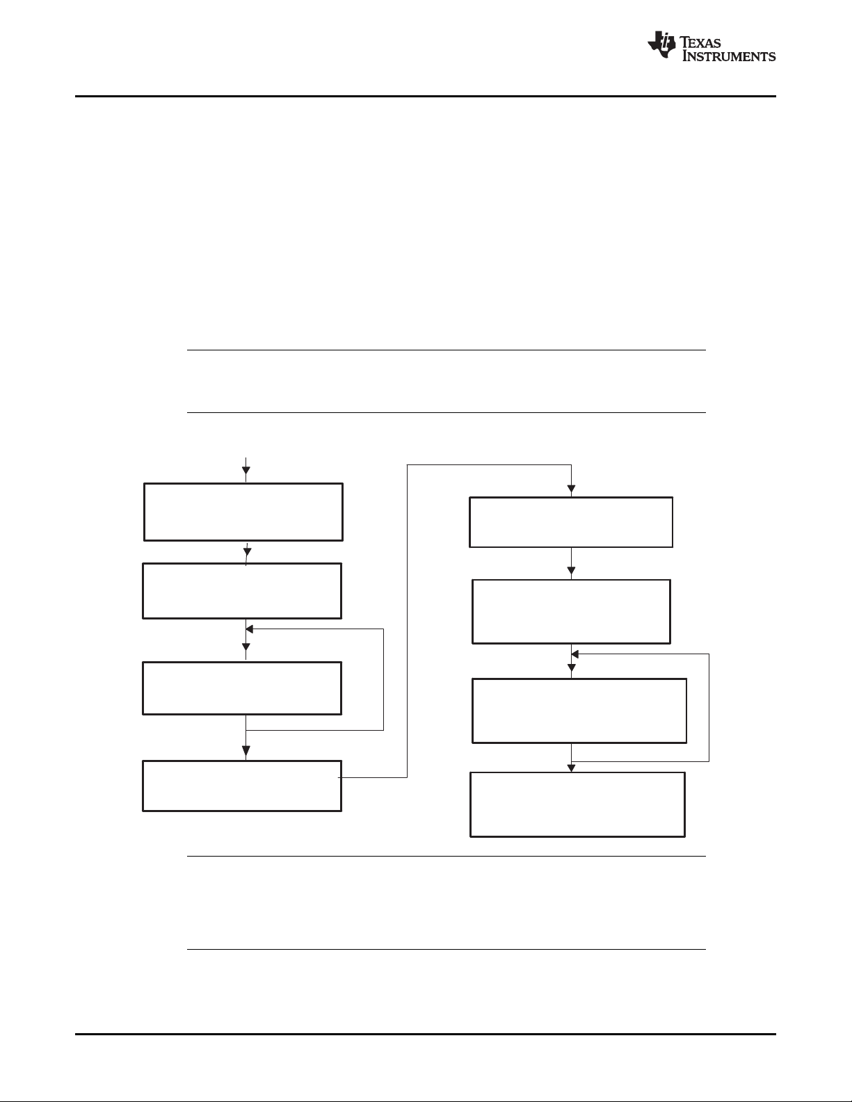
Normal mode
(CCR = 0)
(CCE = 0)
Configuration mode requested
(CCR = 1)
(CCE = 0)
Wait for configuration mode
(CCR = 1)
(CCE = 0)
CCE = 0
Configuration mode active
(CCR = 1)
(CCE = 1)
Changing of bit timing
parameters enabled
Normal mode requested
(CCR = 0)
CCE = 1
Wait for normal mode
(CCR = 0)
(CCE = 1)
CCE = 1
Initialization complete
Normal mode
CAN Module Initialization
3.1 CAN Module Initialization
www.ti.com
The CAN module must be initialized before the utilization. Initialization is only possible if the module is in
initialization mode. Figure 3-1 is a flow chart showing the process.
Programming CCR (CANMC.12) = 1 sets the initialization mode. The initialization can be performed only
when CCE (CANES.4) = 1. Afterwards, the configuration registers can be written.
SCC mode only:
In order to modify the global acceptance mask register (CANGAM) and the two local acceptance mask
registers [LAM(0) and LAM(3)], the CAN module also must be set in the initialization mode.
The module is activated again by programming CCR(CANMC.12) = 0.
After hardware reset, the initialization mode is active.
Note: If the CANBTC register is programmed with a zero value, or left with the initial value, the
CAN module never leaves the initialization mode, i.e. CCE (CANES.4) bit remains at 1 when
clearing the CCR bit.
Figure 3-1. Initialization Sequence
eCAN Configuration68 SPRU074F – May 2002 – Revised January 2009
Note: The transition between initialization mode and normal mode and vice-versa is performed in
synchronization with the CAN network. That is, the CAN controller waits until it detects a bus
idle sequence (= 11 recessive bits) before it changes the mode. In the event of a
stuck-to-dominant bus error, the CAN controller cannot detect a bus-idle condition and
therefore is unable to perform a mode transition.
Submit Documentation Feedback
Page 69

Nominal bit time
SYNCSEG
1 TQ
TSEG2TSEG1
Transmit point
Sample point
SJW SJW
Bit rate +
SYSCLKOUT
BRP Bit Time
www.ti.com
3.1.1 CAN Bit-Timing Configuration
The CAN protocol specification partitions the nominal bit time into four different time segments:
SYNC_SEG: This part of bit time is used to synchronize the various nodes on the bus. An edge is
expected to lie within this segment. This segment is always 1 TIME QUANTUM (TQ).
PROP_SEG: This part of the bit time is used to compensate for the physical delay times within the
network. It is twice the sum of the signal’s propagation ‘time on the bus line, the input comparator delay,
and the output driver delay. This segment is programmable from 1 to 8 TIME QUANTA (TQ).
PHASE_SEG1: This phase is used to compensate for positive edge phase error. This segment is
programmable from 1 to 8 TIME QUANTA (TQ) and can be lengthened by resynchronization.
PHASE_SEG2: This phase is used to compensate for negative edge phase error. This segment is
programmable from 2 to 8 TIME QUANTA (TQ) and can be shortened by resynchronization.
In the eCAN module, the length of a bit on the CAN bus is determined by the parameters TSEG1
(BTC.6-3), TSEG2 (BTC.2-0), and BRP (BTC.23.16).
TSEG1 combines the two time segments PROP_SEG and PHASE_SEG1 as defined by the CAN
protocol. TSEG2 defines the length of the time segment PHASE_SEG2.
IPT (information processing time) corresponds to the time necessary for the processing of the bit read. IPT
corresponds to two units of TQ.
The following bit timing rules must be fulfilled when determining the bit segment values:
• TSEG1(min) ≥ TSEG2
• IPT ≤ TSEG1 ≤ 16 TQ
• IPT ≤ TSEG2 ≤ 8 TQ
• IPT = 3/BRP (the resulting IPT has to be rounded up to the next integer value)
• 1 TQ ≤ SJW min[4 TQ, TSEG2] (SJW = Synchronization jump width)
• To utilize three-time sampling mode, BRP ≥ 5 has to be selected
CAN Module Initialization
3.1.2 CAN Bit Rate Calculation
Figure 3-2. CAN Bit Timing
A TSEG1 can be lengthened or TSEG2 shortened by the SJW
Bit-rate is calculated in bits per second as follows:
SPRU074F – May 2002 – Revised January 2009 eCAN Configuration 69
Submit Documentation Feedback
Page 70

Bit-time = (TSEG1
reg
+ 1) + (TSEG2
reg
+ 1) + 1
Bit-time = TSEG1 + TSEG2 + 1
CAN Module Initialization
www.ti.com
Where bit-time is the number of time quanta (TQ) per bit. SYSCLKOUT is the CAN module system clock
frequency, which is the same as the CPU clock frequency. BRP is the value of BRP
+ 1
reg
(CANBTC.23-16).
Bit-time is defined as follows:
In the above equation TESG1
and TSEG2
reg
represent the actual values written in the corresponding
reg
fields in the CANBTC register. The parameters TSEG1
automatically enhanced by 1 when the CAN module accesses these parameters. TSEG1, TSEG2 and
SJW, represent the values as applicable per Figure 3-2 .
3.1.3 Bit Configuration Parameters for 150-MHz CAN Clock
This section and Section 3.1.4 provide example values for the CANBTC bit fields for various CAN module
clocks, bit rates and sampling points. Note that these values are for illustrative purposes only. In a
real-world application, the propagation delay introduced by various entities such as the network cable,
transceivers/ isolators must be taken into account before choosing the timing parameters.
Table 3-1 shows how the BRP
80% SP.
Table 3-1. BRP Field for Bit Rates (BT = 15, TSEG1
CAN Bus Speed BRP CAN Module Clock
1 Mbps BRP
500 kbps BRP
250 kbps BRP
125 kbps BRP
100 kbps BRP
50 kbps BRP
field may be changed to achieve different bit rates with a BT of 15 for an
reg
, TSEG2r
reg
= 10, TSEG2
reg
+1 = 10 15 MHz
reg
+1 = 20 7.5 MHz
reg
+1 = 40 3.75 MHz
reg
+1 = 80 1.875 MHz
reg
+1 = 100 1.5 MHz
reg
+1 = 200 0.75 MHz
reg
, SJW
eg
, and BRP
reg
= 2, Sampling Point = 80%)
reg
are
reg
Table 3-2 shows how to achieve different sampling points with a BT of 15.
Table 3-2. Achieving Different Sampling Points With a BT of 15
TSEG1
Table 3-3 shows how BRP
reg
10 2 80%
9 3 73%
8 4 66%
7 5 60%
field may be changed to achieve different bit rates with a BT of 10 for an
reg
TSEG2
reg
80% sampling point.
Table 3-3. BRP Field for Bit Rates (BT = 10, TSEG1
CAN Bus Speed BRP CAN Module Clock
1 Mbps BRP
500 kbps BRP
250 kbps BRP
125 kbps BRP
100 kbps BRP
50 kbps BRP
reg
reg
reg
+1 = 120 1.25 MHz
reg
+1 = 150 1 MHz
reg
+1 = 300 0.5 MHz
reg
= 6, TSEG2
reg
+1 = 15 10 MHz
+1 = 30 5 MHz
+1 = 60 2.5 MHz
= 1, Sampling Point = 80%)
reg
SP
eCAN Configuration70 SPRU074F – May 2002 – Revised January 2009
Submit Documentation Feedback
Page 71

www.ti.com
3.1.4 Bit Configuration Parameters for 100-MHz CAN Clock
CAN Module Initialization
Table 3-4 shows how the BRP
field may be changed to achieve different bit rates with a BT of 10 for an
reg
80% SP.
Table 3-4. BRP Field for Bit Rates (BT = 10, TSEG1
CAN Bus Speed BRP CAN Module Clock
1 Mbps BRP
500 kbps BRP
250 kbps BRP
125 kbps BRP
100 kbps BRP
50 kbps BRP
reg
reg
reg
reg
+1 = 100 1 MHz
reg
+1 = 200 0.5 MHz
reg
= 6, TSEG2
reg
+1 = 10 10 MHz
+1 = 20 5 MHz
+1 = 40 2.5 MHz
+1 = 80 1.25 MHz
Table 3-5 shows how to achieve different sampling points with a BT of 20.
Table 3-5. Achieving Different Sampling Points With a BT of 20
TSEG1
reg
15 2 85%
14 3 80%
13 4 75%
12 5 70%
11 6 65%
10 7 60%
TSEG2
reg
= 1, Sampling Point = 80%)
reg
SP
Table 3-6 shows how BRP
field may be changed to achieve different bit rates with a BT of 20 for the
reg
sampling points shown in Table 3-5 .
Table 3-6. BRP Field for Bit Rates
CAN Bus Speed BRP
1 Mbps BRP
500 kbps BRP
250 kbps BRP
125 kbps BRP
100 kbps BRP
50 kbps BRP
Note: For a SYSCLKOUT of 150 MHz, the lowest bit-rate that can be achieved is 23.437 kbps.
For a SYSCLKOUT of 100 MHz, the lowest bit-rate that can be achieved is 15.625 kbps.
For a SYSCLKOUT of 60 MHz, the lowest bit-rate that can be achieved is 9.375 kbps.
+1 = 5
reg
+1 =10
reg
+1 = 20
reg
+1 = 40
reg
+1 = 50
reg
+1 = 100
reg
SPRU074F – May 2002 – Revised January 2009 eCAN Configuration 71
Submit Documentation Feedback
Page 72

Steps to Configure eCAN
3.1.5 EALLOW Protection
To protect against inadvertent modification, some critical registers/bits of the eCAN module are EALLOW
protected. These registers/bits can be changed only if the EALLOW protection has been disabled.
Following are the registers/ bits that are EALLOW protected in the eCAN module:
• CANMC[15..9] & MCR[7..6]
• CANBTC
• CANGIM
• MIM[31..0]
• TSC[31..0]
• IOCONT1[3]
• IOCONT2[3]
3.2 Steps to Configure eCAN
Note: This sequence must be done with EALLOW enabled.
The following steps must be performed to configure the eCAN for operation:
Step 1. Enable clock to the CAN module.
Step 2. Set the CANTX and the CANRX pins to CAN functions:
a. Write CANTIOC.3:0 = 0x08
b. Write CANRIOC.3:0 = 0x08
Step 3. After a reset, bit CCR (CANMC.12) and bit CCE (CANES.4) are set to 1. This allows the user
to configure the bit-timing configuration register (CANBTC).
If the CCE bit is set (CANES.4 = 1), proceed to next step; otherwise, set the CCR bit
(CANMC.12 = 1) and wait until CCE bit is set (CANES.4 = 1).
Step 4. Program the CANBTC register with the appropriate timing values. Make sure that the values
TSEG1 and TSEG2 are not 0. If they are 0, the module does not leave the initialization mode.
Step 5. For the SCC, program the acceptance masks now. For example:
Write LAM(3) = 0x3C0000
Step 6. Program the master control register (CANMC) as follows:
a. Clear CCR (CANMC.12) = 0
b. Clear PDR (CANMC.11) = 0
c. Clear DBO (CANMC.10) = 0
d. Clear WUBA (CANMC.9)= 0
e. Clear CDR (CANMC.8) = 0
f. Clear ABO (CANMC.7) = 0
g. Clear STM (CANMC.6) = 0
h. Clear SRES (CANMC.5) = 0
i. Clear MBNR (CANMC.4-0) = 0
Step 7. Initialize all bits of MSGCTRLn registers to zero.
Step 8. Verify the CCE bit is cleared (CANES.4 = 0), indicating that the CAN module has been
configured.
This completes the setup for the basic functionality.
www.ti.com
eCAN Configuration72 SPRU074F – May 2002 – Revised January 2009
Submit Documentation Feedback
Page 73

www.ti.com
3.2.1 Configuring a Mailbox for Transmit
To transmit a message, the following steps need to be performed (in this example, for mailbox 1):
1. Clear the appropriate bit in the CANTRS register to 0:
Clear CANTRS.1 = 0 (Writing a 0 to TRS has no effect; instead, set TRR.1 and wait until TRS.1
clears.) If the RTR bit is set, the TRS bit can send a remote frame. Once the remote frame is sent, the
TRS bit of the mailbox is cleared by the CAN module. The same node can be used to request a data
frame from another node.
2. Disable the mailbox by clearing the corresponding bit in the mailbox enable (CANME) register.
Clear CANME.filter1 = 0
3. Load the message identifier (MSGID) register of the mailbox. Clear the AME (MSGID.30) and AAM
(MSGID.29) bits for a normal send mailbox (MSGID.30 = 0 and MSGID.29 = 0). This register is usually
not modified during operation. It can only be modified when the mailbox is disabled. For example:
a. Write MSGID(1) = 0x15AC0000
b. Write the data length into the DLC field of the message control field register (MSGCTRL.3:0). The
RTR flag is usually cleared (MSGCTRL.4 = 0).
c. Set the mailbox direction by clearing the corresponding bit in the CANMD register.
d. Clear CANMD.1 = 0
4. Set the mailbox enable by setting the corresponding bit in the CANME register
Set CANME.1 = 1
This configures mailbox 1 for transmit mode.
3.2.2 Transmitting a Message
To start a transmission (in this example, for mailbox:
1. Write the message data into the mailbox data field.
a. Since DBO (MC.10) is set to zero in the configuration section and MSGCTRL(1) is set to 2, the
data are stored in the 2 MSBytes of CANMDL(1).
b. Write CANMDL(1) = xxxx0000h
2. Set the corresponding flag in the transmit request register (CANTRS.1 = 1) to start the transmission of
the message. The CAN module now handles the complete transmission of the CAN message.
3. Wait until the transmit-acknowledge flag of the corresponding mailbox is set (TA.1 = 1). After a
successful transmission, this flag is set by the CAN module.
4. The TRS flag is reset to 0 by the module after a successful or aborted transmission (TRS.1 = 0).
5. The transmit acknowledge must be cleared for the next transmission (from the same mailbox).
a. Set TA.1 = 1
b. Wait until read TA.1 is 0
6. To transmit another message in the same mailbox, the mailbox RAM data must be updated. Setting
the TRS.1 flag starts the next transmission. Writing to the mailbox RAM can be half-word (16 bits) or
full word (32 bits) but the module always returns 32-bit from even boundary. The CPU must accept all
the 32 bits or part of it.
Steps to Configure eCAN
3.2.3 Configuring Mailboxes for Receive
To configure a mailbox to receive messages, the following steps must be performed (in this example,
mailbox 3):
1. Disable the mailbox by clearing the corresponding bit in the mailbox enable (CANME) register.
Clear CANME.3 = 0
2. Write the selected identifier into the corresponding MSGID register. The identifier extension bit must be
configured to fit the expected identifier. If the acceptance mask is used, the acceptance mask enable
(AME) bit must be set (MSGID.30 = 1). For example:
Write MSGID(3) = 0x4f780000
3. If the AME bit is set to 1, the corresponding acceptance mask must be programmed.
Write LAM(3) = 0x03c0000.
SPRU074F – May 2002 – Revised January 2009 eCAN Configuration 73
Submit Documentation Feedback
Page 74

Handling of Remote Frame Mailboxes
4. Configure the mailbox as a receive mailbox by setting the corresponding flag in the mailbox direction
register (CANMD.3 = 1). Make sure no other bits in this register are affected by this operation.
5. If data in the mailbox is to be protected, the overwrite protection control register (CANOPC) should be
programmed now. This protection is useful if no message must be lost. If OPC is set, the software has
to make sure that an additional mailbox (buffer mailbox) is configured to store ’overflow’ messages.
Otherwise messages can be lost without notification.
Write OPC.3 = 1
6. Enable the mailbox by setting the appropriate flag in the mailbox enable register (CANME). This should
be done by reading CANME, and writing back (CANME |= 0x0008) to make sure no other flag has
changed accidentally.
The object is now configured for the receive mode. Any incoming message for that object is handled
automatically.
3.2.4 Receiving a Message
This example uses mailbox 3. When a message is received, the corresponding flag in the receive
message pending register (CANRMP) is set to 1 and an interrupt can be initiated. The CPU can then read
the message from the mailbox RAM. Before the CPU reads the message from the mailbox, it should first
clear the RMP bit (RMP.3 = 1). The CPU should also check the receive message lost flag RML.3 = 1.
Depending on the application, the CPU has to decide how to handle this situation.
After reading the data, the CPU needs to check that the RMP bit has not been set again by the module. If
the RMP bit has been set to 1, the data may have been corrupted. The CPU needs to read the data again
because a new message was received while the CPU was reading the old one.
www.ti.com
3.2.5 Handling of Overload Situations
If the CPU is not able to handle important messages fast enough, it may be advisable to configure more
than one mailbox for that identifier. Here is an example where the objects 3, 4, and 5 have the same
identifier and share the same mask. For the SCC, the mask is LAM(3). For the eCAN, each object has its
own LAM: LAM(3), LAM(4), and LAM(5), all of which need to be programmed with the same value.
To make sure that no message is lost, set the OPC flag for objects 4 and 5, which prevents unread
messages from being overwritten. If the CAN module must store a received message, it first checks
mailbox 5. If the mailbox is empty, the message is stored there. If the RMP flag of object 5 is set (mailbox
occupied), the CAN module checks the condition of mailbox 4. If that mailbox is also busy, the module
checks in mailbox 3 and stores the message there since the OPC flag is not set for mailbox 3. If mailbox 3
contents have not been previously read, it sets the RML flag of object 3, which can initiate an interrupt.
It is also advisable to have object 4 generate an interrupt telling the CPU to read mailboxes 4 and 5 at
once. This technique is also useful for messages that require more than 8 bytes of data (i.e., more than
one message). In this case, all data needed for the message can be collected in the mailboxes and be
read at once.
3.3 Handling of Remote Frame Mailboxes
There are two functions for remote frame handling. One is a request by the module for data from another
node, the other is a request by another node for data that the module needs to answer.
3.3.1 Requesting Data From Another Node
In order to request data from another node, the object is configured as receive mailbox. Using object 3 for
this example, the CPU needs to do the following:
1. Set the RTR bit in the message control field register (CANMSGCTRL) to 1.
Write MSGCTRL(3) = 0x12
2. Write the correct identifier into the message identifier register (MSGID).
Write MSGID(3) = 0x4F780000
74 eCAN Configuration SPRU074F – May 2002 – Revised January 2009
Submit Documentation Feedback
Page 75

www.ti.com
3. Set the CANTRS flag for that mailbox. Since the mailbox is configured as receive, it only sends a
remote request message to the other node.
Set CANTRS.3 = 1
4. The module stores the answer in that mailbox and sets the RMP bit when it is received. This action
can initiate an interrupt. Also, make sure no other mailbox has the same ID.
Wait for RMP.3 = 1
5. Read the received message.
3.3.2 Answering a Remote Request
1. Configure the object as as a transmit mailbox.
2. Set the auto answer mode (AAM) (MSGID.29) bit in the MSGID register before the mailbox is enabled.
MSGID(1) = 0x35AC0000
3. Update the data field.
MDL, MDH(1) = xxxxxxxxh
4. Enable the mailbox by setting the CANME flag to 1.
CANME.1 = 1
When a remote request is received from another node, the TRS flag is set automatically and the data
is transmitted to that node. The identifier of the received message and the transmitted message are
the same.
After transmission of the data, the TA flag is set. The CPU can then update the data.
Wait for TA.1 = 1
Interrupts
3.3.3 Updating the Data Field
To update the data of an object that is configured in auto answer mode, the following steps need to be
performed. This sequence can also be used to update the data of an object configured in normal
transmission with TRS flag set.
1. Set the change data request (CDR) (MC.8) bit and the mailbox number (MBNR) of that object in the
master control register (CANMC). This tells the CAN module that the CPU wants to change the data
field. For example, for object 1:
Write MC = 0x0000101
2. Write the message data into the mailbox data register. For example:
Write CANMDL(1) = xxxx0000h
3. Clear the CDR bit (MC.8) to enable the object.
Write MC = 0x00000000
3.4 Interrupts
There are two different types of interrupts. One type of interrupt is a mailbox related interrupt, for example,
the receive-message-pending interrupt or the abort-acknowledge interrupt. The other type of interrupt is a
system interrupt that handles errors or system-related interrupt sources, for example, the error-passive
interrupt or the wake-up interrupt. See Figure 3-3 .
The following events can initiate one of the two interrupts:
• Mailbox interrupts
– Message reception interrupt: a message was received
– Message transmission interrupt: a message was transmitted successfully
– Abort-acknowledge interrupt: a pending transmission was aborted
– Received-message-lost interrupt: an old message was overwritten by a new one (before the old
message was read)
– Mailbox timeout interrupt (eCAN mode only): one of the messages was not transmitted or received
within a predefined time frame
• System interrupts
– Write-denied interrupt: the CPU tried to write to a mailbox but was not allowed to
– Wake-up interrupt: this interrupt is generated after a wake up
SPRU074F – May 2002 – Revised January 2009 eCAN Configuration 75
Submit Documentation Feedback
Page 76

AAIF
Abort
acknowledge
Message
objects
GMIF0
System
32 transmit
or receive
mailboxes
TA [0]
RMP[0]
MIM[0]
MIL[0]
0
1
CANMIL
TA [n]
RMP[n]
MIM[n]
MIL[n]
0
1
TA [31]
RMP[31]
MIM[31]
MIL[31]
0
1
ECAN0INT
ECAN1INT
CANGIF0
GMIF1
CANGIF1
MIV0[4:0]
MIV1[4:0]
MTOF0
MTOM
MIL[n]
0
1
MTOF1
AAIF0
AAIF1
RMLIF
AAIM
0
1
Receive
message lost
WDIF0
WDIF1
WDIF
WDIM
0
1
Write
denied
WUIF0
WUIF1
WUIF
WUIM
0
1
Wake-up
BOIF0
BOIF1
BOIF
BOIM
0
1
Bus off
EPIF0
EPIF1
EPIF
EPIM
0
1
Error
passive
WLIF0
WLIF1
WLIF
WLIM
0
1
Warning
level
GIL
CANGIM
Interrupt level
select
Interrupt
masks
Interrupt
sources
Interrupt
level 0 flags
Interrupt
level 1 flags
TCOIF0
TCOIF1
TCOIF
TCOIM
0
1
Timer
overflow
RMLIF0
RMLIF1
RMLIM
0
1
CANGIM
I0EN
I1EN
Mailbox Timeout
CANMIM
Interrupts
www.ti.com
– Bus-off interrupt: the CAN module enters the bus-off state
– Error-passive interrupt: the CAN module enters the error-passive mode
– Warning level interrupt: one or both error counters are greater than or equal to 96
– Time-stamp counter overflow interrupt (eCAN only): the time-stamp counter had an overflow
Figure 3-3. Interrupts Scheme
76 eCAN Configuration SPRU074F – May 2002 – Revised January 2009
Submit Documentation Feedback
Page 77

www.ti.com
3.4.1 Interrupts Scheme
The interrupt flags are set if the corresponding interrupt condition occurred. The system interrupt flags are
set depending on the setting of GIL (CANGIM.2). If set, the global interrupts set the bits in the CANGIF1
register, otherwise they set in the CANGIF0 register.
The GMIF0/GMIF1(CANGIF0.15/CANGIF1.15) bit is set depending on the setting of the MIL[n] bit that
corresponds to the mailbox originating that interrupt. If the MIL[n] bit is set, the corresponding mailbox
interrupt flag MIF[n] sets the GMIF1 flag in the CANGIF1 register, otherwise, it sets the GMIF0 flag.
If all interrupt flags are cleared and a new interrupt flag is set, the CAN module interrupt output line
(ECAN0INT or ECAN1INT) is activated if the corresponding interrupt mask bit is set. The interrupt line
stays active until the interrupt flag is cleared by the CPU by writing a 1 to the appropriate bit.
The GMIF0 (CANGIF0.15) or GMIF1 (CANGIF0.15) bit must be cleared by writing a 1 to the appropriate
bit in the CANTA register or the CANRMP register (depending on mailbox configuration) and cannot be
cleared in the CANGIF0/CANGIF1 register.
After clearing one or more interrupt flags, and one or more interrupt flags are still pending, a new interrupt
is generated. The interrupt flags are cleared by writing a 1 to the corresponding bit location. If the GMIF0
or GMIF1 bit is set, the mailbox interrupt vector MIV0 (CANGIF0.4-0) or MIV1 (CANGIF1.4-0) indicates the
mailbox number of the mailbox that caused the setting of the GMIF0/1. It always displays the highest
mailbox interrupt vector assigned to that interrupt line.
3.4.2 Mailbox Interrupt
Each of the 32 mailboxes in the eCAN or the 16 mailboxes in the SCC can initiate an interrupt on one of
the two interrupt output lines 1 or 0. These interrupts can be receive or transmit interrupts depending on
the mailbox configuration.
There is one interrupt mask bit (MIM[n]) and one interrupt level bit (MIL[n]) dedicated to each mailbox. To
generate a mailbox interrupt upon a receive/transmit event, the MIM bit has to be set. If a CAN message
is received (RMP[n]=1) in a receive mailbox or transmitted (TA[n]=1) from a transmit mailbox, an interrupt
is asserted. If a mailbox is configured as remote request mailbox (CANMD[n]=1, MSGCTRL.RTR=1), an
interrupt occurs upon reception of the reply frame. A remote reply mailbox generates an interrupt upon
successful transmission of the reply frame (CANMD[n]=0, MSGID.AAM=1).
The setting of the RMP[n] bit or the TA[n] bit also sets the GMIF0/GMIF1 (GIF0.15/GIF1.15) flag in the
GIF0/GIF1 register if the corresponding interrupt mask bit is set. The GMIF0/GMIF1 flag then generates
an interrupt and the corresponding mailbox vector (= mailbox number) can be read from the bit field
MIV0/MIV1 in the GIF0/GIF1 register. If more than one mailbox interrupts are pending, the actual value of
MIV0/MIV1 reflects the highest priority interrupt vector. The interrupt generated depends on the setting in
the mailbox interrupt level (MIL) register.
The abort acknowledge flag (AA[n]) and the abort acknowledge interrupt flag (AAIF) in the GIF0/GIF1
register are set when a transmit message is aborted by setting the TRR[n] bit. An interrupt is asserted
upon transmission abortion if the mask bit AAIM in the GIM register is set. Clearing the AA[n] flag(s) clears
the AAIF0/AAIF1 flag.
A lost receive message is notified by setting the receive message lost flag RML[n] and the receive
message lost interrupt flag RMLIF0/RMLIF1in the GIF0/GIF1 register. If an interrupt shall be generated
upon the lost receive message event, the receive message lost interrupt mask bit (RMLIM) in the GIM
register has to be set. Clearing the RML[n] flag does not reset the RMLIF0/RMLIF1 flag. The interrupt flag
has to be cleared separately.
Each mailbox of the eCAN (in eCAN mode only) is linked to a message- object, time-out register (MOTO).
If a time-out event occurs (TOS[n] = 1), a mailbox timeout interrupt is asserted to one of the two interrupt
lines if the mailbox timeout interrupt mask bit (MTOM) in the CANGIM register is set. The interrupt line for
mailbox timeout interrupt is selected in accordance with the mailbox interrupt level (MIL[n]) of the
concerned mailbox.
Interrupts
SPRU074F – May 2002 – Revised January 2009 eCAN Configuration 77
Submit Documentation Feedback
Page 78

Interrupts
3.4.3 Interrupt Handling
www.ti.com
The CPU is interrupted by asserting one of the two interrupt lines. After handling the interrupt, which
should generally also clear the interrupt source, the interrupt flag must be cleared by the CPU. To do this,
the interrupt flag must be cleared in the CANGIF0 or CANGIF1 register. This is generally done by writing a
1 to the interrupt flag. There are some exceptions to this as stated in Table 3-7 . This also releases the
interrupt line if no other interrupt is pending.
Table 3-7. eCAN Interrupt Assertion/Clearing
Interrupt GIF0/GIF1
Flag Interrupt Condition Determination Clearing Mechanism
WLIFn One or both error counters are >= 96 GIL bit Cleared by writing a 1 to it
EPIFn CAN module has entered “error passive” GIL bit Cleared by writing a 1 to it
BOIFn CAN module has entered “bus-off” mode GIL bit Cleared by writing a 1 to it
RMLIFn An overflow condition has occurred in GIL bit Cleared by clearing the set RMPn
WUIFn CAN module has left the local power-down GIL bit Cleared by writing a 1 to it
WDIFn A write access to a mailbox was denied GIL bit Cleared by writing a 1 to it
AAIFn A transmission request was aborted GIL bit Cleared by clearing the set AAn bit.
GMIFn One of the mailboxes successfully MILn bit Cleared by appropriate handling of
TCOFn The MSB of the the TSC has changed from GIL bit Cleared by writing a 1 to it
MTOFn One of the mailboxes did not MILn bit Cleared by clearing the set TOSn
(1)
Key to interpreting the table above:
1) Interrupt flag: This is the name of the interrupt flag bit as applicable to CANGIF0/CANGIF1 registers.
2) Interrupt condition: This column illustrates the conditions that cause the interrupt to be asserted.
3) GIF0/GIF1 determination: Interrupt flag bits can be set in either CANGIF0 or CANGIF1 registers. This is determined by either
the GIL bit in CANGIM register or MILn bit in the CANMIL register, depending on the interrupt under consideration. This column
illustrates whether a particular interrupt is dependant on GIL bit or MILn bit.
4) Clearing mechanism: This column explains how a flag bit can be cleared. Some bits are cleared by writing a 1 to it. Other bits
are cleared by manipulating some other bit in the CAN control register.
mode
one of the receive mailboxes. bit.
mode
transmitted/received a message the interrupt causing condition. Cleared by
0 to 1
transmit/receive within the specified time bit.
frame.
(1)
writing a 1 to the ap-propriate bit in CANTA
or CANRMP registers
3.4.3.1 Configuring for Interrupt Handling
To configure for interrupt handling, the mailbox interrupt level register (CANMIL), the mailbox interrupt
mask register (CANMIM), and the global interrupt mask register (CANGIM) need to be configured. The
steps to do this are described below:
1. Write the CANMIL register. This defines whether a successful transmission asserts interrupt line 0 or 1.
For example, CANMIL = 0xFFFFFFFF sets all mailbox interrupts to level 1.
2. Configure the mailbox interrupt mask register (CANMIM) to mask out the mailboxes that should not
cause an interrupt. This register could be set to 0xFFFFFFFF, which enables all mailbox interrupts.
Mailboxes that are not used do not cause any interrupts anyhow.
3. Now configure the CANGIM register. The flags AAIM, WDIM, WUIM, BOIM, EPIM, and WLIM
(GIM.14-9) should always be set (enabling these interrupts). In addition, the GIL (GIM.2) bit can be set
to have the global interrupts on another level than the mailbox interrupts. Both the I1EN (GIM.1) and
I0EN (GIM.0) flags should be set to enable both interrupt lines. The flag RMLIM (GIM.11) can also be
set depending on the load of the CPU.
78 eCAN Configuration SPRU074F – May 2002 – Revised January 2009
Submit Documentation Feedback
Page 79

www.ti.com
This configuration puts all mailbox interrupts on line 1 and all system interrupts on line 0. Thus, the CPU
can handle all system interrupts (which are always serious) with high priority, and the mailbox interrupts
(on the other line) with a lower priority. All messages with a high priority can also be directed to the
interrupt line 0.
3.4.3.2 Handling Mailbox Interrupts
There are three interrupt flags for mailbox interrupts. These are listed below:
GMIF0/GMIF1: One of the objects has received or transmitted a message. The number of the mailbox is
in MIV0/MIV1(GIF0.4-0/GIF1.4-0). The normal handling routine is as follows:
1. Do a half-word read on the GIF register that caused the interrupt. If the value is negative, a mailbox
caused the interrupt. Otherwise, check the AAIF0/AAIF1 (GIF0.14/GIF1.14) bit (abort-acknowledge
interrupt flag) or the RMLIF0/RMLIF1 (GIF0.11/GIF1.11) bit (receive-message-lost interrupt flag).
Otherwise, a system interrupt has occurred. In this case, each of the system-interrupt flags must be
checked.
2. If the RMLIF (GIF0.11) flag caused the interrupt, the message in one of the mailboxes has been
overwritten by a new one. This should not happen in normal operation. The CPU needs to clear that
flag by writing a 1 to it. The CPU must check the receive-message-lost register (RML) to find out which
mailbox caused that interrupt. Depending on the application, the CPU has to decide what to do next.
This interrupt comes together with an GMIF0/GMIF1 interrupt.
3. If the AAIF (GIF.14) flag caused the interrupt, a send transmission operation was aborted by the CPU.
The CPU should check the abort acknowledge register (AA.31-0) to find out which mailbox caused the
interrupt and send that message again if requested. The flag must be cleared by writing a 1 to it.
4. If the GMIF0/GMIF1 (GIF0.15/GIF1.15) flag caused the interrupt, the mailbox number that caused the
interrupt can be read from the MIV0/MIV1 (GIF0.4-0/GIF1.4-0) field. This vector can be used to jump to
a location where that mailbox is handled. If it is a receive mailbox, the CPU should read the data as
described above and clear the RMP.31-0 flag by writing a 1 to it. If it is a send mailbox, no further
action is required, unless the CPU needs to send more data. In this case, the normal send procedure
as described above is necessary. The CPU needs to clear the transmit acknowledge bit (TA.31-0) by
writing a 1 to it.
Interrupts
3.4.3.3 Interrupt Handling Sequence
In order for the CPU core to recognize and service CAN interrupts, the following must be done in any CAN
ISR:
1. The flag bit in the CANGIF0/CANGIF1 register which caused the interrupt in the first place must be
cleared. There are two kinds of bits in these registers:
a. the very same bit that needs to be cleared. The following bits fall under this category: TCOFn,
WDIFn, WUIFn, BOIFn, EPIFn, WLIFn
b. The second group of bits are cleared by writing to the corresponding bits in the associated
registers. The following bits fall under this category: MTOFn, GMIFn, AAIFn, RMLIFn
i. The MTOFn bit is cleared by clearing the corresponding bit in the TOS register. For example, if
ii. The GMIFn bit is cleared by clearing the appropriate bit in TA or RMP register. For example, if
iii. The AAIFn bit is cleared by clearing the corresponding bit in the AA register. For example, if
iv. The RMLIFn bit is cleared by clearing the corresponding bit in the RMP register. For example, if
mailbox 27 caused a time-out condition due to which the MTOFn bit was set, the ISR (after
taking appropriate actions for the timeout condition) needs to clear the TOS27 bit in order to
clear the MTOFn bit.
mailbox 19 has been configured as a transmit mailbox and has completed a transmission,
TA19 is set, which in turn sets GMIFn. The ISR (after taking appropriate actions) needs to clear
the TA19 bit in order to clear the GMIFn bit. If mailbox 8 has been configured as a receive
mailbox and has completed a reception, RMP8 is set, which in turn sets GMIFn. The ISR (after
taking appropriate actions) needs to clear the RMP8 bit in order to clear the GMIFn bit.
mailbox 13’s transmission was aborted due to which the AAIFn bit was set, the ISR needs to
clear the AA13 bit in order to clear the AAIFn bit.
mailbox 13’s message was overwritten due to which the RMLIFn bit was set, the ISR needs to
clear the RMP13 bit in order to clear the RMLIFn bit.
SPRU074F – May 2002 – Revised January 2009 eCAN Configuration 79
Submit Documentation Feedback
Page 80

CAN Power-Down Mode
2. The PIEACK bit corresponding corresponding to the CAN module must be written with a 1, which can
be accomplished with the following C language statement:
PieCtrlRegs.PIEACK.bit.ACK9 = 1; // Enables PIE to drive a pulse into the CPU
3. The interrupt line into the CPU corresponding to the CAN module must be enabled, which can be
accomplished with the following C language statement:
IER |= 0x0100; // Enable INT9
4. The CPU interrupts must be enabled globally by clearing the INTM bit.
3.5 CAN Power-Down Mode
A local power-down mode has been implemented where the CAN module internal clock is de-activated by
the CAN module itself.
3.5.1 Entering and Exiting Local Power-Down Mode
During local power-down mode, the clock of the CAN module is turned off (by the CAN module itself) and
only the wake-up logic is still active. The other peripherals continue to operate normally.
The local power-down mode is requested by writing a 1 to the PDR (CANMC.11) bit, allowing transmission
of any packet in progress to complete. After the transmission is completed, the status bit PDA (CANES.3)
is set. This confirms that the CAN module has entered the power-down mode.
The value read on the CANES register is 0x08 (PDA bit is set). All other register read accesses deliver the
value 0x00.
The module leaves the local power-down mode when the PDR bit is cleared or if any bus activity is
detected on the CAN bus line (if the wake-up-on bus activity is enabled).
The automatic wake-up-on bus activity can be enabled or disabled with the configuration bit WUBA of
CANMC register. If there is any activity on the CAN bus line, the module begins its power-up sequence.
The module waits until it detects 11 consecutive recessive bits on the CANRX pin and then it goes
bus-active.
www.ti.com
Note: The first CAN message, which initiates the bus activity, cannot be received. This means that
the first message received in power-down and automatic wake-up mode is lost.
After leaving the sleep mode, the PDR and PDA bits are cleared. The CAN error counters remain
unchanged.
If the module is transmitting a message when the PDR bit is set, the transmission is continued until a
successful transmission, a lost arbitration, or an error condition on the CAN bus line occurs. Then, the
PDA bit is activated so the module causes no error condition on the CAN bus line.
To implement the local power-down mode, two separate clocks are used within the CAN module. One
clock stays active all the time to ensure power-down operation (i.e., the wake-up logic and the write and
read access to the PDA (CANES.3) bit). The other clock is enabled depending on the setting of the PDR
bit.
3.5.2 Precautions for Entering and Exiting Device Low-Power Modes (LPM)
The 28x DSP features two low-power modes, STANDBY and HALT, in which the peripheral clocks are
turned off. Since the CAN module is connected to multiple nodes across a network, you must take care
before entering and exiting device low-power modes such as STANDBY and HALT. A CAN packet must
be received in full by all the nodes; therefore, if transmission is aborted half-way through the process, the
aborted packet would violate the CAN protocol resulting in all the nodes generating error frames. The
node exiting LPM should do so unobtrusively. For example, if a node exits LPM when there is traffic on
the CAN bus it could “see” a truncated packet and disturb the bus with error frames.
The following points must be considered before entering a device low-power mode:
1. The CAN module has completed the transmission of the last packet requested.
80 eCAN Configuration SPRU074F – May 2002 – Revised January 2009
Submit Documentation Feedback
Page 81

www.ti.com
2. The CAN module has signaled to the CPU that it is ready to enter LPM.
In other words, device low-power modes should be entered into only after putting the CAN module in local
power-down mode.
3.5.3 Enabling/Disabling Clock to the CAN Module
The CAN module cannot be used unless the clock to the module is enabled. It is enabled or disabled by
using bit 14 of the PCLKCR register. This bit is useful in applications that do not use the CAN module at
all. In such applications, the CAN module clock can be permanently turned off, resulting in some power
saving. This bit is not intended to put the CAN module in low-power mode and should not be used for that
purpose. Like all other peripherals, clock to the CAN module is disabled upon reset.
3.5.4 Possible Failure Modes External to the CAN Controller Module
This section lists some potential failure modes in a CAN based system. The failure modes listed are
external to the CAN controller and hence, need to be evaluated at the system level.
• CAN_H and CAN_ L shorted together
• CAN_H and/or CAN_ L shorted to ground
• CAN_H and/or CAN_ L shorted to supply
• Failed CAN transceiver
• Electrical disturbance on CAN bus
CAN Power-Down Mode
SPRU074F – May 2002 – Revised January 2009 eCAN Configuration 81
Submit Documentation Feedback
Page 82

eCAN Configuration82 SPRU074F – May 2002 – Revised January 2009
Submit Documentation Feedback
Page 83

Appendix A
SPRU074F – May 2002 – Revised January 2009
Revision History
This document was revised to SPRU074F from SPRU074E. The scope of the revisions was limited to
technical changes as described in Table A-1 . This appendix lists only revisions made in the most recent
version.
Table A-1. Changes Made in This Revision
Reference Additions/Modifications/Deletions
Global change all " < device> CAN" to "eCAN"
NoLabel Device name change from TMS320x28xx, 28xxx DSP to TMS320x281x
Chapter 1 Changed 1st paragraph
Chapter 1 Changed 2nd paragraph
Figure 1-1 changed Figure
Section 1.3 Added to 5th paragraph ("To initiate...")
Section 1.3.2.1 Added this section
Section 1.5.3 Added last sentence in 1st paragraph
Section 1.5.3 Added 3rd paragraph
Table 2-1 Changed field description
Table 2-2 Changed field description
Table 2-12 Changed bits [23:16] and [9:8] descriptions
Section 2.18.1 Changed "MSCC" to "MBCC" in 3rd paragraph
Table 2-26 Removed the note in bit 31s description
Table 2-14 Changed bit 13 description
Section 1.5.3 Changed last Paragraph
Section 2.13 Changed first paragraph
Section 3.1.3 Changed first sentence
Section 3.1.4 Changed section title
SPRU074F – May 2002 – Revised January 2009 Revision History 83
Submit Documentation Feedback
Page 84

IMPORTANT NOTICE
Texas Instruments Incorporated and its subsidiaries (TI) reserve the right to make corrections, modifications, enhancements, improvements,
and other changes to its products and services at any time and to discontinue any product or service without notice. Customers should
obtain the latest relevant information before placing orders and should verify that such information is current and complete. All products are
sold subject to TI’s terms and conditions of sale supplied at the time of order acknowledgment.
TI warrants performance of its hardware products to the specifications applicable at the time of sale in accordance with TI’s standard
warranty. Testing and other quality control techniques are used to the extent TI deems necessary to support this warranty. Except where
mandated by government requirements, testing of all parameters of each product is not necessarily performed.
TI assumes no liability for applications assistance or customer product design. Customers are responsible for their products and
applications using TI components. To minimize the risks associated with customer products and applications, customers should provide
adequate design and operating safeguards.
TI does not warrant or represent that any license, either express or implied, is granted under any TI patent right, copyright, mask work right,
or other TI intellectual property right relating to any combination, machine, or process in which TI products or services are used. Information
published by TI regarding third-party products or services does not constitute a license from TI to use such products or services or a
warranty or endorsement thereof. Use of such information may require a license from a third party under the patents or other intellectual
property of the third party, or a license from TI under the patents or other intellectual property of TI.
Reproduction of TI information in TI data books or data sheets is permissible only if reproduction is without alteration and is accompanied
by all associated warranties, conditions, limitations, and notices. Reproduction of this information with alteration is an unfair and deceptive
business practice. TI is not responsible or liable for such altered documentation. Information of third parties may be subject to additional
restrictions.
Resale of TI products or services with statements different from or beyond the parameters stated by TI for that product or service voids all
express and any implied warranties for the associated TI product or service and is an unfair and deceptive business practice. TI is not
responsible or liable for any such statements.
TI products are not authorized for use in safety-critical applications (such as life support) where a failure of the TI product would reasonably
be expected to cause severe personal injury or death, unless officers of the parties have executed an agreement specifically governing
such use. Buyers represent that they have all necessary expertise in the safety and regulatory ramifications of their applications, and
acknowledge and agree that they are solely responsible for all legal, regulatory and safety-related requirements concerning their products
and any use of TI products in such safety-critical applications, notwithstanding any applications-related information or support that may be
provided by TI. Further, Buyers must fully indemnify TI and its representatives against any damages arising out of the use of TI products in
such safety-critical applications.
TI products are neither designed nor intended for use in military/aerospace applications or environments unless the TI products are
specifically designated by TI as military-grade or "enhanced plastic." Only products designated by TI as military-grade meet military
specifications. Buyers acknowledge and agree that any such use of TI products which TI has not designated as military-grade is solely at
the Buyer's risk, and that they are solely responsible for compliance with all legal and regulatory requirements in connection with such use.
TI products are neither designed nor intended for use in automotive applications or environments unless the specific TI products are
designated by TI as compliant with ISO/TS 16949 requirements. Buyers acknowledge and agree that, if they use any non-designated
products in automotive applications, TI will not be responsible for any failure to meet such requirements.
Following are URLs where you can obtain information on other Texas Instruments products and application solutions:
Products Applications
Amplifiers amplifier.ti.com Audio www.ti.com/audio
Data Converters dataconverter.ti.com Automotive www.ti.com/automotive
DLP® Products www.dlp.com Broadband www.ti.com/broadband
DSP dsp.ti.com Digital Control www.ti.com/digitalcontrol
Clocks and Timers www.ti.com/clocks Medical www.ti.com/medical
Interface interface.ti.com Military www.ti.com/military
Logic logic.ti.com Optical Networking www.ti.com/opticalnetwork
Power Mgmt power.ti.com Security www.ti.com/security
Microcontrollers microcontroller.ti.com Telephony www.ti.com/telephony
RFID www.ti-rfid.com Video & Imaging www.ti.com/video
RF/IF and ZigBee® Solutions www.ti.com/lprf Wireless www.ti.com/wireless
Mailing Address: Texas Instruments, Post Office Box 655303, Dallas, Texas 75265
Copyright © 2009, Texas Instruments Incorporated
 Loading...