

Page 1

TMS320VC5509 Fixed-Point
Digital Signal Processor
Data Manual
Literature Number: SPRS163H
April 2001 − Revised January 2008
!
!
Page 2

This page intentionally left blank
Page 3

REVISION HISTORY
This revision history highlights the technical changes made to SPRS163G to generate SPRS163H.
Scope:
Revision History
PAGE(S)
NO.
18 Table 2−3, Signal Descriptions (Continued):
− Updated/changed D[15:0] FUNCTION description from “... The data bus keepers are disabled at reset, ...” to “... The
data bus keepers are enabled at reset, ...”.
ADDITIONS/CHANGES/DELETIONS
April 2001 − Revised January 2008 SPRS163H
3
Page 4

Revision History
This page intentionally left blank
4
April 2001 − Revised January 2008SPRS163H
Page 5

Contents
Contents
Section Page
1 TMS320VC5509 Features 11. . . . . . . . . . . . . . . . . . . . . . . . . . . . . . . . . . . . . . . . . . . . . . . . . . . . . . . . . . . . . . . .
2 Introduction 12. . . . . . . . . . . . . . . . . . . . . . . . . . . . . . . . . . . . . . . . . . . . . . . . . . . . . . . . . . . . . . . . . . . . . . . . . . . .
2.1 Description 12. . . . . . . . . . . . . . . . . . . . . . . . . . . . . . . . . . . . . . . . . . . . . . . . . . . . . . . . . . . . . . . . . . . . . .
2.2 Pin Assignments 13. . . . . . . . . . . . . . . . . . . . . . . . . . . . . . . . . . . . . . . . . . . . . . . . . . . . . . . . . . . . . . . . . .
2.2.1 Terminal Assignments for the GHH Package 13. . . . . . . . . . . . . . . . . . . . . . . . . . . . . . . .
2.2.2 Pin Assignments for the PGE Package 15. . . . . . . . . . . . . . . . . . . . . . . . . . . . . . . . . . . . .
2.3 Signal Descriptions 17. . . . . . . . . . . . . . . . . . . . . . . . . . . . . . . . . . . . . . . . . . . . . . . . . . . . . . . . . . . . . . .
3 Functional Overview 30. . . . . . . . . . . . . . . . . . . . . . . . . . . . . . . . . . . . . . . . . . . . . . . . . . . . . . . . . . . . . . . . . . . .
3.1 Memory 31. . . . . . . . . . . . . . . . . . . . . . . . . . . . . . . . . . . . . . . . . . . . . . . . . . . . . . . . . . . . . . . . . . . . . . . . .
3.1.1 On-Chip Dual-Access RAM (DARAM) 31. . . . . . . . . . . . . . . . . . . . . . . . . . . . . . . . . . . . . .
3.1.2 On-Chip Single-Access RAM (SARAM) 31. . . . . . . . . . . . . . . . . . . . . . . . . . . . . . . . . . . .
3.1.3 On-Chip Read-Only Memory (ROM) 32. . . . . . . . . . . . . . . . . . . . . . . . . . . . . . . . . . . . . . .
3.1.4 Secure ROM 32. . . . . . . . . . . . . . . . . . . . . . . . . . . . . . . . . . . . . . . . . . . . . . . . . . . . . . . . . . .
3.1.5 Memory Map 33. . . . . . . . . . . . . . . . . . . . . . . . . . . . . . . . . . . . . . . . . . . . . . . . . . . . . . . . . . .
3.1.6 Boot Configuration 36. . . . . . . . . . . . . . . . . . . . . . . . . . . . . . . . . . . . . . . . . . . . . . . . . . . . . .
3.2 Peripherals 37. . . . . . . . . . . . . . . . . . . . . . . . . . . . . . . . . . . . . . . . . . . . . . . . . . . . . . . . . . . . . . . . . . . . . .
3.3 Direct Memory Access (DMA) Controller 37. . . . . . . . . . . . . . . . . . . . . . . . . . . . . . . . . . . . . . . . . . . . .
3.3.1 DMA Channel Control Register (DMA_CCR) 38. . . . . . . . . . . . . . . . . . . . . . . . . . . . . . . .
3.4 I2C Interface 39. . . . . . . . . . . . . . . . . . . . . . . . . . . . . . . . . . . . . . . . . . . . . . . . . . . . . . . . . . . . . . . . . . . . .
3.5 Configurable External Buses 40. . . . . . . . . . . . . . . . . . . . . . . . . . . . . . . . . . . . . . . . . . . . . . . . . . . . . . .
3.5.1 External Bus Selection Register 40. . . . . . . . . . . . . . . . . . . . . . . . . . . . . . . . . . . . . . . . . . .
3.5.2 Parallel Port 42. . . . . . . . . . . . . . . . . . . . . . . . . . . . . . . . . . . . . . . . . . . . . . . . . . . . . . . . . . . .
3.5.3 Parallel Port Signal Routing 43. . . . . . . . . . . . . . . . . . . . . . . . . . . . . . . . . . . . . . . . . . . . . . .
3.5.4 Serial Ports 44. . . . . . . . . . . . . . . . . . . . . . . . . . . . . . . . . . . . . . . . . . . . . . . . . . . . . . . . . . . . .
3.6 General-Purpose Input/Output (GPIO) Ports 45. . . . . . . . . . . . . . . . . . . . . . . . . . . . . . . . . . . . . . . . .
3.6.1 Dedicated General-Purpose I/O 45. . . . . . . . . . . . . . . . . . . . . . . . . . . . . . . . . . . . . . . . . . .
3.6.2 Address Bus General-Purpose I/O 46. . . . . . . . . . . . . . . . . . . . . . . . . . . . . . . . . . . . . . . . .
3.6.3 EHPI General-Purpose I/O 48. . . . . . . . . . . . . . . . . . . . . . . . . . . . . . . . . . . . . . . . . . . . . . .
3.7 System Register 49. . . . . . . . . . . . . . . . . . . . . . . . . . . . . . . . . . . . . . . . . . . . . . . . . . . . . . . . . . . . . . . . . .
3.8 Memory-Mapped Registers 50. . . . . . . . . . . . . . . . . . . . . . . . . . . . . . . . . . . . . . . . . . . . . . . . . . . . . . . .
3.9 Peripheral Register Description 52. . . . . . . . . . . . . . . . . . . . . . . . . . . . . . . . . . . . . . . . . . . . . . . . . . . . .
3.10 Interrupts 65. . . . . . . . . . . . . . . . . . . . . . . . . . . . . . . . . . . . . . . . . . . . . . . . . . . . . . . . . . . . . . . . . . . . . . . .
3.10.1 IFR and IER Registers 66. . . . . . . . . . . . . . . . . . . . . . . . . . . . . . . . . . . . . . . . . . . . . . . . . . .
3.10.2 Interrupt Timing 67. . . . . . . . . . . . . . . . . . . . . . . . . . . . . . . . . . . . . . . . . . . . . . . . . . . . . . . . .
3.10.3 Waking Up From IDLE Condition 68. . . . . . . . . . . . . . . . . . . . . . . . . . . . . . . . . . . . . . . . . .
3.10.4 Idling Clock Domain When External Parallel Bus Operating in EHPI Mode 68. . . . . .
4 Documentation Support 69. . . . . . . . . . . . . . . . . . . . . . . . . . . . . . . . . . . . . . . . . . . . . . . . . . . . . . . . . . . . . . . . .
4.1 Device and Development-Support Tool Nomenclature 70. . . . . . . . . . . . . . . . . . . . . . . . . . . . . . . . .
4.2 TMS320VC5509 Device Nomenclature 71. . . . . . . . . . . . . . . . . . . . . . . . . . . . . . . . . . . . . . . . . . . . . .
April 2001 − Revised January 2008 SPRS163H
5
Page 6

Contents
Section Page
5 Electrical Specifications 72. . . . . . . . . . . . . . . . . . . . . . . . . . . . . . . . . . . . . . . . . . . . . . . . . . . . . . . . . . . . . . . .
5.1 Absolute Maximum Ratings 72. . . . . . . . . . . . . . . . . . . . . . . . . . . . . . . . . . . . . . . . . . . . . . . . . . . . . . . .
5.2 Recommended Operating Conditions 72. . . . . . . . . . . . . . . . . . . . . . . . . . . . . . . . . . . . . . . . . . . . . . .
5.3 Electrical Characteristics Over Recommended Operating Case Temperature Range 74. . . . . . .
5.4 Package Thermal Resistance Characteristics 75. . . . . . . . . . . . . . . . . . . . . . . . . . . . . . . . . . . . . . . . .
5.5 Timing Parameter Symbology 76. . . . . . . . . . . . . . . . . . . . . . . . . . . . . . . . . . . . . . . . . . . . . . . . . . . . . .
5.6 Clock Options 77. . . . . . . . . . . . . . . . . . . . . . . . . . . . . . . . . . . . . . . . . . . . . . . . . . . . . . . . . . . . . . . . . . . .
5.6.1 Internal System Oscillator With External Crystal 77. . . . . . . . . . . . . . . . . . . . . . . . . . . . .
5.6.2 Layout Considerations 78. . . . . . . . . . . . . . . . . . . . . . . . . . . . . . . . . . . . . . . . . . . . . . . . . . .
5.6.3 Clock Generation in Bypass Mode (DPLL Disabled) 78. . . . . . . . . . . . . . . . . . . . . . . . . .
5.6.4 Clock Generation in Lock Mode (DPLL Synthesis Enabled) 79. . . . . . . . . . . . . . . . . . .
5.6.5 Real-Time Clock Oscillator With External Crystal 80. . . . . . . . . . . . . . . . . . . . . . . . . . . .
5.7 Memory Interface Timings 81. . . . . . . . . . . . . . . . . . . . . . . . . . . . . . . . . . . . . . . . . . . . . . . . . . . . . . . . .
5.7.1 Asynchronous Memory Timings 81. . . . . . . . . . . . . . . . . . . . . . . . . . . . . . . . . . . . . . . . . . .
5.7.2 Synchronous DRAM (SDRAM) Timings 84. . . . . . . . . . . . . . . . . . . . . . . . . . . . . . . . . . . .
5.8 Reset Timings 92. . . . . . . . . . . . . . . . . . . . . . . . . . . . . . . . . . . . . . . . . . . . . . . . . . . . . . . . . . . . . . . . . . . .
5.8.1 Power-Up Reset (On-Chip Oscillator Active) 92. . . . . . . . . . . . . . . . . . . . . . . . . . . . . . . .
5.8.2 Power-Up Reset (On-Chip Oscillator Inactive) 92. . . . . . . . . . . . . . . . . . . . . . . . . . . . . . .
5.8.3 Warm Reset 93. . . . . . . . . . . . . . . . . . . . . . . . . . . . . . . . . . . . . . . . . . . . . . . . . . . . . . . . . . . .
5.9 External Interrupt Timings 94. . . . . . . . . . . . . . . . . . . . . . . . . . . . . . . . . . . . . . . . . . . . . . . . . . . . . . . . . .
5.10 Wake-Up From IDLE 94. . . . . . . . . . . . . . . . . . . . . . . . . . . . . . . . . . . . . . . . . . . . . . . . . . . . . . . . . . . . . .
5.11 XF Timings 95. . . . . . . . . . . . . . . . . . . . . . . . . . . . . . . . . . . . . . . . . . . . . . . . . . . . . . . . . . . . . . . . . . . . . .
5.12 General-Purpose Input/Output (GPIOx) Timings 96. . . . . . . . . . . . . . . . . . . . . . . . . . . . . . . . . . . . . .
5.13 TIN/TOUT Timings (Timer0 Only) 97. . . . . . . . . . . . . . . . . . . . . . . . . . . . . . . . . . . . . . . . . . . . . . . . . . .
5.14 Multichannel Buffered Serial Port (McBSP) Timings 98. . . . . . . . . . . . . . . . . . . . . . . . . . . . . . . . . . .
5.14.1 McBSP Transmit and Receive Timings 98. . . . . . . . . . . . . . . . . . . . . . . . . . . . . . . . . . . . .
5.14.2 McBSP General-Purpose I/O Timings 101. . . . . . . . . . . . . . . . . . . . . . . . . . . . . . . . . . . . . .
5.14.3 McBSP as SPI Master or Slave Timings 102. . . . . . . . . . . . . . . . . . . . . . . . . . . . . . . . . . . .
5.15 Enhanced Host-Port Interface (EHPI) Timings 107. . . . . . . . . . . . . . . . . . . . . . . . . . . . . . . . . . . . . . . .
2
5.16 I
C Timings 113. . . . . . . . . . . . . . . . . . . . . . . . . . . . . . . . . . . . . . . . . . . . . . . . . . . . . . . . . . . . . . . . . . . . . .
5.17 MultiMedia Card (MMC) Timings 115. . . . . . . . . . . . . . . . . . . . . . . . . . . . . . . . . . . . . . . . . . . . . . . . . . . .
5.18 Secure Digital (SD) Card Timings 116. . . . . . . . . . . . . . . . . . . . . . . . . . . . . . . . . . . . . . . . . . . . . . . . . . .
5.19 Universal Serial Bus (USB) Timings 117. . . . . . . . . . . . . . . . . . . . . . . . . . . . . . . . . . . . . . . . . . . . . . . . .
5.20 ADC Timings 119. . . . . . . . . . . . . . . . . . . . . . . . . . . . . . . . . . . . . . . . . . . . . . . . . . . . . . . . . . . . . . . . . . . . .
6 Mechanical Data 120. . . . . . . . . . . . . . . . . . . . . . . . . . . . . . . . . . . . . . . . . . . . . . . . . . . . . . . . . . . . . . . . . . . . . . . .
6
April 2001 − Revised January 2008SPRS163H
Page 7

Figures
List of Figures
Figure Page
2−1 179-Terminal GHH Ball Grid Array (Bottom View) 13. . . . . . . . . . . . . . . . . . . . . . . . . . . . . . . . . . . . . . . . .
2−2 144-Pin PGE Low-Profile Quad Flatpack (Top View) 15. . . . . . . . . . . . . . . . . . . . . . . . . . . . . . . . . . . . . .
3−1 Block Diagram of the TMS320VC5509 30. . . . . . . . . . . . . . . . . . . . . . . . . . . . . . . . . . . . . . . . . . . . . . . . . .
3−2 Secure ROM 32. . . . . . . . . . . . . . . . . . . . . . . . . . . . . . . . . . . . . . . . . . . . . . . . . . . . . . . . . . . . . . . . . . . . . . . .
3−3 TMS320VC5509 Memory Map (PGE Package) 34. . . . . . . . . . . . . . . . . . . . . . . . . . . . . . . . . . . . . . . . . . .
3−4 TMS320VC5509 Memory Map (GHH Package) 35. . . . . . . . . . . . . . . . . . . . . . . . . . . . . . . . . . . . . . . . . .
3−5 DMA_CCR Bit Locations 38. . . . . . . . . . . . . . . . . . . . . . . . . . . . . . . . . . . . . . . . . . . . . . . . . . . . . . . . . . . . . .
3−6 External Bus Selection Register 40. . . . . . . . . . . . . . . . . . . . . . . . . . . . . . . . . . . . . . . . . . . . . . . . . . . . . . . .
3−7 Parallel Port Signal Routing 43. . . . . . . . . . . . . . . . . . . . . . . . . . . . . . . . . . . . . . . . . . . . . . . . . . . . . . . . . . . .
3−8 Parallel Port (EMIF) Signal Interface 44. . . . . . . . . . . . . . . . . . . . . . . . . . . . . . . . . . . . . . . . . . . . . . . . . . . .
3−9 I/O Direction Register (IODIR) Bit Layout 45. . . . . . . . . . . . . . . . . . . . . . . . . . . . . . . . . . . . . . . . . . . . . . . .
3−10 I/O Data Register (IODATA) Bit Layout 46. . . . . . . . . . . . . . . . . . . . . . . . . . . . . . . . . . . . . . . . . . . . . . . . . .
3−11 Address/GPIO Enable Register (AGPIOEN) Bit Layout 46. . . . . . . . . . . . . . . . . . . . . . . . . . . . . . . . . . . .
3−12 Address/GPIO Direction Register (AGPIODIR) Bit Layout 47. . . . . . . . . . . . . . . . . . . . . . . . . . . . . . . . . .
3−13 Address/GPIO Data Register (AGPIODATA) Bit Layout 47. . . . . . . . . . . . . . . . . . . . . . . . . . . . . . . . . . . .
3−14 EHPI GPIO Enable Register (EHPIGPIOEN) Bit Layout 48. . . . . . . . . . . . . . . . . . . . . . . . . . . . . . . . . . .
3−15 EHPI GPIO Direction Register (EHPIGPIODIR) Bit Layout 48. . . . . . . . . . . . . . . . . . . . . . . . . . . . . . . . .
3−16 EHPI GPIO Data Register (EHPIGPIODATA) Bit Layout 49. . . . . . . . . . . . . . . . . . . . . . . . . . . . . . . . . . .
3−17 IFR0 and IER0 Bit Locations 66. . . . . . . . . . . . . . . . . . . . . . . . . . . . . . . . . . . . . . . . . . . . . . . . . . . . . . . . . . .
3−18 IFR1 and IER1 Bit Locations 67. . . . . . . . . . . . . . . . . . . . . . . . . . . . . . . . . . . . . . . . . . . . . . . . . . . . . . . . . . .
4−1 Device Nomenclature for the TMS320VC5509 71. . . . . . . . . . . . . . . . . . . . . . . . . . . . . . . . . . . . . . . . . . .
5−1 3.3-V Test Load Circuit 75. . . . . . . . . . . . . . . . . . . . . . . . . . . . . . . . . . . . . . . . . . . . . . . . . . . . . . . . . . . . . . . .
5−2 Internal System Oscillator With External Crystal 77. . . . . . . . . . . . . . . . . . . . . . . . . . . . . . . . . . . . . . . . . .
5−3 Bypass Mode Clock Timings 79. . . . . . . . . . . . . . . . . . . . . . . . . . . . . . . . . . . . . . . . . . . . . . . . . . . . . . . . . . .
5−4 External Multiply-by-N Clock Timings 80. . . . . . . . . . . . . . . . . . . . . . . . . . . . . . . . . . . . . . . . . . . . . . . . . . . .
5−5 Real-Time Clock Oscillator With External Crystal 80. . . . . . . . . . . . . . . . . . . . . . . . . . . . . . . . . . . . . . . . .
5−6 Asynchronous Memory Read Timings 82. . . . . . . . . . . . . . . . . . . . . . . . . . . . . . . . . . . . . . . . . . . . . . . . . . .
5−7 Asynchronous Memory Write Timings 83. . . . . . . . . . . . . . . . . . . . . . . . . . . . . . . . . . . . . . . . . . . . . . . . . . .
5−8 Three SDRAM Read Commands 86. . . . . . . . . . . . . . . . . . . . . . . . . . . . . . . . . . . . . . . . . . . . . . . . . . . . . . .
5−9 Three SDRAM WRT Commands 87. . . . . . . . . . . . . . . . . . . . . . . . . . . . . . . . . . . . . . . . . . . . . . . . . . . . . . .
5−10 SDRAM ACTV Command 88. . . . . . . . . . . . . . . . . . . . . . . . . . . . . . . . . . . . . . . . . . . . . . . . . . . . . . . . . . . . .
5−11 SDRAM DCAB Command 89. . . . . . . . . . . . . . . . . . . . . . . . . . . . . . . . . . . . . . . . . . . . . . . . . . . . . . . . . . . . .
5−12 SDRAM REFR Command 90. . . . . . . . . . . . . . . . . . . . . . . . . . . . . . . . . . . . . . . . . . . . . . . . . . . . . . . . . . . . .
5−13 SDRAM MRS Command 91. . . . . . . . . . . . . . . . . . . . . . . . . . . . . . . . . . . . . . . . . . . . . . . . . . . . . . . . . . . . . .
5−14 Power-Up Reset (On-Chip Oscillator Active) Timings 92. . . . . . . . . . . . . . . . . . . . . . . . . . . . . . . . . . . . . .
5−15 Power-Up Reset (On-Chip Oscillator Inactive) Timings 92. . . . . . . . . . . . . . . . . . . . . . . . . . . . . . . . . . . .
5−16 Reset Timings 93. . . . . . . . . . . . . . . . . . . . . . . . . . . . . . . . . . . . . . . . . . . . . . . . . . . . . . . . . . . . . . . . . . . . . . .
April 2001 − Revised January 2008 SPRS163H
7
Page 8

Figures
Figure Page
5−17 External Interrupt Timings 94. . . . . . . . . . . . . . . . . . . . . . . . . . . . . . . . . . . . . . . . . . . . . . . . . . . . . . . . . . . . .
5−18 Wake-Up From IDLE Timings 94. . . . . . . . . . . . . . . . . . . . . . . . . . . . . . . . . . . . . . . . . . . . . . . . . . . . . . . . . .
5−19 XF Timings 95. . . . . . . . . . . . . . . . . . . . . . . . . . . . . . . . . . . . . . . . . . . . . . . . . . . . . . . . . . . . . . . . . . . . . . . . . .
5−20 General-Purpose Input/Output (IOx) Signal Timings 96. . . . . . . . . . . . . . . . . . . . . . . . . . . . . . . . . . . . . . .
5−21 TIN/TOUT Timings When Configured as Inputs 97. . . . . . . . . . . . . . . . . . . . . . . . . . . . . . . . . . . . . . . . . . .
5−22 TIN/TOUT Timings When Configured as Outputs 97. . . . . . . . . . . . . . . . . . . . . . . . . . . . . . . . . . . . . . . . .
5−23 McBSP Receive Timings 100. . . . . . . . . . . . . . . . . . . . . . . . . . . . . . . . . . . . . . . . . . . . . . . . . . . . . . . . . . . . . .
5−24 McBSP Transmit Timings 100. . . . . . . . . . . . . . . . . . . . . . . . . . . . . . . . . . . . . . . . . . . . . . . . . . . . . . . . . . . . . .
5−25 McBSP General-Purpose I/O Timings 101. . . . . . . . . . . . . . . . . . . . . . . . . . . . . . . . . . . . . . . . . . . . . . . . . . .
5−26 McBSP Timings as SPI Master or Slave: CLKSTP = 10b, CLKXP = 0 103. . . . . . . . . . . . . . . . . . . . . . .
5−27 McBSP Timings as SPI Master or Slave: CLKSTP = 11b, CLKXP = 0 104. . . . . . . . . . . . . . . . . . . . . . .
5−28 McBSP Timings as SPI Master or Slave: CLKSTP = 10b, CLKXP = 1 105. . . . . . . . . . . . . . . . . . . . . . .
5−29 McBSP Timings as SPI Master or Slave: CLKSTP = 11b, CLKXP = 1 106. . . . . . . . . . . . . . . . . . . . . . .
5−30 EHPI Nonmultiplexed Read/Write Timings 108. . . . . . . . . . . . . . . . . . . . . . . . . . . . . . . . . . . . . . . . . . . . . . .
5−31 EHPI Multiplexed Memory (HPID) Access Read/Write Timings Without Autoincrement 109. . . . . . . . .
5−32 EHPI Multiplexed Memory (HPID) Access Read Timings With Autoincrement 110. . . . . . . . . . . . . . . . .
5−33 EHPI Multiplexed Memory (HPID) Access Write Timings With Autoincrement 111. . . . . . . . . . . . . . . . .
5−34 EHPI Multiplexed Register Access Read/Write Timings 112. . . . . . . . . . . . . . . . . . . . . . . . . . . . . . . . . . . .
2
5−35 I
C Receive Timings 113. . . . . . . . . . . . . . . . . . . . . . . . . . . . . . . . . . . . . . . . . . . . . . . . . . . . . . . . . . . . . . . . . .
5−36 I2C Transmit Timings 114. . . . . . . . . . . . . . . . . . . . . . . . . . . . . . . . . . . . . . . . . . . . . . . . . . . . . . . . . . . . . . . . .
5−37 MultiMedia Card (MMC) Timings 115. . . . . . . . . . . . . . . . . . . . . . . . . . . . . . . . . . . . . . . . . . . . . . . . . . . . . . .
5−38 Secure Digital (SD) Timings 116. . . . . . . . . . . . . . . . . . . . . . . . . . . . . . . . . . . . . . . . . . . . . . . . . . . . . . . . . . .
5−39 USB Timings 117. . . . . . . . . . . . . . . . . . . . . . . . . . . . . . . . . . . . . . . . . . . . . . . . . . . . . . . . . . . . . . . . . . . . . . . .
5−40 Full-Speed Loads 118. . . . . . . . . . . . . . . . . . . . . . . . . . . . . . . . . . . . . . . . . . . . . . . . . . . . . . . . . . . . . . . . . . . .
8
April 2001 − Revised January 2008SPRS163H
Page 9

Tables
List of Tables
Table Page
2−1 Pin Assignments for the GHH Package 14. . . . . . . . . . . . . . . . . . . . . . . . . . . . . . . . . . . . . . . . . . . . . . . .
2−2 Pin Assignments for the PGE Package 16. . . . . . . . . . . . . . . . . . . . . . . . . . . . . . . . . . . . . . . . . . . . . . . . .
2−3 Signal Descriptions 17. . . . . . . . . . . . . . . . . . . . . . . . . . . . . . . . . . . . . . . . . . . . . . . . . . . . . . . . . . . . . . . . .
3−1 DARAM Blocks 31. . . . . . . . . . . . . . . . . . . . . . . . . . . . . . . . . . . . . . . . . . . . . . . . . . . . . . . . . . . . . . . . . . . . . .
3−2 SARAM Blocks 31. . . . . . . . . . . . . . . . . . . . . . . . . . . . . . . . . . . . . . . . . . . . . . . . . . . . . . . . . . . . . . . . . . . . . .
3−3 Boot Configuration Summary 36. . . . . . . . . . . . . . . . . . . . . . . . . . . . . . . . . . . . . . . . . . . . . . . . . . . . . . . . . .
3−4 Synchronization Control Function 38. . . . . . . . . . . . . . . . . . . . . . . . . . . . . . . . . . . . . . . . . . . . . . . . . . . . .
3−5 External Bus Selection Register Bit Field Description 40. . . . . . . . . . . . . . . . . . . . . . . . . . . . . . . . . . . . .
3−6 TMS320VC5509 Parallel Port Signal Routing 42. . . . . . . . . . . . . . . . . . . . . . . . . . . . . . . . . . . . . . . . . . . .
3−7 TMS320VC5509 Serial Port1 Signal Routing 44. . . . . . . . . . . . . . . . . . . . . . . . . . . . . . . . . . . . . . . . . . . .
3−8 TMS320VC5509 Serial Port2 Signal Routing 44. . . . . . . . . . . . . . . . . . . . . . . . . . . . . . . . . . . . . . . . . . . .
3−9 I/O Direction Register (IODIR) Bit Functions 45. . . . . . . . . . . . . . . . . . . . . . . . . . . . . . . . . . . . . . . . . . . .
3−10 I/O Data Register (IODATA) Bit Functions 46. . . . . . . . . . . . . . . . . . . . . . . . . . . . . . . . . . . . . . . . . . . . . . .
3−11 Address/GPIO Enable Register (AGPIOEN) Bit Functions 46. . . . . . . . . . . . . . . . . . . . . . . . . . . . . . . . .
3−12 Address/GPIO Direction Register (AGPIODIR) Bit Functions 47. . . . . . . . . . . . . . . . . . . . . . . . . . . . . .
3−13 Address/GPIO Data Register (AGPIODATA) Bit Functions 47. . . . . . . . . . . . . . . . . . . . . . . . . . . . . . . .
3−14 EHPI GPIO Enable Register (EHPIGPIOEN) Bit Functions 48. . . . . . . . . . . . . . . . . . . . . . . . . . . . . . . .
3−15 EHPI GPIO Direction Register (EHPIGPIODIR) Bit Functions 48. . . . . . . . . . . . . . . . . . . . . . . . . . . . . .
3−16 EHPI GPIO Data Register (EHPIGPIODATA) Bit Functions 49. . . . . . . . . . . . . . . . . . . . . . . . . . . . . . . .
3−17 CPU Memory-Mapped Registers 50. . . . . . . . . . . . . . . . . . . . . . . . . . . . . . . . . . . . . . . . . . . . . . . . . . . . .
3−18 Idle Control, Status, and System Registers 52. . . . . . . . . . . . . . . . . . . . . . . . . . . . . . . . . . . . . . . . . . . . . .
3−19 External Memory Interface Registers 52. . . . . . . . . . . . . . . . . . . . . . . . . . . . . . . . . . . . . . . . . . . . . . . . . . .
3−20 DMA Configuration Registers 53. . . . . . . . . . . . . . . . . . . . . . . . . . . . . . . . . . . . . . . . . . . . . . . . . . . . . . . .
3−21 Real-Time Clock Registers 56. . . . . . . . . . . . . . . . . . . . . . . . . . . . . . . . . . . . . . . . . . . . . . . . . . . . . . . . . . . .
3−22 Clock Generator 56. . . . . . . . . . . . . . . . . . . . . . . . . . . . . . . . . . . . . . . . . . . . . . . . . . . . . . . . . . . . . . . . . . . . .
3−23 Timers 56. . . . . . . . . . . . . . . . . . . . . . . . . . . . . . . . . . . . . . . . . . . . . . . . . . . . . . . . . . . . . . . . . . . . . . . . . . . . .
3−24 Multichannel Serial Port #0 57. . . . . . . . . . . . . . . . . . . . . . . . . . . . . . . . . . . . . . . . . . . . . . . . . . . . . . . . . .
3−25 Multichannel Serial Port #1 58. . . . . . . . . . . . . . . . . . . . . . . . . . . . . . . . . . . . . . . . . . . . . . . . . . . . . . . . . .
3−26 Multichannel Serial Port #2 59. . . . . . . . . . . . . . . . . . . . . . . . . . . . . . . . . . . . . . . . . . . . . . . . . . . . . . . . . .
3−27 GPIO 60. . . . . . . . . . . . . . . . . . . . . . . . . . . . . . . . . . . . . . . . . . . . . . . . . . . . . . . . . . . . . . . . . . . . . . . . . . . . . .
3−28 Device Revision ID 60. . . . . . . . . . . . . . . . . . . . . . . . . . . . . . . . . . . . . . . . . . . . . . . . . . . . . . . . . . . . . . . . . . .
3−29 I2C Module Registers 60. . . . . . . . . . . . . . . . . . . . . . . . . . . . . . . . . . . . . . . . . . . . . . . . . . . . . . . . . . . . . . . .
3−30 Watchdog Timer Registers 61. . . . . . . . . . . . . . . . . . . . . . . . . . . . . . . . . . . . . . . . . . . . . . . . . . . . . . . . . . . .
3−31 MMC/SD1 Module Registers 61. . . . . . . . . . . . . . . . . . . . . . . . . . . . . . . . . . . . . . . . . . . . . . . . . . . . . . . . .
3−32 MMC/SD2 Module Registers 62. . . . . . . . . . . . . . . . . . . . . . . . . . . . . . . . . . . . . . . . . . . . . . . . . . . . . . . . . .
3−33 USB Module Registers 62. . . . . . . . . . . . . . . . . . . . . . . . . . . . . . . . . . . . . . . . . . . . . . . . . . . . . . . . . . . . . .
3−34 Analog-to-Digital Controller (ADC) Registers 64. . . . . . . . . . . . . . . . . . . . . . . . . . . . . . . . . . . . . . . . . . . .
3−35 External Bus Selection Register 64. . . . . . . . . . . . . . . . . . . . . . . . . . . . . . . . . . . . . . . . . . . . . . . . . . . . . . .
3−36 Secure ROM Register 64. . . . . . . . . . . . . . . . . . . . . . . . . . . . . . . . . . . . . . . . . . . . . . . . . . . . . . . . . . . . . . . .
3−37 Interrupt Table 65. . . . . . . . . . . . . . . . . . . . . . . . . . . . . . . . . . . . . . . . . . . . . . . . . . . . . . . . . . . . . . . . . . . . . . .
3−38 IFR0 and IER0 Register Bit Fields 66. . . . . . . . . . . . . . . . . . . . . . . . . . . . . . . . . . . . . . . . . . . . . . . . . . . .
3−39 IFR1 and IER1 Register Bit Fields 67. . . . . . . . . . . . . . . . . . . . . . . . . . . . . . . . . . . . . . . . . . . . . . . . . . . . .
April 2001 − Revised January 2008 SPRS163H
9
Page 10

Tables
Table Page
5−1 Thermal Resistance Characteristics 75. . . . . . . . . . . . . . . . . . . . . . . . . . . . . . . . . . . . . . . . . . . . . . . . . . . .
5−2 Recommended Crystal Parameters 77. . . . . . . . . . . . . . . . . . . . . . . . . . . . . . . . . . . . . . . . . . . . . . . . . . . .
5−3 CLKIN Timing Requirements 78. . . . . . . . . . . . . . . . . . . . . . . . . . . . . . . . . . . . . . . . . . . . . . . . . . . . . . . . . .
5−4 CLKOUT Switching Characteristics 78. . . . . . . . . . . . . . . . . . . . . . . . . . . . . . . . . . . . . . . . . . . . . . . . . . . .
5−5 Multiply-By-N Clock Option Timing Requirements 79. . . . . . . . . . . . . . . . . . . . . . . . . . . . . . . . . . . . . . . .
5−6 Multiply-By-N Clock Option Switching Characteristics 79. . . . . . . . . . . . . . . . . . . . . . . . . . . . . . . . . . . . .
5−7 Asynchronous Memory Cycle Timing Requirements 81. . . . . . . . . . . . . . . . . . . . . . . . . . . . . . . . . . . . . .
5−8 Asynchronous Memory Cycle Switching Characteristics 81. . . . . . . . . . . . . . . . . . . . . . . . . . . . . . . . . . .
5−9 Synchronous DRAM Cycle Timing Requirements
[SDRAM Clock = 1X, (1/4)X, and (1/8)X of CPU Clock] 84. . . . . . . . . . . . . . . . . . . . . . . . . . . . . . . . . . .
5−10 Synchronous DRAM Cycle Switching Characteristics
[SDRAM Clock = 1X, (1/4)X, and (1/8)X of CPU Clock] 84. . . . . . . . . . . . . . . . . . . . . . . . . . . . . . . . . . .
5−11 Synchronous DRAM Cycle Timing Requirements [SDRAM Clock = (1/2)X of CPU Clock] 85. . . . . .
5−12 Synchronous DRAM Cycle Switching Characteristics [SDRAM Clock = (1/2)X of CPU Clock] 85. .
5−13 Power-Up Reset (On-Chip Oscillator Active) Timing Requirements 92. . . . . . . . . . . . . . . . . . . . . . . . .
5−14 Power-Up Reset (On-Chip Oscillator Inactive) Timing Requirements 92. . . . . . . . . . . . . . . . . . . . . . . .
5−15 Power-Up Reset (On-Chip Oscillator Inactive) Switching Characteristics 92. . . . . . . . . . . . . . . . . . . .
5−16 Reset Timing Requirements 93. . . . . . . . . . . . . . . . . . . . . . . . . . . . . . . . . . . . . . . . . . . . . . . . . . . . . . . . . . .
5−17 Reset Switching Characteristics 93. . . . . . . . . . . . . . . . . . . . . . . . . . . . . . . . . . . . . . . . . . . . . . . . . . . . . . .
5−18 External Interrupt Timing Requirements 94. . . . . . . . . . . . . . . . . . . . . . . . . . . . . . . . . . . . . . . . . . . . . . . . .
5−19 Wake-Up From IDLE Switching Characteristics 94. . . . . . . . . . . . . . . . . . . . . . . . . . . . . . . . . . . . . . . . . .
5−20 XF Switching Characteristics 95. . . . . . . . . . . . . . . . . . . . . . . . . . . . . . . . . . . . . . . . . . . . . . . . . . . . . . . . . .
5−21 GPIO Pins Configured as Inputs Timing Requirements 96. . . . . . . . . . . . . . . . . . . . . . . . . . . . . . . . . . . .
5−22 GPIO Pins Configured as Outputs Switching Characteristics 96. . . . . . . . . . . . . . . . . . . . . . . . . . . . . . .
5−23 TIN/TOUT Pins Configured as Inputs Timing Requirements 97. . . . . . . . . . . . . . . . . . . . . . . . . . . . . . .
5−24 TIN/TOUT Pins Configured as Outputs Switching Characteristics 97. . . . . . . . . . . . . . . . . . . . . . . . . .
5−25 McBSP Transmit and Receive Timing Requirements 98. . . . . . . . . . . . . . . . . . . . . . . . . . . . . . . . . . . . .
5−26 McBSP Transmit and Receive Switching Characteristics 99. . . . . . . . . . . . . . . . . . . . . . . . . . . . . . . . . .
5−27 McBSP General-Purpose I/O Timing Requirements 101. . . . . . . . . . . . . . . . . . . . . . . . . . . . . . . . . . . . . .
5−28 McBSP General-Purpose I/O Switching Characteristics 101. . . . . . . . . . . . . . . . . . . . . . . . . . . . . . . . . . .
5−29 McBSP as SPI Master or Slave Timing Requirements (CLKSTP = 10b, CLKXP = 0) 102. . . . . . . . . .
5−30 McBSP as SPI Master or Slave Switching Characteristics (CLKSTP = 10b, CLKXP = 0) 102. . . . . .
5−31 McBSP as SPI Master or Slave Timing Requirements (CLKSTP = 11b, CLKXP = 0) 104. . . . . . . . . .
5−32 McBSP as SPI Master or Slave Switching Characteristics (CLKSTP = 11b, CLKXP = 0) 104. . . . . . .
5−33 McBSP as SPI Master or Slave Timing Requirements (CLKSTP = 10b, CLKXP = 1) 105. . . . . . . . . .
5−34 McBSP as SPI Master or Slave Switching Characteristics (CLKSTP = 10b, CLKXP = 1) 105. . . . . .
5−35 McBSP as SPI Master or Slave Timing Requirements (CLKSTP = 11b, CLKXP = 1) 106. . . . . . . . . .
5−36 McBSP as SPI Master or Slave Switching Characteristics (CLKSTP = 11b, CLKXP = 1) 106. . . . . . .
5−37 EHPI Timing Requirements 107. . . . . . . . . . . . . . . . . . . . . . . . . . . . . . . . . . . . . . . . . . . . . . . . . . . . . . . . . . .
5−38 EHPI Switching Characteristics 107. . . . . . . . . . . . . . . . . . . . . . . . . . . . . . . . . . . . . . . . . . . . . . . . . . . . . . . .
2
5−39 I
C Signals (SDA and SCL) Timing Requirements 113. . . . . . . . . . . . . . . . . . . . . . . . . . . . . . . . . . . . . . . .
5−40 I2C Signals (SDA and SCL) Switching Characteristics 114. . . . . . . . . . . . . . . . . . . . . . . . . . . . . . . . . . . .
5−41 MultiMedia Card (MMC) Timing Requirements 115. . . . . . . . . . . . . . . . . . . . . . . . . . . . . . . . . . . . . . . . . . .
5−42 MultiMedia Card (MMC) Switching Characteristics 115. . . . . . . . . . . . . . . . . . . . . . . . . . . . . . . . . . . . . . .
5−43 Secure Digital (SD) Card Timing Requirements 116. . . . . . . . . . . . . . . . . . . . . . . . . . . . . . . . . . . . . . . . . .
5−44 Secure Digital (SD) Card Switching Characteristics 116. . . . . . . . . . . . . . . . . . . . . . . . . . . . . . . . . . . . . . .
5−45 Universal Serial Bus (USB) Characteristics 117. . . . . . . . . . . . . . . . . . . . . . . . . . . . . . . . . . . . . . . . . . . . . .
5−46 ADC Characteristics 119. . . . . . . . . . . . . . . . . . . . . . . . . . . . . . . . . . . . . . . . . . . . . . . . . . . . . . . . . . . . . . . . .
10
April 2001 − Revised January 2008SPRS163H
Page 11

1 TMS320VC5509 Features
Features
D High-Performance, Low-Power, Fixed-Point
TMS320C55x Digital Signal Processor
− 6.94-ns Instruction Cycle Time for
144-MHz Clock Rate at 1.6 V
− One/Two Instruction(s) Executed per
Cycle
− Dual Multipliers [Up to 288 Million
Multiply-Accumulates per Second
(MMACS)]
− Two Arithmetic/Logic Units (ALUs)
− Three Internal Data/Operand Read Buses
and Two Internal Data/Operand Write
Buses
D 128K x 16-Bit On-Chip RAM, Composed of:
− 64K Bytes of Dual-Access RAM (DARAM)
8 Blocks of 4K × 16-Bit
− 192K Bytes of Single-Access RAM
(SARAM) 24 Blocks of 4K × 16-Bit
D 64K Bytes of One-Wait-State On-Chip ROM
(32K × 16-Bit)
D 8M × 16-Bit Maximum Addressable External
Memory Space (Synchronous DRAM)
D 16-Bit External Parallel Bus Memory
Supporting Either:
− External Memory Interface (EMIF) With
GPIO Capabilities and Glueless Interface
to:
− Asynchronous Static RAM (SRAM)
− Asynchronous EPROM
− Synchronous DRAM (SDRAM)
− 16-Bit Parallel Enhanced Host-Port
Interface (EHPI) With GPIO Capabilities
D Programmable Low-Power Control of Six
Device Functional Domains
D On-Chip Scan-Based Emulation Logic
D On-Chip Peripherals
− Two 20-Bit Timers
− Watchdog Timer
− Six-Channel Direct Memory Access
(DMA) Controller
− Three Serial Ports Supporting a
Combination of:
− Up to 3 Multichannel Buffered Serial
Ports (McBSPs)
− Up to 2 MultiMedia/Secure Digital Card
Interfaces
− Programmable Digital Phase-Locked
Loop (DPLL) Clock Generator
− Seven (LQFP) or Eight (BGA) GeneralPurpose I/O (GPIO) Pins and a GeneralPurpose Output Pin (XF)
− USB Full-Speed (12 Mbps) Slave Port
Supporting Bulk, Interrupt and
Isochronous Transfers
2
− Inter-Integrated Circuit (I
and Slave Interface
− Real-Time Clock (RTC) With Crystal
Input, Separate Clock Domain, Separate
Power Supply
− 4-Channel (BGA) or 2-Channel (LQFP)
10-Bit Successive Approximation A/D
D IEEE Std 1149.1
Logic
†
(JTAG) Boundary Scan
C) Multi-Master
D Packages:
− 144-Terminal Low-Profile Quad Flatpack
(LQFP) (PGE Suffix)
− 179-Terminal MicroStar BGA (Ball Grid
Array) (GHH Suffix)
D 2.7-V – 3.6-V I/O Supply Voltage
D 1.6-V Core Supply Voltage
TMS320C55x and MicroStar BGA are trademarks of Texas Instruments.
All trademarks are the property of their respective owners.
†
IEEE Standard 1149.1-1990 Standard-Test-Access Port and Boundary Scan Architecture.
April 2001 − Revised January 2008 SPRS163H
11
Page 12

Introduction
2 Introduction
This section describes the main features of the TMS320VC5509, lists the pin assignments, and describes the
function of each pin. This data manual also provides a detailed description section, electrical specifications,
parameter measurement information, and mechanical data about the available packaging.
NOTE: This data manual is designed to be used in conjunction with theTMS320C55x DSP Functional
Overview (literature number SPRU312), the TMS320C55x DSP CPU Reference Guide (literature
number SPRU371), and the TMS320C55x DSP Peripherals Overview Reference Guide (literature
number SPRU317).
2.1 Description
The TMS320VC5509 fixed-point digital signal processor (DSP) is based on the TMS320C55x DSP generation
CPU processor core. The C55x DSP architecture achieves high performance and low power through
increased parallelism and total focus on reduction in power dissipation. The CPU supports an internal bus
structure that is composed of one program bus, three data read buses, two data write buses, and additional
buses dedicated to peripheral and DMA activity. These buses provide the ability to perform up to three data
reads and two data writes in a single cycle. In parallel, the DMA controller can perform up to two data transfers
per cycle independent of the CPU activity.
The C55x CPU provides two multiply-accumulate (MAC) units, each capable of 17-bit x 17-bit multiplication
in a single cycle. A central 40-bit arithmetic/logic unit (ALU) is supported by an additional 16-bit ALU. Use of
the ALUs is under instruction set control, providing the ability to optimize parallel activity and power
consumption. These resources are managed in the Address Unit (AU) and Data Unit (DU) of the C55x CPU.
The C55x DSP generation supports a variable byte width instruction set for improved code density. The
Instruction Unit (IU) performs 32-bit program fetches from internal or external memory and queues instructions
for the Program Unit (PU). The Program Unit decodes the instructions, directs tasks to AU and DU resources,
and manages the fully protected pipeline. Predictive branching capability avoids pipeline flushes on execution
of conditional instructions.
The general-purpose input and output functions and the10-bit A/D provide sufficient pins for status, interrupts,
and bit I/O for LCDs, keyboards, and media interfaces. The parallel interface operates in two modes, either
as a slave to a microcontroller using the HPI port or as a parallel media interface using the asynchronous EMIF .
Serial media is supported through two MultiMedia Card/Secure Digital (MMC/SD) peripherals and three
McBSPs.
The 5509 peripheral set includes an external memory interface (EMIF) that provides glueless access to
asynchronous memories like EPROM and SRAM, as well as to high-speed, high-density memories such as
synchronous DRAM. Additional peripherals include Universal Serial Bus (USB), real-time clock, watchdog
2
timer, I
C multi-master and slave interface, and a unique device ID. Three full-duplex multichannel buffered
serial ports (McBSPs) provide glueless interface to a variety of industry-standard serial devices, and
multichannel communication with up to 128 separately enabled channels. The enhanced host-port interface
(HPI) is a 16-bit parallel interface used to provide host processor access to 32K bytes of internal memory on
the 5509. The HPI can be configured in either multiplexed or non-multiplexed mode to provide glueless
interface to a wide variety of host processors. The DMA controller provides data movement for six independent
channel contexts without CPU intervention, providing DMA throughput of up to two 16-bit words per cycle. T wo
general-purpose timers, up to eight dedicated general-purpose I/O (GPIO) pins, and digital phase-locked loop
(DPLL) clock generation are also included.
The 5509 is supported by the industry’s award-winning eXpressDSP, Code Composer Studio Integrated
Development Environment (IDE), DSP/BIOS, Texas Instruments’ algorithm standard, and the industry’s
largest third-party network. The Code Composer Studio IDE features code generation tools including a
C Compiler and Visual Linker, simulator, RTDX, XDS510 emulation device drivers, and evaluation
modules. The 5509 is also supported by the C55x DSP Library which features more than 50 foundational
software kernels (FIR filters, IIR filters, FFTs, and various math functions) as well as chip and board support
libraries.
C55x, eXpressDSP, Code Composer Studio, DSP/BIOS, RTDX, and XDS510 are trademarks of Texas Instruments.
12
April 2001 − Revised January 2008SPRS163H
Page 13

The TMS320C55x DSP core was created with an open architecture that allows the addition of
application-specific hardware to boost performance on specific algorithms. The hardware extensions on the
5509 strike the perfect balance of fixed function performance with programmable flexibility, while achieving
low-power consumption, and cost that traditionally has been difficult to find in the video-processor market. Th e
extensions allow the 5509 to deliver exceptional video codec performance with more than half its bandwidth
available for performing additional functions such as color space conversion, user-interface operations,
security, TCP/IP, voice recognition, and text-to-speech conversion. As a result, a single 5509 DSP can power
most portable digital video applications with processing headroom to spare. For more information, see the
TMS320C55x Hardware Extensions for Image/Video Applications Programmer’s Reference (literature
number SPRU098). For more information on using the the DSP Image Processing Library, see the
TMS320C55x Image/Video Processing Library Programmer’s Reference (literature number SPRU037).
2.2 Pin Assignments
Figure 2−1 illustrates the ball locations for the 179-pin ball grid array (BGA) package and is used in conjunction
with Table 2−1 to locate signal names and ball grid numbers. DV
CV
is the power supply for the core CPU. VSS is the ground for both the I/O pins and the core CPU.
DD
2.2.1 Terminal Assignments for the GHH Package
P
N
M
L
K
J
H
G
F
E
D
C
B
A
Introduction
is the power supply for the I/O pins while
DD
12
5634
7
1412 1310 118 9
Figure 2−1. 179-Terminal GHH Ball Grid Array (Bottom View)
April 2001 − Revised January 2008 SPRS163H
13
Page 14

Introduction
Table 2−1. Pin Assignments for the GHH Package
BALL #
A2 V
A3 GPIO4 D6 DR0 H3 A19 L14 CV
A4 DV
A5 FSR0 D8 S11 H5 C5 M2 C13
A6 CV
A7 S12 D10 S25 H11 A’[0] M4 CV
A8 DV
A9 S20 D12 AIN2 H13 SDA M6 A5
A10 S21 D13 AIN1 H14 SCL M7 A1
A11 S23 D14 AIN0 J1 C6 M8 A15
A12 RTCINX1 E1 GPIO1 J2 DV
A13 RDV
A14 RDV
B1 V
B2 CV
B3 GPIO3 E6 DV
B4 TIN/TOUT0 E7 DX0 J12 TRST N1 V
B5 CLKR0 E8 S15 J13 TCK N2 V
B6 FSX0 E9 S13 J14 TMS N3 A13
B7 CV
B8 CV
B9 V
B10 S24 E13 V
B11 V
B12 RTCINX2 F1 X1 K6 A3 N9 V
B13 RDV
B14 AV
C1 PU F4 V
C2 V
C3 NC F10 ADV
C4 GPIO6 F11 V
C5 V
C6 CLKX0 F13 DV
C7 V
C8 S14 G1 CV
C9 S22 G2 C1 L3 C12 P6 A4
C10 CV
C11 V
C12 RCV
C13 AV
C14 AV
D1 GPIO7 G12 V
D2 USBV
D3 DN G14 INT0 L11 D13 P14 DV
D4 DP H1 C3 L12 D14
SIGNAL
NAME
SS
DD
DD
DD
DD
DD
SS
DD
DD
DD
SS
SS
DD
SS
SS
SS
SS
DD
SS
DD
SS
DD
DD
BALL #
D5 GPIO5 H2 DV
D7 S10 H4 C4 M1 C10
D9 DV
D11 V
E2 GPIO2 J3 C7 M10 D6
E3 DV
E4 V
E5 V
E10 NC K1 A18 N4 A10
E11 AIN3 K2 C9 N5 A7
E12 ADV
E14 XF K5 V
F2 X2/CLKIN K7 A2 N10 V
F3 GPIO0 K8 D1 N11 D8
F5 CLKOUT K10 DV
F12 INT4 K13 TDO P2 V
F14 INT3 L1 RV
G3 A20 L4 A11 P7 A16
G4 C2 L5 A8 P8 DV
G5 C0 L6 A6 P9 D2
G10 INT2 L7 A0 P10 D5
G11 CV
G13 INT1 L10 D9 P13 DV
SIGNAL
NAME
DD
SS
DD
SS
SS
DD
SS
SS
SS
DD
SS
DD
DD
DD
SS
BALL #
H10 DV
H12 RESET M5 V
J4 C8 M11 CV
J5 CV
J10 RV
J11 CV
K3 C11 N6 DV
K4 V
K9 A14 N12 D11
K11 EMU0 N14 V
K12 EMU1/OFF P1 V
K14 TDI P3 A12
L2 C14 P5 A17
L8 D0 P11 D7
L9 D4 P12 D10
SIGNAL
NAME
DD
DD
DD
DD
DD
DD
SS
SS
DD
DD
BALL #
L13 D15
M3 V
M9 D3
M12 DV
M13 V
M14 D12
N7 RV
N8 CV
N13 DV
P4 A9
SIGNAL
NAME
DD
SS
DD
SS
DD
DD
SS
SS
SS
DD
DD
DD
SS
SS
DD
SS
SS
SS
DD
DD
DD
14
April 2001 − Revised January 2008SPRS163H
Page 15

2.2.2 Pin Assignments for the PGE Package
The TMS320VC5509PGE 144-pin low-profile quad flatpack (LQFP) pin assignments are shown in Figure 2−2
and is used in conjunction with Table 2−2 to locate signal names and pin numbers. DV
for the I/O pins while CV
the core CPU.
108
is the power supply for the core CPU. VSS is the ground for both the I/O pins and
DD
73
Introduction
is the power supply
DD
109
144
1
36
Figure 2−2. 144-Pin PGE Low-Profile Quad Flatpack (Top View)
72
37
April 2001 − Revised January 2008 SPRS163H
15
Page 16

Introduction
Table 2−2. Pin Assignments for the PGE Package
PIN NO. SIGNAL NAME PIN NO. SIGNAL NAME PIN NO. SIGNAL NAME PIN NO. SIGNAL NAME
1 V
2 PU 38 A13 74 D12 110 RCV
3 DP 39 A12 75 D13 111 RTCINX2
4 DN 40 A11 76 D14 112 RTCINX1
5 USBV
6 GPIO7 42 A10 78 CV
7 V
8 DV
9 GPIO2 45 V
10 GPIO1 46 A7 82 TDI 118 CV
11 V
12 GPIO0 48 A5 84 TRST 120 S21
13 X2/CLKIN 49 DV
14 X1 50 A4 86 TMS 122 V
15 CLKOUT 51 A3 87 RV
16 C0 52 A2 88 DV
17 C1 53 RV
18 CV
19 C2 55 A0 91 RESET 127 S14
20 C3 56 DV
21 C4 57 D0 93 INT0 129 S12
22 C5 58 D1 94 INT1 130 S10
23 C6 59 D2 95 CV
24 DV
25 C7 61 D3 97 INT3 133 FSX0
26 C8 62 D4 98 DV
27 C9 63 D5 99 INT4 135 DR0
28 C11 64 V
29 CV
30 RV
31 C14 67 D8 103 ADV
32 C12 68 CV
33 V
34 C10 70 D10 106 AIN1 142 GPIO4
35 C13 71 D11 107 AV
36 V
SS
DD
SS
DD
SS
DD
DD
DD
DD
SS
SS
37 V
41 CV
43 A9 79 EMU0 115 V
44 A8 80 EMU1/OFF 116 S23
47 A6 83 CV
54 A1 90 SCL 126 DV
60 V
65 D6 101 XF 137 CLKR0
66 D7 102 V
69 D9 105 AIN0 141 GPIO6
72 DV
SS
DD
SS
DD
DD
DD
SS
SS
DD
DD
73 V
77 D15 113 V
81 TDO 117 S25
85 TCK 121 S22
89 SDA 125 S15
92 V
96 INT2 132 CV
100 V
104 ADV
108 AV
SS
DD
DD
DD
DD
SS
DD
DD
SS
SS
SS
DD
DD
SS
109 RDV
114 V
119 S24
123 S20
124 S13
128 S11
131 DX0
134 CLKX0
136 FSR0
138 V
139 DV
140 TIN/TOUT0
143 GPIO3
144 V
SS
SS
SS
DD
SS
DD
DD
SS
DD
SS
DD
DD
16
April 2001 − Revised January 2008SPRS163H
Page 17

Introduction
2.3 Signal Descriptions
Table 2−3 lists each signal, function, and operating mode(s) grouped by function. See Section 2.2 for pin
locations based on package type.
Table 2−3. Signal Descriptions
TERMINAL
NAME
A[13:0] I/O/Z
A′[0]
(BGA only)
†
I = Input, O = Output, S = Supply, Hi-Z = High-impedance
‡
BK = bus keeper (the bus keeper maintains the previous voltage level during reset or while the output pin is not driven), PU = pullup,
PD = pulldown, H = hysteresis input buffer
MULTIPLEXED
SIGNAL NAME
HPI.HA[13:0] I
EMIF.A[13:0] O/Z
GPIO.A[13:0] I/O/Z
EMIF.A′[0] O/Z
I/O/Z
†
PARALLEL BUS
A subset of the parallel address bus A13−A0 of the C55x DSP core
bonded to external pins. These pins serve in one of three functions: HPI
address bus (HPI.HA[13:0]), EMIF address bus (EMIF.A[13:0]), or
general-purpose I/O (GPIO.A[13:0]). The initial state of these pins
depends on the GPIO0 pin. See Section 3.5.1 for more information.
The address bus has a bus holder feature that eliminates passive
component requirement and the power dissipation associated with them.
The bus holders keep the address bus at the previous logic level when the
bus goes into a high-impedance state.
HPI address bus. HPI.HA[13:0] is selected when the Parallel Port Mode bit
field of the External Bus Selection Register is 10. This setting enables the
HPI in non-multiplexed mode.
HPI.HA[13:0] provides DSP internal memory access to host. In
non-multiplexed mode, these signals are driven by an external host as
address lines.
EMIF address bus. EMIF.A[13:0] is selected when the Parallel Port Mode
bit field of the External Bus Selection Register is 01. This setting enables
the full EMIF mode and the EMIF drives the parallel port address bus. The
internal A[14] address is exclusive-ORed with internal A[0] address and
the result is routed to the A[0] pin.
General-purpose I/O address bus. GPIO.A[13:0] is selected when the
Parallel Port Mode bit field of the External Bus Selection Register is 11.
This setting enables the HPI in multiplexed mode with the Parallel Port
GPIO register controlling the parallel port address bus. GPIO is also
selected when the Parallel Port Mode bit field is 00, enabling the Data
EMIF mode.
EMIF address bus A′[0]. This pin is not multiplexed with EMIF.A[14] and is
used as the least significant external address pin on the BGA package.
FUNCTION BK
BK
‡
RESET
CONDITION
GPIO0 = 1:
Output,
EMIF.A[13:0]
GPIO0 = 0:
Input,
HPI.HA[13:0]
Output
April 2001 − Revised January 2008 SPRS163H
17
Page 18

Introduction
BK
GPIO.A[15:14]
HPI.HD[15:0]
Table 2−3. Signal Descriptions (Continued)
TERMINAL
NAME
A[15:14]
(BGA only)
A[20:16]
(BGA only)
D[15:0] I/O/Z
†
I = Input, O = Output, S = Supply, Hi-Z = High-impedance
‡
BK = bus keeper (the bus keeper maintains the previous voltage level during reset or while the output pin is not driven), PU = pullup,
PD = pulldown, H = hysteresis input buffer
MULTIPLEXED
SIGNAL NAME
I/O/Z
EMIF.A[15:14] O/Z
GPIO.A[15:14] I/O/Z
EMIF.A[20:16] O/Z
EMIF.D[15:0] I/O/Z
HPI.HD[15:0] I/O/Z
†
PARALLEL BUS (CONTINUED)
A subset of the parallel address bus A15−A14 of the C55x DSP core
bonded to external pins. These pins serve in one of two functions: EMIF
address bus (EMIF.A[15:14]), or general-purpose I/O (GPIO.A[15:14]).
The initial state of these pins depends on the GPIO0 pin. See Section 3.5.1
for more information.
The address bus has a bus holder feature that eliminates passive
component requirement and the power dissipation associated with them.
The bus holders keep the address bus at the previous logic level when the
bus goes into a high-impedance state.
EMIF address bus. EMIF.A[15:14] is selected when the Parallel Port Mode
bit field of the External Bus Selection Register is 01. This setting enables
the full EMIF mode and the EMIF drives the parallel port address bus.
General-purpose I/O address bus. GPIO.A[15:14] is selected when the
Parallel Port Mode bit field of the External Bus Selection Register is 11.
This setting enables the HPI in multiplexed mode with the Parallel Port
GPIO register controlling the parallel port address bus. GPIO is also
selected when the Parallel Port Mode bit field is 00, enabling the Data
EMIF mode.
EMIF address bus. At reset, these address pins are set as output.
NOTE: These pins only function as EMIF address pins and they are not
multiplexed for any other function.
A subset of the parallel bidirectional data bus D31−D0 of the C55x DSP
core. These pins serve in one of two functions: EMIF data bus
(EMIF.D[15:0]) or HPI data bus (HPI.HD[15:0]). The initial state of these
pins depends on the GPIO0 pin. See Section 3.5.1 for more information.
The data bus includes bus keepers to reduce the static power dissipation
caused by floating, unused pins. This eliminates the need for external bias
resistors on unused pins. When the data bus is not being driven by the
CPU, the bus keepers keep the pins at the logic level that was most
recently driven. (The data bus keepers are enabled at reset, and can be
enabled/disabled under software control.)
EMIF data bus. EMIF.D[15:0] is selected when the Parallel Port Mode bit
field of the External Bus Selection Register is 00 or 01.
HPI data bus. HPI.HD[15:0] is selected when the Parallel Port Mode bit
field of the External Bus Selection Register is 10 or 11.
FUNCTIONI/O/Z
BK
BK
‡
RESET
CONDITION
GPIO0 = 1:
Output,
EMIF.A[15:14]
GPIO0 = 0:
Input,
Output
GPIO0 = 1:
Input,
EMIF.D[15:0]
GPIO0 = 0:
Input,
18
April 2001 − Revised January 2008SPRS163H
Page 19

Introduction
EMIF.ARE
EMIF.ARE
Input,
EMIF.AOE
EMIF.AOE
Output,
Input,
Input,
Table 2−3. Signal Descriptions (Continued)
TERMINAL
NAME
C0 I/O/Z
C1 O/Z
C2 I/O/Z
C3 I/O/Z
†
I = Input, O = Output, S = Supply, Hi-Z = High-impedance
‡
BK = bus keeper (the bus keeper maintains the previous voltage level during reset or while the output pin is not driven), PU = pullup,
PD = pulldown, H = hysteresis input buffer
MULTIPLEXED
SIGNAL NAME
EMIF.ARE O/Z
GPIO8 I/O/Z
EMIF.AOE O/Z
HPI.HINT O/Z
EMIF.AWE O/Z
HPI.HR/W I
EMIF.ARDY I
HPI.HRDY O/Z
†
PARALLEL BUS (CONTINUED)
EMIF asynchronous memory read enable or general-purpose IO8. This
pin serves in one of two functions: EMIF asynchronous memory read
enable (EMIF.ARE
this pin depends on the GPIO0 pin. See Section 3.5.1 for more information.
Active-low EMIF asynchronous memory read enable. EMIF.ARE is
selected when the Parallel Port Mode bit field of the External Bus Selection
Register is 00 or 01.
General-purpose IO8. GPIO8 is selected when the Parallel Port Mode bit
field of the External Bus Selection Register is set to 10 or 11.
EMIF asynchronous memory output enable or HPI interrupt output. This
pin serves in one of two functions: EMIF asynchronous memory output
enable (EMIF.AOE
this pin depends on the GPIO0 pin. See Section 3.5.1 for more information.
Active-low asynchronous memory output enable. EMIF.AOE is selected
when the Parallel Port Mode bit field of the External Bus Selection Register
is 00 or 01.
Active-low HPI interrupt output. HPI.HINT is selected when the Parallel
Port Mode bit field of the External Bus Selection Register is 10 or 11.
EMIF asynchronous memory write enable or HPI read/write. This pin
serves in one of two functions: EMIF asynchronous memory write enable
(EMIF.AWE
depends on the GPIO0 pin. See Section 3.5.1 for more information.
Active-low EMIF asynchronous memory write enable. EMIF.AWE is
selected when the Parallel Port Mode bit field of the External Bus Selection
Register is 00 or 01.
HPI read/write. HPI.HR/W is selected when the Parallel Port Mode bit field
of the External Bus Selection Register is 10 or 11. HPI.HR/W
direction of the HPI transfer.
EMIF data ready input or HPI ready output. This pin serves in one of two
functions: EMIF data ready input (EMIF.ARDY) or HPI ready output
(HPI.HRDY). The initial state of this pin depends on the GPIO0 pin. See
Section 3.5.1 for more information.
EMIF data ready input. Used to insert wait states for slow memories.
EMIF.ARDY is selected when the Parallel Port Mode bit field of the
External Bus Selection Register is 00 or 01.
NOTE: With the buskeeper being active after reset, a strong 2.2K pullup is
necessary on this signal.
HPI ready output. HPI.HRDY is selected when the Parallel Port Mode bit
field of the External Bus Selection Register is 10 or 11.
) or general-purpose IO8 (GPIO8). The initial state of
) or HPI interrupt output (HPI.HINT). The initial state of
) or HPI read/write (HPI.HR/W). The initial state of this pin
FUNCTIONI/O/Z
controls the
BK
BK
BK
BK
‡
RESET
CONDITION
GPIO0 = 1:
Output,
GPIO0 = 0:
Input,
GPIO8
GPIO0 = 1:
Output,
GPIO0 = 0:
Output,
HPI.HINT
GPIO0 = 1:
Output,
EMIF.AWE
GPIO0 = 0:
HPI.HR/W
GPIO0 = 1:
EMIF.ARDY
GPIO0 = 0:
Output,
HPI.HRDY
April 2001 − Revised January 2008 SPRS163H
19
Page 20

Introduction
EMIF.CE0
EMIF.CE0
Input,
EMIF.CE1
EMIF.CE1
Input,
Output,
Output,
GPIO0 = 0:
Output,
GPIO0 = 0:
GPIO0 = 0:
HPI.HCNTL1
TERMINAL
NAME
C4 I/O/Z
C5 I/O/Z
MULTIPLEXED
SIGNAL NAME
EMIF.CE0 O/Z
GPIO9 I/O/Z
EMIF.CE1 O/Z
GPIO10 I/O/Z
Table 2−3. Signal Descriptions (Continued)
†
PARALLEL BUS (CONTINUED)
EMIF chip select for memory space CE0 or general-purpose IO9. This pin
serves in one of two functions: EMIF chip select for memory space CE0
(EMIF.CE0
depends on the GPIO0 pin. See Section 3.5.1 for more information.
Active-low EMIF chip select for memory space CE0. EMIF.CE0 is selected
when the Parallel Port Mode bit field of the External Bus Selection Register
is set to 00 or 01.
General-purpose IO9. GPIO9 is selected when the Parallel Port Mode bit
field of the External Bus Selection Register is set to 10 or 11.
EMIF chip select for memory space CE1 or general-purpose IO10. This pin
serves in one of two functions: EMIF chip-select for memory space CE1
(EMIF.CE1
depends on the GPIO0 pin. See Section 3.5.1 for more information.
Active-low EMIF chip select for memory space CE1. EMIF.CE1 is selected
when the Parallel Port Mode bit field of the External Bus Selection Register
is set to 00 or 01.
General-purpose IO10. GPIO10 is selected when the Parallel Port Mode
bit field of the External Bus Selection Register is set to 10 or 11.
) or general-purpose IO9 (GPIO9). The initial state of this pin
) or general-purpose IO10 (GPIO10). The initial state of this pin
FUNCTIONI/O/Z
BK
BK
BK
‡
RESET
CONDITION
GPIO0 = 1:
Output,
GPIO0 = 0:
Input,
GPIO9
GPIO0 = 1:
Output,
GPIO0 = 0:
Input,
GPIO10
EMIF chip select for memory space CE2 or HPI control input 0. This pin
C6 I/O/Z
EMIF.CE2 O/Z
HPI.HCNTL0 I
C7 I/O/Z
EMIF.CE3 O/Z
GPIO11 I/O/Z
HPI.HCNTL1 I
†
I = Input, O = Output, S = Supply, Hi-Z = High-impedance
‡
BK = bus keeper (the bus keeper maintains the previous voltage level during reset or while the output pin is not driven), PU = pullup,
PD = pulldown, H = hysteresis input buffer
serves in one of two functions: EMIF chip-select for memory space CE2
(EMIF.CE2
pin depends on the GPIO0 pin. See Section 3.5.1 for more information.
Active-low EMIF chip select for memory space CE2. EMIF.CE2 is selected
when the Parallel Port Mode bit field of the External Bus Selection Register
is set to 00 or 01.
HPI control input 0. This pin, in conjunction with HPI.HCNTL1, selects a
host access to one of the three HPI registers. HPI.HCNTL0 is selected
when the Parallel Port Mode bit field of the External Bus Selection Register
is set to 10 or 11.
EMIF chip select for memory space CE3, general-purpose IO11, or HPI
control input 1. This pin serves in one of three functions: EMIF chip-select
for memory space CE3 (EMIF.CE3
HPI control input 1 (HPI.HCNTL1). The initial state of this pin depends on
the GPIO0 pin. See Section 3.5.1 for more information.
Active-low EMIF chip select for memory space CE3. EMIF.CE3 is selected
when the Parallel Port Mode bit field is of the External Bus Selection
Register set to 00 or 01.
General-purpose IO11. GPIO11 is selected when the Parallel Port Mode
bit field is set to 10.
HPI control input 1. This pin, in conjunction with HPI.HCNTL0, selects a
host access to one of the three HPI registers. The HPI.HCNTL1 mode is
selected when the Parallel Port Mode bit field is set to 11.
) or HPI control input 0 (HPI.HCNTL0). The initial state of this
), general-purpose IO11 (GPIO11), or
GPIO0 = 1:
EMIF.CE2
BK
GPIO0 = 0:
Input,
HPI.HCNTL0
GPIO0 = 1:
EMIF.CE3
BK
Input,
HPI.HCNTL1
20
April 2001 − Revised January 2008SPRS163H
Page 21

Introduction
EMIF.BE0
EMIF.BE1
Table 2−3. Signal Descriptions (Continued)
TERMINAL
NAME
C8 I/O/Z
C9 I/O/Z
†
I = Input, O = Output, S = Supply, Hi-Z = High-impedance
‡
BK = bus keeper (the bus keeper maintains the previous voltage level during reset or while the output pin is not driven), PU = pullup,
PD = pulldown, H = hysteresis input buffer
MULTIPLEXED
SIGNAL NAME
EMIF.BE0 O/Z
HPI.HBE0 I
EMIF.BE1 O/Z
HPI.HBE1 I
†
PARALLEL BUS (CONTINUED)
EMIF byte enable 0 control or HPI byte identification. This pin serves in one
of two functions: EMIF byte enable 0 control (EMIF.BE0
identification (HPI.HBE0). The initial state of this pin depends on the
GPIO0 pin. See Section 3.5.1 for more information.
Active-low EMIF byte enable 0 control. EMIF.BE0 is selected when the
Parallel Port Mode bit field of the External Bus Selection Register is set to
00 or 01.
HPI byte identification. This pin, in conjunction with HPI.HBE1, identifies
the first or second byte of the transfer. HPI.HBE0
Parallel Port Mode bit field is set to 10 or 11.
NOTE: As of Revision 3.1 of the silicon, the byte-enable function on the
HPI will no longer be supported. HPI.HBE0
be pulled down by external resistors or driven low by the host
processor.
EMIF byte enable 1 control or HPI byte identification. This pin serves in one
of two functions: EMIF byte enable 1 control (EMIF.BE1
identification (HPI.HBE1). The initial state of this pin depends on the
GPIO0 pin. See Section 3.5.1 for more information.
Active-low EMIF byte enable 1 control. EMIF.BE1 is selected when the
Parallel Port Mode bit field of the External Bus Selection Register is set to
00 or 01.
HPI byte identification. This pin, in conjunction with HPI.HBE0, identifies
the first or second byte of the transfer. HPI.HBE1
Parallel Port Mode bit field is set to 10 or 11.
NOTE: As of Revision 3.1 of the silicon, the byte-enable function on the
HPI will no longer be supported. HPI.HBE0
be pulled down by external resistors or driven low by the host
processor.
FUNCTIONI/O/Z
) or HPI byte
is selected when the
and HPI.HBE1 must
) or HPI byte
is selected when the
and HPI.HBE1 must
BK
BK
BK
‡
RESET
CONDITION
GPIO0 = 1:
Output,
EMIF.BE0
GPIO0 = 0:
Input,
HPI.HBE0
GPIO0 = 1:
Output,
EMIF.BE1
GPIO0 = 0:
Input,
HPI.HBE1
April 2001 − Revised January 2008 SPRS163H
21
Page 22

Introduction
Output,
GPIO0 = 0:
GPIO0 = 0:
Input,
EMIF.SDWE
EMIF.SDWE
GPIO0 = 0:
Table 2−3. Signal Descriptions (Continued)
TERMINAL
NAME
C10 I/O/Z
C11 I/O/Z
C12 I/O/Z
†
I = Input, O = Output, S = Supply, Hi-Z = High-impedance
‡
BK = bus keeper (the bus keeper maintains the previous voltage level during reset or while the output pin is not driven), PU = pullup,
PD = pulldown, H = hysteresis input buffer
MULTIPLEXED
SIGNAL NAME
EMIF.SDRAS O/Z
HPI.HAS I
GPIO12 I/O/Z
EMIF.SDCAS O/Z
HPI.HCS I
EMIF.SDWE O/Z
HPI.HDS1 I
†
PARALLEL BUS (CONTINUED)
EMIF SDRAM row strobe, HPI address strobe, or general-purpose IO12.
This pin serves in one of three functions: EMIF SDRAM row strobe
(EMIF.SDRAS
(GPIO12). The initial state of this pin depends on the GPIO0 pin. See
Section 3.5.1 for more information.
Active-low EMIF SDRAM row strobe. EMIF.SDRAS is selected when the
Parallel Port Mode bit field of the External Bus Selection Register is set to
00 or 01.
Active-low HPI address strobe. This signal latches the address in the HPIA
register in the HPI Multiplexed mode. HPI.HAS
Parallel Port Mode bit field is set to 11.
General-purpose IO12. GPIO12 is selected when the Parallel Port Mode
bit field is set to 10.
EMIF SDRAM column strobe or HPI chip select input. This pin serves in
one of two functions: EMIF SDRAM column strobe (EMIF .SDCAS
chip select input (HPI.HCS). The initial state of this pin depends on the
GPIO0 pin. See Section 3.5.1 for more information.
Active-low EMIF SDRAM column strobe. EMIF.SDCAS is selected when
the Parallel Port Mode bit field of the External Bus Selection Register is set
to 00 or 01.
HPI Chip Select Input. HPI.HCS is the select input for the HPI and must be
driven low during accesses. HPI.HCS
Mode bit field is set to 10 or 11.
EMIF SDRAM write enable or HPI Data Strobe 1 input. This pin serves in
one of two functions: EMIF SDRAM write enable (EMIF.SDWE
data strobe 1 (HPI.HDS1
GPIO0 pin. See Section 3.5.1 for more information.
EMIF SDRAM write enable. EMIF. SDWE is selected when the Parallel
Port Mode bit field of the External Bus Selection Register is set to 00 or 01 .
HPI Data Strobe 1 Input. HPI.HDS1 is driven by the host read or write
strobes to control the transfer. HPI.HDS1
Port Mode bit field is set to 10 or 11.
), HPI address strobe (HPI.HAS), or general-purpose IO12
FUNCTIONI/O/Z
is selected when the
is selected when the Parallel Port
). The initial state of this pin depends on the
is selected when the Parallel
) or HPI
) or HPI
BK
BK
BK
BK
‡
RESET
CONDITION
GPIO0 = 1:
EMIF.SDRAS
Input,
HPI.HAS
GPIO0 = 1:
Output,
EMIF.SDCAS
GPIO0 = 0:
HPI.HCS
GPIO0 = 1:
Output,
GPIO0 = 0:
Input,
HPI.HDS1
22
April 2001 − Revised January 2008SPRS163H
Page 23

Introduction
EMIF.CLKMEM
EMIF.CLKMEM
Input,
Table 2−3. Signal Descriptions (Continued)
TERMINAL
NAME
C13 I/O/Z
C14 I/O/Z
INT[4:0] I
RESET I
†
I = Input, O = Output, S = Supply, Hi-Z = High-impedance
‡
BK = bus keeper (the bus keeper maintains the previous voltage level during reset or while the output pin is not driven), PU = pullup,
PD = pulldown, H = hysteresis input buffer
MULTIPLEXED
SIGNAL NAME
EMIF.SDA10 O/Z
GPIO13 I/O/Z
EMIF.CLKMEM O/Z
HPI.HDS2 I
†
PARALLEL BUS (CONTINUED)
SDRAM A10 add r e s s l i n e o r g e n e r a l- p u r p o s e I O 1 3 . T h i s p i n s er v e s i n o n e
of two functions: SDRAM A10 address line (EMIF.SDA10) or
general-purpose IO13 (GPIO13). The initial state of this pin depends on
the GPIO0 pin. See Section 3.5.1 for more information.
SDRAM A10 address line. Address line/autoprecharge disable for
SDRAM memory. Serves as a row address bit (logically equivalent to A12)
during ACTV commands and also disables the autoprecharging function
of SDRAM during read or write operations. EMIF .SDA10 is selected when
the Parallel Port Mode bit field of the External Bus Selection Register is set
to 00 or 01.
General-purpose IO13. GPIO13 is selected when the Parallel Port Mode
bit field is set to 10 or 11.
Memory interface clock for SDRAM, HPI Data Strobe 2 input, or
general-purpose IO14. This pin serves in one of two functions: memory
interface clock for SDRAM (EMIF.CLKMEM) or HPI data strobe 2
(HPI.HDS2
Section 3.5.1 for more information.
Memory interface clock for SDRAM. EMIF.CLKMEM is selected when the
Parallel Port Mode bit field of the External Bus Selection Register is set to
00 or 01.
HPI Data Strobe 2 Input. HPI.HDS2 is driven by the host read or write
strobes to control the transfer. HPI.HDS2
Port Mode bit field is set to 10 or 11.
Active-low external user interrupt inputs. INT[4:0] are maskable and are
prioritized by the interrupt enable register (IER) and the interrupt mode bit.
Active-low reset. RESET causes the digital signal processor (DSP) to
terminate execution and forces the program counter to FF8000h. When
RESET
program memory. RESET
external pullup resistor on this pin.
). The initial state of this pin depends on the GPIO0 pin. See
INTERRUPT AND RESET PINS
is brought to a high level, execution begins at location FF8000h of
FUNCTIONI/O/Z
is selected when the Parallel
affects various registers and status bits. Use an
‡
BK
BK
BK
H Input
H Input
RESET
CONDITION
GPIO0 = 1:
Output,
EMIF.SDA10
GPIO0 = 0:
Input,
GPIO13
GPIO0 = 1:
Output,
GPIO0 = 0:
Input,
HPI.HDS2
April 2001 − Revised January 2008 SPRS163H
23
Page 24

Introduction
Table 2−3. Signal Descriptions (Continued)
TERMINAL
NAME
GPIO[7:6,4:0] (LQFP)
GPIO[7:0] (BGA)
XF O/Z
CLKOUT O/Z
X2/CLKIN I/O
X1 O
TIN/TOUT0 I/O/Z
RTCINX1 I Real-Time Clock Oscillator input Input
RTCINX2 O Real-Time Clock Oscillator output Output
SDA I/O/Z I2C (bidirectional) data. At reset, this pin is in high-impedance mode. Hi-Z
SCL I/O/Z I2C (bidirectional) clock. At reset, this pin is in high-impedance mode. Hi-Z
†
I = Input, O = Output, S = Supply, Hi-Z = High-impedance
‡
BK = bus keeper (the bus keeper maintains the previous voltage level during reset or while the output pin is not driven), PU = pullup,
PD = pulldown, H = hysteresis input buffer
MULTIPLEXED
SIGNAL NAME
†
BIT I/O SIGNALS
7-bit (LQFP package) or 8-bit (BGA package) Input/Output lines that can
be individually configured as inputs or outputs, and also individually set or
reset when configured as outputs. At reset, these pins are configured as
I/O/Z
inputs. After reset, the on-chip bootloader sample GPIO[3:0] to determine
the boot mode selected.
External flag. XF is set high by the BSET XF instruction, set low by BCLR
XF instruction or by loading ST1. XF is used for signaling other processors
in multiprocessor configurations or used as a general-purpose output pin.
XF goes into the high-impedance state when OFF
following reset.
OSCILLATOR/CLOCK SIGNALS
DSP clock output signal. CLKOUT cycles at the machine-cycle rate of the
CPU. CLKOUT goes into high-impedance state when OFF
System clock/oscillator input. If the internal oscillator is not being used,
X2/CLKIN functions as the clock input.
NOTE: The USB module requires a 48 MHz clock. Since this input clock
is used by both the CPU PLL and the USB module PLL, it must
be a factor of 48 MHz in order for the programmable PLL to
produce the required 48 MHz USB module clock.
In CLKGEN domain idle (oscillator idle) mode, this pin becomes
output and is driven low to stop external crystals (if used) from
oscillating or an external clock source from driving the DSP’s
internal logic.
Output pin from the internal system oscillator for the crystal. If the internal
oscillator is not used, X1 should be left unconnected. X1 does not go into
the high-impedance state when OFF
TIMER SIGNALS
Timer0 Input/Output. When output, TIN/TOUT0 signals a pulse or a
change of state when the on-chip timer counts down past zero. When
input, TIN/TOUT0 provides the clock source for the internal timer module.
At reset, this pin is configured as an input.
NOTE: Only the Timer0 signal is brought out. The Timer1 signal is
terminated internally and is not available for external use.
REAL-TIME CLOCK
FUNCTIONI/O/Z
is low, and is set high
is low.
I2C
is low.
‡
BK
BK
(GPIO5
only)
RESET
CONDITION
Input
Output
Output
Oscillator
Input
Oscillator
Output
Input
24
April 2001 − Revised January 2008SPRS163H
Page 25

Introduction
Table 2−3. Signal Descriptions (Continued)
TERMINAL
NAME
CLKR0 I/O/Z
DR0 I McBSP0 receive data Input
FSR0 I/O/Z
CLKX0 I/O/Z
DX0 O/Z
FSX0 I/O/Z
S10 I/O/Z
S11 I/O/Z
S12 I/O/Z
S13 O/Z
†
I = Input, O = Output, S = Supply, Hi-Z = High-impedance
‡
BK = bus keeper (the bus keeper maintains the previous voltage level during reset or while the output pin is not driven), PU = pullup,
PD = pulldown, H = hysteresis input buffer
MULTIPLEXED
SIGNAL NAME
McBSP1.CLKR I/Z
MMC1.CMD
SD1.CMD
McBSP1.DR I/Z
SD1.DAT1 I/O/Z
McBSP1.FSR I/Z
SD1.DAT2 I/O/Z
McBSP1.DX O/Z
MMC1.CLK
SD1.CLK
I/O/Z
O
†
MULTICHANNEL BUFFERED SERIAL PORTS SIGNALS
McBSP0 receive clock. CLKR0 serves as the serial shift clock for the serial
port receiver. At reset, this pin is in high-impedance mode.
McBSP0 receive frame synchronization. The FSR0 pulse initiates the data
receive process over DR0. At reset, this pin is in high-impedance mode.
McBSP0 transmit clock. CLKX0 serves as the serial shift clock for the
serial port transmitter. The CLKX0 pin is configured as input after reset.
McBSP0 transmit data. DX0 is placed in the high-impedance state when
not transmitting, when RESET
McBSP0 transmit frame synchronization. The FSX0 pulse initiates the
data transmit process over DX0. Configured as an input following reset.
McBSP1 receive clock or MultiMedia Card/Secure Digital1
command/response. At reset, this pin is configured as McBSP1.CLKR.
McBSP1 receive clock. McBSP1.CLKR serves as the serial shift clock for
the serial port receiver. McBSP1.CLKR is selected when the External Bus
Selection Register has 00 in the Serial Port1 Mode bit field or following
reset.
MMC1 or SD1 command/response is selected when the External Bus
Selection Register has 10 in the Serial Port1 Mode bit field.
McBSP1 data receive or Secure Digital1 data1. At reset, this pin is
configured as McBSP1.DR.
McBSP1 serial data receive. McBSP1.DR is selected when the External
Bus Selection Register has 00 in the Serial Port1 Mode bit field or following
reset.
SD1 data1 is selected when the External Bus Selection Register has 10 in
the Serial Port1 Mode bit field.
McBSP1 receive frame synchronization or Secure Digital1 data2. At reset,
this pin is configured as McBSP1.FSR.
McBSP1 receive frame synchronization. The McBSP1.FSR pulse initiates
the data receive process over McBSP1.DR.
SD1 data2 is selected when the External Bus Selection Register has 10 in
the Serial Port1 Mode bit field.
McBSP1 serial data transmit or MultiMedia Card/Secure Digital1 serial
clock. At reset, this pin is configured as McBSP1.DX.
McBSP1 serial data transmit. McBSP1.DX is placed in the
high-impedance state when not transmitting, when RESET
when OFF is low. McBSP1.DX is selected when the External Bus
Selection Register has 00 in the Serial Port1 Mode bit field or following
reset.
MMC1 or SD1 serial clock is selected when the External Bus Selection
Register has 10 in the Serial Port1 Mode bit field.
FUNCTIONI/O/Z
is asserted, or when OFF is low.
is asserted, or
‡
BK
H Hi-Z
H Input
H Input
BK Hi-Z
RESET
CONDITION
Hi-Z
Hi-Z
Input
Input
Input
April 2001 − Revised January 2008 SPRS163H
25
Page 26

Introduction
Table 2−3. Signal Descriptions (Continued)
TERMINAL
NAME
S14 I/O/Z
S15 I/O/Z
S20 I/O/Z
S21 I/O/Z
S22 I/O/Z
†
I = Input, O = Output, S = Supply, Hi-Z = High-impedance
‡
BK = bus keeper (the bus keeper maintains the previous voltage level during reset or while the output pin is not driven), PU = pullup,
PD = pulldown, H = hysteresis input buffer
MULTIPLEXED
SIGNAL NAME
MULTICHANNEL BUFFERED SERIAL PORTS SIGNALS (CONTINUED)
McBSP1.CLKX I/O/Z
MMC1.DAT
SD1.DAT0
McBSP1.FSX I/O/Z
SD1.DAT3 I/O/Z
McBSP2.CLKR I
MMC2.CMD
SD2.CMD
McBSP2.DR I
SD2.DAT1 I/O/Z
McBSP2.FSR I
SD2.DAT2 I/O/Z
I/O/Z
I/O/Z
†
McBSP1 transmit clock or MultiMedia Card/Secure Digital1 data0. At
reset, this pin is configured as McBSP1.CLKX.
McBSP1 transmit clock. McBSP1.CLKX serves as the serial shift clock for
the serial port transmitter. The McBSP1.CLKX pin is configured as input
after reset. McBSP1.CLKX is selected when the External Bus Selection
Register has 00 in the Serial Port1 Mode bit field or following reset.
MMC1 or SD1 data0 is selected when the External Bus Selection Register
has 10 in the Serial Port1 Mode Bit field.
McBSP1 transmit frame synchronization or Secure Digital1 data3. At
reset, this pin is configured as McBSP1.FSX.
McBSP1 transmit frame synchronization. The McBSP1.FSX pulse
initiates the data transmit process over McBSP1.DX. Configured as an
input following reset. McBSP1.FSX is selected when the External Bus
Selection Register has 00 in the Serial Port1 Mode bit field or following
reset.
SD1 data3 is selected when the External Bus Selection Register has 10 in
the Serial Port1 Mode bit field.
McBSP2 receive clock or MultiMedia Card/Secure Digital2
command/response. At reset, this pin is configured as McBSP2.CLKR.
McBSP2 receive clock. McBSP2.CLKR serves as the serial shift clock for
the serial port receiver. McBSP2.CLKR is selected when the External Bus
Selection Register has 00 in the Serial Port2 Mode bit field or following
reset.
MMC2 or SD2 command/response is selected when the External Bus
Selection Register has 10 in the Serial Port2 Mode bit field.
McBSP2 data receive or Secure Digital2 data1. At reset, this pin is
configured as McBSP2.DR.
McBSP2 serial data receive. McBSP2.DR is selected when the External
Bus Selection Register has 00 in the Serial Port2 Mode bit field or following
reset.
SD2 data1 is selected when the External Bus Selection Register has 10 in
the Serial Port2 Mode bit field.
McBSP2 receive frame synchronization or Secure Digital2 data2. At reset,
this pin is configured as McBSP2.FSR.
McBSP2 receive frame synchronization. The McBSP2.FSR pulse initiates
the data receive process over McBSP2.DR.
SD2 data2 is selected when the External Bus Selection Register has 10 in
the Serial Port2 Mode bit field.
FUNCTIONI/O/Z
‡
BK
H Input
H Input
RESET
CONDITION
Input
Input
Input
26
April 2001 − Revised January 2008SPRS163H
Page 27

Introduction
Table 2−3. Signal Descriptions (Continued)
TERMINAL
NAME
S23 O/Z
S24 I/O/Z
S25 I/O/Z
DP I/O/Z
DN I/O/Z
PU O/Z
AIN0 I Analog Input Channel 0 Input
AIN1 I Analog Input Channel 1 Input
AIN2 (BGA only) I Analog Input Channel 2. (BGA package only) Input
AIN3 (BGA only) I Analog Input Channel 3. (BGA package only) Input
†
I = Input, O = Output, S = Supply, Hi-Z = High-impedance
‡
BK = bus keeper (the bus keeper maintains the previous voltage level during reset or while the output pin is not driven), PU = pullup,
PD = pulldown, H = hysteresis input buffer
MULTIPLEXED
SIGNAL NAME
MULTICHANNEL BUFFERED SERIAL PORTS SIGNALS (CONTINUED)
McBSP2.DX O/Z
MMC2.CLK
SD2.CLK
McBSP2.CLKX I/O/Z
MMC2.DAT
SD2.DAT0
McBSP2.FSX I/O/Z
SD2.DAT3 I/O/Z
O
I/O/Z
†
McBSP2 data transmit or MultiMedia Card/Secure Digital2 serial clock. At
reset, this pin is configured as McBSP2.DX.
McBSP2 serial data transmit. McBSP2.DX is placed in the
high-impedance state when not transmitting, when RESET
when OFF
Selection Register has 00 in the Serial Port2 Mode bit field or following
reset.
MMC2 or SD2 serial clock is selected when the External Bus Selection
Register has 10 in the Serial Port2 Mode bit field.
McBSP2 transmit clock or MultiMedia Card/Secure Digital2 data0. At
reset, this pin is configured as McBSP2.CLKX.
McBSP2 transmit clock. McBSP2.CLKX serves as the serial shift clock for
the serial port transmitter. The McBSP2.CLKX pin is configured as input
after reset. McBSP2.CLKX is selected when the External Bus Selection
Register has 00 in the Serial Port2 Mode bit field or following reset.
MMC2 or SD2 data0 pin is selected when the External Bus Selection
Register has 10 in the Serial Port2 Mode bit field.
McBSP2 transmit frame synchronization or Secure Digital2 data3. At
reset, this pin is configured as McBSP2.FSX.
McBSP2 frame synchronization. The McBSP2.FSX pulse initiates the
data transmit process over McBSP2.DX. McBSP2.FSX is configured as
an input following reset. McBSP2.FSX is selected when the External Bus
Selection Register has 00 in the Serial Port2 Mode bit field or following
reset.
SD2 data3 is selected when the External Bus Selection Register has 10 in
the Serial Port2 Mode bit field.
Differential (positive) receive/transmit. At reset, this pin is configured as
input.
Differential (negative) receive/transmit. At reset, this pin is configured as
input.
Pullup output. This pin is used to pull up the detection resistor required by
the USB specification. The pin is internally connected to USBVDD via a
software controllable switch (CONN bit of the USBCTL register).
is low. McBSP2.DX is selected when the External Bus
FUNCTIONI/O/Z
is asserted, or
USB
A/D
‡
BK
BK Hi-Z
H Input
RESET
CONDITION
Input
Input
Input
Output
April 2001 − Revised January 2008 SPRS163H
27
Page 28

Introduction
Table 2−3. Signal Descriptions (Continued)
TERMINAL
NAME
TCK I
TDI I
TDO O/Z
TMS I
TRST I
EMU0 I/O/Z
EMU1/OFF I/O/Z
†
I = Input, O = Output, S = Supply, Hi-Z = High-impedance
‡
BK = bus keeper (the bus keeper maintains the previous voltage level during reset or while the output pin is not driven), PU = pullup,
PD = pulldown, H = hysteresis input buffer
MULTIPLEXED
SIGNAL NAME
†
TEST/EMULATION PINS
IEEE standard 1149.1 test clock. TCK is normally a free-running clock
signal with a 50% duty cycle. The changes on test access port (TAP) of
input signals TMS and TDI are clocked into the TAP controller, instruction
register, or s e l ected test data register on the rising edge of TCK. Changes
at the TAP output signal (TDO) occur on the falling edge of TCK.
IEEE standard 1 149.1 test data input. Pin with internal pullup device. TDI is
clocked into the selected register (instruction or data) on a rising edge of
TCK.
IEEE standard 1149.1 test data output. The contents of the selected
register (instruction or data) are shifted out of TDO on the falling edge of
TCK. TDO is in the high-impedance state except when the scanning of
data is in progress.
IEEE standard 1149.1 test mode select. Pin with internal pullup device.
This serial control input is clocked into the T AP controller on the rising edge
of TCK.
IEEE standard 1149.1 test reset. TRST, when high, gives the IEEE
standard 1149.1 scan system control of the operations of the device. If
is not connected or driven low, the device operates in its functional
TRST
mode, and the IEEE standard 1149.1 signals are ignored. This pin has an
internal pulldown.
Emulator 0 pin. When TRST is driven low, EMU0 must be high for
activation of the OFF
as an interrupt to or from the emulator system and is defined as I/O by way
of the IEEE standard 1149.1 scan system.
Emulator 1 pin/disable all outputs. When TRST is driven high, EMU1/OFF
is used as an interrupt to or from the emulator system and is defined as I/O
by way of IEEE standard 1149.1 scan system. When TRST
EMU1/OFF
active-low, puts all output drivers into the high-impedance state. Note that
OFF
multiprocessing applications). Therefore, for the OFF condition, the
following apply: TRST
is configured as OFF. The EMU1/OFF signal, when
is used exclusively for testing and emulation purposes (not for
condition. When TRST is driven high, EMU0 is used
FUNCTIONI/O/Z
is driven low,
= low, EMU0 = high, EMU1/OFF = low
‡
BK
PU
H
PU Input
PU Input
PD Input
PU Input
PU Input
RESET
CONDITION
Input
Hi-Z
28
April 2001 − Revised January 2008SPRS163H
Page 29

Introduction
Table 2−3. Signal Descriptions (Continued)
TERMINAL
NAME
CV
DD
RV
DD
DV
DD
USBV
RDV
DD
RCV
DD
AV
DD
ADV
DD
V
SS
AV
SS
ADV
SS
NC No connection
†
I = Input, O = Output, S = Supply, Hi-Z = High-impedance
‡
BK = bus keeper (the bus keeper maintains the previous voltage level during reset or while the output pin is not driven), PU = pullup,
PD = pulldown, H = hysteresis input buffer
DD
MULTIPLEXED
SIGNAL NAME
†
S Digital Power, + VDD. Dedicated power supply for the core CPU.
S Digital Power, + VDD. Dedicated power supply for on-chip memory.
S Digital Power, + VDD. Dedicated power supply for the I/O pins.
Digital Power, + VDD. Dedicated power supply for the I/O of the USB
S
module (DP, DN , and PU)
Digital Power, + VDD. Dedicated power supply for the I/O pins of the RTC
S
module.
S Digital Power, + VDD. Dedicated power supply for the RTC module
S Analog Power, + VDD. Dedicated power supply for the 10-bit A/D.
Analog Digital Power, + VDD. Dedicated power supply for the digital portion
S
of the 10-bit A/D.
S Digital Ground. Dedicated ground for the I/O and core pins.
S Analog Ground. Dedicated ground for the 10-bit A/D.
Analog Digital Ground. Dedicated ground for the digital portion of the10-bit
S
A/D.
MISCELLANEOUS
FUNCTIONI/O/Z
SUPPLY PINS
BK
‡
RESET
CONDITION
April 2001 − Revised January 2008 SPRS163H
29
Page 30

Functional Overview
3 Functional Overview
The following functional overview is based on the block diagram in Figure 3−1.
USB PLL
†
†
7/8
†
†
Number of pins determined by package type.
Figure 3−1. Block Diagram of the TMS320VC5509
30
5
April 2001 − Revised January 2008SPRS163H
Page 31

3.1 Memory
The 5509 supports a unified memory map (program and data accesses are made to the same physical space).
The total on-chip memory is 320K bytes (128K 16-bit words of RAM and 32K 16-bit words of ROM).
3.1.1 On-Chip Dual-Access RAM (DARAM)
The DARAM is located in the byte address range 000000h−00FFFFh and is composed of eight blocks of
8K bytes each (see Table 3−1). Each DARAM block can perform two accesses per cycle (two reads, two
writes, or a read and a write). DARAM can be accessed by the internal program, data, or DMA buses. The
HPI can only access the first four (32K bytes) DARAM blocks.
Table 3−1. DARAM Blocks
BYTE ADDRESS RANGE MEMORY BLOCK
000000h − 001FFFh DARAM 0 (HPI accessible)
002000h − 003FFFh DARAM 1 (HPI accessible)
004000h − 005FFFh DARAM 2 (HPI accessible)
006000h − 007FFFh DARAM 3 (HPI accessible)
008000h − 009FFFh DARAM 4
00A000h − 00BFFFh DARAM 5
00C000h − 00DFFFh DARAM 6
00E000h − 00FFFFh DARAM 7
†
First 192 bytes are reserved for Memory-Mapped Registers (MMRs).
Functional Overview
†
3.1.2 On-Chip Single-Access RAM (SARAM)
The SARAM is located at the byte address range 010000h−03FFFFh and is composed of 24 blocks of 8K bytes
each (see Table 3−2). Each SARAM block can perform one access per cycle (one read or one write). SARAM
can be accessed by the internal program, data, or DMA buses.
Table 3−2. SARAM Blocks
BYTE ADDRESS RANGE MEMORY BLOCK BYTE ADDRESS RANGE MEMORY BLOCK
010000h − 011FFFh SARAM 0 028000h − 029FFFh SARAM 12
012000h − 013FFFh SARAM 1 02A000h − 02BFFFh SARAM 13
014000h − 015FFFh SARAM 2 02C000h − 02DFFFh SARAM 14
016000h − 017FFFh SARAM 3 02E000h − 02FFFFh SARAM 15
018000h − 019FFFh SARAM 4 030000h − 031FFFh SARAM 16
01A000h − 01BFFFh SARAM 5 032000h − 033FFFh SARAM 17
01C000h − 01DFFFh SARAM 6 034000h − 035FFFh SARAM 18
01E000h − 01FFFFh SARAM 7 036000h − 037FFFh SARAM 19
020000h − 021FFFh SARAM 8 038000h − 039FFFh SARAM 20
022000h − 023FFFh SARAM 9 03A000h − 03BFFFh SARAM 21
024000h − 025FFFh SARAM 10 03C000h − 03DFFFh SARAM 22
026000h − 027FFFh SARAM 11 03E000h − 03FFFFh SARAM 23
April 2001 − Revised January 2008 SPRS163H
31
Page 32

Functional Overview
3.1.3 On-Chip Read-Only Memory (ROM)
The one-wait-state ROM is located at the byte address range FF0000h−FFFFFFh. The ROM is composed
of one block of 32K bytes and two 16K-byte blocks, for a total of 64K bytes of ROM. The ROM address space
can be mapped by software to the external memory or to the internal ROM. The 16K ROM blocks at FFC000
to FFFFFF can be configured as secure ROM. (See Section 3.1.4.)
NOTE: Customers can arrange to have the 5509 ROM programmed with contents unique to
any particular application. Contact your local Texas Instruments representative for more
information on custom ROM programming.
The standard 5509 device includes a bootloader program resident in the ROM. When the MPNMC bit field
of the ST3 status register is set through software, the on-chip ROM is disabled and not present in the memory
map, and byte address range FF0000h−FFFFFFh is directed to external memory space. A hardware reset
always clears the MPNMC bit, so it is not possible to disable the ROM at reset. However, the software reset
instruction does not affect the MPNMC bit. All three ROM blocks can be accessed by the program, data, or
DMA buses. The first 16-bit word access to ROM requires three cycles. Subsequent accesses require two
cycles per 16-bit word.
3.1.4 Secure ROM
Included in this 64K-byte ROM is a 16K-byte secure ROM (SROM) that is mapped into the memory space at
reset. This 16K-byte SROM is mapped out of the memory space by writing a “1” to the SROM disable bit field
of the Secure ROM Register (0x7C00) as shown in Figure 3−2. When the SROM disable bit is set, its setting
cannot be changed and the CPU or peripherals cannot access the on-chip SROM memory space. This ROM
block is not programmed on standard 5509 devices, but can be used to implement a custom, secure bootload
feature. Contact your local Texas Instruments representative for more information on custom ROM
programming.
Byte
Address
FF0000h
FF8000h
FFC000h
FFFFFFh
15
External − CE3
(If MPNMC=1)
(32K Bytes)
External − CE3
(If MPNMC=1)
(16K Bytes)
External − CE3
(If MPNMC=1)
(16K Bytes)
Byte
Address
FF0000h
ROM
(If MPNMC=0)
(32K Bytes)
FF8000h
FFC000h
(If SROM= 0 & MPNMC=0)
FFFFFFh
Secure ROM Register
ROM
(If MPNMC=0)
(16K Bytes)
SROM
(16K Bytes)
Figure 3−2. Secure ROM
SROM=0
Byte
Address
FF0000h
FF8000h
FFC000h
(If SROM=1 & MPNMC=0)
FFFFFFh
10
ROM
(If MPNMC=0)
(32K Bytes)
ROM
(If MPNMC=0)
(16K Bytes)
No access
(16K Bytes)
SROM=1
SROM
32
April 2001 − Revised January 2008SPRS163H
Page 33

3.1.5 Memory Map
The 5509 provides 16M bytes of total memory space composed of on-cip RAM, on-chip ROM, and external
memory space supporting a variety of memory types. The on-chip, dual-access RAM allows two accesses
to a given block during the same cycle. The 5509 supports 8 blocks of 8K bytes of dual-access RAM. The
on-chip, single-access RAM allows one access to a given block per clock cycle. The 5509 supports
24 blocks of 8K byte of single-access RAM.
The remainder of the memory map is external space that is divided into four spaces. Each space has a chip
enable decode signal (called CE) that indicates an access to the selected space. The External Memory
Interface (EMIF) supports access to asynchronous memories such as SRAM and Flash, and synchronous
DRAM.
Functional Overview
April 2001 − Revised January 2008 SPRS163H
33
Page 34

Functional Overview
F
Byte Address
3.1.5.1 PGE Package Memory Map
The PGE package features 14 address bits representing 16K-byte linear address for asynchronous memories
per CE space. Due to address row/column multiplexing, address reach for SDRAM devices is 4M bytes for
each CE space. The largest SDRAM device that can be used with the 5509 in a PGE package is 128M-bit
SDRAM.
(Hex)
000000
0000C0
008000
010000
040000
400000
800000
C00000
FF0000
†
Memory Blocks
Block Size
MMR (Reserved)
DARAM / HPI Access
DARAM
SARAM
External
External
‡
§
¶
− CE0
¶
− CE1
(32K − 192) Bytes
32K Bytes
192K Bytes
16K Bytes − Asynchronous
4M Bytes − 256K Bytes SDRAM
16K Bytes − Asynchronous
#
4M Bytes − SDRAM
External¶ − CE2
16K Bytes − Asynchronous
4M Bytes − SDRAM
16K Bytes − Asynchronous
External¶ − CE3
4M Bytes − SDRAM (MPNMC = 1)
4M Bytes − 64K Bytes if internal ROM selected (MPNMC = 0)
||
ROM
(if MPNMC=0)
External
(if MPNMC=1)
¶
FF8000
||
ROM
(if MPNMC=0)
FFC000
SROM
||
(if SROM=0 &
FFFFF
†
Address shown represents the first byte address in each block.
‡
Dual-access RAM (DARAM): two accesses per cycle per block, 8 blocks of 8K bytes.
§
Single-access RAM (SARAM): one access per cycle per block, 24 blocks of 8K bytes.
¶
External memory spaces are selected by the chip-enable signal shown (CE[0:3]
RAM (SRAM) and synchronous DRAM (SDRAM).
#
The minus 256K bytes consists of 32K-byte DARAM/HPI access, 32K-byte DARAM, and 192K-byte SARAM.
||
Read-only memory (ROM): one access every two cycles, two blocks of 32K bytes.
MPNMC=0)
34
External
(if MPNMC=1)
External
Figure 3−3. TMS320VC5509 Memory Map (PGE Package)
¶
¶
(if MPNMC=1)
− CE3
− CE3
− CE3
32K Bytes
16K Bytes
16K Bytes
). Supported memory types include: asynchronous static
April 2001 − Revised January 2008SPRS163H
Page 35

3.1.5.2 GHH Package Memory Map
F
Byte Address
The GHH package features 21 address bits representing 2M-byte linear address for asynchronous memories
per CE space. Due to address row/column multiplexing, address reach for SDRAM devices is 4M bytes for
each CE space. The largest SDRAM device that can be used with the 5509 in a GHH package is 128M-bit
SDRAM.
Functional Overview
†
(Hex)
000000
0000C0
008000
010000
040000
400000
800000
C00000
FF0000
Memory Blocks
MMR (Reserved)
DARAM / HPI Access
§
¶
− CE0
¶
− CE1
‡
DARAM
SARAM
External
External
External¶ − CE2
External¶ − CE3
Block Size
(32K − 192) Bytes
32K Bytes
192K Bytes
2M Bytes − Asynchronous
4M Bytes − 256K Bytes SDRAM
#
2M Bytes − Asynchronous
4M Bytes − SDRAM
2M Bytes − Asynchronous
4M Bytes − SDRAM
2M Bytes − Asynchronous
4M Bytes − SDRAM (MPNMC = 1)
4M Bytes − 64K Bytes if internal ROM selected (MPNMC = 0)
||
ROM
(if MPNMC=0)
External
(if MPNMC=1)
FF8000
||
ROM
(if MPNMC=0)
FFC000
SROM
||
(if SROM=0 &
FFFFF
†
Address shown represents the first byte address in each block.
‡
Dual-access RAM (DARAM): two accesses per cycle per block, 8 blocks of 8K bytes.
§
Single-access RAM (SARAM): one access per cycle per block, 24 blocks of 8K bytes.
¶
External memory spaces are selected by the chip-enable signal shown (CE[0:3]
RAM (SRAM) and synchronous DRAM (SDRAM).
#
The minus 256K bytes consists of 32K-byte DARAM/HPI access, 32K-byte DARAM, and 192K-byte SARAM.
||
Read-only memory (ROM): one access every two cycles, two blocks of 32K bytes.
MPNMC=0)
April 2001 − Revised January 2008 SPRS163H
External
(if MPNMC=1)
External
(if MPNMC=1)
Figure 3−4. TMS320VC5509 Memory Map (GHH Package)
¶
− CE3
¶
− CE3
¶
− CE3
32K Bytes
16K Bytes
16K Bytes
). Supported memory types include: asynchronous static
35
Page 36

Functional Overview
3.1.6 Boot Configuration
The on-chip bootloader provides a method to transfer application code and tables from an external source to
the on-chip RAM memory at power up. These options include:
• Enhanced host-port interface (HPI) in multiplexed or nonmultiplexed mode
• External 16-bit-wide asynchronous memory boot (via the EMIF)
• Serial port boot (from McBSP0) with 8-bit or 16-bit element length
• Serial EPROM boot (from McBSP0) supporting EPROMs with 16-bit or 24-bit address
• USB boot
• Direct execution from external 16-bit-wide asynchronous memory
External pins select the boot configuration. The values of GPIO[3:0] are sampled, following reset, upon
execution of the on-chip bootloader code. It is not possible to disable the bootloader at reset because the 5509
always starts execution from the on-chip ROM following a hardware reset. A summary of boot configurations
is shown in Table 3−3. For more information on using the bootloader, see the Using the
TMS320C5509/C5509A Bootloader application report (literature number SPRA375).
Table 3−3. Boot Configuration Summary
GPIO0 GPIO3 GPIO2
0 0 0 0 Reserved
0 0 0 1 Serial (SPI) EPROM Boot (24-bit address) via McBSP0
0 0 1 0 USB
0 0 1 1 Reserved
0 1 0 0 Reserved
0 1 0 1 HPI – multiplexed mode
0 1 1 0 HPI – nonmultiplexed mode
0 1 1 1 Reserved
1 0 0 0 Execute from 16-bit-wide asynchronous memory (on CE1 space)
1 0 0 1 Serial (SPI) EPROM Boot (16-bit address) via McBSP0
1 0 1 0 Reserved
1 0 1 1 16-bit asynchronous memory (on CE1 space)
1 1 0 0 Reserved
1 1 0 1 Reserved
1 1 1 0 Standard serial boot via McBSP0 (16-bit data)
1 1 1 1 Standard serial boot via McBSP0 (8-bit data)
GPIO1
BOOT MODE PROCESS
36
April 2001 − Revised January 2008SPRS163H
Page 37

3.2 Peripherals
The 5509 supports the following peripherals:
• A Configurable Parallel External Interface supporting either:
− 16-bit external memory interface (EMIF) for asynchronous memory and/or SDRAM
− 16-bit enhanced host-port interface (HPI)
• A six-channel direct memory access (DMA) controller
• A programmable digital phase-locked loop (DPLL) clock generator
• Two 20-bit timers
• Watchdog Timer
• Three serial ports supporting a combination of:
− up to three multichannel buffered serial ports (McBSPs)
− up to two MultiMedia/Secure Digital Card Interfaces
• Seven (LQFP) or Eight (BGA) configurable general-purpose I/O pins
• USB full-speed slave interface supporting:
− Bulk
− Interrupt
− Isochronous
Functional Overview
2
• I
C multi-master and slave interface (I2C compatible except, no fail-safe I/O buffers)
• Real-time clock with crystal input, separate clock domain and supply pins
• 4-channel (BGA) or 2-channel (LQFP)10-bit Successive Approximation A/D
For detailed information on the C55x DSP peripherals, see the following documents:
• TMS320C55x DSP Functional Overview (literature number SPRU312)
• TMS320C55x DSP Peripherals Overview Reference Guide (literature number SPRU317)
3.3 Direct Memory Access (DMA) Controller
The 5509 DMA provides the following features:
• Four standard ports, one for each of the following data resources: DARAM, SARAM, Peripherals and
External Memory
• Six channels, which allow the DMA controller to track the context of six independent DMA channels
• Programmable low/high priority for each DMA channel
• One interrupt for each DMA channel
• Event synchronization. DMA transfers in each channel can be dependent on the occurrence of selected
events.
• Programmable address modification for source and destination addresses
• Dedicated Idle Domain allows the DMA controller to be placed in a low-power (idle) state under software
control.
• Dedicated DMA channel used by the HPI to access internal memory (DARAM)
The 5509 DMA controller allows transfers to be synchronized to selected events. The 5509 supports
19 separate sync events and each channel can be tied to separate sync events independent of the other
channels. Sync events are selected by programming the SYNC field in the channel-specific DMA Channel
Control Register (DMA_CCR).
April 2001 − Revised January 2008 SPRS163H
37
Page 38

Functional Overview
3.3.1 DMA Channel Control Register (DMA_CCR)
The channel control register (DMA_CCR) bit layouts are shown in Figure 3−5.
15 14 13 12 11 10 9 8
DST AMODE SRC AMODE END PROG Reserved REPEAT AUTO INIT
R/W, 00 R/W, 00 R/W, 0 R, 0 R/W, 0 R/W, 0
7654 0
EN PRIO FS SYNC
R/W, 0 R/W, 0 R/W, 0 R/W, 00000
LEGEND: R = Read, W = Write, n = value after reset
Figure 3−5. DMA_CCR Bit Locations
The SYNC[4:0] bits specify the event that can initiate the DMA transfer for the corresponding DMA channel.
The five bits allow several configurations as listed in Table 3−4. The bits are set to zero upon reset. For those
synchronization modes with more than one peripheral listed, the Serial Port Mode bit field of the External Bus
Selection Register dictates which peripheral event is actually connected to the DMA input.
Table 3−4. Synchronization Control Function
SYNC FIELD IN
DMA_CCR
00000b No event synchronized
00001b McBSP 0 Receive Event (REVT0)
00010b McBSP 0 Transmit Event (XEVT0)
00011b Reserved. These bits should always be written with 0.
00100b Reserved. These bits should always be written with 0.
McBSP1/MMC−SD1 Receive Event
SYNCHRONIZATION MODE
Serial Port 1 Mode:
00101b
00110b
00111b Reserved. These bits should always be written with 0.
01000b Reserved. These bits should always be written with 0.
01001b
†
The I2C receive event (REVTI2C) and external interrupt 4 (INT4) share a synchronization input to the DMA. When the SYNC field of the
DMA_CCR is set to 10011b, the logical OR of these two sources is used for DMA synchronization.
38
00 = McBSP1 Receive Event (REVT1)
01 = MMC/SD1 Receive Event (RMMCEVT1)
10 = Reserved
11 = Reserved
McBSP1/MMC−SD1 Transmit Event
Serial Port 1 Mode:
00 = McBSP1 Transmit Event (XEVT1)
01 = MMC/SD1 Transmit Event (XMMCEVT1)
10 = Reserved
11 = reserved
McBSP2/MMC−SD2 Receive Event
Serial Port 2 Mode:
00 = McBSP2 Receive Event (REVT2)
01 = MMC/SD2 Receive Event (RMMCEVT2)
10 = Reserved
11 = Reserved
April 2001 − Revised January 2008SPRS163H
Page 39

Functional Overview
Table 3−4. Synchronization Control Function (Continued)
SYNC FIELD IN
DMA_CCR
McBSP2/MMC−SD2 Transmit Event
Serial Port 2 Mode:
01010b
01011b Reserved. These bits should always be written with 0.
01100b Reserved. These bits should always be written with 0.
01101b Timer 0 Interrupt Event
01110b Timer 1 Interrupt Event
01111b External Interrupt 0
10000b External Interrupt 1
10001b External Interrupt 2
10010b External Interrupt 3
10011b External Interrupt 4 / I2C Receive Event (REVTI2C)
10100b I2C Transmit Event (XEVTI2C)
Other values Reserved (Do not use these values)
†
The I2C receive event (REVTI2C) and external interrupt 4 (INT4) share a synchronization input to the DMA. When the SYNC field of the
DMA_CCR is set to 10011b, the logical OR of these two sources is used for DMA synchronization.
00 = McBSP2 Transmit Event (XEVT2)
01 = MMC/SD2 Transmit Event (XMMCEVT2)
10 = Reserved
11 = Reserved
SYNCHRONIZATION MODE
†
3.4 I2C Interface
The TMS320VC5509 includes an I2C serial port. The I2C port supports:
2
• Compatible with Philips I
• Operates at 100 Kbps or 400 Kbps
• 7-bit addressing mode
• Master (transmit/receive) and slave (transmit/receive) modes of operation
• Events: DMA, interrupt, or polling
2
The I
C module clock must be in the range from 7 MHz to 12 MHz. This is necessary for proper operation of
2
the I
C module. With the I2C module clock in this range, the noise filters on the SDA and SCL pins suppress
noise that has a duration of 50 ns or shorter. The I
a programmable prescaler.
NOTE: I/O buffers are not fail-safe. The SDA and SCL pins could potentially draw current if the
device is powered down and SDA and SCL are driven by other devices connected to the I
C Specification Revision 2.1 (January 2000)
2
C module clock is derived from the DSP clock divided by
2
C bus.
April 2001 − Revised January 2008 SPRS163H
39
Page 40

Functional Overview
3.5 Configurable External Buses
The 5509 offers several combinations of configurations for its external parallel port and two serial ports. This
allows the system designer to choose the appropriate media interface for its application without the need of
a large-pin-count package. The External Bus Selection Register controls the routing of the parallel and serial
port signals.
3.5.1 External Bus Selection Register
The External Bus Selection Register determines the mapping of the 14 (LQFP) or 21 (BGA) address signals,
16 data signals, and 15 control signals of the external parallel port. It also determines the mapping of the
McBSP or MMC/SD ports to Serial Port1 and Serial Port2. The External Bus Selection Register is
memory-mapped at port address 0x6C00. Once the bit fields of this register are changed, the routing of the
signals takes place on the next CPU clock cycle.
The reset value of the parallel port mode bit field is determined by the state of the GPIO0 pin at reset. If GPIO0
is high at reset, the full EMIF mode is enabled and the parallel port mode bit field is set to 01. If GPIO0 is low
at reset, the HPI multiplexed mode is enabled and the parallel port mode bit field is set to 11.
15 14 13 12 11 10 9 8
CLKOUT
Disable
R/W, 0 R/W, 0 R/W, 0 R/W, 0 R/W, 0 R/W, 0 R/W, 1 R, 0
OSC Disable HIDL BKE EMIF X2 HOLD HOLDA Reserved
7 6 5 4 3 2 1 0
Reserved Serial Port2 Mode Serial Port1 Mode Parallel Port Mode
R/W, 00 R/W, 00 R/W, 00
LEGEND: R = Read, W = Write, n = value after reset
R/W, 01 if GPIO0 = 1
11 if GPIO0 = 0
Figure 3−6. External Bus Selection Register
Table 3−5. External Bus Selection Register Bit Field Description
BITS DESCRIPTION
15
14
13
CLKOUT disable.
CLKOUT disable = 0: CLKOUT enabled
CLKOUT disable = 1: CLKOUT disabled
Oscillator disable. Works with IDLE instruction to put the clock generation domain into IDLE mode.
OSC disable = 0: Oscillator enabled
OSC disable = 1: Oscillator disabled
Host mode idle bit. (Applicable only if the parallel bus is configured as EHPI.)
When the parallel bus is set to EHPI mode, the clock domain is not allowed to go to idle, so a host processor can
access the DSP internal memory. The HIDL bit works around this restriction and allows the DSP to idle the clock
domain and the EHPI. When the clock domain is in idle, a host processor will not be able to access the DSP
memory.
HIDL = 0: Host access to DSP enabled. Idling EHPI and clock domain is not allowed.
HIDL = 1: Idles the HPI and the clock domain upon execution of the IDLE instruction when the parallel
†
Function available when the port or pins configured as input.
40
port mode is set to 10 or 11 selecting HPI mode. In addition, bit 4 of the Idle Control Register
must be set to 1 prior to the execution of the IDLE instruction.
April 2001 − Revised January 2008SPRS163H
Page 41

Table 3−5. External Bus Selection Register Bit Field Description (Continued)
BITS DESCRIPTION
†
= 0: Bus keeper, pullups/pulldowns, and the USB I/O cells are enabled.
drive the memory bus
12
(PG3.0 or later)
11
10
(PG 3.0 or later)
Bus keep enable.
BKE
BKE = 1: Bus keeper, pullups/pulldowns, and the USB I/O cells are disabled.
EMIFX2 mode. EMIF SDRAM divide-by-two mode at 144 MHz. Use this feature when SDRAM CLKMEM =
1/2 CPU clock.
EMIFX2 = 0: For any other EMIF mode
EMIFX2 = 1: Only used for EMIF SDRAM divide-by-two mode at 144 MHz CPU operation.
EMIF hold
HOLD = 0: DSP drives the external memory bus
HOLD = 1: Request the external memory bus to be placed in high-impedance so that another device can
EMIF hold acknowledge.
Functional Overview
9
(PG 3.0 or later)
8−6 Reserved. These bits should always be written with 0.
5−4
3−2
1−0
†
Function available when the port or pins configured as input.
HOLDA = 0: DSP indicates that a hold request on the external memory bus has occured, the EMIF
HOLDA = 1: No hold acknowledge
Serial port2 mode. McBSP2 or MMC/SD2 Mode. Determines the mode of Serial Port2.
Serial Port2 Mode = 00: McBSP2 mode. The McBSP2 signals are routed to the six pins of Seral Port2.
Serial Port2 Mode = 01: MMC/SD2 mode. The MMC/SD2 signals are routed to the six pins of Seral Port2.
Serial Port2 Mode = 10: Reserved
Serial Port2 Mode = 11: Reserved.
Serial port1 mode. McBSP1 or MMC/SD1 Mode. Determines the mode of Serial Port1.
Serial Port1 Mode = 00: McBSP1 mode. The McBSP1 signals are routed to the six pins of Seral Port1.
Serial Port1 Mode = 01: MMC/SD1 mode. The MMC/SD1 signals are routed to the six pins of Seral Port1.
Serial Port1 Mode = 10: Reserved
Serial Port1 Mode = 11: Reserved.
Parallel port mode. EMIF/HPI/GPIO Mode. Determines the mode of the parallel port.
Parallel Port Mode = 00: Data EMIF mode. The 16 EMIF data signals and 13 EMIF control signals are
Parallel Port Mode = 01: Full EMIF mode. The 14 (LQFP) or 21 (BGA) address signals, 16 data signals, and
Parallel Port Mode = 10: Non-multiplexed HPI mode. The HPI is enabled an its 14 address signals,
data, control signals of the external parallel bus. Moreover, 8 control signals of the
Parallel Port Mode = 11: Multiplexed HPI mode. The HPI is enabled and its 16 data signals and
completed any pending external bus activity, and placed the external memory bus signals in
high-impedance state (address bus, data bus, CE[3:0], AOE, AWE, ARE, SDRAS, SDCAS,
SDWE
, SDA10, CLKMEM). Once this bit is cleared, an external device can drive the bus.
routed to the corresponding external parallel bus data and control signals, but the
14 (LQFP) or 16 (BGA) address bus signals are used as general-purpose I/O.
15 control signals are routed to the corresponding external parallel bus address,
data, and control signals.
16 data signals, and 7 control signals are routed to the corresponding address,
external parallel bus are used as general-purpose I/O.
10 control signals are routed to the external parallel bus. In addition, 3 control
signals of the external parallel bus are used as general-purpose I/O. The
14 (LQFP) or 16 (BGA) external parallel port address bus signals are used as
general-purpose I/O.
April 2001 − Revised January 2008 SPRS163H
41
Page 42

Functional Overview
A[0]
A[13:1]
3.5.2 Parallel Port
The parallel port of the 5509 consists of 14 (LQFP) or 21 (BGA) address signals, 16 data signals, and 15 control
signals. Its 14 bits for address allow it to access 16K (LQFP) or 2M bytes of external memory when using the
asynchronous SRAM interface. On the other hand, the SDRAM interface can access the whole external
memory space of 16M bytes. The parallel bus supports four different modes:
• Full EMIF mode: the EMIF with its 14 (LQFP) or 21 address signals, 16 data signals, and 15 control
signals routed to the corresponding external parallel bus address, data, and control signals.
• Data EMIF mode: the EMIF with its 16 data signals, and 15 control signals routed to the corresponding
external parallel bus data and control signals, but the 14 (LQFP) or 16 (BGA) address bus signals are used
as general-purpose I/O signals.
• Non-multiplexed HPI mode: the HPI is enabled with its 14 address signals, 16 data signals, and
8 control signals routed to the corresponding address, data, and control signals of the external parallel
bus. Moreover, 7 control signals of the external parallel bus are used as general-purpose I/O.
• Multiplexed HPI mode: the HPI is enabled with its 16 data signals and 10 control signals routed to the
external parallel bus. In addition, 5 control signals of the external parallel bus are used as general-purpose
I/O. The external parallel port’s 14 (LQFP) or 16 (BGA) address signals are used as general-purpose I/O.
Table 3−6. TMS320VC5509 Parallel Port Signal Routing
Pin Signal Data EMIF (00)
A’[0] N/A EMIF.A[0] (BGA) N/A N/A
GPIO.A[0] (LQFP) EMIF.A[0] (LQFP) HPI.HA[0] (LQFP) GPIO.A[0] (LQFP)
GPIO.A[0] (BGA) HPI.HA[0] (BGA) GPIO.A[0] (BGA)
GPIO.A[13:1] (LQFP) EMIF.A[13:1] (LQFP) HPI.HA[13:1] (LQFP) GPIO.A[13:1] (LQFP)
GPIO.A[13:1] (BGA) EMIF.A[13:1] (BGA) HPI.HA[13:1] (BGA) GPIO.A[13:1] (BGA)
A[15:14] GPIO.A[15:14] (BGA) EMIF.A[15:14] (BGA) N/A GPIO.A[15:14] (BGA)
A[20:16]
†
Represents Parallel Port Mode bits of the External Bus Selection Register.
‡
A[20:16] of the BGA package always functions as EMIF address pins and they cannot be reconfigured for any other function.
‡
D[15:0] EMIF.D[15:0] EMIF.D[15:0] HPI.HD[15:0] HPI.HD[15:0]
C0 EMIF.ARE EMIF.ARE GPIO8 GPIO8
C1 EMIF.AOE EMIF.AOE HPI.HINT HPI.HINT
C2 EMIF.AWE EMIF.AWE HPI.HR/W HPI.HR/W
C3 EMIF.ARDY EMIF.ARDY HPI.HRDY HPI.HRDY
C4 EMIF.CE0 EMIF.CE0 GPIO9 GPIO9
C5 EMIF.CE1 EMIF.CE1 GPIO10 GPIO10
C6 EMIF.CE2 EMIF.CE2 HPI.HCNTL0 HPI.HCNTL0
C7 EMIF.CE3 EMIF.CE3 GPIO11 HPI.HCNTL1
C8 EMIF.BE0 EMIF.BE0 HPI.HBE0 HPI.HBE0
C9 EMIF.BE1 EMIF.BE1 HPI.HBE1 HPI.HBE1
C10 EMIF.SDRAS EMIF.SDRAS GPIO12 HPI.HAS
C11 EMIF.SDCAS EMIF.SDCAS HPI.HCS HPI.HCS
C12 EMIF.SDWE EMIF.SDWE HPI.HDS1 HPI.HDS1
C13 EMIF.SDA10 EMIF.SDA10 GPIO13 GPIO13
C14 EMIF.CLKMEM EMIF.CLKMEM HPI.HDS2 HPI.HDS2
N/A EMIF.A[20:16] (BGA) N/A N/A
†
Full EMIF (01)
†
Address Bus
Data Bus
Control Bus
Non-Multiplex HPI (10)
†
Multiplex HPI (11)
†
42
April 2001 − Revised January 2008SPRS163H
Page 43

3.5.3 Parallel Port Signal Routing
The 5509 allows access to 16-bit-wide (read and write) asynchronous memory and 16-bit-wide SDRAM. For
16-bit-wide memories, EMIF.A[0] is kept low and is not used. To provide as many address pins as possible,
the 5509 routes the parallel port signals as shown in Figure 3−7.
Figure 3−7 shows the addition of the A′[0] signal in the BGA package. This pin is used for asynchronous
memory interface only, while the A[0] pin is used with HPI or GPIO. Figure 3−8 summarizes the use of the
parallel port signals for memory interfacing.
Functional Overview
EMIF.A[0]
GPIO.A[0]
HPI.HA[0]
EMIF.A[13:1]
HPI.HA[13:1]
GPIO.A[13:1]
EMIF.A[14]
GPIO.A[14]
EMIF.A[15]
GPIO.A[15]
EMIF.A[20:16]
A’[0] (BGA only)
A[0]
A[13:1]
A[14] (BGA only)
A[15] (BGA only)
A[20:16] (BGA only)
April 2001 − Revised January 2008 SPRS163H
Figure 3−7. Parallel Port Signal Routing
43
Page 44

Functional Overview
16-Bit-Wide Asynchronous Memory
5509
LQFP
5509
BGA
BE[1:0]
A[13:1]
D[15:0]
BE[1:0]
A[20:14]
A[13:1]
D[15:0]
3.5.4 Serial Ports
The 5509 Serial Port1 and Serial Port2 each consists of six signals that support two different modes:
CEx
WE
RE
OE
A[0]
CEx
WE
RE
OE
CS
WE
RE
OE
BE[1:0]
A[12:0]
A[13]
D[15:0]
CS
WE
RE
OE
BE[1:0]
A[19:13]
A[12:0]
D[15:0]
16-Bit
Asynchronous
Memory
16-Bit
Asynchronous
Memory
16-Bit-Wide SDRAM
CLKMEM
5509
LQFP
or
BGA
†
A[14] if BGA; A[0] if LQFP
SDRAS
SDCAS
SDWE
BE[1:0]
A[14] or A[0]
A[13]
A[12]
SDA10
A[10:1]
D[15:0]
Figure 3−8. Parallel Port (EMIF) Signal Interface
CEx
CS
CLK
RAS
CAS
WE
DQM[H:L]
†
BA[1]
BA[0]
A[11]
A[10]
A[9:0]
D[15:0]
64 MBit or
128 MBit
SDRAM
• McBSP mode: all six signals of the McBSP are routed to the six external signals of the serial port.
• MMC/SD mode: all six signals of the MultiMedia Card/Secure Digital port are routed to the six external
signals of the serial port.
Table 3−7. TMS320VC5509 Serial Port1 Signal Routing
PIN SIGNAL MCBSP1 (00)
S10 McBSP1.CLKR MMC1.CMD
S11 McBSP1.DR MMC1.DAT1
S12 McBSP1.FSR MMC1.DAT2
S13 McBSP1.DX MMC1.CLK
S14 McBSP1.CLKX MMC1.DAT0
S15 McBSP1.FSX MMC1.DAT3
†
Represents Serial Port1 Mode bits of the External Bus Selection Register.
†
MMC/SD1 (10)
†
Table 3−8. TMS320VC5509 Serial Port2 Signal Routing
PIN SIGNAL MCBSP2 (00)
S20 McBSP2.CLKR MMC2.CMD
S21 McBSP2.DR MMC2.DAT1
S22 McBSP2.FSR MMC2.DAT2
S23 McBSP2.DX MMC2.CLK
S24 McBSP2.CLKX MMC2.DAT0
S25 McBSP2.FSX MMC2.DAT3
‡
Represents Serial Port2 Mode bits of the External Bus Selection Register.
‡
MMC/SD2 (10)
‡
44
April 2001 − Revised January 2008SPRS163H
Page 45

Functional Overview
3.6 General-Purpose Input/Output (GPIO) Ports
3.6.1 Dedicated General-Purpose I/O
The 5509 provides eight dedicated general-purpose input/output pins, GPIO0−GPIO7. Each pin can be
indepedently configured as an input or an output using the I/O Direction Register (IODIR). The I/O Data
Register (IODATA) is used to monitor the logic state of pins configured as inputs and control the logic state
of pins configured as outputs. See Table 3−27 for address information. The description of the IODIR is shown
in Figure 3−9 and Table 3−9. The description of IODATA is shown in Figure 3−10 and Table 3−10.
To configure a GPIO pin as an input, clear the direction bit that corresponds to the pin in IODIR to 0. To read
the logic state of the input pin, read the corresponding bit in IODATA.
To configure a GPIO pin as an output, set the direction bit that corresponds to the pin in IODIR to 1. To control
the logic state of the output pin, write to the corresponding bit in IODATA.
15 876543210
Reserved IO7DIR IO6DIR
R−00000000 R/W−0 R/W−0 R/W−0 R/W−0 R/W−0 R/W−0 R/W−0 R/W−0
LEGEND: R = Read, W = Write, n = value after reset
Figure 3−9. I/O Direction Register (IODIR) Bit Layout
IO5DIR
(BGA)
IO4DIR IO3DIR IO2DIR IO1DIR IO0DIR
Table 3−9. I/O Direction Register (IODIR) Bit Functions
BIT
NO.
15−8 Reserved 0 These bits are reserved and are unaffected by writes.
7−0 IOxDIR
†
The GPIO5 pin is available on the BGA package only.
BIT
NAME
RESET
VALUE
†
0
IOx Direction Control Bit. Controls whether IOx operates as an input or an output.
IOxDIR = 0 IOx is configured as an input.
IOxDIR = 1 IOx is configured as an output.
FUNCTION
April 2001 − Revised January 2008 SPRS163H
45
Page 46

Functional Overview
15 876543210
Reserved IO7D IO6D
R−00000000 R/W−pin R/W−pin R/W−pin R/W−pin R/W−pin R/W−pin R/W−pin R/W−pin
LEGEND: R = Read, W = Write, pin = value present on the pin (IO7−IO0 default to inputs after reset)
IO5D
(BGA)
IO4D IO3D IO2D IO1D IO0D
Figure 3−10. I/O Data Register (IODATA) Bit Layout
Table 3−10. I/O Data Register (IODATA) Bit Functions
BIT
NO.
15−8 Reserved 0 These bits are reserved and are unaffected by writes.
7−0 IOxD pin
†
The GPIO5 pin is available on the BGA package only.
‡
pin = value present on the pin (IO7−IO0 default to inputs after reset)
BIT
NAME
RESET
VALUE
†‡
FUNCTION
IOx Data Bit.
If IOx is configured as an input (IOxDIR = 0 in IODIR):
IOxD = 0 The signal on the IOx pin is low.
IOxD = 1 The signal on the IOx pin is high.
If IOx is configured as an output (IOxDIR = 1 in IODIR):
IOxD = 0 Drive the signal on the IOx pin low.
IOxD = 1 Drive the signal on the IOx pin high.
3.6.2 Address Bus General-Purpose I/O
The 16 address signals, EMIF .A[15−0], can also be individually enabled as GPIO when the Parallel Port Mode
bit field of the External Bus Selection Register is set for Data EMIF (00) or Multiplexed EHPI mode (11). These
pins are controlled by three registers: the enable register, AGPIOEN, determines if the pins serve as GPIO
or address (Figure 3−11); the direction register, AGPIODIR, determines if the GPIO enabled pin is an input
or output (Figure 3−12); and the data register, AGPIODATA, determines the logic states of the pins in
general-purpose I/O mode (Figure 3−13).
15 14 13 12 11 10 9 8
BIT
NAME
AIOEN14
(BGA)
AIOEN6 AIOEN5 AIOEN4 AIOEN3 AIOEN2 AIOEN1 AIOEN0
AIOEN13 AIOEN12 AIOEN11 AIOEN10 AIOEN9 AIOEN8
Figure 3−11. Address/GPIO Enable Register (AGPIOEN) Bit Layout
Table 3−11. Address/GPIO Enable Register (AGPIOEN) Bit Functions
RESET
VALUE
Enable or disable GPIO function of Address Bus of EMIF. AIOEN15 and AIOEN14 are only available in
BGA package.
AIOENx = 0 GPIO function of Ax line is disabled; i.e., Ax has address function.
AIOENx = 1 GPIO function of Ax line is enabled; i.e., Ax has GPIO function.
FUNCTION
AIOEN15
(BGA)
R/W, 0 R/W, 0 R/W, 0 R/W, 0 R/W, 0 R/W, 0 R/W, 0 R/W, 0
76543210
AIOEN7
R/W, 0 R/W, 0 R/W, 0 R/W, 0 R/W, 0 R/W, 0 R/W, 0 R/W, 0
LEGEND: R = Read, W = Write, n = value after reset
BIT
NO.
15−0 AIOENx 0
46
April 2001 − Revised January 2008SPRS163H
Page 47

Functional Overview
15 14 13 12 11 10 9 8
AIODIR15
(BGA)
R/W, 0 R/W, 0 R/W, 0 R/W, 0 R/W, 0 R/W, 0 R/W, 0 R/W, 0
76543210
AIODIR7
R/W, 0 R/W, 0 R/W, 0 R/W, 0 R/W, 0 R/W, 0 R/W, 0 R/W, 0
LEGEND: R = Read, W = Write, n = value after reset
AIODIR14
(BGA)
AIODIR6 AIODIR5 AIODIR4 AIODIR3 AIODIR2 AIODIR1 AIODIR0
AIODIR13 AIODIR12 AIODIR11 AIODIR10 AIODIR9 AIODIR8
Figure 3−12. Address/GPIO Direction Register (AGPIODIR) Bit Layout
Table 3−12. Address/GPIO Direction Register (AGPIODIR) Bit Functions
BIT
NO.
15−0 AIODIRx 0
AIOD15 (BGA)
R/W, 0 R/W, 0 R/W, 0 R/W, 0 R/W, 0 R/W, 0 R/W, 0 R/W, 0
AIOD7
R/W, 0 R/W, 0 R/W, 0 R/W, 0 R/W, 0 R/W, 0 R/W, 0 R/W, 0
LEGEND: R = Read, W = Write, n = value after reset
BIT
NAME
15 14 13 12 11 10 9 8
76543210
RESET
VALUE
Data direction bits that configure the Address Bus configured as I/O pins as either input or output pins.
AIODIR15 and AIODIR14 are only available in BGA package.
AIODIRx = 0 Configure corresponding pin as an input.
AIODIRx = 1 Configure corresponding pin as an output.
AIOD14 (BGA) AIOD13 AIOD12 AIOD11 AIOD10 AIOD9 AIOD8
AIOD6 AIOD5 AIOD4 AIOD3 AIOD2 AIOD1 AIOD0
FUNCTION
Figure 3−13. Address/GPIO Data Register (AGPIODATA) Bit Layout
Table 3−13. Address/GPIO Data Register (AGPIODATA) Bit Functions
BIT
NO.
15−0 AIODx 0
BIT
NAME
RESET
VALUE
FUNCTION
Data bits that are used to control the level of the Address Bus configured as I/O output pins, and to monitor
the level of the Address Bus configured as I/O input pins. AIOD15 and AIOD14 are only available in BGA
package.
If AIODIRn = 0, then:
AIODx = 0 Corresponding I/O pin is read as a low.
AIODx = 1 Corresponding I/O pin is read as a high.
If AIODIRn = 1, then:
AIODx = 0 Set corresponding I/O pin to low.
AIODx = 1 Set corresponding I/O pin to high.
April 2001 − Revised January 2008 SPRS163H
47
Page 48

Functional Overview
3.6.3 EHPI General-Purpose I/O
Six control lines of the External Parallel Bus can also be set as general-purpose I/O when the Parallel Port
Mode bit field of the External Bus Selection Register is set to Nonmultiplexed EHPI (10) or Multiplexed EHPI
mode (11). These pins are controlled by three registers: the enable register , EHPIGPIOEN, determines if the
pins serve as GPIO or address (Figure 3−14); the direction register, EHPIGPIODIR, determines if the GPIO
enabled pin is an input or output (Figure 3−15); and the data register, EHPIGPIODATA, determines the logic
states of the pins in GPIO mode (Figure 3−16).
15 6543210
Reserved GPIOEN13 GPIOEN12 GPIOEN11 GPIOEN10 GPIOEN9 GPIOEN8
R, 0000 0000 00 R/W, 0 R/W, 0 R/W, 0 R/W, 0 R/W, 0 R/W, 0
LEGEND: R = Read, W = Write, n = value after reset
Figure 3−14. EHPI GPIO Enable Register (EHPIGPIOEN) Bit Layout
Table 3−14. EHPI GPIO Enable Register (EHPIGPIOEN) Bit Functions
BIT
NO.
15−6 Reserved 0 Reserved
5−0
15 6543210
LEGEND: R = Read, W = Write, n = value after reset
BIT
NAME
GPIOEN13−
GPIOEN8
Reserved GPIODIR13 GPIODIR12 GPIODIR11 GPIODIR10 GPIODIR9 GPIODIR8
R, 0000 0000 00 R/W, 0 R/W, 0 R/W, 0 R/W, 0 R/W, 0 R/W, 0
RESET
VALUE
0
FUNCTION
Enable or disable GPIO function of EHPI Control Bus.
GPIOENx = 0 GPIO function of GPIOx line is disabled
GPIOENx = 1 GPIO function of GPIOx line is enabled
Figure 3−15. EHPI GPIO Direction Register (EHPIGPIODIR) Bit Layout
Table 3−15. EHPI GPIO Direction Register (EHPIGPIODIR) Bit Functions
BIT
NO.
15−6 Reserved 0 Reserved
5−0
BIT
NAME
GPIODIR13−
GPIODIR8
RESET
VALUE
0
FUNCTION
Data direction bits that configure the EHPI Control Bus configured as I/O pins as either input or output
pins.
GPIODIRx = 0 Configure corresponding pin as an input.
GPIODIRx = 1 Configure corresponding pin as an output.
48
April 2001 − Revised January 2008SPRS163H
Page 49

Functional Overview
15 6543210
Reserved GPIOD13 GPIOD12 GPIOD11 GPIOD10 GPIOD9 GPIOD8
R, 0000 0000 00 R/W, 0 R/W, 0 R/W, 0 R/W, 0 R/W, 0 R/W, 0
LEGEND: R = Read, W = Write, n = value after reset
Figure 3−16. EHPI GPIO Data Register (EHPIGPIODATA) Bit Layout
Table 3−16. EHPI GPIO Data Register (EHPIGPIODATA) Bit Functions
BIT
NO.
15−6 Reserved 0 Reserved
5−0
BIT
NAME
GPIOD13−
GPIOD8
RESET
VALUE
0
Data bits that are used to control the level of the EHPI Control Bus configured as I/O output pins, and to
monitor the level of the EHPI Control Bus configured as I/O input pins.
If GPIODIRn = 0, then:
GPIODx = 0 Corresponding I/O pin is read as a low.
GPIODx = 1 Corresponding I/O pin is read as a high.
If GPIODIRn = 1, then:
GPIODx = 0 Set corresponding I/O pin to low.
GPIODx = 1 Set corresponding I/O pin to high.
3.7 System Register
The system register (SYSR) provides control over certain device-specific functions. The register is located
at port address 07FDh. This feature is not supported on the 5509 device.
FUNCTION
April 2001 − Revised January 2008 SPRS163H
49
Page 50

Functional Overview
3.8 Memory-Mapped Registers
The 5509 has 78 memory-mapped CPU registers that are mapped in data memory space address 0h to 4Fh.
Table 3−17 provides a list of the CPU memory-mapped registers (MMRs) available. The corresponding
TMS320C54x (C54x) CPU registers are also indicated where applicable.
Table 3−17. CPU Memory-Mapped Registers
C55x
REGISTER
IER0 IMR 00 Interrupt Enable Register 0 [15−0]
IFR0 IFR 01 Interrupt Flag Register 0 [15−0]
ST0_55 − 02 Status Register 0 for C55x [15−0]
ST1_55 − 03 Status Register 1 for C55x [15−0]
ST3_55 − 04 Status Register 3 for C55x [15−0]
− − 05 Reserved [15−0]
ST0 ST0 06 Status Register ST0 [15−0]
ST1 ST1 07 Status Register ST1 [15−0]
AC0L AL 08 Accumulator 0 [15−0]
AC0H AH 09 [31−16]
AC0G AG 0A [39−32]
AC1L BL OB Accumulator 1 [15−0]
AC1H BH 0C [31−16]
AC1G BG 0D [39−32]
T3 TREG 0E Temporary Register [15−0]
TRN0 TRN 0F Transition Register [15−0]
AR0 AR0 10 Auxiliary Register 0 [15−0]
AR1 AR1 11 Auxiliary Register 1 [15−0]
AR2 AR2 12 Auxiliary Register 2 [15−0]
AR3 AR3 13 Auxiliary Register 3 [15−0]
AR4 AR4 14 Auxiliary Register 4 [15−0]
AR5 AR5 15 Auxiliary Register 5 [15−0]
AR6 AR6 16 Auxiliary Register 6 [15−0]
AR7 AR7 17 Auxiliary Register 7 [15−0]
SP SP 18 Stack Pointer Register [15−0]
BK03 BK 19 Circular Buffer Size Register [15−0]
BRC0 BRC 1A Block Repeat Counter [15−0]
RSA0L RSA 1B Block Repeat Start Address [15−0]
REA0L REA 1C Block Repeat End Address [15−0]
PMST PMST 1D Processor Mode Status Register [15−0]
XPC XPC 1E Program Counter Extension Register [7−0]
− − 1F Reserved [15−0]
T0 − 20 Temporary Data Register 0 [15−0]
T1 − 21 Temporary Data Register 1 [15−0]
T2 − 22 Temporary Data Register 2 [15−0]
T3 − 23 Temporary Data Register 3 [15−0]
AC2L − 24 Accumulator 2 [15−0]
AC2H − 25 [31−16]
AC2G − 26 [39−32]
C54x
REGISTER
WORD ADDRESS
(HEX)
DESCRIPTION BIT FIELD
TMS320C54x and C54x are trademarks of Texas Instruments.
50
April 2001 − Revised January 2008SPRS163H
Page 51

Functional Overview
Table 3−17. CPU Memory-Mapped Registers (Continued)
C55x
REGISTER
CDP − 27 Coefficient Data Pointer [15−0]
AC3L − 28 Accumulator 3 [15−0]
AC3H − 29 [31−16]
AC3G − 2A [39−32]
DPH − 2B Extended Data Page Pointer [6−0]
MDP05 − 2C Reserved [6−0]
MDP67 − 2D Reserved [6−0]
DP − 2E Memory Data Page Start Address [15−0]
PDP − 2F Peripheral Data Page Start Address [8−0]
BK47 − 30 Circular Buffer Size Register for AR[4−7] [15−0]
BKC − 31 Circular Buffer Size Register for CDP [15−0]
BSA01 − 32 Circular Buffer Start Address Register for AR[0−1] [15−0]
BSA23 − 33 Circular Buffer Start Address Register for AR[2−3] [15−0]
BSA45 − 34 Circular Buffer Start Address Register for AR[4−5] [15−0]
BSA67 − 35 Circular Buffer Start Address Register for AR[6−7] [15−0]
BSAC − 36 Circular Buffer Coefficient Start Address Register [15−0]
BIOS − 37 Data Page Pointer Storage Location for 128-word Data Table [15−0]
TRN1 − 38 Transition Register 1 [15−0]
BRC1 − 39 Block Repeat Counter 1 [15−0]
BRS1 − 3A Block Repeat Save 1 [15−0]
CSR − 3B Computed Single Repeat [15−0]
RSA0H − 3C Repeat Start Address 0 [23−16]
RSA0L − 3D [15−0]
REA0H − 3E Repeat End Address 0 [23−16]
REA0L − 3F [15−0]
RSA1H − 40 Repeat Start Address 1 [23−16]
RSA1L − 41 [15−0]
REA1H − 42 Repeat End Address 1 [23−16]
REA1L − 43 [15−0]
RPTC − 44 Repeat Counter [15−0]
IER1 − 45 Interrupt Enable Register 1 [15−0]
IFR1 − 46 Interrupt Flag Register 1 [15−0]
DBIER0 − 47 Debug IER0 [15−0]
DBIER1 − 48 Debug IER1 [15−0]
IVPD − 49 Interrupt Vector Pointer DSP [15−0]
IVPH − 4A Interrupt Vector Pointer HOST [15−0]
ST2_55 − 4B Status Register 2 for C55x [15−0]
SSP − 4C System Stack Pointer [15−0]
SP − 4D User Stack Pointer [15−0]
SPH − 4E Extended Data Page Pointer for the SP and the SSP [6−0]
CDPH − 4F Main Data Page Pointer for the CDP [6−0]
C54x
REGISTER
WORD ADDRESS
(HEX)
BIT FIELDDESCRIPTION
April 2001 − Revised January 2008 SPRS163H
51
Page 52

Functional Overview
3.9 Peripheral Register Description
Each 5509 device has a set of memory-mapped registers associated with peripherals as listed in Table 3−18
through Table 3−36. Some registers use less than 16 bits. When reading these registers, unused bits are
always read as 0.
NOTE: The CPU access latency to the peripheral memory-mapped registers is 6 CPU cycles.
Following peripheral register update(s), the CPU must wait at least 6 CPU cycles before
attempting to use that peripheral. When more than one peripheral register is updated in a
sequence, the CPU only needs to wait following the final register write. For example, if the
EMIF is being reconfigured, the CPU must wait until the very last EMIF register update takes
effect before trying to access the external memory. The users should consult the respective
peripheral user’s guide to determine if a peripheral requires additional time to initialize itself
to the new configuration after the register updates take effect.
Before reading or writing to the USB register, the USB module has to be brought out of reset by setting bit 2
of the USB Idle Control and Status Register. Likewise, the MMC/SD must be selected by programming the
External Bus Selection Register before reading or writing the MMC/SD module registers.
Table 3−18. Idle Control, Status, and System Registers
WORD ADDRESS REGISTER NAME DESCRIPTION RESET VALUE
0x0001 ICR[7:0] Idle Control Register xxxx xxxx 0000 0000
0x0002 ISTR[7:0] Idle Status Register xxxx xxxx 0000 0000
0x07FD SYSR[15:0] System Register
†
Hardware reset; x denotes a “don’t care.”
‡
System Register features are not supported on the 5509 device.
‡
0000 0000 0000 0000
Table 3−19. External Memory Interface Registers
WORD ADDRESS REGISTER NAME DESCRIPTION RESET VALUE
0x0800 EGCR[15:0] EMIF Global Control Register xxxx xxxx 0010 xx00
0x0801 EMI_RST EMIF Global Reset Register xxxx xxxx xxxx xxxx
0x0802 EMI_BE[13:0] EMIF Bus Error Status Register xx00 0000 0000 0000
0x0803 CE0_1[14:0] EMIF CE0 Space Control Register 1 x010 1111 1111 1111
0x0804 CE0_2[15:0] EMIF CE0 Space Control Register 2 0100 1111 111 1 111 1
0x0805 CE0_3[7:0] EMIF CE0 Space Control Register 3 xxxx xxxx 0000 0000
0x0806 CE1_1[14:0] EMIF CE1 Space Control Register 1 x010 1111 1111 1111
0x0807 CE1_2[15:0] EMIF CE1 Space Control Register 2 0100 1111 111 1 111 1
0x0808 CE1_3[7:0] EMIF CE1 Space Control Register 3 xxxx xxxx 0000 0000
0x0809 CE2_1[14:0] EMIF CE2 Space Control Register 1 x010 1111 1111 1111
0x080A CE2_2[15:0] EMIF CE2 Space Control Register 2 0101 1111 1111 1 111
0x080B CE2_3[7:0] EMIF CE2 Space Control Register 3 xxxx xxxx 0000 0000
0x080C CE3_1[14:0] EMIF CE3 Space Control Register 1 x010 1111 1111 1111
0x080D CE3_2[15:0] EMIF CE3 Space Control Register 2 0101 1111 1111 1111
0x080E CE3_3[7:0] EMIF CE3 Space Control Register 3 xxxx xxxx 0000 0000
0x080F SDC1[15:0] EMIF SDRAM Control Register 1 1111 1001 0100 1000
0x0810 SDPER[11:0] EMIF SDRAM Period Register xxxx 0000 1000 0000
0x0811 SDCNT[11:0] EMIF SDRAM Counter Register xxxx 0000 1000 0000
0x0812 INIT EMIF SDRAM Init Register xxxx xxxx xxxx xxxx
0x0813 SDC2[9:0] EMIF SDRAM Control Register 2 xxxx xx11 1111 1111
†
Hardware reset; x denotes a “don’t care.”
†
†
52
April 2001 − Revised January 2008SPRS163H
Page 53

Table 3−20. DMA Configuration Registers
Functional Overview
PORT ADDRESS
(WORD)
0x0E00 DMA_GCR[2:0] DMA Global Control Register xxxx xxxx xxxx x000
0x0E03 DMA_GTCR DMA Timeout Control Register
0x0C00 DMA_CSDP0
0x0C01 DMA_CCR0[15:0] DMA Channel 0 Control Register 0000 0000 0000 0000
0x0C02 DMA_CICR0[5:0] DMA Channel 0 Interrupt Control Register xxxx xxxx xx00 0011
0x0C03 DMA_CSR0[6:0] DMA Channel 0 Status Register xxxx xxxx xx00 0000
0x0C04 DMA_CSSA_L0
0x0C05 DMA_CSSA_U0
0x0C06 DMA_CDSA_L0
0x0C07 DMA_CDSA_U0
0x0C08 DMA_CEN0 DMA Channel 0 Element Number Register Undefined
0x0C09 DMA_CFN0 DMA Channel 0 Frame Number Register Undefined
0x0C0A DMA_CFI0 DMA Channel 0 Frame Index Register Undefined
0x0C0B DMA_CEI0 DMA Channel 0 Element Index Register Undefined
0x0C20 DMA_CSDP1
0x0C21 DMA_CCR1[15:0] DMA Channel 1 Control Register 0000 0000 0000 0000
0x0C22 DMA_CICR1[5:0] DMA Channel 1 Interrupt Control Register xxxx xxxx xx00 0011
0x0C23 DMA_CSR1[6:0] DMA Channel 1 Status Register xxxx xxxx xx00 0000
0x0C24 DMA_CSSA_L1
0x0C25 DMA_CSSA_U1
0x0C26 DMA_CDSA_L1
0x0C27 DMA_CDSA_U1
0x0C28 DMA_CEN1 DMA Channel 1 Element Number Register Undefined
0x0C29 DMA_CFN1 DMA Channel 1 Frame Number Register Undefined
0x0C2A DMA_CFI1 DMA Channel 1 Frame Index Register Undefined
0x0C2B DMA_CEI1 DMA Channel 1 Element Index Register Undefined
0x0C40 DMA_CSDP2
0x0C41 DMA_CCR2[15:0] DMA Channel 2 Control Register 0000 0000 0000 0000
0x0C42 DMA_CICR2[5:0] DMA Channel 2 Interrupt Control Register xxxx xxxx xx00 0011
†
Hardware reset; x denotes a “don’t care.”
REGISTER NAME DESCRIPTION RESET VALUE
GLOBAL REGISTER
CHANNEL #0 REGISTERS
DMA Channel 0 Source Destination
Parameters Register
DMA Channel 0 Source Start Address Register
(lower bits)
DMA Channel 0 Source Start Address Register
(upper bits)
DMA Channel 0 Destination Start Address Register
(lower bits)
DMA Channel 0 Destination Start Address Register
(upper bits)
CHANNEL #1 REGISTERS
DMA Channel 1 Source Destination
Parameters Register
DMA Channel 1 Source Start Address Register
(lower bits)
DMA Channel 1 Source Start Address Register
(upper bits)
DMA Channel 1 Destination Start Address Register
(lower bits)
DMA Channel 1 Destination Start Address Register
(upper bits)
CHANNEL #2 REGISTERS
DMA Channel 2 Source Destination
Parameters Register
0000 0000 0000 0000
Undefined
Undefined
Undefined
Undefined
0000 0000 0000 0000
Undefined
Undefined
Undefined
Undefined
0000 0000 0000 0000
†
April 2001 − Revised January 2008 SPRS163H
53
Page 54

Functional Overview
Table 3−20. DMA Configuration Registers (Continued)
PORT ADDRESS
(WORD)
CHANNEL #2 REGISTERS (CONTINUED)
0x0C43 DMA_CSR2[6:0] DMA Channel 2 Status Register xxxx xxxx xx00 0000
0x0C44 DMA_CSSA_L2
0x0C45 DMA_CSSA_U2
0x0C46 DMA_CDSA_L2
0x0C47 DMA_CDSA_U2
0x0C48 DMA_CEN2 DMA Channel 2 Element Number Register Undefined
0x0C49 DMA_CFN2 DMA Channel 2 Frame Number Register Undefined
0x0C4A DMA_CFI2 DMA Channel 2 Frame Index Register Undefined
0x0C4B DMA_CEI2 DMA Channel 2 Element Index Register Undefined
0x0C60 DMA_CSDP3
0x0C61 DMA_CCR3[15:0] DMA Channel 3 Control Register 0000 0000 0000 0000
0x0C62 DMA_CICR3[5:0] DMA Channel 3 Interrupt Control Register xxxx xxxx xx00 0011
0x0C63 DMA_CSR3[6:0] DMA Channel 3 Status Register xxxx xxxx xx00 0000
0x0C64 DMA_CSSA_L3
0x0C65 DMA_CSSA_U3
0x0C66 DMA_CDSA_L3
0x0C67 DMA_CDSA_U3
0x0C68 DMA_CEN3 DMA Channel 3 Element Number Register Undefined
0x0C69 DMA_CFN3 DMA Channel 3 Frame Number Register Undefined
0x0C6A DMA_CFI3 DMA Channel 3 Frame Index Register Undefined
0x0C6B DMA_CEI3 DMA Channel 3 Element Index Register Undefined
0x0C80 DMA_CSDP4
0x0C81 DMA_CCR4[15:0] DMA Channel 4 Control Register 0000 0000 0000 0000
0x0C82 DMA_CICR4[5:0] DMA Channel 4 Interrupt Control Register xxxx xxxx xx00 0011
0x0C83 DMA_CSR4[6:0] DMA Channel 4 Status Register xxxx xxxx xx00 0000
0x0C84 DMA_CSSA_L4
0x0C85 DMA_CSSA_U4
0x0C86 DMA_CDSA_L4
†
Hardware reset; x denotes a “don’t care.”
DMA Channel 2 Source Start Address Register
(lower bits)
DMA Channel 2 Source Start Address Register
(upper bits)
DMA Channel 2 Destination Start Address Register
(lower bits)
DMA Channel 2 Destination Start Address Register
(upper bits)
CHANNEL #3 REGISTERS
DMA Channel 3 Source Destination
Parameters Register
DMA Channel 3 Source Start Address Register
(lower bits)
DMA Channel 3 Source Start Address Register
(upper bits)
DMA Channel 3 Destination Start Address Register
(lower bits)
DMA Channel 3 Destination Start Address Register
(upper bits)
CHANNEL #4 REGISTERS
DMA Channel 4 Source Destination
Parameters Register
DMA Channel 4 Source Start Address Register
(lower bits)
DMA Channel 4 Source Start Address Register
(upper bits)
DMA Channel 4 Destination Start Address Register
(lower bits)
DESCRIPTIONREGISTER NAME
RESET VALUE
Undefined
Undefined
Undefined
Undefined
0000 0000 0000 0000
Undefined
Undefined
Undefined
Undefined
0000 0000 0000 0000
Undefined
Undefined
Undefined
†
54
April 2001 − Revised January 2008SPRS163H
Page 55

Functional Overview
Table 3−20. DMA Configuration Registers (Continued)
PORT ADDRESS
(WORD)
CHANNEL #4 REGISTERS (CONTINUED)
0x0C87 DMA_CDSA_U4
0x0C88 DMA_CEN4 DMA Channel 4 Element Number Register Undefined
0x0C89 DMA_CFN4 DMA Channel 4 Frame Number Register Undefined
0x0C8A DMA_CFI4 DMA Channel 4 Frame Index Register Undefined
0x0C8B DMA_CEI4 DMA Channel 4 Element Index Register Undefined
0x0CA0 DMA_CSDP5
0x0CA1 DMA_CCR5[15:0] DMA Channel 5 Control Register 0000 0000 0000 0000
0x0CA2 DMA_CICR5[5:0] DMA Channel 5 Interrupt Control Register xxxx xxxx xx00 0011
0x0CA3 DMA_CSR5[6:0] DMA Channel 5 Status Register xxxx xxxx xx00 0000
0x0CA4 DMA_CSSA_L5
0x0CA5 DMA_CSSA_U5
0x0CA6 DMA_CDSA_L5
0x0CA7 DMA_CDSA_U5
0x0CA8 DMA_CEN5 DMA Channel 5 Element Number Register Undefined
0x0CA9 DMA_CFN5 DMA Channel 5 Frame Number Register Undefined
0x0CAA DMA_CFI5 DMA Channel 5 Frame Index Register Undefined
0x0CAB DMA_CEI5 DMA Channel 5 Element Index Register Undefined
†
Hardware reset; x denotes a “don’t care.”
DMA Channel 4 Destination Start Address Register
(upper bits)
CHANNEL #5 REGISTERS
DMA Channel 5 Source Destination
Parameters Register
DMA Channel 5 Source Start Address Register
(lower bits)
DMA Channel 5 Source Start Address Register
(upper bits)
DMA Channel 5 Destination Start Address Register
(lower bits)
DMA Channel 5 Destination Start Address Register
(upper bits)
DESCRIPTIONREGISTER NAME
RESET VALUE
Undefined
0000 0000 0000 0000
Undefined
Undefined
Undefined
Undefined
†
April 2001 − Revised January 2008 SPRS163H
55
Page 56

Functional Overview
0x1E00
USBPLL[14:0]
USB PLL Clock Generator
Table 3−21. Real-Time Clock Registers
WORD ADDRESS REGISTER NAME DESCRIPTION RESET VALUE
0x1800 RTCSEC Seconds Register 0000 0000 0000 0000
0x1801 RTCSECA Seconds Alarm Register 0000 0000 0000 0000
0x1802 RTCMIN Minutes Register 0000 0000 0000 0000
0x1803 RTCMINA Minutes Alarm Register 0000 0000 0000 0000
0x1804 RTCHOUR Hours Register 0000 0000 0000 0000
0x1805 RTCHOURA Hours Alarm Register 0000 0000 0000 0000
0x1806 RTCDAYW Day of the Week Register 0000 0000 0000 0000
0x1807 RTCDAYM Day of the Month (date) Register 0000 0000 0000 0000
0x1808 RTCMONTH Month Register 0000 0000 0000 0000
0x1809 RTCYEAR Year Register 0000 0000 0000 0000
0x180A RTCPINTR Periodic Interrupt Selection Register 0000 0000 0000 0000
0x180B RTCINTEN Interrupt Enable Register 0000 0000 1000 0000
0x180C RTCINTFL Interrupt Flag Register 0000 0000 0000 0000
0x180D−0x1BFF Reserved
†
Hardware reset; x denotes a “don’t care.”
Table 3−22. Clock Generator
WORD ADDRESS REGISTER NAME DESCRIPTION
0x1C00 CLKMD[14:0] Clock Mode Register 0010 0000 0000 0010 DIV1 mode
If non-USB boot mode:
0010 0000 0000 0110 DIV2 mode
If USB boot mode:
0010 0010 0001 0011 PLL MULT4 mode
RESET VALUE
†
†
†
Hardware reset; x denotes a “don’t care.”
Table 3−23. Timers
WORD ADDRESS REGISTER NAME DESCRIPTION
0x1000 TIM0[15:0] Timer Count Register, Timer #0 1111 1111 1111 1111
0x1001 PRD0[15:0] Period Register, Timer #0 1111 1111 1111 1111
0x1002 TCR0[15:0] Timer Control Register, Timer #0 0000 0000 0001 0000
0x1003 PRSC0[15:0] Timer Prescaler Register, Timer #0 xxxx 0000 xxxx 0000
0x2400 TIM1[15:0] Timer Count Register, Timer #1 1111 1111 1111 1111
0x2401 PRD1[15:0] Period Register, Timer #1 1111 1111 1111 1111
0x2402 TCR1[15:0] Timer Control Register, Timer #1 0000 0000 0001 0000
0x2403 PRSC1[15:0] Timer Prescaler Register, Timer #1 xxxx 0000 xxxx 0000
†
Hardware reset; x denotes a “don’t care.”
RESET VALUE
†
56
April 2001 − Revised January 2008SPRS163H
Page 57

Table 3−24. Multichannel Serial Port #0
Functional Overview
PORT ADDRESS
(WORD)
0x2800 DRR2_0[15:0] Data Receive Register 2, McBSP #0 0000 0000 0000 0000
0x2801 DRR1_0[15:0] Data Receive Register 1, McBSP #0 0000 0000 0000 0000
0x2802 DXR2_0[15:0] Data Transmit Register 2, McBSP #0 0000 0000 0000 0000
0x2803 DXR1_0[15:0] Data Transmit Register 1, McBSP #0 0000 0000 0000 0000
0x2804 SPCR2_0[15:0] Serial Port Control Register 2, McBSP #0 0000 0000 0000 0000
0x2805 SPCR1_0[15:0] Serial Port Control Register 1, McBSP #0 0000 0000 0000 0000
0x2806 RCR2_0[15:0] Receive Control Register 2, McBSP #0 0000 0000 0000 0000
0x2807 RCR1_0[15:0] Receive Control Register 1, McBSP #0 0000 0000 0000 0000
0x2808 XCR2_0[15:0] Transmit Control Register 2, McBSP #0 0000 0000 0000 0000
0x2809 XCR1_0[15:0] Transmit Control Register 1, McBSP #0 0000 0000 0000 0000
0x280A SRGR2_0[15:0] Sample Rate Generator Register 2, McBSP #0 0020 0000 0000 0000
0x280B SRGR1_0[15:0] Sample Rate Generator Register 1, McBSP #0 0000 0000 0000 0001
0x280C MCR2_0[15:0] Multichannel Control Register 2, McBSP #0 0000 0000 0000 0000
0x280D MCR1_0[15:0] Multichannel Control Register 1, McBSP #0 0000 0000 0000 0000
0x280E RCERA_0[15:0] Receive Channel Enable Register Partition A, McBSP #0 0000 0000 0000 0000
0x280F RCERB_0[15:0] Receive Channel Enable Register Partition B, McBSP #0 0000 0000 0000 0000
0x2810 XCERA_0[15:0] Transmit Channel Enable Register Partition A, McBSP #0 0000 0000 0000 0000
0x2811 XCERB_0[15:0] Transmit Channel Enable Register Partition B, McBSP #0 0000 0000 0000 0000
0x2812 PCR0[15:0] Pin Control Register, McBSP #0 0000 0000 0000 0000
0x2813 RCERC_0[15:0] Receive Channel Enable Register Partition C, McBSP #0 0000 0000 0000 0000
0x2814 RCERD_0[15:0] Receive Channel Enable Register Partition D, McBSP #0 0000 0000 0000 0000
0x2815 XCERC_0[15:0] Transmit Channel Enable Register Partition C, McBSP #0 0000 0000 0000 0000
0x2816 XCERD_0[15:0] Transmit Channel Enable Register Partition D, McBSP #0 0000 0000 0000 0000
0x2817 RCERE_0[15:0] Receive Channel Enable Register Partition E, McBSP #0 0000 0000 0000 0000
0x2818 RCERF_0[15:0] Receive Channel Enable Register Partition F, McBSP #0 0000 0000 0000 0000
0x2819 XCERE_0[15:0] Transmit Channel Enable Register Partition E, McBSP #0 0000 0000 0000 0000
0x281A XCERF_0[15:0] Transmit Channel Enable Register Partition F, McBSP #0 0000 0000 0000 0000
0x281B RCERG_0[15:0] Receive Channel Enable Register Partition G, McBSP #0 0000 0000 0000 0000
0x281C RCERH_0[15:0] Receive Channel Enable Register Partition H, McBSP #0 0000 0000 0000 0000
0x281D XCERG_0[15:0] Transmit Channel Enable Register Partition G, McBSP #0 0000 0000 0000 0000
0x281E XCERH_0[15:0] Transmit Channel Enable Register Partition H, McBSP #0 0000 0000 0000 0000
†
Hardware reset; x denotes a “don’t care.”
REGISTER NAME DESCRIPTION RESET VALUE
†
April 2001 − Revised January 2008 SPRS163H
57
Page 58

Functional Overview
Table 3−25. Multichannel Serial Port #1
PORT ADDRESS
(WORD)
0x2C00 DRR2_1[15:0] Data Receive Register 2, McBSP #1 0000 0000 0000 0000
0x2C01 DRR1_1[15:0] Data Receive Register 1, McBSP #1 0000 0000 0000 0000
0x2C02 DXR2_1[15:0] Data Transmit Register 2, McBSP #1 0000 0000 0000 0000
0x2C03 DXR1_1[15:0] Data Transmit Register 1, McBSP #1 0000 0000 0000 0000
0x2C04 SPCR2_1[15:0] Serial Port Control Register 2, McBSP #1 0000 0000 0000 0000
0x2C05 SPCR1_1[15:0] Serial Port Control Register 1, McBSP #1 0000 0000 0000 0000
0x2C06 RCR2_1[15:0] Receive Control Register 2, McBSP #1 0000 0000 0000 0000
0x2C07 RCR1_1[15:0] Receive Control Register 1, McBSP #1 0000 0000 0000 0000
0x2C08 XCR2_1[15:0] Transmit Control Register 2, McBSP #1 0000 0000 0000 0000
0x2C09 XCR1_1[15:0] Transmit Control Register 1, McBSP #1 0000 0000 0000 0000
0x2C0A SRGR2_1[15:0] Sample Rate Generator Register 2, McBSP #1 0020 0000 0000 0000
0x2C0B SRGR1_1[15:0] Sample Rate Generator Register 1, McBSP #1 0000 0000 0000 0001
0x2C0C MCR2_1[15:0] Multichannel Control Register 2, McBSP #1 0000 0000 0000 0000
0x2C0D MCR1_1[15:0] Multichannel Control Register 1, McBSP #1 0000 0000 0000 0000
0x2C0E RCERA_1[15:0] Receive Channel Enable Register Partition A, McBSP #1 0000 0000 0000 0000
0x2C0F RCERB_1[15:0] Receive Channel Enable Register Partition B, McBSP #1 0000 0000 0000 0000
0x2C10 XCERA_1[15:0] Transmit Channel Enable Register Partition A, McBSP #1 0000 0000 0000 0000
0x2C11 XCERB_1[15:0] Transmit Channel Enable Register Partition B, McBSP #1 0000 0000 0000 0000
0x2C12 PCR1[15:0] Pin Control Register, McBSP #1 0000 0000 0000 0000
0x2C13 RCERC_1[15:0] Receive Channel Enable Register Partition C, McBSP #1 0000 0000 0000 0000
0x2C14 RCERD_1[15:0] Receive Channel Enable Register Partition D, McBSP #1 0000 0000 0000 0000
0x2C15 XCERC_1[15:0] Transmit Channel Enable Register Partition C, McBSP #1 0000 0000 0000 0000
0x2C16 XCERD_1[15:0] Transmit Channel Enable Register Partition D, McBSP #1 0000 0000 0000 0000
0x2C17 RCERE_1[15:0] Receive Channel Enable Register Partition E, McBSP #1 0000 0000 0000 0000
0x2C18 RCERF_1[15:0] Receive Channel Enable Register Partition F, McBSP #1 0000 0000 0000 0000
0x2C19 XCERE_1[15:0] Transmit Channel Enable Register Partition E, McBSP #1 0000 0000 0000 0000
0x2C1A XCERF_1[15:0] Transmit Channel Enable Register Partition F, McBSP #1 0000 0000 0000 0000
0x2C1B RCERG_1[15:0] Receive Channel Enable Register Partition G, McBSP #1 0000 0000 0000 0000
0x2C1C RCERH_1[15:0] Receive Channel Enable Register Partition H, McBSP #1 0000 0000 0000 0000
0x2C1D XCERG_1[15:0] Transmit Channel Enable Register Partition G, McBSP #1 0000 0000 0000 0000
0x2C1E XCERH_1[15:0] Transmit Channel Enable Register Partition H, McBSP #1 0000 0000 0000 0000
†
Hardware reset; x denotes a “don’t care.”
REGISTER NAME DESCRIPTION
RESET VALUE
†
58
April 2001 − Revised January 2008SPRS163H
Page 59

Functional Overview
Table 3−26. Multichannel Serial Port #2
PORT ADDRESS
(WORD)
0x3000 DRR2_2[15:0] Data Receive Register 2, McBSP #2 0000 0000 0000 0000
0x3001 DRR1_2[15:0] Data Receive Register 1, McBSP #2 0000 0000 0000 0000
0x3002 DXR2_2[15:0] Data Transmit Register 2, McBSP #2 0000 0000 0000 0000
0x3003 DXR1_2[15:0] Data Transmit Register 1, McBSP #2 0000 0000 0000 0000
0x3004 SPCR2_2[15:0] Serial Port Control Register 2, McBSP #2 0000 0000 0000 0000
0x3005 SPCR1_2[15:0] Serial Port Control Register 1, McBSP #2 0000 0000 0000 0000
0x3006 RCR2_2[15:0] Receive Control Register 2, McBSP #2 0000 0000 0000 0000
0x3007 RCR1_2[15:0] Receive Control Register 1, McBSP #2 0000 0000 0000 0000
0x3008 XCR2_2[15:0] Transmit Control Register 2, McBSP #2 0000 0000 0000 0000
0x3009 XCR1_2[15:0] Transmit Control Register 1, McBSP #2 0000 0000 0000 0000
0x300A SRGR2_2[15:0] Sample Rate Generator Register 2, McBSP #2 0020 0000 0000 0000
0x300B SRGR1_2[15:0] Sample Rate Generator Register 1, McBSP #2 0000 0000 0000 0001
0x300C MCR2_2[15:0] Multichannel Control Register 2, McBSP #2 0000 0000 0000 0000
0x300D MCR1_2[15:0] Multichannel Control Register 1, McBSP #2 0000 0000 0000 0000
0x300E RCERA_2[15:0] Receive Channel Enable Register Partition A, McBSP #2 0000 0000 0000 0000
0x300F RCERB_2[15:0] Receive Channel Enable Register Partition B, McBSP #2 0000 0000 0000 0000
0x3010 XCERA_2[15:0] Transmit Channel Enable Register Partition A, McBSP #2 0000 0000 0000 0000
0x3011 XCERB_2[15:0] Transmit Channel Enable Register Partition B, McBSP #2 0000 0000 0000 0000
0x3012 PCR2[15:0] Pin Control Register, McBSP #2 0000 0000 0000 0000
0x3013 RCERC_2[15:0] Receive Channel Enable Register Partition C, McBSP #2 0000 0000 0000 0000
0x3014 RCERD_2[15:0] Receive Channel Enable Register Partition D, McBSP #2 0000 0000 0000 0000
0x3015 XCERC_2[15:0] Transmit Channel Enable Register Partition C, McBSP #2 0000 0000 0000 0000
0x3016 XCERD_2[15:0] Transmit Channel Enable Register Partition D, McBSP #2 0000 0000 0000 0000
0x3017 RCERE_2[15:0] Receive Channel Enable Register Partition E, McBSP #2 0000 0000 0000 0000
0x3018 RCERF_2[15:0] Receive Channel Enable Register Partition F, McBSP #2 0000 0000 0000 0000
0x3019 XCERE_2[15:0] Transmit Channel Enable Register Partition E, McBSP #2 0000 0000 0000 0000
0x301A XCERF_2[15:0] Transmit Channel Enable Register Partition F, McBSP #2 0000 0000 0000 0000
0x301B RCERG_2[15:0] Receive Channel Enable Register Partition G, McBSP #2 0000 0000 0000 0000
0x301C RCERH_2[15:0] Receive Channel Enable Register Partition H, McBSP #2 0000 0000 0000 0000
0x301D XCERG_2[15:0] Transmit Channel Enable Register Partition G, McBSP #2 0000 0000 0000 0000
0x301E XCERH_2[15:0] Transmit Channel Enable Register Partition H, McBSP #2 0000 0000 0000 0000
†
Hardware reset; x denotes a “don’t care.”
REGISTER NAME DESCRIPTION
RESET VALUE
†
April 2001 − Revised January 2008 SPRS163H
59
Page 60

Functional Overview
Table 3−27. GPIO
WORD
ADDRESS
0x3400 IODIR[7:0] GPIO[7:0] General-purpose I/O Direction Register 0000 0000 0000 0000
0x3401 IODATA[7:0] GPIO[7:0] General-purpose I/O Data Register 0000 0000 xxxx xxxx
0x4400 AGPIOEN[15:0] A[15:0] Address/GPIO Enable Register 0000 0000 0000 0000
0x4401 AGPIODIR[15:0] A[15:0] Address/GPIO Direction Register 0000 0000 0000 0000
0x4402 AGPIODATA[15:0] A[15:0] Address/GPIO Data Register xxxx xxxx xxxx xxxx
0x4403 EHPIGPIOEN[5:0] GPIO[13:8] EHPI/GPIO Enable Register 0000 0000 0000 0000
0x4404 EHPIGPIODIR[5:0] GPIO[13:8] EHPI/GPIO Direction Register 0000 0000 0000 0000
0x4405 EHPIGPIODATA[5:0] GPIO[13:8] EHPI/GPIO Data Register 0000 0000 00xx xxxx
†
Hardware reset; x denotes a “don’t care.”
REGISTER
NAME
PIN DESCRIPTION
RESET VALUE
†
Table 3−28. Device Revision ID
WORD ADDRESS REGISTER NAME DESCRIPTION VALUE
0x3800 − 0x3803 Die ID[63:0] Factory Die Identification Reserved
0x3804 Rev ID[15:0] Silicon Revision Identification 0010 0101 0000 0010
‡
Contains factory information not intended for users.
§
For additional information, see TMS320VC5509 Digital Signal Processor Silicon Errata (literature number SPRZ006).
‡
§
T able 3−29. I2C Module Registers
WORD ADDRESS REGISTER NAME DESCRIPTION
0x3C00 I2COAR[9:0]
0x3C01 I2CIMR I2C Interrupt Mask Register 0000 0000 0000 0000
0x3C02 I2CSTR I2C Status Register 0000 0001 0000 0000
0x3C03 I2CCLKL[15:0] I2C Clock Divider Low Register 0000 0000 0000 0000
0x3C04 I2CCLKH[15:0] I2C Clock Divider High Register 0000 0000 0000 0000
0x3C05 I2CCNT[15:0] I2C Data Count 0000 0000 0000 0000
0x3C06 I2CDRR[7:0] I2C Data Receive Register 0000 0000 0000 0000
0x3C07 I2CSAR[9:0] I2C Slave Address Register 0000 0011 1111 111 1
0x3C08 I2CDXR[7:0] I2C Data Transmit Register 0000 0000 0000 0000
0x3C09 I2CMDR[14:0] I2C Mode Register 0000 0000 0000 0000
0x3C0A I2CIVR I2C Interrupt Vector Register 0000 0000 0000 0000
0x3C0B I2CGPIO I2C General-Purpose Register xxxx xxxx xxxx xxxx
0x3C0C I2CPSC I2C Prescaler Register 0000 0000 0000 0000
0x3C0D − Reserved
0x3C0E − Reserved
0x3C0F − Reserved
− I2CRSR I2C receive shift register (not accessible to the CPU)
− I2CXSR I2C transmit shift register (not accessible to the CPU)
†
Hardware reset; x denotes a “don’t care.”
¶
Specifies a unique 5509 I2C address. This register must be set by the programmer. When this device is used in conjunction with another master
I2C device, the register must be programmed to the I2C slave address (01011xx) allocated by Philips Semiconductor for the 5509. The 2 LSBs
are the programmable address bits.
NOTE: I2C protocol compatible, no fail-safe buffer.
¶
I2C Own Address Register 0000 0000 0000 0000
RESET VALUE
†
60
April 2001 − Revised January 2008SPRS163H
Page 61

Functional Overview
Table 3−30. Watchdog Timer Registers
WORD ADDRESS REGISTER NAME DESCRIPTION
0x4000 WDTIM[15:0] WD Timer Counter Register 1111 1111 1111 1111
0x4001 WDPRD[15:0] WD Timer Period Register 1111 1111 1111 1111
0x4002 WDTCR[13:0] WD Timer Control Register 0000 0011 1100 1111
0x4003 WDTCR2[15:0] WD Timer Control Register 2 0001 0000 0000 0000
†
Hardware reset; x denotes a “don’t care.”
RESET VALUE
†
Table 3−31. MMC/SD1 Module Registers
WORD ADDRESS REGISTER NAME DESCRIPTION
0x4800 MMCFCLK[8:0] MMC Function Clock Control Register 0000 0000 0000 0111
0x4801 MMCCTL[10:0] MMC Control Register 0000 0000 0000 0000
0x4802 MMCCLK[8:0] MMC Clock Control Register 0000 0000 0000 1111
0x4803 MMCST0[12:0] MMC Status Register 0 0000 0001 0000 0000
0x4804 MMCST1[5:0] MMC Status Register 1 0000 0000 0000 0000
0x4805 MMCIE[12:0] MMC Interrupt Enable Register 0000 0000 0000 0000
0x4806 MMCTOR[7:0] MMC Response Time-Out Register 0000 0000 0000 0000
0x4807 MMCTOD[15:0] MMC Data Read Time-Out Register 0000 0000 0000 0000
0x4808 MMCBLEN[11:0] MMC Block Length Register 0000 0010 0000 0000
0x4809 MMCNBLK[15:0] MMC Number of Blocks Register 0000 0000 0000 0000
0x480A MMCNBLC[15:0] MMC Number of Blocks Counter Register 0000 0000 0000 0000
0x480B MMCDRR[15:0] MMC Data Receive Register 0000 0000 0000 0000
0x480C MMCDXR[15:0] MMC Data Transmit Register 0000 0000 0000 0000
0x480D MMCCMD[15:0] MMC Command Register 0000 0000 0000 0000
0x480E MMCARGL[15:0] MMC Argument Register − Low 0000 0000 0000 0000
0x480F MMCARGH[15:0] MMC Argument Register − High 0000 0000 0000 0000
0x4810 MMCRSP0[15:0] MMC Response Register 0 0000 0000 0000 0000
0x4811 MMCRSP1[15:0] MMC Response Register 1 0000 0000 0000 0000
0x4812 MMCRSP2[15:0] MMC Response Register 2 0000 0000 0000 0000
0x4813 MMCRSP3[15:0] MMC Response Register 3 0000 0000 0000 0000
0x4814 MMCRSP4[15:0] MMC Response Register 4 0000 0000 0000 0000
0x4815 MMCRSP5[15:0] MMC Response Register 5 0000 0000 0000 0000
0x4816 MMCRSP6[15:0] MMC Response Register 6 0000 0000 0000 0000
0x4817 MMCRSP7[15:0] MMC Response Register 7 0000 0000 0000 0000
0x4818 MMCDRSP[7:0] MMC Data Response Register 0000 0000 0000 0000
0x4819 Reserved
0x481A MMCCIDX[7:0] MMC Command Index Register 0000 0000 0000 0000
†
Hardware reset; x denotes a “don’t care.”
NOTE: The MMC/SD module must be selected in the External Bus Selection Register before any MMC/SD module register read or write attempt.
RESET VALUE
†
April 2001 − Revised January 2008 SPRS163H
61
Page 62

Functional Overview
Table 3−32. MMC/SD2 Module Registers
WORD ADDRESS REGISTER NAME DESCRIPTION
0x4C00 MMCFCLK[8:0] MMC Function Clock Control Register 0000 0000 0000 0111
0x4C01 MMCCTL[10:0] MMC Control Register 0000 0000 0000 0000
0x4C02 MMCCLK[8:0] MMC Clock Control Register 0000 0000 0000 1111
0x4C03 MMCST0[12:0] MMC Status Register 0 0000 0001 0000 0000
0x4C04 MMCST1[5:0] MMC Status Register 1 0000 0000 0000 0000
0x4C05 MMCIE[12:0] MMC Interrupt Enable Register 0000 0000 0000 0000
0x4C06 MMCTOR[7:0] MMC Response Time-Out Register 0000 0000 0000 0000
0x4C07 MMCTOD[15:0] MMC Data Read Time-Out Register 0000 0000 0000 0000
0x4C08 MMCBLEN[11:0] MMC Block Length Register 0000 0010 0000 0000
0x4C09 MMCNBLK[15:0] MMC Number of Blocks Register 0000 0000 0000 0000
0x4C0A MMCNBLC[15:0] MMC Number of Blocks Counter Register 0000 0000 0000 0000
0x4C0B MMCDRR[15:0] MMC Data Receive Register 0000 0000 0000 0000
0x4C0C MMCDXR[15:0] MMC Data Transmit Register 0000 0000 0000 0000
0x4C0D MMCCMD[15:0] MMC Command Register 0000 0000 0000 0000
0x4C0E MMCARGL[15:0] MMC Argument Register − Low 0000 0000 0000 0000
0x4C0F MMCARGH[15:0] MMC Argument Register − High 0000 0000 0000 0000
0x4C10 MMCRSP0[15:0] MMC Response Register 0 0000 0000 0000 0000
0x4C11 MMCRSP1[15:0] MMC Response Register 1 0000 0000 0000 0000
0x4C12 MMCRSP2[15:0] MMC Response Register 2 0000 0000 0000 0000
0x4C13 MMCRSP3[15:0] MMC Response Register 3 0000 0000 0000 0000
0x4C14 MMCRSP4[15:0] MMC Response Register 4 0000 0000 0000 0000
0x4C15 MMCRSP5[15:0] MMC Response Register 5 0000 0000 0000 0000
0x4C16 MMCRSP6[15:0] MMC Response Register 6 0000 0000 0000 0000
0x4C17 MMCRSP7[15:0] MMC Response Register 7 0000 0000 0000 0000
0x4C18 MMCDRSP[7:0] MMC Data Response Register 0000 0000 0000 0000
0x4C19 Reserved
0x4C1A MMCCIDX[7:0] MMC Command Index Register 0000 0000 0000 0000
†
Hardware reset; x denotes a “don’t care.”
NOTE: The MMC/SD module must be selected in the External Bus Selection Register before any MMC/SD module register read or write attempt.
RESET VALUE
†
WORD ADDRESS REGISTER NAME DESCRIPTION
0x5800 Reserved
0x5808 DMAC_O1 Output Endpoint 1 DMA Context Register Undefined
0x5810 DMAC_O2 Output Endpoint 2 DMA Context Register Undefined
0x5818 DMAC_O3 Output Endpoint 3 DMA Context Register Undefined
0x5820 DMAC_O4 Output Endpoint 4 DMA Context Register Undefined
0x5828 DMAC_O5 Output Endpoint 5 DMA Context Register Undefined
0x5830 DMAC_O6 Output Endpoint 6 DMA Context Register Undefined
0x5838 DMAC_O7 Output Endpoint 7 DMA Context Register Undefined
0x5840 Reserved
†
Hardware reset; x denotes a “don’t care.”
NOTE: The USB module must be brought out of reset by setting bit 2 of the USB Idle Control and Status Register before any USB module register
read or write attempt.
62
Table 3−33. USB Module Registers
DMA CONTEXTS
RESET VALUE
April 2001 − Revised January 2008SPRS163H
†
Page 63

Functional Overview
Table 3−33. USB Module Registers (Continued)
WORD ADDRESS
DMA CONTEXTS (CONTINUED)
0x5848 DMAC_I1 Input Endpoint 1 DMA Context Register Undefined
0x5850 DMAC_I2 Input Endpoint 2 DMA Context Register Undefined
0x5858 DMAC_I3 Input Endpoint 3 DMA Context Register Undefined
0x5860 DMAC_I4 Input Endpoint 4 DMA Context Register Undefined
0x5868 DMAC_I5 Input Endpoint 5 DMA Context Register Undefined
0x5870 DMAC_I6 Input Endpoint 6 DMA Context Register Undefined
0x5878 DMAC_I7 Input Endpoint 7 DMA Context Register Undefined
DATA BUFFER
0x5880 Data Buffers Contains X/Y data buffers for endpoints 1 – 7 Undefined
0x6680 OEB_0 Output Endpoint 0 Buffer Undefined
0x66C0 IEB_0 Input Endpoint 0 Buffer Undefined
0x6700 SUP_0 Setup Packet for Endpoint 0 Undefined
ENDPOINT DESCRIPTOR BLOCKS
0x6708 OEDB_1 Output Endpoint 1 Descriptor Register Block Undefined
0x6710 OEDB_2 Output Endpoint 2 Descriptor Register Block Undefined
0x6718 OEDB_3 Output Endpoint 3 Descriptor Register Block Undefined
0x6720 OEDB_4 Output Endpoint 4 Descriptor Register Block Undefined
0x6728 OEDB_5 Output Endpoint 5 Descriptor Register Block Undefined
0x6730 OEDB_6 Output Endpoint 6 Descriptor Register Block Undefined
0x6738 OEDB_7 Output Endpoint 7 Descriptor Register Block Undefined
0x6740 Reserved
0x6748 IEDB_1 Input Endpoint 1 Descriptor Register Block Undefined
0x6750 IEDB_2 Input Endpoint 2 Descriptor Register Block Undefined
0x6758 IEDB_3 Input Endpoint 3 Descriptor Register Block Undefined
0x6760 IEDB_4 Input Endpoint 4 Descriptor Register Block Undefined
0x6768 IEDB_5 Input Endpoint 5 Descriptor Register Block Undefined
0x6770 IEDB_6 Input Endpoint 6 Descriptor Register Block Undefined
0x6778 IEDB_7 Input Endpoint 7 Descriptor Register Block Undefined
CONTROL AND STATUS REGISTERS
0x6780 IEPCNF_0 Input Endpoint 0 Configuration xxxx xxxx 0000 0000
0x6781 IEPBCNT_0 Input Endpoint 0 Byte Count xxxx xxxx 1000 0000
0x6782 OEPCNF_0 Output Endpoint 0 Configuration xxxx xxxx 0000 0000
0x6783 OEPBCNT_0 Output Endpoint 0 Byte Count xxxx xxxx 0000 0000
0x6784 − 0x6790 Reserved
0x6791 GLOBCTL Global Control Register xxxx xxxx 0000 0000
0x6792 VECINT Vector Interrupt Register xxxx xxxx 0000 0000
0x6793 IEPINT Input Endpoint Interrupt Register xxxx xxxx 0000 0000
0x6794 OEPINT Output Endpoint Interrupt Register xxxx xxxx 0000 0000
0x6795 IDMARINT Input DMA Reload Interrupt Register xxxx xxxx 0000 0000
0x6796 ODMARINT Output DMA Reload Interrupt Register xxxx xxxx 0000 0000
†
Hardware reset; x denotes a “don’t care.”
NOTE: The USB module must be brought out of reset by setting bit 2 of the USB Idle Control and Status Register before any USB module register
read or write attempt.
DESCRIPTIONREGISTER NAME
RESET VALUE
†
April 2001 − Revised January 2008 SPRS163H
63
Page 64

Functional Overview
Table 3−33. USB Module Registers (Continued)
WORD ADDRESS
CONTROL AND STATUS REGISTERS (CONTINUED)
0x6797 IDMAGINT Input DMA Go Interrupt Register xxxx xxxx 0000 0000
0x6798 ODMAGINT Output DMA Go Interrupt Register xxxx xxxx 0000 0000
0x6799 IDMAMSK Input DMA Interrupt Mask Register xxxx xxxx 0000 0000
0x679A ODMAMSK Output DMA Interrupt Mask Register xxxx xxxx 0000 0000
0x679B IEDBMSK Input EDB Interrupt Mask Register xxxx xxxx 0000 0000
0x679C OEDBMSK Output EDB Interrupt Mask Register xxxx xxxx 0000 0000
0x67F8 FNUML Frame Number Low Register xxxx xxxx 0000 0000
0x67F9 FNUMH Frame Number High xxxx xxxx xxxx x000
0x67FA PSOFTMR PreSOF Interrupt Timer Register xxxx xxxx 0000 0000
0x67FC USBCTL USB Control Register xxxx xxxx 0101 0000
0x67FD USBMSK USB Interrupt Mask Register xxxx xxxx 0000 0000
0x67FE USBSTA USB Status Register xxxx xxxx 0000 0000
0x67FF FUNADR Function Address Register xxxx xxxx x000 0000
0x7000 USBIDLECTL USB Idle Control and Status Register xxxx xxxx xxxx x000
†
Hardware reset; x denotes a “don’t care.”
NOTE: The USB module must be brought out of reset by setting bit 2 of the USB Idle Control and Status Register before any USB module register
read or write attempt.
DESCRIPTIONREGISTER NAME
RESET VALUE
†
Table 3−34. Analog-to-Digital Controller (ADC) Registers
WORD ADDRESS REGISTER NAME DESCRIPTION
0x6800 ADCCTL[15:11] ADC Control Register 011 1 0000 0000 0000
0x6801 ADCDATA[15:0] ADC Data Register 0111 0000 0000 0000
0x6802 ADCCLKDIV[15:0] ADC Function Clock Divider Register 0000 0000 0000 1111
0x6803 ADCCLKCTL[8:0] ADC Clock Control Register 0000 0000 0000 0111
†
Hardware reset; x denotes a “don’t care.”
RESET VALUE
Table 3−35. External Bus Selection Register
WORD ADDRESS REGISTER NAME DESCRIPTION
0x6C00 EBSR[15:0] External Bus Selection Register 0000 0000 0000 0011
†
Hardware reset; x denotes a “don’t care.”
‡
The reset value is 0000 0000 0000 0001 if GPIO0 = 1; the value is 0000 0000 0000 0011 if GPIO0 = 0.
RESET VALUE
Table 3−36. Secure ROM Register
WORD ADDRESS REGISTER NAME DESCRIPTION
0x7400 SROM[0] Secure ROM Register 0000 0000 0000 0000
†
Hardware reset; x denotes a “don’t care.”
RESET VALUE
†
†
‡
†
64
April 2001 − Revised January 2008SPRS163H
Page 65

3.10 Interrupts
Vector-relative locations and priorities for all internal and external interrupts are shown in Table 3−37.
Functional Overview
Table 3−37. Interrupt Table
SOFTWARE
NAME
RESET SINT0 0 0 Reset (hardware and software)
‡
NMI
BERR SINT24 C0 2 Bus Error interrupt
INT0 SINT2 10 3 External interrupt #0
INT1 SINT16 80 4 External interrupt #1
INT2 SINT3 18 5 External interrupt #2
TINT0 SINT4 20 6 Timer #0 interrupt
RINT0 SINT5 28 7 McBSP #0 receive interrupt
XINT0 SINT17 88 8 McBSP #0 transmit interrupt
RINT1 SINT6 30 9 McBSP #1 receive interrupt
XINT1/MMCSD1 SINT7 38 10 McBSP #1 transmit interrupt, MMC/SD #1 interrupt
USB SINT8 40 11 USB interrupt
DMAC0 SINT18 90 12 DMA Channel #0 interrupt
DMAC1 SINT9 48 13 DMA Channel #1 interrupt
DSPINT SINT10 50 14 Interrupt from host
INT3/WDTINT SINT11 58 15 External interrupt #3 or Watchdog timer interrupt
INT4/RTC
RINT2 SINT12 60 17 McBSP #2 receive interrupt
XINT2/MMCSD2 SINT13 68 18 McBSP #2 transmit interrupt , MMC/SD #2 interrupt
DMAC2 SINT20 A0 19 DMA Channel #2 interrupt
DMAC3 SINT21 A8 20 DMA Channel #3 interrupt
DMAC4 SINT14 70 21 DMA Channel #4 interrupt
DMAC5 SINT15 78 22 DMA Channel #5 interrupt
TINT1 SINT22 B0 23 Timer #1 interrupt
IIC SINT23 B8 24 I2C interrupt
DLOG SINT25 C8 25 Data Log interrupt
RTOS SINT26 D0 26 Real-time Operating System interrupt
− SINT27 D8 27 Software interrupt #27
− SINT28 E0 28 Software interrupt #28
− SINT29 E8 29 Software interrupt #29
− SINT30 F0 30 Software interrupt #30
− SINT31 F8 31 Software interrupt #31
†
Absolute addresses of the interrupt vector locations are determined by the contents of the IVPD and IVPH registers. Interrupt vectors for
interrupts 0−15 and 24−31 are relative to IVPD. Interrupt vectors for interrupts 16−23 are relative to IVPH.
‡
The NMI pin is internally tied high. However, NMI interrupt vector can be used for SINT1 and Watchdog Timer Interrupt.
§
It is recommended that either the INT4 or RTC interrupt be used. If both INT4 and RTC interrupts are used, one interrupt event can potentially
hold off the other interrupt. For example, if INT4 is asserted first and held low , the RTC interrupt will not be recognized until the INT4 pin is back
to high-logic state again. The INT4 pin must be pulled high if only the RTC interrupt is used.
§
(TRAP)
EQUIVALENT
SINT1 8 1 Nonmaskable interrupt
SINT19 98 16 External interrupt #4 or RTC interrupt
RELATIVE
LOCATION
(HEX BYTES)
†
PRIORITY FUNCTION
April 2001 − Revised January 2008 SPRS163H
65
Page 66

Functional Overview
FUNCTION
3.10.1 IFR and IER Registers
The IFR0 (Interrupt Flag Register 0) and IER0 (Interrupt Enable Register 0) bit layouts are shown in
Figure 3−17.
NOTE: Some of the interrupts are shared between multiple interrupt sources. All sources for
a particular bit are internally combined using a logic OR function so that no additional user
configuration is required to select the interrupt source. In the case of the serial port, the shared
functions are mutually exclusive so that only one of the interrupt sources will be active at a time
in a given system. For example: It is not possible to use McBSP2 and MMC/SD2
simultaneously. However, in the case of INT3/WDTINT it is possible to have active interrupts
simultaneously from both the external INT3 source and the watchdog timer . When an interrupt
is detected in this bit, the watchdog timer status register should be polled to determine if the
watchdog timer is the interrupt source.
15 14 13 12 11 10 9 8
DMAC5 DMAC4
R/W−0 R/W−0 R/W−0 R/W−0 R/W−0 R/W−0 R/W−0 R/W−0
76543210
XINT1/
MMCSD1
R/W−0 R/W−0 R/W−0 R/W−0 R/W−0 R/W−0 R−0
LEGEND: R = Read, W = Write, n = value after reset
RINT1 RINT0 TINT0 INT2 INT0 Reserved
XINT2/
MMCSD2
RINT2
INT3/
WDTINT
DSPINT DMAC1 USB
Figure 3−17. IFR0 and IER0 Bit Locations
Table 3−38. IFR0 and IER0 Register Bit Fields
BIT
NUMBER NAME
15 DMAC5 DMA channel 5 interrupt flag/mask bit
14 DMAC4 DMA channel 4 interrupt flag/mask bit
13 XINT2/MMCSD2
12 RINT2 McBSP2 receive interrupt flag/mask bit.
11 INT3/WDTINT
10 DSPINT HPI host-to-DSP interrupt flag/mask.
9 DMAC1 DMA channel 1 interrupt flag/mask bit
8 USB USB interrupt flag/mask bit.
7 XINT1/MMCSD1
6 RINT1 McBSP1 receive interrupt flag/mask bit.
5 RINT0 McBSP0 receive interrupt flag bit
4 TINT0 Timer 0 interrupt flag bit
3 INT2 External interrupt 2 flag bit
2 INT0 External interrupt 0 flag bit
1−0 − Reserved for future expansion. These bits should always be written with 0.
This bit is used as either the McBSP2 transmit interrupt flag/mask bit, the MMC/SD2 interrupt
flag/mask bit.
This bit is used as either the external user interrupt 3 flag/mask bit, or the watchdog timer interrupt
flag/mask bit.
This bit is used as either the McBSP1 transmit interrupt flag/mask bit, the MMC/SD1 interrupt
flag/mask bit.
66
April 2001 − Revised January 2008SPRS163H
Page 67

Functional Overview
FUNCTION
The IFR1 (Interrupt Flag Register 1) and IER1 (Interrupt Enable Register 1) bit layouts are shown in
Figure 3−18.
NOTE: It is possible to have active interrupts simultaneously from both the external interrupt 4
(INT4) and the real-time clock (RTC). When an interrupt is detected in this bit, the real-time
clock status register should be polled to determine if the real-time clock is the source of the
interrupt.
15 11 10 9 8
Reserved RTOS DLOG BERR
R/W−00000
76543210
I2C
R/W−0 R/W−0 R/W−0 R/W−0 R/W−0 R/W−0 R/W−0 R/W−0
LEGEND: R = Read, W = Write, n = value after reset
†
Always write zeros.
TINT1 DMAC3 DMAC2 INT4/RTC DMAC0 XINT0 INT1
†
R/W−0 R/W−0 R/W−0
Figure 3−18. IFR1 and IER1 Bit Locations
Table 3−39. IFR1 and IER1 Register Bit Fields
BIT
NUMBER NAME
15−11 − Reserved for future expansion. These bits should always be written with 0.
10 RTOS Real-time operating system interrupt flag/mask bit
9 DLOG Data log interrupt flag/mask bit
8 BERR Bus error interrupt flag/mask bit
7 I2C I2C interrupt flag/mask bit
6 TINT1 Timer 1 interrupt flag/mask bit
5 DMAC3 DMA channel 3 interrupt flag/mask bit
4 DMAC2 DMA channel 2 interrupt flag/mask bit
3 INT4/RTC
2 DMAC0 DMA channel 0 interrupt flag/mask bit
1 XINT0 McBSP transmit 0 interrupt flag/mask bit
0 INT1 External user interrupt 1 flag/mask bit
This bit can be used as either the external user interrupt 4 flag/mask bit, or the real-time clock
interrupt flag/mask bit.
3.10.2 Interrupt Timing
The external interrupts (INT[4:0]) are synchronized to the CPU by way of a two-flip-flop synchronizer. The
interrupt inputs are sampled on falling edges of the CPU clock. A sequence of 1-1-0-0-0 on consecutive cycles
on the interrupt pin is required for an interrupt to be detected. Therefore, the minimum low pulse duration on
the external interrupts on the 5509 is three CPU clock periods.
April 2001 − Revised January 2008 SPRS163H
67
Page 68

Functional Overview
3.10.3 Waking Up From IDLE Condition
One of the following four events can wake up the CPU from IDLE:
• Hardware Reset
• External Interrupt
• RTC Interrupt
• USB Event (Reset or Resume)
3.10.3.1 Waking Up From IDLE With Oscillator Disabled
With an external interrupt, a RTC interrupt, or an USB resume/reset, the clock generation circuit wakes up the
oscillator and enables the USB PLL to determine the oscillator stable time. In the case of the interrupt being
disabled by clearing the associated bit in the Interrupt Enable Register (IERx), the CPU is not “woken up”. If
the interrupt due to the wake-up event is enabled, the interrupt is sent to the CPU only after the oscillator is
stabilized and the USB PLL is locked. If the external interrupt serves as the wake-up event, the interrupt line
must stay low for a minimum of 3 CPU cycles after the oscillator is stabilized to wake up the CPU. Otherwise,
only the clock domain will wake up and another external interrupt will be needed to wake up the CPU.
Once out of IDLE, any system not using the USB should put the USB module in idle mode to reduce power
consumption.
For more details on the TMS320VC5509 oscillator-disable process, see the Disabling the Internal Oscillator
on the TMS320VC5507/5509/5509A DSP application report (literature number SPRA078).
3.10.4 Idling Clock Domain When External Parallel Bus Operating in EHPI Mode
The clock domain cannot be idled when the External Parallel Bus is operating in EHPI mode to ensure host
access to the DSP memory. To work around this restriction, use the HIDL bit of the External Bus Selection
Register (EBSR) with the CLKGENI bit of the Idle Control Register (ICR) to idle the clock domain.
68
April 2001 − Revised January 2008SPRS163H
Page 69

4 Documentation Support
Extensive documentation supports all TMS320 DSP family of devices from product announcement through
applications development. The following types of documentation are available to support the design and use
of the TMS320C5000 platform of DSPs:
• TMS320C55x DSP Functional Overview (literature number SPRU312)
• Device-specific data sheets
• Complete user’s guides
• Development support tools
• Hardware and software application reports
TMS320C55x reference documentation includes, but is not limited to, the following:
• TMS320C55x DSP CPU Reference Guide (literature number SPRU371)
• TMS320C55x DSP Mnemonic Instruction Set Reference Guide (literature number SPRU374)
• TMS320C55x DSP Algebraic Instruction Set Reference Guide (literature number SPRU375)
• TMS320C55x DSP Programmer’s Guide (literature number SPRU376)
• TMS320C55x DSP Peripherals Overview Reference Guide (literature number SPRU317)
• TMS320C55x Optimizing C/C++ Compiler User’s Guide (literature number SPRU281)
• TMS320C55x Assembly Language Tools User’s Guide (literature number SPRU280)
• TMS320C55x DSP Library Programmer’s Reference (literature number SPRU422)
• Disabling the Internal Oscillator on the TMS320VC5507/5509/5509A DSP application report (literature
number SPRA078)
Documentation Support
The reference guides describe in detail the TMS320C55x DSP products currently available and the
hardware and software applications, including algorithms, for fixed-point TMS320 DSP family of devices.
A series of DSP textbooks is published by Prentice-Hall and John Wiley & Sons to support digital signal
processing research and education. The TMS320 DSP newsletter, Details on Signal Processing, is
published quarterly and distributed to update TMS320 DSP customers on product information.
Information regarding TI DSP products is also available on the Worldwide Web at http://www.ti.com uniform
resource locator (URL).
TMS320 and TMS320C5000 are trademarks of Texas Instruments.
April 2001 − Revised January 2008 SPRS163H
69
Page 70

Documentation Support
4.1 Device and Development-Support Tool Nomenclature
To designate the stages in the product development cycle, TI assigns prefixes to the part numbers of all
TMS320 DSP devices and support tools. Each TMS320 DSP commercial family member has one of three
prefixes: TMX, TMP, or TMS. T exas Instruments recommends two of three possible prefix designators for its
support tools: TMDX and TMDS. These prefixes represent evolutionary stages of product development from
engineering prototypes (TMX/TMDX) through fully qualified production devices/tools (TMS/TMDS).
Device development evolutionary flow:
TMX Experimental device that is not necessarily representative of the final device’s electrical specifications
TMP Final silicon die that conforms to the device’s electrical specifications but has not completed quality
and reliability verification
TMS Fully qualified production device
Support tool development evolutionary flow:
TMDX Development-support product that has not yet completed Texas Instruments internal qualification
testing.
TMDS Fully qualified development-support product
TMX and TMP devices and TMDX development-support tools are shipped against the following disclaimer:
“Developmental product is intended for internal evaluation purposes.”
TMS devices and TMDS development-support tools have been characterized fully, and the quality and
reliability of the device have been demonstrated fully. TI’s standard warranty applies.
Predictions show that prototype devices (TMX or TMP) have a greater failure rate than the standard
production devices. Texas Instruments recommends that these devices not be used in any production system
because their expected end-use failure rate still is undefined. Only qualified production devices are to be used.
TMS320 is a trademark of Texas Instruments.
70
April 2001 − Revised January 2008SPRS163H
Page 71

4.2 TMS320VC5509 Device Nomenclature
TMS 320 VC 5509 GHH
PREFIX
TMX = Experimental device
TMP = Prototype device
TMS = Qualified device
SMJ = MIL-STD-883C
SM = High Rel (non-883C)
DEVICE FAMILY
320 = TMS320 family
TECHNOLOGY
VC = Dual-Supply CMOS
(31)
DEVICE SILICON REVISION
31= Revision 3.1
Documentation Support
†
PACKAGE TYPE
GHH = 179-pin plastic BGA
PGE = 144-pin plastic LQFP
DEVICE
55x DSP:
†
No silicon revision marked on the package indicates earlier (TMX or TMP) silicon. See the TMS320VC5509 Digital Signal Processor Silicon
Errata (literature number SPRZ006) to identify TMX or TMP silicon revision.
‡
BGA = Ball Grid Array
LQFP = Low-Profile Quad Flatpack
‡
5509
Figure 4−1. Device Nomenclature for the TMS320VC5509
April 2001 − Revised January 2008 SPRS163H
71
Page 72

Electrical Specifications
5 Electrical Specifications
This section provides the absolute maximum ratings and the recommended operating conditions for the
TMS320VC5509 DSP.
All electrical and switching characteristics in this data manual are valid over the recommended operating
conditions unless otherwise specified.
5.1 Absolute Maximum Ratings
The list of absolute maximum ratings are specified over operating case temperature. Stresses beyond those
listed under “absolute maximum ratings” may cause permanent damage to the device. These are stress
ratings only, and functional operation of the device at these or any other conditions beyond those indicated
under Section 5.2 is not implied. Exposure to absolute-maximum-rated conditions for extended periods may
affect device reliability. All voltage values are with respect to V
values for a 3.3-V I/O.
. Figure 5−1 provides the test load circuit
SS
Supply voltage I/O range, DV
Supply voltage core range, CV
Input voltage range, V
Output voltage range, V
− 0.3 V to 4.5 V. . . . . . . . . . . . . . . . . . . . . . . . . . . . . . . . . . . . . . . . . . . . . . . . . . . . . . . . . .
I
O
Operating case temperature range, T
Storage temperature range T
− 0.3 V to 4.0 V. . . . . . . . . . . . . . . . . . . . . . . . . . . . . . . . . . . . . . . . . . . . . . . . . .
DD
DD
− 40°C to 85°C. . . . . . . . . . . . . . . . . . . . . . . . . . . . . . . . . . . . . . . . . . . . .
C
− 55°C to 150°C. . . . . . . . . . . . . . . . . . . . . . . . . . . . . . . . . . . . . . . . . . . . . . . . . .
stg
− 0.3 V to 2.0 V. . . . . . . . . . . . . . . . . . . . . . . . . . . . . . . . . . . . . . . . . . . . . . . . .
− 0.3 V to 4.5 V. . . . . . . . . . . . . . . . . . . . . . . . . . . . . . . . . . . . . . . . . . . . . . . . . . . . . . . .
5.2 Recommended Operating Conditions
MIN NOM MAX UNIT
Core and Internal Memory
CV
DD
RV
DD
Peripherals
RCV
RDV
USBV
DV
DD
ADV
AV
DD
Grounds
V
SS
ADV
AV
SS
†
The I2C pins SDA and SCL do not feature fail-safe I/O buffers. These pins could potentially draw current when the device is powered down.
Due to the fact that different voltage devices can be connected to the I2C bus, the level of logic 0 (low) and logic 1 (high) are not fixed and
depends on the associated VDD.
‡
USB I/O pins DP and DN can tolerate a short circuit at D+ and D− to 0 V or 5 V, as long as the recommended series resistors (see Figure 5−40)
are connected between the D+ and DP (package), and the D− and DN (package). Do not apply a short circuit to the USB I/O pins DP and DN
in absence of the series resistors.
NOTE: USB PLL is powered from the core supply and is susceptible to core power supply ripple. The maximum allowable supply ripple is 1%
Device supply voltage, core 144 MHz 1.52 1.6 1.68 V
Device supply voltage, on-chip memory, 144 MHz 1.52 1.6 1.68 V
RTC module supply voltage, core 1.52 1.6 1.68 V
DD
RTC module supply voltage, I/O (RTCINX1 and RTCINX2) 1.52 1.6 1.68 V
DD
USB module supply voltage, I/O (DP, DN, and PU) 3 3.3 3.6 V
DD
Device supply voltage, I/O (except DP, DN, PU, SDA, SCL)
A/D module digital supply voltage 2.7 3.3 3.6 V
DD
A/D module analog supply voltage 2.7 3.3 3.6 V
Supply voltage, GND, I/O, and core 0 V
Supply voltage, GND, A/D module, digital 0 V
SS
Supply voltage, GND, A/D module, analog 0 V
for 1 Hz to 5 kHz; 1.5% for 5 kHz to 10 MHz; 3% for 10 MHz to 100 MHz, and less than 5% for 100 MHz or greater.
†
2.7 3.3 3.6 V
72
April 2001 − Revised January 2008SPRS163H
Page 73

Electrical Specifications
VIHHigh-level input voltage, I/O
V
VILLow-level input voltage, I/O
V
OL
IOLLow-level output current
mA
5.2 Recommended Operating Conditions (Continued)
UNITMAXNOMMIN
X2/CLKIN 2.2 DVDD + 0.3
DN and DP
V
IH
V
IL
I
OH
I
T
C
†
The I2C pins SDA and SCL do not feature fail-safe I/O buffers. These pins could potentially draw current when the device is powered down.
Due to the fact that different voltage devices can be connected to the I2C bus, the level of logic 0 (low) and logic 1 (high) are not fixed and
depends on the associated VDD.
‡
USB I/O pins DP and DN can tolerate a short circuit at D+ and D− to 0 V or 5 V, as long as the recommended series resistors (see Figure 5−40)
are connected between the D+ and DP (package), and the D− and DN (package). Do not apply a short circuit to the USB I/O pins DP and DN
in absence of the series resistors.
NOTE: USB PLL is powered from the core supply and is susceptible to core power supply ripple. The maximum allowable supply ripple is 1%
High-level input voltage, I/O
Low-level input voltage, I/O
High-level output current
Low-level output current
Operating case temperature −40 85 _C
for 1 Hz to 5 kHz; 1.5% for 5 kHz to 10 MHz; 3% for 10 MHz to 100 MHz, and less than 5% for 100 MHz or greater.
SDA & SCL: VDD related input levels
All other inputs
(including hysteresis inputs)
X2/CLKIN −0.3 0.7
DN and DP
SDA & SCL: VDD related input levels
All other inputs
(including hysteresis inputs)
DN and DP‡ (VOH = 2.45 V) −17.0
All other outputs
DN and DP‡ (VOL = 0.36 V) 17.0
SDA and SCL
All other outputs 4
‡
†
‡
†
†
2.0
0.7*DV
DD
2.2 DVDD + 0.3
−0.5 0.3 * DV
−0.3 0.8
DVDD(max) +0.5
0.8
−4
DD
mA
3
mA
V
V
April 2001 − Revised January 2008 SPRS163H
73
Page 74

Electrical Specifications
OL
VOLLow-level output voltage
V
Input current for outputs in
Input current for outputs in
5.3 Electrical Characteristics Over Recommended Operating Case Temperature
Range (Unless Otherwise Noted)
PARAMETER TEST CONDITIONS MIN TYP MAX UNIT
DV
= 3.3 ± 0.3 V,
DN, DP, and PU
V
V
I
I
I
I
I
I
C
C
†
‡
§
¶
#
NOTE: USB PLL is powered from the core supply and is susceptible to core power supply ripple. The maximum allowable supply ripple is 1%
High-level output voltage
OH
All other outputs
SDA & SCL
Low-level output voltage
IZ
high-impedance
Input current
I
CVDD Supply current, CPU + internal memory access
DDC
DVDD supply current, pins active
DDP
CVDD supply current, standby
DDC
DVDD supply current, standby
DDP
Input capacitance 3 pF
i
Output capacitance 3 pF
o
USB I/O pins DP and DN can tolerate a short circuit at D+ and D− to 0 V or 5 V, as long as the recommended series resistors (see Figure 5−40)
are connected between the D+ and DP (package), and the D− and DN (package). Do not apply a short circuit to the USB I/O pins DP and DN
in absence of the series resistors.
The I2C pins SDA and SCL do not feature fail-safe I/O buffers. These pins could potentially draw current when the device is powered down.
CPU executing 75% Dual MAC + 25% ADD with moderate data bus activity (table of sine values). CPU and CLKGEN (DPLL) domain are active.
All other domains are idled.
One word of a table of a 16-bit sine value is written to the EMIF every 250 ns (64 Mbps). Each EMIF output pin is connected to a 10-pF load.
In CLKGEN domain idle mode, X2/CLKIN becomes output and is driven low to stop external crystals (if used) from oscillating. Standby current
will be higher if an external clock source tries to drive the X2/CLKIN pin during this time.
for 1 Hz to 5 kHz; 1.5% for 5 kHz to 10 MHz; 3% for 10 MHz to 100 MHz, and less than 5% for 100 MHz or greater.
DN and DP
All other outputs IOL = MAX 0.4
Output-only or I/O pins with bus
keepers (enabled)
All other output-only or I/O pins
Input pins with internal pulldown
(enabled)
Input pins with internal pullup
(enabled)
X2/CLKIN
All other input-only pins
¶
Oscillator disabled.
#
All domains in low-power state
Oscillator disabled.
All domains in low-power state.
†
‡
†
§
DD
IOH = −300 µA
DV
= 3.3 ± 0.3 V,
DD
IOH = MAX
At 3 mA sink current 0 0.4
IOL = 3.0 mA 0.3
DV
= MAX,
DD
VO = VSS to DV
DV
= MAX
DD
VO = VSS to DV
DV
= MAX,
DD
VI = VSS to DV
DV
= MAX,
DD
VI = VSS to DV
DV
= MAX,
DD
VI = VSS to DV
DV
= MAX,
DD
VI = VSS to DV
CVDD = 1.6V
CPU clock = 144 MHz
TC = 25_C
DVDD = 3.3 V
CPU clock = 144 MHz
TC = 25_C
CVDD = 1.6V
TC = 25_C
DVDD = 3.3 V
No I/O activity
TC = 25_C
DD
DD
DD
DD
DD
DD
2.8 3.6
2.4
−500 500
−5 5
30 300
−300 −30
−50 50
−5 5
0.90
5.5 mA
250 µA
10 µA
µA
µA
mA/
MHz
V
V
74
April 2001 − Revised January 2008SPRS163H
Page 75

Electrical Specifications
Tester Pin Electronics
42 Ω 3.5 nH
4.0 pF 1.85 pF
NOTE: The data manual provides timing at the device pin. For output timing analysis, the tester pin electronics and its transmission line effects
must be taken into account. A transmission line with a delay of 2 ns or longer can be used to produce the desired transmission line effect.
The transmission line is intended as a load only. It is not necessary to add or subtract the transmission line delay (2 ns or longer) from
the data manual timings.
Input requirements in this data sheet are tested with an input slew rate of < 4 Volts per nanosecond (4 V/ns) at the device pin.
Transmission Line
Z0 = 50 Ω
(see note)
Data Manual Timing Reference Point
Output
Under
Test
Device Pin
(see note)
Figure 5−1. 3.3-V Test Load Circuit
5.4 Package Thermal Resistance Characteristics
Table 5−1 provides the estimated thermal resistance characteristics for the TMS320VC5509 DSP package
types.
Table 5−1. Thermal Resistance Characteristics
PARAMETER
R
ΘJA
R
ΘJC
GHH
PACKAGE
54.1 66.7 °C/W
10.0 9.4 °C/W
PGE
PACKAGE
UNIT
April 2001 − Revised January 2008 SPRS163H
75
Page 76

Electrical Specifications
5.5 Timing Parameter Symbology
Timing parameter symbols used in the timing requirements and switching characteristics tables are created
in accordance with JEDEC Standard 100. To shorten the symbols, some of the pin names and other related
terminology have been abbreviated as follows:
Lowercase subscripts and their meanings: Letters and symbols and their meanings:
a access time H High
c cycle time (period) L Low
d delay time V Valid
dis disable time Z High-impedance
en enable time
f fall time
h hold time
r rise time
su setup time
t transition time
v valid time
w pulse duration (width)
X Unknown, changing, or don’t care level
76
April 2001 − Revised January 2008SPRS163H
Page 77

5.6 Clock Options
The frequency of the reference clock provided at the X2/CLKIN pin can be divided by a factor of two or four
or multiplied by one of several values to generate the internal machine cycle.
5.6.1 Internal System Oscillator With External Crystal
The internal oscillator is always enabled following a device reset. The oscillator requires an external crystal
connected across the X1 and X2/CLKIN pins. If the internal oscillator is not used, an external clock source
must be applied to the X2/CLKIN pin and the X1 pin should be left unconnected. Since the internal oscillator
can be used as a clock source to the PLLs, the crystal oscillation frequency can be multiplied to generate the
CPU clock and USB clock, if desired.
The crystal should be in fundamental-mode operation, and parallel resonant, with a maximum effective series
resistance (ESR) specified in Table 5−2. The connection of the required circuit is shown in Figure 5−2. Under
some conditions, all the components shown are not required. The capacitors, C
such that the equation below is satisfied. C
specified in Table 5−2.
in the equation is the load specified for the crystal that is also
L
C
+
C
L
1C2
(C1) C2)
Electrical Specifications
and C2, should be chosen
1
X2/CLKIN
Crystal
C1 C2
X1
R
S
Figure 5−2. Internal System Oscillator With External Crystal
Table 5−2. Recommended Crystal Parameters
FREQUENCY RANGE (MHz) MAX ESR (Ω) C
20−15 40 10 5 0
15−12 40 16 5 0
12−10 40 16 5 1.8
10−8 60 18 5 1.8
8−6 60 18 5 4.7
6−5 80 18 5 8.2
(pF) MAX C
LOAD
(pF) RS (kΩ)
SHUNT
Although the recommended ESR presented in Table 5−2 as a maximum, theoretically, a crystal with a lower
maximum ESR might seem to meet the requirement. It is recommended that crystals which meet the
maximum ESR specification in Table 5−2 are used.
April 2001 − Revised January 2008 SPRS163H
77
Page 78

Electrical Specifications
5.6.2 Layout Considerations
Since parasitic capacitance, inductance and resistance can be significant in any circuit, good PC board layout
practices should always be observed when planning trace routing to the discrete components used in the
oscillator circuit. Specifically, the crystal and the associated discrete components should be located as close
to the DSP as physically possible. Also, X1 and X2/CLKIN traces should be separated as soon as possible
after routing away from the DSP to minimize parasitic capacitance between them, and a ground trace should
be run between these two signal lines. This also helps to minimize stray capacitance between these two
signals.
5.6.3 Clock Generation in Bypass Mode (DPLL Disabled)
The frequency of the reference clock provided at the X2/CLKIN pin can be divided by a factor of one, two, or
four to generate the internal CPU clock cycle. The divide factor (D) is set in the BYPASS_DIV field of the clock
mode register. The contents of this field only affect clock generation while the device is in bypass mode. In
this mode, the digital phase-locked loop (DPLL) clock synthesis is disabled.
Table 5−3 and Table 5−4 assume testing over recommended operating conditions and H = 0.5t
c(CO)
Figure 5−3).
Table 5−3. CLKIN Timing Requirements
NO. MIN MAX UNIT
C1 t
c(CI)
C2 t
f(CI)
C3 t
r(CI)
C10 t
w(CIL)
C11 t
†
w(CIH)
This device utilizes a fully static design and therefore can operate with t
time is limited by the crystal frequency range listed in Table 5−2.
Cycle time, X2/CLKIN 20 400
Fall time, X2/CLKIN 4 ns
Rise time, X2/CLKIN 4 ns
Pulse duration, CLKIN low 6 ns
Pulse duration, CLKIN high 6 ns
approaching ∞. If an external crystal is used, the X2/CLKIN cycle
c(CI)
†
Table 5−4. CLKOUT Switching Characteristics
NO.
C4 t
c(CO)
C5 t
d(CIH-CO)
C6 t
f(CO)
C7 t
r(CO)
C8 t
w(COL)
C9 t
†
‡
§
w(COH)
This device utilizes a fully static design and therefore can operate with t
time is limited by the crystal frequency range listed in Table 5−2.
It is recommended that the DPLL synthesised clocking option be used to obtain maximum operating frequency.
D = 1/(PLL Bypass Divider)
Cycle time, CLKOUT 20‡D*t
Delay time, X2/CLKIN high to CLKOUT high/low 10 20 30 ns
Fall time, CLKOUT 1 ns
Rise time, CLKOUT 1 ns
Pulse duration, CLKOUT low H−2 H+2 ns
Pulse duration, CLKOUT high H−2 H+2 ns
PARAMETER
approaching ∞. If an external crystal is used, the X2/CLKIN cycle
c(CO)
MIN TYP MAX UNIT
c(CI)
§
1600
†
(see
ns
ns
78
April 2001 − Revised January 2008SPRS163H
Page 79
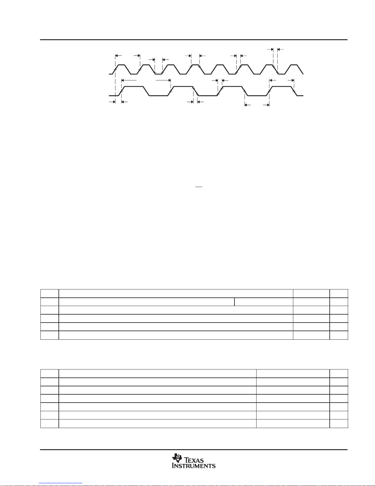
X2/CLKIN
C1
C10
C11
Electrical Specifications
C2
C3
C4
CLKOUT
C5
NOTE A: The relationship of X2/CLKIN to CLKOUT depends on the PLL bypass divide factor chosen for the CLKMD register. The waveform
relationship shown in Figure 5−3 is intended to illustrate the timing parameters based on CLKOUT = 1/2(CLKIN) configuration.
C6
C7
C8
C9
Figure 5−3. Bypass Mode Clock Timings
5.6.4 Clock Generation in Lock Mode (DPLL Synthesis Enabled)
The frequency of the reference clock provided at the X2/CLKIN pin can be multiplied by a synthesis factor of
N to generate the internal CPU clock cycle. The synthesis factor is determined by:
M
N=
D
L
where: M = the multiply factor set in the PLL_MULT field of the clock mode register
D
Valid values for M are (multiply by) 2 to 31. Valid values for D
For detailed information on clock generation configuration, see the TMS320C55x DSP Peripherals Overview
Reference Guide (literature number SPRU317).
= the divide factor set in the PLL_DIV field of the clock mode register
L
are (divide by) 1, 2, 3, and 4.
L
Table 5−5 and Table 5−6 assume testing over recommended operating conditions and H = 0.5t
c(CO)
Figure 5−4).
Table 5−5. Multiply-By-N Clock Option Timing Requirements
NO. MIN MAX UNIT
C1 t
c(CI)
C2 t
f(CI)
C3 t
r(CI)
C10 t
w(CIL)
C11 t
w(CIH)
†
The clock frequency synthesis factor and minimum X2/CLKIN cycle time should be chosen such that the resulting CLKOUT cycle time is within
the specified range (t
c(CO)
Cycle time, X2/CLKIN DPLL synthesis enabled 20
Fall time, X2/CLKIN 4 ns
Rise time, X2/CLKIN 4 ns
Pulse duration, CLKIN low 6 ns
Pulse duration, CLKIN high 6 ns
). If an external crystal is used, the X2/CLKIN cycle time is limited by the crystal frequency range listed in Table 5−2.
†
400 ns
Table 5−6. Multiply-By-N Clock Option Switching Characteristics
NO. PARAMETER MIN TYP MAX UNIT
C4 t
c(CO)
C12 t
d(CI–CO)
C6 t
f(CO)
C7 t
r(CO)
C8 t
w(COL)
C9 t
‡
N = Clock frequency synthesis factor
w(COH)
Cycle time, CLKOUT 6.94 t
Delay time, X2/CLKIN high/low to CLKOUT high/low 10 20 30 ns
Fall time, CLKOUT 1 ns
Rise time, CLKOUT 1 ns
Pulse duration, CLKOUT low H−2 H+2 ns
Pulse duration, CLKOUT high H−2 H+2 ns
c(CI)*
‡
N
1600 ns
(see
April 2001 − Revised January 2008 SPRS163H
79
Page 80

Electrical Specifications
C3
C1
X2/CLKIN
C12
C4
CLKOUT
NOTE A: The relationship of X2/CLKIN to CLKOUT depends on the PLL multiply and divide factor chosen for the CLKMD register. The waveform
relationship shown in Figure 5−3 is intended to illustrate the timing parameters based on CLKOUT = 1xCLKIN configuration.
Bypass Mode
C10
C9
C3
C11
C8
C2
C6
C7
Figure 5−4. External Multiply-by-N Clock Timings
5.6.5 Real-Time Clock Oscillator With External Crystal
The real-time clock module includes an oscillator circuit. The oscillator requires an external 32.768-kHz crystal
connected across the RTCINX1 and RTCINX2 pins. The connection of the required circuit, consisting of the
crystal and two load capacitors, is shown in Figure 5−5. The load capacitors, C
such that the equation below is satisfied. C
in the equation is the load specified for the crystal.
L
C
C
+
L
1C2
(C1) C2)
and C2, should be chosen
1
80
RTCINX1 RTCINX2
Crystal
32.768 kHz
C1 C2
Figure 5−5. Real-Time Clock Oscillator With External Crystal
NOTE: The RTC can be idled by not supplying its 32-kHz oscillator signal. In order to keep
RTC power dissipation to a minimum when the RTC module is not used, it is recommended
that the RTC module be powered up, the RTC input pin (RTCINX1) be pulled low , and the R TC
output pin (RTCINX2) be left floating.
April 2001 − Revised January 2008SPRS163H
Page 81

Electrical Specifications
5.7 Memory Interface Timings
5.7.1 Asynchronous Memory Timings
Table 5−7 and Table 5−8 assume testing over recommended operating conditions (see Figure 5−6 and
Figure 5−7).
Table 5−7. Asynchronous Memory Cycle Timing Requirements
NO. MIN MAX UNIT
M1 t
su(DV-COH)
M2 t
h(COH-DV)
M3 t
su(ARDY-COH)
M4 t
†
To ensure data setup time, simply program the strobe width wide enough. ARDY is internally synchronized. If ARDY does meet setup or hold
time, it may be recognized in the current cycle or the next cycle. Thus, ARDY can be an asynchronous input.
h(COH-ARDY)
Setup time, read data valid before CLKOUT high
Hold time, read data valid after CLKOUT high 0 ns
Setup time, ARDY valid before CLKOUT high
Hold time, ARDY valid after CLKOUT high 0 ns
Table 5−8. Asynchronous Memory Cycle Switching Characteristics
NO. PARAMETER MIN MAX UNIT
M5 t
M6 t
M7 t
M8 t
M9 t
M10 t
M11 t
M12 t
M13 t
M14 t
M15 t
M16 t
M17 t
M18 t
d(COH-CEV)
d(COH-CEIV)
d(COH-BEV)
d(COH-BEIV)
d(COH-AV)
d(COH-AIV)
d(COH-AOEV)
d(COH-AOEIV)
d(COH-AREV)
d(COH-AREIV)
d(COH-DV)
d(COH-DIV)
d(COH-AWEV)
d(COH-AWEIV)
Delay time, CLKOUT high to CEx valid 0 8 ns
Delay time, CLKOUT high to CEx invalid 0 8 ns
Delay time, CLKOUT high to BEx valid 8 ns
Delay time, CLKOUT high to BEx invalid 0 ns
Delay time, CLKOUT high to address valid 8 ns
Delay time, CLKOUT high to address invalid 0 ns
Delay time, CLKOUT high to AOE valid 0 6 ns
Delay time, CLKOUT high to AOE invalid 0 6 ns
Delay time, CLKOUT high to ARE valid 0 6 ns
Delay time, CLKOUT high to ARE invalid 0 6 ns
Delay time, CLKOUT high to data valid 6 ns
Delay time, CLKOUT high to data invalid 0 ns
Delay time, CLKOUT high to AWE valid 0 6 ns
Delay time, CLKOUT high to AWE invalid 0 6 ns
†
†
10 ns
10 ns
April 2001 − Revised January 2008 SPRS163H
81
Page 82

Electrical Specifications
CLKOUT
CEx
BEx
A[20:0]
D[15:0]
AOE
ARE
AWE
ARDY
Hold
Setup = 2 Strobe = 5 Not Ready = 2
†
M5
‡
M7
M9 M10
§
M1
M11
M13
M4
M3
M4
M3
= 1
M6
M8
Extended
Hold = 2
M2
M12
M14
†
CLKOUT is equal to CPU clock
‡
CEx
becomes active depending on the memory address space being accessed
§
A[13:0] for LQFP
Figure 5−6. Asynchronous Memory Read Timings
82
April 2001 − Revised January 2008SPRS163H
Page 83

Electrical Specifications
Extended
C
LKOUT
CEx
BEx
A[20:0]
D[15:0]
AOE
ARE
AWE
ARDY
Setup = 2 Strobe = 5 Not Ready = 2 Hold = 1
†
M5
‡
M7
M9
§
M15
M17
M3
M4
M4
M3
M18
M6
M8
M10
M16
Hold = 2
†
CLKOUT is equal to CPU clock
‡
CEx
becomes active depending on the memory address space being accessed
§
A[13:0] for LQFP
Figure 5−7. Asynchronous Memory Write Timings
April 2001 − Revised January 2008 SPRS163H
83
Page 84

Electrical Specifications
NO.
PARAMETER
UNIT
NO.
PARAMETER
UNIT
5.7.2 Synchronous DRAM (SDRAM) Timings
Table 5−9, Table 5−10, Table 5−11, and Table 5−12 assume testing over recommended operating conditions
(see Figure 5−8 through Figure 5−13).
Table 5−9. Synchronous DRAM Cycle Timing Requirements
[SDRAM Clock = 1X, (1/4)X, and (1/8)X of CPU Clock]
NO. MIN MAX UNIT
M19 t
su(DV-CLKMEMH)
M20 t
h(CLKMEMH-DV)
M21 t
c(CLKMEM)
†
The EMIFX2 bit of the External Bus Selection Register (EBSR) is cleared. See Section 3.5.1, External Bus Selection Register, for more details.
‡
Maximum SDRAM operating frequency supported is 72 MHz.
Setup time, read data valid before CLKMEM high 9 ns
Hold time, read data valid after CLKMEM high 0 ns
Cycle time, CLKMEM 13.88
†
‡
Table 5−10. Synchronous DRAM Cycle Switching Characteristics
[SDRAM Clock = 1X, (1/4)X, and (1/8)X of CPU Clock]
1X
CPU CLOCK
MIN MAX MIN MAX MIN MAX
M22 t
d(CLKMEMH-CEL)
M23 t
d(CLKMEMH-CEH)
M24 t
d(CLKMEMH-BEV)
M25 t
d(CLKMEMH-BEIV)
M26 t
d(CLKMEMH-AV)
M27 t
d(CLKMEMH-AIV)
M28 t
d(CLKMEMH-SDCASL)
M29 t
d(CLKMEMH-SDCASH)
M30 t
d(CLKMEMH-DV)
M31 t
d(CLKMEMH-DIV)
M32 t
d(CLKMEMH-SDWEL)
M33 t
d(CLKMEMH-SDWEH)
M34 t
d(CLKMEMH-SDA10V)
M35 t
d(CLKMEMH-SDA10IV)
M36 t
d(CLKMEMH-SDRASL)
M37 t
d(CLKMEMH-SDRASH)
†
The EMIFX2 bit of the External Bus Selection Register (EBSR) is cleared. See Section 3.5.1, External Bus Selection Register, for more details.
Delay time, CLKMEM high to CEx low 0 6 21 26 35 40 ns
Delay time, CLKMEM high to CEx high 0 6 21 26 35 40 ns
Delay time, CLKMEM high to BEx valid 0 6 21 26 35 40 ns
Delay time, CLKMEM high to BEx invalid 0 6 21 26 35 40 ns
Delay time, CLKMEM high to address
valid
Delay time, CLKMEM high to address
invalid
Delay time, CLKMEM high to SDCAS low 0 6 21 26 35 40 ns
Delay time, CLKMEM high to SDCAS
high
Delay time, CLKMEM high to data valid 0 6 21 26 35 40 ns
Delay time, CLKMEM high to data invalid 0 6 21 26 35 40 ns
Delay time, CLKMEM high to SDWE low 0 6 21 26 35 40 ns
Delay time, CLKMEM high to SDWE high 0 6 21 26 35 40 ns
Delay time, CLKMEM high to SDA10
valid
Delay time, CLKMEM high to SDA10
invalid
Delay time, CLKMEM high to SDRAS low 0 6 21 26 35 40 ns
Delay time, CLKMEM high to SDRAS
high
1 6 21 26 35 40 ns
1 6 21 26 35 40 ns
0 6 21 26 35 40 ns
0 6 21 26 35 40 ns
0 6 21 26 35 40 ns
0 6 21 26 35 40 ns
†
(1/4)X
CPU CLOCK
(1/8)X
CPU CLOCK
ns
84
April 2001 − Revised January 2008SPRS163H
Page 85

Electrical Specifications
Table 5−11. Synchronous DRAM Cycle Timing Requirements [SDRAM Clock = (1/2)X of CPU Clock]
NO. MIN MAX UNIT
M19 t
su(DV-CLKMEMH)
M20 t
h(CLKMEMH-DV)
M21 t
c(CLKMEM)
†
The EMIFX2 bit of the External Bus Selection Register (EBSR) is set. See Section 3.5.1, External Bus Selection Register, for more details.
‡
Maximum SDRAM operating frequency supported is 72 MHz.
Setup time, read data valid before CLKMEM high 7 ns
Hold time, read data valid after CLKMEM high 0 ns
Cycle time, CLKMEM 13.88
‡
Table 5−12. Synchronous DRAM Cycle Switching Characteristics [SDRAM Clock = (1/2)X of CPU Clock]
NO. PARAMETER MIN MAX UNIT
M22 t
d(CLKMEMH-CEL)
M23 t
d(CLKMEMH-CEH)
M24 t
d(CLKMEMH-BEV)
M25 t
d(CLKMEMH-BEIV)
M26 t
d(CLKMEMH-AV)
M27 t
d(CLKMEMH-AIV)
M28 t
d(CLKMEMH-SDCASL)
M29 t
d(CLKMEMH-SDCASH)
M30 t
d(CLKMEMH-DV)
M31 t
d(CLKMEMH-DIV)
M32 t
d(CLKMEMH-SDWEL)
M33 t
d(CLKMEMH-SDWEH)
M34 t
d(CLKMEMH-SDA10V)
M35 t
d(CLKMEMH-SDA10IV)
M36 t
d(CLKMEMH-SDRASL)
M37 t
d(CLKMEMH-SDRASH)
†
The EMIFX2 bit of the External Bus Selection Register (EBSR) is set. See Section 3.5.1, External Bus Selection Register, for more details.
Delay time, CLKMEM high to CEx low 2 10 ns
Delay time, CLKMEM high to CEx high 2 10 ns
Delay time, CLKMEM high to BEx valid 2 10 ns
Delay time, CLKMEM high to BEx invalid 2 10 ns
Delay time, CLKMEM high to address valid 2 10 ns
Delay time, CLKMEM high to address invalid 2 10 ns
Delay time, CLKMEM high to SDCAS low 2 10 ns
Delay time, CLKMEM high to SDCAS high 2 10 ns
Delay time, CLKMEM high to data valid 2 10 ns
Delay time, CLKMEM high to data invalid 2 10 ns
Delay time, CLKMEM high to SDWE low 2 10 ns
Delay time, CLKMEM high to SDWE high 2 10 ns
Delay time, CLKMEM high to SDA10 valid 2 10 ns
Delay time, CLKMEM high to SDA10 invalid 2 10 ns
Delay time, CLKMEM high to SDRAS low 2 10 ns
Delay time, CLKMEM high to SDRAS high 2 10 ns
†
ns
†
April 2001 − Revised January 2008 SPRS163H
85
Page 86

Electrical Specifications
CLKMEM
READ READ READ
M21
M22
M27
†
CEx
M24
‡
BEx
M26
EMIF.A[13:0]
D[15:0]
SDA10
SDRAS
SDCAS
SDWE
†
The chip enable that becomes active depends on the address being accessed.
‡
All BE[1:0]
active until the next access that is not an SDRAM read occurs.
signals are driven low (active) during reads. Byte manipulation of the read data is performed inside the EMIF. These signals remain
CA1 CA2 CA3
M34
M28
M23
M19
M20
D1 D2 D3
M35
M29
86
Figure 5−8. Three SDRAM Read Commands
April 2001 − Revised January 2008SPRS163H
Page 87

CLKMEM
Electrical Specifications
WRITE WRITE WRITE
CEx
BEx
EMIF.A[13:0]
D[15:0]
SDA10
SDRAS
SDCAS
M22
†
M25
M24
‡
BE1 BE2 BE3
M27
M26
CA1 CA2 CA3
M31
M30
D1 D2 D3
M34
M28
M23
M35
M29
M32
SDWE
†
The chip enable that becomes active depends on the address being accessed.
‡
All BE[1:0]
active until the next access that is not an SDRAM read occurs.
signals are driven low (active) during reads. Byte manipulation of the read data is performed inside the EMIF. These signals remain
Figure 5−9. Three SDRAM WRT Commands
M33
April 2001 − Revised January 2008 SPRS163H
87
Page 88

Electrical Specifications
CLKMEM
ACTV
M22
†
CEx
‡
BEx
M26
EMIF.A[13:0]
D[15:0]
M34
SDA10
M36
SDRAS
SDCAS
SDWE
†
The chip enable that becomes active depends on the address being accessed.
‡
All BE[1:0] signals are driven low (active) during reads. Byte manipulation of the read data is performed inside the EMIF. These signals remain
active until the next access that is not an SDRAM read occurs.
Bank Activate/Row Address
M23
M37
88
Figure 5−10. SDRAM ACTV Command
April 2001 − Revised January 2008SPRS163H
Page 89

CLKMEM
Electrical Specifications
DCAB
CEx
BEx
EMIF.A[13:0]
D[15:0]
SDA10
SDRAS
M22
†
‡
M34
M36
M23
M35
M37
SDCAS
M32
SDWE
†
The chip enable that becomes active depends on the address being accessed.
‡
All BE[1:0]
active until the next access that is not an SDRAM read occurs.
signals are driven low (active) during reads. Byte manipulation of the read data is performed inside the EMIF. These signals remain
Figure 5−11. SDRAM DCAB Command
M33
April 2001 − Revised January 2008 SPRS163H
89
Page 90

Electrical Specifications
CLKMEM
REFR
CEx
BEx
EMIF.A[13:0]
D[15:0]
SDA10
SDRAS
M22
†
‡
M36
M28
M23
M37
M29
SDCAS
SDWE
†
The chip enable that becomes active depends on the address being accessed.
‡
All BE[1:0]
remain active until the next access that is not an SDRAM read occurs.
signals are driven low (active) during reads. Byte manipulation of the read data is performed inside the EMIF. These signals
Figure 5−12. SDRAM REFR Command
90
April 2001 − Revised January 2008SPRS163H
Page 91

CLKMEM
Electrical Specifications
MRS
CEx
BEx
EMIF.A[13:0]
D[15:0]
SDA10
SDRAS
M22
†
‡
M26
MRS Value 0x30
M36
M28
M23
M27
§
M37
M29
SDCAS
M32
SDWE
†
The chip enable that becomes active depends on the address being accessed.
‡
All BE[1:0]
active until the next access that is not an SDRAM read occurs.
§
Write burst length = 1
Read latency = 3
Burst type = 0 (serial)
Burst length = 1
signals are driven low (active) during reads. Byte manipulation of the read data is performed inside the EMIF. These signals remain
Figure 5−13. SDRAM MRS Command
M33
April 2001 − Revised January 2008 SPRS163H
91
Page 92

Electrical Specifications
5.8 Reset Timings
5.8.1 Power-Up Reset (On-Chip Oscillator Active)
Table 5−13 assumes testing over recommended operating conditions (see Figure 5−14).
Table 5−13. Power-Up Reset (On-Chip Oscillator Active) Timing Requirements
NO. MIN MAX UNIT
R1 t
†
‡
CLKOUT
h(SUPSTBL-RSTL)
Oscillator stable time depends on the crystal characteristic (i.e., frequency, ESR, etc.) which varies from one crystal manufacturer to another.
Based on the crystal characteristics, the oscillator stable time can be in the range of a few to 10s of ms. A reset circuit with 100 ms or more delay
time will ensure the oscillator stabilized before the RESET
P = 1/(input clock frequency) in ns. For example, when input clock is 12 MHz, P = 83.33 ns.
CV
DD
DV
DD
RESET
Hold time, RESET low after oscillator stable
goes high.
†
R1
3P
‡
ns
Figure 5−14. Power-Up Reset (On-Chip Oscillator Active) Timings
5.8.2 Power-Up Reset (On-Chip Oscillator Inactive)
Table 5−14 and Table 5−15 assume testing over recommended operating conditions (see Figure 5−15).
Table 5−14. Power-Up Reset (On-Chip Oscillator Inactive) Timing Requirements
NO. MIN MAX UNIT
R2 t
‡
h(CLKOUTV-RSTL)
P = 1/(input clock frequency) in ns. For example, when input clock is 12 MHz, P = 83.33 ns.
Hold time, CLKOUT valid to RESET low 3P
Table 5−15. Power-Up Reset (On-Chip Oscillator Inactive) Switching Characteristics
NO. PARAMETER MIN MAX UNIT
R3 t
X2/CLKIN
CLKOUT
CV
DD
DV
DD
d(CLKINV-CLKOUTV)
Delay time, CLKIN valid to CLKOUT valid 30 ns
R3
R2
‡
ns
RESET
Figure 5−15. Power-Up Reset (On-Chip Oscillator Inactive) Timings
92
April 2001 − Revised January 2008SPRS163H
Page 93

Electrical Specifications
H
,
5.8.3 Warm Reset
Table 5−16 and Table 5−17 assume testing over recommended operating conditions (see Figure 5−16).
Table 5−16. Reset Timing Requirements
NO. MIN MAX UNIT
R4 t
w(RSL)
†
P = 1/CPU clock frequency in ns. For example, when running parts at 144 MHz, use P = 6.94 ns.
Pulse width, reset low 3P
†
ns
Table 5−17. Reset Switching Characteristics
NO. PARAMETER MIN MAX UNIT
R5 t
d(RSTH-BKV)
R6 t
d(RSTH-HIGHV)
R7 t
d(RSTL-ZIV)
R8 t
d(RSTH-ZV)
†
P = 1/CPU clock frequency in ns. For example, when running parts at 144 MHz, use P = 6.94 ns.
‡
BK group: Pins with bus keepers, holds previous state during reset. Following low-to-high transition of RESET
logic state.
BK group pins: A’[0], A[15:0], D[15:0], C[14:2], C0, GPIO5, S13, and S23
§
High group: Following low-to-high transition of RESET
High group pins: C1[HPI.HINT], XF
¶
Z group: Bidirectional pins which become input or output pins. Following low-to-high transition of RESET
Z group pins: C1[EMIF.AOE], GPIO[7:6, 4:0], TIN/TOUT0, SDA, SCL, CLKR0, FSRX0, CLKX0, DX0, FSX0, S[25:24, 22:20, 15:14, 12:10],
A[20:16]
RESET
BK Group
igh Group
Z Group
†
‡
§
Delay time, reset high to BK group valid
Delay time, reset high to High group valid
Delay time, reset low to Z group invalid
Delay time, reset high to Z group valid
, these pins go to logic-high state.
R7
‡
§
¶
¶
†
38P + 6 ns
38P + 6 ns
20 ns
38P + 6 ns
, these pins go to their post-reset
, these pins go to high-impedance state.
R5
R6
R8
†
BK group pins: A’[0], A[15:0], D[15:0], C[14:2], C0, GPIO5, S13, and S23
‡
High group pins: C1[HPI.HINT], XF
§
Z group pins: C1[EMIF.AOE], GPIO[7:6, 4:0], TIN/TOUT0, SDA, SCL, CLKR0, FSRX0, CLKX0, DX0, FSX0, S[25:24, 22:20, 15:14, 12:10]
A[20:16]
April 2001 − Revised January 2008 SPRS163H
Figure 5−16. Reset Timings
93
Page 94

Electrical Specifications
5.9 External Interrupt Timings
Table 5−18 assumes testing over recommended operating conditions (see Figure 5−17).
Table 5−18. External Interrupt Timing Requirements
NO. MIN MAX UNIT
I1 t
w(INTL)A
I2 t
w(INTH)A
†
P = 1/CPU clock frequency in ns. For example, when running parts at 144 MHz, use P = 6.94 ns.
INTn
Pulse width, interrupt low, CPU active 3P ns
Pulse width, interrupt high, CPU active 2P ns
I1
I2
†
Figure 5−17. External Interrupt Timings
5.10 Wake-Up From IDLE
Table 5−19 assumes testing over recommended operating conditions (see Figure 5−18).
Table 5−19. Wake-Up From IDLE Switching Characteristics
NO. PARAMETER MIN TYP MAX UNIT
ID1 t
d(WKPEVTL-CLKGEN)
ID2 t
h(CLKGEN-WKPEVTL)
ID3 t
w(WKPEVTL)
†
P = 1/CPU clock frequency in ns. For example, when running parts at 144 MHz, use P = 6.94 ns.
‡
Based on 12-MHz crystal used with on-chip oscillator at 25°C. This number will vary based on the actual crystal characteristics operating condition
and the PC board layout and the parasitics.
§
Following the clock generation domain idle, the INTx
the CPU wake-up. Holding the INTx
sent to the CPU depends on the INTx
Delay time, wake-up event low to clock generation enable
(CPU and clock domain idle)
Hold time, clock generation enable to wake-up event low
(CPU and clock domain in idle)
Pulse width, wake-up event low (for CPU idle only) 3P ns
becomes level-sensitive and stays that way until the low-to-high transition of INTx following
low longer than minimum requirement will send more than one interrupt to the CPU. The number of interrupts
-low time following the CPU wake-up from IDLE.
†
‡
3P
1.25
§
ms
ns
X1
RESET
,
INTx
Figure 5−18. Wake-Up From IDLE Timings
94
ID1
ID2
ID3
April 2001 − Revised January 2008SPRS163H
Page 95

Electrical Specifications
5.11 XF Timings
Table 5−20 assumes testing over recommended operating conditions (see Figure 5−19).
Table 5−20. XF Switching Characteristics
NO. PARAMETER MIN MAX UNIT
X1 t
d(XF)
Delay time, CLKOUT high to XF high 0 3
Delay time, CLKOUT high to XF low 0 3
ns
CLKOUT
†
CLKOUT reflects the CPU clock.
†
XF
X1
Figure 5−19. XF Timings
April 2001 − Revised January 2008 SPRS163H
95
Page 96

Electrical Specifications
su(GPIO-COH)
G1
t
su(GPIO-COH)
Setup time, IOx input valid before CLKOUT high
ns
h(COH-GPIO)
d(COH-GPIO)
5.12 General-Purpose Input/Output (GPIOx) Timings
Table 5−21 and Table 5−22 assume testing over recommended operating conditions (see Figure 5−20).
Table 5−21. GPIO Pins Configured as Inputs Timing Requirements
NO. MIN MAX UNIT
GPIO 6
†
G1 t
G2 t
h(COH-GPIO)
†
AGPIO pins: A[15:0]
‡
EHPIGPIO pins: C13, C10, C7, C5, C4, and C0
Setup time, IOx input valid before CLKOUT high
Hold time, IOx input valid after CLKOUT high
AGPIO
EHPIGPIO
GPIO 0
AGPIO
EHPIGPIO
‡
†
‡
Table 5−22. GPIO Pins Configured as Outputs Switching Characteristics
NO. PARAMETER MIN MAX UNIT
GPIO 0 5
G3 t
d(COH-GPIO)
†
AGPIO pins: A[15:0]
‡
EHPIGPIO pins: C13, C10, C7, C5, C4, and C0
Delay time, CLKOUT high to IOx output change
†
AGPIO
EHPIGPIO
‡
8
8
0
0
1 9
1 9
ns
ns
ns
CLKOUT
Input Mode
Output Mode
†
CLKOUT reflects the CPU clock.
†
IOx
IOx
Figure 5−20. General-Purpose Input/Output (IOx) Signal Timings
G1
G2
G3
96
April 2001 − Revised January 2008SPRS163H
Page 97

5.13 TIN/TOUT Timings (Timer0 Only)
Table 5−23 and Table 5−24 assume testing over recommended operating conditions (see Figure 5−21 and
Figure 5−22).
Electrical Specifications
Table 5−23. TIN/TOUT Pins Configured as Inputs Timing Requirements
NO. MIN MAX UNIT
T4 t
w(TIN/TOUTL)
T5 t
w(TIN/TOUTH)
†
P = 1/CPU clock frequency. For example, when running parts at 144 MHz, use P = 6.94 ns.
‡
Only the Timer0 signal is externally available. The Timer1 signal is internally terminated and is not available for external use.
Pulse width, TIN/TOUT low 2P + 1 ns
Pulse width, TIN/TOUT high 2P + 1 ns
Table 5−24. TIN/TOUT Pins Configured as Outputs Switching Characteristics
NO. PARAMETER MIN MAX UNIT
T1 t
d(COH-TIN/TOUTH)
T2 t
d(COH-TIN/TOUTL)
T3 t
w(TIN/TOUT)
†
P = 1/CPU clock frequency. For example, when running parts at 144 MHz, use P = 6.94 ns.
‡
Only the Timer0 signal is externally available. The Timer1 signal is internally terminated and is not available for external use.
§
For proper operation of the TIN/TOUT pin configured as an output, the timer period must be configured for at least 4 cycles.
TIN/TOUT
as Input
Delay time, CLKOUT high to TIN/TOUT high 0 3 ns
Delay time, CLKOUT high to TIN/TOUT low 0 3 ns
Pulse duration, TIN/TOUT (output) P − 1 ns
T5
T4
†‡
†‡§
CLKOUT
TIN/TOUT
as Output
Figure 5−21. TIN/TOUT Timings When Configured as Inputs
T1
T2
T3
Figure 5−22. TIN/TOUT Timings When Configured as Outputs
April 2001 − Revised January 2008 SPRS163H
97
Page 98

Electrical Specifications
5.14 Multichannel Buffered Serial Port (McBSP) Timings
5.14.1 McBSP Transmit and Receive Timings
Table 5−25 and Table 5−26 assume testing over recommended operating conditions (see Figure 5−23 and
Figure 5−24).
Table 5−25. McBSP T
NO. MIN MAX UNIT
MC1 t
c(CKRX)
MC2 t
w(CKRX)
MC3 t
r(CKRX)
MC4 t
f(CKRX)
MC5 t
su(FRH-CKRL)
MC6 t
h(CKRL-FRH)
MC7 t
su(DRV-CKRL)
MC8 t
h(CKRL-DRV)
MC9 t
su(FXH-CKXL)
MC10 t
†
‡
h(CKXL-FXH)
Polarity bits CLKRP = CLKXP = FSRP = FSXP = 0. If the polarity of any of the signals is inverted, then the timing references of
also inverted.
P = 1/CPU clock frequency. For example, when running parts at 144 MHz, use P = 6.94 ns. In addition to CPU frequency, the maximum operating
frequency of the serial port also depends on meeting the rest of the switching characteristics and timing requirements parameters specified.
Cycle time, CLKR/X CLKR/X ext 2P
Pulse duration, CLKR/X high or CLKR/X low CLKR/X ext P–1
Rise time, CLKR/X CLKR/X ext 6 ns
Fall time, CLKR/X CLKR/X ext 6 ns
Setup time, external FSR high before CLKR low
Hold time, external FSR high after CLKR low
Setup time, DR valid before CLKR low
Hold time, DR valid after CLKR low
Setup time, external FSX high before CLKX low
Hold time, external FSX high after CLKX low
ransmit and Receive Timing Requirements
CLKR int 12
CLKR ext
CLKR int 3
CLKR ext
CLKR int 10
CLKR ext
CLKR int 3
CLKR ext
CLKX int 12
CLKX ext
CLKX int 4
CLKX ext 2
†
‡
‡
2
2
2
3
2
that signal are
ns
ns
ns
ns
ns
ns
ns
ns
98
April 2001 − Revised January 2008SPRS163H
Page 99

Electrical Specifications
Disable time, DX high-impedance from CLKX high
Disable time, DX high-impedance from CLKX high
Delay time, CLKX high to DX valid.
Delay time, CLKX high to DX valid.
MC16
t
DXENA = 0
ns
when in Data Delay 1 or 2
DXENA = 1
¶
high
¶
DXENA = 0
MC17
t
ns
when in Data Delay 1 or 2
DXENA = 1
DXENA = 0
MC18
t
ns
when in Data Delay 0 (XDATDLY=00b)
DXENA = 1
DXENA = 0
MC19
t
ns
when in Data Delay 0 (XDATDLY=00b)
DXENA = 1
Table 5−26. McBSP Transmit and Receive Switching Characteristics
NO. PARAMETER MIN MAX UNIT
MC1 t
MC11 t
MC12 t
MC13 t
MC14 t
MC15 t
†
Polarity bits CLKRP = CLKXP = FSRP = FSXP = 0. If the polarity of any of the signals is inverted, then the timing references of
also inverted.
‡
P = 1/CPU clock frequency. For example, when running parts at 144 MHz, use P = 6.94 ns. In addition to CPU frequency, the maximum operating
frequency of the serial port also depends on meeting the rest of the switching characteristics and timing requirements parameters specified.
§
T = CLKRX period = (1 + CLKGDV) * P
C = CLKRX low pulse width = T/2 when CLKGDV is odd or zero and = (CLKGDV/2) * P when CLKGDV is even
D = CLKRX high pulse width = T/2 when CLKGDV is odd or zero and = (CLKGDV/2 + 1) * P when CLKGDV is even
¶
See the TMS320C55x DSP Peripherals Overview Reference Guide (literature number SPRU317) for a description of the DX enable (DXENA)
and data delay features of the McBSP.
c(CKRX)
w(CKRXH)
w(CKRXL)
d(CKRH-FRV)
d(CKXH-FXV)
dis(CKXH-DXHZ)
d(CKXH-DXV)
en(CKXH-DX)
d(FXH-DXV)
en(FXH-DX)
Cycle time, CLKR/X CLKR/X int 2P ns
Pulse duration, CLKR/X high CLKR/X int D−1
Pulse duration, CLKR/X low CLKR/X int C−1
Delay time, CLKR high to internal FSR valid
Delay time, CLKX high to internal FSX valid
following last data bit
This applies to all bits except the first bit transmitted.
Delay time, CLKX high to DX valid
Only applies to first bit transmitted
(XDATDLY=01b or 10b) modes
Enable time, DX driven from CLKX
Only applies to first bit transmitted
(XDATDLY=01b or 10b) modes
Delay time, FSX high to DX valid
Only applies to first bit transmitted
mode.
Enable time, DX driven from FSX high
Only applies to first bit transmitted
mode
¶
¶
¶
CLKR int −4 1
CLKR ext
CLKX int −4 1
CLKX ext
CLKX int 0 2
CLKX ext
CLKX int 6
CLKX ext 16
CLKX int 6
CLKX ext 16
CLKX int 2P + 6
CLKX ext 2P + 16
CLKX int 2
CLKX ext 4
CLKX int 2P − 2
CLKX ext 2P
FSX int 6
FSX ext 16
FSX int 2P + 6
FSX ext 2P + 16
FSX int 0
FSX ext 3
FSX int 2P − 2
FSX ext 2P − 2
†‡
§
§
4 13
4 14
3 11
D+1§ns
C+1§ns
that signal are
ns
ns
ns
April 2001 − Revised January 2008 SPRS163H
99
Page 100

Electrical Specifications
CLKR
MC1
MC2, MC11
MC2, MC12
MC3
FSR (Int)
FSR (Ext)
DR
(RDATDLY=00b)
DR
(RDATDLY=01b)
DR
(RDATDLY=10b)
CLKX
MC13
MC5
MC7
Bit (n−1) (n−2) (n−3) (n−4)
MC6
MC8
MC7
Bit (n−1) (n−2) (n−3)
Figure 5−23. McBSP Receive Timings
MC1
MC2, MC11
MC2, MC12
MC13
MC7
MC8
Bit (n−1) (n−2)
MC3
MC4
MC8
MC4
MC14 MC14
FSX (Int)
MC9
FSX (Ext)
MC19
(XDATDLY=00b)
DX
DX
(XDATDLY=01b)
DX
(XDATDLY=10b)
Bit 0 Bit (n−1) (n−2) (n−3) (n−4)
Bit 0
MC15
Bit 0
Figure 5−24. McBSP Transmit Timings
100
MC18
MC17
MC10
MC16
MC16
Bit (n−1) (n−2) (n−3)
MC16
MC17
Bit (n−1) (n−2)
April 2001 − Revised January 2008SPRS163H
 Loading...