

Page 1

TMS320C6472/TMS320TCI6486 DSP
Ethernet Media Access Controller (EMAC)/
Management Data Input/Output (MDIO) Module
User's Guide
Literature Number: SPRUEF8F
March 2006–Revised November 2010
Page 2

2
SPRUEF8F–March 2006–Revised November 2010
Submit Documentation Feedback
Copyright © 2006–2010, Texas Instruments Incorporated
Page 3

Preface ...................................................................................................................................... 10
1 Introduction ...................................................................................................................... 11
1.1 Purpose of the Peripheral ............................................................................................. 11
1.2 Features ................................................................................................................. 11
1.3 Functional Block Diagram ............................................................................................. 12
1.4 Industry Standard(s) Compliance Statement ....................................................................... 14
2 EMAC Functional Architecture ............................................................................................ 15
2.1 Clock Control ........................................................................................................... 15
2.2 Memory Map ............................................................................................................ 16
2.3 System-Level Connections ........................................................................................... 17
2.4 Ethernet Protocol Overview .......................................................................................... 29
2.5 Programming Interface ................................................................................................ 31
2.6 Communications Port Programming Interface (CPPI) ............................................................ 40
2.7 Ethernet Multicore Interrupt Combiner (EMIC) Module ........................................................... 40
2.8 Management Data Input/Output (MDIO) Module .................................................................. 47
2.9 EMAC Module .......................................................................................................... 52
2.10 Media Independent Interfaces ........................................................................................ 54
2.11 Packet Receive Operation ............................................................................................ 58
2.12 Packet Transmit Operation ........................................................................................... 62
2.13 Receive and Transmit Latency ....................................................................................... 63
2.14 Transfer Node Priority ................................................................................................. 63
2.15 Reset Considerations .................................................................................................. 64
2.16 Initialization ............................................................................................................. 65
2.17 Interrupt Support ....................................................................................................... 67
2.18 Power Management ................................................................................................... 69
2.19 Emulation Considerations ............................................................................................. 69
3 EMIC Module Registers ...................................................................................................... 71
3.1 EW_INTCTL Registers ................................................................................................ 71
3.2 RPIC Registers ......................................................................................................... 71
3.3 TPIC Registers ......................................................................................................... 74
3.4 Prescalar Configuration Register (PSCFG) ........................................................................ 75
4 MDIO Registers ................................................................................................................. 76
4.1 Introduction ............................................................................................................. 76
4.2 MDIO Version Register (VERSION) ................................................................................. 77
4.3 MDIO Control Register (CONTROL) ................................................................................ 78
4.4 PHY Acknowledge Status Register (ALIVE) ....................................................................... 79
4.5 PHY Link Status Register (LINK) .................................................................................... 80
4.6 MDIO Link Status Change Interrupt (Unmasked) Register (LINKINTRAW) ................................... 81
4.7 MDIO Link Status Change Interrupt (Masked) Register (LINKINTMASKED) .................................. 82
4.8 MDIO User Command Complete Interrupt (Unmasked) Register (USERINTRAW) .......................... 83
4.9 MDIO User Command Complete Interrupt (Masked) Register (USERINTMASKED) ......................... 84
4.10 MDIO User Command Complete Interrupt Mask Set Register (USERINTMASKSET) ....................... 85
SPRUEF8F–March 2006–Revised November 2010 Table of Contents
Submit Documentation Feedback
Copyright © 2006–2010, Texas Instruments Incorporated
3
Page 4

www.ti.com
4.11 MDIO User Command Complete Interrupt Mask Clear Register (USERINTMASKCLEAR) ................. 86
4.12 MDIO User Access Register 0 (USERACCESS0) ................................................................ 87
4.13 MDIO User PHY Select Register 0 (USERPHYSEL0) ............................................................ 88
4.14 MDIO User Access Register 1 (USERACCESS1) ................................................................ 89
4.15 MDIO User PHY Select Register 1 (USERPHYSEL1) ............................................................ 90
5 EMAC Port Registers ......................................................................................................... 91
5.1 Transmit Identification and Version Register (TXIDVER) ........................................................ 95
5.2 Transmit Control Register (TXCONTROL) ......................................................................... 96
5.3 Transmit Teardown Register (TXTEARDOWN) ................................................................... 97
5.4 Receive Identification and Version Register (RXIDVER) ......................................................... 98
5.5 Receive Control Register (RXCONTROL) .......................................................................... 99
5.6 Receive Teardown Register (RXTEARDOWN) .................................................................. 100
5.7 Transmit Interrupt Status (Unmasked) Register (TXINTSTATRAW) .......................................... 101
5.8 Transmit Interrupt Status (Masked) Register (TXINTSTATMASKED) ........................................ 102
5.9 Transmit Interrupt Mask Set Register (TXINTMASKSET) ...................................................... 103
5.10 Transmit Interrupt Mask Clear Register (TXINTMASKCLEAR) ................................................ 104
5.11 MAC Input Vector Register (MACINVECTOR) ................................................................... 105
5.12 MAC End-of-Interrupt Vector Register (MACEOIVECTOR) .................................................... 106
5.13 Receive Interrupt Status (Unmasked) Register (RXINTSTATRAW) ........................................... 107
5.14 Receive Interrupt Status (Masked) Register (RXINTSTATMASKED) ......................................... 108
5.15 Receive Interrupt Mask Set Register (RXINTMASKSET) ....................................................... 109
5.16 Receive Interrupt Mask Clear Register (RXINTMASKCLEAR) ................................................. 110
5.17 MAC Interrupt Status (Unmasked) Register (MACINTSTATRAW) ............................................ 111
5.18 MAC Interrupt Status (Masked) Register (MACINTSTATMASKED) .......................................... 112
5.19 MAC Interrupt Mask Set Register (MACINTMASKSET) ........................................................ 113
5.20 MAC Interrupt Mask Clear Register (MACINTMASKCLEAR) .................................................. 114
5.21 Receive Multicast/Broadcast/Promiscuous Channel Enable Register (RXMBPENABLE) .................. 115
5.22 Receive Unicast Enable Set Register (RXUNICASTSET) ...................................................... 118
5.23 Receive Unicast Clear Register (RXUNICASTCLEAR) ......................................................... 119
5.24 Receive Maximum Length Register (RXMAXLEN) .............................................................. 120
5.25 Receive Buffer Offset Register (RXBUFFEROFFSET) ......................................................... 121
5.26 Receive Filter Low Priority Frame Threshold Register (RXFILTERLOWTHRESH) ......................... 122
5.27 Receive Channel 0-7 Flow Control Threshold Register (RXnFLOWTHRESH) .............................. 123
5.28 Receive Channel 0-7 Free Buffer Count Register (RXnFREEBUFFER) ..................................... 124
5.29 MAC Control Register (MACCONTROL) .......................................................................... 125
5.30 MAC Status Register (MACSTATUS) ............................................................................. 127
5.31 Emulation Control Register (EMCONTROL) ...................................................................... 129
5.32 FIFO Control Register (FIFOCONTROL) ......................................................................... 130
5.33 MAC Configuration Register (MACCONFIG) ..................................................................... 131
5.34 Soft Reset Register (SOFTRESET) ................................................................................ 132
5.35 MAC Source Address Low Bytes Register (MACSRCADDRLO) .............................................. 133
5.36 MAC Source Address High Bytes Register (MACSRCADDRHI) .............................................. 134
5.37 MAC Hash Address Register 1 (MACHASH1) ................................................................... 135
5.38 MAC Hash Address Register 2 (MACHASH2) ................................................................... 136
5.39 Back Off Test Register (BOFFTEST) .............................................................................. 137
5.40 Transmit Pacing Algorithm Test Register (TPACETEST) ....................................................... 138
5.41 Receive Pause Timer Register (RXPAUSE) ...................................................................... 139
5.42 Transmit Pause Timer Register (TXPAUSE) ..................................................................... 140
4
Contents SPRUEF8F–March 2006–Revised November 2010
Copyright © 2006–2010, Texas Instruments Incorporated
Submit Documentation Feedback
Page 5

www.ti.com
5.43 MAC Address Low Bytes Register (MACADDRLO) ............................................................. 141
5.44 MAC Address High Bytes Register (MACADDRHI) ............................................................. 142
5.45 MAC Index Register (MACINDEX) ................................................................................. 143
5.46 Transmit Channel 0-7 DMA Head Descriptor Pointer Register (TXnHDP) ................................... 144
5.47 Receive Channel 0-7 DMA Head Descriptor Pointer Register (RXnHDP) .................................... 145
5.48 Transmit Channel 0-7 Completion Pointer Register (TXnCP) .................................................. 146
5.49 Receive Channel 0-7 Completion Pointer Register (RXnCP) .................................................. 147
5.50 Network Statistics Registers ........................................................................................ 148
Appendix A Glossary ............................................................................................................... 157
Appendix B Revision History ..................................................................................................... 159
SPRUEF8F–March 2006–Revised November 2010 Contents
Submit Documentation Feedback
Copyright © 2006–2010, Texas Instruments Incorporated
5
Page 6

www.ti.com
List of Figures
1 EMAC and MDIO Block Diagram........................................................................................ 12
2 Ethernet Configuration with MII Interface .............................................................................. 18
3 Ethernet Configuration with RMII Interface ............................................................................ 20
4 Ethernet Configuration with GMII Interface ............................................................................ 21
5 Ethernet Configuration with RGMII Interface .......................................................................... 23
6 Ethernet Configuration with S3MII Interface ........................................................................... 25
7 S3MII Multi-PHY Configuration .......................................................................................... 27
8 S3MII Switch Configuration .............................................................................................. 28
9 Ethernet Frame............................................................................................................ 29
10 Basic Descriptor Format.................................................................................................. 31
11 Typical Descriptor Linked List............................................................................................ 32
12 Transmit Descriptor Format .............................................................................................. 34
13 Receive Descriptor Format............................................................................................... 37
14 EMIC Block Diagram...................................................................................................... 41
15 Pacing Block ............................................................................................................... 42
16 TDSM State Transition Diagram......................................................................................... 43
17 DSM State Transition Diagram .......................................................................................... 44
18 Transmit Pacer and Interrupt Combiner................................................................................ 45
19 Receive Pacer and Interrupt Combiner................................................................................. 46
20 Common Interrupt Combiner............................................................................................. 47
21 MDIO Module Block Diagram............................................................................................ 48
22 EMAC Module Block Diagram........................................................................................... 52
23 EW_INTCTL Register..................................................................................................... 71
24 RPCFG Register........................................................................................................... 72
25 RPSTAT Register ......................................................................................................... 73
26 TPCFG Register........................................................................................................... 74
27 TPSTAT Register.......................................................................................................... 75
28 Prescalar Configuration Register (PSCFG)............................................................................ 75
29 MDIO Version Register (VERSION) .................................................................................... 77
30 MDIO Control Register (CONTROL).................................................................................... 78
31 PHY Acknowledge Status Register (ALIVE)........................................................................... 79
32 PHY Link Status Register (LINK)........................................................................................ 80
33 MDIO Link Status Change Interrupt (Unmasked) Register (LINKINTRAW)....................................... 81
34 MDIO Link Status Change Interrupt (Masked) Register (LINKINTMASKED) ..................................... 82
35 MDIO User Command Complete Interrupt (Unmasked) Register (USERINTRAW).............................. 83
36 MDIO User Command Complete Interrupt (Masked) Register (USERINTMASKED) ............................ 84
37 MDIO User Command Complete Interrupt Mask Set Register (USERINTMASKSET)........................... 85
38 MDIO User Command Complete Interrupt Mask Clear Register (USERINTMASKCLEAR) .................... 86
39 MDIO User Access Register 0 (USERACCESS0) .................................................................... 87
40 MDIO User PHY Select Register 0 (USERPHYSEL0) ............................................................... 88
41 MDIO User Access Register 1 (USERACCESS1) .................................................................... 89
42 MDIO User PHY Select Register 1 (USERPHYSEL1) ............................................................... 90
43 Transmit Identification and Version Register (TXIDVER) ............................................................ 95
44 Transmit Control Register (TXCONTROL)............................................................................. 96
45 Transmit Teardown Register (TXTEARDOWN)....................................................................... 97
46 Receive Identification and Version Register (RXIDVER)............................................................. 98
47 Receive Control Register (RXCONTROL) ............................................................................. 99
6
List of Figures SPRUEF8F–March 2006–Revised November 2010
Copyright © 2006–2010, Texas Instruments Incorporated
Submit Documentation Feedback
Page 7

www.ti.com
48 Receive Teardown Register (RXTEARDOWN)...................................................................... 100
49 Transmit Interrupt Status (Unmasked) Register (TXINTSTATRAW).............................................. 101
50 Transmit Interrupt Status (Masked) Register (TXINTSTATMASKED) ............................................ 102
51 Transmit Interrupt Mask Set Register (TXINTMASKSET).......................................................... 103
52 Transmit Interrupt Mask Clear Register (TXINTMASKCLEAR).................................................... 104
53 MAC Input Vector Register (MACINVECTOR)....................................................................... 105
54 MAC End-of-Interrupt Vector Register (MACEOIVECTOR)........................................................ 106
55 Receive Interrupt Status (Unmasked) Register (RXINTSTATRAW) .............................................. 107
56 Receive Interrupt Status (Masked) Register (RXINTSTATMASKED)............................................. 108
57 Receive Interrupt Mask Set Register (RXINTMASKSET) .......................................................... 109
58 Receive Interrupt Mask Clear Register (RXINTMASKCLEAR) .................................................... 110
59 MAC Interrupt Status (Unmasked) Register (MACINTSTATRAW)................................................ 111
60 MAC Interrupt Status (Masked) Register (MACINTSTATMASKED) .............................................. 112
61 MAC Interrupt Mask Set Register (MACINTMASKSET)............................................................ 113
62 MAC Interrupt Mask Clear Register (MACINTMASKCLEAR)...................................................... 114
63 Receive Multicast/Broadcast/Promiscuous Channel Enable Register (RXMBPENABLE) ..................... 115
64 Receive Unicast Enable Set Register (RXUNICASTSET).......................................................... 118
65 Receive Unicast Clear Register (RXUNICASTCLEAR)............................................................. 119
66 Receive Maximum Length Register (RXMAXLEN).................................................................. 120
67 Receive Buffer Offset Register (RXBUFFEROFFSET)............................................................. 121
68 Receive Filter Low Priority Frame Threshold Register (RXFILTERLOWTHRESH)............................. 122
69 Receive Channel n Flow Control Threshold Register (RXnFLOWTHRESH).................................... 123
70 Receive Channel n Free Buffer Count Register (RXnFREEBUFFER) ........................................... 124
71 MAC Control Register (MACCONTROL) ............................................................................. 125
72 MAC Status Register (MACSTATUS)................................................................................. 127
73 Emulation Control Register (EMCONTROL) ......................................................................... 129
74 FIFO Control Register (FIFOCONTROL)............................................................................. 130
75 MAC Configuration Register (MACCONFIG)......................................................................... 131
76 Soft Reset Register (SOFTRESET)................................................................................... 132
77 MAC Source Address Low Bytes Register (MACSRCADDRLO).................................................. 133
78 MAC Source Address High Bytes Register (MACSRCADDRHI) .................................................. 134
79 MAC Hash Address Register 1 (MACHASH1)....................................................................... 135
80 MAC Hash Address Register 2 (MACHASH2)....................................................................... 136
81 Back Off Test Register (BOFFTEST) ................................................................................. 137
82 Transmit Pacing Algorithm Test Register (TPACETEST) .......................................................... 138
83 Receive Pause Timer Register (RXPAUSE) ......................................................................... 139
84 Transmit Pause Timer Register (TXPAUSE)......................................................................... 140
85 MAC Address Low Bytes Register (MACADDRLO)................................................................. 141
86 MAC Address High Bytes Register (MACADDRHI) ................................................................. 142
87 MAC Index Register (MACINDEX) .................................................................................... 143
88 Transmit Channel n DMA Head Descriptor Pointer Register (TXnHDP) ......................................... 144
89 Receive Channel n DMA Head Descriptor Pointer Register (RXnHDP).......................................... 145
90 Transmit Channel n Completion Pointer Register (TXnCP)........................................................ 146
91 Receive Channel n Completion Pointer Register (RXnCP) ........................................................ 147
92 Statistics Register........................................................................................................ 148
SPRUEF8F–March 2006–Revised November 2010 List of Figures
Submit Documentation Feedback
Copyright © 2006–2010, Texas Instruments Incorporated
7
Page 8

www.ti.com
List of Tables
1 Serial Management Interface Pins...................................................................................... 13
2 EMAC1_EN Pin Description ............................................................................................. 13
3 EMAC Clock Specifications .............................................................................................. 15
4 EMAC0 Interface Selection Pins ........................................................................................ 17
5 EMAC1 Interface Selection Pins ........................................................................................ 17
6 MACSEL0[2:0], MACSEL1[1:0], and EMAC1_EN Decoding ........................................................ 17
7 EMAC and MDIO Signals for MII Interface............................................................................. 19
8 EMAC and MDIO Signals for RMII Interface........................................................................... 20
9 EMAC and MDIO Signals for GMII Interface .......................................................................... 22
10 EMAC and MDIO Signals for RGMII Interface ........................................................................ 23
11 EMAC and MDIO Signals for S3MII Interface ......................................................................... 26
12 Ethernet Frame Description.............................................................................................. 29
13 Basic Descriptors.......................................................................................................... 31
14 Receive Frame Treatment Summary................................................................................... 61
15 Middle-of-Frame Overrun Treatment.................................................................................... 62
16 Emulation Control ......................................................................................................... 70
17 RPCFG Register Field Descriptions .................................................................................... 72
18 RPSTAT Register Field Descriptions................................................................................... 73
19 TPCFG Register Field Descriptions..................................................................................... 74
20 TPSTAT Register Field Descriptions ................................................................................... 75
21 Management Data Input/Output (MDIO) Registers ................................................................... 76
22 MDIO Version Register (VERSION) Field Descriptions .............................................................. 77
23 MDIO Control Register (CONTROL) Field Descriptions ............................................................. 78
24 PHY Acknowledge Status Register (ALIVE) Field Descriptions..................................................... 79
25 PHY Link Status Register (LINK) Field Descriptions ................................................................. 80
26 MDIO Link Status Change Interrupt (Unmasked) Register (LINKINTRAW) Field Descriptions................. 81
27 MDIO Link Status Change Interrupt (Masked) Register (LINKINTMASKED) Field Descriptions ............... 82
28 MDIO User Command Complete Interrupt (Unmasked) Register (USERINTRAW) Field Descriptions........ 83
29 MDIO User Command Complete Interrupt (Masked) Register (USERINTMASKED) Field Descriptions...... 84
30 MDIO User Command Complete Interrupt Mask Set Register (USERINTMASKSET) Field Descriptions .... 85
31 MDIO User Command Complete Interrupt Mask Clear Register (USERINTMASKCLEAR) Field
Descriptions ................................................................................................................ 86
32 MDIO User Access Register 0 (USERACCESS0) Field Descriptions.............................................. 87
33 MDIO User PHY Select Register 0 (USERPHYSEL0) Field Descriptions......................................... 88
34 MDIO User Access Register 1 (USERACCESS1) Field Descriptions.............................................. 89
35 MDIO User PHY Select Register 1 (USERPHYSEL1) Field Descriptions......................................... 90
36 Ethernet Media Access Controller (EMAC) Registers ................................................................ 91
37 Transmit Identification and Version Register (TXIDVER) Field Descriptions...................................... 95
38 Transmit Control Register (TXCONTROL) Field Descriptions....................................................... 96
39 Transmit Teardown Register (TXTEARDOWN) Field Descriptions................................................. 97
40 Receive Identification and Version Register (RXIDVER) Field Descriptions ...................................... 98
41 Receive Control Register (RXCONTROL) Field Descriptions ....................................................... 99
42 Receive Teardown Register (RXTEARDOWN) Field Descriptions................................................ 100
43 Transmit Interrupt Status (Unmasked) Register (TXINTSTATRAW) Field Descriptions ....................... 101
44 Transmit Interrupt Status (Masked) Register (TXINTSTATMASKED) Field Descriptions...................... 102
45 Transmit Interrupt Mask Set Register (TXINTMASKSET) Field Descriptions.................................... 103
46 Transmit Interrupt Mask Clear Register (TXINTMASKCLEAR) Field Descriptions ............................. 104
8
List of Tables SPRUEF8F–March 2006–Revised November 2010
Copyright © 2006–2010, Texas Instruments Incorporated
Submit Documentation Feedback
Page 9

www.ti.com
47 MAC Input Vector Register (MACINVECTOR) Field Descriptions ................................................ 105
48 MAC End-of-Interrupt Vector Register (MACEOIVECTOR) Field Descriptions.................................. 106
49 Receive Interrupt Status (Unmasked) Register (RXINTSTATRAW) Field Descriptions........................ 107
50 Receive Interrupt Status (Masked) Register (RXINTSTATMASKED) Field Descriptions ...................... 108
51 Receive Interrupt Mask Set Register (RXINTMASKSET) Field Descriptions.................................... 109
52 Receive Interrupt Mask Clear Register (RXINTMASKCLEAR) Field Descriptions.............................. 110
53 MAC Interrupt Status (Unmasked) Register (MACINTSTATRAW) Field Descriptions ......................... 111
54 MAC Interrupt Status (Masked) Register (MACINTSTATMASKED) Field Descriptions........................ 112
55 MAC Interrupt Mask Set Register (MACINTMASKSET) Field Descriptions ..................................... 113
56 MAC Interrupt Mask Clear Register (MACINTMASKCLEAR) Field Descriptions ............................... 114
57 Receive Multicast/Broadcast/Promiscuous Channel Enable Register (RXMBPENABLE) Field
58 Receive Unicast Enable Set Register (RXUNICASTSET) Field Descriptions ................................... 118
59 Receive Unicast Clear Register (RXUNICASTCLEAR) Field Descriptions ...................................... 119
60 Receive Maximum Length Register (RXMAXLEN) Field Descriptions............................................ 120
61 Receive Buffer Offset Register (RXBUFFEROFFSET) Field Descriptions....................................... 121
62 Receive Filter Low Priority Frame Threshold Register (RXFILTERLOWTHRESH) Field Descriptions ...... 122
63 Receive Channel n Flow Control Threshold Register (RXnFLOWTHRESH) Field Descriptions.............. 123
64 Receive Channel n Free Buffer Count Register (RXnFREEBUFFER) Field Descriptions ..................... 124
65 MAC Control Register (MACCONTROL) Field Descriptions ....................................................... 125
66 MAC Status Register (MACSTATUS) Field Descriptions........................................................... 127
67 Emulation Control Register (EMCONTROL) Field Descriptions................................................... 129
68 FIFO Control Register (FIFOCONTROL) Field Descriptions....................................................... 130
69 MAC Configuration Register (MACCONFIG) Field Descriptions .................................................. 131
70 Soft Reset Register (SOFTRESET) Field Descriptions............................................................. 132
71 MAC Source Address Low Bytes Register (MACSRCADDRLO) Field Descriptions ........................... 133
72 MAC Source Address High Bytes Register (MACSRCADDRHI) Field Descriptions............................ 134
73 MAC Hash Address Register 1 (MACHASH1) Field Descriptions................................................. 135
74 MAC Hash Address Register 2 (MACHASH2) Field Descriptions................................................. 136
75 Back Off Test Register (BOFFTEST) Field Descriptions ........................................................... 137
76 Transmit Pacing Algorithm Test Register (TPACETEST) Field Descriptions.................................... 138
77 Receive Pause Timer Register (RXPAUSE) Field Descriptions ................................................... 139
78 Transmit Pause Timer Register (TXPAUSE) Field Descriptions .................................................. 140
79 MAC Address Low Bytes Register (MACADDRLO) Field Descriptions .......................................... 141
80 MAC Address High Bytes Register (MACADDRHI) Field Descriptions........................................... 142
81 MAC Index Register (MACINDEX) Field Descriptions .............................................................. 143
82 Transmit Channel n DMA Head Descriptor Pointer Register (TXnHDP) Field Descriptions................... 144
83 Receive Channel n DMA Head Descriptor Pointer Register (RXnHDP) Field Descriptions ................... 145
84 Transmit Channel n Completion Pointer Register (TXnCP) Field Descriptions.................................. 146
85 Receive Channel n Completion Pointer Register (RXnCP) Field Descriptions.................................. 147
86 Statistics Register Field Descriptions.................................................................................. 148
87 EMAC/MDIO Revision History.......................................................................................... 159
Descriptions............................................................................................................... 115
SPRUEF8F–March 2006–Revised November 2010 List of Tables
Submit Documentation Feedback
Copyright © 2006–2010, Texas Instruments Incorporated
9
Page 10

About This Manual
This document provides a functional description of the Ethernet Media Access Controller (EMAC) and
Physical layer (PHY) device Management Data Input/Output (MDIO) module integrated with
TMS320TCI6486/TMS320C6472 devices. Included are the features of the EMAC and MDIO modules, a
discussion of their architecture and operation, how these modules connect to the outside world, and the
registers descriptions for each module.
Notational Conventions
This document uses the following conventions.
• Hexadecimal numbers are shown with the suffix h. For example, the following number is 40
hexadecimal (decimal 64): 40h.
• Registers in this document are shown in figures and described in tables.
– Each register figure shows a rectangle divided into fields that represent the fields of the register.
Each field is labeled with its bit name, its beginning and ending bit numbers above, and its
read/write properties below. A legend explains the notation used for the properties.
– Reserved bits in a register figure designate a bit that is used for future device expansion.
Preface
SPRUEF8F–March 2006–Revised November 2010
Read This First
Related Documentation From Texas Instruments
The following documents describe the C6000™ devices and related support tools. Copies of these
documents are available on the Internet. Tip: Enter the literature number in the search box provided at
www.ti.com.
SPRU189 — TMS320C6000 DSP CPU and Instruction Set Reference Guide. Describes the CPU
architecture, pipeline, instruction set, and interrupts for the TMS320C6000 digital signal processors
(DSPs).
SPRU198 — TMS320C6000 Programmer's Guide. Describes ways to optimize C and assembly code for
the TMS320C6000™ DSPs and includes application program examples.
SPRU301 — TMS320C6000 Code Composer Studio Tutorial. Introduces the Code Composer Studio™
integrated development environment and software tools.
SPRU321 — Code Composer Studio Application Programming Interface Reference Guide.
Describes the Code Composer Studio™ application programming interface (API), which allows you
to program custom plug-ins for Code Composer.
SPRU871 — TMS320C64x+ Megamodule Reference Guide. Describes the TMS320C64x+ digital signal
processor (DSP) megamodule. Included is a discussion on the internal direct memory access
(IDMA) controller, the interrupt controller, the power-down controller, memory protection, bandwidth
management, and the memory and cache.
C6000, TMS320C6000, Code Composer Studio are trademarks of Texas Instruments.
All other trademarks are the property of their respective owners.
10
Preface SPRUEF8F–March 2006–Revised November 2010
Copyright © 2006–2010, Texas Instruments Incorporated
Submit Documentation Feedback
Page 11

1 Introduction
This document provides a functional description of the Ethernet Media Access Controller (EMAC) and
Physical layer (PHY) device Management Data Input/Output (MDIO) module integrated with
TMS320TCI6486/TMS320C6472 devices. Included are the features of the EMAC and MDIO modules, a
discussion of their architecture and operation, how these modules connect to the outside world, and the
registers descriptions for each module.
The EMAC controls the flow of packet data from the processor to the PHY. The MDIO module controls
PHY configuration and status monitoring.
Both the EMAC and the MDIO modules interface to the DSP through EMIC modules and CPPI buffer
managers that allow efficient data transmission and reception. These two modules are considered integral
to the EMAC/MDIO peripheral.
1.1 Purpose of the Peripheral
The EMAC module is used on TMS320TCI6486/TMS320C6472 devices to move data between the device
and another host connected to the same network, in compliance with the Ethernet protocol.
User's Guide
SPRUEF8F–March 2006–Revised November 2010
C6472/TCI6486 EMAC/MDIO
1.2 Features
Two EMAC modules are integrated with the TCI6486/C6472 device. The basic feature set of the
integrated EMAC modules is:
• Synchronous 10/100/1000-Mbps operation.
• Full duplex Gigabit operation (half duplex gigabit is not supported).
• Little endian and big endian support.
• Both EMAC modules support three types of interfaces to the physical layer device (PHY): reduced
pin-count media independent interface (RMII), reduced pin-count gigabit media independent interface
(RGMII), and source synchronous serial independent interface (S3MII).
• In addition to above four EMAC0 natively supports an additional two interfaces: standard media
independent interface (MII) and standard gigabit media independent interface (GMII).
• EMAC acts as DMA master to either internal or external device memory space.
• Eight receive channels with VLAN tag discrimination for receive quality-of-service (QOS) support.
• Eight transmit channels with round-robin or fixed priority for transmit quality-of-service (QOS) support.
• Ether-stats and 802.3-stats statistics gathering.
• Transmit CRC generation selectable on a per-channel basis.
• Broadcast frames selection for reception on a single channel.
• Multicast frames selection for reception on a single channel.
• Promiscuous receive mode frames selection for reception on a single channel (all frames, all good
frames, short frames, error frames).
• Hardware flow control.
• CPPI 3.0 compliant.
• TI adaptive performance optimization for improved half duplex performance.
• Ethernet Multicore Interrupt Combiner (EMIC) for EMAC and MDIO interrupts.
• Programmable interrupt logic permits the software driver to restrict the generation of back-to-back
interrupts, thus, allowing more work to be performed in a single call to the interrupt service routine.
SPRUEF8F–March 2006–Revised November 2010 C6472/TCI6486 EMAC/MDIO
Submit Documentation Feedback
Copyright © 2006–2010, Texas Instruments Incorporated
11
Page 12
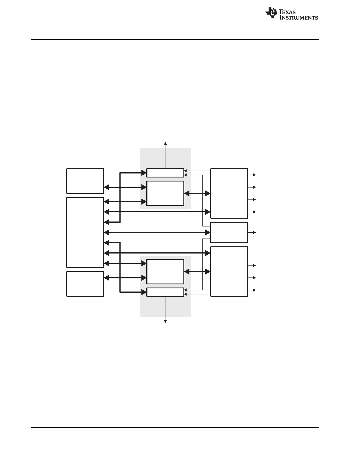
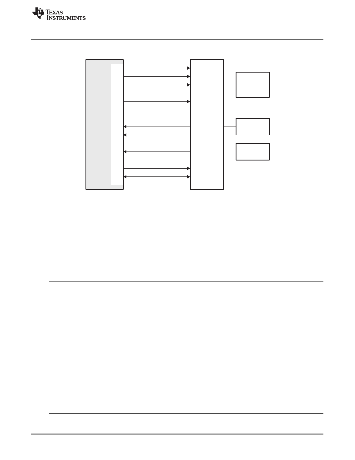
EMIC0
CPPIbuffer
manager+
CPPIRAM0
EMAC0
DMA
memory
transfercontrol
Peripheral
bus
MDIO
EMAC1
CPPIbuffer
manager+
CPPIRAM1
EMIC1
ToGEMs
ToGEMs
MII0/GMII0
RGMII0
RMII0
S3MII0
ToPHYs
RGMII1
RMII1
S3MII1
DMA
memory
transfercontrol
EMAC
Control0
Module
EMAC
Control1
Module
Introduction
• Single MDIO, shared by both EMAC modules.
1.3 Functional Block Diagram
Figure 1 shows the functional block diagram of the EMAC peripherals used in the TCI6486/C6472 device.
It consists mainly of:
• EMAC0
• EMAC1
• CPPI buffer manager per EMAC
• EMIC per EMAC
• MDIO
Figure 1. EMAC and MDIO Block Diagram
www.ti.com
12
C6472/TCI6486 EMAC/MDIO SPRUEF8F–March 2006–Revised November 2010
Copyright © 2006–2010, Texas Instruments Incorporated
Submit Documentation Feedback
Page 13

www.ti.com
The EMAC module provides an efficient interface between the TCI6486/C6472 core processor and the
networked community. The EMAC supports 10Base-T (10 Mbits/sec) and 100Base-TX (100 Mbits/sec) in
either half- or full-duplex mode, and 1000Base-T (1000 Mbits/sec) in full-duplex mode, with hardware flow
control and quality-of-service (QOS) support.
Each EMAC module has a communications port programming interface (CPPI) buffer manager to manage
8K of CPPI RAM. The EMAC uses four 32-bit words as buffer descriptors that point to different buffers in
the DSP memory. The CPUs create and maintain these buffer descriptors. The EMAC reads from and
writes to these buffer descriptors as it transfers data to or from the buffers.
The EMIC module associated with each EMAC takes a single set of interrupts from respective EMAC and
common MDIO and creates six different sets of TX, RX, and common interrupts to six cores of the
TCI6486/C6472 device. In addition, this module implements the interrupt pacing operation.
The control registers of the EMAC and MDIO modules are memory mapped into device memory space via
the device configuration bus.
The MDIO module implements the 802.3 serial management interface to interrogate and control up to 32
Ethernet PHYs connected to the device, using a shared two-wire bus. Application software uses the MDIO
module to configure the auto-negotiation parameters of each PHY attached to the EMAC, retrieve the
negotiation results, and configure required parameters in the EMAC module for correct operation. The
module is designed to allow almost transparent operation of the MDIO interface, with very little
maintenance from the core processor. A single MDIO is shared by both EMACs.
MACSEL0[2:0] and MACSEL1[1:0] are device configuration pins used to select the MII interface for
EMAC0 and EMAC1, respectively.
The MDIO communicates to PHY through two signals: MDCLK (output clock) and MDIO (bi-directional
data). For details of MDIO operation and signals, see Section 2.8. The device has two serial management
interfaces, although only one is used based on the interface selection of EMAC0. Table 1 shows the two
sets of pins associated with serial management interface. One serial management interface is for RGMII
(needed at 1.8-V HSTL buffer) and the other serial management interface is for non-RGMII interfaces
(needed at 3.3-V LVCMOS buffers).
Introduction
Table 1. Serial Management Interface Pins
Signal Description
GMDCLK MII/GMII/RMII/S3MII management clock. Available on 3.3-V LVCMOS buffers.
GMDIO MII/GMII/RMII/S3MII management data. Available on 3.3-V LVCMOS buffers.
RGMDCLK RGMII management clock. Available on 1.8-V HSTL buffers.
RGMDIO RGMII management data. Available on 1.8-V HSTL buffers.
As mentioned above, the management interface selection is based on the interface selection for EMAC0.
If MACSEL0 is programmed to select RGMII0, the 1.8-V serial management interface is selected
(RGMDIO, RGMDCLK), otherwise, the 3.3-V (GMDIO, GMDCLK) management interface is selected. Due
to this programmed selection, in some cases level shifters may have to be used for the management
interface. As an example, if the RGMII0 interface is selected for EMAC0 and the S3MII1 interface is
selected for EMAC1, the 1.8-V serial management interface (RGMDCLK and RGMDIO) is used. Since
S3MII PHY needs the 3.3-V management interface, level shifters have to be used to level translate these
HSTL pins.
Also note that EMAC1 can be enabled or disabled using the EMAC1_EN internal pulldown pin that
controls the I/O signals of EMAC1. The EMAC1_EN is also latched into the bit 12 of the DEVCTL register.
Table 2 describes the EMAC1_EN pin.
Table 2. EMAC1_EN Pin Description
Value Description
0 EMAC1 is disabled or not used.
Pulls on EMAC1 I/O are enabled (except RGMII pins) and the corresponding I/O
buffers are powered down.
SPRUEF8F–March 2006–Revised November 2010 C6472/TCI6486 EMAC/MDIO
Submit Documentation Feedback
Copyright © 2006–2010, Texas Instruments Incorporated
13
Page 14

Introduction
Table 2. EMAC1_EN Pin Description (continued)
Value Description
1 EMAC1 is enabled and used.
Pulls on EMAC1 I/O are disabled (except RGMII pins) and the corresponding I/O
buffers are powered up except RGMII output-only pins.
NOTE: RGMII buffers are HSTL buffers with no internal pulls. RGMII output only pins will always
be powered down even when the module is enabled.
EMAC1_EN is also software programmable through the DEVCTL register. A write to the DEVCTL register
is key-protected by the DEVCTL_KEY register. For details of MACSEL0, MACSEL1, and EMAC1_EN
decoding, see Section 2.3.
1.4 Industry Standard(s) Compliance Statement
The EMAC peripheral conforms to the IEEE 802.3 standard, describing the Carrier Sense Multiple Access
with Collision Detection (CSMA/CD) Access Method and Physical Layer specifications. ISO/IEC has also
adopted the IEEE 802.3 standard and re-designated it as ISO/IEC 8802-3:2000(E).
In difference from this standard, the EMAC peripheral integrated with the TCI6486/C6472 device does not
use the transmit coding error signal MTXER. Instead of driving the error pin when an underflow condition
occurs on a transmitted frame, the EMAC intentionally generates an incorrect check sum by inverting the
frame CRC so that the network detects the transmitted frame as an error.
www.ti.com
14
C6472/TCI6486 EMAC/MDIO SPRUEF8F–March 2006–Revised November 2010
Submit Documentation Feedback
Copyright © 2006–2010, Texas Instruments Incorporated
Page 15

www.ti.com
2 EMAC Functional Architecture
This section discusses the architecture and basic function of the EMAC peripheral.
2.1 Clock Control
The frequencies for the transmit and receive clocks are fixed by the IEEE 802.3 specification, as shown
below:
• 2.5 MHz at 10 Mbps
• 25 MHz at 100 Mbps
• 125 MHz at 1000 Mbps
All clock sources, with the exception of the EMAC peripheral bus clock, are sourced from the PLL2
controller. The PLL2 controller has 3 clocks for EMAC0: SYSCLK13, SYSCLK14, and SYSCLK15. For
EMAC0 operation, the SYSCLK14 divider is programmable and other clocks are fixed. The PLL multiplier
value of the PLL2 controller is also fixed. The PLL2 controller has 3 clocks for EMAC1: SYSCLK16,
SYSCLK17, and SYSCLK18. These clocks should remain fixed.
Table 3. EMAC Clock Specifications
Clock Divider Frequency Purpose
SYSCLK13 /2 250 MHz Used for RGMII0 only
SYSCLK14
SYSCLK15 /100 5 MHz Used for RGMII0 only
SYSCLK16 /2 250 MHz Used for RGMII1 only
SYSCLK17 /10 50 MHz Used for RGMII1 (default)
SYSCLK18 /100 5 MHz Used for RGMII1 only
/10 or 50 or 50 MHz used for RGMII (default
/4 125 MHz 125 MHz used for GMII
EMAC Functional Architecture
2.1.1 MII Clocking
The MII interface is supported by EMAC0 only. When MACSEL0 is set to zero (000b), the transmit and
receive clock sources are provided from an external PHY via the MTCLK and MRCLK pins. These clocks
are inputs to the EMAC module and operate at 2.5 MHz in 10-Mbps mode and at 25 MHz in 100-MHz
mode. The MII clocking interface is not used in 1000-Mbps mode. For timing purposes, data is transmitted
and received with reference to MTCLK and MRCLK, respectively.
2.1.2 RMII Clocking
The RMII interface is selected when MACSEL0 is set to 1 (001b) or MACSEL1 is set to 3 (11b). RMII
requires two clock sources, the peripheral bus clock and the reference clock (REF_CLK), input to the RMII
gasket. A 50-MHz clock from device input pin REFCLKx is supplied to the REF_CLK input of the RMII
gasket. The EMAC clocks the transmit and receive operations from the reference clock. The MTCLK and
MRCLK device pins are not used for this interface. The RMII protocol turns one data phase of an MII
transfer into two data phases at double the clock frequency. This is the driving factor for the 50-MHz
reference clock. Data at the I/O pins are running at 5 MHz in 10-Mbps mode and at 50 MHz in 100-Mbps
mode.
SPRUEF8F–March 2006–Revised November 2010 C6472/TCI6486 EMAC/MDIO
Submit Documentation Feedback
Copyright © 2006–2010, Texas Instruments Incorporated
15
Page 16

EMAC Functional Architecture
2.1.3 GMII Clocking
The GMII interface is available only on EMAC0 and requires two clock sources generated internally, the
peripheral bus clock and the RFTCLK inputs to the EMAC module. SYSCLK14 is programmed to /4 for
this interface to provide a 125-MHz clock to the RFTCLK input of EMAC. The GMII interface is selected by
programming MACSEL0 to 2 (010b). Transmit and receive clock sources for 10/100-Mbps modes are
provided from an external PHY via the MTCLK and MRCLK pins. For 1000-Mbps mode, the receive clock
is provided by an external PHY via the MRCLK pin. For transmit in 1000-Mbps mode, the clock is sourced
synchronous with the data, and is provided by the EMAC to be output on the GMTCLK pin.
For timing purposes, data in 10/100-Mbps mode is transmitted and received with reference to MTCLK and
MRCLK, respectively. For 1000-Mbps mode, receive timing is the same, but transmit is relative to
GMTCLK.
2.1.4 RGMII Clocking
The RGMII interface is selected by programming MACSEL0 to 3 (011b) and MACSEL1 to 2 (10b). RGMII
requires 4 internally generated clocks; peripheral bus clock and three reference clocks. The EMAC drives
the transmit clock, while an external PHY generates the receive clock. The reference clock drives the
device pin that gives the 125-MHz clock to the PHY; this enables the PHY to generate the receive clock
that is sent to EMAC.
The RGMII protocol takes a GMII data stream and turns it into an interface with half of the data bus width
and sends the same amount of data with a reduced pinout. The RGMII protocol also allows for dynamic
switching of the mode between 10/100/1000-Mbps modes. This negotiation data is embedded in the
incoming data stream from the external PHY. For timing purposes, data is transmitted and received with
respect to MTCLK and MRCLK, respectively.
The RGMII interface has separate I/O pins from the other EMAC pins because the interface voltage is
different from the other interfaces.
www.ti.com
2.1.5 S3MII Clocking
S3MII mode is selected by programming MACSEL0 to 5 (101b) and MACSEL1 to 1 (01b). The S3MII
gasket needs a 125-MHz continuous clock (125_CLK) supplied by an external source. It also needs a
peripheral bus clock as input. MTCLK and MRCLK are fixed at 125 MHz.
2.2 Memory Map
The EMAC includes an internal memory that holds information about the Ethernet packets that are
received or transmitted. This internal RAM is 2K x 32 bits in size. The data can be written to and read from
the EMAC internal memory via either the EMAC or the CPU. It stores buffer descriptors that are 4 words
(16 bytes) deep. This 8K local memory holds enough information to transfer up to 512 Ethernet packets
without CPU intervention.
The packet buffer descriptors can be put in internal processor memory (L2) on the TCI6486/C6472 device.
There are some trade-offs in terms of cache performance and throughput when the descriptors are put in
L2 versus when they are put in EMAC internal memory. The cache performance improves when the buffer
descriptors are put in the internal memory. However, the EMAC throughput is better when the descriptors
are put in the local EMAC RAM.
16
C6472/TCI6486 EMAC/MDIO SPRUEF8F–March 2006–Revised November 2010
Submit Documentation Feedback
Copyright © 2006–2010, Texas Instruments Incorporated
Page 17

www.ti.com
2.3 System-Level Connections
On the TCI6486/C6472 device, EMAC0 and EMAC1 support the following different types of interfaces to
physical layer devices (PHYs) or switches. Each EMAC can be configured to only one interface at any
given time. EMAC0 interface is selected by programming MACSEL0 [2:0] pins (see Table 4) and EMAC1
interface is selected by programming MACSEL1 [1:0] pins (see Table 5).
Table 4. EMAC0 Interface Selection Pins
MACSEL0 [2:0] Interface
Table 5. EMAC1 Interface Selection Pins
MACSEL1 [1:0] Interface
EMAC Functional Architecture
000 MII
001 RMII
010 GMII
011 RGMII
100 Not used
101 S3MII
110 Not used
111 Not used
00 Not used
01 S3MII
10 RGMII
11 RMII
Table 6 explains the decoding of MACSEL0 [2:0], MACSEL1[1:0], and EMAC1_EN of the DEVCTL
register.
Table 6. MACSEL0[2:0], MACSEL1[1:0], and EMAC1_EN Decoding
MACSEL02 MACSEL01 MACSEL00 MACSEL11 MACSEL10 EMAC_EN EMAC0 EMAC1
0 0 0 X X 0 MII None
0 0 0 0 X 1 MII None
0 0 0 1 0 1 MII RGMII
0 1 0 X X 0 GMII None
0 1 0 0 X 1 GMII None
0 1 0 1 0 1 GMII RGMII
0 0 1 X X 0 RMII None
0 1 1 X X 0 RGMII None
1 0 0 X X 0 None None
1 0 1 X X 0 S3MII None
0 0 1 0 0 1 RMII None
0 0 1 0 1 1 RMII S3MII
0 0 1 1 0 1 RMII RGMII
0 0 1 1 1 1 RMII RMII
0 1 1 0 0 1 RGMII None
0 1 1 0 1 1 RGMII S3MII
0 1 1 1 0 1 RGMII RGMII
0 1 1 1 1 1 RGMII RMII
1 0 0 0 0 1 None None
1 0 0 0 1 1 None S3MII
1 0 0 1 0 1 None RGMII
SPRUEF8F–March 2006–Revised November 2010 C6472/TCI6486 EMAC/MDIO
Submit Documentation Feedback
Copyright © 2006–2010, Texas Instruments Incorporated
17
Page 18
MTCLK
MTXD[3−0]
MTXEN
MCOL
MCRS
MRCLK
MRXD[3−0]
MRXDV
MRXER
MDCLK
MDIO
2.5 MHZ
or
25 MHz
Physical
layer
device
(PHY)
System
core
EMAC
MDIO
Transformer
RJ-45
EMAC Functional Architecture
Table 6. MACSEL0[2:0], MACSEL1[1:0], and EMAC1_EN Decoding (continued)
MACSEL02 MACSEL01 MACSEL00 MACSEL11 MACSEL10 EMAC_EN EMAC0 EMAC1
1 0 0 1 1 1 None RMII
1 0 1 0 0 1 S3MII None
1 0 1 0 1 1 S3MII S3MII
1 0 1 1 0 1 S3MII RGMII
1 0 1 1 1 1 S3MII RMII
1 1 1 X X 0 None None
1 1 1 0 0 1 None None
1 1 1 0 1 1 None S3MII
1 1 1 1 0 1 None RGMII
1 1 1 1 1 1 None RMII
2.3.1 Media Independent Interface (MII) Connections
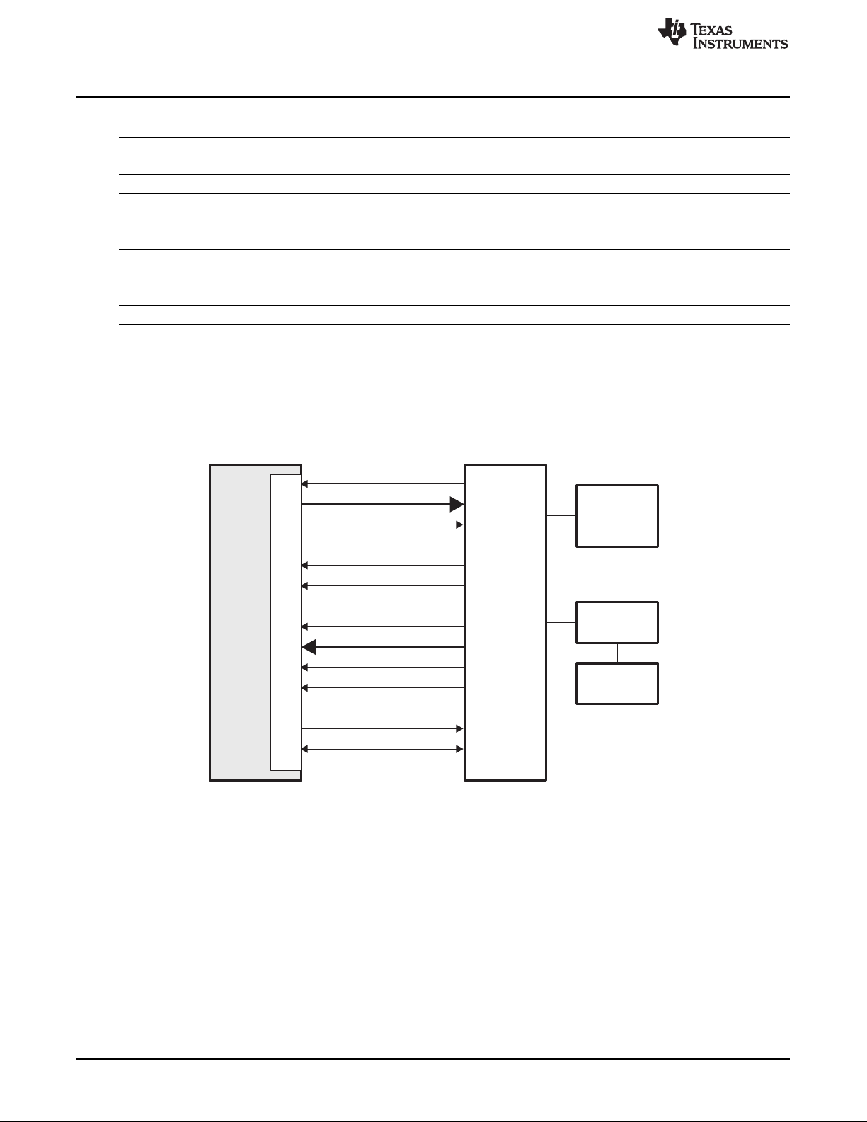
Figure 2 shows a TCI6486/C6472 device with integrated EMAC and MDIO interfaced to the PHY via an
MII connection. This interface is only available in 10 Mbps and 100 Mbps modes.
Figure 2. Ethernet Configuration with MII Interface
www.ti.com
Table 7 summarizes the individual EMAC and MDIO signals for the MII interface. For more information,
refer to either the IEEE 802.3 standard or ISO/IEC 8802-3:2000(E).
The EMAC module does not include a transmit error (MTXER) pin. If a transmit error occurs, CRC
inversion is used to negate the validity of the transmitted frame.
18
C6472/TCI6486 EMAC/MDIO SPRUEF8F–March 2006–Revised November 2010
Copyright © 2006–2010, Texas Instruments Incorporated
Submit Documentation Feedback
Page 19

www.ti.com
EMAC Functional Architecture
Table 7. EMAC and MDIO Signals for MII Interface
Signal Name I/O Description
MTCLK I Transmit clock (MTCLK). The transmit clock is a continuous clock that provides the timing reference
for transmit operations. The MTXD and MTXEN signals are tied to this clock. The clock is generated
by the PHY and is 2.5 MHz at 10-Mbps operation and 25 MHz at 100-Mbps operation.
MTXD[3:0] O Transmit data (MTXD). The transmit data pins are a collection of 4 data signals comprising 4 bits of
data. MTDX0 is the least-significant bit (LSB). The signals are synchronized by MTCLK and valid
only when MTXEN is asserted.
MTXEN O Transmit enable (MTXEN). The transmit enable signal indicates that the MTXD pins are generating
nibble data for use by the PHY. It is driven synchronously to MTCLK.
MCOL I Collision detected (MCOL). The MCOL pin is asserted by the PHY when it detects a collision on the
network. It remains asserted while the collision condition persists. This signal is not necessarily
synchronous to MTCLK nor MRCLK. This pin is used in half-duplex operation only.
MCRS I Carrier sense (MCRS). The MCRS pin is asserted by the PHY when the network is not idle in either
transmit or receive. The pin is de-asserted when both transmit and receive are idle. This signal is not
necessarily synchronous to MTCLK or MRCLK. This pin is used in half-duplex operation only.
MRCLK I Receive clock (MRCLK). The receive clock is a continuous clock that provides the timing reference
for receive operations. The MRXD, MRXDV, and MRXER signals are tied to this clock. The clock is
generated by the PHY and is 2.5 MHz at 10-Mbps operation and 25 MHz at 100-Mbps operation.
MRXD[3:0] I Receive data (MRXD). The receive data pins are a collection of 4 data signals comprising 4 bits of
data. MRDX0 is the least-significant bit (LSB). The signals are synchronized by MRCLK and valid
only when MRXDV is asserted.
MRXDV I Receive data valid (MRXDV). The receive data valid signal indicates that the MRXD pins are
generating nibble data for use by the EMAC. It is driven synchronously to MRCLK.
MRXER I Receive error (MRXER). The receive error signal is asserted for one or more MRCLK periods to
indicate that an error was detected in the received frame. This is meaningful only during data
reception when MRXDV is active.
MDCLK O Management data clock (MDCLK). The MDIO data clock is sourced by the MDIO module on the
system. It is used to synchronize MDIO data access operations done on the MDIO pin. The
frequency of this clock is controlled by the CLKDIV bits in the MDIO control register (CONTROL).
MDIO I/O Management data input output (MDIO). The MDIO pin drives PHY management data into and out of
the PHY by way of an access frame consisting of start of frame, read/write indication, PHY address,
register address, and data bit cycles. The MDIO pin acts as an output for everything except the data
bit cycles, when the pin acts as an input for read operations.
When the device is interfaced to an Ethernet switch via an MII interface, the carrier sense (MCRS) and
collision (MCOL) signals are not necessary since full-duplex operation is forced.
On the TCI6486/C6472 device, the MII Ethernet interface is available only on EMAC0. MII0 pins are
multiplexed with other non-RGMII pins (RMII1, S3MII1). due to this multiplexing, when the MII0 interface is
selected on EMAC0, except for RGMII1, no Ethernet interface is available on EMAC1.
SPRUEF8F–March 2006–Revised November 2010 C6472/TCI6486 EMAC/MDIO
Submit Documentation Feedback
Copyright © 2006–2010, Texas Instruments Incorporated
19
Page 20
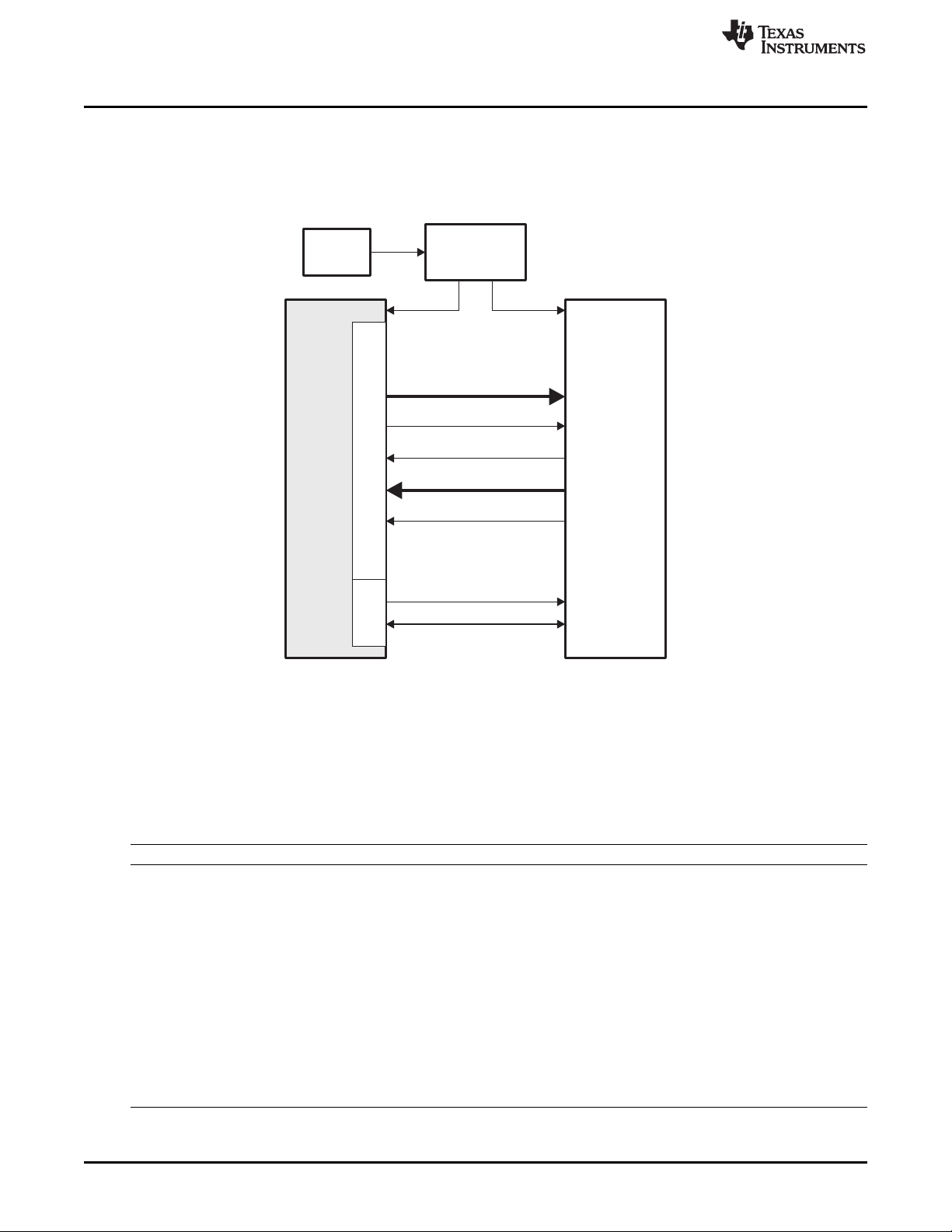
MDCLK
MDIO
RMTXD[1−0]
RMTXEN
RMCRSDV
RMRXD[1−0]
RMRXER
Physical
layer
device
(PHY)
EMAC
MDIO
System
core
RMREFCLK RMREFCLK
50-MHz
zero-delay
clock buffer
50-MHz
XO
EMAC Functional Architecture
2.3.2 Reduced Media Independent Interface (RMII) Connections
Figure 3 shows a TCI6486/C6472 device with integrated EMAC and MDIO interfaced to the PHY via an
RMII connection. This interface is available only in 10-Mbps and 100-Mbps modes.
Figure 3. Ethernet Configuration with RMII Interface
www.ti.com
The RMII interface has the same functionality as the MII, but it does so with a reduced number of pins,
thus lowering the total cost for an application. In devices incorporating many PHY interfaces such as
switches, the number of pins can add significant cost as the port counts increase. Table 8 summarizes the
individual EMAC and MDIO signals for the RMII interface.
The RMII interface does not include an MCOL signal. A collision is detected from the receive and transmit
data delimiters. The data signals are 2 bits wide, and a single reference clock must be provided to the
MAC, operating at 50 MHz to sustain the same data rate as MII.
Signal Name I/O Description
RMTXD[1-0] O Transmit data (RMTXD). The transmit data pins are a collection of 2 data signals comprising 2 bits
RMTXEN O Transmit enable (RMTXEN). The transmit enable signal indicates that the RMTXD pins are
RMCRSDV I Carrier sense/receive data valid (RMCRSDV). The RMCRSDV pin is asserted by the PHY when the
RMREFCLK I Reference clock (RMREFCLK). A 50-MHz clock must be provided through this pin for RMII
RMRXD[1-0] I Receive data (RMRXD). The receive data pins are a collection of 2 data signals comprising 2 bits of
Table 8. EMAC and MDIO Signals for RMII Interface
of data. RMTDX0 is the least-significant bit (LSB). The signals are synchronized to the RMII
reference clock and valid only when RMTXEN is asserted.
generating nibble data for use by the PHY. It is driven synchronously to the RMII reference clock.
network is not idle in either transmit or receive. The data on RMRXD is considered valid once the
RMCRSDV signal is asserted. The pin is de-asserted when both transmit and receive are idle. The
assertion of this signal is asynchronous to the RMII reference clock.
operation.
data. RMRDX0 is the least-significant bit (LSB). The signals are synchronized to the RMII reference
clock and valid only when RMCRSDV is asserted. In 10-Mbps operation, RMRXD is sampled every
tenth cycle of the RMII reference clock.
20
C6472/TCI6486 EMAC/MDIO SPRUEF8F–March 2006–Revised November 2010
Copyright © 2006–2010, Texas Instruments Incorporated
Submit Documentation Feedback
Page 21
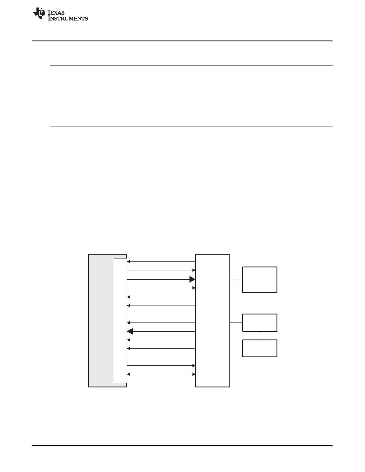
MTCLK
MTXD[7−0]
MTXEN
MCOL
MCRS
MRCLK
MRXD[7−0]
MRXDV
MRXER
MDCLK
MDIO
Physical
layer
device
(PHY)
System
core
Transformer
2.5 MHz,
25 MHz,
or 125 MHz
RJ−45
EMAC
MDIO
GMTCLK
www.ti.com
The 50-MHz reference clock (RMREFCLK) for the RMII gasket is sourced externally through a zero-delay
clock buffer. If multiple RMII PHY ports are used, all device RMII reference clocks must come from same
zero-delay clock buffer.
On the TCI6486/C6472 device, RMII pins are multiplexed with other non-RGMII pins. When using the
RMII0 port on EMAC0, there are no restrictions on the available EMAC1 Ethernet interfaces (RMII1,
S3MII1, and RGMII1 are useable). When using the RMII1 port on EMAC1, the EMAC0 Ethernet interfaces
not available due to pin multiplexing are GMII0/MII0. The RMII0, S3MII0, and RGMII0 ports are available
on EMAC0 Ethernet interfaces when using the RMII1 port on EMAC1.
If the device is interfaced to an Ethernet switch through the RMII interface, all device RMII reference
clocks should be externally sourced from the same zero-delay clock buffer.
EMAC Functional Architecture
Table 8. EMAC and MDIO Signals for RMII Interface (continued)
Signal Name I/O Description
RMRXER I Receive error (RMRXER). The receive error signal is asserted for one or more reference clock
periods to indicate that an error was detected in the received frame. This is meaningful only during
data reception when RMCRSDV is active. It is driven synchronously to the RMII reference clock.
MDCLK O Management data clock (MDCLK). The MDIO data clock is sourced by the MDIO module on the
system. It is used to synchronize MDIO data access operations done on the MDIO pin. The
frequency of this clock is controlled by the CLKDIV bits in the MDIO control register (CONTROL).
MDIO I/O Management data input output (MDIO). The MDIO pin drives PHY management data into and out of
the PHY by way of an access frame consisting of start of frame, read/write indication, PHY address,
register address, and data bit cycles. The MDIO pin acts as an output for everything except the data
bit cycles, when the pin acts as an input for read operations.
2.3.3 Gigabit Media Independent Interface (GMII) Connections
Figure 4 shows a device with integrated EMAC and MDIO interfaced to the PHY via a GMII connection.
This interface is available in 10 Mbps, 100 Mbps, and 1000 Mbps modes.
Figure 4. Ethernet Configuration with GMII Interface
The GMII interface supports 10/100/1000 Mbps modes. Only full-duplex mode is available in 1000 Mbps
mode. In 10/100 Mbps modes, the GMII interface acts like an MII interface, and only the lower 4 bits of
data are transferred for each of the data buses.
Table 9 summarizes the individual EMAC and MDIO signals for the GMII interface.
SPRUEF8F–March 2006–Revised November 2010 C6472/TCI6486 EMAC/MDIO
Submit Documentation Feedback
Copyright © 2006–2010, Texas Instruments Incorporated
21
Page 22

EMAC Functional Architecture
Signal Name I/O Description
MTCLK I Transmit clock (MTCLK). The transmit clock is a continuous clock that provides the timing reference
GMTCLK O GMII source synchronous transmit clock (GMTCLK). This clock is used in 1000 Mbps mode only,
MTXD[7-0] O Transmit data (MTXD). The transmit data pins are a collection of 8 data signals comprising 8 bits of
MTXEN O Transmit enable (MTXEN). The transmit enable signal indicates that the MTXD pins are generating
MCOL I Collision detected (MCOL). The MCOL pin is asserted by the PHY when it detects a collision on the
MCRS I Carrier sense (MCRS). The MCRS pin is asserted by the PHY when the network is not idle in either
MRCLK I Receive clock (MRCLK). The receive clock is a continuous clock that provides the timing reference
MRXD[7-0] I Receive data (MRXD). The receive data pins are a collection of 8 data signals comprising 8 bits of
MRXDV I Receive data valid (MRXDV). The receive data valid signal indicates that the MRXD pins are
MRXER I Receive error (MRXER). The receive error signal is asserted for one or more MRCLK periods to
MDCLK O Management data clock (MDCLK). The MDIO data clock is sourced by the MDIO module on the
MDIO I/O Management data input output (MDIO). The MDIO pin drives PHY management data into and out of
www.ti.com
Table 9. EMAC and MDIO Signals for GMII Interface
for transmit operations in 10/100 Mbps mode. The MTXD and MTXEN signals are tied to this clock
when in 10/100 Mbps mode. The clock is generated by the PHY and is 2.5 MHz at 10-Mbps
operation, and 25 MHz at 100-Mbps operation.
providing a continuous 125 MHz frequency for transmit operations. The MTXD and MTXEN signals
are tied to this clock when in Gigabit mode. The clock is generated by the EMAC and is 125 MHz.
data. MTDX0 is the least-significant bit (LSB). The signals are synchronized by MTCLK in 10/100
Mbps mode, and by GMTCLK in Gigabit mode, and valid only when MTXEN is asserted.
nibble data for use by the PHY. It is driven synchronously to MTCLK in 10/100 Mbps mode, and to
GMTCLK in Gigabit mode.
network. It remains asserted while the collision condition persists. This signal is not necessarily
synchronous to MTCLK nor MRCLK. This pin is used in half-duplex operation only.
transmit or receive. The pin is de-asserted when both transmit and receive are idle. This signal is not
necessarily synchronous to MTCLK nor MRCLK. This pin is used in half-duplex operation only.
for receive operations. The MRXD, MRXDV, and MRXER signals are tied to this clock. The clock is
generated by the PHY and is 2.5 MHz at 10-Mbps operation, 25 MHz at 100-Mbps operation and
125 MHz at 1000-Mbps operation.
data. MRDX0 is the least-significant bit (LSB). The signals are synchronized by MRCLK and valid
only when MRXDV is asserted.
generating nibble data for use by the EMAC. It is driven synchronously to M RCLK.
indicate that an error was detected in the received frame. This is meaningful only during data
reception when MRXDV is active.
system. It is used to synchronize MDIO data access operations done on the MDIO pin. The
frequency of this clock is controlled by the CLKDIV bits in the MDIO control register (CONTROL).
the PHY by way of an access frame consisting of start of frame, read/write indication, PHY address,
register address, and data bit cycles. The MDIO pin acts as an output for everything except the data
bit cycles, when the pin acts as an input for read operations.
When the TCI6486/C6472 device is interfaced to an Ethernet switch via the GMII interface, the carrier
sense (MCRS) and collision (MCOL) signals are not necessary since full-duplex operation is forced.
On the device, the GMII Ethernet interface is available only on EMAC0 of the device. GMII0 pins are
multiplexed with other non-RGMII pins (RMII1, S3MII1). Due to this multiplexing, when the MII0 interface
is selected on EMAC0, except for RGMII1, no Ethernet interface is available on EMAC1.
2.3.4 Reduced Gigabit Media Independent Interface (RGMII) Connections
Figure 5 shows a TCI6486/C6472 device with integrated EMAC and MDIO interfaced to the PHY via an
RGMII connection. This interface is available in 10 Mbps, 100 Mbps, and 1000 Mbps modes.
22
C6472/TCI6486 EMAC/MDIO SPRUEF8F–March 2006–Revised November 2010
Copyright © 2006–2010, Texas Instruments Incorporated
Submit Documentation Feedback
Page 23
RGTXC
RGTXD[3−0]
RGTXCTL
RGREFCLK
RGRXC
RGRXD[3−0]
RGRXCTL
RGMDCLK
RGMDIO
Physical
layer
device
(PHY)
System
core
Transformer
2.5 MHz
25 MHz,
or 125 MHz
RJ−45
EMAC
MDIO
www.ti.com
The RGMII interface is a reduced pin alternative to the GMII interface. The data paths are reduced, control
signals are multiplexed together, and both edges of the clock are used.
The RGMII interface does not include a MCOL and a MCRS signal for half-duplex mode (only available in
10/100 Mbps mode).
Carrier sense (MCRS) is indicated by one of the following cases instead:
• MRXDV signal (multiplexed in the RGRXCTL signal) is true
• MRXDV is false, MRXERR (multiplexed in the RGRXCTL signal) is true, and a value of FFh exists on
Table 10 summarizes the individual EMAC and MDIO signals for the RGMII interface.
EMAC Functional Architecture
Figure 5. Ethernet Configuration with RGMII Interface
the RGRXD[3:0] simultaneously
Table 10. EMAC and MDIO Signals for RGMII Interface
Signal Name I/O Description
RGTXC O Transmit clock (RGTXC). The transmit clock is a continuous clock that provides the timing reference
RGTXD[3-0] O Transmit data (RGTXD). The transmit data pins are a collection of 4 data signals comprising 4 bits of
RGTXCTL O Transmit enable (RGTXCTL). The transmit enable signal indicates that the RGTXD pins are
RGREFCLK O Reference clock (RGREFCLK). This 125-MHz reference clock is provided as a convenience. It can
RGRXC I Receive clock (RGRXC). The receive clock is a continuous clock that provides the timing reference
RGRXD[3-0] I Receive data (RGRXD). The receive data pins are a collection of 4 data signals comprising 4 bits of
SPRUEF8F–March 2006–Revised November 2010 C6472/TCI6486 EMAC/MDIO
Submit Documentation Feedback
for transmit operations. The RGTXD and RGTXCTL signals are tied to this clock. The clock is driven
by the EMAC and is 2.5 MHz at 10-Mbps operation, 25 MHz at 100-Mbps operation, and 125 MHz at
1000-Mbps operation.
data. RGTDX0 is the least-significant bit (LSB). The signals are synchronized by RGTXC and valid
only when RGTXCTL is asserted. The lower 4 bits of data are transmitted on the rising edge of the
clock, and the higher 4 bits of data are transmitted on the falling edge of the RGTXC.
generating nibble data for use by the PHY. It is driven synchronously to RGTXC.
be used as a clock source to the PHY, so that the PHY may generate the RGRXC clock to be sent
to EMAC. This clock is stopped while the device is in reset.
for receive operations. The RGRXD, and RGRXCTL signals are tied to this clock. The clock is
generated by the PHY and is 2.5 MHz at 10-Mbps operation, 25 MHz at 100-Mbps operation, and
125 MHz at 1000-Mbps operation.
data. RGRDX0 is the least-significant bit (LSB). The signals are synchronized by RGRXC and valid
only when RGRXCTL is asserted. The lower 4 bits of data are received on the rising edge of the
clock, and the higher 4 bits of data are received on the falling edge of the RGRXC.
Copyright © 2006–2010, Texas Instruments Incorporated
23
Page 24

EMAC Functional Architecture
Table 10. EMAC and MDIO Signals for RGMII Interface (continued)
Signal Name I/O Description
RGRXCTL I Receive control (RGRXCTL). The receive control data has the receive data valid (MRXDV) signal on
RGMDCLK O Management data clock (RGMDCLK). The RGMDIO data clock is sourced by the MDIO module. It
RGMDIO I/O Management data input output (RGMDIO). The RGMDIO pin drives PHY management data into and
RGMII pins are not multiplexed with other interfaces and are HSTL I/O having voltages different than other
interfaces. (RGMII pins are 1.5-V/1.8-V HSTL I/O, whereas other interfaces are 3.3-V LVCMOS I/O). The
unused pins of the RGMII PHY should be pulled down to avoid floating inputs.
www.ti.com
the rising edge of the receive clock, and a derivative of receive data valid and receive error
(MRXER) on the falling edge of RGRXC.
When receiving a valid frame with no errors, MRXDV = TRUE is generated as a logic high on the
rising edge on RGRXC and MRXER = FALSE is generated as a logic high on the falling edge of
RGRXC.
When no frame is being received, MRXDV = FALSE is generated as a logic low on the rising edge
of RGRXC and MRXER = FALSE is generated as a logic low on the falling edge of RGRXC.
When receiving a valid frame with errors, MRXDV = TRUE is generated as a logic high on the rising
edge of RGRXC and MRXER = TRUE is generated as a logic low on the falling edge of RGRXC.
synchronizes MDIO data access operations done on the RGMDIO pin. The frequency of this clock is
controlled by the CLKDIV bits in the MDIO control register (CONTROL).
out of the PHY by way of an access frame consisting of start of frame, read/write indication, PHY
address, register address, and data bit cycles. The RGMDIO pin acts as an output for everything
except the data bit cycles, when the pin acts as an input for read operations.
24
C6472/TCI6486 EMAC/MDIO SPRUEF8F–March 2006–Revised November 2010
Submit Documentation Feedback
Copyright © 2006–2010, Texas Instruments Incorporated
Page 25
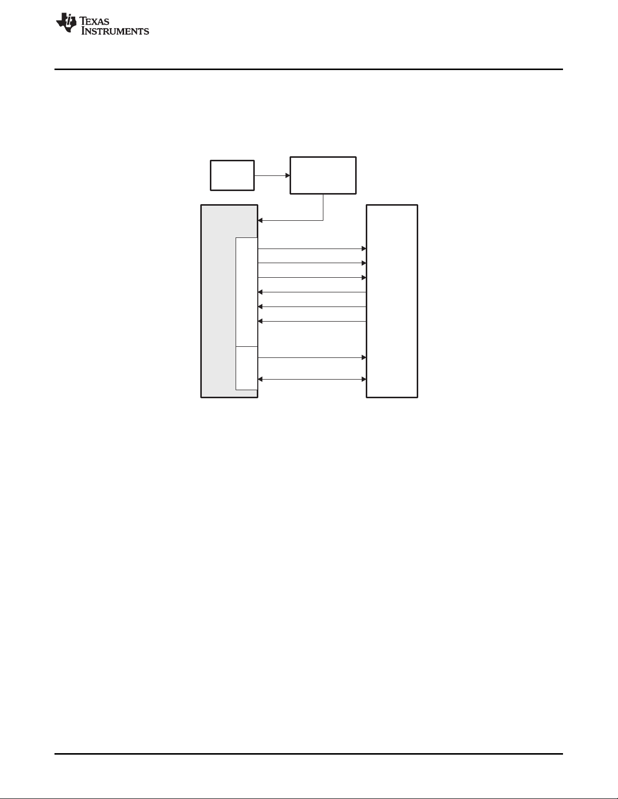
TX_CLK
TXD
TX_SYNC
RX_CLK
RXD
RX_SYNC
MDCLK
MDIO
EMAC
MDIO
System
core
Physical
layer
device
(PHY)
MHZ_125_CLK
125-MHz
zero-delay
clockbuffer
125-MHz
XO
www.ti.com
EMAC Functional Architecture
2.3.5 Source Synchronous Serial Media Independent Interface (S3MII) Connections
Figure 6 shows a TCI6486/C6472 device with an integrated EMAC and MDIO interface via S3MII
connections connected to a PHY. The S3MII interface supports source synchronous 10-Mbps and
100-Mbps operations with full- and half-duplex support.
Figure 6. Ethernet Configuration with S3MII Interface
SPRUEF8F–March 2006–Revised November 2010 C6472/TCI6486 EMAC/MDIO
Submit Documentation Feedback
Copyright © 2006–2010, Texas Instruments Incorporated
25
Page 26

EMAC Functional Architecture
Table 11 summarizes the individual EMAC and MDIO signals for the S3MII interface.
Signal Name I/O Description
TX_CLK O Transmit clock. The transmit clock is a continuous clock that provides the timing reference for
TX_SYNC O Transmit Synchronization. The TX_SYNC signal is used to synchronize the TXD data signal. This
TXD O Transmit Data. The transmit data is synchronized with a transmit clock and a transmit
RX_CLK I Transmit clock. The transmit clock is a continuous clock that provides the timing reference for
RX_SYNC I Receive Synchronization. The RX_SYNC signal is used to synchronize the RXD data signal. This
RXD I Receive Data. The receive data is synchronized with a receive clock and a receive synchronization
MDCLK O Management data clock (MDCLK). The MDIO data clock is sourced by the MDIO module. It
MDIO I/O Management data input output (MDIO). The MDIO pin drives PHY management data into and out of
www.ti.com
Table 11. EMAC and MDIO Signals for S3MII Interface
transmit operations. The TXD and TX_SYNC signals are tied to this clock. This clock is 125 MHz at
10- and 100-Mbps operations.
signal is synchronized with a 125-MHz clock.
synchronization signal.
transmit operations. The RXD and RX_SYNC signals are tied to this clock. This clock is 125 MHz at
10- and 100-Mbps operations.
signal is synchronized with a 125-MHz clock.
signal.
synchronizes MDIO data access operations done on the MDIO pin. The frequency of this clock is
controlled by the CLKDIV bits in the MDIO control register (CONTROL).
the PHY via an access frame consisting of start-of-frame, read/write indication, PHY address,
register address, and data-bit cycles. The MDIO pin acts as an output for everything except the
data-bit cycles, when the pin acts as an input for read operations.
The TCI6486/C6472 device S3MII pins are multiplexed with other non-RGMII pins. When using the
S3MII0 port on EMAC0, there are no restrictions on the available EMAC1 Ethernet interfaces (RMII1,
S3MII1, and RGMII1 are useable). When using the S3MII1 port on EMAC1, the EMAC0 Ethernet
interfaces not available due to pin multiplexing are GMII0/MII0. The RMII0, S3MII0, and RGMII0 ports are
available on EMAC0 Ethernet interfaces.
In a multi-PHY situation, where PHY has only one TX_SYNC for all ports, external logic is needed to
synchronize the TX_SYNC signals from multiple ports or TCI6486/C6472 devices. The TXD signal from
the multiple ports should also be synchronized using external logic since the clock-phase relation of
different TCI6486/C6472 devices can be different. Figure 7 demonstrates the example mutli-PHY
configuration for S3MII.
26
C6472/TCI6486 EMAC/MDIO SPRUEF8F–March 2006–Revised November 2010
Submit Documentation Feedback
Copyright © 2006–2010, Texas Instruments Incorporated
Page 27
TXD
TX_SYNC
TX_CLK
RXD
RX_SYNC
RX_CLK
MHZ_125_CLK
Device #1
TXD
TX_SYNC
TX_CLK
RXD
RX_SYNC
RX_CLK
MHZ_125_CLK
Device #2
TXD
TX_SYNC
TX_CLK
RXD
RX_SYNC
RX_CLK
MHZ_125_CLK
Device #n
125-MHz
zero-delay
clock buffer
125-MHz
XO
Low-skew
buffer
Zero-delay
clock buffer
External
logic
element
S3MII
multi-PHY
TX_CLK
TX_SYNC
P0_TXD
P0_RXD
P1_TXD
P1_RXD
Pn_TXD
Pn_RXD
RX_SYNC
RX_CLK
www.ti.com
EMAC Functional Architecture
Figure 7. S3MII Multi-PHY Configuration
SPRUEF8F–March 2006–Revised November 2010 C6472/TCI6486 EMAC/MDIO
Submit Documentation Feedback
Copyright © 2006–2010, Texas Instruments Incorporated
27
Page 28
TXD
TX_SYNC
TX_CLK
RXD
RX_SYNC
RX_CLK
MHZ_125_CLK
Device #1
TXD
TX_SYNC
TX_CLK
RXD
RX_SYNC
RX_CLK
MHZ_125_CLK
Device #2
TXD
TX_SYNC
TX_CLK
RXD
RX_SYNC
RX_CLK
MHZ_125_CLK
Device #n
125-MHz
zero-delay
clock buffer
125-MHz
XO
Low-skew
buffer
Zero-delay
clock buffer
External
logic
element
S3MII
switch
TX_CLK
TX_SYNC
P0_TXD
P0_RXD
P1_TXD
P1_RXD
Pn_TXD
Pn_RXD
RX_SYNC
RX_CLK
EMAC Functional Architecture
In the case of the S3MII switch, where the switch has only one TX_SYNC for all ports, external logic is
needed to synchronize the TX_SYNC signals from multiple ports or TCI6486/C6472 devices. The TXD
signal from the multiple ports should also be synchronized using external logic since the clock-phase
relation of different TCI6486/C6472 devices can be different. Figure 8 demonstrates the example
mutli-PHY configuration for S3MII.
www.ti.com
Figure 8. S3MII Switch Configuration
28
C6472/TCI6486 EMAC/MDIO SPRUEF8F–March 2006–Revised November 2010
Copyright © 2006–2010, Texas Instruments Incorporated
Submit Documentation Feedback
Page 29

Preamble
SFD
Destination
Source
Len Data
7 1 6 6 2 46 − (RXMAXLEN - 18) 4
FCS
Number of bytes
Legend: SFD = Start Frame Delimiter; FCS = Frame Check Sequence (CRC)
www.ti.com
2.4 Ethernet Protocol Overview
Ethernet provides a reliable, connectionless service to a networking application. A brief overview of the
ethernet protocol follows. For more information on the carrier sense multiple access with collision
detection (CSMA/CD) access method (ethernet's multiple access protocol), see the IEEE 802.3 standard
document.
2.4.1 Ethernet Frame Format
All the ethernet technologies use the same frame structure. The format of an ethernet frame is shown in
Figure 9 and described in Table 12. The ethernet packet is the collection of bytes representing the data
portion of a single ethernet frame on the wire (shown outlined in bold in Figure 9).
The ethernet frames are of variable lengths, with no frame smaller than 64 bytes or larger than
RXMAXLEN bytes (header, data, and CRC).
EMAC Functional Architecture
Figure 9. Ethernet Frame
Table 12. Ethernet Frame Description
Field Bytes Description
Preamble 7 These 7 bytes have a fixed value of 55h. They wake up the receiving EMAC ports and
Start-of-Frame 1 This field with a value of 5Dh immediately follows the preamble pattern and indicates
Delimiter the start of important data.
Destination 6 This field contains the Ethernet MAC address of the intended EMAC port for the frame.
address It may be an individual or multicast (including broadcast) address. If the destination
Source 6 This field contains the MAC address of the Ethernet port that transmits the frame to the
address Local Area Network.
Len 2 The length field indicates the number of EMAC client data bytes contained in the
Data 46 to (RXMAXLEN - 18) This field carries the datagram containing the upper layer protocol frame (the IP layer
Frame Check 4 A cyclic redundancy check (CRC) is used by the transmit and receive algorithms to
Sequence generate a CRC value for the FCS field. The frame check sequence covers the 60 to
synchronize their clocks to that of the sender's clock.
EMAC port receives an Ethernet frame with a destination address that does not match
any of its MAC physical addresses, and no promiscuous, multicast or broadcast
channel is enabled, it discards the frame.
subsequent data field of the frame. This field can also be used to identify the data type
carried by the frame.
datagram). The maximum transfer unit (MTU) of Ethernet is (RXMAXLEN - 18) bytes.
Therefore, if the upper layer protocol datagram exceeds (RXMAXLEN - 18) bytes, the
host must fragment the datagram and send it in multiple Ethernet packets. The
minimum size of the data field is 46 bytes. Thus, if the upper layer datagram is less
then 46 bytes, the data field must be extended to 46 bytes by appending extra bits after
the data field, but prior to calculating and appending the FCS.
(RXMAXLEN - 4) bytes of the packet data. Note that the 4-byte FCS field may not be
included as part of the packet data, depending on the EMAC configuration.
SPRUEF8F–March 2006–Revised November 2010 C6472/TCI6486 EMAC/MDIO
Submit Documentation Feedback
Copyright © 2006–2010, Texas Instruments Incorporated
29
Page 30

EMAC Functional Architecture
2.4.2 Multiple Access Protocol
Nodes in an ethernet local area network are interconnected by a broadcast channel. As a result, when an
EMAC port transmits a frame, all of the adapters on the local network receive the frame. Carrier sense
multiple access with collision detection (CSMA/CD) algorithms are used when the EMAC operates in
half-duplex mode. When operating in full-duplex mode, there is no contention for use of a shared medium,
because there are exactly two ports on the local network.
Each port runs the CSMA/CD protocol without explicit coordination with the other ports on the ethernet
network.
Within a specific port, the CSMA/CD protocol is as follows:
1. The port obtains data from upper layer protocols at its node, prepares an ethernet frame, and puts the
frame in a buffer.
2. If the port senses that the medium is idle, it starts to transmit the frame. If the port senses that the
transmission medium is busy, it waits until it senses no signal energy (plus an inter-packet gap time)
and then starts to transmit the frame.
3. While transmitting, the port monitors for the presence of signal energy coming from other ports. If the
port transmits the entire frame without detecting signal energy from other ethernet devices, the port is
finished with the frame.
4. If the port detects signal energy from other ports while transmitting, it stops transmitting its frame and
instead transmits a 48-bit jam signal.
5. After transmitting the jam signal, the port enters an exponential back off phase. Specifically, when
transmitting a given frame, after experiencing a number of collisions in a row for the frame, the port
chooses a random value that is dependent on the number of collisions. The port then waits an amount
of time which is multiple of this random value, and returns to Step 1.
www.ti.com
30
C6472/TCI6486 EMAC/MDIO SPRUEF8F–March 2006–Revised November 2010
Submit Documentation Feedback
Copyright © 2006–2010, Texas Instruments Incorporated
Page 31

www.ti.com
2.5 Programming Interface
2.5.1 Packet Buffer Descriptors
The buffer descriptor is a central part of the EMAC module. It determines how the application software
describes ethernet packets to be sent and empty buffers to be filled with incoming packet data.
The basic descriptor format is shown in Figure 10 and described in Table 13.
Figure 10. Basic Descriptor Format
Word Offset Bit Fields
31 16 15 0
0 Next Descriptor Pointer
1 Buffer Pointer
2 Buffer Offset Buffer Length
3 Flags Packet Length
Table 13. Basic Descriptors
Word Field Description
Offset Field
0 Next Descriptor The next descriptor pointer creates a single linked list of descriptors. Each descriptor describes a
Pointer packet or a packet fragment. When a descriptor points to a single buffer packet or the first fragment
of a packet, the start-of-packet (SOP) flag is set in the flags field. When a descriptor points to a
single buffer packet or the last fragment of a packet, the end-of-packet (EOP) flag is set. When a
packet is fragmented, each fragment must have its own descriptor and appear sequentially in the
descriptor linked list.
1 Buffer Pointer The buffer pointer refers to the memory buffer that either contains packet data during transmit
operations, or is an empty buffer ready to receive packet data during receive operations.
2 Buffer Offset The buffer offset is the offset from the start of the packet buffer to the first byte of valid data. This
field only has meaning when the buffer descriptor points to a buffer that contains data.
2 Buffer Length The buffer length is the number of valid packet data bytes stored in the buffer. If the buffer is empty
and waiting to receive data, this field represents the size of the empty buffer.
3 Flags The flags field contains more information about the buffer, such as whether it is the first fragment in
a packet (SOP), the last fragment in a packet (EOP), or contains an entire contiguous Ethernet
packet (both SOP and EOP). Section 2.5.4 and Section 2.5.5 describe the flags.
3 Packet Length The packet length only has meaning for buffers that both contain data and are the start of a new
packet (SOP). For SOP descriptors, the packet length field contains the length of the entire Ethernet
packet, even if it is contained in a single buffer or fragmented over several buffers.
EMAC Functional Architecture
SPRUEF8F–March 2006–Revised November 2010 C6472/TCI6486 EMAC/MDIO
Submit Documentation Feedback
Copyright © 2006–2010, Texas Instruments Incorporated
31
Page 32

SOP | EOP
60
0 60
pBuffer
pNext
Packet A
60 bytes
0
SOP
Packet B
Fragment 1
512 bytes
512
1514
pBuffer
pNext
EOP
0
0
−−−
Packet B
Fragment 3
500 bytes
502
pBuffer
−−−
500
pNext
−−−
pBuffer
pNext
Packet B
Fragment 2
502 bytes
SOP | EOP
0
Packet C
1514 bytes
1514
pBuffer
pNext (NULL)
1514
EMAC Functional Architecture
For example, consider three packets to be transmitted, Packet A is a single fragment (60 bytes), Packet B
is fragmented over three buffers (1514 bytes total), and Packet C is a single fragment (1514 bytes).
Figure 11 shows the linked list of descriptors to describe these three packets.
www.ti.com
Figure 11. Typical Descriptor Linked List
2.5.2 Transmit and Receive Descriptor Queues
The EMAC module processes descriptors in linked list chains (Section 2.5.1). The lists controlled by the
EMAC are maintained by the application software through the head descriptor pointer (HDP) registers.
Since the EMAC supports eight channels for both transmit and receive, there are eight head descriptor
pointer registers for both.
They are designated as follows:
32
• TXnHDP: Transmit Channel n DMA Head Descriptor Pointer Register
• RXnHDP: Receive Channel n DMA Head Descriptor Pointer Register
After an EMAC reset, and before enabling the EMAC for send or receive, you must initialize all 16 head
descriptor pointer registers to zero.
The EMAC uses a simple system to determine ownership of a descriptor (either the EMAC or the
application software). There is a flag in the descriptor flags field called OWNER. When this flag is set, the
EMAC owns the referenced packet.
NOTE: Ownership is assigned on a packet-based granularity, not on descriptor granularity. Thus,
only SOP descriptors use the OWNER flag. The EMAC patches the SOP descriptor of the
corresponding packet and clears the OWNER flag as packets are processed. This means
C6472/TCI6486 EMAC/MDIO SPRUEF8F–March 2006–Revised November 2010
that the EMAC is finished processing all descriptors up to and including the first with the
EOP flag set. This indicates that you have reached the end of the packet. This may only be
one descriptor with both the SOP and EOP flags set.
Copyright © 2006–2010, Texas Instruments Incorporated
Submit Documentation Feedback
Page 33

www.ti.com
To add a descriptor or a linked list of descriptors to an EMAC descriptor queue for the first time, the
software application writes the pointer to the descriptor or first descriptor of a list to the corresponding
HDP register. Note that the last descriptor in the list must have its next pointer cleared so that the EMAC
can detect the end of the list. If only a single descriptor is added, its next descriptor pointer must be
initialized to zero.
The HDP register must never be written to a second time while a previous list is active. To add additional
descriptors to a descriptor list already owned by the EMAC, the NULL next pointer of the last descriptor of
the previous list is patched with a pointer to the first descriptor in the new list. The list of new descriptors
to be appended to the existing list must itself be NULL terminated before the pointer patch is performed.
If the EMAC reads the next pointer of a descriptor as NULL in the instant before an application appends
additional descriptors to the list by patching the pointer, this may result in a race condition. Thus, the
software application must always examine the Flags field of all EOP packets, looking for a special flag
called end-of-queue (EOQ). The EOQ flag is set by the EMAC on the last descriptor of a packet when the
descriptor's next pointer is NULL, allowing the EMAC to indicate to the software application that it has
reached the end of the list. When the software application sees the EOQ flag set, and there are more
descriptors to process, the application may then submit the new list or missed list portion by writing the
new list pointer to the same HDP register that started the process.
This process applies when adding packets to a transmit list, and empty buffers to a receive list.
2.5.3 Transmit and Receive EMAC Interrupts
The EMAC processes descriptors in linked list chains (Section 2.5.1), using the linked list queue
mechanism (Section 2.5.2).
The EMAC synchronizes the descriptor list processing by using interrupts to the software application. The
interrupts are controlled by the application by using the interrupt masks, global interrupt enable, and the
completion pointer register (CP). This register is also called interrupt acknowledge register.
As the EMAC supports eight channels for both transmit and receive, there are eight CP registers for both.
They are designated as:
• TXnCP: Transmit Channel n Completion Pointer (Interrupt Acknowledge) Register
• RXnCP: Receive Channel n Completion Pointer (Interrupt Acknowledge) Register
These registers serve two purposes. When read, they return the pointer to the last descriptor that the
EMAC has processed. When written by the software application, the value represents the last descriptor
processed by the software application. If these two values do not match, the interrupt is active.
The system configuration determines whether an active interrupt can interrupt the CPU. In general, the
global interrupt for EMAC and MDIO must be enabled in the EMIC module, and it also must be mapped in
the DSP interrupt controller and enabled as a CPU interrupt. If the system is configured properly, the
interrupt for a specific receive or transmit channel executes under these conditions when the
corresponding interrupt is enabled in the EMAC using the RXINTMASKSET or TXINTMASKSET registers.
The current state of the receive or transmit channel interrupt can be examined directly by the software
application by reading the RXINTSTATRAW and TXINTSTATRAW registers, whether or not the interrupt
is enabled.
Interrupts are acknowledged when the application software updates the value of TXnCP or RXnCP with a
value that matches the internal value kept by the EMAC.
This mechanism ensures that the application software never misses an EMAC interrupt, as the interrupt
and its acknowledgment are tied directly to the actual buffer descriptors processing.
EMAC Functional Architecture
SPRUEF8F–March 2006–Revised November 2010 C6472/TCI6486 EMAC/MDIO
Submit Documentation Feedback
Copyright © 2006–2010, Texas Instruments Incorporated
33
Page 34

EMAC Functional Architecture
www.ti.com
2.5.4 Transmit Buffer Descriptor Format
A transmit (TX) buffer descriptor (Figure 12) is a contiguous block of four 32-bit data words aligned on a
32-bit boundary that describes a packet or a packet fragment.
Example 1 shows the transmit buffer descriptor described by a C structure.
Figure 12. Transmit Descriptor Format
(a) Word 0
31 0
Next Descriptor Pointer
(b) Word 1
31 0
Buffer Pointer
(c) Word 2
31 16 15 0
Buffer Offset Buffer Length
(d) Word 3
31 30 29 28 27 26 25 16
SOP EOP OWNER EOQ Reserved
15 0
TDOWN PASS
CMPLT CRC
Packet Length
Example 1. Transmit Descriptor in C Structure Format
/*
// EMAC Descriptor
//
// The following is the format of a single buffer descriptor
// on the EMAC.
*/
typedef struct _EMAC_Desc {
struct _EMAC_Desc *pNext; /* Pointer to next descriptor in chain */
Uint8 *pBuffer; /* Pointer to data buffer */
Uint32 BufOffLen; /* Buffer Offset(MSW) and Length(LSW) */
Uint32 PktFlgLen; /* Packet Flags(MSW) and Length(LSW) */
} EMAC_Desc;
/* Packet Flags */
#define EMAC_DSC_FLAG_SOP 0x80000000u
#define EMAC_DSC_FLAG_EOP 0x40000000u
#define EMAC_DSC_FLAG_OWNER 0x20000000u
#define EMAC_DSC_FLAG_EOQ 0x10000000u
#define EMAC_DSC_FLAG_TDOWNCMPLT 0x08000000u
#define EMAC_DSC_FLAG_PASSCRC 0x04000000u
34
C6472/TCI6486 EMAC/MDIO SPRUEF8F–March 2006–Revised November 2010
Submit Documentation Feedback
Copyright © 2006–2010, Texas Instruments Incorporated
Page 35

www.ti.com
2.5.4.1 Next Descriptor Pointer
The next descriptor pointer indicates the 32-bit word aligned memory address of the next buffer descriptor
in the transmit queue. The pointer creates a linked list of buffer descriptors. If the value of this pointer is
zero, then the current buffer is the last buffer in the queue. The software application must set this value
prior to adding the descriptor to the active transmit list. The pointer is not altered by the EMAC.
The value of pNext should never be altered once the descriptor is in an active transmit queue, unless its
current value is NULL. If the pNext pointer is initially NULL, and more packets need to be queued for
transmit, the software application may alter this pointer to point to a newly appended descriptor. The
EMAC will use the new pointer value and proceed to the next descriptor unless the pNext value has
already been read. If the pNext value has already been read, the transmitter will halt on the specified
transmit channel, and the software application may restart it then. The software can detect this issue by
searching for an end-of-queue (EOQ) condition flag on the updated packet descriptor when it is returned
by the EMAC.
2.5.4.2 Buffer Pointer
The buffer pointer is the byte-aligned memory address of the memory buffer associated with the buffer
descriptor. The software application must set this value prior to adding the descriptor to the active transmit
list. This pointer is not altered by the EMAC.
2.5.4.3 Buffer Offset
This 16-bit field indicates how many unused bytes are at the start of the buffer. For example, a value of
0000h indicates that no unused bytes are at the start of the buffer and that valid data begins on the first
byte of the buffer. A value of 000Fh indicates that the first 15 bytes of the buffer are to be ignored by the
EMAC and that valid buffer data starts on byte 16 of the buffer. The software application must set this
value prior to adding the descriptor to the active transmit list. This field is not altered by the EMAC.
Note that this value is only checked on the first descriptor of a given packet (where the SOP flag is set). It
cannot specify the offset of subsequent packet fragments. Also, as the buffer pointer may point to any
byte-aligned address, this field may be unnecessary, depending on the device driver architecture.
The range of legal values for this field is 0 to (Buffer Length - 1).
EMAC Functional Architecture
2.5.4.4 Buffer Length
This 16-bit field indicates how many valid data bytes are in the buffer. On single fragment packets, this
value is also the total length of the packet data to be transmitted. If the buffer offset field is used, the offset
bytes are not counted as part of this length. This length counts only valid data bytes. The software
application must set this value prior to adding the descriptor to the active transmit list. This field is not
altered by the EMAC.
2.5.4.5 Packet Length
This 16-bit field specifies the number of data bytes in the entire packet. Any leading buffer offset bytes are
not included. The sum of the buffer length fields of each of the packet's fragments (if more than one) must
be equal to the packet length. The software application must set this value prior to adding the descriptor to
the active transmit list. This field is not altered by the EMAC. This value is only checked on the first
descriptor of a given packet, where the SOP flag is set.
2.5.4.6 Start-of-Packet (SOP) Flag
When set, this flag indicates that the descriptor points to a packet buffer that is the start of a new packet.
For a single fragment packet, both the SOP and end-of-packet (EOP) flags are set. Otherwise, the
descriptor pointing to the last packet buffer for the packet sets the EOP flag. This bit is set by the software
application and is not altered by the EMAC.
SPRUEF8F–March 2006–Revised November 2010 C6472/TCI6486 EMAC/MDIO
Submit Documentation Feedback
Copyright © 2006–2010, Texas Instruments Incorporated
35
Page 36

EMAC Functional Architecture
2.5.4.7 End-of-Packet (EOP) Flag
When set, this flag indicates that the descriptor points to the last packet buffer for a given packet. For a
single fragment packet, both the start-of-packet (SOP) and EOP flags are set. Otherwise, the descriptor
pointing to the last packet buffer for the packet sets the EOP flag. This bit is set by the software
application and is not altered by the EMAC.
2.5.4.8 Ownership (OWNER) Flag
When set, this flag indicates that all the descriptors for the given packet (from SOP to EOP) are currently
owned by the EMAC. This flag is set by the software application on the SOP packet descriptor before
adding the descriptor to the transmit descriptor queue. For a single fragment packet, the SOP, EOP, and
OWNER flags are all set. The OWNER flag is cleared by the EMAC once it is finished with all the
descriptors for the given packet. Note that this flag is valid on SOP descriptors only.
2.5.4.9 End-of-Queue (EOQ) Flag
When set, this flag indicates that the descriptor in question was the last descriptor in the transmit queue
for a given transmit channel, and that the transmitter has halted. This flag is initially cleared by the
software application prior to adding the descriptor to the transmit queue. This bit is set by the EMAC when
the EMAC identifies that a descriptor is the last for a given packet (the EOP flag is set), and there are no
more descriptors in the transmit list (next descriptor pointer is NULL).
The software application can use this bit to detect when the EMAC transmitter for the corresponding
channel has halted. This is useful when the application appends additional packet descriptors to a transmit
queue list that is already owned by the EMAC. Note that this flag is valid on EOP descriptors only.
www.ti.com
2.5.4.10 Teardown Complete (TDOWNCMPLT) Flag
This flag is used when a transmit queue is being torn down, or aborted, instead of allowing transmission,
such as during device driver reset or shutdown conditions. The EMAC sets this bit in the SOP descriptor
of each packet as it is aborted from transmission.
Note that this flag is valid on SOP descriptors only. Also note that only the first packet in an unsent list has
the TDOWNCMPLT flag set. The EMAC does not process subsequent descriptors.
2.5.4.11 Pass CRC (PASSCRC) Flag
The software application sets this flag in the SOP packet descriptor before it adds the descriptor to the
transmit queue. Setting this bit indicates to the EMAC that the 4-byte Ethernet CRC is already present in
the packet data, and that the EMAC should not generate its own version of the CRC.
When the CRC flag is cleared, the EMAC generates and appends the 4-byte CRC. The buffer length and
packet length fields do not include the CRC bytes. When the CRC flag is set, the 4-byte CRC is supplied
by the software application and is appended to the end of the packet data. The buffer length and packet
length fields include the CRC bytes, as they are part of the valid packet data. Note that this flag is valid on
SOP descriptors only.
36
C6472/TCI6486 EMAC/MDIO SPRUEF8F–March 2006–Revised November 2010
Submit Documentation Feedback
Copyright © 2006–2010, Texas Instruments Incorporated
Page 37

www.ti.com
EMAC Functional Architecture
2.5.5 Receive Buffer Descriptor Format
A receive (RX) buffer descriptor (Figure 13) is a contiguous block of four 32-bit data words aligned on a
32-bit boundary that describes a packet or a packet fragment.
Example 2 shows the receive descriptor described by a C structure.
Figure 13. Receive Descriptor Format
(a) Word 0
31 0
Next Descriptor Pointer
(b) Word 1
31 0
Buffer Pointer
(c) Word 2
31 16 15 0
Buffer Offset Buffer Length
(d) Word 3
31 30 29 28 27 26 25 24
SOP EOP OWNER EOQ TDOWNCMPLT PASSCRC JABBER OVERSIZE
23 22 21 20 19 18 17 16
FRAGMENT UNDERSIZED CONTROL OVERRUN CODEERROR ALIGNERROR CRCERROR NOMATCH
15 0
Packet Length
Example 2. Receive Descriptor in C Structure Format
/*
// EMAC Descriptor
//
// The following is the format of a single buffer descriptor
// on the EMAC.
*/
typedef struct _EMAC_Desc {
struct _EMAC_Desc *pNext; /* Pointer to next descriptor in chain */
Uint8 *pBuffer; /* Pointer to data buffer */
Uint32 BufOffLen; /* Buffer Offset(MSW) and Length(LSW) */
Uint32 PktFlgLen; /* Packet Flags(MSW) and Length(LSW) */
} EMAC_Desc;
/* Packet Flags */
#define EMAC_DSC_FLAG_SOP 0x80000000u
#define EMAC_DSC_FLAG_EOP 0x40000000u
#define EMAC_DSC_FLAG_OWNER 0x20000000u
#define EMAC_DSC_FLAG_EOQ 0x10000000u
#define EMAC_DSC_FLAG_TDOWNCMPLT 0x08000000u
#define EMAC_DSC_FLAG_PASSCRC 0x04000000u
#define EMAC_DSC_FLAG_JABBER 0x02000000u
#define EMAC_DSC_FLAG_OVERSIZE 0x01000000u
#define EMAC_DSC_FLAG_FRAGMENT 0x00800000u
#define EMAC_DSC_FLAG_UNDERSIZED 0x00400000u
#define EMAC_DSC_FLAG_CONTROL 0x00200000u
#define EMAC_DSC_FLAG_OVERRUN 0x00100000u
#define EMAC_DSC_FLAG_CODEERROR 0x00080000u
#define EMAC_DSC_FLAG_ALIGNERROR 0x00040000u
#define EMAC_DSC_FLAG_CRCERROR 0x00020000u
#define EMAC_DSC_FLAG_NOMATCH 0x00010000u
SPRUEF8F–March 2006–Revised November 2010 C6472/TCI6486 EMAC/MDIO
Submit Documentation Feedback
Copyright © 2006–2010, Texas Instruments Incorporated
37
Page 38

EMAC Functional Architecture
2.5.5.1 Next Descriptor Pointer
The next descriptor pointer indicates the 32-bit word aligned memory address of the next buffer descriptor
in the receive queue. The pointer creates a linked list of buffer descriptors. If the value of the pointer is
zero, then the current buffer is the last buffer in the queue. The software application must set this value
prior to adding the descriptor to the active receive list. This pointer is not altered by the EMAC.
The value of pNext should never be altered once the descriptor is in an active receive queue, unless its
current value is NULL. If the pNext pointer is initially NULL, and more empty buffers can be added to the
pool, the software application may alter this pointer to indicate a newly appended descriptor. The EMAC
will use the new pointer value and proceed to the next descriptor unless the pNext value has already been
read. If the pNext value has already been read, the receiver will halt the receive channel in question, and
the software application may restart it at that time. The software can detect this case by searching for an
end-of-queue (EOQ) condition flag on the updated packet descriptor when it is returned by the EMAC.
2.5.5.2 Buffer Pointer
The buffer pointer is the byte-aligned memory address of the memory buffer associated with the buffer
descriptor. The software application must set this value prior to adding the descriptor to the active receive
list. This pointer is not altered by the EMAC.
2.5.5.3 Buffer Offset
This 16-bit field must be initialized to zero by the software application before adding the descriptor to a
receive queue.
This field will be updated depending on the RXBUFFEROFFSET register setting. When the offset register
is set to a non-zero value, the received packet is written to the packet buffer at an offset given by the
value of the register, and this value is also written to the buffer offset field of the descriptor.
When a packet is fragmented over multiple buffers because it does not fit in the first buffer supplied, the
buffer offset only applies to the first buffer in the list, which is where the start-of-packet (SOP) flag is set in
the corresponding buffer descriptor. In other words, the buffer offset field is only updated by the EMAC on
SOP descriptors.
The range of legal values for the BUFFEROFFSET register is 0 to (Buffer Length - 1) for the smallest
value of buffer length for all descriptors in the list.
www.ti.com
2.5.5.4 Buffer Length
This 16-bit field has two functions:
• Before the descriptor is first placed on the receive queue by the application software, the software
initializes the buffer length field with the physical size of the empty data buffer specified by the buffer
pointer field.
• After the empty buffer has been processed by the EMAC and filled with received data bytes, the EMAC
updates the buffer length field to reflect the actual number of valid data bytes written to the buffer.
2.5.5.5 Packet Length
This 16-bit field specifies the number of data bytes in the entire packet. The software application initializes
this value to zero for empty packet buffers. The EMAC fills in the value on the first buffer used for a given
packet, as signified by the EMAC setting a start-of-packet (SOP) flag. The EMAC sets the packet length
on all SOP buffer descriptors.
2.5.5.6 Start-of-Packet (SOP) Flag
When set, this flag indicates that the descriptor points to the starting packet buffer of a new packet. For a
single fragment packet, both the SOP and end-of-packet (EOP) flags are set. Otherwise, the descriptor
pointing to the last packet buffer for the packet has the EOP flag set. The software application initially
clears this flag before adding the descriptor to the receive queue. The EMAC sets this bit on SOP
descriptors.
38
C6472/TCI6486 EMAC/MDIO SPRUEF8F–March 2006–Revised November 2010
Copyright © 2006–2010, Texas Instruments Incorporated
Submit Documentation Feedback
Page 39

www.ti.com
2.5.5.7 End-of-Packet (EOP) Flag
When set, this flag indicates that the descriptor points to the last packet buffer for a given packet. For a
single fragment packet, both the start-of-packet (SOP) and EOP flags are set. Otherwise, the descriptor
pointing to the last packet buffer for the packet has the EOP flag set. The software application initially
clears this flag before adding the descriptor to the receive queue. The EMAC sets this bit on EOP
descriptors.
2.5.5.8 Ownership (OWNER) Flag
When set, this flag indicates that the descriptor is currently owned by the EMAC. The software application
sets this flag before adding the descriptor to the receive descriptor queue. The EMAC clears this flag once
it is finished with a given set of descriptors associated with a received packet. The EMAC updates the flag
on SOP descriptor only. If the application identifies that the OWNER flag is cleared on an SOP descriptor,
it may assume that the EMAC has released all descriptors up to and including the first with the EOP flag
set. Note that for single buffer packets, the same descriptor will have both the SOP and EOP flags set.
2.5.5.9 End-of-Queue (EOQ) Flag
When set, this flag indicates that the specified descriptor was the last descriptor in the receive queue for a
given receive channel, and that the corresponding receiver channel has halted. The software application
initially clears this flag prior to adding the descriptor to the receive queue. The EMAC sets this bit when
the EMAC identifies that a descriptor is the last for a given packet received (it also sets the EOP flag), and
there are no more descriptors in the receive list (the next descriptor pointer is NULL).
The software application uses this bit to detect when the EMAC receiver for the corresponding channel
has halted. This is useful when the application appends additional free buffer descriptors to an active
receive queue. Note that this flag is valid on EOP descriptors only.
EMAC Functional Architecture
2.5.5.10 Teardown Complete (TDOWNCMPLT) Flag
This flag is used when a receive queue is being torn down, or aborted, instead of being filled with received
data, such as during device driver reset or shutdown conditions. The EMAC sets this bit in the descriptor
of the first free buffer when the teardown occurs. No additional queue processing is performed.
2.5.5.11 Pass CRC (PASSCRC) Flag
The EMAC sets this flag in the SOP buffer descriptor, if the received packet includes the 4-byte CRC. The
software application must clear this flag before submitting the descriptor to the receive queue.
2.5.5.12 Jabber Flag
The EMAC sets this flag in the SOP buffer descriptor if the received packet is a jabber frame and was not
discarded because the RXCEFEN bit was set in the RXMBPENABLE register.
2.5.5.13 Oversize Flag
The EMAC sets this flag in the SOP buffer descriptor if the received packet is an oversized frame and was
not discarded because the RXCEFEN bit was set in the RXMBPENABLE register.
2.5.5.14 Fragment Flag
The EMAC sets this flag in the SOP buffer descriptor if the received packet is only a packet fragment and
was not discarded because the RXCEFEN bit was set in the RXMBPENABLE register.
2.5.5.15 Undersized Flag
The EMAC sets this flag in the SOP buffer descriptor if the received packet is undersized and was not
discarded because the RXCSFEN bit was set in the RXMBPENABLE register.
SPRUEF8F–March 2006–Revised November 2010 C6472/TCI6486 EMAC/MDIO
Submit Documentation Feedback
Copyright © 2006–2010, Texas Instruments Incorporated
39
Page 40

EMAC Functional Architecture
2.5.5.16 Control Flag
The EMAC sets this flag in the SOP buffer descriptor if the received packet is an EMAC control frame and
was not discarded because the RXCMFEN bit was set in the RXMBPENABLE register.
2.5.5.17 Overrun Flag
The EMAC sets this flag in the SOP buffer descriptor if the received packet was aborted due to a receive
overrun.
2.5.5.18 Code Error (CODEERROR) Flag
The EMAC sets this flag in the SOP buffer descriptor if the received packet contained a code error and
was not discarded because the RXCEFEN bit was set in the RXMBPENABLE register.
2.5.5.19 Alignment Error (ALIGNERROR) Flag
The EMAC sets this flag in the SOP buffer descriptor if the received packet contained an alignment error
and was not discarded because the RXCEFEN bit was set in the RXMBPENABLE register.
2.5.5.20 CRC Error (CRCERROR) Flag
The EMAC sets this flag in the SOP buffer descriptor if the received packet contained a CRC error and
was not discarded because the RXCEFEN bit was set in the RXMBPENABLE register.
2.5.5.21 No-Match (NOMATCH) Flag
The EMAC sets this flag in the SOP buffer descriptor if the received packet did not pass any of the
EMAC's address match criteria and was not discarded because the RXCAFEN bit was set in the
RXMBPENABLE register. Although the packet is a valid Ethernet data packet, it is only received because
the EMAC is in promiscuous mode.
www.ti.com
2.6 Communications Port Programming Interface (CPPI)
The CPPI refers to the data structures used by the EMAC to describe transmit and receive packets and
the application programming interface to manipulate the data structures. The CPPI maximizes the
efficiency of communication between host processor and EMAC. It minimizes the host interaction,
maximizes the memory use efficiency, and maximizes the symmetry between transmit and receive
operations. Some of the important features of the CPPI include distributed buffer management, protocol
independent packet level interface, support for multichannel/multi-priority queuing, and support for multiple
buffer queues. The details of transmit and receive operations and buffer descriptors are covered in
Section 2.5.
2.7 Ethernet Multicore Interrupt Combiner (EMIC) Module
The ethernet multicore interrupt combiner (EMIC) module is designed to efficiently route a single set of
interrupts from EMAC and MDIO to multiple cores on a multicore device. It also incorporates interrupt
pacing functionality for the Ethernet TX and RX pulse interrupts. The EMIC module uses the pulse
interrupts to incorporate some of its pacing functionality.
A high-level block diagram of the EMIC is shown in Figure 14. The following components, as shown in
Figure 14, make up the EMIC:
• Pacer Block which consists of:
– Timed-Delay state machine (TSM)
– Divide State Machine (DSM)
• Transmit Pacer and Interrupt Combiner (TPIC) which consists of:
– Pacer block per TX event
– Interrupt combiner
• Receive Pacer and Interrupt Combiner (RPIC) which consists of:
– Pacer block per TX event
40
C6472/TCI6486 EMAC/MDIO SPRUEF8F–March 2006–Revised November 2010
Submit Documentation Feedback
Copyright © 2006–2010, Texas Instruments Incorporated
Page 41

TXpacerandinterruptcombiner
RXpacerandinterruptcombiner
MACTXINT0
MACRXINT0
Commoninterruptcombiner MACINT0
TXpacerandinterruptcombiner MACTXINT1
RXpacerandinterruptcombiner MACRXINT1
Commoninterruptcombiner MACINT1
TXpacerandinterruptcombiner MACTXINT2
RXpacerandinterruptcombiner MACRXINT2
Commoninterruptcombiner MACINT2
TXpacerandinterruptcombiner MACTXINT3
RXpacerandinterruptcombiner MACRXINT3
Commoninterruptcombiner MACINT3
TXpacerandinterruptcombiner MACTXINT4
RXpacerandinterruptcombiner MACRXINT4
Commoninterruptcombiner MACINT4
TXpacerandinterruptcombiner MACTXINT5
RXpacerandinterruptcombiner MACRXINT5
Commoninterruptcombiner MACINT5
Registers
Prescaler
PS_TICK
EMAC
interrupts(18)
MDIO
interrupts(2)
Peripheralbus
reset
Peripheralbus
clock
ToGEM0
ToGEM1
ToGEM2
ToGEM3
ToGEM5
ToGEM4
Peripheralbus
www.ti.com
• Common Interrupt Combiner (CIC)
• Prescaler
• Registers
• CFG peripheral bus interface
EMAC Functional Architecture
– Interrupt combiner
Figure 14. EMIC Block Diagram
SPRUEF8F–March 2006–Revised November 2010 C6472/TCI6486 EMAC/MDIO
Submit Documentation Feedback
Copyright © 2006–2010, Texas Instruments Incorporated
41
Page 42
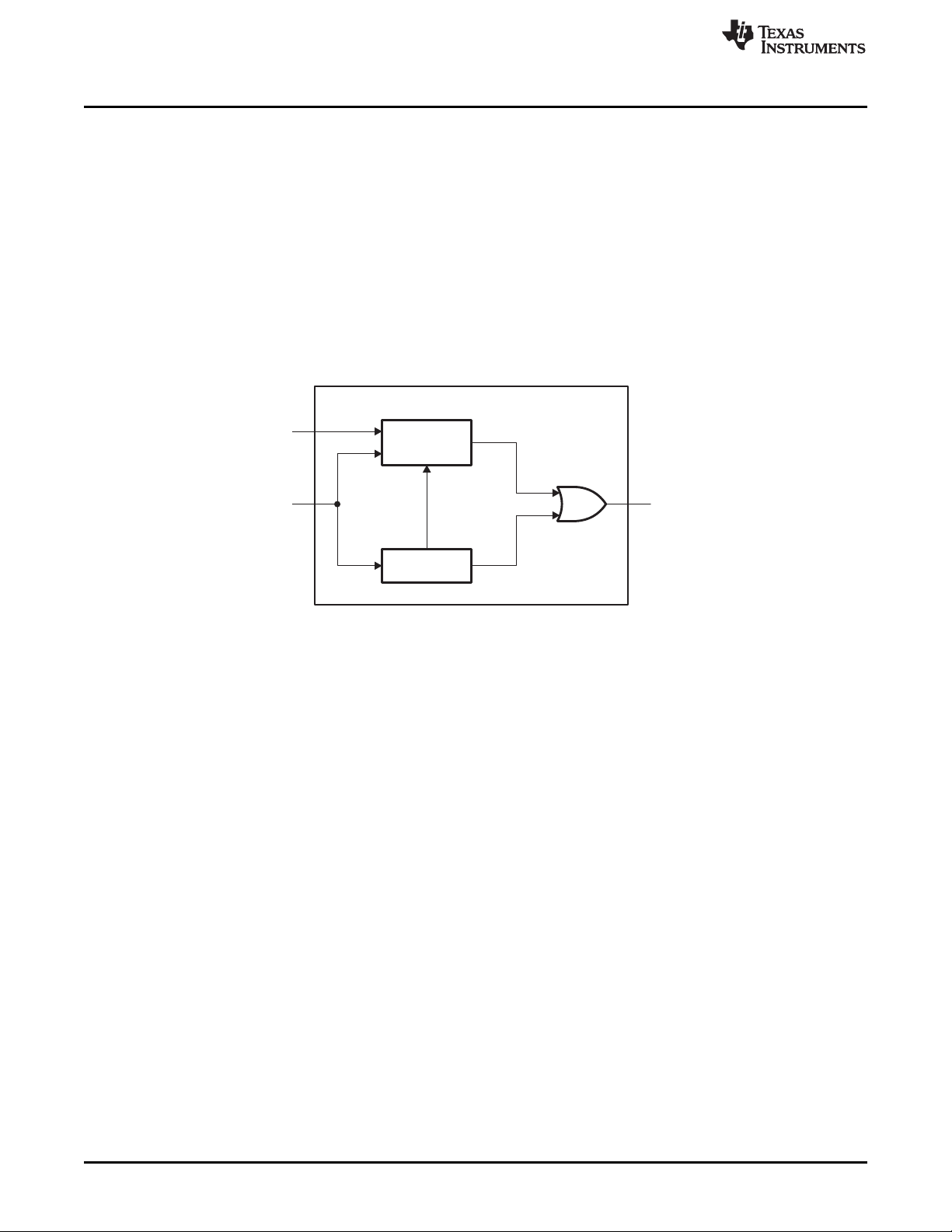
Pacingblock
Timed-
delaySM
DIV_NEXT
DivideSM
EVT_TIMED
EVT_DIV
EVT_OUT
PS_TICK
EVT_IN
EMAC Functional Architecture
2.7.1 Pacing Block
In simple terms, interrupt pacing represents delaying the initial EMAC events to CPU interrupt based on
certain criteria. The pacing block is the basic building block for the interrupt pacing operation. One of the
motivations for interrupt pacing is that during Ethernet operation, hundreds or thousands of interrupts are
generated per second for packets transmitted or received and interrupt pacing relieves the CPU of the
burden of processing every single interrupt. This block provides time-based or count-based pacing of
interrupts, in any combination. In addition, this block supports reprogramming of timer value and count
value without hardware/software race condition and also facilitates use of the same timer and count
values for the next event period.
The EVT_IN is the pulse interrupt from EMAC. This is forwarded to timed-delay and divide by N state
machines (see Figure 15). The state machine outputs are combined and sent out as EVT_OUT. PS_TICK
is the clock tick from the prescalar block. The prescaler block forwards this signal to all the pacing blocks.
www.ti.com
Figure 15. Pacing Block
42
C6472/TCI6486 EMAC/MDIO SPRUEF8F–March 2006–Revised November 2010
Submit Documentation Feedback
Copyright © 2006–2010, Texas Instruments Incorporated
Page 43

Waiting
Delay
Time=0
Time=0
Output
EVT_PULSE=0 &&
DIV_NEXT=1
EVT_PULSE=1&&
TIME< TIME_CFG
EVT_PULSE=1&&
DIV_NEXT=1
PS_TICK=1&&
TIME< TIME_CFG
&&DIV_NEXT=0
EVT_PULSE=1 &&
TIME < TIME_CFG
EVT_PULSE=0(or)
EVT_PULSE=1&& TIME>= TIME_CFG
Increment
time
Time=0
PS_TICK=0&&
DIV_NEXT=0
PS_TICK=1&&
TIME>= TIME_CFG
Time=0
Time=0
EVT_PULSE=0(or)
EVT_PULSE=1&& TIME>= TIME_CFG
www.ti.com
2.7.2 Timed Delay State Machine (TDSM)
The timed-delay state machine fully implements the functionality of the time-delay based interrupt pacing.
The TIME_CFG bit field of the TPCFG and RPCFG registers (described in Section 3) is set to 0 on reset
and disables this state machine. When the TIME_CFG is set to a non-zero value, an output pulse is
generated after the TIME_CFG number of prescalar output periods. The counter starts counting on the
first event.
The state machine has three states, WAITING, DELAY, and OUTPUT. Upon reset, the state machine is
placed in the WAITING state. The state machine makes transitions between the states as shown in
Figure 16. Note that states that are grayed out are transitional states, in the sense that the SM does not
stay in the grayed state. While in the transitional state, it typically does an operation, like incrementing the
TIME or resetting the TIME. It then changes the state to the state illustrated by the dotted line.
Figure 16. TDSM State Transition Diagram
EMAC Functional Architecture
SPRUEF8F–March 2006–Revised November 2010 C6472/TCI6486 EMAC/MDIO
Submit Documentation Feedback
Copyright © 2006–2010, Texas Instruments Incorporated
43
Page 44

Waiting
Count
Output
EVT_PULSE=0(or)EVT_PULSE=1&&
CNT >=CNT_CFG&& TIME_CFGI=0
Increment
CNT
CNT=1
EVT_PULSE=0
&&CR=0
EVT_PULSE=0
&& CR=1
EVT_PULSE=1 &&
CNT < CNT_CFG &&
CR=0
EVT_PULSE=1 &&
CNT < CNT_CFG
CNT=1
NEXT_
DIV=1
CNT=1
EVT_PULSE=1&&
CR=1&&CNT <
CNT_CFG
EVT_PULSE=1 && CNT >=
CNT_CFG && TIME_CFG==0
NEXT_
DIV=1
CNT >=CNT_CFG
&&EVT_PULSE=1
EVT_PULSE=1&&
CNT <CNT_CFG
EVT_PULSE=0 (or)
CNT >= CNT_CFG
EMAC Functional Architecture
2.7.3 Divide-by-N State Machine (DSM)
The divide-by-N state machine fully implements the functionality of the count-based interrupt pacing. The
CNT_CFG bit field of the TPCFG and RPCFG registers (described in Section 3) is set to 0 on reset and
immediately generates a pulse (basically means a zero delay), when the TIME_CFG is also set to 0 (i.e.,
timed-delay SM is disabled). When the TIME_CFG is set to non-zero, it then disables the divide-by-N
state machine. When the CNT_CFG is set to non-zero, the CNT_CFG number of events are counted
before an output pulse is generated. The counter resets (and reloads) every time when a divide-by-N
pulse is generated.
The state machine has three states, WAITING, COUNT, and OUTPUT. Upon reset, the state machine is
placed in the WAITING state. The state machine makes transitions between the states as shown in
Figure 17. Note that states that are grayed out are transitional states, in the sense that the SM does not
stay in the grayed state. While in the transitional state, it typically does an operation, like setting the
counter to a certain value.
Figure 17. DSM State Transition Diagram
www.ti.com
44
C6472/TCI6486 EMAC/MDIO SPRUEF8F–March 2006–Revised November 2010
Copyright © 2006–2010, Texas Instruments Incorporated
Submit Documentation Feedback
Page 45

PacingblockTXEVT[0]
PacingblockTXEVT[1]
EW_INTCTL[8]
EW_INTCTL[9]
PacingblockTXEVT[2]
PacingblockTXEVT[3]
EW_INTCTL[10]
EW_INTCTL[11]
PacingblockTXEVT[4]
PacingblockTXEVT[5]
EW_INTCTL[12]
EW_INTCTL[13]
Pacingblock
TXEVT[6]
PacingblockTXEVT[7]
EW_INTCTL[14]
EW_INTCTL[15]
PS_TICK EW_INTCTL[15:8]
MACTXINT
Transmitpacerandinterruptcombiner
www.ti.com
2.7.4 Transmit Pacer and Interrupt Combiner (TPIC)
The transmit pacer and interrupt combiner (TPIC) block performs the following functions:
• Optionally implements pacing for transmit events.
• Combines the output of the pacer module based on the settings of the bits 8 to 15 in the EW_INTCTL
register and generates a single MACTXINT interrupt per the C64x+ megamodule.
• Receives a single PS_TICK and forwards it to all the pacing blocks.
• Allows, per interrupt enabling or disabling of the interrupts, the setting of bits 8 to 15 in the
EW_INTCTL register.
Figure 18 shows the block diagram of transmit pacer and interrupt combiner (TPIC). TXEVT is an interrupt
from EMAC.
Figure 18. Transmit Pacer and Interrupt Combiner
EMAC Functional Architecture
SPRUEF8F–March 2006–Revised November 2010 C6472/TCI6486 EMAC/MDIO
Submit Documentation Feedback
Copyright © 2006–2010, Texas Instruments Incorporated
45
Page 46
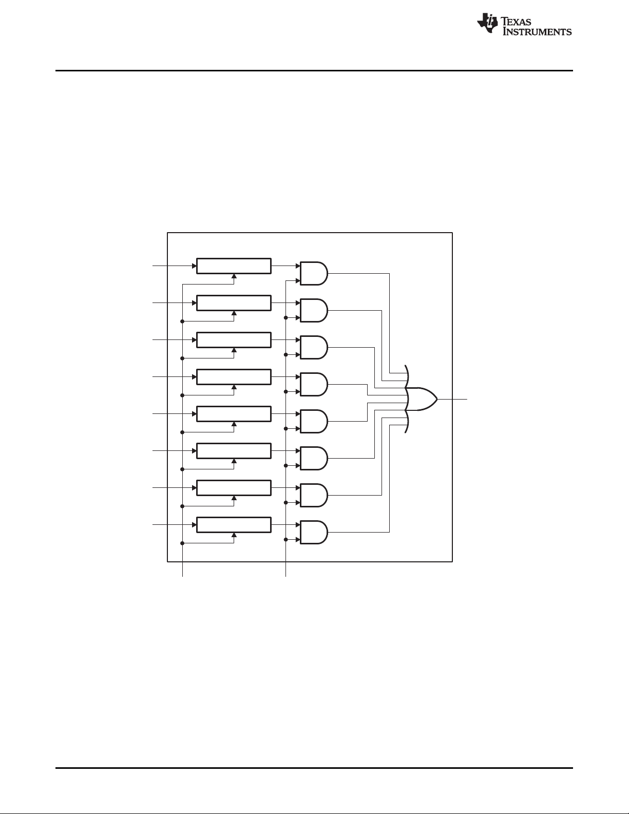
PacingblockRXEVT[0]
PacingblockRXEVT[1]
EW_INTCTL[16]
EW_INTCTL[17]
PacingblockRXEVT[2]
PacingblockRXEVT[3]
EW_INTCTL[18]
EW_INTCTL[19]
PacingblockRXEVT[4]
PacingblockRXEVT[5]
EW_INTCTL[20]
EW_INTCTL[21]
Pacingblock
RXEVT[6]
PacingblockRXEVT[7]
EW_INTCTL[22]
EW_INTCTL[23]
PS_TICK EW_INTCTL[23:16]
MACRXINT
Receivepacerandinterruptcombiner
EMAC Functional Architecture
2.7.5 Receive Pacer and Interrupt Combiner (RPIC)
The receive pacer and interrupt combiner (RPIC) block performs following functions:
• Implements pacing for receive events.
• Combines the output of the pacer module based on the settings of bits 16 to 23 in the EW_INTCTL
register and generates a single MACRXINT interrupt per the C64x+ megamodule.
• Receives a single PS_TICK and forwards it to all the pacing blocks.
• Allows, per interrupt enabling or disabling of the interrupts, the setting of bits 16 to 23 in the
EW_INTCTL register.
Figure 19 shows the block diagram of receive pacer and interrupt combiner (RPIC).
Figure 19. Receive Pacer and Interrupt Combiner
www.ti.com
46
C6472/TCI6486 EMAC/MDIO SPRUEF8F–March 2006–Revised November 2010
Copyright © 2006–2010, Texas Instruments Incorporated
Submit Documentation Feedback
Page 47

EW_INTCTL[1]
EW_INTCTL[2]
EW_INTCTL[3]
EW_INTCTL[4]
EW_INTCTL[4:1]
MACINT
Commoninterruptcombinerblock
HOST
STAT
MDIO_LINT
MDIO_USER
www.ti.com
2.7.6 Common Interrupt Combiner (CIC)
The common interrupt combiner (CIC) block performs following functions:
• Combines the two common interrupts from EMAC (HOST and STAT) with the two MDIO interrupts
(MDIO_LINT and MDIO_USER) and generates a single MACINT interrupt per theC64x+ megamodule.
• Performs a level-to-pulse conversion of the interrupts because the interrupts from EMAC and MDIO
are level sensitive and the C64x+ megamodule expects a pulse interrupt.
• Allows, per interrupt enabling or disabling of the interrupts, the setting of bits 1 to 4 in the EW_INTCTL
register.
Figure 20 is the block diagram representing common interrupt combiner.
Figure 20. Common Interrupt Combiner
EMAC Functional Architecture
2.8 Management Data Input/Output (MDIO) Module
The Management Data Input/Output (MDIO) module manages up to 32 physical layer (PHY) devices
connected to the Ethernet Media Access Controller (EMAC). The MDIO module allows almost transparent
operation of the MDIO interface with little maintenance from the CPU.
The MDIO module enumerates all PHY devices in the system by continuously polling 32 MDIO addresses.
Once it detects a PHY device, the MDIO module reads the PHY status register to monitor the PHY link
state. The MDIO module stores link change events that can interrupt the CPU. The event storage allows
the CPU to poll the link status of the PHY device without continuously performing MDIO module accesses.
However, when the system must access the MDIO module for configuration and negotiation, the MDIO
module performs the MDIO read or write operation independent of the CPU. This independent operation
allows the DSP to poll for completion or interrupt the CPU once the operation has completed.
2.8.1 MDIO Module Components
The MDIO module (shown in Figure 21) interfaces to PHY components through two MDIO pins (MDCLK
and MDIO), and to the DSP core through the EMIC module and the configuration bus. The MDIO module
consists of the following logical components:
• MDIO clock generator
• Global PHY detection and link state monitoring
• Active PHY monitoring
• PHY register user access
SPRUEF8F–March 2006–Revised November 2010 C6472/TCI6486 EMAC/MDIO
Submit Documentation Feedback
Copyright © 2006–2010, Texas Instruments Incorporated
47
Page 48

EMIC
module
Control
registers
andlogic
PHY
monitoring
Peripheral
clock
MDIO
clock
generator
USERINT
MDIO
interface
PHY
polling
MDCLK
MDIO
LINKINT
Configurationbus
EMAC Functional Architecture
2.8.1.1 MDIO Clock Generator
The MDIO clock generator controls the MDIO clock based on a divide-down of the peripheral clock
(CPUCLK/6). The MDIO clock is specified to run up to 2.5 MHz, although typical operation would be 1.0
MHz. As the peripheral clock frequency is variable (CPUclk/6), the application software or driver controls
the divide-down amount.
www.ti.com
Figure 21. MDIO Module Block Diagram
2.8.1.2 Global PHY Detection and Link State Monitoring
The MDIO module enumerates all PHY devices in the system by continuously polling all 32 MDIO
addresses. The module tracks whether a PHY on a particular address has responded, and whether the
PHY currently has a link. This information allows the software application to quickly determine which
MDIO address the PHY is using, and if the system is using more than one PHY. The software application
can then quickly switch between PHYs based on their current link status.
2.8.1.3 Active PHY Monitoring
Once a PHY candidate has been selected for use, the MDIO module transparently monitors its link state
by reading the PHY status register. The MDIO device stores link change events that may optionally
interrupt the CPU. Thus, the system can poll the link status of the PHY device without continuously
performing MDIO accesses. Up to two PHY devices can be actively monitored at any given time.
2.8.1.4 PHY Register User Access
When the DSP must access the MDIO for configuration and negotiation, the PHY access module performs
the actual MDIO read or write operation independent of the CPU. Thus, the CPU can poll for completion
or receive an interrupt when the read or write operation has been performed. There are two user access
registers (USERACCESS0 and USERACCESS1), allowing the software to submit up to two access
requests simultaneously. The requests are processed sequentially.
48
C6472/TCI6486 EMAC/MDIO SPRUEF8F–March 2006–Revised November 2010
Submit Documentation Feedback
Copyright © 2006–2010, Texas Instruments Incorporated
Page 49

www.ti.com
2.8.2 MDIO Module Operational Overview
The MDIO module implements the 802.3 serial management interface to simultaneously interrogate and
control up to two Ethernet PHYs, using a shared two-wired bus. It separately performs auto-detection and
records the current link status of up to 32 PHYs, polling all 32 MDIO addresses.
Application software uses the MDIO module to configure the auto-negotiation parameters of the primary
PHY attached to the EMAC, retrieve the negotiation results, and configure required parameters in the
EMAC. Up to two Ethernet PHYs can be directly controlled and queried. The Media Independent Interface
addresses of these two PHY devices are specified in the PHYADRMON fields of the USERPHYSELn
register. The module can be programmed to trigger a CPU interrupt on a PHY link change event by setting
the LINKINTENB bit in USERPHYSELn. Reads and writes to registers in these PHY devices are
performed using the USERACCESSn register.
The MDIO module powers up in an idle state until it is enabled by setting the ENABLE bit in the
CONTROL register. This also configures the MDIO clock divider and preamble mode selection. The MDIO
preamble is enabled by default, but it can be disabled if none of the connected PHYs require it.
Once the MDIO module is enabled, the MDIO interface state machine continuously polls the PHY link
status (by reading the generic PHY Status register) of all possible 32 PHY addresses and records the
results in the ALIVE and LINK registers. The corresponding bit for each PHY (0-31) is set in the ALIVE
register if the PHY responded to the read request. The corresponding bit is set in the LINK register if the
PHY responded and also is currently linked. In addition, any PHY register read transactions initiated by
the application software using the USERACCESSn register cause the ALIVE register to be updated.
The USERPHYSELn register is used to track the link status of any two of the 32 possible PHY addresses.
Changes in the link status of the two monitored PHYs sets the appropriate bit in the LINKINTRAW and
LINKINTMASKED registers, if they are enabled by the LINKINTENB bit in USERPHYSELn.
While the MDIO module is enabled, the host can issue a read or write transaction over the management
interface using the DATA, PHYADR, REGADR, and WRITE bits in the USERACCESSn register. When
the application sets the GO bit in USERACCESSn, the MDIO module begins the transaction without any
further intervention from the CPU. Upon completion, the MDIO module clears the GO bit and sets the
USERINTRAW[0-1] bit in the USERINTRAW register corresponding to the USERACCESSn used. The
corresponding USERINTMASKED bit in the USERINTMASKED register may also be set, depending on
the mask setting configured in the USERINTMASKSET and USERINTMASKCLEAR registers.
A round-robin arbitration scheme schedules transactions that may be queued using both USERACCESS0
and USERACCESS1. The application software must verify the status of the GO bit in USERACCESSn
before initiating a new transaction to ensure that the previous transaction has completed. The application
software can use the ACK bit in USERACCESSn to determine the status of a read transaction.
EMAC Functional Architecture
2.8.2.1 Initializing the MDIO Module
To have the application software or device driver initialize the MDIO device, perform the following:
1. Configure the PREAMBLE and CLKDIV bits in the CONTROL register.
2. Enable the MDIO module by setting the ENABLE bit in the CONTROL register.
3. The ALIVE register can be read after a delay to determine which PHYs responded, and the LINK
register can determine which of those (if any) already have a link.
4. Set up the appropriate PHY addresses in the USERPHYSELn register, and set the LINKINTENB bit to
enable a link change event interrupt if desirable.
5. If an interrupt on a general MDIO register access is desired, set the corresponding bit in the
USERINTMASKSET register to use the USERACCESSn register. If only one PHY is to be used, the
application software can set up one of the USERACCESSn registers to trigger a completion interrupt.
The other register is not set up.
SPRUEF8F–March 2006–Revised November 2010 C6472/TCI6486 EMAC/MDIO
Submit Documentation Feedback
Copyright © 2006–2010, Texas Instruments Incorporated
49
Page 50

EMAC Functional Architecture
2.8.2.2 Writing Data to a PHY Register
The MDIO module includes a user access register (USERACCESSn) to directly access a specified PHY
device. To write a PHY register, perform the following:
1. Ensure that the GO bit in the USERACCESSn register is cleared.
2. Write to the GO, WRITE, REGADR, PHYADR, and DATA bits in USERACCESSn corresponding to the
desired PHY and PHY register.
3. The write operation to the PHY is scheduled and completed by the MDIO module. Completion of the
write operation can be determined by polling the GO bit in USERACCESSn for a 0.
4. Completion of the operation sets the corresponding bit in the USERINTRAW register for the
USERACCESSn used. If interrupts have been enabled on this bit using the USERINTMASKSET
register, then the bit is also set in the USERINTMASKED register and an interrupt is triggered on the
DSP.
2.8.2.3 Reading Data From a PHY Register
The MDIO module includes a user access register (USERACCESSn) to directly access a specified PHY
device. To read a PHY register, perform the following:
1. Ensure that the GO bit in the USERACCESSn register is cleared.
2. Write to the GO, REGADR, and PHYADR bits in USERACCESSn corresponding to the desired PHY
and PHY register.
3. The read data value is available in the DATA bits of USERACCESSn after the module completes the
read operation on the serial bus. Completion of the read operation can be determined by polling the
GO and ACK bits in USERACCESSn. Once the GO bit has cleared, the ACK bit is set on a successful
read.
4. Completion of the operation sets the corresponding bit in the USERINTRAW register for the
USERACCESSn used. If interrupts have been enabled on this bit using the USERINTMASKSET
register, then the bit is also set in the USERINTMASKED register and an interrupt is triggered on the
DSP.
www.ti.com
2.8.2.4 Example of MDIO Register Access Code
The MDIO module uses the USERACCESSn register to access the PHY control registers. Software
functions that implement the access process include the following four macros:
PHYREG_read (regadr, phyadr ) Starts the process of reading a PHY register
PHYREG_write(regadr, phyadr, data ) Starts the process of writing a PHY register
PHYREG_wait ( ) Synchronizes operation (makes sure read/write is idle)
PHYREG_wait Results (results ) Waits for read to complete and returns data read
It is not necessary to wait after a write operation, as long as the status is checked before every operation
to make sure the MDIO hardware is idle. An alternative approach is to call PHYREG_wait () after every
write, and PHYREG_wait Results () after every read, then the hardware can be assumed to be idle when
starting a new operation.
50
C6472/TCI6486 EMAC/MDIO SPRUEF8F–March 2006–Revised November 2010
Submit Documentation Feedback
Copyright © 2006–2010, Texas Instruments Incorporated
Page 51

www.ti.com
The implementation of these macros using the register layer Chip Support Library (CSL) is shown in
Example 3 (USERACCESS0 is assumed).
Note that this implementation does not check the ACK bit on PHY register reads; in other words, it does
not follow the procedure outlined in Section 2.8.2.3. As the ALIVE register initially selects a PHY, it is
assumed that the PHY is acknowledging read operations. It is possible that a PHY could become inactive
at a future point in time. For example, a PHY can have its MDIO addresses changed while the system is
running, although it is not a common occurrence. This condition can be tested by periodically checking the
PHY state in the ALIVE register.
Example 3. MDIO Register Access Macros
EMAC Functional Architecture
#define PHYREG_read(regadr, phyadr) \
#define PHYREG_write(regadr, phyadr, data) \
#define PHYREG_wait() \
#define PHYREG_wait Results(results ) { \
MDIO_REGS->USERACCESS0 = \
CSL_FMK(MDIO_USERACCESS0_GO,1u) | \
CSL_FMK(MDIO_USERACCESS0_REGADR,regadr) | \
CSL_FMK(MDIO_USERACCESS0_PHYADR,phyadr)
MDIO_REGS->USERACCESS0 = \
CSL_FMK(MDIO_USERACCESS0_GO,1u) | \
CSL_FMK(MDIO_USERACCESS0_WRITE,1) | \
CSL_FMK(MDIO_USERACCESS0_REGADR,regadr) | \
CSL_FMK(MDIO_USERACCESS0_PHYADR,phyadr) | \
CSL_FMK(MDIO_USERACCESS0_DATA, data)
while (CSL_FEXT(MDIO_REGS->USERACCESS0,MDIO_USERACCESS0_GO) )
while (CSL_FEXT(MDIO_REGS->USERACCESS0,MDIO_USERACCESS0_GO) ); \
results = CSL_FEXT(MDIO_REGS->USERACCESS0, MDIO_USERACCESS0_DATA); }
SPRUEF8F–March 2006–Revised November 2010 C6472/TCI6486 EMAC/MDIO
Submit Documentation Feedback
Copyright © 2006–2010, Texas Instruments Incorporated
51
Page 52

Clockand
resetlogic
Receive
DMA engine
Interrupt
controller
Transmit
DMA engine
Control
registers
EMIC
Receive
FIFO
MAC
receiver
State
RAM
Statistics
Transmit
FIFO
MAC
transmitter
Receive
address
SYNC
RMII0,RMII1
RGMII0,RGMII1
MII0/GMII0
S3MII0,S3MII1
Configurationbus
CPPI
buffer
manager
Configurationbus
EMAC Functional Architecture
2.9 EMAC Module
This section discusses the architecture and basic functions of the EMAC sub-module integrated with the
TCI6486/C6472 device.
2.9.1 EMAC Module Components
There are two EMAC modules integrated with the TCI6486/C6472 device. EMAC0 interfaces with PHY
through one of five interfaces: MII, GMII, S3MII, RMII, or RGMII. EMAC1 interfaces with PHY through one
of three interfaces: S3MII, RMII, or RGMII. In Figure 22, the number associated with each MII interface
shows the EMAC module with which the interface is available. For example: RMII0 is EMAC0 interface,
RMII1 is EMAC1 interface.
Figure 22. EMAC Module Block Diagram
www.ti.com
52
Each EMAC peripheral used has the following components:
• The receive path:
– Receive DMA engine
The receive DMA engine performs the data transfer between the receive FIFO and the device
internal or external memory. It interfaces to the processor through the bus arbiter in the CPPI buffer
manager. This DMA engine is totally independent of the TCI6486/C6472 DSP EDMA.
– Receive FIFO
The receive FIFO consists of 68 cells of 64 bytes each and the associated control logic. The FIFO
buffers receive data in preparation for writing into packet buffers in device memory and also enable
receive FIFO flow control.
– MAC receiver
The MAC receiver detects and processes incoming network frames, de-frames them, and places
them into the receive FIFO. The MAC receiver also detects errors and passes statistics to the
statistics RAM.
– Receive address sub-module
The receive address sub-module performs address matching and address filtering based on the
incoming packet's destination address. It contains a 32 x 53 bit two-port RAM in which up to 32
addresses can be stored to be either matched or filtered by the EMAC.
The RAM may contain multicast packet addresses, but the associated channel must have the
unicast enable bit set, even though it is a multicast address. The unicast enable bits are used with
multicast addresses in the receive address RAM (not the multicast hash enable bits). Therefore,
hash matches can be disabled, but specific multicast addresses can be matched (or filtered) in the
RAM. If a multicast packet hash matches, the packet may still be filtered in the RAM. Each packet
C6472/TCI6486 EMAC/MDIO SPRUEF8F–March 2006–Revised November 2010
Copyright © 2006–2010, Texas Instruments Incorporated
Submit Documentation Feedback
Page 53

www.ti.com
• The transmit path:
• Statistics logic
• State RAM
• Interrupt controller
• Control registers and logic
• Clock and reset logic
EMAC Functional Architecture
can be sent to only a single channel.
– Transmit DMA engine
The transmit DMA engine performs the data transfer between the device internal or external
memory and the transmit FIFO. It interfaces to the processor through the bus arbiter in the CPPI
buffer manager. This DMA engine is totally independent of the TCI6486/C6472 DSP EDMA.
– Transmit FIFO
The transmit FIFO consists of 24 cells of 64 bytes each and the associated control logic. This
enables a packet of 1518 bytes (standard Ethernet packet size) to be sent without the possibility of
under-run. The FIFO buffers data in preparation for transmission.
– MAC transmitter
The MAC transmitter formats frame data from the transmit FIFO and transmits the data using the
CSMA/CD access protocol. The frame CRC can be automatically appended, if required. The MAC
transmitter also detects transmission errors and passes statistics to the statistics registers.
The statistics logic RAM counts and stores the Ethernet statistics, keeping track of 36 different
Ethernet packet statistics.
The state RAM contains the head descriptor pointers and completion pointers registers for both
transmit and receive channels.
The interrupt controller contains the interrupt-related registers and logic. The 18 raw EMAC interrupts
are input to this sub-module and masked module interrupts are output.
The EMAC is controlled by a set of memory-mapped registers. The control logic also signals transmit,
receive, and status related interrupts to the CPU through the EMIC module.
The clock and reset sub-module generates all the clocks and resets for the EMAC peripheral.
2.9.2 EMAC Module Operational Overview
After reset, initialization, and configuration of the EMAC, the application software running on the host may
initiate transmit operations. Transmit operations are initiated by host writes to the appropriate transmit
channel head descriptor pointer contained in the state RAM block. The transmit DMA controller then
fetches the first packet in the packet chain from memory. The DMA controller writes the packet into the
transmit FIFO in bursts of 64-byte cells. The MAC transmitter initiates the packet transmission when either
the threshold number of cells (configurable via TXCELLTHRESH in the FIFOCONTROL register) have
been written to the transmit FIFO, or a complete packet has been written, whichever is smaller. The SYNC
block transmits the packet over one of the MII interfaces in accordance with the 802.3 protocol. The
statistics block counts transmit statistics.
Receive operations are initiated by host writes to the appropriate receive channel head descriptor pointer
after host initialization and configuration. The SYNC sub-module receives packets and strips off the
Ethernet related protocol. The packet data is input to the MAC receiver, which checks for address match
(in conjunction with the receive address block) and processes errors. Accepted packets are written to the
receive FIFO in bursts of 64-byte cells. The receive DMA controller then writes the packet data to memory.
The statistics block counts receive statistics.
The EMAC module operates independently of the CPU. It is configured and controlled by its register set
mapped into device memory. Information about data packets is communicated using 16-byte descriptors.
For transmit operations, each 16-byte descriptor describes a packet or packet fragment in the system's
internal or external memory. For receive operations, each 16-byte descriptor represents a free packet
buffer or buffer fragment. On both transmit and receive, an Ethernet packet is allowed to span one or
more memory fragments, represented by one 16-byte descriptor per fragment. In typical operation, there is
only one descriptor per receive buffer, but transmit packets may be fragmented, depending on the
software architecture.
SPRUEF8F–March 2006–Revised November 2010 C6472/TCI6486 EMAC/MDIO
Submit Documentation Feedback
Copyright © 2006–2010, Texas Instruments Incorporated
53
Page 54

EMAC Functional Architecture
An interrupt is issued to the CPU whenever a transmit or receive operation has completed. However, it is
not necessary for the CPU to service the interrupt while there are additional resources available. In other
words, the EMAC continues to receive Ethernet packets until its receive descriptor list has been
exhausted. On transmit operations, the transmit descriptors need only be serviced to recover their
associated memory buffer. Thus, it is possible to delay servicing of the EMAC interrupt if there are
real-time tasks to perform.
Eight channels are supplied for both transmit and receive operations. On transmit, the eight channels
represent eight independent transmit queues. The EMAC can be configured to treat these channels as an
equal priority round-robin queue, or as a set of eight fixed-priority queues. On receive, the eight channels
represent eight independent receive queues with packet classification. Packets are classified based on the
destination MAC address. Each of the eight channels is assigned its own MAC address, enabling the
EMAC module to act like eight virtual MAC adapters. Also, specific types of frames can be sent to specific
channels. For example, multicast, broadcast, or other (promiscuous, error, etc.) frames can each be
received on a specific receive channel queue.
The EMAC tracks 36 different statistics, as well as recording the status of each individual packet in its
corresponding packet descriptor.
2.10 Media Independent Interfaces
The EMAC0 supports MII, GMII, RMII, S3MII and RGMII physical interfaces to external PHY devices,
whereas the EMAC1 supports RMII, S3MII and RGMII interfaces.
The following sections discuss the operation of these interfaces in 10/100 Mbps mode (MII, RMII, GMII
and RGMII), and 1000 Mbps mode (GMII and RGMII). An IEEE 802.3 compliant Ethernet MAC controls
these interfaces.
www.ti.com
2.10.1 Data Reception
2.10.1.1 Receive Control
Data received from the PHY is interpreted and output to the EMAC receive FIFO. Interpretation involves
detection and removal of the preamble and start-of-frame delimiter, extraction of the address and frame
length, data handling, error checking and reporting, cyclic redundancy checking (CRC), and statistics
control signal generation. Receive address detection and frame filtering of the frames that do not
address-match is performed outside the Media Independent interface.
2.10.1.2 Receive Inter-Frame Interval
The 802.3 required inter-packet gap (IPG) is 24 receive data clocks (96 bit times). However, the EMAC
can tolerate a reduced IPG (2 receive clocks in 10/100 Mbps mode and 5 receive clocks in 1000 Mbps
mode) with a correct preamble and start frame delimiter. This interval between frames must comprise (in
the following order):
1. An Inter-Packet Gap (IPG).
2. A seven bytes preamble (all bytes 55h).
3. A one byte start-of-frame delimiter (5Dh).
2.10.1.3 Receive Flow Control
When enabled and triggered, receive flow control is initiated to limit the EMAC from further frame
reception. Two forms of receive flow control are implemented on the TCI6486/C6472 device:
• Receive buffer flow control
• Receive FIFO flow control
When enabled and triggered, receive buffer flow control prevents further frame reception based on the
number of free buffers available. Receive buffer flow control issues flow control collisions in half-duplex
mode and IEEE 802.3X pause frames for full-duplex mode.
54
C6472/TCI6486 EMAC/MDIO SPRUEF8F–March 2006–Revised November 2010
Submit Documentation Feedback
Copyright © 2006–2010, Texas Instruments Incorporated
Page 55

www.ti.com
Receive buffer flow control is triggered when the number of free buffers in any enabled receive channel
(RXnFREEBUFFER) is less than or equal to the channel flow control threshold register
(RXnFLOWTHRESH) value. Receive flow control is independent of receive QOS, except that both use the
free buffer values.
When enabled and triggered, receive FIFO flow control prevents further frame reception based on the
number of cells currently in the receive FIFO. Receive FIFO flow control may be enabled only in
full-duplex mode (FULLDUPLEX bit is set in the MACCONTROL register). Receive flow control prevents
reception of frames on the port until all of the triggering conditions clear, at which time frames may again
be received by the port.
Receive FIFO flow control is triggered when the occupancy of the FIFO is greater than or equal to the
RXFIFOFLOWTHRESH value in the FIFOCONTROL register. The RXFIFOFLOWTHRESH value must be
greater than or equal to 1h and less than or equal to 42h (decimal 66). The RXFIFOFLOWTHRESH reset
value is 2h.
Receive flow control is enabled by the RXBUFFERFLOWEN bit and the RXFIFOFLOWEN bit in the
MACCONTROL register. The FULLDUPLEX bit in the MACCONTROL register configures the EMAC for
collision or IEEE 802.3X flow control.
2.10.1.4 Collision-Based Receive Buffer Flow Control
Collision-based receive buffer flow control provides a means of preventing frame reception when the
EMAC is operating in half-duplex mode (FULLDUPLEX bit is cleared in MACCONTROL register). When
receive flow control is enabled and triggered, the EMAC generates collisions for received frames. The jam
sequence transmitted is the 12-byte sequence C3.C3.C3.C3.C3.C3.C3.C3.C3.C3.C3.C3 in hexadecimal.
The jam sequence begins approximately when the source address starts to be received. These forced
collisions are not limited to a maximum of 16 consecutive collisions and are independent of the normal
back-off algorithm.
Receive flow control does not depend on the value of the incoming frame destination address. A collision
is generated for any incoming packet, regardless of the destination address, if any EMAC enabled
channel's free buffer register value is less than or equal to the channel's flow threshold value.
EMAC Functional Architecture
2.10.1.5 IEEE 802.3X Based Receive Buffer Flow Control
IEEE 802.3x based receive buffer flow control provides a means of preventing frame reception when the
EMAC is operating in full-duplex mode (the FULLDUPLEX bit is set in the MACCONTROL register). When
receive flow control is enabled and triggered, the EMAC transmits a pause frame to request that the
sending station stop transmitting for the period indicated within the transmitted pause frame.
The EMAC transmits a pause frame to the reserved multicast address at the first available opportunity
(immediately if currently idle, or following the completion of the frame currently being transmitted). The
pause frame contains the maximum possible value for the pause time (FFFFh). The EMAC counts the
receive pause frame time (decrements FF00h to 0) and retransmits an outgoing pause frame, if the count
reaches zero. When the flow control request is removed, the EMAC transmits a pause frame with a zero
pause time to cancel the pause request.
Note that transmitted pause frames are only a request to the other end station to stop transmitting.
Frames that are received during the pause interval are received normally (provided the receive FIFO is not
full).
Pause frames are transmitted if enabled and triggered, regardless of whether or not the EMAC is
observing the pause time period from an incoming pause frame.
The EMAC transmits pause frames as described below:
• The 48-bit reserved multicast destination address 01.80.C2.00.00.01h.
• The 48-bit source address (set via the MACSRCADDRLO and MACSRCADDRHI registers).
• The 16-bit length/type field containing the value 88.08h.
• The 16-bit pause opcode equal to 00.01h.
• The 16-bit pause time value of FF.FFh. A pause-quantum is 512 bit-times. Pause frames sent to
cancel a pause request have a pause time value of 00.00h.
SPRUEF8F–March 2006–Revised November 2010 C6472/TCI6486 EMAC/MDIO
Submit Documentation Feedback
Copyright © 2006–2010, Texas Instruments Incorporated
55
Page 56

EMAC Functional Architecture
• Zero padding to 64-byte data length (EMAC transmits only 64-byte pause frames).
• The 32-bit frame-check sequence (CRC word).
All quantities are hexadecimal and are transmitted most-significant-byte first. The least-significant-bit
(LSB) is transferred first in each byte.
If the RXBUFFERFLOWEN bit in the MACCONTROL register is cleared while the pause time is nonzero,
then the pause time is cleared and a zero count pause frame is sent.
2.10.2 Data Transmission
The EMAC passes data to the PHY from the transmit FIFO (when enabled). Data is synchronized to the
transmit clock rate. Transmission begins when there are TXCELLTHRESH cells of 64 bytes each, or a
complete packet, in the FIFO.
2.10.2.1 Transmit Control
A jam sequence is output if a collision is detected on a transmit packet. If the collision was late (after the
first 64 bytes have been transmitted), the collision is ignored. If the collision is not late, the controller will
back off before retrying the frame transmission. When operating in full-duplex mode, the carrier sense
(MCRS) and collision-sensing (MCOL) modes are disabled.
2.10.2.2 CRC Insertion
If the SOP buffer descriptor PASSCRC flag is cleared, the EMAC generates and appends a 32-bit
Ethernet CRC onto the transmitted data. For the EMAC-generated CRC case, a CRC (or placeholder) at
the end of the data is allowed but not required. The buffer byte count value should not include the CRC
bytes, if they are present.
If the SOP buffer descriptor PASSCRC flag is set, then the last four bytes of the transmit data are
transmitted as the frame CRC. The four CRC data bytes should be the last four bytes of the frame and
should be included in the buffer byte count value. The MAC performs no error checking on the outgoing
CRC.
www.ti.com
2.10.2.3 Adaptive Performance Optimization (APO)
The EMAC incorporates adaptive performance optimization (APO) logic that may be enabled by setting
the TXPACE bit in the MACCONTROL register. Transmission pacing to enhance performance is enabled
when the TXPACE bit is set. Adaptive performance pacing introduces delays into the normal transmission
of frames, delaying transmission attempts between stations, and reducing the probability of collisions
occurring during heavy traffic (as indicated by frame deferrals and collisions). These actions increase the
chance of a successful transmission.
When a frame is deferred, suffers a single collision, multiple collisions, or excessive collisions, the pacing
counter is loaded with an initial value of 31. When a frame is transmitted successfully (without
experiencing a deferral, single collision, multiple collision, or excessive collision), the pacing counter is
decremented by 1 down to 0.
If the pacing counter is zero, this allows a new frame to immediately attempt transmission (after one IPG).
If the pacing counter is nonzero, the frame is delayed by a pacing delay of approximately four inter-packet
gap delays. APO only affects the IPG preceding the first attempt at transmitting a frame; APO does not
affect the back-off algorithm for re-transmitted frames.
2.10.2.4 Interpacket-Gap (IPG) Enforcement
The measurement reference for the IPG of 96 bit times is changed depending on frame traffic conditions.
If a frame is successfully transmitted without collision and MCRS is de-asserted within approximately 48
bit times of MTXEN being de-asserted, then 96 bit times is measured from MTXEN. If the frame suffered a
collision or MCRS is not de-asserted until more than approximately 48 bit times after MTXEN is
de-asserted, then 96 bit times (approximately, but not less) is measured from MCRS.
56
C6472/TCI6486 EMAC/MDIO SPRUEF8F–March 2006–Revised November 2010
Submit Documentation Feedback
Copyright © 2006–2010, Texas Instruments Incorporated
Page 57

www.ti.com
2.10.2.5 Back Off
The EMAC implements the 802.3 binary exponential back-off algorithm.
2.10.2.6 Transmit Flow Control
When enabled, incoming pause frames are acted upon to prevent the EMAC from transmitting any further
frames. Incoming pause frames are only acted upon when the FULLDUPLEX and TXFLOWEN bits in the
MACCONTROL register are set. Pause frames are not acted upon in half-duplex mode. Pause frame
action is taken if enabled, but normally the frame is filtered and not transferred to memory. MAC control
frames are transferred to memory, if the RXCMFEN bit in the RXMBPENABLE register is set. The
TXFLOWEN and FULLDUPLEX bits affect whether MAC control frames are acted upon, but they have no
effect upon whether MAC control frames are transferred to memory or filtered.
Pause frames are a subset of MAC control frames with an opcode field of 0001h. Incoming pause frames
are only acted upon by the EMAC if the following conditions occur:
• The TXFLOWEN bit is set in the MACCONTROL register.
• The frame's length is between 64 bytes and RXM AXLEN bytes inclusive.
• The frame contains no CRC error or align/code errors.
The pause time value from valid frames is extracted from the two bytes following the opcode. The pause
time is loaded into the EMAC transmit pause timer and the transmit pause time period begins.
If a valid pause frame is received during the transmit pause time period of a previous transmit pause
frame, then either the destination address is not equal to the reserved multicast address or any enabled or
disabled unicast address, and the transmit pause timer immediately expires; or the new pause time value
is 0, and the transmit pause timer immediately expires. Otherwise, the EMAC transmit pause timer is set
immediately to the new pause frame pause time value. (Any remaining pause time from the previous
pause frame is discarded.)
If the TXFLOWEN bit in MACCONTROL is cleared, then the pause timer immediately expires.
The EMAC does not start the transmission of a new data frame any sooner than 512-bit times after a
pause frame with a non-zero pause time has finished being received (MRXDV going inactive). No
transmission begins until the pause timer has expired (the EMAC may transmit pause frames to initiate
outgoing flow control). Any frame already in transmission when a pause frame is received is completed
and unaffected.
Incoming pause frames consist of:
• A 48-bit destination address equal to one of the following:
– The reserved multicast destination address 01.80.C2.00.00.01h
– Any EMAC 48-bit unicast address. Pause frames are accepted, regardless of whether the channel
is enabled.
• The 48-bit source address of the transmitting device
• The 16-bit length/type field containing the value 88.08h
• The 16-bit pause opcode equal to 00.01h
• The 16-bit pause time. A pause-quantum is 512 bit-times
• Padding to 64-byte data length
• The 32-bit frame-check sequence (CRC word)
All quantities are hexadecimal and are transmitted most-significant-byte first. The least-significant-bit
(LSB) is transferred first in each byte.
The padding is required to make up the frame to a minimum of 64 bytes. The standard allows pause
frames longer than 64 bytes to be discarded or interpreted as valid pause frames. The EMAC recognizes
any pause frame between 64 bytes and RXMAXLEN bytes in length.
EMAC Functional Architecture
SPRUEF8F–March 2006–Revised November 2010 C6472/TCI6486 EMAC/MDIO
Submit Documentation Feedback
Copyright © 2006–2010, Texas Instruments Incorporated
57
Page 58

EMAC Functional Architecture
2.10.2.7 Speed, Duplex, and Pause Frame Support
The MAC can operate in half-duplex or full-duplex mode at 10 Mbps or 100 Mbps, and can operate in full
duplex only in 1000 Mbps. Pause frame support is included in 10/100/1000 Mbps modes as configured by
the host.
2.11 Packet Receive Operation
2.11.1 Receive DMA Host Configuration
To configure the receive DMA for operation, the host must perform the following actions:
• Initialize the receive addresses
• Initialize the RXnHDP registers to zero
• Write the MACHASH1 and MACHASH2 registers, if hash matching multicast addressing is desired
• Initialize the RXnFREEBUFFER, RXnFLOWTHRESH, and RXFILTERLOWTHRESH registers, if flow
control is to be enabled
• Enable the desired receive interrupts using the RXINTMASKSET and RXINTMASKCLEAR registers
• Set the appropriate configuration bits in the MACCONTROL register
• Write the RXBUFFEROFFSET register value (typically zero)
• Set up the receive channel(s) buffer descriptors and initialize the RXnHDP registers
• Enable the receive DMA controller by setting the RXEN bit in the RXCONTROL register
• Configure and enable the receive operation, as desired, in the RXMBPENABLE register and by using
the RXUNICASTSET and RXUNICASTCLEAR registers
www.ti.com
2.11.2 Receive Channel Enabling
Each of the eight receive channels has an enable bit (RXCHnEN) in the RXUNICASTSET register that is
controlled using the RXUNICASTSET and RXUNICASTCLEAR registers. The RXCHnEN bits determine
whether the given channel is enabled (when set to 1) to receive frames with a matching unicast or
multicast destination address.
The RXBROADEN bit in the RXMBPENABLE register determines if broadcast frames are enabled or
filtered. If broadcast frames are enabled, then they are copied to only a single channel selected by the
RXBROADCH field of RXMBPENABLE register.
The RXMULTEN bit in the RXMBPENABLE register determines if hash matching multicast frames are
enabled or filtered. Incoming multicast addresses (group addresses) are hashed into an index in the hash
table. If the indexed bit is set, the frame hash will match and it will be transferred to the channel selected
by the RXMULTCH field when multicast frames are enabled. The multicast hash bits are set in the
MACHASH1 and MACHASH2 registers.
The RXPROMCH bits in the RXMBPENABLE register select the promiscuous channel to receive frames
selected by the RXCMFEN, RXCSFEN, RXCEFEN, and RXCAFEN bits. These four bits allow reception of
MAC control frames, short frames, error frames, and all frames (promiscuous), respectively.
The address RAM can be configured to set multiple unicast and/or multicast addresses to a given channel
(if the match bit is set in the RAM). Multicast addresses in the RAM are enabled by the RXUNICASTSET
register and not by the RXMULTEN bit in the RXMBPENABLE register. The RXMULTEN bit enables the
hash multicast match only. The address RAM takes precedence over the hash match.
If a multicast packet is received that hash matches (multicast packets enabled), but is filtered in the RAM,
then the packet is filtered. If a multicast packet does not hash match, regardless of whether or not hash
matching is enabled, but matches an enabled multicast address in the RAM, then the packet will be
transferred to the associated channel.
2.11.3 Receive Channel Addressing
The receive address block can store up to 32 addresses to be filtered or matched. Before enabling packet
reception, all the address RAM locations should be initialized, including locations to be unused. The
system software is responsible for adding and removing addresses from the RAM.
58
C6472/TCI6486 EMAC/MDIO SPRUEF8F–March 2006–Revised November 2010
Copyright © 2006–2010, Texas Instruments Incorporated
Submit Documentation Feedback
Page 59

www.ti.com
A MAC address location in RAM is 53 bits wide and consists of:
• 48 bits of the MAC address
• 3 bits for the channel to which a valid address match will be transferred. The channel is a don't care if
the MATCHFILT bit is cleared.
• A valid bit
• A match or filter bit
First, write the index into the address RAM in the MACINDEX register to start writing a MAC address.
Then write the upper 32 bits of the MAC address (MACADDRHI register), and then the lower 16 bits of
MAC address with the VALID and MATCHFILT control bits (MACADDRLO). The valid bit should be
cleared for the unused locations in the receive address RAM.
The most common uses for the receive address sub-module are:
• Set EMAC in promiscuous mode, using the RXCAFEN and RXPROMCH bits in the RXMBPENABLE
register. Then filter up to 32 individual addresses, which can be both unicast and/or multicast.
• Disable the promiscuous mode (RXCAFEN = 0) and match up to 32 individual addresses, multicast
and/or unicast.
2.11.4 Hardware Receive QOS Support
Hardware receive quality of service (QOS) is supported, when enabled, by the Tag Protocol Identifier
format and the associated Tag Control Information (TCI) format priority field. When the incoming frame
length/type value is equal to 81.00h, the EMAC recognizes the frame as an Ethernet Encoded Tag
Protocol Type. The two octets immediately following the protocol type contain the 16-bit TCI field. Bits
15-13 of the TCI field contain the received frames priority (0 to 7). The received frame is a low-priority
frame if the priority value is 0 to 3. The received frame is a high-priority frame if the priority value is 4 to 7.
All frames that have a length/type field value not equal to 81.00h are low-priority frames.
Received frames that contain priority information are determined by the EMAC as:
• A 48-bit (6 bytes) destination address equal to:
– The destination station's individual unicast address
– The destination station's multicast address (MACHASH1 and MACHASH2 registers)
– The broadcast address of all ones
• A 48-byte (6 bytes) source address
• The 16-bit (2 bytes) length/type field containing the value 81.00h
• The 16-bit (2 bytes) TCI field with the priority field in the upper 3 bits
• Data bytes
• The 4-bytes CRC
The RXFILTERLOWTHRESH and the RXnFREEBUFFER registers are used in conjunction with the
priority information to implement receive hardware QOS. Low-priority frames are filtered if the number of
free buffers (RXnFREEBUFFER) for the frame channel is less than or equal to the filter low threshold
(RXFILTERLOWTHRESH) value. Hardware QOS is enabled by the RXQOSEN bit in the RXMBPENABLE
register.
EMAC Functional Architecture
2.11.5 Host Free Buffer Tracking
The host must track free buffers for each enabled channel (including unicast, multicast, broadcast, and
promiscuous) if receive QOS or receive flow control is used. Disabled channel free buffer values are don't
cares. During initialization, the host should write the number of free buffers for each enabled channel to
the appropriate RXnFREEBUFFER register. The EMAC decrements the appropriate channel's free buffer
value for each buffer used. When the host reclaims the frame buffers, the host should write the channel
free buffer register with the number of reclaimed buffers (write to increment). There are a maximum of 65
535 free buffers available. The RXnFREEBUFFER registers only need to be updated by the host if receive
QOS or flow control is used.
SPRUEF8F–March 2006–Revised November 2010 C6472/TCI6486 EMAC/MDIO
Submit Documentation Feedback
Copyright © 2006–2010, Texas Instruments Incorporated
59
Page 60

EMAC Functional Architecture
2.11.6 Receive Channel Teardown
The host commands a receive channel teardown by writing the channel number to the RXTEARDOWN
register. When a teardown command is issued to an enabled receive channel, the following occurs:
• Any current frame in reception completes normally.
• The TDOWNCMPLT flag is set in the next buffer descriptor in the chain, if there is one.
• The channel head descriptor pointer is cleared.
• A receive interrupt for the channel is issued to the host.
• The corresponding RXnCP register contains the value FFFF FFFCh.
• The host should acknowledge a teardown interrupt with an FFFF FFFCh acknowledge value.
Channel teardown may be commanded on any channel at any time. The host is informed of the teardown
completion by the set teardown complete buffer descriptor bit. The EMAC does not clear any channel
enables due to a teardown command. A teardown command to an inactive channel issues an interrupt
that software should acknowledge with an FFFF FFFCh acknowledge value to RXnCP (note that there is
no buffer descriptor in this case). Software may read RXnCP to determine if the interrupt was due to a
commanded teardown. The read value is FFFF FFFCh if the interrupt was due to a teardown command.
2.11.7 Receive Frame Classification
Received frames are proper, or good, frames if they are between 64 and RXMAXLEN in length (inclusive)
and contain no code, align, or CRC errors.
Received frames are long frames if their frame count exceeds the value in the RXMAXLEN register. The
RXMAXLEN register default reset value is 5EEh (1518 in decimal). Long received frames are either
oversized or jabber frames. Long frames with no errors are oversized frames; long frames with CRC,
code, or alignment errors are jabber frames.
Received frames are short frames if their frame count is less than 64 bytes. Short frames that address
match and contain no errors are undersized frames; short frames with CRC, code, or alignment errors are
fragment frames. If the frame length is less than or equal to 20, then the frame CRC is passed, regardless
of whether the RXPASSCRC bit is set or cleared in the RXMBPENABLE register.
A received long packet always contains RXMAXLEN number of bytes transferred to memory (if the
RXCEFEN bit is set in RXMBPENABLE) regardless of the value of the RXPASSCRC bit. Following is an
example with RXMAXLEN set to 1518:
• If the frame length is 1518, then the packet is not a long packet and there are 1514 or 1518 bytes
transferred to memory depending on the value of the RXPASSCRC bit.
• If the frame length is 1519, there are 1518 bytes transferred to memory regardless of the
RXPASSCRC bit value. The last three bytes are the first three CRC bytes.
• If the frame length is 1520, there are 1518 bytes transferred to memory regardless of the
RXPASSCRC bit value. The last two bytes are the first two CRC bytes.
• If the frame length is 1521, there are 1518 bytes transferred to memory regardless of the
RXPASSCRC bit value. The last byte is the first CRC byte.
• If the frame length is 1522, there are 1518 bytes transferred to memory. The last byte is the last data
byte.
www.ti.com
60
C6472/TCI6486 EMAC/MDIO SPRUEF8F–March 2006–Revised November 2010
Submit Documentation Feedback
Copyright © 2006–2010, Texas Instruments Incorporated
Page 61

www.ti.com
2.11.8 Promiscuous Receive Mode
When the promiscuous receive mode is enabled by setting the RXCAFEN bit in the RXMBPENABLE
register, non-address matching frames that would normally be filtered are transferred to the promiscuous
channel. Address matching frames that would normally be filtered due to errors are transferred to the
address match channel when the RXCAFEN and RXCEFEN bits are set. Address matching frames with
the filter bit set (MATCHFILT = 0) are always filtered regardless of the RXCAFEN and RXCEFEN bit
setting. A frame is considered to be an address matching frame only if it is enabled to be received on a
unicast, multicast, or broadcast channel. Frames received to disabled unicast, multicast, or broadcast
channels are considered non-address matching.
MAC control frames address match only if the RXCMFEN bit is set. RXCEFEN and RXCSFEN determine
whether error frames are transferred to memory or not, but they do not determine whether error frames
are address matching or not. Short frames are a special type of error frames.
A single channel is selected as the promiscuous channel by the RXPROMCH field in the RXMBPENABLE
register. The promiscuous receive mode is enabled by the RXCMFEN, RXCEFEN, RXCSFEN, and
RXCAFEN bits in RXMBPENABLE. Table 14 shows the effects of the promiscuous enable bits. Proper
frames are frames that are between 64 and RXMAXLEN bytes in length inclusive and contain no code,
align, or CRC errors.
Table 14. Receive Frame Treatment Summary
Address RXMBPENABLE Bits
Match
0 0 X X X No frames transferred.
0 1 0 0 0 Proper frames transferred to promiscuous channel.
0 1 0 0 1 Proper/undersized data frames transferred to promiscuous
0 1 0 1 0 Proper data and control frames transferred to promiscuous
0 1 0 1 1 Proper/undersized data and control frames transferred to
0 1 1 0 0 Proper/oversize/jabber/code/align/CRC data frames transferred
0 1 1 0 1 Proper/undersized/fragment/oversize/jabber/code/align/CRC
0 1 1 1 0 Proper/oversize/jabber/code/align/CRC data and control frames
0 1 1 1 1 All non-address matching frames with and without errors
1 X 0 0 0 Proper data frames transferred to address match channel.
1 X 0 0 1 Proper/undersized data frames transferred to address match
1 X 0 1 0 Proper data and control frames transferred to address match
1 X 0 1 1 Proper/undersized data and control frames transferred to
1 X 1 0 0 Proper/oversize/jabber/code/align/CRC data frames transferred
1 X 1 0 1 Proper/oversize/jabber/fragment/undersized/code/align/CRC
RXCAFEN RXCEFEN RXCMFEN RXCSFEN Frame Treatment
EMAC Functional Architecture
channel.
channel.
promiscuous channel.
to promiscuous channel. No control or undersized/fragment
frames are transferred.
data frames transferred to promiscuous channel. No control
frames are transferred.
transferred to promiscuous channel. No undersized frames are
transferred.
transferred to promiscuous channel.
channel.
channel.
address match channel.
to address match channel. No control or undersized frames are
transferred.
data frames transferred to address match channel. No control
frames are transferred.
SPRUEF8F–March 2006–Revised November 2010 C6472/TCI6486 EMAC/MDIO
Submit Documentation Feedback
Copyright © 2006–2010, Texas Instruments Incorporated
61
Page 62

EMAC Functional Architecture
Address RXMBPENABLE Bits
Match
1 X 1 1 0 Proper/oversize/jabber/code/align/CRC data and control frames
1 X 1 1 1 All address matching frames with and without errors transferred
RXCAFEN RXCEFEN RXCMFEN RXCSFEN Frame Treatment
2.11.9 Receive Overrun
The types of receive overruns are:
• FIFO start-of-frame overrun (FIFO_SOF)
• FIFO middle-of-frame overrun (FIFO_MOF)
• DMA start-of-frame overrun (DMA_SOF)
• DMA middle-of-frame overrun (DMA_MOF)
The statistics counters used to track these types of receive overruns are:
• Receive Start-of-Frame Overruns Register (RXSOFOVERRUNS)
• Receive Middle-of-Frame Overruns Register (RXMOFOVERRUNS)
• Receive DMA Overruns Register (RXDMAOVERRUNS)
Start-of-frame overruns happen when there are no resources available when frame reception begins.
Start-of-frame overruns increment the appropriate overrun statistic(s) and the frame is filtered.
Middle-of-frame overruns happen when there are some resources to start the frame reception, but the
resources run out during frame reception. In normal operation, a frame that overruns after starting the
frame reception is filtered and the appropriate statistic(s) are incremented; however, the RXCEFEN bit in
the RXMBPENABLE register affects overrun frame treatment. Table 15 shows how the overrun condition
is handled for the middle-of-frame overrun.
www.ti.com
Table 14. Receive Frame Treatment Summary (continued)
transferred to address match channel. No undersized/fragment
frames are transferred.
to the address match channel.
Table 15. Middle-of-Frame Overrun Treatment
Address Match RXCAFEN RXCEFEN Middle-of-Frame Overrun Treatment
0 0 X Overrun frame filtered.
0 1 0 Overrun frame filtered.
0 1 1 As much frame data as possible is transferred to the promiscuous channel
1 X 0 Overrun frame filtered with the appropriate overrun statistic(s) incremented.
1 X 1 As much frame data as possible is transferred to the address match
2.12 Packet Transmit Operation
The transmit DMA is an eight channel interface. Priority between the eight queues may be either fixed or
round robin as selected by the TXPTYPE bit in the MACCONTROL register. If the priority type is fixed,
then channel 7 has the highest priority and channel 0 has the lowest priority. Round robin priority
proceeds from channel 0 to channel 7.
2.12.1 Transmit DMA Host Configuration
To configure the transmit DMA for operation, the host must perform the following:
• Write the MACSRCADDRLO and MACSRCADDRHI registers (used for pause frames on transmit).
until overrun. The appropriate overrun statistic(s) is incremented and the
OVERRUN and NOMATCH flags are set in the SOP buffer descriptor. Note
that the RXMAXLEN number of bytes cannot be reached for an overrun to
occur (it would be truncated and be a jabber or oversize).
channel until overrun. The appropriate overrun statistic(s) is incremented
and the OVERRUN flag is set in the SOP buffer descriptor. Note that the
RXMAXLEN number of bytes cannot be reached for an overrun to occur (it
would be truncated).
62
C6472/TCI6486 EMAC/MDIO SPRUEF8F–March 2006–Revised November 2010
Submit Documentation Feedback
Copyright © 2006–2010, Texas Instruments Incorporated
Page 63

www.ti.com
• Initialize the TXnHDP registers to zero.
• Enable the desired transmit interrupts using the TXINTMASKSET and TXINTMASKCLEAR registers.
• Set the appropriate configuration bits in the MACCONTROL register.
• Set up the transmit channel(s) buffer descriptors in host memory.
• Enable the transmit DMA controller by setting the TXEN bit in the TXCONTROL register.
• Write the appropriate TXnHDP registers with the pointer to the first descriptor to start transmit
operations.
2.12.2 Transmit Channel Teardown
The host commands a transmit channel teardown by writing the channel number to the TXTEARDOWN
register. When a teardown command is issued to an enabled transmit channel, the following occurs:
• Any frame currently in transmission completes normally.
• The TDOWNCMPLT flag is set in the next SOP buffer descriptor in the chain, if there is one.
• The channel head descriptor pointer is cleared.
• A transmit interrupt is issued, informing the host of the channel teardown.
• The corresponding TXnCP register contains the value FFFF FFFCh.
• The host should acknowledge a teardown interrupt with an FFFF FFFCh acknowledge value.
Channel teardown may be commanded on any channel at any time. The host is informed of the teardown
completion by the set teardown complete buffer descriptor bit (TDOWNCMPLT). The EMAC does not
clear any channel enables due to a teardown command. A teardown command to an inactive channel
issues an interrupt that software should acknowledge with an FFFF FFFCh acknowledge value to TXnCP
(note that there is no buffer descriptor). Software may read the interrupt acknowledge location (TXnCP) to
determine if the interrupt was due to a commanded teardown. The read value is FFFF FFFCh if the
interrupt was due to a teardown command.
EMAC Functional Architecture
2.13 Receive and Transmit Latency
The transmit FIFO contains twenty four 64-byte cells, and the receive FIFO contains sixty eight 64-byte
cells. The EMAC begins transmission of a packet on the wire after TXCELLTHRESH cells (configurable
through the FIFOCONTROL register) or a complete packet are available in the FIFO.
Transmit underrun cannot occur for packet sizes of TXCELLTHRESH times 64 bytes (or less). For larger
packet sizes, transmit underrun can occur if the memory latency is greater than the time required to
transmit a 64-byte cell on the wire; this is 0.512 ms in 1 Gbit mode, 5.12 ms in 100 Mbps mode, and 51.2
ms in 10 Mbps mode. The memory latency time includes all buffer descriptor reads for the entire cell data.
The EMAC transmit FIFO uses 24 cells; thus, underrun cannot happen for a normal size packet (less than
1536 packet bytes). Cell transmission can be configured to start only after an entire packet is contained in
the FIFO; for a maximum-size packet, set the TXCELLTHRESH field to the maximum possible value of
24.
Receive overrun is prevented if the receive memory cell latency is less than the time required to transmit a
64-byte cell on the wire (0.512 ms in 1 Gbps mode, 5.12 ms in 100 Mbps mode, or 51.2ms in 10 Mbps
mode). The latency time includes any required buffer descriptor reads for the cell data.
Latency to system's internal and external RAM can be controlled through the use of the transfer node
priority allocation register in the TCI6486/C6472 devices. Latency to descriptor RAM is low because RAM
is local to the EMAC, as it is part of the CPPI buffer manager.
2.14 Transfer Node Priority
The TCI6486/C6472 devices contain a system-level priority allocation register (PRI_ALLOC) that sets the
priority of the transfer node used in issuing memory transfer requests to system memory.
Although the EMAC has internal FIFOs to help alleviate memory transfer arbitration problems, the average
transfer rate of data read and written by the EMAC to internal or external DSP memory must be at least
equal to the Ethernet wire rate. In addition, the internal FIFO system cannot withstand a single memory
latency event greater than the time it takes to fill or empty a TXCELLTHRESH number of internal 64-byte
FIFO cells.
SPRUEF8F–March 2006–Revised November 2010 C6472/TCI6486 EMAC/MDIO
Submit Documentation Feedback
Copyright © 2006–2010, Texas Instruments Incorporated
63
Page 64

EMAC Functional Architecture
For example, for 1000-Mbps operation, these restrictions translate into the following rules:
• For the short-term average, each 64-byte memory read/write request from the EMAC must be serviced
in no more than 0.512 ms.
• Any single latency event in request servicing can be no longer than (0.512 * TXCELLTHRESH) ms.
Bits [0-2] of the PRI_ALLOC register set the transfer node priority for EMAC0 in the device. Bits [12-14] of
the PRI_ALLOC register set the transfer node priority for EMAC1 in the device. A value of 000b has the
highest priority, while 111b has the lowest. The default priority assigned to EMAC0 and EMAC1 is 111b. It
is important to have a balance between all peripherals. In most cases, the default priorities will not need
adjustment.
2.15 Reset Considerations
2.15.1 Software Reset Considerations
For information on the chip level reset capabilities of various peripherals, see the TMS320TCI6486
Communications Infrastructure Digital Signal Processor data manual (SPRS300) or the TMS320C6472
Fixed-Point Digital Signal Processor data manual (SPRS612).
Within the peripheral itself, the EMAC component of the Ethernet MAC peripheral can be placed in a reset
state by writing to the SOFTRESET register located in EMAC memory map. Writing a one to bit 0 of this
register causes the EMAC logic to be reset, and the register values to be set to their default values.
Software reset occurs when the receive and transmit DMA controllers are in an idle state to avoid locking
up the configuration bus; it is the responsibility of the software to verify that there are no pending frames to
be transferred. After writing a one to this bit, it may be polled to determine if the reset has occurred. A
value of one indicates that the reset has not yet occurred. A value of zero indicates that a reset has
occurred.
After a software reset operation, all the EMAC registers need to be re-initialized for proper data
transmission.
Unlike the EMAC module, the MDIO, EMIC modules, and CPPI buffer managers cannot be placed in reset
from a register inside their memory map.
www.ti.com
2.15.2 Hardware Reset Considerations
When a hardware reset occurs, the EMAC peripheral will have its register values reset, and all the
sub-modules will return to their default state. After the hardware reset, the EMAC needs to be initialized
before resuming its data transmission, as described in Section 2.16.
A hardware reset is the only means of recovering from the error interrupts (HOSTPEND), which are
triggered by errors in packet buffer descriptors. Before doing a hardware reset, you should inspect the
error codes in the MACSTATUS register. This register provides information about the software error type
that needs correction. For more information on error interrupts, see Section 2.17.1.4.
2.15.3 RGMII Transmission
On device reset, packet transmissions on the RGMII interface are precluded for 4096 transmit clock cycles
after the RGMII link signal goes high. Transmission can be started only after 4096 cycles of transmit clock
after the link signal goes high. Any packet transmission attempt within 4096 clock cycles of transmit clock
will not cause an actual packet transmission over the RGMII interface. This restriction on packet
transmissions calls for a delay in the packet transmission after device reset. An approximate delay of 2 ms
after reset should be enough to start packet transmissions.
2.15.4 S3MII Transmission
On device reset, packet transmissions on the S3MII interface are precluded for 4096 transmit clock cycles
after the S3MII link signal goes high. Transmission can be started only after 4096 cycles of transmit clock
after the link signal goes high. Any packet transmission attempt within 4096 clock cycles of transmit clock
will not cause an actual packet transmission over the S3MII interface. This restriction on packet
transmissions calls for a delay in the packet transmission after device reset. An approximate delay of 2 ms
after reset should be enough to start packet transmissions.
64
C6472/TCI6486 EMAC/MDIO SPRUEF8F–March 2006–Revised November 2010
Submit Documentation Feedback
Copyright © 2006–2010, Texas Instruments Incorporated
Page 65

www.ti.com
2.16 Initialization
2.16.1 Enabling the EMAC/MDIO Peripheral
When the device is powered on, the EMAC peripheral is disabled. Prior to EMAC-specific initialization, the
EMAC must be enabled; otherwise its registers cannot be written, and the reads will all return a value of
zero. The interface to be used (MII, RMII, GMII, or RGMII) is automatically selected at power-on reset,
based on the state of the MACSEL configuration pins.
EMAC/MDIO is enabled through the chip level module state control register 0 (MDCTL0) and module
status register 0 (MDSTAT0). For detailed information on the programming sequence, see the
TMS320TCI6486 Communications Infrastructure Digital Signal Processor data manual (SPRS300) or the
TMS320C6472 Fixed-Point Digital Signal Processor data manual (SPRS612). This sequence enables the
EMAC peripheral, and the register values are reset to default. Module-specific initialization may proceed.
2.16.2 EMIC Module Initialization
The EMIC module is used for global interrupt enable, and to pace back-to-back interrupts using an
interrupt re-trigger count based on the peripheral clock (CPUCLK/6).
Note that although the EMIC module and the EMAC module have slightly different functions, in practice,
the type of maintenance performed on the EMIC module is more commonly conducted from the EMAC
module software (as opposed to the MDIO module).
The initialization of the EMIC module consists of two parts:
1. Configuration of the interrupt on the DSP.
2. Initialization of the EMIC module:
• Setting the interrupt pace count delay and prescaler
• Initializing the EMAC and MDIO modules
• Enabling interrupts in the EW_INTCTL
Use the system's interrupt controller to map the EMAC interrupts to one of the CPU's interrupts. Once the
interrupt is mapped to a CPU interrupt, general masking and unmasking of the interrupt (to control
reentrancy) should be done at the chip level by manipulating the interrupt enable mask. The EMIC module
interrupt control register (EW_INTCTL) should only enable and disable interrupts from within the EMAC
interrupt service routine (ISR), as disabling and re-enabling the interrupt in EW_INTCTL also resets the
interrupt pace counter.
EMAC Functional Architecture
2.16.3 MDIO Module Initialization
The MDIO module initially configures and monitors one or more external PHY devices. Other than
initializing the software state machine (details on the MDIO state machine can be found in the IEEE 802.3
standard), the MDIO module only needs the MDIO engine enabled and the clock divider configured. To
set the clock divider, supply an MDIO clock of 1 MHz. As the peripheral clock is used as the base clock
(CPUclk/6), the divider can be set to 125 for a 750 MHz device. Slower MDIO clocks for slower CPU
frequencies are acceptable.
Both the state machine enable and the MDIO clock divider are controlled through the MDIO control
register (CONTROL). If none of the potentially connected PHYs require the access preamble, the
PREAMBLE bit can also be set in CONTROL to speed up PHY register access. See Example 4 for an
example of the code for initialization.
Example 4. MDIO Module Initialization Code
#define PCLK 125
...
/* Enable MDIO and setup divider */
MDIO_REGS->CONTROL = CSL_FMKT( MDIO_CONTROL_ENABLE, YES) |
CSL_FMK( MDIO_CONTROL_CLKDIV, PCLK ) ;
SPRUEF8F–March 2006–Revised November 2010 C6472/TCI6486 EMAC/MDIO
Submit Documentation Feedback
Copyright © 2006–2010, Texas Instruments Incorporated
65
Page 66

EMAC Functional Architecture
If the MDIO module must operate on an interrupt basis, the interrupts can be enabled at this time using
the USERINTMASKSET register for register access and the USERPHYSELn register if a target PHY is
already known.
Once the MDIO state machine has been initialized and enabled, it starts polling all 32 PHY addresses on
the MDIO bus, looking for active PHYs. Since it can take up to 50 ms to read one register, the MDIO
module provides an accurate representation of all the PHYs available after a reasonable interval. Also, a
PHY can take up to 3 seconds to negotiate a link. Thus, it is advisable to run the MDIO software off a
time-based event rather than polling.
For more information on PHY control registers, see the PHY device documentation.
2.16.4 EMAC Module Initialization
The EMAC module sends and receives data packets over the network by maintaining up to 8 transmit and
receive descriptor queues. The EMAC module configuration must also be kept current based on the PHY
negotiation results returned from the MDIO module. Programming this module is the most time-consuming
aspect of developing an application or device driver for Ethernet.
A device drive should follow this initialization procedure to get the EMAC to the state where it is ready to
receive and send Ethernet packets. Some of these steps are not necessary when performed immediately
after device reset.
1. If enabled, clear the device interrupt enable in EW_INTCTL.
2. Clear the MACCONTROL, RXCONTROL, and TXCONTROL registers (not necessary immediately
after reset).
3. Initialize all 16 Head Descriptor Pointer registers (RXnHDP and TXnHDP) to 0.
4. Clear all 36 statistics registers by writing 0 (not necessary immediately after reset).
5. Initialize all 32 receive address RAM locations to 0. Set up the addresses to be matched to the eight
receive channels and the addresses to be filtered, through programming the MACINDEX,
MACADDRHI, and MACADDRLO registers.
6. Initialize the RXnFREEBUFFER, RXnFLOWTHRESH, and RXFILTERLOWTHRESH registers, if buffer
flow control is to be enabled. Program the FIFOCONTROL register if FIFO flow control is desired.
7. Most device drivers open with no multicast addresses, so clear the MACHASH1 and MACHASH2
registers.
8. Write the RXBUFFEROFFSET register value (typically zero).
9. Initially clear all unicast channels by writing FFh to the RXUNICASTCLEAR register. If unicast is
desired, it can be enabled now by writing the RXUNICASTSET register. Some drivers will default to
unicast on device open while others will not.
10. If you want to transfer jumbo frames, set the RXMAXLEN register to the maximum frame length you
want to be received.
11. Set up the RXMBPENABLE register with an initial configuration. The configuration is based on the
current receive filter settings of the device driver. Some drivers may enable things like broadcast and
multicast packets immediately, while others may not.
12. Set the appropriate configuration bits in the MACCONTROL register (do not set the GMIIEN bit yet).
13. Clear all unused channel interrupt bits by writing RXINTMASKCLEAR and TXINTMASKCLEAR.
14. Enable the receive and transmit channel interrupt bits in RXINTMASKSET and TXINTMASKSET for
the channels to be used, and enable the HOSTMASK and STATMASK bits using the
MACINTMASKSET register.
15. Initialize the receive and transmit descriptor list queues using the 8K descriptor memory block
contained in the CPPI buffer manager.
16. Prepare to receive by writing a pointer to the head of the receive buffer descriptor list to RXnHDP.
17. Enable the receive and transmit DMA controllers by setting the RXEN bit in the RXCONTROL register
and the TXEN bit in the TXCONTROL register. Then set the GMIIEN bit in MACCONTROL.
18. If the gigabit mode is desired (available only if using GMII or RGMII interface), set the GIG bit in the
MACCONTROL register.
19. When using RMII, release the interface logic from reset by clearing the RMII_RST field of the EMAC
www.ti.com
66
C6472/TCI6486 EMAC/MDIO SPRUEF8F–March 2006–Revised November 2010
Submit Documentation Feedback
Copyright © 2006–2010, Texas Instruments Incorporated
Page 67

www.ti.com
Configuration register (EMACCFG), found at device level.
20. Enable the device interrupt in EW_INTCTL.
2.17 Interrupt Support
2.17.1 EMAC Module Interrupt Events and Requests
The EMAC/MDIO generates 18 interrupt events, as follows:
• TXPENDn: Transmit packet completion interrupt for transmit channels 7 through 0
• RXPENDn: Receive packet completion interrupt for receive channels 7 through 0
• STATPEND: Statistics interrupt
• HOSTPEND: Host error interrupt
2.17.1.1 Transmit Packet Completion Interrupts
The transmit DMA engine has eight channels, and each channel has a corresponding interrupt
(TXPENDn). The transmit interrupts are level interrupts that remain asserted until cleared by the CPU.
Each of the eight transmit channel interrupts may be individually enabled by setting the appropriate bit in
the TXINTMASKSET register. Each of the eight transmit channel interrupts may be individually disabled
by clearing the appropriate bit in the TXINTMASKCLEAR register. The raw and masked transmit interrupt
status may be read by reading the TXINTSTATRAW and TXINTSTATMASKED registers, respectively.
When the EMAC completes the transmission of a packet, the EMAC issues an interrupt to the CPU by
writing the packet's last buffer descriptor address to the appropriate channel queue's TX completion
pointer located in the state RAM block. The write generates the interrupt when enabled by the interrupt
mask, regardless of the value written.
Upon interrupt reception, the CPU processes one or more packets from the buffer chain and then
acknowledges an interrupt by writing the address of the last buffer descriptor processed to the queue's
associated TX completion pointer in the transmit DMA state RAM.
The data written by the host (buffer descriptor address of the last processed buffer) is compared to the
data in the register written by the EMAC port (address of last buffer descriptor used by the EMAC). If the
two values are not equal, indicating that the EMAC has transmitted more packets than the CPU has
processed interrupts for, then the transmit packet completion interrupt signal remains asserted. If the two
values are equal, indicating that the host has processed all packets that the EMAC has transferred, then
the pending interrupt is cleared. Reading the TXnCP register displays the value that the EMAC is
expecting.
The EMAC write to the completion pointer stores the value in the state RAM. The CPU written value does
not change the register value. The host-written value is compared to the register content, which was
written by the EMAC. If the two values are equal, then the interrupt is removed; otherwise the interrupt
remains asserted. The host may process multiple packets prior to acknowledging an interrupt, or the host
may acknowledge interrupts for every packet.
EMAC Functional Architecture
2.17.1.2 Receive Packet Completion Interrupts
The receive DMA engine has eight channels, and each channel has a corresponding interrupt
(RXPENDn). The receive interrupts are level interrupts that remain asserted until cleared by the CPU.
Each of the eight receive channel interrupts may be individually enabled by setting the appropriate bit in
the RXINTMASKSET register. Each of the eight receive channel interrupts may be individually disabled by
clearing the appropriate bit in the RXINTMASKCLEAR register. The raw and masked receive interrupt
status may be read by reading the RXINTSTATRAW and RXINTSTATMASKED registers, respectively.
When the EMAC completes a packet reception, the EMAC issues an interrupt to the CPU by writing the
packet's last buffer descriptor address to the appropriate channel queue's RX completion pointer located
in the state RAM block. The write generates the interrupt when enabled by the interrupt mask, regardless
of the value written.
SPRUEF8F–March 2006–Revised November 2010 C6472/TCI6486 EMAC/MDIO
Submit Documentation Feedback
Copyright © 2006–2010, Texas Instruments Incorporated
67
Page 68

EMAC Functional Architecture
Upon interrupt reception, the CPU processes one or more packets from the buffer chain and then
acknowledges one or more interrupt(s) by writing the address of the last buffer descriptor processed to the
queue's associated RX completion pointer in the receive DMA state RAM.
The data written by the host (buffer descriptor address of the last processed buffer) is compared to the
data in the register written by the EMAC (address of last buffer descriptor used by the EMAC). If the two
values are not equal, indicating that the EMAC has received more packets than the CPU has processed
interrupts for, the receive packet completion interrupt signal remains asserted. If the two values are equal,
indicating that the host has processed all packets that the EMAC has received, the pending interrupt is
de-asserted. Reading the RXnCP register displays the value that the EMAC is expecting.
The EMAC write to the completion pointer stores the value in the state RAM. The CPU written value does
not change the register value. The host-written value is compared to the register content, which was
written by the EMAC. If the two values are equal, then the interrupt is removed; otherwise the interrupt
remains asserted. The host may process multiple packets prior to acknowledging an interrupt, or the host
may acknowledge interrupts for every packet.
2.17.1.3 Statistics Interrupt
The statistics level interrupt (STATPEND) is issued when any statistics value is greater than or equal to
8000 0000h, if it has been enabled by the STATMASK bit in the MACINTMASKSET register. The statistics
interrupt is removed by writing to decrement any statistics value greater than 8000 0000h. The interrupt
remains asserted as long as the most-significant-bit of any statistics value is set.
2.17.1.4 Host Error Interrupt
The host error interrupt (HOSTPEND) is issued, if enabled, under error conditions due to the handling of
buffer descriptors detected during transmit or receive DMA transactions. The failure of the software
application to supply properly formatted buffer descriptors results in this error. The error bit can only be
cleared by resetting the EMAC module in hardware.
The host error interrupt is enabled by setting the HOSTMASK bit in the MACINTMASKSET register. The
host error interrupt is disabled by clearing the appropriate bit in the MACINTMASKCLEAR register. The
raw and masked host error interrupt status may be read by reading the MACINTSTATRAW and
MACINTSTATMASKED registers, respectively.
Transmit host error conditions include:
• SOP error
• Ownership bit not set in SOP buffer
• Zero next buffer descriptor pointer without EOP
• Zero buffer pointer
• Zero buffer length
• Packet length error
Receive host error conditions include:
• Ownership bit not set in input buffer
• Zero buffer pointer
www.ti.com
2.17.2 MDIO Module Interrupt Events and Requests
The MDIO module generates two interrupt events, as follows:
• LINKINT: Serial interface link change interrupt. Indicates a change in the state of the PHY link.
• USERINT: Serial interface user command event complete interrupt.
68
C6472/TCI6486 EMAC/MDIO SPRUEF8F–March 2006–Revised November 2010
Copyright © 2006–2010, Texas Instruments Incorporated
Submit Documentation Feedback
Page 69

www.ti.com
2.17.2.1 Link Change Interrupt
The MDIO module asserts a link change interrupt (LINKINT) if there is a change in the link state of the
PHY corresponding to the address in the PHYADRMON bits in the USERPHYSELn register, and if the
LINKINTENB bit is also set in USERPHYSELn. This interrupt event is also captured in the LINKINTRAW
bits of the LINKINTRAW register. The LINKINTRAW bits 0 and 1 correspond to USERPHYSEL0 and
USERPHYSEL1, respectively.
When the interrupt is enabled and generated, the corresponding bit is also set in the LINKINTMASKED
register. The interrupt is cleared by writing back the same bit to LINKINTMASKED (write to clear).
2.17.2.2 User Access Completion Interrupt
A user access completion interrupt (USERINT) is asserted when the GO bit in one of the USERACCESSn
registers transitions from 1 to 0 (indicating completion of a user access) and the bit in the
USERINTMASKSET register corresponding to USERACCESS0 or USERACCESS1 is set. This interrupt
event is also captured in bits 0 and 1 of the USERINTRAW register. USERINTRAW bits 0 and bit 1
correspond to USERACCESS0 and USERACCESS1, respectively.
When the interrupt is enabled and generated, the corresponding USERINTMASKED bit is also set in the
USERINTMASKED register. The interrupt is cleared by writing back the same bit to USERINTMASKED
(write to clear).
2.17.3 Proper Interrupt Processing
All the interrupts signaled from the EMAC and MDIO modules are level-driven. If they remain active, their
level remains constant. However, the CPU core requires edge-triggered interrupts. To properly convert the
level-driven interrupt signal to an edge-triggered signal, the application software must use the interrupt
control logic of the EMIC module.
For safe interrupt processing, the software application should disable interrupts using the EMIC module
interrupt control register (EW_INTCTL) upon entry to the ISR, and re-enable them upon leaving the ISR.
EMAC Functional Architecture
2.17.4 Interrupt Multiplexing
The EMIC module combines different interrupt signals from both the EMAC and MDIO modules and
generates a single interrupt signal that is wired to the CPU interrupt controller.
Once this interrupt is generated, the reason for the interrupt can be read from the MACINVECTOR
register located in the EMAC memory map. MACINVECTOR combines the status of the following 20
interrupt signals: TXPENDn, RXPENDn, STATPEND, HOSTPEND, LINKINT, and USERINT.
The EMAC and MDIO interrupts are combined within the EMIC module and mapped to system events 70
and 71 through the use of the enhanced interrupt selector within the C64x+ core. For more details, see the
Interrupt Controller chapter in the TMS320C64x+ Megamodule Peripherals Reference Guide SPRU871
and the TMS320TCI6486 Communications Infrastructure Digital Signal Processor data manual (SPRS300)
or the TMS320C6472 Fixed-Point Digital Signal Processor data manual (SPRS612).
2.18 Power Management
The power saver module integrated in this device allows the clock for different peripherals to be shut down
when that peripheral is not being used. For more information on the power conservation modes available
for the EMAC/MDIO peripheral, see the TMS320TCI6486 Communications Infrastructure Digital Signal
Processor data manual (SPRS300) or the TMS320C6472 Fixed-Point Digital Signal Processor data
manual (SPRS612).
2.19 Emulation Considerations
EMAC emulation control is implemented for compatibility with other peripherals. The SOFT and FREE bits
from the EMCONTROL register allow EMAC operation to be suspended.
SPRUEF8F–March 2006–Revised November 2010 C6472/TCI6486 EMAC/MDIO
Submit Documentation Feedback
Copyright © 2006–2010, Texas Instruments Incorporated
69
Page 70

EMAC Functional Architecture
When the emulation suspend state is entered, the EMAC will stop processing receive and transmit frames
at the next frame boundary. Any frame currently in reception or transmission will be completed normally
without suspension. For transmission, any complete or partial frame in the transmit cell FIFO will be
transmitted. For receive, frames that are detected by the EMAC after the suspend state is entered are
ignored. No statistics will be kept for ignored frames.
Table 16 shows how the SOFT and FREE bits affect the operation of the emulation suspend.
www.ti.com
Table 16. Emulation Control
SOFT FREE Description
0 0 Normal operation
1 0 Emulation suspend
X 1 Normal operation
70
C6472/TCI6486 EMAC/MDIO SPRUEF8F–March 2006–Revised November 2010
Submit Documentation Feedback
Copyright © 2006–2010, Texas Instruments Incorporated
Page 71

www.ti.com
3 EMIC Module Registers
3.1 EW_INTCTL Registers
There are six EW_INTCTL registers (one per C64x+ megamodule). These registers, shown in Figure 23,
reside in the configuration space of the respective Ethernet wrappers. This register controls generation of
MACTXINT, MACRXINT, and MACINT interrupts for each core.
The interrupts are classified into 3 groups:
• Common interrupts:
– MDIO_USER
– MDIO_LINT
– STAT
– HOST
• Transmit interrupts:
– TX0 through TX7
• Receive interrupts:
– RX0 through RX7
Generation of MACINTX is conditional on the following:
• At least one of the pulse interrupts in the common group is enabled.
• At least one of the enabled pulse interrupts in the common group is asserted by EMAC or MDIO.
Generation of MACTXINTX is conditional on the following:
• At least one of the pulse interrupts in the transmit group is enabled.
• At least one of the enabled pulse interrupts in the transmit group is asserted by EMAC.
Generation of MACRXINTX is conditional on the following:
• At least one of the pulse interrupts in the receive group is enabled.
• At least one of the enabled pulse interrupts in the receive group is asserted by EMAC.
EMIC Module Registers
Figure 23. EW_INTCTL Register
31 24
Reserved
0000 0000
23 22 21 20 19 18 17 16
RX7 RX6 RX5 RX4 RX3 RX2 RX1 RX0
R/W-0 R/W-0 R/W-0 R/W-0 R/W-0 R/W-0 R/W-0 R/W-0
15 14 13 12 11 10 9 8
TX7 TX6 TX5 TX4 TX3 TX2 TX1 TX0
R/W-0 R/W-0 R/W-0 R/W-0 R/W-0 R/W-0 R/W-0 R/W-0
7 5 4 3 2 1 0
Reserved MDIO_USER MDIO_LINT STAT HOST Reserved
000 R/W-0 R/W-0 R/W-0 R/W-0 0
LEGEND: R/W = Read/Write; R = Read only; -n = value after reset
3.2 RPIC Registers
3.2.1 RPCFG Registers
There are eight RPCFG registers (RPCFG0 through RPCFG7), one per receive event. This register
configuration is common to all C64x+ megamodules. The RPCFG register details are shown in Figure 24
and described in Table 17.
SPRUEF8F–March 2006–Revised November 2010 C6472/TCI6486 EMAC/MDIO
Submit Documentation Feedback
Copyright © 2006–2010, Texas Instruments Incorporated
71
Page 72

EMIC Module Registers
www.ti.com
Figure 24. RPCFG Register
31 28 27 16
Reserved TIME_CFG
0000 R/W-0000 0000
15 8 7 4 3 2 1 0
CNT_CFG Reserved TU CU TR CR
R/W-0000 0000 0000 R/W-0 R/W-0 R/W-0 R/W-0
LEGEND: R/W = Read/Write; R = Read only; -n = value after reset
Table 17. RPCFG Register Field Descriptions
Bit Field Value Description
31-28 Reserved Reserved
27-16 TIME_CFG Time delay configuration value
15-8 CNT_CFG Divide by N configuration value
7-4 Reserved Reserved
3 TU Write-only bit; reads return 0
0 N/A
1 Enables writes to TIME_CFG
2 CU Write-only bit; reads return 0
0 N/A
1 Enables writes to CNT_CFG
1 TR Write-only bit; reads return 0
0 N/A
1 Resets the timer counter
0 CR Write-only bit; reads return 0
0 N/A
1 Resets the divide by N count
72
C6472/TCI6486 EMAC/MDIO SPRUEF8F–March 2006–Revised November 2010
Submit Documentation Feedback
Copyright © 2006–2010, Texas Instruments Incorporated
Page 73

www.ti.com
EMIC Module Registers
3.2.2 RPSTAT Registers
There are eight RPSTAT registers (RPSTAT0 thru RPSTAT7), one per receive event. This register
configuration is common to all C64x+ megamodules. The RPSTAT register details are shown in Figure 25
and described in Table 18.
Figure 25. RPSTAT Register
31 28 27 16
Reserved TIME
0000 R-0000 0000
15 8 7 4 3 2 1 0
CNT Reserved TIM_SM DIV_SM
R-0000 0000 0000 R-00 R-00
LEGEND: R/W = Read/Write; R = Read only; -n = value after reset
Table 18. RPSTAT Register Field Descriptions
Bit Field Value Description
31-28 Reserved Reserved
27-16 TIME Current time delay value
15-8 CNT Current divide by N value
7-4 Reserved Reserved
3-2 TIM_SM Time delay SM
00 Time delay SM in WAITING state
01 Time delay SM in DELAY state
10 Time delay SM in OUTPUT state
11 Reserved
1-0 DIV_SM Divide by N SM
00 Divide by N SM in WAITING state
01 Divide by N SM in DELAY state
10 Divide by N SM in OUTPUT state
11 Reserved
SPRUEF8F–March 2006–Revised November 2010 C6472/TCI6486 EMAC/MDIO
Submit Documentation Feedback
Copyright © 2006–2010, Texas Instruments Incorporated
73
Page 74

EMIC Module Registers
www.ti.com
3.3 TPIC Registers
3.3.1 TPCFG Registers
There are eight TPCFG registers (TPCFG0 through TPCFG7), one per transmit event. This register
configuration is common to all C64x+ megamodules. The TPCFG register details are shown in Figure 26
and described in Table 19.
Figure 26. TPCFG Register
31 28 27 16
Reserved TIME_CFG
0000 R/W-0000 0000
15 8 7 4 3 2 1 0
CNT_CFG Reserved TU CU TR CR
R/W-0000 0000 0000 R/W-0 R/W-0 R/W-0 R/W-0
LEGEND: R/W = Read/Write; R = Read only; -n = value after reset
Table 19. TPCFG Register Field Descriptions
Bit Field Value Description
31-28 Reserved Reserved
27-16 TIME_CFG Time delay configuration value
15-8 CNT_CFG Divide by N configuration value
7-4 Reserved Reserved
3 TU Write-only bit; reads return 0
0 N/A
1 Enables writes to TIME_CFG
2 CU Write-only bit; reads return 0
0 N/A
1 Enables writes to CNT_CFG
1 TR Write-only bit; reads return 0
0 N/A
1 Resets the timer counter
0 CR Write-only bit; reads return 0
0 N/A
1 Resets the divide by N count
74
C6472/TCI6486 EMAC/MDIO SPRUEF8F–March 2006–Revised November 2010
Submit Documentation Feedback
Copyright © 2006–2010, Texas Instruments Incorporated
Page 75

www.ti.com
EMIC Module Registers
3.3.2 TPSTAT Registers
There are eight TPSTAT registers (TPSTAT0 through TPSTAT7), one per transmit event. This register
configuration is common to all C64x+mega modules. The TPSTAT register details are shown in Figure 27
and described in Table 20.
Figure 27. TPSTAT Register
31 28 27 16
Reserved TIME
0000 R-0000 0000
15 8 7 4 3 2 1 0
CNT Reserved TIM_SM DIV_SM
R-0000 0000 0000 R-00 R-00
LEGEND: R/W = Read/Write; R = Read only; -n = value after reset
Table 20. TPSTAT Register Field Descriptions
Bit Field Value Description
31-28 Reserved Reserved
27-16 TIME Current time delay value
15-8 CNT Current divide by N value
7-4 Reserved Reserved
3-2 TIM_SM Time delay SM
00 Time delay SM in WAITING state
01 Time delay SM in DELAY state
10 Time delay SM in OUTPUT state
11 Reserved
1-0 DIV_SM Divide by N SM
00 Divide by N SM in WAITING state
01 Divide by N SM in DELAY state
10 Divide by N SM in OUTPUT state
11 Reserved
3.4 Prescalar Configuration Register (PSCFG)
There is a single PSCFG register for the wrapper. It contains the reload value for the prescalar
configuration value. The PSCFG register is shown in Figure 28.
Figure 28. Prescalar Configuration Register (PSCFG)
31 16
Reserved
0000 0000
15 0
PRESCALE_CFG
R/W-0000 0000
LEGEND: R/W = Read/Write; R = Read only; -n = value after reset
SPRUEF8F–March 2006–Revised November 2010 C6472/TCI6486 EMAC/MDIO
Submit Documentation Feedback
Copyright © 2006–2010, Texas Instruments Incorporated
75
Page 76

MDIO Registers
4 MDIO Registers
4.1 Introduction
Table 21 lists the memory-mapped registers for the Management Data Input/Output (MDIO). For the
memory address of these registers, see the TMS320TCI6486 Communications Infrastructure Digital Signal
Processor data manual (SPRS300) or the TMS320C6472 Fixed-Point Digital Signal Processor data
manual (SPRS612).
Offset Acronym Register Description See
0h VERSION MDIO Version Register Section 4.2
4h CONTROL MDIO Control Register Section 4.3
8h ALIVE PHY Alive Status register Section 4.4
Ch LINK PHY Link Status Register Section 4.5
10h LINKINTRAW MDIO Link Status Change Interrupt (Unmasked) Register Section 4.6
14h LINKINTMASKED MDIO Link Status Change Interrupt (Masked) Register Section 4.7
20h USERINTRAW MDIO User Command Complete Interrupt (Unmasked) Section 4.8
24h USERINTMASKED MDIO User Command Complete Interrupt (Masked) Register Section 4.9
28h USERINTMASKSET MDIO User Command Complete Interrupt Mask Set Register Section 4.10
2Ch USERINTMASKCLEAR MDIO User Command Complete Interrupt Mask Clear Section 4.11
80h USERACCESS0 MDIO User Access Register 0 Section 4.12
84h USERPHYSEL0 MDIO User PHY Select Register 0 Section 4.13
88h USERACCESS1 MDIO User Access Register 1 Section 4.14
8Ch USERPHYSEL1 MDIO User PHY Select Register 1 Section 4.15
www.ti.com
Table 21. Management Data Input/Output (MDIO) Registers
Register
Register
76
C6472/TCI6486 EMAC/MDIO SPRUEF8F–March 2006–Revised November 2010
Submit Documentation Feedback
Copyright © 2006–2010, Texas Instruments Incorporated
Page 77
www.ti.com
MDIO Registers
4.2 MDIO Version Register (VERSION)
The MDIO version register (VERSION) is shown in Figure 29 and described in Table 22.
Figure 29. MDIO Version Register (VERSION)
31 16
MODID
R-7
15 8 7 0
REVMAJ REVMIN
R-1 R-3
LEGEND: R = Read only; R/W = Read/Write; -n = value after reset
Table 22. MDIO Version Register (VERSION) Field Descriptions
Bit Field Value Description
31-16 MODID Identifies the type of peripheral
15-8 REVMAJ Management Interface Module major revision value
7-0 REVMIN Management Interface Module minor revision value
SPRUEF8F–March 2006–Revised November 2010 C6472/TCI6486 EMAC/MDIO
Submit Documentation Feedback
Copyright © 2006–2010, Texas Instruments Incorporated
77
Page 78

MDIO Registers
www.ti.com
4.3 MDIO Control Register (CONTROL)
The MDIO control register (CONTROL) is shown in Figure 30 and described in Table 23.
Figure 30. MDIO Control Register (CONTROL)
31 30 29 28 24 23 21 20 19 18 17 16
IDLE ENABLE Reserved HIGHEST_USER_CHANNEL Reserved PREAMBLE FAULT Reserved
R-1 R/W-0 R-0 R-1 R-0 R/W-0 R/WC-0 R/W-0 R-0
15 0
CLKDIV
R/W-255
LEGEND: R/W = Read/Write; R = Read only; -n = value after reset
Table 23. MDIO Control Register (CONTROL) Field Descriptions
Bit Field Value Description
31 IDLE State machine IDLE status bit
0 State machine is not in idle state
1 State machine is in idle state
30 ENABLE State machine enable control bit. If the MDIO state machine is active at the time it is
disabled, it will complete the current operation before halting and setting the idle bit.
0 Disables the MDIO state machine
1 Enable the MDIO state machine
29 Reserved 0 Reserved
28-24 HIGHEST_USER_CHANNEL Highest user channel that is available in the module. It is currently set to 1. This
implies that MDIOUserAccess1 is the highest available user access channel.
23-21 Reserved 0 Reserved
20 PREAMBLE Preamble disable
0 Standard MDIO preamble is used
1 Disables this device from sending MDIO frame preambles
19 FAULT Fault indicator. This bit is set to 1 if the MDIO pins fail to read back what the device
is driving onto them. This indicates a physical layer fault and the module state
machine is reset. Writing a 1 to it clears this bit.
0 No failure
1 Physical layer fault; the MDIO state machine is reset
18 FAULTENB Fault detect enable. This bit has to be set to 1 to enable the physical layer fault
detection.
0 Disables the physical layer fault detection
1 Enables the physical layer fault detection
17-16 Reserved 0 Reserved
15-0 CLKDIV Clock Divider bits. This field specifies the division ratio between peripheral bus
peripheral clock and the frequency of MDCLK. MDCLK is disabled when CLKDIV is
set to 0. MDCLK frequency = peripheral clock frequency/(CLKDIV + 1).
FAULT
ENB
78
C6472/TCI6486 EMAC/MDIO SPRUEF8F–March 2006–Revised November 2010
Submit Documentation Feedback
Copyright © 2006–2010, Texas Instruments Incorporated
Page 79

www.ti.com
MDIO Registers
4.4 PHY Acknowledge Status Register (ALIVE)
The PHY acknowledge status register (ALIVE) is shown in Figure 31 and described in Table 24.
Figure 31. PHY Acknowledge Status Register (ALIVE)
31 16
ALIVE
R/WC-0
15 0
ALIVE
R/WC-0
LEGEND: R/W = Read/Write; R/WC = Read/Write 1 to clear; -n = value after reset
Table 24. PHY Acknowledge Status Register (ALIVE) Field Descriptions
Bit Field Value Description
31-0 ALIVE MDIO Alive bits. Each of the 32 bits of this register is set if the most recent access to the PHY with
address corresponding to the register bit number was acknowledged by the PHY; the bit is reset if
the PHY fails to acknowledge the access. Both the user and polling accesses to a PHY will cause
the corresponding alive bit to be updated. The alive bits are only meant to be used to give an
indication of the presence or not of a PHY with the corresponding address. Writing a 1 to any bit
will clear it, writing a 0 has no effect.
0 The PHY fails to acknowledge the access.
1 The most recent access to the PHY with an address corresponding to the register bit number was
acknowledged by the PHY.
SPRUEF8F–March 2006–Revised November 2010 C6472/TCI6486 EMAC/MDIO
Submit Documentation Feedback
Copyright © 2006–2010, Texas Instruments Incorporated
79
Page 80

MDIO Registers
www.ti.com
4.5 PHY Link Status Register (LINK)
The PHY link status register (LINK) is shown in Figure 32 and described in Table 25.
Figure 32. PHY Link Status Register (LINK)
31 16
LINK
R-0
15 0
LINK
R-0
LEGEND: R = Read only; -n = value after reset
Table 25. PHY Link Status Register (LINK) Field Descriptions
Bit Field Value Description
31-0 LINK MDIO Link state bits. This register is updated after a read of the Generic Status Register of a PHY.
The bit is set if the PHY with the corresponding address has link and the PHY acknowledges the
read transaction. The bit is reset if the PHY indicates it does not have a link or fails to acknowledge
the read transaction. Writes to the register have no effect.
0 The PHY indicates it does not have a link or fails to acknowledge the read transaction
1 The PHY with the corresponding address has a link and the PHY acknowledges the read
transaction
80
C6472/TCI6486 EMAC/MDIO SPRUEF8F–March 2006–Revised November 2010
Submit Documentation Feedback
Copyright © 2006–2010, Texas Instruments Incorporated
Page 81

www.ti.com
MDIO Registers
4.6 MDIO Link Status Change Interrupt (Unmasked) Register (LINKINTRAW)
The MDIO link status change interrupt (unmasked) register (LINKINTRAW) is shown in Figure 33 and
described in Table 26.
Figure 33. MDIO Link Status Change Interrupt (Unmasked) Register (LINKINTRAW)
31 16
Reserved
R-0
15 2 1 0
Reserved LINKINTRAW
R-0 R/WC-0
LEGEND: R = Read only; R/WC = Read/Write 1 to clear; -n = value after reset
Table 26. MDIO Link Status Change Interrupt (Unmasked) Register (LINKINTRAW) Field
Descriptions
Bit Field Value Description
31-2 Reserved 0 Reserved
1-0 LINKINTRAW MDIO Link change event, raw value. When asserted, a bit indicates that there was an MDIO link
change event (a change in the LINK register) corresponding to the PHY address in the
USERPHYSEL register. LINKINTRAW[0] and LINKINTRAW[1] correspond to USERPHYSEL0 and
USERPHYSEL1, respectively. Writing a 1 will clear the event and writing 0 has no effect.
SPRUEF8F–March 2006–Revised November 2010 C6472/TCI6486 EMAC/MDIO
Submit Documentation Feedback
Copyright © 2006–2010, Texas Instruments Incorporated
81
Page 82

MDIO Registers
www.ti.com
4.7 MDIO Link Status Change Interrupt (Masked) Register (LINKINTMASKED)
The MDIO link status change interrupt (masked) register (LINKINTMASKED) is shown in Figure 34 and
described in Table 27.
Figure 34. MDIO Link Status Change Interrupt (Masked) Register (LINKINTMASKED)
31 16
Reserved
R-0
15 2 1 0
Reserved
R-0 R/WC-0
LEGEND: R = Read only; R/WC = Read/Write 1 to clear; -n = value after reset
Table 27. MDIO Link Status Change Interrupt (Masked) Register (LINKINTMASKED) Field
Descriptions
Bit Field Value Description
31-2 Reserved 0 Reserved
1-0 LINKINTMASKED MDIO Link change interrupt, masked value. hen asserted, a bit indicates that there was an MDIO
link change event (a change in the LINK register) corresponding to the PHY address in the
USERPHYSEL register and the corresponding LINKINTENB bit was set. LINKINTRAW[0] and
LINKINTRAW[1] correspond to USERPHYSEL0 and USERPHYSEL1, respectively. Writing a 1 will
clear the event and writing 0 has no effect.
LINKINT
MASKED
82
C6472/TCI6486 EMAC/MDIO SPRUEF8F–March 2006–Revised November 2010
Submit Documentation Feedback
Copyright © 2006–2010, Texas Instruments Incorporated
Page 83

www.ti.com
MDIO Registers
4.8 MDIO User Command Complete Interrupt (Unmasked) Register (USERINTRAW)
The MDIO user command complete interrupt (unmasked) register (USERINTRAW) is shown in Figure 35
and described in Table 28.
Figure 35. MDIO User Command Complete Interrupt (Unmasked) Register (USERINTRAW)
31 16
Reserved
R-0
15 2 1 0
Reserved USERINTRAW
R-0 R/WC-0
LEGEND: R = Read only; R/WC = Read/Write 1 to clear; -n = value after reset
Table 28. MDIO User Command Complete Interrupt (Unmasked) Register (USERINTRAW) Field
Descriptions
Bit Field Value Description
31-2 Reserved 0 Reserved
1-0 USERINTRAW MDIO User command complete event bits. When asserted, a bit indicates that the previously
scheduled PHY read or write command using that particular USERACCESS register has
completed. Writing a 1 will clear the event and writing 0 has no effect.
SPRUEF8F–March 2006–Revised November 2010 C6472/TCI6486 EMAC/MDIO
Submit Documentation Feedback
Copyright © 2006–2010, Texas Instruments Incorporated
83
Page 84

MDIO Registers
www.ti.com
4.9 MDIO User Command Complete Interrupt (Masked) Register (USERINTMASKED)
The MDIO user command complete interrupt (masked) register (USERINTMASKED) is shown in
Figure 36 and described in Table 29.
Figure 36. MDIO User Command Complete Interrupt (Masked) Register (USERINTMASKED)
31 16
Reserved
R-0
15 2 1 0
Reserved
R-0 R/WC-0
LEGEND: R = Read only; R/WC = Read/Write 1 to clear; -n = value after reset
Table 29. MDIO User Command Complete Interrupt (Masked) Register (USERINTMASKED) Field
Descriptions
Bit Field Value Description
31-2 Reserved 0 Reserved
1-0 USERINTMASKED Masked value of MDIO User command complete interrupt. When asserted, a bit indicates that
the previously scheduled PHY read or write command using that particular USERACCESS
register has completed and the corresponding USERINTMASKSET bit is set to 1. Writing a 1
will clear the interrupt and writing 0 has no effect.
USERINT
MASKED
84
C6472/TCI6486 EMAC/MDIO SPRUEF8F–March 2006–Revised November 2010
Submit Documentation Feedback
Copyright © 2006–2010, Texas Instruments Incorporated
Page 85

www.ti.com
MDIO Registers
4.10 MDIO User Command Complete Interrupt Mask Set Register (USERINTMASKSET)
The MDIO user command complete interrupt mask set register (USERINTMASKSET) is shown in
Figure 37 and described in Table 30.
Figure 37. MDIO User Command Complete Interrupt Mask Set Register (USERINTMASKSET)
31 16
Reserved
R-0
15 2 1 0
Reserved
R-0 R/WC-0
LEGEND: R = Read only; R/WC = Read/Write 1 to clear; -n = value after reset
Table 30. MDIO User Command Complete Interrupt Mask Set Register (USERINTMASKSET) Field
Descriptions
Bit Field Value Description
31-2 Reserved 0 Reserved
1-0 USERINTMASKSET MDIO user interrupt mask set for USERINTMASKED[1:0] respectively. Setting a bit to 1 will
enable MDIO user command complete interrupts for that particular USERACCESS register.
MDIO user interrupt for a particular USERACCESS register is disabled if the corresponding bit
is 0. Writing a 0 to this register has no effect.
USERINT
MASKSET
SPRUEF8F–March 2006–Revised November 2010 C6472/TCI6486 EMAC/MDIO
Submit Documentation Feedback
Copyright © 2006–2010, Texas Instruments Incorporated
85
Page 86

MDIO Registers
www.ti.com
4.11 MDIO User Command Complete Interrupt Mask Clear Register (USERINTMASKCLEAR)
The MDIO user command complete interrupt mask clear register (USERINTMASKCLEAR) is shown in
Figure 38 and described in Table 31.
Figure 38. MDIO User Command Complete Interrupt Mask Clear Register (USERINTMASKCLEAR)
31 16
Reserved
R-0
15 2 1 0
Reserved
R-0 R/WC-0
LEGEND: R = Read only; R/WC = Read/Write 1 to clear; -n = value after reset
Table 31. MDIO User Command Complete Interrupt Mask Clear Register (USERINTMASKCLEAR)
Field Descriptions
Bit Field Value Description
31-2 Reserved 0 Reserved
1-0 USERINTMASKCLEAR MDIO user command complete interrupt mask clear for USERINTMASKED[1:0]
respectively. Setting a bit to 1 will disable further user command complete interrupts for
that particular USERACCESS register. Writing a 0 to this register has no effect.
USERINT
MASKCLEAR
86
C6472/TCI6486 EMAC/MDIO SPRUEF8F–March 2006–Revised November 2010
Submit Documentation Feedback
Copyright © 2006–2010, Texas Instruments Incorporated
Page 87

www.ti.com
MDIO Registers
4.12 MDIO User Access Register 0 (USERACCESS0)
The MDIO user access register 0 (USERACCESS0) is shown in Figure 39 and described in Table 32.
Figure 39. MDIO User Access Register 0 (USERACCESS0)
31 30 29 28 26 25 21 20 16
GO WRITE ACK Reserved REGADR PHYADR
R/WS-0 R/W-0 R/W-0 R-0 R/W-0 R/W-0
15 0
DATA
R/W-0
LEGEND: R = Read only; R/W = Read/Write; R/WS = Read/Write 1 to set; -n = value after reset
Table 32. MDIO User Access Register 0 (USERACCESS0) Field Descriptions
Bit Field Value Description
31 GO Go bit. Writing a 1 to this bit causes the MDIO state machine to perform an MDIO access when it is
30 WRITE Write enable bit. Setting this bit to a 1 causes the MDIO transaction to be a register write, otherwise
29 ACK Acknowledge bit. This bit is set if the PHY acknowledged the read transaction.
28-26 Reserved 0 Reserved
25-21 REGADR Register address bits. This field specifies the PHY register to be accessed for this transaction.
20-16 PHYADR PHY address bits. This field specifies the PHY to be accessed for this transaction.
15-0 DATA User data bits. These bits specify the data value read from or to be written to the specified PHY
convenient for it to do so; this is not an instantaneous process. Writing a 0 to this bit has no effect.
This bit is writeable only if the MDIO state machine is enabled. This bit will self clear when the
requested access has been completed. Any writes to the USERACCESS0 register are blocked
when the GO bit is 1.
it is a register read.
0 The user command is a read operation
1 The user command is a write operation
register.
SPRUEF8F–March 2006–Revised November 2010 C6472/TCI6486 EMAC/MDIO
Submit Documentation Feedback
Copyright © 2006–2010, Texas Instruments Incorporated
87
Page 88

MDIO Registers
www.ti.com
4.13 MDIO User PHY Select Register 0 (USERPHYSEL0)
The MDIO user PHY select register 0 (USERPHYSEL0) is shown in Figure 40 and described in Table 33.
Figure 40. MDIO User PHY Select Register 0 (USERPHYSEL0)
31 16
Reserved
R-0
15 8 7 6 5 4 0
Reserved LINKSEL LINKINTENB Reserved PHYADRMON
R-0 R/W-0 R/W-0 R-0 R/W-0
LEGEND: R = Read only; R/W = Read/Write; -n = value after reset
Table 33. MDIO User PHY Select Register 0 (USERPHYSEL0) Field Descriptions
Bit Field Value Description
31-8 Reserved 0 Reserved
7 LINKSEL Link status determination select bit. Default value is 0, which implies that the link status is
6 LINKINTENB Link change interrupt enable. Set to 1 to enable link change status interrupts for PHY address
5 Reserved 0 Reserved
4-0 PHYADRMON PHY address whose link status is to be monitored.
determined by the MDIO state machine. This is the only option supported on this device.
specified in PHYADRMON. Link change interrupts are disabled if this bit is set to 0.
0 Link change interrupts are disabled
1 Link change status interrupts for PHY address specified in PHYADDRMON bits are enabled
88
C6472/TCI6486 EMAC/MDIO SPRUEF8F–March 2006–Revised November 2010
Submit Documentation Feedback
Copyright © 2006–2010, Texas Instruments Incorporated
Page 89

www.ti.com
MDIO Registers
4.14 MDIO User Access Register 1 (USERACCESS1)
The MDIO user access register 1 (USERACCESS1) is shown in Figure 41 and described in Table 34.
Figure 41. MDIO User Access Register 1 (USERACCESS1)
31 30 29 28 26 25 21 20 16
GO WRITE ACK Reserved REGADR PHYADR
R/WS-0 R/W-0 R/W-0 R-0 R/W-0 R/W-0
15 0
DATA
R/W-0
LEGEND: R = Read only; R/W = Read/Write; R/WS = Read/Write 1 to set; -n = value after reset
Table 34. MDIO User Access Register 1 (USERACCESS1) Field Descriptions
Bit Field Value Description
31 GO Go bit. Writing a 1 to this bit causes the MDIO state machine to perform an MDIO access when it is
30 WRITE Write enable bit. Setting this bit to a 1 causes the MDIO transaction to be a register write, otherwise
29 ACK Acknowledge bit. This bit is set if the PHY acknowledged the read transaction.
28-26 Reserved 0 Reserved
25-21 REGADR Register address bits. This field specifies the PHY register to be accessed for this transaction.
20-16 PHYADR PHY address bits. This field specifies the PHY to be accessed for this transaction.
15-0 DATA User data bits. These bits specify the data value read from or to be written to the specified PHY
convenient for it to do so, this is not an instantaneous process. Writing a 0 to this bit has no effect.
This bit is write-able only if the MDIO state machine is enabled. This bit will self clear when the
requested access has been completed. Any writes to the USERACCESS0 register are blocked
when the go bit is 1.
it is a register read.
0 The user command is a read operation
1 The user command is a write operation
register.
SPRUEF8F–March 2006–Revised November 2010 C6472/TCI6486 EMAC/MDIO
Submit Documentation Feedback
Copyright © 2006–2010, Texas Instruments Incorporated
89
Page 90

MDIO Registers
www.ti.com
4.15 MDIO User PHY Select Register 1 (USERPHYSEL1)
The MDIO user PHY select register 1 (USERPHYSEL1) is shown in Figure 42 and described in Table 35.
Figure 42. MDIO User PHY Select Register 1 (USERPHYSEL1)
31 16
Reserved
R-0
15 8 7 6 5 4 0
Reserved LINKSEL LINKINTENB Reserved PHYADRMON
R-0 R/W-0 R/W-0 R-0 R/W-0
LEGEND: R/W = Read/Write; R = Read only; -n = value after reset
Table 35. MDIO User PHY Select Register 1 (USERPHYSEL1) Field Descriptions
Bit Field Value Description
31-8 Reserved 0 Reserved
7 LINKSEL Link status determination select bit. Default value is 0, which implies that the link status is
6 LINKINTENB Link change interrupt enable. Set to 1 to enable link change status interrupts for PHY address
5 Reserved 0 Reserved
4-0 PHYADRMON PHY address whose link status is to be monitored.
determined by the MDIO state machine. This is the only option supported on this device.
specified in PHYADRMON. Link change interrupts are disabled if this bit is set to 0.
0 Link change interrupts are disabled
1 Link change status interrupts for PHY address specified in PHYADDRMON bits are enabled
90
C6472/TCI6486 EMAC/MDIO SPRUEF8F–March 2006–Revised November 2010
Submit Documentation Feedback
Copyright © 2006–2010, Texas Instruments Incorporated
Page 91

www.ti.com
5 EMAC Port Registers
Table 36 lists the memory-mapped registers for the Ethernet Media Access Controller (EMAC). For the
memory address of these registers, see the TMS320TCI6486 Communications Infrastructure Digital Signal
Processor data manual (SPRS300) or the TMS320C6472 Fixed-Point Digital Signal Processor data
manual (SPRS612).
Table 36. Ethernet Media Access Controller (EMAC) Registers
Offset Acronym Register Description See
0h TXIDVER Transmit Identification and Version Register Section 5.1
4h TXCONTROL Transmit Control Register Section 5.2
8h TXTEARDOWN Transmit Teardown Register Section 5.3
10h RXIDVER Receive Identification and Version Register Section 5.4
14h RXCONTROL Receive Control Register Section 5.5
18h RXTEARDOWN Receive Teardown Register Section 5.6
80h TXINTSTATRAW Transmit Interrupt Status (Unmasked) Register Section 5.7
84h TXINTSTATMASKED Transmit Interrupt Status (Masked) Register Section 5.8
88h TXINTMASKSET Transmit Interrupt Mask Set Register Section 5.9
8Ch TXINTMASKCLEAR Transmit Interrupt Clear Register Section 5.10
90h MACINVECTOR MAC Input Vector Register Section 5.11
94h MACEOIVECTOR MAC End-of-Interrupt Vector Register Section 5.12
A0h RXINTSTATRAW Receive Interrupt Status (Unmasked) Register Section 5.13
A4h RXINTSTATMASKED Receive Interrupt Status (Masked) Register Section 5.14
A8h RXINTMASKSET Receive Interrupt Mask Set Register Section 5.15
ACh RXINTMASKCLEAR Receive Interrupt Mask Clear Register Section 5.16
B0h MACINTSTATRAW MAC Interrupt Status (Unmasked) Register Section 5.17
B4h MACINTSTATMASKED MAC Interrupt Status (Masked) Register Section 5.18
B8h MACINTMASKSET MAC Interrupt Mask Set Register Section 5.19
BCh MACINTMASKCLEAR MAC Interrupt Mask Clear Register Section 5.20
100h RXMBPENABLE Receive Multicast/Broadcast/Promiscuous Channel Enable Section 5.21
104h RXUNICASTSET Receive Unicast Enable Set Register Section 5.22
108h RXUNICASTCLEAR Receive Unicast Clear Register Section 5.23
10Ch RXMAXLEN Receive Maximum Length Register Section 5.24
110h RXBUFFEROFFSET Receive Buffer Offset Register Section 5.25
114h RXFILTERLOWTHRESH Receive Filter Low Priority Frame Threshold Register Section 5.26
120h RX0FLOWTHRESH Receive Channel 0 Flow Control Threshold Register Section 5.27
124h RX1FLOWTHRESH Receive Channel 1 Flow Control Threshold Register Section 5.27
128h RX2FLOWTHRESH Receive Channel 2 Flow Control Threshold Register Section 5.27
12Ch RX3FLOWTHRESH Receive Channel 3 Flow Control Threshold Register Section 5.27
130h RX4FLOWTHRESH Receive Channel 4 Flow Control Threshold Register Section 5.27
134h RX5FLOWTHRESH Receive Channel 5 Flow Control Threshold Register Section 5.27
138h RX6FLOWTHRESH Receive Channel 6 Flow Control Threshold Register Section 5.27
13Ch RX7FLOWTHRESH Receive Channel 7 Flow Control Threshold Register Section 5.27
140h RX0FREEBUFFER Receive Channel 0 Free Buffer Count Register Section 5.28
144h RX1FREEBUFFER Receive Channel 1 Free Buffer Count Register Section 5.28
148h RX2FREEBUFFER Receive Channel 2 Free Buffer Count Register Section 5.28
14Ch RX3FREEBUFFER Receive Channel 3 Free Buffer Count Register Section 5.28
150h RX4FREEBUFFER Receive Channel 4 Free Buffer Count Register Section 5.28
154h RX5FREEBUFFER Receive Channel 5 Free Buffer Count Register Section 5.28
158h RX6FREEBUFFER Receive Channel 6 Free Buffer Count Register Section 5.28
EMAC Port Registers
Register
SPRUEF8F–March 2006–Revised November 2010 C6472/TCI6486 EMAC/MDIO
Submit Documentation Feedback
Copyright © 2006–2010, Texas Instruments Incorporated
91
Page 92

EMAC Port Registers
Offset Acronym Register Description See
15Ch RX7FREEBUFFER Receive Channel 7 Free Buffer Count Register Section 5.28
160h MACCONTROL MAC Control Register Section 5.29
164h MACSTATUS MAC Status Register Section 5.30
168h EMCONTROL Emulation Control Register Section 5.31
16Ch FIFOCONTROL FIFO Control Register Section 5.32
170h MACCONFIG MAC Configuration Register Section 5.33
174h SOFTRESET Soft Reset Register Section 5.34
1D0h MACSRCADDRLO MAC Source Address Low Bytes Register Section 5.35
1D4h MACSRCADDRHI MAC Source Address High Bytes Register Section 5.36
1D8h MACHASH1 MAC Hash Address Register 1 Section 5.37
1DCh MACHASH2 MAC Hash Address Register 2 Section 5.38
1E0h BOFFTEST Back Off Test Register Section 5.39
1E4h TPACETEST Transmit Pacing Algorithm Test Register Section 5.40
1E8h RXPAUSE Receive Pause Timer Register Section 5.41
1ECh TXPAUSE Transmit Pause Timer Register Section 5.42
500h MACADDRLO MAC Address Low Bytes Register, Used in Receive Address Section 5.43
504h MACADDRHI MAC Address High Bytes Register, Used in Receive Address Section 5.44
508h MACINDEX MAC Index Register Section 5.45
600h TX0HDP Transmit Channel 0 DMA Head Descriptor Pointer Register Section 5.46
604h TX1HDP Transmit Channel 1 DMA Head Descriptor Pointer Register Section 5.46
608h TX2HDP Transmit Channel 2 DMA Head Descriptor Pointer Register Section 5.46
60Ch TX3HDP Transmit Channel 3 DMA Head Descriptor Pointer Register Section 5.46
610h TX4HDP Transmit Channel 4 DMA Head Descriptor Pointer Register Section 5.46
614h TX5HDP Transmit Channel 5 DMA Head Descriptor Pointer Register Section 5.46
618h TX6HDP Transmit Channel 6 DMA Head Descriptor Pointer Register Section 5.46
61Ch TX7HDP Transmit Channel 7 DMA Head Descriptor Pointer Register Section 5.46
620h RX0HDP Receive Channel 0 DMA Head Descriptor Pointer Register Section 5.47
624h RX1HDP Receive Channel 1 DMA Head Descriptor Pointer Register Section 5.47
628h RX2HDP Receive Channel 2 DMA Head Descriptor Pointer Register Section 5.47
62Ch RX3HDP Receive Channel 3 DMA Head Descriptor Pointer Register Section 5.47
630h RX4HDP Receive Channel 4 DMA Head Descriptor Pointer Register Section 5.47
634h RX5HDP Receive Channel 5 DMA Head Descriptor Pointer Register Section 5.47
638h RX6HDP Receive Channel 6 DMA Head Descriptor Pointer Register Section 5.47
63Ch RX7HDP Receive Channel 7 DMA Head Descriptor Pointer Register Section 5.47
640h TX0CP Transmit Channel 0 Completion Pointer (Interrupt Section 5.48
644h TX1CP Transmit Channel 1 Completion Pointer (Interrupt Section 5.48
648h TX2CP Transmit Channel 2 Completion Pointer (Interrupt Section 5.48
64Ch TX3CP Transmit Channel 3 Completion Pointer (Interrupt Section 5.48
650h TX4CP Transmit Channel 4 Completion Pointer (Interrupt Section 5.48
654h TX5CP Transmit Channel 5 Completion Pointer (Interrupt Section 5.48
658h TX6CP Transmit Channel 6 Completion Pointer (Interrupt Section 5.48
www.ti.com
Table 36. Ethernet Media Access Controller (EMAC) Registers (continued)
Matching
Matching
Acknowledge) Register
Acknowledge) Register
Acknowledge) Register
Acknowledge) Register
Acknowledge) Register
Acknowledge) Register
Acknowledge) Register
92
C6472/TCI6486 EMAC/MDIO SPRUEF8F–March 2006–Revised November 2010
Copyright © 2006–2010, Texas Instruments Incorporated
Submit Documentation Feedback
Page 93

www.ti.com
EMAC Port Registers
Table 36. Ethernet Media Access Controller (EMAC) Registers (continued)
Offset Acronym Register Description See
65Ch TX7CP Transmit Channel 7 Completion Pointer (Interrupt Section 5.48
Acknowledge) Register
660h RX0CP Receive Channel 0 Completion Pointer (Interrupt Section 5.49
Acknowledge) Register
664h RX1CP Receive Channel 1 Completion Pointer (Interrupt Section 5.49
Acknowledge) Register
668h RX2CP Receive Channel 2 Completion Pointer (Interrupt Section 5.49
Acknowledge) Register
66Ch RX3CP Receive Channel 3 Completion Pointer (Interrupt Section 5.49
Acknowledge) Register
670h RX4CP Receive Channel 4 Completion Pointer (Interrupt Section 5.49
Acknowledge) Register
674h RX5CP Receive Channel 5 Completion Pointer (Interrupt Section 5.49
Acknowledge) Register
678h RX6CP Receive Channel 6 Completion Pointer (Interrupt Section 5.49
Acknowledge) Register
67Ch RX7CP Receive Channel 7 Completion Pointer (Interrupt Section 5.49
Acknowledge) Register
Network Statistics Registers
200h RXGOODFRAMES Good Receive Frames Section 5.50.1
204h RXBCASTFRAMES Total number of good broadcast frames received Section 5.50.2
208h RXMCASTFRAMES Total number of good multicast frames received Section 5.50.3
20Ch RXPAUSEFRAMES Pause Receive Frames Register Section 5.50.4
210h RXCRCERRORS Total number of frames received with CRC errors Section 5.50.5
214h RXALIGNCODEERRORS Total number of frames received with alignment/code errors Section 5.50.6
218h RXOVERSIZED Total number of oversized frames received Section 5.50.7
21Ch RXJABBER Total number of jabber frames received Section 5.50.8
220h RXUNDERSIZED Total number of undersized frames received Section 5.50.9
224h RXFRAGMENTS Receive Frame Fragments Register Section 5.50.10
228h RXFILTERED Filtered Receive Frames Section 5.50.11
22Ch RXQOSFILTERED Received Frames Filtered by QOS Section 5.50.12
230h RXOCTETS Total number of received bytes in good frames Section 5.50.13
234h TXGOODFRAMES Total number of good frames transmitted Section 5.50.14
238h TXBCASTFRAMES Broadcast Transmit Frames Register Section 5.50.15
23Ch TXMCASTFRAMES Multicast Transmit Frames Register Section 5.50.16
240h TXPAUSEFRAMES Pause Transmit Frames Register Section 5.50.17
244h TXDEFERRED Deferred Transmit Frames Register Section 5.50.18
248h TXCOLLISION Transmit Collision Frames Register Section 5.50.19
24Ch TXSINGLECOLL Transmit Single Collision Frames Register Section 5.50.20
250h TXMULTICOLL Transmit Multiple Collision Frames Register Section 5.50.21
254h TXEXCESSIVECOLL Transmit Excessive Collision Frames Register Section 5.50.22
258h TXLATECOLL Transmit Late Collision Frames Register Section 5.50.23
25Ch TXUNDERRUN Transmit Underrun Error Register Section 5.50.24
260h TXCARRIERSENSE Transmit Carrier Sense Errors Register Section 5.50.25
264h TXOCTETS Transmit Octet Frames Register Section 5.50.26
268h FRAME64 Transmit and Receive 64 Octet Frames Register Section 5.50.27
26Ch FRAME65T127 Transmit and Receive 65 to 127 Octet Frames Register Section 5.50.28
270h FRAME128T255 Transmit and Receive 128 to 255 Octet Frames Register Section 5.50.29
274h FRAME256T511 Transmit and Receive 256 to 511 Octet Frames Register Section 5.50.30
278h FRAME512T1023 Transmit and Receive 512 to 1023 Octet Frames Register Section 5.50.31
SPRUEF8F–March 2006–Revised November 2010 C6472/TCI6486 EMAC/MDIO
Submit Documentation Feedback
Copyright © 2006–2010, Texas Instruments Incorporated
93
Page 94

EMAC Port Registers
Offset Acronym Register Description See
27Ch FRAME1024TUP Transmit and Receive 1024 to RXMAXLEN Octet Frames Section 5.50.32
280h NETOCTETS Network Octet Frames Register Section 5.50.33
284h RXSOFOVERRUNS Receive FIFO or DMA Start-of-Frame Overruns Register Section 5.50.34
288h RXMOFOVERRUNS Receive FIFO or DMA Middle-of-Frame Overruns Register Section 5.50.35
28Ch RXDMAOVERRUNS Receive DMA Start-of-Frame and Middle-of-Frame Overruns Section 5.50.36
www.ti.com
Table 36. Ethernet Media Access Controller (EMAC) Registers (continued)
Register
Register
94
C6472/TCI6486 EMAC/MDIO SPRUEF8F–March 2006–Revised November 2010
Submit Documentation Feedback
Copyright © 2006–2010, Texas Instruments Incorporated
Page 95
www.ti.com
EMAC Port Registers
5.1 Transmit Identification and Version Register (TXIDVER)
The transmit identification and version register (TXIDVER) is shown in Figure 43 and described in
Table 37.
Figure 43. Transmit Identification and Version Register (TXIDVER)
31 16
TXIDENT
0x000C
15 11 10 8 7 0
RTLVER TXMAJORVER TXMINORVER
0x01 0x02 0x08
LEGEND: R = Read only; -n = value after reset
Table 37. Transmit Identification and Version Register (TXIDVER) Field Descriptions
Bit Field Value Description
31-16 TXIDENT Transmit identification value
15-11 RTLVER RTL version value
10-8 TXMAJORVER Transmit major version value
7-0 TXMINORVER Transmit minor version value
SPRUEF8F–March 2006–Revised November 2010 C6472/TCI6486 EMAC/MDIO
Submit Documentation Feedback
Copyright © 2006–2010, Texas Instruments Incorporated
95
Page 96

EMAC Port Registers
www.ti.com
5.2 Transmit Control Register (TXCONTROL)
The transmit control register (TXCONTROL) is shown in Figure 44 and described in Table 38.
Figure 44. Transmit Control Register (TXCONTROL)
31 16
Reserved
R-0
15 1 0
Reserved TXEN
R-0 R/W-0
LEGEND: R/W = Read/Write; R = Read only; -n = value after reset
Table 38. Transmit Control Register (TXCONTROL) Field Descriptions
Bit Field Value Description
31-1 Reserved 0 Reserved
0 TXEN Transmit enable
0 Transmit is disabled
1 Transmit is enabled
96
C6472/TCI6486 EMAC/MDIO SPRUEF8F–March 2006–Revised November 2010
Submit Documentation Feedback
Copyright © 2006–2010, Texas Instruments Incorporated
Page 97

www.ti.com
EMAC Port Registers
5.3 Transmit Teardown Register (TXTEARDOWN)
The transmit teardown register (TXTEARDOWN) is shown in Figure 45 and described in Table 39.
Figure 45. Transmit Teardown Register (TXTEARDOWN)
31 30 16
TXTD
NRDY
15 3 2 0
Reserved TXTDNCH
R-0 R/W-0
LEGEND: R/W = Read/Write; R = Read only; -n = value after reset
Table 39. Transmit Teardown Register (TXTEARDOWN) Field Descriptions
Bit Field Value Description
31 TXTDNRDY 0 Transmit teardown ready. Read as zero, but is always assumed to be one (unused).
30-3 Reserved 0 Reserved
2-0 TXTDNCH Transmit teardown channel. The transmit teardown channel is commanded by writing the encoded
value of the transmit channel to be torn down. The teardown register is read as zero.
0 Teardown transmit channel 0
1h Teardown transmit channel 1
2h Teardown transmit channel 2
3h Teardown transmit channel 3
4h Teardown transmit channel 4
5h Teardown transmit channel 5
6h Teardown transmit channel 6
7h Teardown transmit channel 7
Reserved
R-0
SPRUEF8F–March 2006–Revised November 2010 C6472/TCI6486 EMAC/MDIO
Submit Documentation Feedback
Copyright © 2006–2010, Texas Instruments Incorporated
97
Page 98
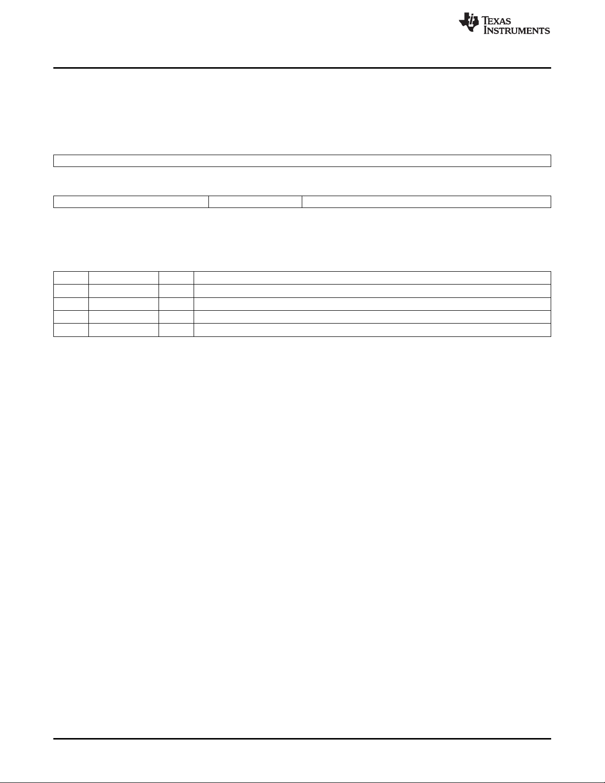
EMAC Port Registers
www.ti.com
5.4 Receive Identification and Version Register (RXIDVER)
The receive identification and version register (RXIDVER) is shown in Figure 46 and described in
Table 40.
Figure 46. Receive Identification and Version Register (RXIDVER)
31 16
RXIDENT
0x000C
15 11 10 8 7 0
RTLVER RXMAJORVER RXMINORVER
0x01 0x02 0x08
LEGEND: R = Read only; -n = value after reset
Table 40. Receive Identification and Version Register (RXIDVER) Field Descriptions
Bit Field Value Description
31-16 RXIDENT Receive identification value
15-11 RTLVER RTL version value
10-8 RXMAJORVER Receive major version value
7-0 RXMINORVER Receive minor version value
98
C6472/TCI6486 EMAC/MDIO SPRUEF8F–March 2006–Revised November 2010
Submit Documentation Feedback
Copyright © 2006–2010, Texas Instruments Incorporated
Page 99

www.ti.com
EMAC Port Registers
5.5 Receive Control Register (RXCONTROL)
The receive control register (RXCONTROL) is shown in Figure 47 and described in Table 41.
Figure 47. Receive Control Register (RXCONTROL)
31 16
Reserved
R-0
15 1 0
Reserved RXEN
R-0 R/W-0
LEGEND: R/W = Read/Write; R = Read only; -n = value after reset
Table 41. Receive Control Register (RXCONTROL) Field Descriptions
Bit Field Value Description
31-1 Reserved 0 Reserved
0 RXEN Receive DMA enable
0 Receive is disabled
1 Receive is enabled
SPRUEF8F–March 2006–Revised November 2010 C6472/TCI6486 EMAC/MDIO
Submit Documentation Feedback
Copyright © 2006–2010, Texas Instruments Incorporated
99
Page 100

EMAC Port Registers
www.ti.com
5.6 Receive Teardown Register (RXTEARDOWN)
The receive teardown register (RXTEARDOWN) is shown in Figure 48 and described in Table 42.
Figure 48. Receive Teardown Register (RXTEARDOWN)
31 16
RXTD
NRDY
15 3 2 0
Reserved RXTDNCH
R-0 R/W-0
LEGEND: R/W = Read/Write; R = Read only; -n = value after reset
Table 42. Receive Teardown Register (RXTEARDOWN) Field Descriptions
Bit Field Value Description
31 RXTDNRDY 0 Receive teardown ready. Read as zero, but is always assumed to be one (unused).
30-3 Reserved 0 Reserved
2-0 RXTDNCH Receive teardown channel. Receive channel teardown is commanded by writing the encoded value
of the receive channel to be torn down. The teardown register is read as zero.
0 Teardown receive channel 0
1h Teardown receive channel 1
2h Teardown receive channel 2
3h Teardown receive channel 3
4h Teardown receive channel 4
5h Teardown receive channel 5
6h Teardown receive channel 6
7h Teardown receive channel 7
Reserved
R-0
100
C6472/TCI6486 EMAC/MDIO SPRUEF8F–March 2006–Revised November 2010
Submit Documentation Feedback
Copyright © 2006–2010, Texas Instruments Incorporated
 Loading...