

Texas instruments TMS320F28062, TMS320F28068, TMS320F28067, TMS320F28069, TMS320F28064 ADVANCE INFORMATION
...Page 1

ADVANCEINFORMATION
TMS320F28069, TMS320F28068, TMS320F28067, TMS320F28066
TMS320F28065, TMS320F28064, TMS320F28063, TMS320F28062
www.ti.com
SPRS698A–NOVEMBER 2010–REVISED JANUARY 2011
Piccolo Microcontrollers
Check for
Samples: TMS320F28069, TMS320F28068, TMS320F28067, TMS320F28066, TMS320F28065, TMS320F28064, TMS320F28063,
1 TMS320F2806x ( Piccolo™) MCUs
1.1 Features
123
• High-Efficiency 32-Bit CPU (TMS320C28x™) • Peripheral Interrupt Expansion (PIE) Block That
– 80 MHz (12.5-ns Cycle Time)
– 16 x 16 and 32 x 32 MAC Operations
– 16 x 16 Dual MAC
– Harvard Bus Architecture
– Atomic Operations
– Fast Interrupt Response and Processing
– Unified Memory Programming Model
– Code-Efficient (in C/C++ and Assembly)
• Floating-Point Unit
– Native Single-Precision Floating-Point
Operations
• Programmable Control Law Accelerator (CLA)
– 32-Bit Floating-Point Math Accelerator
– Executes Code Independently of the Main
CPU
• Viterbi, Complex Math, CRC Unit (VCU)
– Extends C28x™ Instruction Set to Support
Complex Multiply, Viterbi Operations, and – Prevents Firmware Reverse Engineering
Cyclic Redundency Check (CRC)
• Embedded Memory
– Up to 256KB Flash (SCI) [UART] Modules
– Up to 100KB RAM – Two Serial Peripheral Interface (SPI)
– 2KB OTP ROM
• 6-Channel DMA
• Low Device and System Cost
– Single 3.3-V Supply
– No Power Sequencing Requirement
– Integrated Power-on Reset and Brown-out
Reset
– Low-Power Operating Modes
– No Analog Support Pin
• Clocking
– Two Internal Zero-pin Oscillators
– On-Chip Crystal Oscillator/External Clock
Input
– Dynamic PLL Ratio Changes Supported
– Watchdog Timer Module
– Missing Clock Detection Circuitry
1
Please be aware that an important notice concerning availability, standard warranty, and use in critical applications of Texas
Instruments semiconductor products and disclaimers thereto appears at the end of this data sheet.
2Piccolo, PowerPAD, C28x, TMS320C2000, C2000, Code Composer Studio, XDS510, XDS560, TMS320C28x, TMS320C54x, TMS320C55x
are trademarks of Texas Instruments.
3All other trademarks are the property of their respective owners.
ADVANCE INFORMATION concerns new products in the sampling
or preproduction phaseof development. Characteristic dataand other
specifications are subjectto change without notice.
TMS320F28062
Supports All Peripheral Interrupts
• Three 32-Bit CPU Timers
• Advanced Control Peripherals
• Up to 8 Enhanced Pulse Width Modulator
(ePWM) Modules
– 16 PWM Channels Total (8 HRPWM-Capable)
– Independent 16-Bit Timer in Each Module
• 3 Input Capture (eCAP) Modules
• 4 High-Resolution Input Capture (HRCAP)
Modules
• 2 Quadrature Encoder (eQEP) Modules
• 12-Bit ADC, Dual Sample-and-Hold
– Up to 3 MSPS
– Up to 16 Channels
• On-Chip Temperature Sensor
• 128-Bit Security Key/Lock
– Protects Secure Memory Blocks
• Serial Port Peripherals
– Up to Two Serial Communications Interface
Modules
– One Inter-Integrated-Circuit (I2C) Bus
– One Multi-Channel Buffered Serial Port
(McBSP) Bus
– One Enhanced Controller Area Network
(eCAN)
• Up to 54 Individually Programmable,
Multiplexed GPIO Pins With Input Filtering
• Advanced Emulation Features
– Analysis and Breakpoint Functions
– Real-Time Debug via Hardware
• 2806x Packages
– 80-Pin PFP and 100-Pin PZP PowerPAD™
Low-Profile Quad Flatpacks (LQFPs)
– 80-Pin PN and 100-Pin PZ LQFPs
Copyright © 2010–2011, Texas Instruments Incorporated
Page 2

ADVANCEINFORMATION
TMS320F28069, TMS320F28068, TMS320F28067, TMS320F28066
TMS320F28065, TMS320F28064, TMS320F28063, TMS320F28062
SPRS698A–NOVEMBER 2010–REVISED JANUARY 2011
1.2 Description
The F2806x Piccolo™ family of microcontrollers provides the power of the C28x™ core and Control Law
Accelerator (CLA) coupled with highly integrated control peripherals in low pin-count devices. This family
is code-compatible with previous C28x-based code, as well as providing a high level of analog integration.
An internal voltage regulator allows for single-rail operation. Enhancements have been made to the
HRPWM module to allow for dual-edge control (frequency modulation). Analog comparators with internal
10-bit references have been added and can be routed directly to control the PWM outputs. The ADC
converts from 0 to 3.3-V fixed full scale range and supports ratio-metric V
ADC interface has been optimized for low overhead/latency.
REFHI/VREFLO
www.ti.com
references. The
2 TMS320F2806x ( Piccolo™) MCUs Copyright © 2010–2011, Texas Instruments Incorporated
Submit Documentation Feedback
Product Folder Link(s): TMS320F28069 TMS320F28068 TMS320F28067 TMS320F28066 TMS320F28065
TMS320F28064 TMS320F28063 TMS320F28062
Page 3
ADVANCEINFORMATION
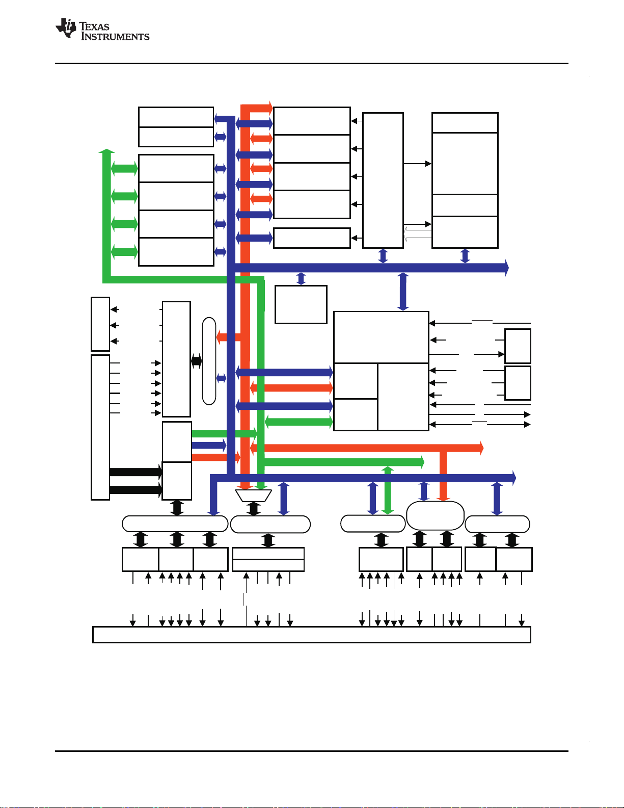
CLA Bus
GPIO Mux
DMA Bus
DMA Bus
16-bit Peripheral Bus
32-bit Peripheral Bus
(CLA accessible)
32-bit Peripheral
Bus
32-bit Peripheral
Bus
32-bit
Peripheral Bus
(CLA accessible)
SCITXDx
SCIRXDx
SPISIMOx
SPISOMIx
SPICLKx
SPISTEx
SDAx
SCLx
TZx
EPWMxA
EPWMxB
ESYNCI
ESYNCO
MFSRA
MDRA
MCLKRA
MFSXA
MDXA
MCLKXA
ECAPx
EQEPxA
EQEPxB
EQEPxI
EQEPxS
HRCAPx
CANRXx
CANTXx
SCI-A/B
(4L FIFO)
SPI-A/B
(4L FIFO)
I2C-A
(4L FIFO)
ePWM1 to ePWM8
HRPWM (8ch)
McBSP-A
eCAP-
1/2/3
eQEP-
1/2
HRCAP-
1/2/3/4
eCAN-A
(32-mbox)
Memory Bus
A7:0
B7:0
Memory Bus
Memory Bus
DMA Bus
CLA Bus
DMA Bus
GPIO Mux
AIO Mux
32-bit Peripheral Bus
GPIO
Mux
GPIO
Mux
ADC
0-wait
Result
Regs
ADC
COMP
+
DAC
COMP1OUT
COMP2OUT
COMP3OUT
COMP1A
COMP2A
COMP3A
COMP1B
COMP2B
COMP3B
Boot-ROM
(32Kx16)
(0-wait,
Non-Secure)
CLA +
Message
RAMs
DMA
6-ch
C28x 32-bit CPU
FPU
VCU
OSC1, OSC2,
Ext, PLLs,
LPM, WD,
CPU Timers
0/1/2. PIE
TRST
TCK, TDI, TMS
TDO
XCLKIN
LPM Wakeup
3 Ext. Interrupts
X1
X2
XRS
PSWD
M0 SARAM (1Kx16)
(0-wait, Non-Secure)
M1 SARAM (1Kx16)
(0-wait, Non-Secure)
L5 DPSARAM (8Kx16)
(0-wait, Non-Secure)
DMA RAM0
L6 DPSARAM (8Kx16)
(0-wait, Non-Secure)
DMA RAM1
L7 DPSARAM (8Kx16)
(0-wait, Non-Secure)
DMA RAM2
L8 DPSARAM (8Kx16)
(0-wait, Non-Secure)
DMA RAM3
L0 DPSARAM (2Kx16)
(0-wait, Secure)
CLA Data RAM2
L1 DPSARAM (1Kx16)
(0-wait, Secure)
CLA Data RAM0
L2 DPSARAM (1Kx16)
(0-wait, Secure)
CLA Data RAM1
L3 DPSARAM (4Kx16)
(0-wait, Secure)
CLA Program RAM
L4 SARAM (8Kx16)
(0-wait, Secure)
Code
Security
Module
(CSM)
OTP 1Kx16
Secure
FLASH
64K/128Kx16
8 equal sectors
Secure
PUMP
OTP/Flash
Wrapper
www.ti.com
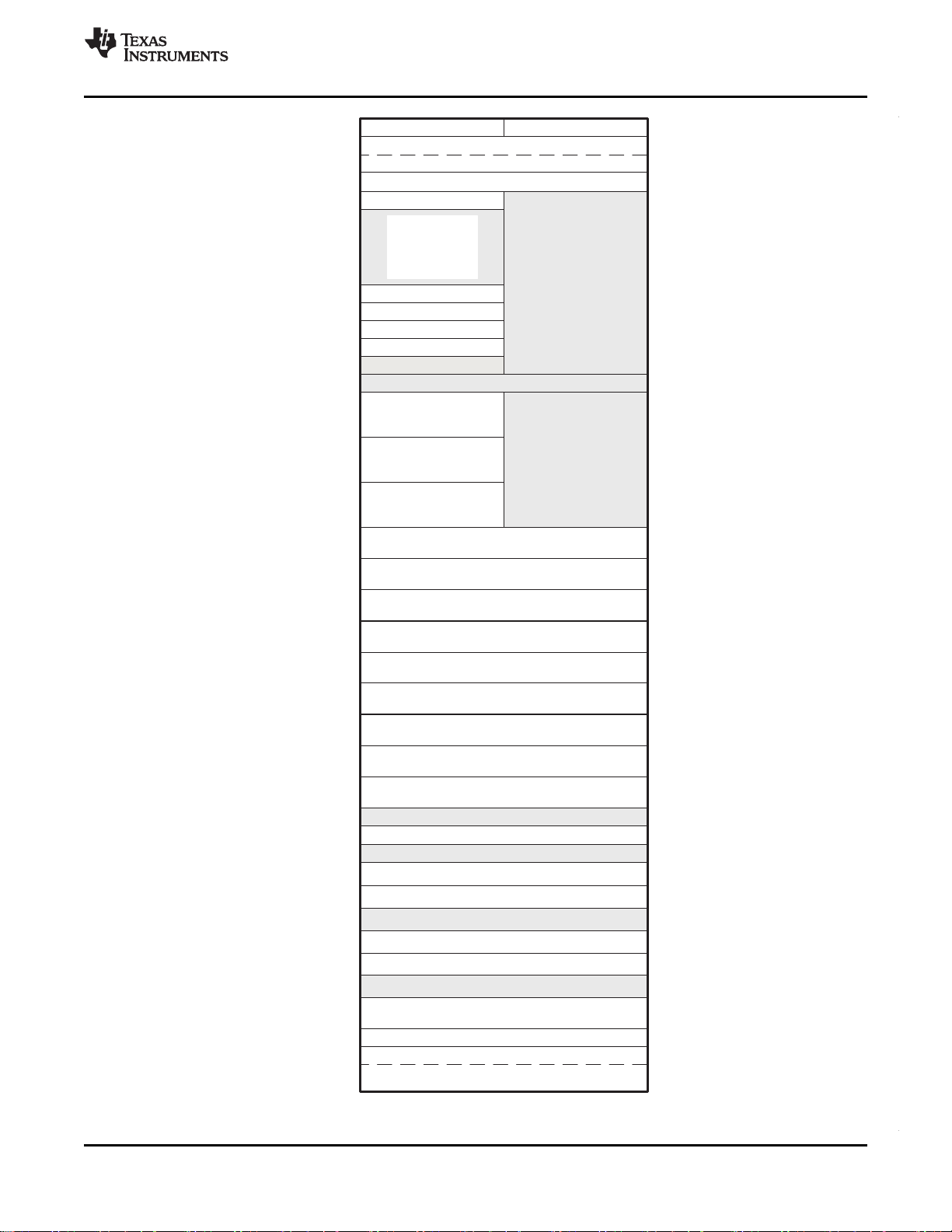
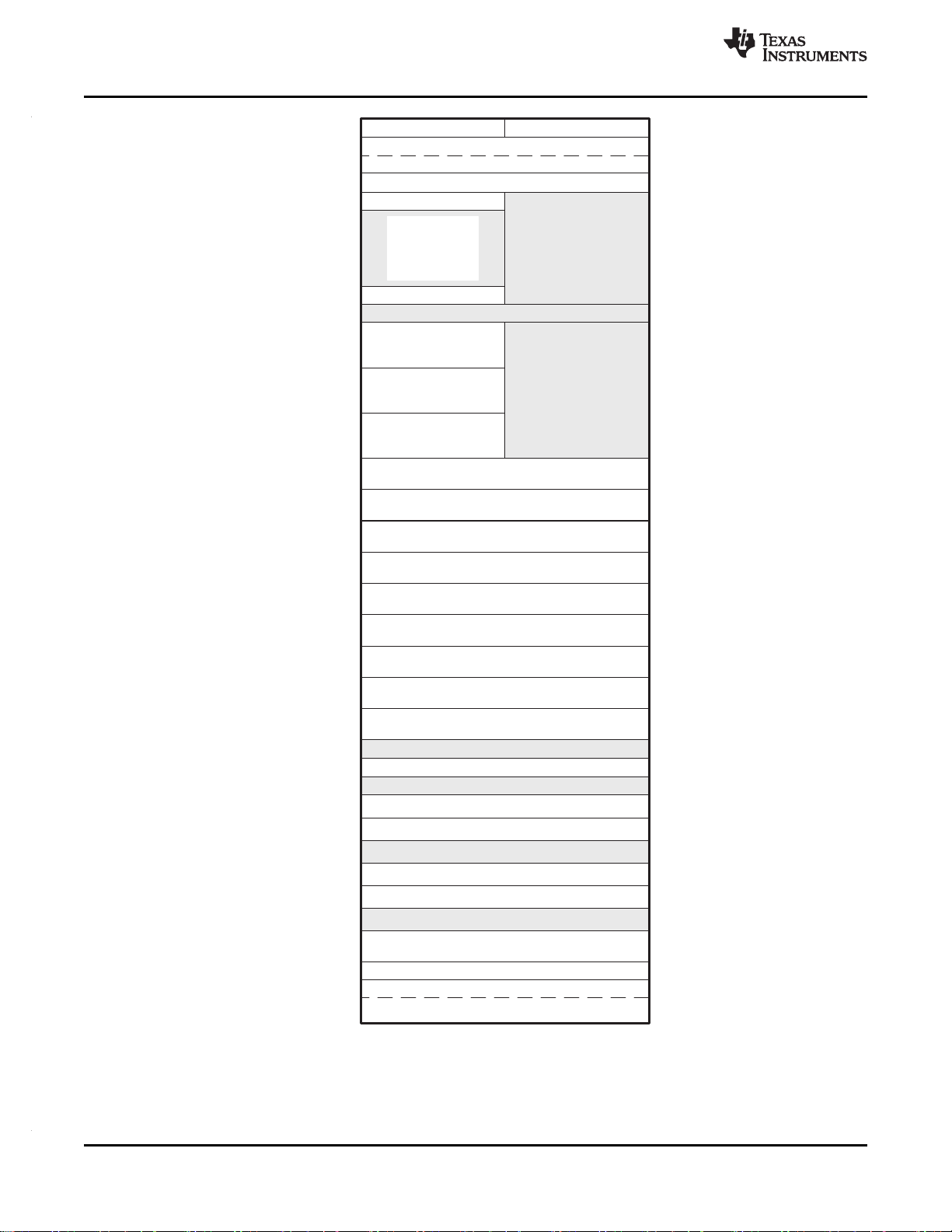
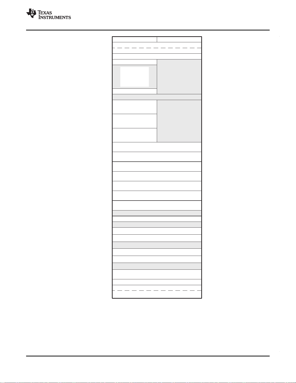
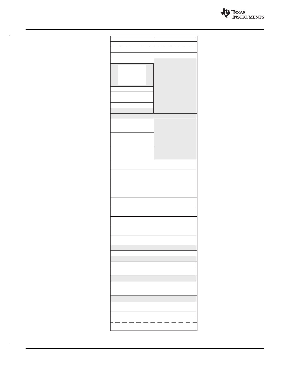
1.3 Functional Block Diagram
TMS320F28069, TMS320F28068, TMS320F28067, TMS320F28066
TMS320F28065, TMS320F28064, TMS320F28063, TMS320F28062
SPRS698A–NOVEMBER 2010–REVISED JANUARY 2011
A. Not all peripheral pins are available at the same time due to multiplexing.
Figure 1-1. Functional Block Diagram
Copyright © 2010–2011, Texas Instruments Incorporated TMS320F2806x ( Piccolo™) MCUs 3
Product Folder Link(s): TMS320F28069 TMS320F28068 TMS320F28067 TMS320F28066 TMS320F28065
Submit Documentation Feedback
TMS320F28064 TMS320F28063 TMS320F28062
Page 4
ADVANCEINFORMATION
10-bit
DAC
Analog
Comparators
CMP1-Out
CMP2-Out
CMP3-Out
Trip Zone
Temp
Sensor
ADC
(DMA-
accessible)
12-bit
3-MSPS
Dual-S/H
SOC-
based
V
REF
CLA Core
80-MHz Floating-Point
(Accelerator)
(DMA-accessible)
10-bit
DAC
10-bit
DAC
A0
A2
A3
A4
A5
A6
A7
B0
B1
B2
B3
B4
B5
B6
B7
A1
6
eQEP x 2
HRCAP x 4
eCAP x 3
System
Vreg
Int-Osc-1
POR/BOR
Int-Osc-2
On-chip Osc
WD
PLL
CLKSEL
Timers 32-bit
Timer-0
Timer-1
Timer-2
GPIO
Control
COMMS
X1
X2
V
REFLO
V
REFHI
C28x
Core
(80-MHz)
FPU
VCU
Flash Memory
RAM
RAM
(Dual-Access)
eQEP
8
HRCAP
4
eCAP
3
4
8
2
2
6
PWM-1A
PWM-1B
PWM-2A
PWM-2B
PWM-3A
PWM-3B
PWM-4A
PWM-4B
PWM-5A
PWM-5B
PWM-6A
PWM-6B
PWM-7A
PWM-7B
PWM-8A
PWM-8B
TZ1
TZ2
TZ3
CMP1-out
CMP2-out
CMP3-out
PWM1
(DMA-accessible)
PWM5
(DMA-accessible)
PWM8
(DMA-accessible)
PWM7
(DMA-accessible)
PWM6
(DMA-accessible)
PWM4
(DMA-accessible)
PWM3
(DMA-accessible)
PWM2
(DMA-accessible)
UART x 2
SPI x 2
I2C
CAN
McBSP
(DMA-accessible)
TMS320F28069, TMS320F28068, TMS320F28067, TMS320F28066
TMS320F28065, TMS320F28064, TMS320F28063, TMS320F28062
SPRS698A–NOVEMBER 2010–REVISED JANUARY 2011
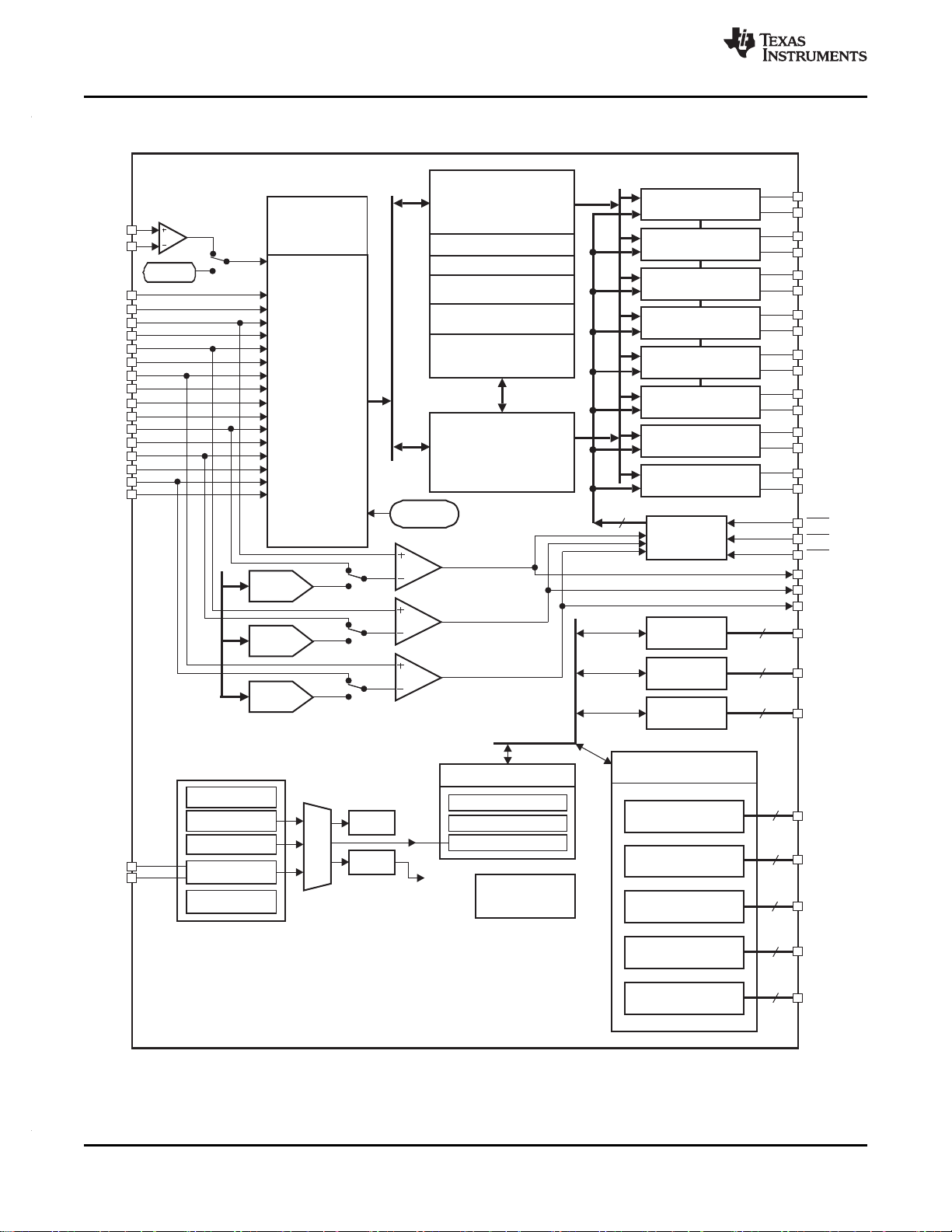
1.4 System Device Diagram
www.ti.com
4 TMS320F2806x ( Piccolo™) MCUs Copyright © 2010–2011, Texas Instruments Incorporated
Product Folder Link(s): TMS320F28069 TMS320F28068 TMS320F28067 TMS320F28066 TMS320F28065
TMS320F28064 TMS320F28063 TMS320F28062
Figure 1-2. Peripheral Blocks
Submit Documentation Feedback
Page 5

ADVANCEINFORMATION
www.ti.com
TMS320F28069, TMS320F28068, TMS320F28067, TMS320F28066
TMS320F28065, TMS320F28064, TMS320F28063, TMS320F28062
SPRS698A–NOVEMBER 2010–REVISED JANUARY 2011
1 TMS320F2806x ( Piccolo™) MCUs .................. 1
1.1 Features .............................................. 1
1.2 Description ........................................... 2
1.3 Functional Block Diagram ............................ 3
1.4 System Device Diagram ............................. 4 6.6 Current Consumption ............................... 67
2 Revision History ......................................... 6
3 Device Overview ........................................ 7
3.1 Device Characteristics ............................... 7
3.2 Memory Maps ...................................... 10
3.3 Pin Assignments .................................... 20
3.4 Signal Descriptions ................................. 22
3.5 Brief Descriptions ................................... 31
3.6 Register Map ....................................... 40
3.7 Device Emulation Registers ........................ 42
3.8 VREG/BOR/POR ................................... 43
3.9 System Control ..................................... 45
3.10 Low-power Modes Block ........................... 53
4 Device and Documentation Support ............... 54
4.1 Getting Started ..................................... 54
4.2 Development Support .............................. 54
4.3 Device and Development Support Tool
Nomenclature ....................................... 54
4.4 Documentation Support ............................ 56
4.5 Community Resources ............................. 57
5 Device Operating Conditions ....................... 58
5.1 Absolute Maximum Ratings ........................ 58
5.2 Recommended Operating Conditions .............. 58
5.3 Electrical Characteristics ........................... 59
6 Peripheral and Electrical Specifications .......... 60
6.1 Parameter Information .............................. 60
6.2 Test Load Circuit ................................... 60
6.3 Device Clock Table ................................. 61
6.4 Clock Requirements and Characteristics ........... 63
6.5 Power Sequencing ................................. 64
6.7 Emulator Connection Without Signal Buffering for
the MCU ............................................ 69
6.8 Interrupts ............................................ 70
6.9 Control Law Accelerator (CLA) Overview .......... 75
6.10 Analog Block ........................................ 78
6.11 Detailed Descriptions ............................... 92
6.12 Serial Peripheral Interface (SPI) Module ........... 93
6.13 Serial Communications Interface (SCI) Module
..................................................... 102
6.14 Multichannel Buffered Serial Port (McBSP) Module
..................................................... 105
6.15 Enhanced Controller Area Network (eCAN) Module
..................................................... 115
6.16 Inter-Integrated Circuit (I2C) ...................... 119
6.17 Enhanced Pulse Width Modulator (ePWM) Modules
(ePWM1/2/3/4/5/6/7/8) ............................ 122
6.18 High-Resolution PWM (HRPWM) ................. 129
6.19 Enhanced Capture Module (eCAP1) .............. 130
6.20 High-Resolution Capture (HRCAP) Module ....... 132
6.21 Enhanced Quadrature Encoder Modules (eQEP1/2)
..................................................... 133
6.22 JTAG Port ......................................... 136
6.23 General-Purpose Input/Output (GPIO) MUX ...... 137
6.24 Flash Timing ....................................... 149
7 Mechanical Packaging and Orderable
Information ............................................ 151
7.1 Thermal Data ...................................... 151
7.2 Packaging Information ............................ 152
Copyright © 2010–2011, Texas Instruments Incorporated Contents 5
Submit Documentation Feedback
Product Folder Link(s): TMS320F28069 TMS320F28068 TMS320F28067 TMS320F28066 TMS320F28065
TMS320F28064 TMS320F28063 TMS320F28062
Page 6

ADVANCEINFORMATION
TMS320F28069, TMS320F28068, TMS320F28067, TMS320F28066
TMS320F28065, TMS320F28064, TMS320F28063, TMS320F28062
SPRS698A–NOVEMBER 2010–REVISED JANUARY 2011
2 Revision History
This data sheet revision history highlights the technical changes made to the SPRS698 device-specific
data sheet to make it an SPRS698A revision.
Scope: Added 80-pin PN package and 100-pin PZ package.
Added "T" temperature range (–40°C to 105°C).
Added new sections.
Information/data on the TMS320F2806x devices is now Advance Information.
ADVANCE INFORMATION concerns new products in the sampling or preproduction phase of
development. Characteristic data and other specifications are subject to change without notice.
LOCATION ADDITIONS, DELETIONS, AND MODIFICATIONS
Global
Section 1
TMS320F2806x
(Piccolo™) MCUs
Section 3
Device Overview
Section 4
Device and
Documentation Support
Section 7
Mechanical Packaging
and Orderable
Information
• Added 80-pin PN package
• Added 100-pin PZ package
• Added "T" temperature range (–40°C to 105°C)
• Added Section 1.2, Description
• Figure 1-1, Functional Block Diagram:
– Removed "32-bit Peripheral Bus"
• Table 3-1, Hardware Features:
– 6-Channel DMA: Added "0" to TYPE column
– High-resolution capture modules (HRCAP): Added "0" to TYPE column
– Multi-Channel Buffered Serial Port (McBSP): Added "1" to TYPE column
– Updated "Temperature options"
• Added Section 3.2, Memory Maps
• Figure 3-8, 80-Pin PN/PFP LQFP (Top View):
– Removed SCI-B signals and eQEP2 signals
• Table 3-6, Terminal Functions:
– Added "SCI-B is only available in the PZ and PZP packages" note to DESCRIPTION of PN/PFP pins# 39,
59, 76, 70, 41, 52, 78, 1
– Added "eQEP2 is only available in the PZ and PZP packages" note to DESCRIPTION of PN/PFP
pins# 77, 31, 62, 61, 33, 32
• Added Section 3.5, Brief Descriptions
• Added Section 3.6, Register Map
• Added Section 3.7, Device Emulation Registers
• Added Section 3.8, VREG/BOR/POR
• Added Section 3.9, System Control
• Added Section 3.10, Low-power Modes Block
• Added Section 4.1, Getting Started
• Section 4.3, Device and Development Support Tool Nomenclature:
– Updated PACKAGE TYPE in Figure 4-1, Device Nomenclature
• Added Section 4.4, Documentation Support
Added Section 6, Peripheral and Electrical Specifications
• Added Section 7.1, Thermal Data
www.ti.com
6 Revision History Copyright © 2010–2011, Texas Instruments Incorporated
Submit Documentation Feedback
Product Folder Link(s): TMS320F28069 TMS320F28068 TMS320F28067 TMS320F28066 TMS320F28065
TMS320F28064 TMS320F28063 TMS320F28062
Page 7

ADVANCEINFORMATION
www.ti.com
3 Device Overview
3.1 Device Characteristics
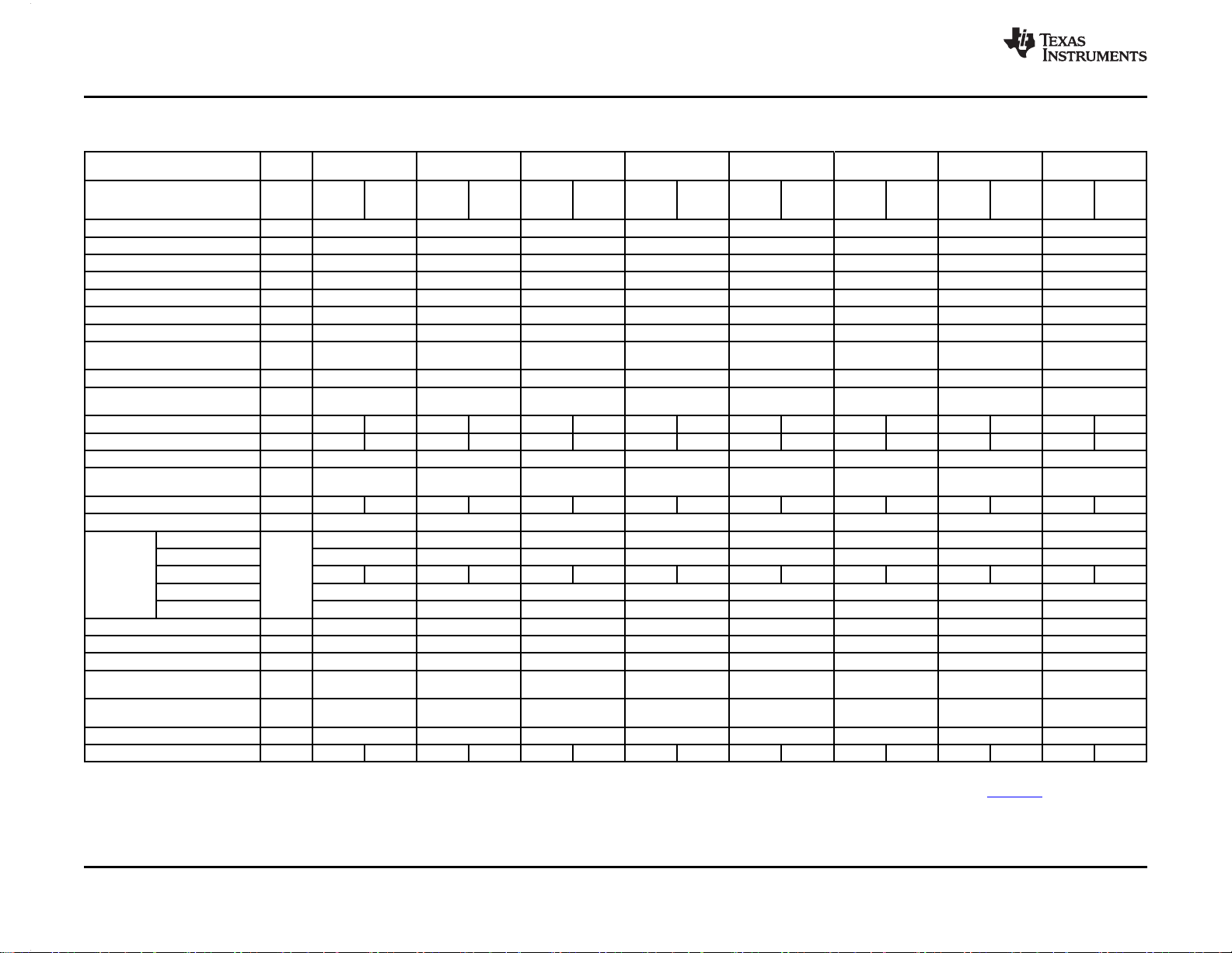
Table 3-1 lists the features of the TMS320F2806x devices.
TMS320F28069, TMS320F28068, TMS320F28067, TMS320F28066
TMS320F28065, TMS320F28064, TMS320F28063, TMS320F28062
SPRS698A–NOVEMBER 2010–REVISED JANUARY 2011
Copyright © 2010–2011, Texas Instruments Incorporated Device Overview 7
Submit Documentation Feedback
Product Folder Link(s): TMS320F28069 TMS320F28068 TMS320F28067 TMS320F28066 TMS320F28065
TMS320F28064 TMS320F28063 TMS320F28062
Page 8
ADVANCEINFORMATION
TMS320F28069, TMS320F28068, TMS320F28067, TMS320F28066
TMS320F28065, TMS320F28064, TMS320F28063, TMS320F28062
SPRS698A–NOVEMBER 2010–REVISED JANUARY 2011
Table 3-1. Hardware Features
www.ti.com
FEATURE TYPE
Package Type PZ/PZP PN/PFP PZ/PZP PN/PFP PZ/PZP PN/PFP PZ/PZP PN/PFP PZ/PZP PN/PFP PZ/PZP PN/PFP PZ/PZP PN/PFP PZ/PZP PN/PFP
Instruction cycle – 12.5 ns 12.5 ns 12.5 ns 12.5 ns 12.5 ns 12.5 ns 12.5 ns 12.5 ns
Floating-Point Unit (FPU) Yes Yes Yes Yes Yes Yes Yes Yes
Viterbi, Complex Math,CRC Unit (VCU) Yes Yes No No Yes Yes No No
Control Law Accelerator(CLA) 0 Yes No No No Yes No No No
6-Channel DMA 0 Yes Yes Yes Yes Yes Yes Yes Yes
On-chip Flash (16-bitword) – 128K 128K 128K 128K 64K 64K 64K 64K
On-chip SARAM (16-bitword) – 50K 50K 50K 34K 50K 50K 34K 26K
Code security foron-chip
flash/SARAM/OTP blocks
Boot ROM (32Kx 16) – Yes Yes Yes Yes Yes Yes Yes Yes
One-time programmable (OTP)ROM
(16-bit word)
ePWM outputs 1 19 15 19 15 19 15 19 15 19 15 19 15 19 15 19 15
High-resolution ePWM Channels 1 8 6 8 6 8 6 8 6 8 6 8 6 8 6 8 6
eCAP inputs 0 3 3 3 3 3 3 3 3
High-resolution capture modules
(HRCAP)
eQEP modules 0 2 1 2 1 2 1 2 1 2 1 2 1 2 1 2 1
Watchdog timer – Yes Yes Yes Yes Yes Yes Yes Yes
MSPS 3 3 3 3 3 3 3 3
Conversion Time 325 ns 325 ns 325 ns 325 ns 325 ns 325 ns 325 ns 325 ns
12-Bit ADC Channels 3 16 12 16 12 16 12 16 12 16 12 16 12 16 12 16 12
Temperature Sensor Yes Yes Yes Yes Yes Yes Yes Yes
Dual Sample-and-Hold Yes Yes Yes Yes Yes Yes Yes Yes
32-Bit CPU timers – 3 3 3 3 3 3 3 3
Comparators with IntegratedDACs 0 3 3 3 3 3 3 3 3
Inter-integrated circuit (I2C) 0 1 1 1 1 1 1 1 1
Multi-Channel Buffered SerialPort
(McBSP)
Enhanced Controller AreaNetwork
(eCAN)
Serial Peripheral Interface(SPI) 1 2 2 2 2 2 2 2 2
Serial Communications Interface(SCI) 0 2 1 2 1 2 1 2 1 2 1 2 1 2 1 2 1
(1)
– Yes Yes Yes Yes Yes Yes Yes Yes
– 1K 1K 1K 1K 1K 1K 1K 1K
0 4 4 4 4 4 4 4 4
1 1 1 1 1 1 1 1 1
0 1 1 1 1 1 1 1 1
28069 28068 28067 28066 28065 28064 28063 28062
(80 MHz) (80 MHz) (80 MHz) (80 MHz) (80 MHz) (80 MHz) (80 MHz) (80 MHz)
100-Pin 80-Pin 100-Pin 80-Pin 100-Pin 80-Pin 100-Pin 80-Pin 100-Pin 80-Pin 100-Pin 80-Pin 100-Pin 80-Pin 100-Pin 80-Pin
LQFP LQFP LQFP LQFP LQFP LQFP LQFP LQFP LQFP LQFP LQFP LQFP LQFP LQFP LQFP LQFP
(1) A type change represents a major functional feature difference in a peripheral module. Within a peripheral type, there may be minor differences between devices that do not affect the
basic functionality of the module. These device-specific differences are listed in the TMS320x28xx, 28xxx DSP Peripheral Reference Guide (literature number SPRU566) and in the
peripheral reference guides.
8 Device Overview Copyright © 2010–2011, Texas Instruments Incorporated
Submit Documentation Feedback
Product Folder Link(s): TMS320F28069 TMS320F28068 TMS320F28067 TMS320F28066 TMS320F28065
TMS320F28064 TMS320F28063 TMS320F28062
Page 9
ADVANCEINFORMATION
TMS320F28069, TMS320F28068, TMS320F28067, TMS320F28066
TMS320F28065, TMS320F28064, TMS320F28063, TMS320F28062
www.ti.com
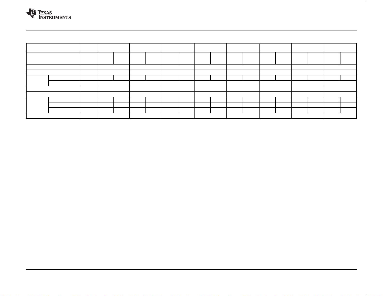
Table 3-1. Hardware Features (continued)
FEATURE TYPE
Package Type PZ/PZP PN/PFP PZ/PZP PN/PFP PZ/PZP PN/PFP PZ/PZP PN/PFP PZ/PZP PN/PFP PZ/PZP PN/PFP PZ/PZP PN/PFP PZ/PZP PN/PFP
2-pin Oscillator 1 1 1 1 1 1 1 1
0-pin Oscillator 2 2 2 2 2 2 2 2
I/O pins
(shared)
External interrupts – 3 3 3 3 3 3 3 3
Supply voltage (nominal) – 3.3 V 3.3 V 3.3 V 3.3 V 3.3 V 3.3 V 3.3 V 3.3 V
Temperature
options
Product status
GPIO – 54 40 54 40 54 40 54 40 54 40 54 40 54 40 54 40
AIO – 6 6 6 6 6 6 6 6
T: –40°C to 105°C – PZ PN PZ PN PZ PN PZ PN PZ PN PZ PN PZ PN PZ PN
S: –40°C to 125°C – PZP PFP PZP PFP PZP PFP PZP PFP PZP PFP PZP PFP PZP PFP PZP PFP
Q: –40°C to 125°C
(2)
(1)
(1)
– PZP PFP PZP PFP PZP PFP PZP PFP PZP PFP PZP PFP PZP PFP PZP PFP
– TMX TMX TMX TMX TMX TMX TMX TMX
(1) "Q" refers to Q100 qualification for automotive applications.
(2) See Section 4.3, Device and Development Support Tool Nomenclature, for descriptions of device stages. The "TMX" product status denotes an experimental device that is not necessarily
representative of the final device's electrical specifications.
28069 28068 28067 28066 28065 28064 28063 28062
(80 MHz) (80 MHz) (80 MHz) (80 MHz) (80 MHz) (80 MHz) (80 MHz) (80 MHz)
100-Pin 80-Pin 100-Pin 80-Pin 100-Pin 80-Pin 100-Pin 80-Pin 100-Pin 80-Pin 100-Pin 80-Pin 100-Pin 80-Pin 100-Pin 80-Pin
LQFP LQFP LQFP LQFP LQFP LQFP LQFP LQFP LQFP LQFP LQFP LQFP LQFP LQFP LQFP LQFP
SPRS698A–NOVEMBER 2010–REVISED JANUARY 2011
Copyright © 2010–2011, Texas Instruments Incorporated Device Overview 9
Submit Documentation Feedback
Product Folder Link(s): TMS320F28069 TMS320F28068 TMS320F28067 TMS320F28066 TMS320F28065
TMS320F28064 TMS320F28063 TMS320F28062
Page 10

ADVANCEINFORMATION
TMS320F28069, TMS320F28068, TMS320F28067, TMS320F28066
TMS320F28065, TMS320F28064, TMS320F28063, TMS320F28062
SPRS698A–NOVEMBER 2010–REVISED JANUARY 2011
3.2 Memory Maps
In Figure 3-1 through Figure 3-7, the following apply:
• Memory blocks are not to scale.
• Peripheral Frame 0, Peripheral Frame 1, Peripheral Frame 2, and Peripheral Frame 3 memory maps
are restricted to data memory only. A user program cannot access these memory maps in program
space.
• Protected means the order of Write-followed-by-Read operations is preserved rather than the pipeline
order.
• Certain memory ranges are EALLOW protected against spurious writes after configuration.
• Locations 0x3D 7C80–0x3D 7CC0 contain the internal oscillator and ADC calibration routines. These
locations are not programmable by the user.
www.ti.com
10 Device Overview Copyright © 2010–2011, Texas Instruments Incorporated
Submit Documentation Feedback
Product Folder Link(s): TMS320F28069 TMS320F28068 TMS320F28067 TMS320F28066 TMS320F28065
TMS320F28064 TMS320F28063 TMS320F28062
Page 11
ADVANCEINFORMATION
M0 Vector RAM (Enabled if VMAP = 0)
M0 SARAM (1K x 16, 0-Wait)
0x00 0000
0x00 0040
M1 SARAM (1K x 16, 0-Wait)
0x00 0400
Data Space Prog Space
Reserved
0x00 2000
Reserved
Peripheral Frame 0
0x00 0800
0x00 1580
0x00 0D00
PIE Vector - RAM
(256 x 16)
(Enabled if
VMAP = 1,
ENPIE = 1)
0x00 1400
0x00 0E00
0x00 1500
0x00 1480
CPU-to-CLA Message RAM
CLA-to-CPU Message RAM
CLA Registers
Peripheral Frame 0
Peripheral Frame 3
(4K x 16, Protected)
DMA-Accessible
0x00 5000
Peripheral Frame 2
(4K x 16, Protected)
0x00 7000
0x00 8000
L0 DPSARAM (2K x 16)
(0-Wait, Secure Zone + ECSL, CLA Data RAM2)
0x00 8800
L1 DPSARAM (1K x 16)
(0-Wait, Secure Zone + ECSL, CLA Data RAM 0)
0x00 8C00
L2 DPSARAM (1K x 16)
(0-Wait, Secure Zone + ECSL, CLA Data RAM 1)
0x00 9000
L3 DPSARAM (4K x 16)
(0-Wait, Secure Zone + ECSL, CLA Program RAM)
0x00 A000
L4 SARAM (8K x 16)
(0-Wait, Secure Zone + ECSL, Dual Mapped)
0x00 C000
L5 DPSARAM (8K x 16)
(0-Wait, DMA RAM 0)
L8 DPSARAM (8K x 16)
(0-Wait, DMA RAM 3)
L7 DPSARAM (8K x 16)
(0-Wait, DMA RAM 2)
L6 DPSARAM (8K x 16)
(0-Wait, DMA RAM 1)
0x00 E000
0x01 0000
0x01 2000
Peripheral Frame 1
(4K x 16, Protected)
0x00 6000
Reserved
0x3D 7800
User OTP (1K x 16, Secure Zone + ECSL)
0x3D 7C80
Calibration Data
0x01 4000
Reserved
0x3D 7BFA
Reserved
FLASH
(128K x 16, 8 Sectors, Secure Zone + ECSL)
128-Bit Password
0x3D 8000
0x3F 7FF8
Boot ROM (32K x 16, 0-Wait)
Vector (32 Vectors, Enabled if VMAP = 1)
0x3F 8000
0x3F FFC0
0x3D 7CC0
Get_mode function
0x3D 7CD0
Reserved
0x3D 7E80
PARTID
Calibration Data
Reserved
0x3D 7EB0
Reserved
TMS320F28069, TMS320F28068, TMS320F28067, TMS320F28066
TMS320F28065, TMS320F28064, TMS320F28063, TMS320F28062
www.ti.com
Copyright © 2010–2011, Texas Instruments Incorporated Device Overview 11
Product Folder Link(s): TMS320F28069 TMS320F28068 TMS320F28067 TMS320F28066 TMS320F28065
Figure 3-1. 28069 Memory Map
Submit Documentation Feedback
TMS320F28064 TMS320F28063 TMS320F28062
SPRS698A–NOVEMBER 2010–REVISED JANUARY 2011
Page 12
ADVANCEINFORMATION
M0 Vector RAM (Enabled if VMAP = 0)
M0 SARAM (1K x 16, 0-Wait)
0x00 0000
0x00 0040
M1 SARAM (1K x 16, 0-Wait)
0x00 0400
Data Space Prog Space
Reserved
Peripheral Frame 0
0x00 0800
0x00 0D00
PIE Vector - RAM
(256 x 16)
(Enabled if
VMAP = 1,
ENPIE = 1)
0x00 0E00
Peripheral Frame 0
0x00 1400
Reserved
Peripheral Frame 2
(4K x 16, Protected)
0x00 7000
0x00 8000
L0 DPSARAM (2K x 16)
(0-Wait, Secure Zone + ECSL)
0x00 8800
L1 DPSARAM (1K x 16)
(0-Wait, Secure Zone + ECSL)
0x00 8C00
L2 DPSARAM (1K x 16)
(0-Wait, Secure Zone + ECSL)
0x00 9000
L3 DPSARAM (4K x 16)
(0-Wait, Secure Zone + ECSL)
0x00 A000
L4 SARAM (8K x 16)
(0-Wait, Secure Zone + ECSL, Dual Mapped)
0x00 C000
L5 DPSARAM (8K x 16)
(0-Wait, DMA RAM 0)
L8 DPSARAM (8K x 16)
(0-Wait, DMA RAM 3)
L7 DPSARAM (8K x 16)
(0-Wait, DMA RAM 2)
L6 DPSARAM (8K x 16)
(0-Wait, DMA RAM 1)
0x00 E000
0x01 0000
0x01 2000
Peripheral Frame 1
(4K x 16, Protected)
0x00 6000
Reserved
0x01 4000
Reserved
Peripheral Frame 3
(4K x 16, Protected)
DMA-Accessible
0x00 5000
0x3D 7800
User OTP (1K x 16, Secure Zone + ECSL)
0x3D 7C80
Calibration Data
0x3D 7BFA
Reserved
FLASH
(128K x 16, 8 Sectors, Secure Zone + ECSL)
128-Bit Password
0x3D 8000
0x3F 7FF8
Boot ROM (32K x 16, 0-Wait)
Vector (32 Vectors, Enabled if VMAP = 1)
0x3F 8000
0x3F FFC0
0x3D 7CC0
Get_mode function
0x3D 7CD0
Reserved
0x3D 7E80
PARTID
Calibration Data
Reserved
0x3D 7EB0
TMS320F28069, TMS320F28068, TMS320F28067, TMS320F28066
TMS320F28065, TMS320F28064, TMS320F28063, TMS320F28062
SPRS698A–NOVEMBER 2010–REVISED JANUARY 2011
12 Device Overview Copyright © 2010–2011, Texas Instruments Incorporated
Product Folder Link(s): TMS320F28069 TMS320F28068 TMS320F28067 TMS320F28066 TMS320F28065
Figure 3-2. 28068/28067 Memory Map
Submit Documentation Feedback
TMS320F28064 TMS320F28063 TMS320F28062
www.ti.com
Page 13
ADVANCEINFORMATION
M0 Vector RAM (Enabled if VMAP = 0)
M0 SARAM (1K x 16, 0-Wait)
0x00 0000
0x00 0040
M1 SARAM (1K x 16, 0-Wait)
0x00 0400
Data Space Prog Space
Reserved
Peripheral Frame 0
0x00 0800
0x00 0D00
PIE Vector - RAM
(256 x 16)
(Enabled if
VMAP = 1,
ENPIE = 1)
0x00 0E00
Peripheral Frame 0
0x00 1400
Reserved
Peripheral Frame 1
(4K x 16, Protected)
Peripheral Frame 2
(4K x 16, Protected)
0x00 7000
0x00 6000
0x00 8000
L0 DPSARAM (2K x 16)
(0-Wait, Secure Zone + ECSL)
0x00 8800
L1 DPSARAM (1K x 16)
(0-Wait, Secure Zone + ECSL)
0x00 8C00
L2 DPSARAM (1K x 16)
(0-Wait, Secure Zone + ECSL)
0x00 9000
L3 DPSARAM (4K x 16)
(0-Wait, Secure Zone + ECSL)
0x00 A000
L4 SARAM (8K x 16)
(0-Wait, Secure Zone + ECSL, Dual Mapped)
0x00 C000
L5 DPSARAM (8K x 16)
(0-Wait, DMA RAM 0)
L6 DPSARAM (8K x 16)
(0-Wait, DMA RAM 1)
0x00 E000
Reserved
0x01 0000
Reserved
0x00 5000
Peripheral Frame 3
(4K x 16, Protected)
DMA-Accessible
0x3D 7800
User OTP (1K x 16, Secure Zone + ECSL)
0x3D 7C80
Calibration Data
0x3D 7BFA
Reserved
FLASH
(128K x 16, 8 Sectors, Secure Zone + ECSL)
128-Bit Password
0x3D 8000
0x3F 7FF8
Boot ROM (32K x 16, 0-Wait)
Vector (32 Vectors, Enabled if VMAP = 1)
0x3F 8000
0x3F FFC0
0x3D 7CC0
Get_mode function
0x3D 7CD0
Reserved
0x3D 7E80
PARTID
Calibration Data
Reserved
0x3D 7EB0
TMS320F28069, TMS320F28068, TMS320F28067, TMS320F28066
TMS320F28065, TMS320F28064, TMS320F28063, TMS320F28062
www.ti.com
Copyright © 2010–2011, Texas Instruments Incorporated Device Overview 13
Product Folder Link(s): TMS320F28069 TMS320F28068 TMS320F28067 TMS320F28066 TMS320F28065
Figure 3-3. 28066 Memory Map
Submit Documentation Feedback
TMS320F28064 TMS320F28063 TMS320F28062
SPRS698A–NOVEMBER 2010–REVISED JANUARY 2011
Page 14
ADVANCEINFORMATION
M0 Vector RAM (Enabled if VMAP = 0)
M0 SARAM (1K x 16, 0-Wait)
0x00 0000
0x00 0040
M1 SARAM (1K x 16, 0-Wait)
0x00 0400
Data Space Prog Space
Reserved
0x00 2000
Reserved
Peripheral Frame 0
0x00 0800
0x00 1580
0x00 0D00
PIE Vector - RAM
(256 x 16)
(Enabled if
VMAP = 1,
ENPIE = 1)
0x00 1400
0x00 0E00
0x00 1500
0x00 1480
CPU-to-CLA Message RAM
CLA-to-CPU Message RAM
CLA Registers
Peripheral Frame 0
Peripheral Frame 1
(4K x 16, Protected)
Peripheral Frame 2
(4K x 16, Protected)
0x00 7000
0x00 6000
0x00 8000
L0 DPSARAM (2K x 16)
(0-Wait, Secure Zone + ECSL, CLA Data RAM2)
0x00 8800
L1 DPSARAM (1K x 16)
(0-Wait, Secure Zone + ECSL, CLA Data RAM 0)
0x00 8C00
L2 DPSARAM (1K x 16)
(0-Wait, Secure Zone + ECSL, CLA Data RAM 1)
0x00 9000
L3 DPSARAM (4K x 16)
(0-Wait, Secure Zone + ECSL, CLA Program RAM)
0x00 A000
L4 SARAM (8K x 16)
(0-Wait, Secure Zone + ECSL, Dual Mapped)
0x00 C000
L5 DPSARAM (8K x 16)
(0-Wait, DMA RAM 0)
L8 DPSARAM (8K x 16)
(0-Wait, DMA RAM 3)
L7 DPSARAM (8K x 16)
(0-Wait, DMA RAM 2)
L6 DPSARAM (8K x 16)
(0-Wait, DMA RAM 1)
0x00 E000
0x01 0000
0x01 2000
Reserved
0x01 4000
Reserved
Reserved
0x00 5000
Peripheral Frame 3
(4K x 16, Protected)
DMA-Accessible
0x3D 7800
User OTP (1K x 16, Secure Zone + ECSL)
0x3D 7C80
Calibration Data
0x3D 7BFA
Reserved
FLASH
(64K x 16, 8 Sectors, Secure Zone + ECSL)
128-Bit Password
0x3E 8000
0x3F 7FF8
Boot ROM (32K x 16, 0-Wait)
Vector (32 Vectors, Enabled if VMAP = 1)
0x3F 8000
0x3F FFC0
0x3D 7CC0
Get_mode function
0x3D 7CD0
Reserved
0x3D 7E80
PARTID
Calibration Data
Reserved
0x3D 7EB0
TMS320F28069, TMS320F28068, TMS320F28067, TMS320F28066
TMS320F28065, TMS320F28064, TMS320F28063, TMS320F28062
SPRS698A–NOVEMBER 2010–REVISED JANUARY 2011
14 Device Overview Copyright © 2010–2011, Texas Instruments Incorporated
Product Folder Link(s): TMS320F28069 TMS320F28068 TMS320F28067 TMS320F28066 TMS320F28065
Figure 3-4. 28065 Memory Map
Submit Documentation Feedback
TMS320F28064 TMS320F28063 TMS320F28062
www.ti.com
Page 15
ADVANCEINFORMATION
M0 Vector RAM (Enabled if VMAP = 0)
M0 SARAM (1K x 16, 0-Wait)
0x00 0000
0x00 0040
M1 SARAM (1K x 16, 0-Wait)
0x00 0400
Data Space Prog Space
Reserved
Peripheral Frame 0
0x00 0800
0x00 0D00
PIE Vector - RAM
(256 x 16)
(Enabled if
VMAP = 1,
ENPIE = 1)
0x00 0E00
Peripheral Frame 0
0x00 1400
Reserved
Peripheral Frame 1
(4K x 16, Protected)
Peripheral Frame 2
(4K x 16, Protected)
0x00 7000
0x00 6000
0x00 8000
L0 DPSARAM (2K x 16)
(0-Wait, Secure Zone + ECSL)
0x00 8800
L1 DPSARAM (1K x 16)
(0-Wait, Secure Zone + ECSL)
0x00 8C00
L2 DPSARAM (1K x 16)
(0-Wait, Secure Zone + ECSL)
0x00 9000
L3 DPSARAM (4K x 16)
(0-Wait, Secure Zone + ECSL)
0x00 A000
L4 SARAM (8K x 16)
(0-Wait, Secure Zone + ECSL, Dual Mapped)
0x00 C000
L5 DPSARAM (8K x 16)
(0-Wait, DMA RAM 0)
L8 DPSARAM (8K x 16)
(0-Wait, DMA RAM 3)
L7 DPSARAM (8K x 16)
(0-Wait, DMA RAM 2)
L6 DPSARAM (8K x 16)
(0-Wait, DMA RAM 1)
0x00 E000
0x01 0000
0x01 2000
Reserved
0x01 4000
Reserved
0x00 5000
Peripheral Frame 3
(4K x 16, Protected)
DMA-Accessible
0x3D 7800
User OTP (1K x 16, Secure Zone + ECSL)
0x3D 7C80
Calibration Data
0x3D 7BFA
Reserved
FLASH
(64K x 16, 8 Sectors, Secure Zone + ECSL)
128-Bit Password
0x3E 8000
0x3F 7FF8
Boot ROM (32K x 16, 0-Wait)
Vector (32 Vectors, Enabled if VMAP = 1)
0x3F 8000
0x3F FFC0
0x3D 7CC0
Get_mode function
0x3D 7CD0
Reserved
0x3D 7E80
PARTID
Calibration Data
Reserved
0x3D 7EB0
TMS320F28069, TMS320F28068, TMS320F28067, TMS320F28066
TMS320F28065, TMS320F28064, TMS320F28063, TMS320F28062
www.ti.com
Copyright © 2010–2011, Texas Instruments Incorporated Device Overview 15
Product Folder Link(s): TMS320F28069 TMS320F28068 TMS320F28067 TMS320F28066 TMS320F28065
Figure 3-5. 28064 Memory Map
Submit Documentation Feedback
TMS320F28064 TMS320F28063 TMS320F28062
SPRS698A–NOVEMBER 2010–REVISED JANUARY 2011
Page 16

ADVANCEINFORMATION
M0 Vector RAM (Enabled if VMAP = 0)
M0 SARAM (1K x 16, 0-Wait)
0x00 0000
0x00 0040
M1 SARAM (1K x 16, 0-Wait)
0x00 0400
Data Space Prog Space
Reserved
Peripheral Frame 0
0x00 0800
0x00 0D00
PIE Vector - RAM
(256 x 16)
(Enabled if
VMAP = 1,
ENPIE = 1)
0x00 0E00
Peripheral Frame 0
0x00 1400
Reserved
Peripheral Frame 1
(4K x 16, Protected)
Peripheral Frame 2
(4K x 16, Protected)
0x00 7000
0x00 6000
0x00 8000
L0 DPSARAM (2K x 16)
(0-Wait, Secure Zone + ECSL)
0x00 8800
L1 DPSARAM (1K x 16)
(0-Wait, Secure Zone + ECSL)
0x00 8C00
L2 DPSARAM (1K x 16)
(0-Wait, Secure Zone + ECSL)
0x00 9000
L3 DPSARAM (4K x 16)
(0-Wait, Secure Zone + ECSL)
0x00 A000
L4 SARAM (8K x 16)
(0-Wait, Secure Zone + ECSL, Dual Mapped)
0x00 C000
L5 DPSARAM (8K x 16)
(0-Wait, DMA RAM 0)
L6 DPSARAM (8K x 16)
(0-Wait, DMA RAM 1)
0x00 E000
Reserved
0x01 0000
Reserved
0x00 5000
Peripheral Frame 3
(4K x 16, Protected)
DMA-Accessible
0x3D 7800
User OTP (1K x 16, Secure Zone + ECSL)
0x3D 7C80
Calibration Data
0x3D 7BFA
Reserved
FLASH
(64K x 16, 8 Sectors, Secure Zone + ECSL)
128-Bit Password
0x3E 8000
0x3F 7FF8
Boot ROM (32K x 16, 0-Wait)
Vector (32 Vectors, Enabled if VMAP = 1)
0x3F 8000
0x3F FFC0
0x3D 7CC0
Get_mode function
0x3D 7CD0
Reserved
0x3D 7E80
PARTID
Calibration Data
Reserved
0x3D 7EB0
TMS320F28069, TMS320F28068, TMS320F28067, TMS320F28066
TMS320F28065, TMS320F28064, TMS320F28063, TMS320F28062
SPRS698A–NOVEMBER 2010–REVISED JANUARY 2011
16 Device Overview Copyright © 2010–2011, Texas Instruments Incorporated
Product Folder Link(s): TMS320F28069 TMS320F28068 TMS320F28067 TMS320F28066 TMS320F28065
Figure 3-6. 28063 Memory Map
Submit Documentation Feedback
TMS320F28064 TMS320F28063 TMS320F28062
www.ti.com
Page 17
ADVANCEINFORMATION
M0 Vector RAM (Enabled if VMAP = 0)
M0 SARAM (1K x 16, 0-Wait)
0x00 0000
0x00 0040
M1 SARAM (1K x 16, 0-Wait)
0x00 0400
Data Space Prog Space
Reserved
Peripheral Frame 0
0x00 0800
0x00 0D00
PIE Vector - RAM
(256 x 16)
(Enabled if
VMAP = 1,
ENPIE = 1)
0x00 0E00
Peripheral Frame 0
0x00 1400
Reserved
Peripheral Frame 1
(4K x 16, Protected)
Peripheral Frame 2
(4K x 16, Protected)
0x00 7000
0x00 6000
0x00 8000
L0 DPSARAM (2K x 16)
(0-Wait, Secure Zone + ECSL)
0x00 8800
L1 DPSARAM (1K x 16)
(0-Wait, Secure Zone + ECSL)
0x00 8C00
L2 DPSARAM (1K x 16)
(0-Wait, Secure Zone + ECSL)
0x00 9000
L3 DPSARAM (4K x 16)
(0-Wait, Secure Zone + ECSL)
0x00 A000
L4 SARAM (8K x 16)
(0-Wait, Secure Zone + ECSL, Dual Mapped)
0x00 C000
L5 DPSARAM (8K x 16)
(0-Wait, DMA RAM 0)
Reserved
0x00 E000
Reserved
0x00 5000
Peripheral Frame 3
(4K x 16, Protected)
DMA-Accessible
0x3D 7800
User OTP (1K x 16, Secure Zone + ECSL)
0x3D 7C80
Calibration Data
0x3D 7BFA
Reserved
FLASH
(64K x 16, 8 Sectors, Secure Zone + ECSL)
128-Bit Password
0x3E 8000
0x3F 7FF8
Boot ROM (32K x 16, 0-Wait)
Vector (32 Vectors, Enabled if VMAP = 1)
0x3F 8000
0x3F FFC0
0x3D 7CC0
Get_mode function
0x3D 7CD0
Reserved
0x3D 7E80
PARTID
Calibration Data
Reserved
0x3D 7EB0
TMS320F28069, TMS320F28068, TMS320F28067, TMS320F28066
TMS320F28065, TMS320F28064, TMS320F28063, TMS320F28062
www.ti.com
Copyright © 2010–2011, Texas Instruments Incorporated Device Overview 17
Product Folder Link(s): TMS320F28069 TMS320F28068 TMS320F28067 TMS320F28066 TMS320F28065
Figure 3-7. 28062 Memory Map
Submit Documentation Feedback
TMS320F28064 TMS320F28063 TMS320F28062
SPRS698A–NOVEMBER 2010–REVISED JANUARY 2011
Page 18

ADVANCEINFORMATION
TMS320F28069, TMS320F28068, TMS320F28067, TMS320F28066
TMS320F28065, TMS320F28064, TMS320F28063, TMS320F28062
SPRS698A–NOVEMBER 2010–REVISED JANUARY 2011
Table 3-2. Addresses of Flash Sectors in F28069/28068/28067/28066
ADDRESS RANGE PROGRAM AND DATA SPACE
0x3D 8000 – 0x3D BFFF Sector H (16K x 16)
0x3D C000 – 0x3D FFFF Sector G (16K x 16)
0x3E 0000 – 0x3E 3FFF Sector F (16K x 16)
0x3E 4000 – 0x3E 7FFF Sector E (16K x 16)
0x3E 8000 – 0x3E BFFF Sector D (16K x 16)
0x3E C000 – 0x3E FFFF Sector C (16K x 16)
0x3F 0000 – 0x3F 3FFF Sector B (16K x 16)
0x3F 4000 – 0x3F 7F7F Sector A (16K x 16)
0x3F 7F80 – 0x3F 7FF5
0x3F 7FF6 – 0x3F 7FF7
0x3F 7FF8 – 0x3F 7FFF
Table 3-3. Addresses of Flash Sectors in F28065/28064/28063/28062
Program to 0x0000 when using the
Code Security Module
Boot-to-Flash Entry Point
(program branch instruction here)
Security Password (128-Bit)
(Do not program to all zeros)
www.ti.com
ADDRESS RANGE PROGRAM AND DATA SPACE
0x3E 8000 – 0x3E 9FFF Sector H (8K x 16)
0x3E A000 – 0x3E BFFF Sector G (8K x 16)
0x3E C000 – 0x3E DFFF Sector F (8K x 16)
0x3E E000 – 0x3E FFFF Sector E (8K x 16)
0x3F 0000 – 0x3F 1FFF Sector D (8K x 16)
0x3F 2000 – 0x3F 3FFF Sector C (8K x 16)
0x3F 4000 – 0x3F 5FFF Sector B (8K x 16)
0x3F 6000 – 0x3F 7F7F Sector A (8K x 16)
0x3F 7F80 – 0x3F 7FF5
0x3F 7FF6 – 0x3F 7FF7
0x3F 7FF8 – 0x3F 7FFF
Program to 0x0000 when using the
Code Security Module
Boot-to-Flash Entry Point
(program branch instruction here)
Security Password (128-Bit)
(Do not program to all zeros)
NOTE
• When the code-security passwords are programmed, all addresses between 0x3F 7F80
and 0x3F 7FF5 cannot be used as program code or data. These locations must be
programmed to 0x0000.
• If the code security feature is not used, addresses 0x3F 7F80 through 0x3F 7FEF may
be used for code or data. Addresses 0x3F 7FF0 – 0x3F 7FF5 are reserved for data and
should not contain program code.
Table 3-4 shows how to handle these memory locations.
18 Device Overview Copyright © 2010–2011, Texas Instruments Incorporated
Submit Documentation Feedback
Product Folder Link(s): TMS320F28069 TMS320F28068 TMS320F28067 TMS320F28066 TMS320F28065
TMS320F28064 TMS320F28063 TMS320F28062
Page 19
ADVANCEINFORMATION
www.ti.com
TMS320F28069, TMS320F28068, TMS320F28067, TMS320F28066
TMS320F28065, TMS320F28064, TMS320F28063, TMS320F28062
SPRS698A–NOVEMBER 2010–REVISED JANUARY 2011
Table 3-4. Impact of Using the Code Security Module
ADDRESS
0x3F 7F80 – 0x3F 7FEF Application code and data
0x3F 7FF0 – 0x3F 7FF5 Reserved for data only
CODE SECURITY ENABLED CODE SECURITY DISABLED
Fill with 0x0000
FLASH
Peripheral Frame 1 and Peripheral Frame 2 are grouped together to enable these blocks to be write/read
peripheral block protected. The protected mode makes sure that all accesses to these blocks happen as
written. Because of the pipeline, a write immediately followed by a read to different memory locations, will
appear in reverse order on the memory bus of the CPU. This can cause problems in certain peripheral
applications where the user expected the write to occur first (as written). The CPU supports a block
protection mode where a region of memory can be protected so that operations occur as written (the
penalty is extra cycles are added to align the operations). This mode is programmable and by default, it
protects the selected zones.
The wait-states for the various spaces in the memory map area are listed in Table 3-5.
Table 3-5. Wait-States
AREA WAIT-STATES (CPU) COMMENTS
M0 and M1 SARAMs 0-wait Fixed
Peripheral Frame 0 0-wait
Peripheral Frame 1 0-wait (writes) Cycles can be extended by peripheral generated ready.
2-wait (reads) Back-to-back write operations to Peripheral Frame 1 registers will incur
Peripheral Frame 2 0-wait (writes) Fixed. Cycles cannot be extended by the peripheral.
2-wait (reads)
Peripheral Frame 3 0-wait (writes) Assumes no conflict between CPU and CLA/DMA cycles. The wait
2-wait (reads)
L0 SARAM 0-wait data and program Assumes no CPU conflicts
L1 SARAM 0-wait data and program Assumes no CPU conflicts
L2 SARAM 0-wait data and program Assumes no CPU conflicts
L3 SARAM 0-wait data and program Assumes no CPU conflicts
OTP Programmable Programmed via the Flash registers.
1-wait minimum 1-wait is minimum number of wait states allowed.
FLASH Programmable Programmed via the Flash registers.
0-wait Paged min
1-wait Random min
Random ≥ Paged
FLASH Password 16-wait fixed Wait states of password locations are fixed.
Boot-ROM 0-wait
a 1-cycle stall (1-cycle delay).
states can be extended by peripherals generated ready.
Copyright © 2010–2011, Texas Instruments Incorporated Device Overview 19
Submit Documentation Feedback
Product Folder Link(s): TMS320F28069 TMS320F28068 TMS320F28067 TMS320F28066 TMS320F28065
TMS320F28064 TMS320F28063 TMS320F28062
Page 20
ADVANCEINFORMATION
60
59
58
57
56
55
54
53
52
51
50
49
48
47
40
39
38
37
36
35
34
33
32
31
30
29
28
27
61
62
63
64
65
66
67
68
69
70
71
72
73
74
1
2
3
4
5
6
7
8
9
101112
13
14
46
45
44
43
42
41
15
16
17
18
19
20
75
76
77
78
79
80
26
25
24
23
22
21
GPIO23/EQEP1I/MFSXA
V
DD
V
DD
V
SS
V
DDIO
GPIO20/EQEP1A/MDXA/COMP1OUT
GPIO21/EQEP1B/MDRA/COMP2OUT
GPIO4/EPWM3A
GPIO5/EPWM3B/SPISIMOA/ECAP1
XRS
TRST
V
SS
V
DDIO
ADCINA6/COMP3A/AIO6
ADCINA5
ADCINA4/COMP2A/AIO4
ADCINA2/COMP1A/AIO2
ADCINA1
ADCINA0, V
REFHI
V
DDA
GPIO10/EPWM6A/ADCSOCBO
GPIO11/EPWM6B/ECAP1
GPIO36/TMS
GPIO35/TDI
GPIO37/TDO
GPIO34/COMP2OUT/COMP3OUT
GPIO38/XCLKIN/TCK
GPIO39
GPIO19/XCLKIN/ /ECAP1SPISTEA
VDDVSSV
DDIO
X1
X2
GPIO6/EPWM4A/EPWMSYNCI/EPWMSYNCO
GPIO7/EPWM4B/SCIRXDA/ECAP2
GPIO16/SPISIMOA/TZ2
GPIO8/EPWM5A/ADCSOCAO
GPIO17/SPISOMIA/TZ3
GPIO18/SPICLKA/XCLKOUT
GPIO26/ECAP3/SPICLKB
GPIO27/HRCAP2/SPISTEB
V
DDIO
V
SS
V
DD
GPIO3/EPWM2B/SPISOMIA/COMP2OUT
GPIO2/EPWM2A
GPIO1/EPWM1B/COMP1OUT
GPIO0/EPWM1A
GPIO15/ECAP2/SPISTEB
VREGENZ
V
DD
V
SS
V
DDIO
GPIO13/ /SPISOMIBTZ2
GPIO14/ /SPICLKBTZ3
GPIO24/ECAP1/SPISIMOB
GPIO22/EQEP1S/MCLKXA
GPIO32/SDAA/EPWMSYNCI/ADCSOCAO
GPIO33/SCLA/EPWMSYNCO/ADCSOCBO
GPIO29/SCITXDA/SCLA/TZ3
GPIO12/ /SCITXDA/SPISIMOBTZ1
TEST2
V
DD3VFL
V
SS
GPIO9/EPWM5B/ECAP3
GPIO28/SCIRXDA/SDAA/TZ2
GPIO30/CANRXA/EPWM7A
GPIO31/CANTXA/EPWM8A
GPIO25/ECAP2/SPISOMIB
V
DD
V
SS
V
DDIO
ADCINB6/COMP3B/AIO14
ADCINB5
ADCINB4/COMP2B/AIO12
ADCINB2/COMP1B/AIO10
ADCINB1
ADCINB0
V , V
REFLO SSA
TMS320F28069, TMS320F28068, TMS320F28067, TMS320F28066
TMS320F28065, TMS320F28064, TMS320F28063, TMS320F28062
SPRS698A–NOVEMBER 2010–REVISED JANUARY 2011
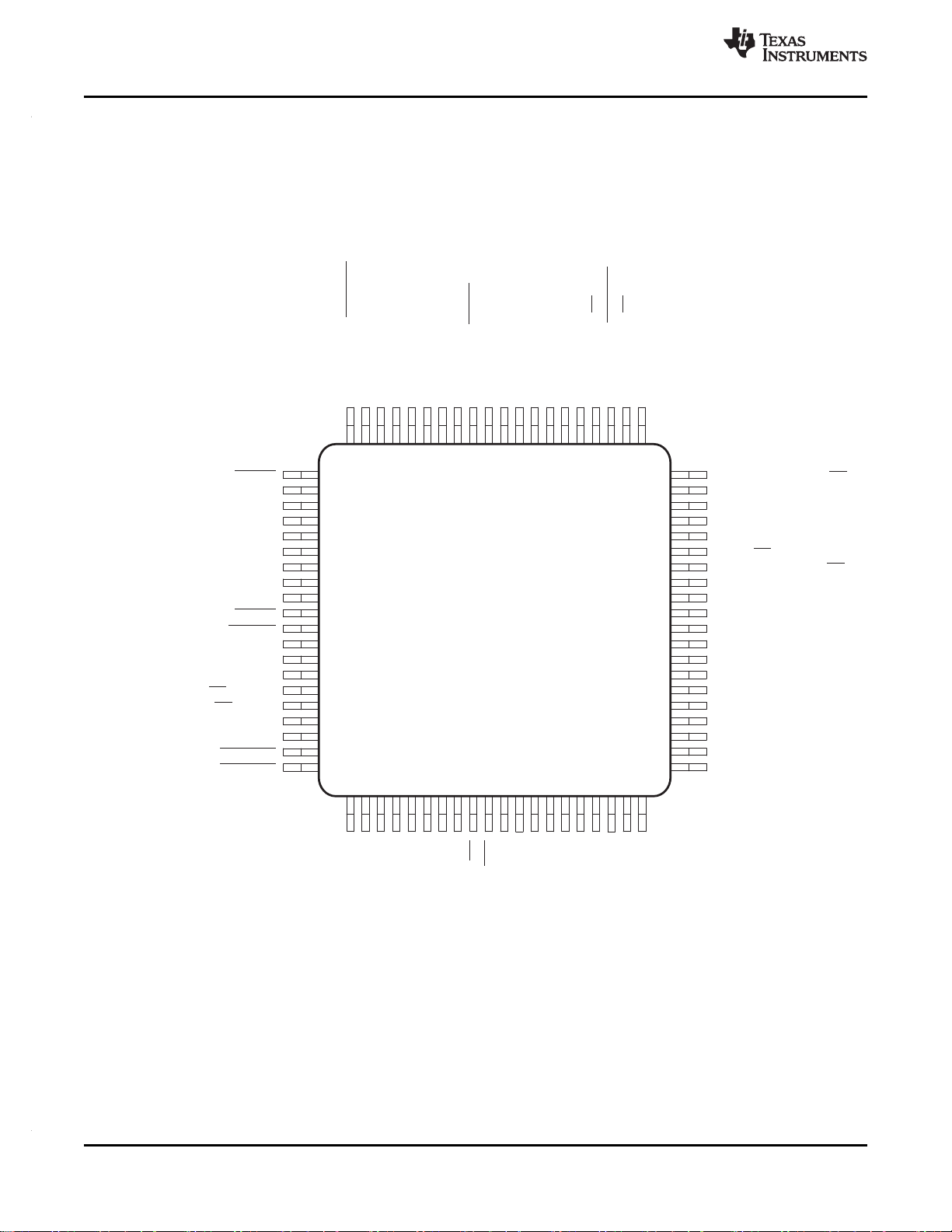
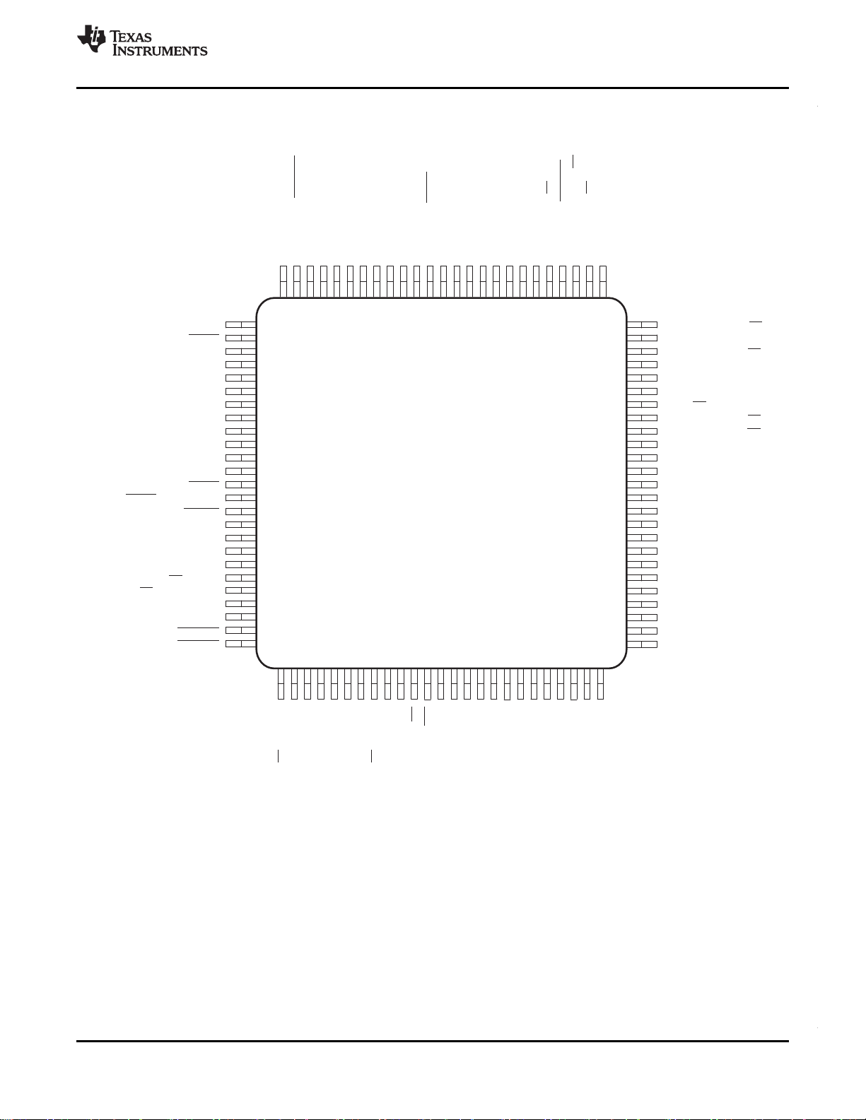
3.3 Pin Assignments
Figure 3-8 shows the 80-pin PN/PFP Low-Profile Quad Flatpack (LQFP) pin assignments. Figure 3-9
shows the 100-pin PZ/PZP Low-Profile Quad Flatpack (LQFP) pin assignments.
www.ti.com
A. Pin 19: V
one another.
Pin 21: V
and ADCINA0 share the same pin on the 80-pin PN/PFP device and their use is mutually exclusive to
REFHI
is always connected to V
REFLO
Figure 3-8. 80-Pin PN/PFP LQFP (Top View)
SSA
on the 80-pin PN/PFP device.
20 Device Overview Copyright © 2010–2011, Texas Instruments Incorporated
Submit Documentation Feedback
Product Folder Link(s): TMS320F28069 TMS320F28068 TMS320F28067 TMS320F28066 TMS320F28065
TMS320F28064 TMS320F28063 TMS320F28062
Page 21
ADVANCEINFORMATION
75
74
73
72
71
70
69
68
67
66
65
64
63
62
50
49
48
47
46
45
44
43
42
41
40
39
38
37
76
77
78
79
80
81
82
83
84
85
86
87
88
89
1
2
3
4
5
6
7
8
9
10
11
12
13
14
61
60
59
58
57
56
15
16
17
18
19
20
90
91
92
93
94
95
36
35
34
33
32
31
21
22
23
24
25
30
29
28
27
26
55
54
53
52
51
96
97
98
99
100
V
DD
V
DD
V
DD
V
DD
V
DD
V
DD
V
SS
V
SS
V
SS
V
SS
V
SS
V
SS
V
SS
V
DDIO
V
DDIO
V
DDIO
V
DDIO
V
REFHI
V
DDIO
V
DDIO
V
DD3VFL
V
SSA
TEST2
ADCINB7
ADCINB3
X1
X2
VREGENZ
V
REFLO
ADCINB6/COMP3B/AIO14
ADCINB5
ADCINB4/COMP2B/AIO12
ADCINB2/COMP1B/AIO10
ADCINB1
ADCINB0
GPIO0/EPWM1A
GPIO1/EPWM1B/COMP1OUT
GPIO2/EPWM2A
GPIO56/SPICLKA/EQEP2I/HRCAP3
GPIO57/ /EQEP2S/HRCAP4SPISTEA
GPIO58/MCLKRA/SCITXDB/EPWM7A
GPIO40/EPWM7A/SCITXDB
GPIO41/EPWM7B/SCIRXDB
GPIO3/EPWM2B/SPISOMIA/COMP2OUT
GPIO6/EPWM4A/EPWMSYNCI/EPWMSYNCO
GPIO44/MFSRA/SCIRXDB/EPWM7B
GPIO7/EPWM4B/SCIRXDA/ECAP2
GPIO8/EPWM5A/ADCSOCAO
GPIO9/EPWM5B/SCITXDB/ECAP3
GPIO10/EPWM6A/ADCSOCBO
GPIO11/EPWM6B/SCIRXDB/ECAP1
GPIO12/ /SCITXDA/SPISIMOBTZ1
GPIO13/ /SPISOMIBTZ2
GPIO14/ /SCITXDB/SPICLKBTZ3
GPIO15/ECAP2/SCIRXDB/SPISTEB
GPIO16/SPISIMOA/TZ2
GPIO17/SPISOMIA/TZ3
GPIO42/EPWM8A/ /COMP1OUTTZ1
GPIO43/EPWM8B/ /COMP2OUTTZ2
GPIO18/SPICLKA/SCITXDB/XCLKOUT
GPIO19/XCLKIN/ /SCIRXDB/ECAP1SPISTEA
GPIO22/EQEP1S/MCLKXA/SCITXDB
GPIO24/ECAP1/EQEP2A/SPISIMOB
GPIO25/ECAP2/EQEP2B/SPISOMIB
GPIO26/ECAP3/EQEP2I/SPICLKB
GPIO27/HRCAP2/EQEP2S/SPISTEB
GPIO28/SCIRXDA/SDAA/TZ2
GPIO29/SCITXDA/SCLA/TZ3
GPIO30/CANRXA/EQEP2I/EPWM7A
GPIO50/EQEP1A/MDXA/TZ1
GPIO51/EQEP1B/MDRA/TZ2
GPIO52/EQEP1S/MCLKXA/TZ3
GPIO53/EQEP1I/MFSXA
GPIO54/SPISIMOA/EQEP2A/HRCAP1
GPIO55/SPISOMIA/EQEP2B/HRCAP2
GPIO31/CANTXA/EQEP2S/EPWM8A
GPIO32/SDAA/EPWMSYNCI/ADCSOCAO
GPIO33/SCLA/EPWMSYNCO/ADCSOCBO
GPIO34/COMP2OUT/COMP3OUT
GPIO35/TDI
GPIO36/TMS
GPIO37/TDO
GPIO38/XCLKIN/TCK
GPIO39
GPIO23/EQEP1I/MFSXA/SCIRXDB
GPIO20/EQEP1A/MDXA/COMP1OUT
GPIO21/EQEP1B/MDRA/COMP2OUT
GPIO4/EPWM3A
GPIO5/EPWM3B/SPISIMOA/ECAP1
ADCINA7
ADCINA3
XRS
TRST
ADCINA6/COMP3A/AIO6
ADCINA5
ADCINA4/COMP2A/AIO4
ADCINA2/COMP1A/AIO2
ADCINA1
ADCINA0
V
DDA
www.ti.com
TMS320F28069, TMS320F28068, TMS320F28067, TMS320F28066
TMS320F28065, TMS320F28064, TMS320F28063, TMS320F28062
SPRS698A–NOVEMBER 2010–REVISED JANUARY 2011
Figure 3-9. 100-Pin PZ/PZP LQFP (Top View)
Copyright © 2010–2011, Texas Instruments Incorporated Device Overview 21
Submit Documentation Feedback
Product Folder Link(s): TMS320F28069 TMS320F28068 TMS320F28067 TMS320F28066 TMS320F28065
TMS320F28064 TMS320F28063 TMS320F28062
Page 22
ADVANCEINFORMATION
TMS320F28069, TMS320F28068, TMS320F28067, TMS320F28066
TMS320F28065, TMS320F28064, TMS320F28063, TMS320F28062
SPRS698A–NOVEMBER 2010–REVISED JANUARY 2011
3.4 Signal Descriptions
Table 3-6 describes the signals. With the exception of the JTAG pins, the GPIO function is the default at
reset, unless otherwise mentioned. The peripheral signals that are listed under them are alternate
functions. Some peripheral functions may not be available in all devices. See Table 3-1 for details. Inputs
are not 5-V tolerant. All GPIO pins are I/O/Z and have an internal pullup, which can be selectively
enabled/disabled on a per-pin basis. This feature only applies to the GPIO pins. The pullups on the PWM
pins are not enabled at reset. The pullups on other GPIO pins are enabled upon reset. The AIO pins do
not have an internal pullup.
NOTE: When the on-chip VREG is used, the GPIO19, GPIO34, GPIO35, GPIO36, GPIO37, and GPIO38
pins could glitch during power up. If this is unacceptable in an application, 1.8 V could be supplied
externally. There is no power-sequencing requirement when using an external 1.8-V supply. However, if
the 3.3-V transistors in the level-shifting output buffers of the I/O pins are powered prior to the 1.9-V
transistors, it is possible for the output buffers to turn on, causing a glitch to occur on the pin during power
up. To avoid this behavior, power the VDDpins prior to or simultaneously with the V
the VDDpins have reached 0.7 V before the V
Table 3-6. Terminal Functions
TERMINAL
NAME
TRST 12 10 I normal device operation. An external pull-down resistor is required on this pin. The
TCK See GPIO38 I See GPIO38. JTAG test clock with internal pullup. (↑)
TMS See GPIO36 I
TDI See GPIO35 I
TDO See GPIO37 O/Z register (instruction or data) are shifted out of TDO on the falling edge of TCK.
V
DD3VFL
TEST2 45 36 I/O Test Pin. Reserved for TI. Must be left unconnected.
(1) I = Input, O = Output, Z = High Impedance, OD = Open Drain, ↑ = Pullup, ↓ = Pulldown
PZ/PZP PN/PFP
PIN # PIN #
46 37 3.3-V Flash Core Power Pin. This pin should be connected to 3.3 V at all times.
I/O/Z DESCRIPTION
JTAG test reset with internal pulldown. TRST, when driven high, gives the scan system
control of the operations of the device. If this signal is not connected or driven low, the
device operates in its functional mode, and the test reset signals are ignored.
NOTE: TRST is an active-high test pin and must be maintained low at all times during
value of this resistor should be based on drive strength of the debugger pods
applicable to the design. A 2.2-kΩ resistor generally offers adequate protection. Since
this is application-specific, it is recommended that each target board be validated for
proper operation of the debugger and the application. (↓)
See GPIO36. JTAG test-mode select (TMS) with internal pullup. This serial control
input is clocked into the TAP controller on the rising edge of TCK. (↑)
See GPIO35. JTAG test data input (TDI) with internal pullup. TDI is clocked into the
selected register (instruction or data) on a rising edge of TCK. (↑)
See GPIO37. JTAG scan out, test data output (TDO). The contents of the selected
(8-mA drive)
pins reach 0.7 V.
DDIO
JTAG
FLASH
(1)
pins, ensuring that
DDIO
www.ti.com
22 Device Overview Copyright © 2010–2011, Texas Instruments Incorporated
Submit Documentation Feedback
Product Folder Link(s): TMS320F28069 TMS320F28068 TMS320F28067 TMS320F28066 TMS320F28065
TMS320F28064 TMS320F28063 TMS320F28062
Page 23
ADVANCEINFORMATION
TMS320F28069, TMS320F28068, TMS320F28067, TMS320F28066
TMS320F28065, TMS320F28064, TMS320F28063, TMS320F28062
www.ti.com
Table 3-6. Terminal Functions (continued)
TERMINAL
NAME
XCLKOUT See GPIO18 O/Z
XCLKIN I disabled by bit 13 in the CLKCTL register.
X1 60 48 I
X2 59 47 O
XRS 11 9 I/O
ADCINA7 16 – I ADC Group A, Channel 7 input
ADCINA6 17 14 I ADC Group A, Channel 6 input
COMP3A I Comparator Input 3A
AIO6 I/O Digital AIO 6
ADCINA5 18 15 I ADC Group A, Channel 5 input
ADCINA4 19 16 I ADC Group A, Channel 4 input
COMP2A I Comparator Input 2A
AIO4 I/O Digital AIO 4
ADCINA3 20 – I ADC Group A, Channel 3 input
ADCINA2 21 17 I ADC Group A, Channel 2 input
COMP1A I Comparator Input 1A
AIO2 I/O Digital AIO 2
ADCINA1 22 18 I ADC Group A, Channel 1 input
ADCINA0 23 19 I NOTE: V
PZ/PZP PN/PFP
PIN # PIN #
See GPIO19 and
GPIO38
I/O/Z DESCRIPTION
CLOCK
See GPIO18. Output clock derived from SYSCLKOUT. XCLKOUT is either the same
frequency, one-half the frequency, or one-fourth the frequency of SYSCLKOUT. This is
controlled by bits 1:0 (XCLKOUTDIV) in the XCLK register. At reset, XCLKOUT =
SYSCLKOUT/4. The XCLKOUT signal can be turned off by setting XCLKOUTDIV to 3.
The mux control for GPIO18 must also be set to XCLKOUT for this signal to propogate
to the pin.
See GPIO19 and GPIO38. External oscillator input. Pin source for the clock is
controlled by the XCLKINSEL bit in the XCLK register, GPIO38 is the default selection.
This pin feeds a clock from an external 3.3-V oscillator. In this case, the X1 pin, if
available, must be tied to GND and the on-chip crystal oscillator must be disabled via
bit 14 in the CLKCTL register. If a crystal/resonator is used, the XCLKIN path must be
NOTE: Designs that use the GPIO38/XCLKIN/TCK pin to supply an external clock for
normal device operation may need to incorporate some hooks to disable this path
during debug using the JTAG connector. This is to prevent contention with the TCK
signal, which is active during JTAG debug sessions. The zero-pin internal oscillators
may be used during this time to clock the device.
On-chip crystal-oscillator input. To use this oscillator, a quartz crystal or a ceramic
resonator must be connected across X1 and X2. In this case, the XCLKIN path must
be disabled by bit 13 in the CLKCTL register. If this pin is not used, it must be tied to
GND.
On-chip crystal-oscillator output. A quartz crystal or a ceramic resonator must be
connected across X1 and X2. If X2 is not used, it must be left unconnected.
RESET
Device Reset (in) and Watchdog Reset (out). Piccolo devices have a built-in
power-on-reset (POR) and brown-out-reset (BOR) circuitry. As such, no external
circuitry is needed to generate a reset pulse. During a power-on or brown-out condition,
this pin is driven low by the device. See Section 5.3, Electrical Characteristics, for
thresholds of the POR/BOR block. This pin is also driven low by the MCU when a
watchdog reset occurs. During watchdog reset, the XRS pin is driven low for the
watchdog reset duration of 512 OSCCLK cycles. If need be, an external circuitry may
also drive this pin to assert a device reset. In this case, it is recommended that this pin
be driven by an open-drain device. An R-C circuit must be connected to this pin for
noise immunity reasons. Regardless of the source, a device reset causes the device to
terminate execution. The program counter points to the address contained at the
location 0x3FFFC0. When reset is deactivated, execution begins at the location
designated by the program counter. The output buffer of this pin is an open-drain with
an internal pullup.
ADC, COMPARATOR, ANALOG I/O
ADC Group A, Channel 0 input.
their use is mutually exclusive to one another.
and ADCINA0 share the same pin on the 80-pin PN/PFP device and
REFHI
SPRS698A–NOVEMBER 2010–REVISED JANUARY 2011
Copyright © 2010–2011, Texas Instruments Incorporated Device Overview 23
Submit Documentation Feedback
Product Folder Link(s): TMS320F28069 TMS320F28068 TMS320F28067 TMS320F28066 TMS320F28065
TMS320F28064 TMS320F28063 TMS320F28062
Page 24
ADVANCEINFORMATION
TMS320F28069, TMS320F28068, TMS320F28067, TMS320F28066
TMS320F28065, TMS320F28064, TMS320F28063, TMS320F28062
SPRS698A–NOVEMBER 2010–REVISED JANUARY 2011
Table 3-6. Terminal Functions (continued)
TERMINAL
PZ/PZP PN/PFP
PIN # PIN #
24 19
V
NAME
REFHI
ADCINB7 35 – I ADC Group B, Channel 7 input
ADCINB6 34 27 I ADC Group B, Channel 6 input
COMP3B I Comparator Input 3B
AIO14 I/O Digital AIO 14
ADCINB5 33 26 I ADC Group B, Channel 5 input
ADCINB4 32 25 I ADC Group B, Channel 4 input
COMP2B I Comparator Input 2B
AIO12 I/O Digital AIO12
ADCINB3 31 – I ADC Group B, Channel 3 input
ADCINB2 30 24 I ADC Group B, Channel 2 input
COMP1B I Comparator Input 1B
AIO10 I/O Digital AIO 10
ADCINB1 29 23 I ADC Group B, Channel 1 input
ADCINB0 28 22 I ADC Group B, Channel 0 input
V
REFLO
V
DDA
V
SSA
V
DD
V
DD
V
DD
V
DD
V
DD
V
DD
V
DDIO
V
DDIO
V
DDIO
V
DDIO
V
DDIO
V
DDIO
V
SS
V
SS
V
SS
V
SS
V
SS
V
SS
V
SS
27 21 NOTE: V
25 20 Analog Power Pin. Tie with a 2.2-mF capacitor (typical) close to the pin.
26 21
3 2
14 12
37 29
63 51
81 65
91 72
5 4
13 11
38 30
61 49
79 63
93 74
4 3
15 13
36 28
47 38 Digital Ground Pins
62 50
80 64
92 73
I/O/Z DESCRIPTION
ADC External Reference – only used when in ADC external reference mode. See
Section 6.10.1, Analog-to-Digital Converter (ADC).
NOTE: V
their use is mutually exclusive to one another.
and ADCINA0 share the same pin on the 80-pin PN/PFP device and
REFHI
is always connected to V
REFLO
SSA
CPU AND I/O POWER
Analog Ground Pin.
NOTE: V
is always connected to V
REFLO
SSA
CPU and Logic Digital Power Pins – no supply source needed when using internal
VREG. Tie with 1.2 µF (minimum) ceramic capacitor (10% tolerance) to ground when
using internal VREG. Higher value capacitors may be used, but could impact
supply-rail ramp-up time.
Digital I/O and Flash Power Pin – Single Supply source when VREG is enabled.
www.ti.com
on the 80-pin PN/PFP device.
on the 80-pin PN/PFP device.
24 Device Overview Copyright © 2010–2011, Texas Instruments Incorporated
Submit Documentation Feedback
Product Folder Link(s): TMS320F28069 TMS320F28068 TMS320F28067 TMS320F28066 TMS320F28065
TMS320F28064 TMS320F28063 TMS320F28062
Page 25
ADVANCEINFORMATION
TMS320F28069, TMS320F28068, TMS320F28067, TMS320F28066
TMS320F28065, TMS320F28064, TMS320F28063, TMS320F28062
www.ti.com
Table 3-6. Terminal Functions (continued)
TERMINAL
NAME
VREGENZ 90 71 I Internal VREG Enable/Disable – pull low to enable VREG, pull high to disable VREG.
GPIO0 87 69 I/O/Z General-purpose input/output 0
EPWM1A O Enhanced PWM1 Output A and HRPWM channel
GPIO1 86 68 I/O/Z General-purpose input/output 1
EPWM1B O Enhanced PWM1 Output B
COMP1OUT O Direct output of Comparator 1
GPIO2 84 67 I/O/Z General-purpose input/output 2
EPWM2A O Enhanced PWM2 Output A and HRPWM channel
GPIO3 83 66 I/O/Z General-purpose input/output 3
EPWM2B O Enhanced PWM2 Output B
SPISOMIA I/O SPI-A slave out, master in
COMP2OUT O Direct output of Comparator 2
GPIO4 9 7 I/O/Z General-purpose input/output 4
EPWM3A O Enhanced PWM3 output A and HRPWM channel
GPIO5 10 8 I/O/Z General-purpose input/output 5
EPWM3B O Enhanced PWM3 output B
SPISIMOA I/O SPI-A slave in, master out
ECAP1 I/O Enhanced Capture input/output 1
GPIO6 58 46 I/O/Z General-purpose input/output 6
EPWM4A O Enhanced PWM4 output A and HRPWM channel
EPWMSYNCI I External ePWM sync pulse input
EPWMSYNCO O External ePWM sync pulse output
GPIO7 57 45 I/O/Z General-purpose input/output 7
EPWM4B O Enhanced PWM4 output B
SCIRXDA I SCI-A receive data
ECAP2 I/O Enhanced Capture input/output 2
GPIO8 54 43 I/O/Z General-purpose input/output 8
EPWM5A O Enhanced PWM5 output A and HRPWM channel
Reserved – Reserved
ADCSOCAO O ADC start-of-conversion A
(1) The GPIO function (shown in bold italics) is the default at reset. The peripheral signals that are listed under them are alternate functions.
For JTAG pins that have the GPIO functionality multiplexed, the input path to the GPIO block is always valid. The output path from the
GPIO block and the path to the JTAG block from a pin is enabled/disabled based on the condition of the TRST signal. See the
TMS320x2806x Piccolo System Control and Interrupts Reference Guide (literature number SPRUH15).
PZ/PZP PN/PFP
PIN # PIN #
I/O/Z DESCRIPTION
VOLTAGE REGULATOR CONTROL SIGNAL
GPIO AND PERIPHERAL SIGNALS
SPRS698A–NOVEMBER 2010–REVISED JANUARY 2011
(1)
Copyright © 2010–2011, Texas Instruments Incorporated Device Overview 25
Submit Documentation Feedback
Product Folder Link(s): TMS320F28069 TMS320F28068 TMS320F28067 TMS320F28066 TMS320F28065
TMS320F28064 TMS320F28063 TMS320F28062
Page 26

ADVANCEINFORMATION
TMS320F28069, TMS320F28068, TMS320F28067, TMS320F28066
TMS320F28065, TMS320F28064, TMS320F28063, TMS320F28062
SPRS698A–NOVEMBER 2010–REVISED JANUARY 2011
Table 3-6. Terminal Functions (continued)
TERMINAL
NAME
GPIO9 49 39 I/O/Z General-purpose input/output 9
EPWM5B O Enhanced PWM5 output B
SCITXDB O
ECAP3 I/O Enhanced Capture input/output 3
GPIO10 74 60 I/O/Z General-purpose input/output 10
EPWM6A O Enhanced PWM6 output A and HRPWM channel
Reserved – Reserved
ADCSOCBO O ADC start-of-conversion B
GPIO11 73 59 I/O/Z General-purpose input/output 11
EPWM6B O Enhanced PWM6 output B
SCIRXDB I
ECAP1 I/O Enhanced Capture input/output 1
GPIO12 44 35 I/O/Z General-purpose input/output 12
TZ1 I Trip Zone input 1
SCITXDA O SCI-A transmit data
SPISIMOB I/O SPI-B slave in, master out
GPIO13 95 75 I/O/Z General-purpose input/output 13
TZ2 I Trip Zone input 2
Reserved – Reserved
SPISOMIB I/O SPI-B slave out, master in
GPIO14 96 76 I/O/Z General-purpose input/output 14
TZ3 I Trip zone input 3
SCITXDB O
SPICLKB I/O SPI-B clock input/output
GPIO15 88 70 I/O/Z General-purpose input/output 15
ECAP2 I/O Enhanced Capture input/output 2
SCIRXDB I
SPISTEB I/O SPI-B slave transmit enable input/output
GPIO16 55 44 I/O/Z General-purpose input/output 16
SPISIMOA I/O SPI-A slave in, master out
Reserved – Reserved
TZ2 I Trip Zone input 2
GPIO17 52 42 I/O/Z General-purpose input/output 17
SPISOMIA I/O SPI-A slave out, master in
Reserved – Reserved
TZ3 I Trip zone input 3
PZ/PZP PN/PFP
PIN # PIN #
I/O/Z DESCRIPTION
SCI-B transmit data.
NOTE: SCI-B is only available in the PZ and PZP packages.
SCI-B receive data.
NOTE: SCI-B is only available in the PZ and PZP packages.
SCI-B transmit data.
NOTE: SCI-B is only available in the PZ and PZP packages.
SCI-B receive data.
NOTE: SCI-B is only available in the PZ and PZP packages.
www.ti.com
26 Device Overview Copyright © 2010–2011, Texas Instruments Incorporated
Submit Documentation Feedback
Product Folder Link(s): TMS320F28069 TMS320F28068 TMS320F28067 TMS320F28066 TMS320F28065
TMS320F28064 TMS320F28063 TMS320F28062
Page 27

ADVANCEINFORMATION
TMS320F28069, TMS320F28068, TMS320F28067, TMS320F28066
TMS320F28065, TMS320F28064, TMS320F28063, TMS320F28062
www.ti.com
Table 3-6. Terminal Functions (continued)
TERMINAL
NAME
GPIO18 51 41 I/O/Z General-purpose input/output 18
SPICLKA I/O SPI-A clock input/output
SCITXDB O
XCLKOUT O/Z Output clock derived from SYSCLKOUT. XCLKOUT is either the same frequency,
GPIO19 64 52 I/O/Z General-purpose input/output 19
XCLKIN I External Oscillator Input. The path from this pin to the clock block is not gated by the
SPISTEA I/O SPI-A slave transmit enable input/output
SCIRXDB I
ECAP1 I/O Enhanced Capture input/output 1
GPIO20 6 5 I/O/Z General-purpose input/output 20
EQEP1A I Enhanced QEP1 input A
MDXA O McBSP transmit serial data
COMP1OUT O Direct output of Comparator 1
GPIO21 7 6 I/O/Z General-purpose input/output 21
EQEP1B I Enhanced QEP1 input B
MDRA I McBSP receive serial data
COMP2OUT O Direct output of Comparator 2
GPIO22 98 78 I/O/Z General-purpose input/output 22
EQEP1S I/O Enhanced QEP1 strobe
MCLKXA I/O McBSP transmit clock
SCITXDB O
GPIO23 2 1 I/O/Z General-purpose input/output 23
EQEP1I I/O Enhanced QEP1 index
MFSXA I/O McBSP transmit frame synch
SCIRXDB I
GPIO24 97 77 I/O/Z General-purpose input/output 24
ECAP1 I/O Enhanced Capture input/output 1
EQEP2A I Enhanced QEP2 input A.
SPISIMOB I/O SPI-B slave in, master out
GPIO25 39 31 I/O/Z General-purpose input/output 25
ECAP2 I/O Enhanced Capture input/output 2
EQEP2B I
SPISOMIB I/O SPI-B slave out, master in
PZ/PZP PN/PFP
PIN # PIN #
I/O/Z DESCRIPTION
SCI-B transmit data.
NOTE: SCI-B is only available in the PZ and PZP packages.
one-half the frequency, or one-fourth the frequency of SYSCLKOUT. This is controlled
by bits 1:0 (XCLKOUTDIV) in the XCLK register. At reset, XCLKOUT =
SYSCLKOUT/4. The XCLKOUT signal can be turned off by setting XCLKOUTDIV to 3.
The mux control for GPIO18 must also be set to XCLKOUT for this signal to propogate
to the pin.
mux function of this pin. Care must be taken not to enable this path for clocking if it is
being used for the other peripheral functions.
SCI-B receive data.
NOTE: SCI-B is only available in the PZ and PZP packages.
SCI-B transmit data.
NOTE: SCI-B is only available in the PZ and PZP packages.
SCI-B receive data.
NOTE: SCI-B is only available in the PZ and PZP packages.
NOTE: eQEP2 is only available in the PZ and PZP packages.
Enhanced QEP2 input B.
NOTE: eQEP2 is only available in the PZ and PZP packages.
SPRS698A–NOVEMBER 2010–REVISED JANUARY 2011
Copyright © 2010–2011, Texas Instruments Incorporated Device Overview 27
Submit Documentation Feedback
Product Folder Link(s): TMS320F28069 TMS320F28068 TMS320F28067 TMS320F28066 TMS320F28065
TMS320F28064 TMS320F28063 TMS320F28062
Page 28

ADVANCEINFORMATION
TMS320F28069, TMS320F28068, TMS320F28067, TMS320F28066
TMS320F28065, TMS320F28064, TMS320F28063, TMS320F28062
SPRS698A–NOVEMBER 2010–REVISED JANUARY 2011
Table 3-6. Terminal Functions (continued)
TERMINAL
NAME
GPIO26 78 62 I/O/Z General-purpose input/output 26
ECAP3 I/O Enhanced Capture input/output 3
EQEP2I I/O
SPICLKB I/O SPI-B clock input/output
GPIO27 77 61 I/O/Z General-purpose input/output 27
HRCAP2 I High-Resolution Input Capture 2
EQEP2S I/O
SPISTEB I/O SPI-B slave transmit enable input/output
GPIO28 50 40 I/O/Z General-purpose input/output 28
SCIRXDA I SCI-A receive data
SDAA I/OD I2C data open-drain bidirectional port
TZ2 I Trip zone input 2
GPIO29 43 34 I/O/Z General-purpose input/output 29
SCITXDA O SCI-A transmit data
SCLA I/OD I2C clock open-drain bidirectional port
TZ3 I Trip zone input 3
GPIO30 41 33 I/O/Z General-purpose input/output 30
CANRXA I CAN receive
EQEP2I I/O
EPWM7A O Enhanced PWM7 Output A and HRPWM channel
GPIO31 40 32 I/O/Z General-purpose input/output 31
CANTXA O CAN transmit
EQEP2S I/O
EPWM8A O Enhanced PWM8 Output A and HRPWM channel
GPIO32 99 79 I/O/Z General-purpose input/output 32
SDAA I/OD I2C data open-drain bidirectional port
EPWMSYNCI I Enhanced PWM external sync pulse input
ADCSOCAO O ADC start-of-conversion A
GPIO33 100 80 I/O/Z General-purpose input/output 33
SCLA I/OD I2C clock open-drain bidirectional port
EPWMSYNCO O Enhanced PWM external synch pulse output
ADCSOCBO O ADC start-of-conversion B
GPIO34 68 55 I/O/Z General-purpose input/output 34
COMP2OUT O Direct output of Comparator 2
COMP3OUT O Direct output of Comparator 3
GPIO35 71 57 I/O/Z General-purpose input/output 35
TDI I JTAG test data input (TDI) with internal pullup. TDI is clocked into the selected register
GPIO36 72 58 I/O/Z General-purpose input/output 36
TMS I JTAG test-mode select (TMS) with internal pullup. This serial control input is clocked
GPIO37 70 56 I/O/Z General-purpose input/output 37
TDO O/Z JTAG scan out, test data output (TDO). The contents of the selected register
PZ/PZP PN/PFP
PIN # PIN #
I/O/Z DESCRIPTION
Enhanced QEP2 index.
NOTE: eQEP2 is only available in the PZ and PZP packages.
Enhanced QEP2 strobe.
NOTE: eQEP2 is only available in the PZ and PZP packages.
Enhanced QEP2 index.
NOTE: eQEP2 is only available in the PZ and PZP packages.
Enhanced QEP2 strobe.
NOTE: eQEP2 is only available in the PZ and PZP packages.
(instruction or data) on a rising edge of TCK.
into the TAP controller on the rising edge of TCK.
(instruction or data) are shifted out of TDO on the falling edge of TCK (8 mA drive).
www.ti.com
28 Device Overview Copyright © 2010–2011, Texas Instruments Incorporated
Submit Documentation Feedback
Product Folder Link(s): TMS320F28069 TMS320F28068 TMS320F28067 TMS320F28066 TMS320F28065
TMS320F28064 TMS320F28063 TMS320F28062
Page 29
ADVANCEINFORMATION
TMS320F28069, TMS320F28068, TMS320F28067, TMS320F28066
TMS320F28065, TMS320F28064, TMS320F28063, TMS320F28062
www.ti.com
Table 3-6. Terminal Functions (continued)
TERMINAL
NAME
GPIO38 67 54 I/O/Z General-purpose input/output 38
XCLKIN I External Oscillator Input. The path from this pin to the clock block is not gated by the
TCK I JTAG test clock with internal pullup
GPIO39 66 53 I/O/Z General-purpose input/output 39
GPIO40 82 – I/O/Z General-purpose input/output 40
EPWM7A O Enhanced PWM7 output A and HRPWM channel
SCITXDB O SCI-B transmit data
GPIO41 76 – I/O/Z General-purpose input/output 41
EPWM7B O Enhanced PWM7 output B
SCIRXDB I SCI-B receive data
GPIO42 1 – I/O/Z General-purpose input/output 42
EPWM8A O Enhanced PWM8 output A and HRPWM channel
TZ1 I Trip zone input 1
COMP1OUT O Direct output of Comparator 1
GPIO43 8 – I/O/Z General-purpose input/output 43
EPWM8B O Enhanced PWM8 output B
TZ2 I Trip zone input 2
COMP2OUT O Direct output of Comparator 2
GPIO44 56 – I/O/Z General-purpose input/output 44
MFSRA I/O McBSP receive frame synch
SCIRXDB I SCI-B receive data
EPWM7B O Enhanced PWM7 output B
GPIO50 42 – I/O/Z General-purpose input/output 50
EQEP1A I Enhanced QEP1 input A
MDXA O McBSP transmit serial data
TZ1 I Trip zone input 1
GPIO51 48 – I/O/Z General-purpose input/output 51
EQEP1B I Enhanced QEP1 input B
MDRA I McBSP receive serial data
TZ2 I Trip zone input 2
GPIO52 53 – I/O/Z General-purpose input/output 52
EQEP1S I/O Enhanced QEP1 strobe
MCLKXA I/O McBSP transmit clock
TZ3 I Trip zone input 3
GPIO53 65 – I/O/Z General-purpose input/output 53
EQEP1I I/O Enhanced QEP1 index
MFSXA I/O McBSP transmit frame synch
GPIO54 69 – I/O/Z General-purpose input/output 54
SPISIMOA I/O SPI-A slave in, master out
EQEP2A I Enhanced QEP2 input A
HRCAP1 I High-Resolution Input Capture 1
PZ/PZP PN/PFP
PIN # PIN #
I/O/Z DESCRIPTION
mux function of this pin. Care must be taken to not enable this path for clocking if it is
being used for the other functions.
SPRS698A–NOVEMBER 2010–REVISED JANUARY 2011
Copyright © 2010–2011, Texas Instruments Incorporated Device Overview 29
Submit Documentation Feedback
Product Folder Link(s): TMS320F28069 TMS320F28068 TMS320F28067 TMS320F28066 TMS320F28065
TMS320F28064 TMS320F28063 TMS320F28062
Page 30

ADVANCEINFORMATION
TMS320F28069, TMS320F28068, TMS320F28067, TMS320F28066
TMS320F28065, TMS320F28064, TMS320F28063, TMS320F28062
SPRS698A–NOVEMBER 2010–REVISED JANUARY 2011
Table 3-6. Terminal Functions (continued)
TERMINAL
NAME
GPIO55 75 – I/O/Z General-purpose input/output 55
SPISOMIA I/O SPI-A slave out, master in
EQEP2B I Enhanced QEP2 input B
HRCAP2 I High-Resolution Input Capture 2
GPIO56 85 – I/O/Z General-purpose input/output 56
SPICLKA I/O SPI-A clock input/output
EQEP2I I/O Enhanced QEP2 index
HRCAP3 I High-Resolution Input Capture 3
GPIO57 89 – I/O/Z General-purpose input/output 57
SPISTEA I/O SPI-A slave transmit enable input/output
EQEP2S I/O Enhanced QEP2 strobe
HRCAP4 I High-Resolution Input Capture 4
GPIO58 94 – I/O/Z General-purpose input/output 58
MCLKRA I/O McBSP receive clock
SCITXDB O SCI-B transmit data
EPWM7A O Enhanced PWM7 output A and HRPWM channel
PZ/PZP PN/PFP
PIN # PIN #
I/O/Z DESCRIPTION
www.ti.com
30 Device Overview Copyright © 2010–2011, Texas Instruments Incorporated
Submit Documentation Feedback
Product Folder Link(s): TMS320F28069 TMS320F28068 TMS320F28067 TMS320F28066 TMS320F28065
TMS320F28064 TMS320F28063 TMS320F28062
Page 31

ADVANCEINFORMATION
TMS320F28069, TMS320F28068, TMS320F28067, TMS320F28066
TMS320F28065, TMS320F28064, TMS320F28063, TMS320F28062
www.ti.com
3.5 Brief Descriptions
3.5.1 CPU
The 2806x (C28x) family is a member of the TMS320C2000™ microcontroller (MCU) platform. The
C28x-based controllers have the same 32-bit fixed-point architecture as existing C28x MCUs. It is a very
efficient C/C++ engine, enabling users to develop not only their system control software in a high-level
language, but also enabling development of math algorithms using C/C++. The device is as efficient at
MCU math tasks as it is at system control tasks that typically are handled by microcontroller devices. This
efficiency removes the need for a second processor in many systems. The 32 x 32-bit MAC 64-bit
processing capabilities enable the controller to handle higher numerical resolution problems efficiently.
Add to this the fast interrupt response with automatic context save of critical registers, resulting in a device
that is capable of servicing many asynchronous events with minimal latency. The device has an
8-level-deep protected pipeline with pipelined memory accesses. This pipelining enables it to execute at
high speeds without resorting to expensive high-speed memories. Special branch-look-ahead hardware
minimizes the latency for conditional discontinuities. Special store conditional operations further improve
performance.
3.5.2 Control Law Accelerator (CLA)
The C28x control law accelerator is a single-precision (32-bit) floating-point unit that extends the
capabilities of the C28x CPU by adding parallel processing. The CLA is an independent processor with its
own bus structure, fetch mechanism, and pipeline. Eight individual CLA tasks, or routines, can be
specified. Each task is started by software or a peripheral such as the ADC, an ePWM, or CPU Timer 0.
The CLA executes one task at a time to completion. When a task completes the main CPU is notified by
an interrupt to the PIE and the CLA automatically begins the next highest-priority pending task. The CLA
can directly access the ADC Result registers and the ePWM+HRPWM registers. Dedicated message
RAMs provide a method to pass additional data between the main CPU and the CLA.
SPRS698A–NOVEMBER 2010–REVISED JANUARY 2011
Copyright © 2010–2011, Texas Instruments Incorporated Device Overview 31
Submit Documentation Feedback
Product Folder Link(s): TMS320F28069 TMS320F28068 TMS320F28067 TMS320F28066 TMS320F28065
TMS320F28064 TMS320F28063 TMS320F28062
Page 32

ADVANCEINFORMATION
TMS320F28069, TMS320F28068, TMS320F28067, TMS320F28066
TMS320F28065, TMS320F28064, TMS320F28063, TMS320F28062
SPRS698A–NOVEMBER 2010–REVISED JANUARY 2011
3.5.3 Viterbi, Complex Math, CRC Unit (VCU)
The C28x VCU enhances the processing power of C2000™ devices by adding additional assembly
instructions to target complex math, Viterbi decode, and CRC calculations. The VCU instructions
accelerate many applications, including the following:
• Orthogonal frequency-division multiplex (OFDM) used in the PRIME and G3 standards for power line
communications
• Short-range radar complex math calculations
• Power calculations
• Memory and data communication packet checks (CRC)
The VCU features include:
• Instructions to support Cyclic Redundancy Checks (CRCs), which is a polynomial code checksum.
– CRC8
– CRC16
– CRC32
• Instructions to support a flexible software implementation of a Viterbi decoder
– Branch metric calculations for a code rate of 1/2 or 1/3
– Add-Compare Select or Viterbi Butterfly in 5 cycles per butterfly
– Traceback in 3 cycles per stage
– Easily supports a constraint length of K = 7 used in PRIME and G3 standards
• Complex math arithmetic unit
– Single-cycle Add or Subtract
– 2-cycle multiply
– 2-cycle multiply and accumulate (MAC)
– Single-cycle repeat MAC
• Independent register space
www.ti.com
3.5.4 Memory Bus (Harvard Bus Architecture)
As with many MCU-type devices, multiple busses are used to move data between the memories and
peripherals and the CPU. The memory bus architecture contains a program read bus, data read bus, and
data write bus. The program read bus consists of 22 address lines and 32 data lines. The data read and
write busses consist of 32 address lines and 32 data lines each. The 32-bit-wide data busses enable
single cycle 32-bit operations. The multiple bus architecture, commonly termed Harvard Bus, enables the
C28x to fetch an instruction, read a data value and write a data value in a single cycle. All peripherals and
memories attached to the memory bus prioritize memory accesses. Generally, the priority of memory bus
accesses can be summarized as follows:
Highest: Data Writes (Simultaneous data and program writes cannot occur on the
memory bus.)
Program Writes (Simultaneous data and program writes cannot occur on the
memory bus.)
Data Reads
Program Reads (Simultaneous program reads and fetches cannot occur on the
memory bus.)
Lowest: Fetches (Simultaneous program reads and fetches cannot occur on the
memory bus.)
32 Device Overview Copyright © 2010–2011, Texas Instruments Incorporated
Submit Documentation Feedback
Product Folder Link(s): TMS320F28069 TMS320F28068 TMS320F28067 TMS320F28066 TMS320F28065
TMS320F28064 TMS320F28063 TMS320F28062
Page 33

ADVANCEINFORMATION
www.ti.com
3.5.5 Peripheral Bus
To enable migration of peripherals between various Texas Instruments (TI) MCU family of devices, the
devices adopt a peripheral bus standard for peripheral interconnect. The peripheral bus bridge multiplexes
the various busses that make up the processor Memory Bus into a single bus consisting of 16 address
lines and 16 or 32 data lines and associated control signals. Three versions of the peripheral bus are
supported. One version supports only 16-bit accesses (called peripheral frame 2). Another version
supports both 16- and 32-bit accesses (called peripheral frame 1).
3.5.6 Real-Time JTAG and Analysis
The devices implement the standard IEEE 1149.1 JTAG
Additionally, the devices support real-time mode of operation allowing modification of the contents of
memory, peripheral, and register locations while the processor is running and executing code and
servicing interrupts. The user can also single step through non-time-critical code while enabling
time-critical interrupts to be serviced without interference. The device implements the real-time mode in
hardware within the CPU. This is a feature unique to the 28x family of devices, requiring no software
monitor. Additionally, special analysis hardware is provided that allows setting of hardware breakpoint or
data/address watch-points and generating various user-selectable break events when a match occurs.
These devices do not support boundary scan; however, IDCODE and BYPASS features are available if
the following considerations are taken into account. The IDCODE does not come by default. The user
needs to go through a sequence of SHIFT IR and SHIFT DR state of JTAG to get the IDCODE. For
BYPASS instruction, the first shifted DR value would be 1.
TMS320F28069, TMS320F28068, TMS320F28067, TMS320F28066
TMS320F28065, TMS320F28064, TMS320F28063, TMS320F28062
SPRS698A–NOVEMBER 2010–REVISED JANUARY 2011
(1)
interface for in-circuit based debug.
3.5.7 Flash
The F28069/68/67/66 devices contain 128K x 16 of embedded flash memory, segregated into eight
16K x 16 sectors. The F28065/64/63/62 devices contain 64K x 16 of embedded flash memory, segregated
into eight 8K x 16 sectors. All devices also contain a single 1K x 16 of OTP memory at address range
0x3D 7800 – 0x3D 7BFF. The user can individually erase, program, and validate a flash sector while
leaving other sectors untouched. However, it is not possible to use one sector of the flash or the OTP to
execute flash algorithms that erase/program other sectors. Special memory pipelining is provided to
enable the flash module to achieve higher performance. The flash/OTP is mapped to both program and
data space; therefore, it can be used to execute code or store data information. Addresses 0x3F 7FF0 –
0x3F 7FF5 are reserved for data variables and should not contain program code.
NOTE
The Flash and OTP wait-states can be configured by the application. This allows applications
running at slower frequencies to configure the flash to use fewer wait-states.
Flash effective performance can be improved by enabling the flash pipeline mode in the
Flash options register. With this mode enabled, effective performance of linear code
execution will be much faster than the raw performance indicated by the wait-state
configuration alone. The exact performance gain when using the Flash pipeline mode is
application-dependent.
For more information on the Flash options, Flash wait-state, and OTP wait-state registers,
see the TMS320x2806x Piccolo System Control and Interrupts Reference Guide (literature
number SPRUH15).
(1) IEEE Standard 1149.1-1990 Standard Test Access Port and Boundary Scan Architecture
Copyright © 2010–2011, Texas Instruments Incorporated Device Overview 33
Submit Documentation Feedback
Product Folder Link(s): TMS320F28069 TMS320F28068 TMS320F28067 TMS320F28066 TMS320F28065
TMS320F28064 TMS320F28063 TMS320F28062
Page 34

ADVANCEINFORMATION
TMS320F28069, TMS320F28068, TMS320F28067, TMS320F28066
TMS320F28065, TMS320F28064, TMS320F28063, TMS320F28062
SPRS698A–NOVEMBER 2010–REVISED JANUARY 2011
3.5.8 M0, M1 SARAMs
All devices contain these two blocks of single-access memory, each 1K x 16 in size. The stack pointer
points to the beginning of block M1 on reset. The M0 and M1 blocks, like all other memory blocks on C28x
devices, are mapped to both program and data space. Hence, the user can use M0 and M1 to execute
code or for data variables. The partitioning is performed within the linker. The C28x device presents a
unified memory map to the programmer. This makes for easier programming in high-level languages.
3.5.9 L4 SARAM, and L0, L1, L2, L3, L5, L6, L7, and L8 DPSARAMs
The device contains up to 48K x 16 of single-access RAM. To ascertain the exact size for a given device,
see the device-specific memory map figures in Section 3.2. This block is mapped to both program and
data space. L0 is 2K in size. L1 and L2 are each 1K in size. L3 is 4K in size. L4, L5, L6, L7, and L8 are
each 8K in size. L0, L1, and L2 are shared with the CLA, which can utilize these blocks for its data space.
L3 is shared with the CLA, which can utilize this block for its program space. L5, L6, L7, and L8 are
shared with the DMA, which can utilize these blocks for its data space. DPSARAM refers to the dual-port
configuration of these blocks.
3.5.10 Boot ROM
The Boot ROM is factory-programmed with boot-loading software. Boot-mode signals are provided to tell
the bootloader software what boot mode to use on power up. The user can select to boot normally or to
download new software from an external connection or to select boot software that is programmed in the
internal Flash/ROM. The Boot ROM also contains standard tables, such as SIN/COS waveforms, for use
in math-related algorithms.
Table 3-7. Boot Mode Selection
www.ti.com
MODE GPIO37/TDO TRST MODE
3 1 1 0 GetMode
2 1 0 0 Wait (see Section 3.5.11 for description)
1 0 1 0 SCI
0 0 0 0 Parallel IO
EMU x x 1 Emulation Boot
GPIO34/COMP2OUT/
COMP3OUT
3.5.10.1 Emulation Boot
When the emulator is connected, the GPIO37/TDO pin cannot be used for boot mode selection. In this
case, the boot ROM detects that an emulator is connected and uses the contents of two reserved SARAM
locations in the PIE vector table to determine the boot mode. If the content of either location is invalid,
then the Wait boot option is used. All boot mode options can be accessed in emulation boot.
3.5.10.2 GetMode
The default behavior of the GetMode option is to boot to flash. This behavior can be changed to another
boot option by programming two locations in the OTP. If the content of either OTP location is invalid, then
boot to flash is used. One of the following loaders can be specified: SCI, SPI, I2C, CAN, or OTP.
34 Device Overview Copyright © 2010–2011, Texas Instruments Incorporated
Submit Documentation Feedback
Product Folder Link(s): TMS320F28069 TMS320F28068 TMS320F28067 TMS320F28066 TMS320F28065
TMS320F28064 TMS320F28063 TMS320F28062
Page 35

ADVANCEINFORMATION
TMS320F28069, TMS320F28068, TMS320F28067, TMS320F28066
TMS320F28065, TMS320F28064, TMS320F28063, TMS320F28062
www.ti.com
3.5.10.3 Peripheral Pins Used by the Bootloader
Table 3-8 shows which GPIO pins are used by each peripheral bootloader. Refer to the GPIO mux table
to see if these conflict with any of the peripherals you would like to use in your application.
Table 3-8. Peripheral Bootload Pins
BOOTLOADER PERIPHERAL LOADER PINS
SCI SCIRXDA (GPIO28)
SCITXDA (GPIO29)
Parallel Boot Data (GPIO31,30,5:0)
28x Control (AIO6)
Host Control (AIO12)
SPI SPISIMOA (GPIO16)
SPISOMIA (GPIO17)
SPICLKA (GPIO18)
SPISTEA (GPIO19)
I2C SDAA (GPIO32)
SCLA (GPIO33)
CAN CANRXA (GPIO30)
CANTXA (GPIO31)
SPRS698A–NOVEMBER 2010–REVISED JANUARY 2011
3.5.11 Security
The devices support high levels of security to protect the user firmware from being reverse-engineered.
The security features a 128-bit password (hardcoded for 16 wait-states), which the user programs into the
flash. One code security module (CSM) is used to protect the flash/OTP and the L0/L1 SARAM blocks.
The security feature prevents unauthorized users from examining the memory contents via the JTAG port,
executing code from external memory or trying to boot-load some undesirable software that would export
the secure memory contents. To enable access to the secure blocks, the user must write the correct
128-bit KEY value that matches the value stored in the password locations within the Flash.
In addition to the CSM, the emulation code security logic (ECSL) has been implemented to prevent
unauthorized users from stepping through secure code. Any code or data access to flash, user OTP, or L0
memory while the emulator is connected will trip the ECSL and break the emulation connection. To allow
emulation of secure code, while maintaining the CSM protection against secure memory reads, the user
must write the correct value into the lower 64 bits of the KEY register, which matches the value stored in
the lower 64 bits of the password locations within the flash. Note that dummy reads of all 128 bits of the
password in the flash must still be performed. If the lower 64 bits of the password locations are all ones
(unprogrammed), then the KEY value does not need to match.
When initially debugging a device with the password locations in flash programmed (i.e., secured), the
CPU will start running and may execute an instruction that performs an access to a protected ECSL area.
If this happens, the ECSL will trip and cause the emulator connection to be cut.
Copyright © 2010–2011, Texas Instruments Incorporated Device Overview 35
Submit Documentation Feedback
Product Folder Link(s): TMS320F28069 TMS320F28068 TMS320F28067 TMS320F28066 TMS320F28065
TMS320F28064 TMS320F28063 TMS320F28062
Page 36

ADVANCEINFORMATION
TMS320F28069, TMS320F28068, TMS320F28067, TMS320F28066
TMS320F28065, TMS320F28064, TMS320F28063, TMS320F28062
SPRS698A–NOVEMBER 2010–REVISED JANUARY 2011
The solution is to use the Wait boot option. This will sit in a loop around a software breakpoint to allow an
emulator to be connected without tripping security. Piccolo devices do not support a hardware
wait-in-reset mode.
NOTE
• When the code-security passwords are programmed, all addresses between 0x3F 7F80
and 0x3F 7FF5 cannot be used as program code or data. These locations must be
programmed to 0x0000.
• If the code security feature is not used, addresses 0x3F 7F80 through 0x3F 7FEF may
be used for code or data. Addresses 0x3F 7FF0 – 0x3F 7FF5 are reserved for data and
should not contain program code.
The 128-bit password (at 0x3F 7FF8 – 0x3F 7FFF) must not be programmed to zeros. Doing
so would permanently lock the device.
Disclaimer
Code Security Module Disclaimer
THE CODE SECURITY MODULE (CSM) INCLUDED ON THIS DEVICE WAS DESIGNED
TO PASSWORD PROTECT THE DATA STORED IN THE ASSOCIATED MEMORY
(EITHER ROM OR FLASH) AND IS WARRANTED BY TEXAS INSTRUMENTS (TI), IN
ACCORDANCE WITH ITS STANDARD TERMS AND CONDITIONS, TO CONFORM TO
TI'S PUBLISHED SPECIFICATIONS FOR THE WARRANTY PERIOD APPLICABLE FOR
THIS DEVICE.
TI DOES NOT, HOWEVER, WARRANT OR REPRESENT THAT THE CSM CANNOT BE
COMPROMISED OR BREACHED OR THAT THE DATA STORED IN THE ASSOCIATED
MEMORY CANNOT BE ACCESSED THROUGH OTHER MEANS. MOREOVER, EXCEPT
AS SET FORTH ABOVE, TI MAKES NO WARRANTIES OR REPRESENTATIONS
CONCERNING THE CSM OR OPERATION OF THIS DEVICE, INCLUDING ANY IMPLIED
WARRANTIES OF MERCHANTABILITY OR FITNESS FOR A PARTICULAR PURPOSE.
IN NO EVENT SHALL TI BE LIABLE FOR ANY CONSEQUENTIAL, SPECIAL, INDIRECT,
INCIDENTAL, OR PUNITIVE DAMAGES, HOWEVER CAUSED, ARISING IN ANY WAY
OUT OF YOUR USE OF THE CSM OR THIS DEVICE, WHETHER OR NOT TI HAS BEEN
ADVISED OF THE POSSIBILITY OF SUCH DAMAGES. EXCLUDED DAMAGES INCLUDE,
BUT ARE NOT LIMITED TO LOSS OF DATA, LOSS OF GOODWILL, LOSS OF USE OR
INTERRUPTION OF BUSINESS OR OTHER ECONOMIC LOSS.
www.ti.com
3.5.12 Peripheral Interrupt Expansion (PIE) Block
The PIE block serves to multiplex numerous interrupt sources into a smaller set of interrupt inputs. The
PIE block can support up to 96 peripheral interrupts. On the F2806x, 72 of the possible 96 interrupts are
used by peripherals. The 96 interrupts are grouped into blocks of 8 and each group is fed into 1 of
12 CPU interrupt lines (INT1 to INT12). Each of the 96 interrupts is supported by its own vector stored in a
dedicated RAM block that can be overwritten by the user. The vector is automatically fetched by the CPU
on servicing the interrupt. It takes 8 CPU clock cycles to fetch the vector and save critical CPU registers.
Hence the CPU can quickly respond to interrupt events. Prioritization of interrupts is controlled in
hardware and software. Each individual interrupt can be enabled/disabled within the PIE block.
36 Device Overview Copyright © 2010–2011, Texas Instruments Incorporated
Submit Documentation Feedback
Product Folder Link(s): TMS320F28069 TMS320F28068 TMS320F28067 TMS320F28066 TMS320F28065
TMS320F28064 TMS320F28063 TMS320F28062
Page 37

ADVANCEINFORMATION
TMS320F28069, TMS320F28068, TMS320F28067, TMS320F28066
TMS320F28065, TMS320F28064, TMS320F28063, TMS320F28062
www.ti.com
3.5.13 External Interrupts (XINT1–XINT3)
The devices support three masked external interrupts (XINT1–XINT3). Each of the interrupts can be
selected for negative, positive, or both negative and positive edge triggering and can also be
enabled/disabled. These interrupts also contain a 16-bit free-running up counter, which is reset to zero
when a valid interrupt edge is detected. This counter can be used to accurately time-stamp the interrupt.
There are no dedicated pins for the external interrupts. XINT1, XINT2, and XINT3 interrupts can accept
inputs from GPIO0–GPIO31 pins.
3.5.14 Internal Zero Pin Oscillators, Oscillator, and PLL
The device can be clocked by either of the two internal zero-pin oscillators, an external oscillator, or by a
crystal attached to the on-chip oscillator circuit. A PLL is provided supporting up to 16 input-clock-scaling
ratios. The PLL ratios can be changed on-the-fly in software, enabling the user to scale back on operating
frequency if lower power operation is desired. Refer to Section 5, Electrical Specifications, for timing
details. The PLL block can be set in bypass mode. A second PLL (PLL2) feeds the HRCAP module.
3.5.15 Watchdog
Each device contains two watchdogs: CPU-Watchdog that monitors the core and NMI-Watchdog that is a
missing clock-detect circuit. The user software must regularly reset the CPU-watchdog counter within a
certain time frame; otherwise, the CPU-watchdog generates a reset to the processor. The CPU-watchdog
can be disabled if necessary. The NMI-Watchdog engages only in case of a clock failure and can either
generate an interrupt or a device reset.
SPRS698A–NOVEMBER 2010–REVISED JANUARY 2011
3.5.16 Peripheral Clocking
The clocks to each individual peripheral can be enabled/disabled to reduce power consumption when a
peripheral is not in use. Additionally, the system clock to the serial ports (except I2C) can be scaled
relative to the CPU clock.
3.5.17 Low-power Modes
The devices are full static CMOS devices. Three low-power modes are provided:
IDLE: Places CPU in low-power mode. Peripheral clocks may be turned off selectively and
only those peripherals that need to function during IDLE are left operating. An
enabled interrupt from an active peripheral or the watchdog timer will wake the
processor from IDLE mode.
STANDBY: Turns off clock to CPU and peripherals. This mode leaves the oscillator and PLL
functional. An external interrupt event will wake the processor and the peripherals.
Execution begins on the next valid cycle after detection of the interrupt event
HALT: This mode basically shuts down the device and places it in the lowest possible
power-consumption mode. If the internal zero-pin oscillators are used as the clock
source, the HALT mode turns them off, by default. To keep these oscillators from
shutting down, the INTOSCnHALTI bits in CLKCTL register may be used. The
zero-pin oscillators may thus be used to clock the CPU-watchdog in this mode. If the
on-chip crystal oscillator is used as the clock source, it is shut down in this mode. A
reset or an external signal (through a GPIO pin) or the CPU-watchdog can wake the
device from this mode.
The CPU clock (OSCCLK) and WDCLK should be from the same clock source before attempting to put
the device into HALT or STANDBY.
Copyright © 2010–2011, Texas Instruments Incorporated Device Overview 37
Submit Documentation Feedback
Product Folder Link(s): TMS320F28069 TMS320F28068 TMS320F28067 TMS320F28066 TMS320F28065
TMS320F28064 TMS320F28063 TMS320F28062
Page 38

ADVANCEINFORMATION
TMS320F28069, TMS320F28068, TMS320F28067, TMS320F28066
TMS320F28065, TMS320F28064, TMS320F28063, TMS320F28062
SPRS698A–NOVEMBER 2010–REVISED JANUARY 2011
3.5.18 Peripheral Frames 0, 1, 2, 3 (PFn)
The device segregates peripherals into four sections. The mapping of peripherals is as follows:
PF0: PIE: PIE Interrupt Enable and Control Registers Plus PIE Vector Table
Flash: Flash Waitstate Registers
Timers: CPU-Timers 0, 1, 2 Registers
CSM: Code Security Module KEY Registers
ADC: ADC Result Registers
CLA: Control Law Accelrator Registers and Message RAMs
PF1: GPIO: GPIO MUX Configuration and Control Registers
eCAN: Enhanced Control Area Network Configuration and Control Registers
ePWM: Enhanced Pulse Width Modulator Module and Registers
eCAP: Enhanced Capture Module and Registers
eQEP: Enhanced Quadrature Encoder Pulse Module and Registers
Comparators: Comparator Modules
PF2: SYS: System Control Registers
SCI: Serial Communications Interface (SCI) Control and RX/TX Registers
SPI: Serial Port Interface (SPI) Control and RX/TX Registers
ADC: ADC Status, Control, and Configuration Registers
I2C: Inter-Integrated Circuit Module and Registers
XINT: External Interrupt Registers
PF3: McBSP: Multichannel Buffered Serial Port Registers
www.ti.com
3.5.19 General-Purpose Input/Output (GPIO) Multiplexer
Most of the peripheral signals are multiplexed with general-purpose input/output (GPIO) signals. This
enables the user to use a pin as GPIO if the peripheral signal or function is not used. On reset, GPIO pins
are configured as inputs. The user can individually program each pin for GPIO mode or peripheral signal
mode. For specific inputs, the user can also select the number of input qualification cycles. This is to filter
unwanted noise glitches. The GPIO signals can also be used to bring the device out of specific low-power
modes.
3.5.20 32-Bit CPU-Timers (0, 1, 2)
CPU-Timers 0, 1, and 2 are identical 32-bit timers with presettable periods and with 16-bit clock
prescaling. The timers have a 32-bit count-down register, which generates an interrupt when the counter
reaches zero. The counter is decremented at the CPU clock speed divided by the prescale value setting.
When the counter reaches zero, it is automatically reloaded with a 32-bit period value.
CPU-Timer 0 is for general use and is connected to the PIE block. CPU-Timer 1 is also for general use
and can be connected to INT13 of the CPU. CPU-Timer 2 is reserved for DSP/BIOS. It is connected to
INT14 of the CPU. If DSP/BIOS is not being used, CPU-Timer 2 is available for general use.
CPU-Timer 2 can be clocked by any one of the following:
• SYSCLKOUT (default)
• Internal zero-pin oscillator 1 (INTOSC1)
• Internal zero-pin oscillator 2 (INTSOC2)
• External clock source
38 Device Overview Copyright © 2010–2011, Texas Instruments Incorporated
Submit Documentation Feedback
Product Folder Link(s): TMS320F28069 TMS320F28068 TMS320F28067 TMS320F28066 TMS320F28065
TMS320F28064 TMS320F28063 TMS320F28062
Page 39

ADVANCEINFORMATION
www.ti.com
3.5.21 Control Peripherals
The devices support the following peripherals that are used for embedded control and communication:
ePWM: The enhanced PWM peripheral supports independent/complementary PWM
generation, adjustable dead-band generation for leading/trailing edges,
latched/cycle-by-cycle trip mechanism. Some of the PWM pins support the
HRPWM high resolution duty and period features. The type 1 module found on
2806x devices also supports increased dead-band resolution, enhanced SOC and
interrupt generation, and advanced triggering including trip functions based on
comparator outputs.
eCAP: The enhanced capture peripheral uses a 32-bit time base and registers up to four
programmable events in continuous/one-shot capture modes.
This peripheral can also be configured to generate an auxiliary PWM signal.
eQEP: The enhanced QEP peripheral uses a 32-bit position counter, supports low-speed
measurement using capture unit and high-speed measurement using a 32-bit unit
timer. This peripheral has a watchdog timer to detect motor stall and input error
detection logic to identify simultaneous edge transition in QEP signals.
ADC: The ADC block is a 12-bit converter. It has up to 13 single-ended channels pinned
out, depending on the device. It contains two sample-and-hold units for
simultaneous sampling.
Comparator: Each comparator block consists of one analog comparator along with an internal
10-bit reference for supplying one input of the comparator.
TMS320F28069, TMS320F28068, TMS320F28067, TMS320F28066
TMS320F28065, TMS320F28064, TMS320F28063, TMS320F28062
SPRS698A–NOVEMBER 2010–REVISED JANUARY 2011
3.5.22 Serial Port Peripherals
The devices support the following serial communication peripherals:
SPI: The SPI is a high-speed, synchronous serial I/O port that allows a serial bit stream
of programmed length (one to sixteen bits) to be shifted into and out of the device
at a programmable bit-transfer rate. Normally, the SPI is used for communications
between the MCU and external peripherals or another processor. Typical
applications include external I/O or peripheral expansion through devices such as
shift registers, display drivers, and ADCs. Multi-device communications are
supported by the master/slave operation of the SPI. The SPI contains a 4-level
receive and transmit FIFO for reducing interrupt servicing overhead.
SCI: The serial communications interface is a two-wire asynchronous serial port,
commonly known as UART. The SCI contains a 4-level receive and transmit FIFO
for reducing interrupt servicing overhead.
I2C: The inter-integrated circuit (I2C) module provides an interface between a MCU
and other devices compliant with Philips Semiconductors Inter-IC bus (I2C-bus)
specification version 2.1 and connected by way of an I2C-bus. External
components attached to this 2-wire serial bus can transmit/receive up to 8-bit data
to/from the MCU through the I2C module. The I2C contains a 4-level
receive-and-transmit FIFO for reducing interrupt servicing overhead.
eCAN: This is the enhanced version of the CAN peripheral. It supports 32 mailboxes, time
stamping of messages, and is CAN 2.0B-compliant.
McBSP: The multichannel buffered serial port (McBSP) connects to E1/T1 lines,
phone-quality codecs for modem applications or high-quality stereo audio DAC
devices. The McBSP receive and transmit registers are supported by the DMA to
significantly reduce the overhead for servicing this peripheral. Each McBSP
module can be configured as an SPI as required.
Copyright © 2010–2011, Texas Instruments Incorporated Device Overview 39
Submit Documentation Feedback
Product Folder Link(s): TMS320F28069 TMS320F28068 TMS320F28067 TMS320F28066 TMS320F28065
TMS320F28064 TMS320F28063 TMS320F28062
Page 40

ADVANCEINFORMATION
TMS320F28069, TMS320F28068, TMS320F28067, TMS320F28066
TMS320F28065, TMS320F28064, TMS320F28063, TMS320F28062
SPRS698A–NOVEMBER 2010–REVISED JANUARY 2011
3.6 Register Map
The devices contain four peripheral register spaces. The spaces are categorized as follows:
Peripheral Frame 0: These are peripherals that are mapped directly to the CPU memory bus.
See Table 3-9.
Peripheral Frame 1: These are peripherals that are mapped to the 32-bit peripheral bus. See
Table 3-10.
Peripheral Frame 2: These are peripherals that are mapped to the 16-bit peripheral bus. See
Table 3-11.
Peripheral Frame 3: McBSP registers are mapped to this. See Table 3-12.
www.ti.com
Table 3-9. Peripheral Frame 0 Registers
NAME ADDRESS RANGE SIZE (×16) EALLOW PROTECTED
Device Emulation Registers 0x00 0880 – 0x00 0984 261 Yes
System Power Control Registers 0x00 0985 – 0x00 0987 3 Yes
FLASH Registers
Code Security Module Registers 0x00 0AE0 – 0x00 0AEF 16 Yes
ADC registers 0x00 0B00 – 0x00 0B0F 16 No
(0 wait read only)
CPU–TIMER0/1/2 Registers 0x00 0C00 – 0x00 0C3F 64 No
PIE Registers 0x00 0CE0 – 0x00 0CFF 32 No
PIE Vector Table 0x00 0D00 – 0x00 0DFF 256 No
DMA Registers 0x00 1000 – 0x00 11FF 512 Yes
CLA Registers 0x00 1400 – 0x00 147F 128 Yes
CLA to CPU Message RAM (CPU writes ignored) 0x00 1480 – 0x00 14FF 128 NA
CPU to CLA Message RAM (CLA writes ignored) 0x00 1500 – 0x00 157F 128 NA
(1) Registers in Frame 0 support 16-bit and 32-bit accesses.
(2) If registers are EALLOW protected, then writes cannot be performed until the EALLOW instruction is executed. The EDIS instruction
disables writes to prevent stray code or pointers from corrupting register contents.
(3) The Flash Registers are also protected by the Code Security Module (CSM).
(3)
0x00 0A80 – 0x00 0ADF 96 Yes
(1)
(2)
40 Device Overview Copyright © 2010–2011, Texas Instruments Incorporated
Submit Documentation Feedback
Product Folder Link(s): TMS320F28069 TMS320F28068 TMS320F28067 TMS320F28066 TMS320F28065
TMS320F28064 TMS320F28063 TMS320F28062
Page 41
ADVANCEINFORMATION
TMS320F28069, TMS320F28068, TMS320F28067, TMS320F28066
TMS320F28065, TMS320F28064, TMS320F28063, TMS320F28062
www.ti.com
Table 3-10. Peripheral Frame 1 Registers
NAME ADDRESS RANGE SIZE (×16) EALLOW PROTECTED
eCAN-A registers 0x00 6000 – 0x00 61FF 512
Comparator 1 registers 0x00 6400 – 0x00 641F 32
Comparator 2 registers 0x00 6420 – 0x00 643F 32
Comparator 3 registers 0x00 6440 – 0x00 645F 32
ePWM1 + HRPWM1 registers 0x00 6800 – 0x00 683F 64
ePWM2 + HRPWM2 registers 0x00 6840 – 0x00 687F 64
ePWM3 + HRPWM3 registers 0x00 6880 – 0x00 68BF 64
ePWM4 + HRPWM4 registers 0x00 68C0 – 0x00 68FF 64
ePWM5 + HRPWM5 registers 0x00 6900 – 0x00 693F 64
ePWM6 + HRPWM6 registers 0x00 6940 – 0x00 697F 64
ePWM7 + HRPWM7 registers 0x00 6980 – 0x00 69BF 64
ePWM8 + HRPWM8 registers 0x00 69C0 – 0x00 69FF 64
eCAP1 registers 0x00 6A00 – 0x00 6A1F 32 No
eCAP2 registers 0x00 6A20 – 0x00 6A3F 32 No
eCAP3 registers 0x00 6A40 – 0x00 6A57 32 No
HRCAP1 registers 0x00 6AC0 – 0x00 6ADF 32
HRCAP2 registers 0x00 6AE0 – 0x00 6AFF 32
eQEP1 registers 0x00 6B00 – 0x00 6B3F 64
eQEP2 registers 0x00 6B40 – 0x00 6B7F 64
HRCAP3 registers 0x00 6C80 – 0x00 6C9F 32
HRCAP4 registers 0x00 6CA0 – 0x00 6CBF 32
GPIO registers 0x00 6F80 – 0x00 6FFF 128
(1) Some registers are EALLOW protected. See the module reference guide for more information.
SPRS698A–NOVEMBER 2010–REVISED JANUARY 2011
(1)
(1)
(1)
(1)
(1)
(1)
(1)
(1)
(1)
(1)
(1)
(1)
(1)
(1)
(1)
(1)
(1)
(1)
(1)
Table 3-11. Peripheral Frame 2 Registers
NAME ADDRESS RANGE SIZE (×16) EALLOW PROTECTED
System Control Registers 0x00 7010 – 0x00 702F 32 Yes
SPI-A Registers 0x00 7040 – 0x00 704F 16 No
SCI-A Registers 0x00 7050 – 0x00 705F 16 No
NMI Watchdog Interrupt Registers 0x00 7060 – 0x00 706F 16 Yes
External Interrupt Registers 0x00 7070 – 0x00 707F 16 Yes
ADC Registers 0x00 7100 – 0x00 717F 128
SPI-B Registers 0x00 7740 – 0x00 774F 16 No
SCI-B Registers 0x00 7750 – 0x00 775F 16 No
I2C-A Registers 0x00 7900 – 0x00 793F 64
(1) Some registers are EALLOW protected. See the module reference guide for more information.
Table 3-12. Peripheral Frame 3 Registers
NAME ADDRESS RANGE SIZE (×16) EALLOW PROTECTED
McBSP-A Registers 0x00 5000 – 0x00 503F 64 No
(1)
(1)
Copyright © 2010–2011, Texas Instruments Incorporated Device Overview 41
Submit Documentation Feedback
Product Folder Link(s): TMS320F28069 TMS320F28068 TMS320F28067 TMS320F28066 TMS320F28065
TMS320F28064 TMS320F28063 TMS320F28062
Page 42

ADVANCEINFORMATION
TMS320F28069, TMS320F28068, TMS320F28067, TMS320F28066
TMS320F28065, TMS320F28064, TMS320F28063, TMS320F28062
SPRS698A–NOVEMBER 2010–REVISED JANUARY 2011
3.7 Device Emulation Registers
These registers are used to control the protection mode of the C28x CPU and to monitor some critical
device signals. The registers are defined in Table 3-13.
Table 3-13. Device Emulation Registers
www.ti.com
NAME SIZE (x16) DESCRIPTION
DEVICECNF 2 Device Configuration Register Yes
PARTID 0x3D 7E80 1 Part ID Register TMS320F28069PZP/PZ 0x009E
CLASSID 0x0882 1 Class ID Register TMS320F28069 0x009F
REVID 0x0883 1 Revision ID
ADDRESS EALLOW
RANGE PROTECTED
0x0880–
0x0881
TMS320F28069PFP/PN 0x009C
TMS320F28068PZP/PZ 0x008E
TMS320F28068PFP/PN 0x008C
TMS320F28067PZP/PZ 0x008A
TMS320F28067PFP/PN 0x0088
TMS320F28066PZP/PZ 0x0086
Register
TMS320F28066PFP/PN 0x0084
TMS320F28065PZP/PZ 0x007E
TMS320F28065PFP/PN 0x007C
TMS320F28064PZP/PZ 0x006E
TMS320F28064PFP/PN 0x006C
TMS320F28063PZP/PZ 0x006A
TMS320F28063PFP/PN 0x0068
TMS320F28062PZP/PZ 0x0066
TMS320F28062PFP/PN 0x0064
TMS320F28068 0x008F
TMS320F28067 0x008F
TMS320F28066 0x008F
TMS320F28065 0x007F
TMS320F28064 0x006F
TMS320F28063 0x006F
TMS320F28062 0x006F
0x0000 - Silicon Rev. 0 - TMX No
No
No
42 Device Overview Copyright © 2010–2011, Texas Instruments Incorporated
Submit Documentation Feedback
Product Folder Link(s): TMS320F28069 TMS320F28068 TMS320F28067 TMS320F28066 TMS320F28065
TMS320F28064 TMS320F28063 TMS320F28062
Page 43

ADVANCEINFORMATION
TMS320F28069, TMS320F28068, TMS320F28067, TMS320F28066
TMS320F28065, TMS320F28064, TMS320F28063, TMS320F28062
www.ti.com
3.8 VREG/BOR/POR
Although the core and I/O circuitry operate on two different voltages, these devices have an on-chip
voltage regulator (VREG) to generate the VDDvoltage from the V
space of a second external regulator on an application board. Additionally, internal power-on reset (POR)
and brown-out reset (BOR) circuits monitor both the VDDand V
3.8.1 On-chip Voltage Regulator (VREG)
SPRS698A–NOVEMBER 2010–REVISED JANUARY 2011
supply. This eliminates the cost and
DDIO
rails during power-up and run mode.
DDIO
A linear regulator generates the core voltage (VDD) from the V
supply. Therefore, although capacitors
DDIO
are required on each VDDpin to stabilize the generated voltage, power need not be supplied to these pins
to operate the device. Conversely, the VREG can be disabled, should power or redundancy be the
primary concern of the application.
3.8.1.1 Using the On-chip VREG
To utilize the on-chip VREG, the VREGENZ pin should be tied low and the appropriate recommended
operating voltage should be supplied to the V
DDIO
and V
pins. In this case, the VDDvoltage needed by
DDA
the core logic will be generated by the VREG. Each VDDpin requires on the order of 1.2 mF (minimum)
capacitance for proper regulation of the VREG. These capacitors should be located as close as possible
to the VDDpins.
3.8.1.2 Disabling the On-chip VREG
To conserve power, it is also possible to disable the on-chip VREG and supply the core logic voltage to
the VDDpins with a more efficient external regulator. To enable this option, the VREGENZ pin must be tied
high.
3.8.2 On-chip Power-On Reset (POR) and Brown-Out Reset (BOR) Circuit
Two on-chip supervisory circuits, the power-on reset (POR) and the brown-out reset (BOR) remove the
burden of monitoring the VDDand V
to create a clean reset throughout the device during the entire power-up procedure. The trip point is a
looser, lower trip point than the BOR, which watches for dips in the VDDor V
operation. The POR function is present on both VDDand V
power-up, the BOR function is present on V
enabled (VREGENZ pin is tied low). Both functions tie the XRS pin low when one of the voltages is below
their respective trip point. Additionally, when the internal voltage regulator is enabled, an over-voltage
protection circuit will tie XRS low if the VDDrail rises above its trip point. See Section 5 for the various trip
points as well as the delay time for the device to release the XRS pin after the under/over-voltage
condition is removed. Figure 3-10 shows the VREG, POR, and BOR. To disable both the VDDand V
BOR functions, a bit is provided in the BORCFG register. Refer to the TMS320x2806x Piccolo System
Control and Interrupts Reference Guide (literature number SPRUH15) for details.
supply rails from the application board. The purpose of the POR is
DDIO
rails at all times. After initial device
DDIO
at all times, and on VDDwhen the internal VREG is
DDIO
rail during device
DDIO
DDIO
Copyright © 2010–2011, Texas Instruments Incorporated Device Overview 43
Submit Documentation Feedback
Product Folder Link(s): TMS320F28069 TMS320F28068 TMS320F28067 TMS320F28066 TMS320F28065
TMS320F28064 TMS320F28063 TMS320F28062
Page 44

ADVANCEINFORMATION
I/O Pin
In
Out
DIR (0 = Input, 1 = Output)
(Force Hi-Z When High)
SYSRS
C28
Core
Sync
RS
XRS
PLL
+
Clocking
Logic
MCLKRS
VREGHALT
Deglitch
Filter
On-Chip
Voltage
Regulator
(VREG)
VREGENZ
POR/BOR
Generating
Module
XRS
Pin
SYSCLKOUT
WDRST
(A)
JTAG
TCK
Detect
Logic
PBRS
(B)
Internal
Weak PU
TMS320F28069, TMS320F28068, TMS320F28067, TMS320F28066
TMS320F28065, TMS320F28064, TMS320F28063, TMS320F28062
SPRS698A–NOVEMBER 2010–REVISED JANUARY 2011
www.ti.com
A. WDRST is the reset signal from the CPU-watchdog.
B. PBRS is the reset signal from the POR/BOR module.
Figure 3-10. VREG + POR + BOR + Reset Signal Connectivity
44 Device Overview Copyright © 2010–2011, Texas Instruments Incorporated
Product Folder Link(s): TMS320F28069 TMS320F28068 TMS320F28067 TMS320F28066 TMS320F28065
TMS320F28064 TMS320F28063 TMS320F28062
Submit Documentation Feedback
Page 45

ADVANCEINFORMATION
TMS320F28069, TMS320F28068, TMS320F28067, TMS320F28066
TMS320F28065, TMS320F28064, TMS320F28063, TMS320F28062
www.ti.com
3.9 System Control
This section describes the oscillator and clocking mechanisms, the watchdog function and the low power
modes.
Table 3-14. PLL, Clocking, Watchdog, and Low-Power Mode Registers
NAME ADDRESS SIZE (x16) DESCRIPTION
BORCFG 0x00 0985 1 BOR Configuration Register
XCLK 0x00 7010 1 XCLKOUT Control
PLLSTS 0x00 7011 1 PLL Status Register
CLKCTL 0x00 7012 1 Clock Control Register
PLLLOCKPRD 0x00 7013 1 PLL Lock Period
INTOSC1TRIM 0x00 7014 1 Internal Oscillator 1 Trim Register
INTOSC2TRIM 0x00 7016 1 Internal Oscillator 2 Trim Register
PCLKCR2 0x00 7019 1 Peripheral Clock Control Register 2
LOSPCP 0x00 701B 1 Low-Speed Peripheral Clock Prescaler Register
PCLKCR0 0x00 701C 1 Peripheral Clock Control Register 0
PCLKCR1 0x00 701D 1 Peripheral Clock Control Register 1
LPMCR0 0x00 701E 1 Low Power Mode Control Register 0
PCLKCR3 0x00 7020 1 Peripheral Clock Control Register 3
PLLCR 0x00 7021 1 PLL Control Register
SCSR 0x00 7022 1 System Control and Status Register
WDCNTR 0x00 7023 1 Watchdog Counter Register
WDKEY 0x00 7025 1 Watchdog Reset Key Register
WDCR 0x00 7029 1 Watchdog Control Register
PLL2CTL 0x00 7030 1 PLL2 Configuration Register
PLL2MULT 0x00 7032 1 PLL2 Multiplier Register
PLL2STS 0x00 7034 1 PLL2 Lock Status Register
SYSCLK2CNTR 0x00 7036 1 SYSCLK2 Clock Counter Register
EPWMCFG 0x00 703A 1 ePWM DMA/CLA Configuration Register
(1) All registers in this table are EALLOW protected.
SPRS698A–NOVEMBER 2010–REVISED JANUARY 2011
(1)
Copyright © 2010–2011, Texas Instruments Incorporated Device Overview 45
Submit Documentation Feedback
Product Folder Link(s): TMS320F28069 TMS320F28068 TMS320F28067 TMS320F28066 TMS320F28065
TMS320F28064 TMS320F28063 TMS320F28062
Page 46

ADVANCEINFORMATION
GPIO
Mux
PCLKCR0/1/2/3
(System Ctrl Regs)
LOSPCP
(System Ctrl Regs)
Peripheral
Registers
SPI-A, SPI-B, SCI-A, SCI-B
I/O
PF2
Clock Enables LSPCLK
SYSCLKOUT
Clock Enables
C28x Core
CLKIN
LOSPCP
(System Ctrl Regs)
Peripheral
Registers
McBSP
I/O
PF3
LSPCLK
Clock Enables
Peripheral
Registers
eCAN-AI/O
PF1
Clock Enables
Peripheral
Registers
eCAP1, eCAP2, eCAP3
eQEP1, eQEP2
I/O
PF1
Clock Enables
Clock Enables
Peripheral
Registers
ePWM1, ePWM2,
ePWM3, ePWM4, ePWM5,
ePWM6, ePWM7, ePWM8
I/O
PF1
Clock Enables
Clock EnablesClock Enables
Peripheral
Registers
I2C-A
I/O
PF2
Clock Enables
Peripheral
Registers
HRCAP1, HRCAP2,
HRCAP3, HRCAP4
I/O
PF1
Clock Enables
ADC
Registers
12-Bit ADC
16 Ch
PF2
PF0
Clock Enables
COMP
Registers
COMP1/2/3
PF1
Clock Enables
6
Analog
GPIO
Mux
/2
TMS320F28069, TMS320F28068, TMS320F28067, TMS320F28066
TMS320F28065, TMS320F28064, TMS320F28063, TMS320F28062
SPRS698A–NOVEMBER 2010–REVISED JANUARY 2011
Figure 3-11 shows the various clock domains that are discussed. Figure 3-12 shows the various clock
sources (both internal and external) that can provide a clock for device operation.
www.ti.com
A. CLKIN is the clock into the CPU. It is passed out of the CPU as SYSCLKOUT (that is, CLKIN is the same frequency
as SYSCLKOUT).
Figure 3-11. Clock and Reset Domains
46 Device Overview Copyright © 2010–2011, Texas Instruments Incorporated
Product Folder Link(s): TMS320F28069 TMS320F28068 TMS320F28067 TMS320F28066 TMS320F28065
Submit Documentation Feedback
TMS320F28064 TMS320F28063 TMS320F28062
Page 47

ADVANCEINFORMATION
INTOSC1TRIM Reg
(A)
Internal
OSC 1
(10 MHz)
OSCE
CLKCTL[INTOSC1OFF]
WAKEOSC
CLKCTL[INTOSC1HALT]
INTOSC2TRIM Reg
(A)
Internal
OSC 2
(10 MHz)
OSCE
CLKCTL[INTOSC2OFF]
CLKCTL[INTOSC2HALT]
1 = Turn OSC Off
1 = Ignore HALT
1 = Turn OSC Off
1 = Ignore HALT
XCLK[XCLKINSEL]
0 = GPIO38
1 = GPIO19
GPIO19
or
GPIO38
CLKCTL[XCLKINOFF]
0
0
1
(Crystal)
OSC
XCLKIN
X1
X2
CLKCTL[XTALOSCOFF]
0 = OSC on (default on reset)
1 = Turn OSC off
0
1
0
1
OSC1CLK
OSCCLKSRC1
WDCLK
OSC2CLK
0
1
CLKCTL[WDCLKSRCSEL]
(OSC1CLK on reset)XRS
CLKCTL[OSCCLKSRCSEL]
CLKCTL[TRM2CLKPRESCALE]
CLKCTL[TMR2CLKSRCSEL]
OSCCLKSRC2
11
Prescale
/1, /2, /4,
/8, /16
00
01, 10, 11
CPUTMR2CLK
SYNC
Edge
Detect
10
01
CLKCTL[OSCCLKSRC2SEL]
SYSCLKOUT
WAKEOSC
(Oscillators enabled when this signal is high)
EXTCLK
XTAL
XCLKIN
(OSC1CLK on reset)XRS
OSCCLK
PLL
Missing-Clock-Detect Circuit
(B)
CPU-Watchdog
www.ti.com
TMS320F28069, TMS320F28068, TMS320F28067, TMS320F28066
TMS320F28065, TMS320F28064, TMS320F28063, TMS320F28062
SPRS698A–NOVEMBER 2010–REVISED JANUARY 2011
A. Register loaded from TI OTP-based calibration function.
B. See Section 3.9.4 for details on missing clock detection.
Figure 3-12. Clock Tree
Copyright © 2010–2011, Texas Instruments Incorporated Device Overview 47
Product Folder Link(s): TMS320F28069 TMS320F28068 TMS320F28067 TMS320F28066 TMS320F28065
Submit Documentation Feedback
TMS320F28064 TMS320F28063 TMS320F28062
Page 48
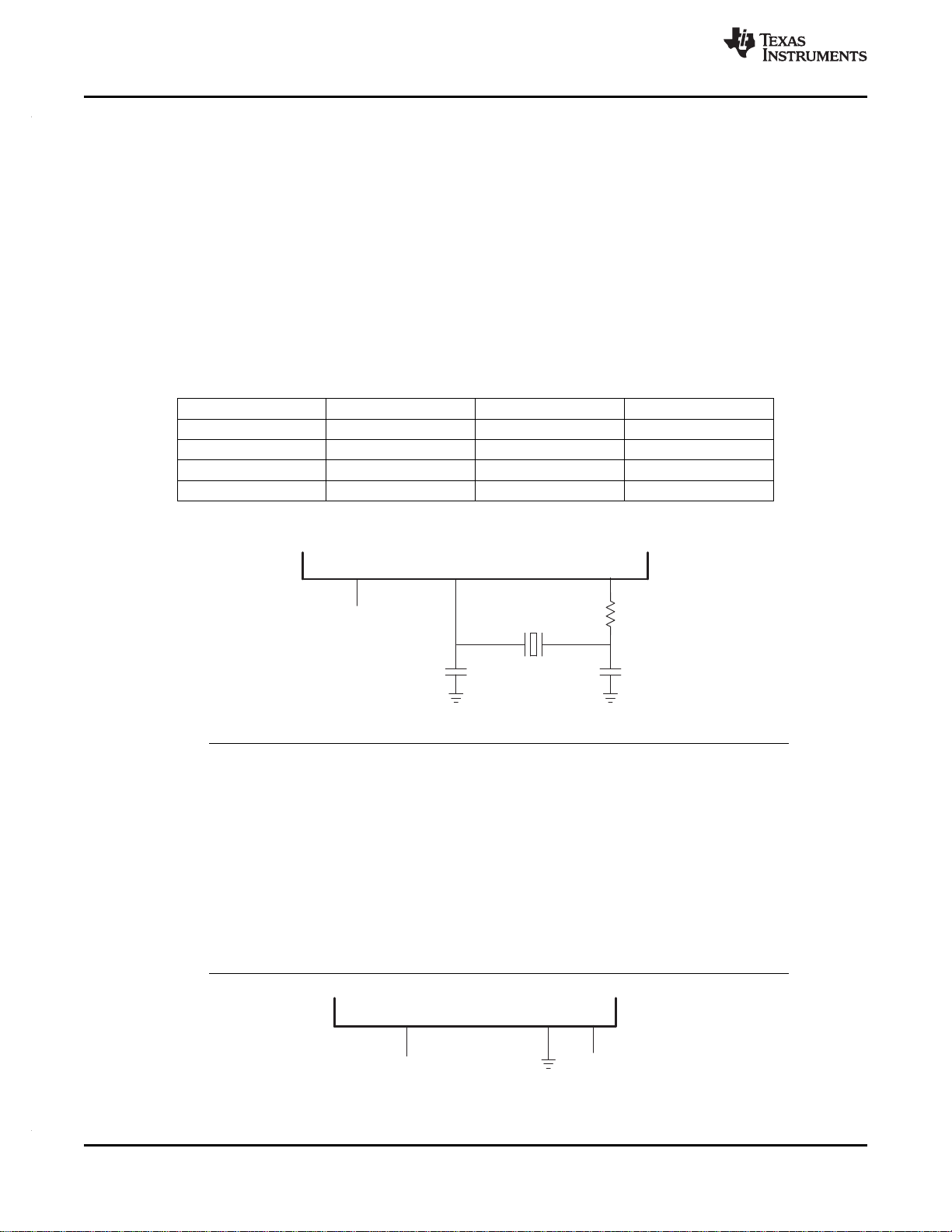
ADVANCEINFORMATION
X2X1
Crystal
XCLKIN/GPIO19/38
Turn off
XCLKIN path
in CLKCTL
register
R
d
C
L1
C
L2
External Clock Signal
(Toggling 0−V
DDIO
)
XCLKIN/GPIO19/38
X2
NC
X1
TMS320F28069, TMS320F28068, TMS320F28067, TMS320F28066
TMS320F28065, TMS320F28064, TMS320F28063, TMS320F28062
SPRS698A–NOVEMBER 2010–REVISED JANUARY 2011
3.9.1 Internal Zero Pin Oscillators
The F2806x devices contain two independent internal zero pin oscillators. By default both oscillators are
turned on at power up, and internal oscillator 1 is the default clock source at this time. For power savings,
unused oscillators may be powered down by the user. The center frequency of these oscillators is
determined by their respective oscillator trim registers, written to in the calibration routine as part of the
boot ROM execution. See Section 6, Peripheral and Electrical Specifications, for more information on
these oscillators.
3.9.2 Crystal Oscillator Option
The typical specifications for the external quartz crystal (fundamental mode, parallel resonant) are listed in
Table 3-15. Furthermore, ESR range = 30 to 150 Ω.
www.ti.com
Table 3-15. Typical Specifications for External Quartz Crystal
FREQUENCY (MHz) Rd(Ω) CL1(pF) CL2(pF)
5 2200 18 18
10 470 15 15
15 0 15 15
20 0 12 12
(1) C
should be less than or equal to 5 pF.
shunt
(1)
Figure 3-13. Using the On-chip Crystal Oscillator
NOTE
1. CL1and CL2are the total capacitance of the circuit board and components excluding the
IC and crystal. The value is usually approximately twice the value of the crystal's load
capacitance.
2. The load capacitance of the crystal is described in the crystal specifications of the
manufacturers.
3. TI recommends that customers have the resonator/crystal vendor characterize the
operation of their device with the MCU chip. The resonator/crystal vendor has the
equipment and expertise to tune the tank circuit. The vendor can also advise the
customer regarding the proper tank component values that will produce proper start up
and stability over the entire operating range.
48 Device Overview Copyright © 2010–2011, Texas Instruments Incorporated
Figure 3-14. Using a 3.3-V External Oscillator
Product Folder Link(s): TMS320F28069 TMS320F28068 TMS320F28067 TMS320F28066 TMS320F28065
Submit Documentation Feedback
TMS320F28064 TMS320F28063 TMS320F28062
Page 49

ADVANCEINFORMATION
www.ti.com
3.9.3 PLL-Based Clock Module
The devices have an on-chip, PLL-based clock module. This module provides all the necessary clocking
signals for the device, as well as control for low-power mode entry. The PLL has a 5-bit ratio control
PLLCR[DIV] to select different CPU clock rates. The watchdog module should be disabled before writing
to the PLLCR register. It can be re-enabled (if need be) after the PLL module has stabilized, which takes
1 ms. The input clock and PLLCR[DIV] bits should be chosen in such a way that the output frequency of
the PLL (VCOCLK) is at least 50 MHz.
TMS320F28069, TMS320F28068, TMS320F28067, TMS320F28066
TMS320F28065, TMS320F28064, TMS320F28063, TMS320F28062
SPRS698A–NOVEMBER 2010–REVISED JANUARY 2011
Table 3-16. PLL Settings
PLLCR[DIV] VALUE
00000 (PLL bypass) OSCCLK/4 (Default)
00001 (OSCCLK * 1)/4 (OSCCLK * 1)/2 (OSCCLK * 1)/1
00010 (OSCCLK * 2)/4 (OSCCLK * 2)/2 (OSCCLK * 2)/1
00011 (OSCCLK * 3)/4 (OSCCLK * 3)/2 (OSCCLK * 3)/1
00100 (OSCCLK * 4)/4 (OSCCLK * 4)/2 (OSCCLK * 4)/1
00101 (OSCCLK * 5)/4 (OSCCLK * 5)/2 (OSCCLK * 5)/1
00110 (OSCCLK * 6)/4 (OSCCLK * 6)/2 (OSCCLK * 6)/1
00111 (OSCCLK * 7)/4 (OSCCLK * 7)/2 (OSCCLK * 7)/1
01000 (OSCCLK * 8)/4 (OSCCLK * 8)/2 (OSCCLK * 8)/1
01001 (OSCCLK * 9)/4 (OSCCLK * 9)/2 (OSCCLK * 9)/1
01010 (OSCCLK * 10)/4 (OSCCLK * 10)/2 (OSCCLK * 10)/1
01011 (OSCCLK * 11)/4 (OSCCLK * 11)/2 (OSCCLK * 11)/1
01100 (OSCCLK * 12)/4 (OSCCLK * 12)/2 (OSCCLK * 12)/1
01101 (OSCCLK * 13)/4 (OSCCLK * 13)/2 (OSCCLK * 13)/1
01110 (OSCCLK * 14)/4 (OSCCLK * 14)/2 (OSCCLK * 14)/1
01111 (OSCCLK * 15)/4 (OSCCLK * 15)/2 (OSCCLK * 15)/1
10000 (OSCCLK * 16)/4 (OSCCLK * 16)/2 (OSCCLK * 16)/1
(1) The PLL control register (PLLCR) and PLL Status Register (PLLSTS) are reset to their default state by the XRS signal or a watchdog
reset only. A reset issued by the debugger or the missing clock detect logic has no effect.
(2) This register is EALLOW protected. See the TMS320x2806x Piccolo System Control and Interrupts Reference Guide (literature number
SPRUH15) for more information.
(3) By default, PLLSTS[DIVSEL] is configured for /4. (The boot ROM changes this to /1.) PLLSTS[DIVSEL] must be 0 before writing to the
PLLCR and should be changed only after PLLSTS[PLLLOCKS] = 1.
(1) (2)
PLLSTS[DIVSEL] = 0 or 1
(1)
(3)
SYSCLKOUT (CLKIN)
PLLSTS[DIVSEL] = 2 PLLSTS[DIVSEL] = 3
OSCCLK/2 OSCCLK
Table 3-17. CLKIN Divide Options
PLLSTS [DIVSEL] CLKIN DIVIDE
0 /4
1 /4
2 /2
3 /1
Copyright © 2010–2011, Texas Instruments Incorporated Device Overview 49
Submit Documentation Feedback
Product Folder Link(s): TMS320F28069 TMS320F28068 TMS320F28067 TMS320F28066 TMS320F28065
TMS320F28064 TMS320F28063 TMS320F28062
Page 50

ADVANCEINFORMATION
TMS320F28069, TMS320F28068, TMS320F28067, TMS320F28066
TMS320F28065, TMS320F28064, TMS320F28063, TMS320F28062
SPRS698A–NOVEMBER 2010–REVISED JANUARY 2011
The PLL-based clock module provides four modes of operation:
• INTOSC1 (Internal Zero-pin Oscillator 1): This is the on-chip internal oscillator 1. This can provide
the clock for the Watchdog block, core and CPU-Timer 2
• INTOSC2 (Internal Zero-pin Oscillator 2): This is the on-chip internal oscillator 2. This can provide
the clock for the Watchdog block, core and CPU-Timer 2. Both INTOSC1 and INTOSC2 can be
independently chosen for the Watchdog block, core and CPU-Timer 2.
• Crystal/Resonator Operation: The on-chip (crystal) oscillator enables the use of an external
crystal/resonator attached to the device to provide the time base. The crystal/resonator is connected to
the X1/X2 pins. Some devices may not have the X1/X2 pins. See Table 3-6 for details.
• External Clock Source Operation: If the on-chip (crystal) oscillator is not used, this mode allows it to
be bypassed. The device clocks are generated from an external clock source input on the XCLKIN pin.
Note that the XCLKIN is multiplexed with GPIO19 or GPIO38 pin. The XCLKIN input can be selected
as GPIO19 or GPIO38 via the XCLKINSEL bit in XCLK register. The CLKCTL[XCLKINOFF] bit
disables this clock input (forced low). If the clock source is not used or the respective pins are used as
GPIOs, the user should disable at boot time.
Before changing clock sources, ensure that the target clock is present. If a clock is not present, then that
clock source must be disabled (using the CLKCTL register) before switching clocks.
Table 3-18. Possible PLL Configuration Modes
www.ti.com
PLL MODE REMARKS PLLSTS[DIVSEL]
Invoked by the user setting the PLLOFF bit in the PLLSTS register. The PLL block
PLL Off power operation. The PLLCR register must first be set to 0x0000 (PLL Bypass) 2 OSCCLK/2
PLL Bypass 2 OSCCLK/2
PLL Achieved by writing a non-zero value n into the PLLCR register. Upon writing to the
Enable
(1) PLLSTS[DIVSEL] should not be set to /1 mode while the PLL is enabled.
is disabled in this mode. This can be useful to reduce system noise and for low 0, 1 OSCCLK/4
before entering this mode. The CPU clock (CLKIN) is derived directly from the 3 OSCCLK/1
input clock on either X1/X2, X1 or XCLKIN.
PLL Bypass is the default PLL configuration upon power-up or after an external
reset (XRS). This mode is selected when the PLLCR register is set to 0x0000 or
while the PLL locks to a new frequency after the PLLCR register has been
modified. In this mode, the PLL itself is bypassed but the PLL is not turned off.
(1)
PLLCR the device will switch to PLL Bypass mode until the PLL locks.
0, 1 OSCCLK/4
3 OSCCLK/1
0, 1 OSCCLK * n/4
2 OSCCLK * n/2
3 OSCCLK * n/1
CLKIN AND
SYSCLKOUT
3.9.4 Loss of Input Clock (NMI Watchdog Function)
The 2806x devices may be clocked from either one of the internal zero-pin oscillators
(INTOSC1/INTOSC2), the on-chip crystal oscillator, or from an external clock input. Regardless of the
clock source, in PLL-enabled and PLL-bypass mode, if the input clock to the PLL vanishes, the PLL will
issue a limp-mode clock at its output. This limp-mode clock continues to clock the CPU and peripherals at
a typical frequency of 1–5 MHz.
When the limp mode is activated, a CLOCKFAIL signal is generated that is latched as an NMI interrupt.
Depending on how the NMIRESETSEL bit has been configured, a reset to the device can be fired
immediately or the NMI watchdog counter can issue a reset when it overflows. In addition to this, the
Missing Clock Status (MCLKSTS) bit is set. The NMI interrupt could be used by the application to detect
the input clock failure and initiate necessary corrective action such as switching over to an alternative
clock source (if available) or initiate a shut-down procedure for the system.
If the software does not respond to the clock-fail condition, the NMI watchdog triggers a reset after a
preprogrammed time interval. Figure 3-15 shows the interrupt mechanisms involved.
50 Device Overview Copyright © 2010–2011, Texas Instruments Incorporated
Submit Documentation Feedback
Product Folder Link(s): TMS320F28069 TMS320F28068 TMS320F28067 TMS320F28066 TMS320F28065
TMS320F28064 TMS320F28063 TMS320F28062
Page 51

ADVANCEINFORMATION
NMIFLG[NMINT]
1
0
Generate
Interrupt
Pulse
When
Input = 1
NMINT
Latch
Clear
Set
Clear
NMIFLGCLR[NMINT]
XRS
0
NMICFG[CLOCKFAIL]
Latch
Clear
Set
Clear
XRS
NMIFLG[CLOCKFAIL]
NMI Watchdog
SYSCLKOUT
SYSRS
NMIRS
NMIWDPRD[15:0]
NMIWDCNT[15:0]
NMIFLGCLR[CLOCKFAIL]
SYNC?
NMIFLGFRC[CLOCKFAIL]
SYSCLKOUT
See System
Control Section
CLOCKFAIL
www.ti.com
TMS320F28069, TMS320F28068, TMS320F28067, TMS320F28066
TMS320F28065, TMS320F28064, TMS320F28063, TMS320F28062
SPRS698A–NOVEMBER 2010–REVISED JANUARY 2011
3.9.5 CPU-Watchdog Module
Figure 3-15. NMI-Watchdog
The CPU-watchdog module on the 2806x device is similar to the one used on the 281x/280x/283xx
devices. This module generates an output pulse, 512 oscillator clocks wide (OSCCLK), whenever the 8-bit
watchdog up counter has reached its maximum value. To prevent this, the user must disable the counter
or the software must periodically write a 0x55 + 0xAA sequence into the watchdog key register that resets
the watchdog counter. Figure 3-16 shows the various functional blocks within the watchdog module.
Normally, when the input clocks are present, the CPU-watchdog counter decrements to initiate a
CPU-watchdog reset or WDINT interrupt. However, when the external input clock fails, the CPU-watchdog
counter stops decrementing (i.e., the watchdog counter does not change with the limp-mode clock).
NOTE
The CPU-watchdog is different from the NMI watchdog. It is the legacy watchdog that is
present in all 28x devices.
Applications in which the correct CPU operating frequency is absolutely critical should
implement a mechanism by which the MCU will be held in reset, should the input clocks ever
fail. For example, an R-C circuit may be used to trigger the XRS pin of the MCU, should the
capacitor ever get fully charged. An I/O pin may be used to discharge the capacitor on a
periodic basis to prevent it from getting fully charged. Such a circuit would also help in
detecting failure of the flash memory.
NOTE
Copyright © 2010–2011, Texas Instruments Incorporated Device Overview 51
Product Folder Link(s): TMS320F28069 TMS320F28068 TMS320F28067 TMS320F28066 TMS320F28065
Submit Documentation Feedback
TMS320F28064 TMS320F28063 TMS320F28062
Page 52

ADVANCEINFORMATION
/512
WDCLK
WDCR (WDPS[2:0])
WDCLK
WDCNTR(7:0)
WDKEY(7:0)
Good Key
1 0 1
WDCR (WDCHK[2:0])
Bad
WDCHK
Key
WDCR (WDDIS)
Clear Counter
SCSR (WDENINT)
Watchdog
Prescaler
Generate
Output Pulse
(512 OSCCLKs)
8-Bit
Watchdog
Counter
CLR
WDRST
WDINT
Watchdog
55 + AA
Key Detector
XRS
Core-reset
WDRST
(A)
Internal
Pullup
TMS320F28069, TMS320F28068, TMS320F28067, TMS320F28066
TMS320F28065, TMS320F28064, TMS320F28063, TMS320F28062
SPRS698A–NOVEMBER 2010–REVISED JANUARY 2011
www.ti.com
A. The WDRST signal is driven low for 512 OSCCLK cycles.
Figure 3-16. CPU-Watchdog Module
The WDINT signal enables the watchdog to be used as a wakeup from IDLE/STANDBY mode.
In STANDBY mode, all peripherals are turned off on the device. The only peripheral that remains
functional is the CPU-watchdog. This module will run off OSCCLK. The WDINT signal is fed to the LPM
block so that it can wake the device from STANDBY (if enabled). See Section 3.10, Low-power Modes
Block, for more details.
In IDLE mode, the WDINT signal can generate an interrupt to the CPU, via the PIE, to take the CPU out of
IDLE mode.
In HALT mode, the CPU-watchdog can be used to wake up the device through a device reset.
52 Device Overview Copyright © 2010–2011, Texas Instruments Incorporated
Product Folder Link(s): TMS320F28069 TMS320F28068 TMS320F28067 TMS320F28066 TMS320F28065
Submit Documentation Feedback
TMS320F28064 TMS320F28063 TMS320F28062
Page 53

ADVANCEINFORMATION
TMS320F28069, TMS320F28068, TMS320F28067, TMS320F28066
TMS320F28065, TMS320F28064, TMS320F28063, TMS320F28062
www.ti.com
3.10 Low-power Modes Block
Table 3-19 summarizes the various modes.
Table 3-19. Low-power Modes
MODE LPMCR0(1:0) OSCCLK CLKIN SYSCLKOUT EXIT
IDLE 00 On On On
STANDBY 01 Off Off
(3)
HALT
(1) The Exit column lists which signals or under what conditions the low power mode is exited. A low signal, on any of the signals, exits the
low power condition. This signal must be kept low long enough for an interrupt to be recognized by the device. Otherwise, the low-power
mode will not be exited and the device will go back into the indicated low power mode.
(2) The JTAG port can still function even if the CPU clock (CLKIN) is turned off.
(3) The WDCLK must be active for the device to go into HALT mode.
1X PLL turned off, zero-pin oscillator Off Off
(CPU-watchdog still running) Port A signal, debugger
(on-chip crystal oscillator and
and CPU-watchdog state
dependent on user code.)
The various low-power modes operate as follows:
IDLE Mode: This mode is exited by any enabled interrupt that is recognized by the
STANDBY Mode: Any GPIO port A signal (GPIO[31:0]) can wake the device from STANDBY
HALT Mode: CPU-watchdog, XRS, and any GPIO port A signal (GPIO[31:0]) can wake
On XRS, CPU-watchdog interrupt, GPIO
Off
processor. The LPM block performs no tasks during this mode as long as
the LPMCR0(LPM) bits are set to 0,0.
mode. The user must select which signal(s) will wake the device in the
GPIOLPMSEL register. The selected signal(s) are also qualified by the
OSCCLK before waking the device. The number of OSCCLKs is specified in
the LPMCR0 register.
the device from HALT mode. The user selects the signal in the
GPIOLPMSEL register.
SPRS698A–NOVEMBER 2010–REVISED JANUARY 2011
(1)
XRS, CPU-watchdog interrupt, any
enabled interrupt
(2)
XRS, GPIO Port A signal, debugger
CPU-watchdog
(2)
,
NOTE
The low-power modes do not affect the state of the output pins (PWM pins included). They
will be in whatever state the code left them in when the IDLE instruction was executed. See
the TMS320x2806x Piccolo System Control and Interrupts Reference Guide (literature
number SPRUH15) for more details.
Copyright © 2010–2011, Texas Instruments Incorporated Device Overview 53
Submit Documentation Feedback
Product Folder Link(s): TMS320F28069 TMS320F28068 TMS320F28067 TMS320F28066 TMS320F28065
TMS320F28064 TMS320F28063 TMS320F28062
Page 54

ADVANCEINFORMATION
TMS320F28069, TMS320F28068, TMS320F28067, TMS320F28066
TMS320F28065, TMS320F28064, TMS320F28063, TMS320F28062
SPRS698A–NOVEMBER 2010–REVISED JANUARY 2011
4 Device and Documentation Support
4.1 Getting Started
This section gives a brief overview of the steps to take when first developing for a C28x device. For more
detail on each of these steps, see the following:
• Getting Started With TMS320C28x Digital Signal Controllers (literature number SPRAAM0).
• C2000 Getting Started Website (http://www.ti.com/c2000getstarted)
• TMS320F28x MCU Development and Experimenter's Kits (http://www.ti.com/f28xkits)
4.2 Development Support
Texas Instruments (TI) offers an extensive line of development tools for the C28x™ generation of MCUs,
including tools to evaluate the performance of the processors, generate code, develop algorithm
implementations, and fully integrate and debug software and hardware modules.
The following products support development of 2806x-based applications:
Software Development Tools
• Code Composer Studio™ Integrated Development Environment (IDE)
– C/C++ Compiler
– Code generation tools
– Assembler/Linker
– Cycle Accurate Simulator
• Application algorithms
• Sample applications code
www.ti.com
Hardware Development Tools
• Development and evaluation boards
• JTAG-based emulators - XDS510™ class, XDS560™ emulator, XDS100
• Flash programming tools
• Power supply
• Documentation and cables
4.3 Device and Development Support Tool Nomenclature
To designate the stages in the product development cycle, TI assigns prefixes to the part numbers of all
TMS320™ MCU devices and support tools. Each TMS320™ MCU commercial family member has one of
three prefixes: TMX, TMP, or TMS (e.g., TMX320F28069). Texas Instruments recommends two of three
possible prefix designators for its support tools: TMDX and TMDS. These prefixes represent evolutionary
stages of product development from engineering prototypes (TMX/TMDX) through fully qualified
production devices/tools (TMS/TMDS).
Device development evolutionary flow:
TMX Experimental device that is not necessarily representative of the final device's electrical
specifications
TMP Final silicon die that conforms to the device's electrical specifications but has not
completed quality and reliability verification
TMS Fully qualified production device
54 Device and Documentation Support Copyright © 2010–2011, Texas Instruments Incorporated
Submit Documentation Feedback
Product Folder Link(s): TMS320F28069 TMS320F28068 TMS320F28067 TMS320F28066 TMS320F28065
TMS320F28064 TMS320F28063 TMS320F28062
Page 55

ADVANCEINFORMATION
PREFIX
TMX
TMX =
experimental device
TMP =
prototype device
TMS =
qualified device
320
DEVICE FAMILY
320 = TMS320 MCU Family
F
TECHNOLOGY
F = Flash
28069
DEVICE
28069
28068
28067
28066
28065
28064
28063
28062
PZP
PACKAGE TYPE
80-Pin PN Low-Profile Quad Flatpack (LQFP)
10
80-Pin PFP PowerPAD Low-Profile Quad Flatpack (LQFP)
0-Pin PZ Low-Profile Quad Flatpack (LQFP)
100-Pin PZP PowerPAD Low-Profile Quad Flatpack (LQFP)
TM
TM
TEMPERATURE RANGE
S
−40°C to 125°C
−40°C to 125°C
(Q refers to Q100 qualification for automotive applications.)
−40°C to 105°C
T
S
Q
=
=
=
www.ti.com
Support tool development evolutionary flow:
TMX and TMP devices and TMDX development-support tools are shipped against the following
disclaimer:
"Developmental product is intended for internal evaluation purposes."
TMS devices and TMDS development-support tools have been characterized fully, and the quality and
reliability of the device have been demonstrated fully. TI's standard warranty applies.
Predictions show that prototype devices (TMX or TMP) have a greater failure rate than the standard
production devices. Texas Instruments recommends that these devices not be used in any production
system because their expected end-use failure rate still is undefined. Only qualified production devices are
to be used.
TI device nomenclature also includes a suffix with the device family name. This suffix indicates the
package type (for example, PZP) and temperature range (for example, S). Figure 4-1 provides a legend
for reading the complete device name for any family member.
TMS320F28069, TMS320F28068, TMS320F28067, TMS320F28066
TMS320F28065, TMS320F28064, TMS320F28063, TMS320F28062
SPRS698A–NOVEMBER 2010–REVISED JANUARY 2011
TMDX Development-support product that has not yet completed Texas Instruments internal
qualification testing
TMDS Fully qualified development-support product
Copyright © 2010–2011, Texas Instruments Incorporated Device and Documentation Support 55
Product Folder Link(s): TMS320F28069 TMS320F28068 TMS320F28067 TMS320F28066 TMS320F28065
Figure 4-1. Device Nomenclature
Submit Documentation Feedback
TMS320F28064 TMS320F28063 TMS320F28062
Page 56

ADVANCEINFORMATION
TMS320F28069, TMS320F28068, TMS320F28067, TMS320F28066
TMS320F28065, TMS320F28064, TMS320F28063, TMS320F28062
SPRS698A–NOVEMBER 2010–REVISED JANUARY 2011
4.4 Documentation Support
Extensive documentation supports all of the TMS320™ MCU family generations of devices from product
announcement through applications development. The types of documentation available include: data
sheets and data manuals, with design specifications; and hardware and software applications.
Table 4-1 shows the peripheral reference guides appropriate for use with the devices in this data manual.
See the TMS320x28xx, 28xxx DSP Peripheral Reference Guide (literature number SPRU566) for more
information on types of peripherals.
Table 4-1. TMS320F2806x Peripheral Selection Guide
PERIPHERAL LIT. NO. TYPE
TMS320x2806x Piccolo System Control and Interrupts SPRUH15 – X
TMS320x2806x Piccolo Boot ROM SPRUH05 – X
TMS320x2806x Piccolo Viterbi, Complex Math and CRC Unit (VCU) Type 0 SPRUGI7 0 X
(1) A type change represents a major functional feature difference in a peripheral module. Within a peripheral type, there may be minor
differences between devices that do not affect the basic functionality of the module. These device-specific differences are listed in the
peripheral reference guides.
(1)
www.ti.com
28069, 28068,
28067, 28066,
28065, 28064,
28063, 28062
The following documents can be downloaded from the TI website (www.ti.com):
Data Manual/Errata
SPRS698 TMS320F28069, TMS320F28068, TMS320F28067, TMS320F28066, TMS320F28065,
TMS320F28064, TMS320F28063, TMS320F28062 Piccolo Microcontrollers Data Manual
contains the pinout, signal descriptions, as well as electrical and timing specifications for the
2806x devices.
SPRZ342 TMS320F28069, TMS320F28068, TMS320F28067, TMS320F28066, TMS320F28065,
TMS320F28064, TMS320F28063, TMS320F28062 Piccolo MCU Silicon Errata describes
known advisories on silicon and provides workarounds.
CPU User's Guides
SPRU430 TMS320C28x CPU and Instruction Set Reference Guide describes the central processing
unit (CPU) and the assembly language instructions of the TMS320C28x fixed-point digital
signal processors (DSPs). It also describes emulation features available on these DSPs.
Peripheral Guides
SPRUH15 TMS320x2806x Piccolo System Control and Interrupts Reference Guide describes the
various interrupts and system control features of the 2806x microcontrollers (MCUs).
SPRU566 TMS320x28xx, 28xxx DSP Peripheral Reference Guide describes the peripheral reference
guides of the 28x digital signal processors (DSPs).
SPRUH05 TMS320x2806x Piccolo Boot ROM Reference Guide describes the purpose and features
of the boot loader (factory-programmed boot-loading software) and provides examples of
code. It also describes other contents of the device on-chip boot ROM and identifies where
all of the information is located within that memory.
SPRUGI7 TMS320x2806x Piccolo Viterbi, Complex Math and CRC Unit (VCU) Type 0 Reference
Guide describes the operation of the VCU.
56 Device and Documentation Support Copyright © 2010–2011, Texas Instruments Incorporated
Submit Documentation Feedback
Product Folder Link(s): TMS320F28069 TMS320F28068 TMS320F28067 TMS320F28066 TMS320F28065
TMS320F28064 TMS320F28063 TMS320F28062
Page 57

ADVANCEINFORMATION
www.ti.com
Tools Guides
SPRU513 TMS320C28x Assembly Language Tools v5.0.0 User's Guide describes the assembly
language tools (assembler and other tools used to develop assembly language code),
assembler directives, macros, common object file format, and symbolic debugging directives
for the TMS320C28x device.
SPRU514 TMS320C28x Optimizing C/C++ Compiler v5.0.0 User's Guide describes the
TMS320C28x™ C/C++ compiler. This compiler accepts ANSI standard C/C++ source code
and produces TMS320 DSP assembly language source code for the TMS320C28x device.
SPRU608 TMS320C28x Instruction Set Simulator Technical Overview describes the simulator,
available within the Code Composer Studio for TMS320C2000 IDE, that simulates the
instruction set of the C28x™ core.
4.5 Community Resources
The following links connect to TI community resources. Linked contents are provided "AS IS" by the
respective contributors. They do not constitute TI specifications and do not necessarily reflect TI's views;
see TI's Terms of Use.
TI E2E Community TI's Engineer-to-Engineer (E2E) Community. Created to foster collaboration
among engineers. At e2e.ti.com, you can ask questions, share knowledge, explore ideas and
help solve problems with fellow engineers.
TMS320F28069, TMS320F28068, TMS320F28067, TMS320F28066
TMS320F28065, TMS320F28064, TMS320F28063, TMS320F28062
SPRS698A–NOVEMBER 2010–REVISED JANUARY 2011
TI Embedded Processors Wiki Texas Instruments Embedded Processors Wiki. Established to help
developers get started with Embedded Processors from Texas Instruments and to foster
innovation and growth of general knowledge about the hardware and software surrounding
these devices.
Copyright © 2010–2011, Texas Instruments Incorporated Device and Documentation Support 57
Submit Documentation Feedback
Product Folder Link(s): TMS320F28069 TMS320F28068 TMS320F28067 TMS320F28066 TMS320F28065
TMS320F28064 TMS320F28063 TMS320F28062
Page 58
ADVANCEINFORMATION
TMS320F28069, TMS320F28068, TMS320F28067, TMS320F28066
TMS320F28065, TMS320F28064, TMS320F28063, TMS320F28062
SPRS698A–NOVEMBER 2010–REVISED JANUARY 2011
5 Device Operating Conditions
www.ti.com
5.1 Absolute Maximum Ratings
Supply voltage range, V
Supply voltage range, V
Analog voltage range, V
(I/O and Flash) with respect to V
DDIO
DD
DDA
(1) (2)
with respect to V
with respect to V
SS
SS
SSA
–0.3 V to 4.6 V
–0.3 V to 2.5 V
–0.3 V to 4.6 V
Input voltage range, VIN(3.3 V) –0.3 V to 4.6 V
Output voltage range, V
O
Input clamp current, IIK(VIN< 0 or VIN> V
Output clamp current, IOK(VO< 0 or VO> V
stg
(4)
J
(4)
Junction temperature range, T
Storage temperature range, T
(3)
)
DDIO
) ±20 mA
DDIO
–0.3 V to 4.6 V
±20 mA
–40°C to 150°C
–65°C to 150°C
(1) Stresses beyond those listed under Absolute Maximum Ratings may cause permanent damage to the device. These are stress ratings
only, and functional operation of the device at these or any other conditions beyond those indicated under Section 5.2 is not implied.
Exposure to absolute-maximum-rated conditions for extended periods may affect device reliability.
(2) All voltage values are with respect to VSS, unless otherwise noted.
(3) Continuous clamp current per pin is ± 2 mA.
(4) Long-term high-temperature storage and/or extended use at maximum temperature conditions may result in a reduction of overall device
life. For additional information, see IC Package Thermal Metrics Application Report (literature number SPRA953) and Reliability Data for
TMS320LF24xx and TMS320F28xx Devices Application Report (literature number SPRA963).
5.2 Recommended Operating Conditions
MIN NOM MAX UNIT
Device supply voltage, I/O, V
Device supply voltage CPU, VDD(When internal 1.71 1.8 1.995
VREG is disabled and 1.8 V is supplied externally)
Supply ground, V
Analog supply voltage, V
Analog ground, V
SS
DDA
SSA
Device clock frequency (system clock) 2 80 MHz
High-level input voltage, VIH(3.3 V) 2 V
Low-level input voltage, VIL(3.3 V) VSS– 0.3 0.8 V
High-level output source current, VOH= V
Low-level output sink current, VOL= V
Junction temperature, T
(1) V
(2) Group 2 pins are as follows: GPIO16, GPIO17, GPIO18, GPIO19, GPIO28, GPIO29, GPIO36, GPIO37.
DDIO
and V
J
should be maintained within ~0.3 V of each other.
DDA
(3) TA(Ambient temperature) is product- and application-dependent and can go up to the specified TJmax of the device.
DDIO
(1)
2.97 3.3 3.63 V
V
0 V
(1)
2.97 3.3 3.63 V
0 V
+ 0.3 V
DDIO
, IOHAll GPIO/AIO pins –4 mA
OH(MIN)
, I
OL(MAX)
(3)
OL
(2)
Group 2
–8 mA
All GPIO/AIO pins 4 mA
(2)
Group 2
8 mA
T version –40 105
S version –40 125 °C
Q version (Q100 qualification) –40 125
58 Device Operating Conditions Copyright © 2010–2011, Texas Instruments Incorporated
Submit Documentation Feedback
Product Folder Link(s): TMS320F28069 TMS320F28068 TMS320F28067 TMS320F28066 TMS320F28065
TMS320F28064 TMS320F28063 TMS320F28062
Page 59
ADVANCEINFORMATION
www.ti.com
TMS320F28069, TMS320F28068, TMS320F28067, TMS320F28066
TMS320F28065, TMS320F28064, TMS320F28063, TMS320F28062
SPRS698A–NOVEMBER 2010–REVISED JANUARY 2011
5.3 Electrical Characteristics
(1)
over recommended operating conditions (unless otherwise noted)
PARAMETER TEST CONDITIONS MIN TYP MAX UNIT
V
V
OH
OL
High-level output voltage V
Low-level output voltage IOL= IOLMAX 0.4 V
Pin with pullup
I
IL
Input current XRS pin –230 –300 –375
(low level)
enabled
Pin with pulldown
enabled
Pin with pullup
I
IH
Input current
(high level)
enabled
Pin with pulldown
enabled
I
OZ
C
Output current, pullup or
pulldown disabled
Input capacitance 2 pF
I
V
BOR trip point Falling V
DDIO
V
BOR hysteresis 35 mV
DDIO
Supervisor reset release delay Time after BOR/POR/OVR event is removed to XRS
time release
VREG VDDoutput Internal VREG on 1.9 V
(1) When the on-chip VREG is used, its output is monitored by the POR/BOR circuit, which will reset the device should the core voltage
(VDD) go out of range.
IOH= IOHMAX 2.4
IOH= 50 mA V
V
= 3.3 V, VIN= 0 V
DDIO
V
= 3.3 V, VIN= 0 V ±2
DDIO
V
= 3.3 V, VIN= V
DDIO
V
= 3.3 V, VIN= V
DDIO
VO= V
DDIO
or 0 V ±2 mA
DDIO
DDIO
DDIO
All GPIO/AIO –80 –140 –205
– 0.2
DDIO
28 50 80
2.50 2.78 2.96 V
400 800 ms
±2
mA
mA
Copyright © 2010–2011, Texas Instruments Incorporated Device Operating Conditions 59
Submit Documentation Feedback
Product Folder Link(s): TMS320F28069 TMS320F28068 TMS320F28067 TMS320F28066 TMS320F28065
TMS320F28064 TMS320F28063 TMS320F28062
Page 60

ADVANCEINFORMATION
Transmission Line
4.0 pF 1.85 pF
Z0 = 50
W
(A)
Tester Pin Electronics
Data Sheet Timing Reference Point
Output
Under
Test
42
W
3.5 nH
Device Pin
(B)
TMS320F28069, TMS320F28068, TMS320F28067, TMS320F28066
TMS320F28065, TMS320F28064, TMS320F28063, TMS320F28062
SPRS698A–NOVEMBER 2010–REVISED JANUARY 2011
6 Peripheral and Electrical Specifications
6.1 Parameter Information
6.1.1 Timing Parameter Symbology
Timing parameter symbols used are created in accordance with JEDEC Standard 100. To shorten the
symbols, some of the pin names and other related terminology have been abbreviated as follows:
Lowercase subscripts and their Letters and symbols and their
meanings: meanings:
a access time H High
c cycle time (period) L Low
d delay time V Valid
f fall time X
h hold time Z High impedance
r rise time
su setup time
t transition time
v valid time
w pulse duration (width)
Unknown, changing, or don't care
level
www.ti.com
6.1.2 General Notes on Timing Parameters
All output signals from the 28x devices (including XCLKOUT) are derived from an internal clock such that
all output transitions for a given half-cycle occur with a minimum of skewing relative to each other.
The signal combinations shown in the following timing diagrams may not necessarily represent actual
cycles. For actual cycle examples, see the appropriate cycle description section of this document.
6.2 Test Load Circuit
This test load circuit is used to measure all switching characteristics provided in this document.
A. Input requirements in this data sheet are tested with an input slew rate of < 4 Volts per nanosecond (4 V/ns) at the
device pin.
B. The data sheet provides timing at the device pin. For output timing analysis, the tester pin electronics and its
transmission line effects must be taken into account. A transmission line with a delay of 2 ns or longer can be used to
produce the desired transmission line effect. The transmission line is intended as a load only. It is not necessary to
add or subtract the transmission line delay (2 ns or longer) from the data sheet timing.
Figure 6-1. 3.3-V Test Load Circuit
60 Peripheral and Electrical Specifications Copyright © 2010–2011, Texas Instruments Incorporated
Product Folder Link(s): TMS320F28069 TMS320F28068 TMS320F28067 TMS320F28066 TMS320F28065
Submit Documentation Feedback
TMS320F28064 TMS320F28063 TMS320F28062
Page 61

ADVANCEINFORMATION
TMS320F28069, TMS320F28068, TMS320F28067, TMS320F28066
TMS320F28065, TMS320F28064, TMS320F28063, TMS320F28062
www.ti.com
6.3 Device Clock Table
This section provides the timing requirements and switching characteristics for the various clock options
available on the 2806x MCUs. Table 6-1 lists the cycle times of various clocks.
Table 6-1. 2806x Clock Table and Nomenclature (80-MHz Devices)
t
, Cycle time 16.67 500 ns
SYSCLKOUT
LSPCLK
ADC clock
(1) Lower LSPCLK will reduce device power consumption.
(2) This is the default reset value if SYSCLKOUT = 80 MHz.
(1)
Table 6-2. Device Clocking Requirements/Characteristics
On-chip oscillator (X1/X2 pins)
(Crystal/Resonator)
External oscillator/clock source
(XCLKIN pin) — PLL Enabled
External oscillator/clock source
(XCLKIN pin) — PLL Disabled
Limp mode SYSCLKOUT
(with /2 enabled)
XCLKOUT
PLL lock time
(1) The PLLLOCKPRD register must be updated based on the number of OSCCLK cycles. If the zero-pin internal oscillators (10 MHz) are
used as the clock source, then the PLLLOCKPRD register must be written with a value of 10,000 (minimum).
(1)
c(SCO)
Frequency 2 80 MHz
t
, Cycle time 16.67 66.67
c(LCO)
Frequency 15
t
c(ADCCLK)
Frequency 80 MHz
t
c(OSC)
Frequency 5 20 MHz
t
c(CI)
Frequency 5 30 MHz
t
c(CI)
Frequency 4 30 MHz
Frequency range 1 to 5 MHz
t
c(XCO)
Frequency 0.5 15 MHz
t
p
, Cycle time 16.67 ns
, Cycle time 50 200 ns
, Cycle time (C8) 33.3 200 ns
, Cycle time (C8) 33.33 250 ns
, Cycle time (C1) 66.67 2000 ns
SPRS698A–NOVEMBER 2010–REVISED JANUARY 2011
MIN NOM MAX UNIT
(2)
(2)
MIN NOM MAX UNIT
ns
80 MHz
1 ms
Copyright © 2010–2011, Texas Instruments Incorporated Peripheral and Electrical Specifications 61
Submit Documentation Feedback
Product Folder Link(s): TMS320F28069 TMS320F28068 TMS320F28067 TMS320F28066 TMS320F28065
TMS320F28064 TMS320F28063 TMS320F28062
Page 62
ADVANCEINFORMATION
Zero-Pin Oscillator Frequency Movement With Temperature
9.6
9.7
9.8
9.9
10
10.1
10.2
10.3
10.4
10.5
10.6
–40
–30
–20 –10 0 10 20
30
40 50 60 70 80 90 100 110 120
Temperature (°C)
Output Frequency (MHz)
Typical
Max
TMS320F28069, TMS320F28068, TMS320F28067, TMS320F28066
TMS320F28065, TMS320F28064, TMS320F28063, TMS320F28062
SPRS698A–NOVEMBER 2010–REVISED JANUARY 2011
Table 6-3. Internal Zero-Pin Oscillator (INTOSC1/INTOSC2) Characteristics
PARAMETER MIN TYP MAX UNIT
Internal zero-pin oscillator 1 (INTOSC1) at 30°C
Internal zero-pin oscillator 2 (INTOSC2) at 30°C
Step size (coarse trim) 55 kHz
Step size (fine trim) 14 kHz
Temperature drift
Voltage (VDD) drift
(1) In order to achieve better oscillator accuracy (10 MHz ± 1% or better) than shown, refer to the Oscillator Compensation Guide
Application Report (literature number SPRAB84).
(2) Frequency range ensured only when VREG is enabled, VREGENZ = VSS.
(3) Output frequency of the internal oscillators follows the direction of both the temperature gradient and voltage (VDD) gradient. For
example:
• Increase in temperature will cause the output frequency to increase per the temperature coefficient.
• Decrease in voltage (VDD) will cause the output frequency to decrease per the voltage coefficient.
(3)
(3)
(1)(2)
(1)(2)
Frequency 10.000 MHz
Frequency 10.000 MHz
3.03 4.85 kHz/°C
175 Hz/mV
www.ti.com
Figure 6-2. Zero-Pin Oscillator Frequency Movement With Temperature
62 Peripheral and Electrical Specifications Copyright © 2010–2011, Texas Instruments Incorporated
Product Folder Link(s): TMS320F28069 TMS320F28068 TMS320F28067 TMS320F28066 TMS320F28065
TMS320F28064 TMS320F28063 TMS320F28062
Submit Documentation Feedback
Page 63

ADVANCEINFORMATION
C4
C3
XCLKOUT
(B)
XCLKIN
(A)
C5
C9
C10
C1
C8
C6
TMS320F28069, TMS320F28068, TMS320F28067, TMS320F28066
TMS320F28065, TMS320F28064, TMS320F28063, TMS320F28062
www.ti.com
6.4 Clock Requirements and Characteristics
Table 6-4. XCLKIN Timing Requirements - PLL Enabled
NO. MIN MAX UNIT
C9 t
f(CI)
C10 t
r(CI)
C11 t
w(CIL)
C12 t
w(CIH)
NO. MIN MAX UNIT
C9 t
f(CI)
C10 t
r(CI)
C11 t
w(CIL)
C12 t
w(CIH)
The possible configuration modes are shown in Table 3-18.
Fall time, XCLKIN 6 ns
Rise time, XCLKIN 6 ns
Pulse duration, XCLKIN low as a percentage of t
Pulse duration, XCLKIN high as a percentage of t
c(OSCCLK)
c(OSCCLK)
Table 6-5. XCLKIN Timing Requirements - PLL Disabled
Fall time, XCLKIN Up to 20 MHz 6 ns
Rise time, XCLKIN Up to 20 MHz 6 ns
Pulse duration, XCLKIN low as a percentage of t
Pulse duration, XCLKIN high as a percentage of t
c(OSCCLK)
c(OSCCLK)
SPRS698A–NOVEMBER 2010–REVISED JANUARY 2011
45 55 %
45 55 %
20 MHz to 30 MHz 2
20 MHz to 30 MHz 2
45 55 %
45 55 %
Table 6-6. XCLKOUT Switching Characteristics (PLL Bypassed or Enabled)
(1)(2)
NO. PARAMETER MIN TYP MAX UNIT
C3 t
C4 t
C5 t
C6 t
f(XCO)
r(XCO)
w(XCOL)
w(XCOH)
Fall time, XCLKOUT ns
Rise time, XCLKOUT ns
Pulse duration, XCLKOUT low H – 2 H + 2 ns
Pulse duration, XCLKOUT high H – 2 H + 2 ns
(1) A load of 40 pF is assumed for these parameters.
(2) H = 0.5t
c(XCO)
A. The relationship of XCLKIN to XCLKOUT depends on the divide factor chosen. The waveform relationship shown is
intended to illustrate the timing parameters only and may differ based on actual configuration.
B. XCLKOUT configured to reflect SYSCLKOUT.
Figure 6-3. Clock Timing
Copyright © 2010–2011, Texas Instruments Incorporated Peripheral and Electrical Specifications 63
Product Folder Link(s): TMS320F28069 TMS320F28068 TMS320F28067 TMS320F28066 TMS320F28065
Submit Documentation Feedback
TMS320F28064 TMS320F28063 TMS320F28062
Page 64

ADVANCEINFORMATION
t
w(RSL1)
t
h(boot-mode)
(C)
V V
(3.3 V)
DDIO DDA
,
INTOSC1
X1/X2
XRS
(D)
Boot-Mode
Pins
V (1.8 V)
DD
XCLKOUT
I/O Pins
User-code dependent
User-code dependent
Boot-ROM execution starts
Peripheral/GPIO function
Based on boot code
GPIO pins as input
GPIO pins as input (state depends on internal PU/PD)
t
OSCST
User-code dependent
Address/Data/
Control
(Internal)
Address/data valid, internal boot-ROM code execution phase
User-code execution phase
t
d(EX)
t
INTOSCST
(A)
(B)
TMS320F28069, TMS320F28068, TMS320F28067, TMS320F28066
TMS320F28065, TMS320F28064, TMS320F28063, TMS320F28062
SPRS698A–NOVEMBER 2010–REVISED JANUARY 2011
6.5 Power Sequencing
There is no power sequencing requirement needed to ensure the device is in the proper state after reset
or to prevent the I/Os from glitching during power up/down. However, it is recommended that no voltage
larger than a diode drop (0.7 V) should be applied to any pin prior to powering up the device. Voltages
applied to pins on an unpowered device can bias internal p-n junctions in unintended ways and produce
unpredictable results.
www.ti.com
A. Upon power up, SYSCLKOUT is OSCCLK/4. Since the XCLKOUTDIV bits in the XCLK register come up with a reset
state of 0, SYSCLKOUT is further divided by 4 before it appears at XCLKOUT. XCLKOUT = OSCCLK/16 during this
phase.
B. Boot ROM configures the DIVSEL bits for /1 operation. XCLKOUT = OSCCLK/4 during this phase. Note that
XCLKOUT will not be visible at the pin until explicitly configured by user code.
C. After reset, the boot ROM code samples Boot Mode pins. Based on the status of the Boot Mode pin, the boot code
branches to destination memory or boot code function. If boot ROM code executes after power-on conditions (in
debugger environment), the boot code execution time is based on the current SYSCLKOUT speed. The SYSCLKOUT
will be based on user environment and could be with or without PLL enabled.
D. Using the XRS pin is optional due to the on-chip power-on reset (POR) circuitry.
Figure 6-4. Power-on Reset
64 Peripheral and Electrical Specifications Copyright © 2010–2011, Texas Instruments Incorporated
Product Folder Link(s): TMS320F28069 TMS320F28068 TMS320F28067 TMS320F28066 TMS320F28065
Submit Documentation Feedback
TMS320F28064 TMS320F28063 TMS320F28062
Page 65

ADVANCEINFORMATION
t
h(boot-mode)
(A)
t
w(RSL2)
INTOSC1
X1/X2
XRS
Boot-Mode
Pins
XCLKOUT
I/O Pins
Address/Data/
Control
(Internal)
Boot-ROM Execution Starts
User-Code Execution Starts
User-Code Dependent
User-Code Execution Phase
User-Code Dependent
User-Code Execution
Peripheral/GPIO Function
User-Code Dependent
GPIO Pins as Input (State Depends on Internal PU/PD)
GPIO Pins as Input
Peripheral/GPIO Function
t
d(EX)
TMS320F28069, TMS320F28068, TMS320F28067, TMS320F28066
TMS320F28065, TMS320F28064, TMS320F28063, TMS320F28062
www.ti.com
Table 6-7. Reset (XRS) Timing Requirements
t
h(boot-mode)
t
w(RSL2)
over operating free-air temperature range (unless otherwise noted)
t
w(RSL1)
t
w(WDRS)
t
d(EX)
t
INTOSCST
(1)
t
OSCST
(1) Dependent on crystal/resonator and board design.
Hold time for boot-mode pins 1000t
Pulse duration, XRS low on warm reset 32t
Table 6-8. Reset (XRS) Switching Characteristics
PARAMETER TEST CONDITIONS MIN TYP MAX UNIT
Pulse duration, XRS driven by device 600 ms
Pulse duration, reset pulse generated by
watchdog
Delay time, address/data valid after XRS high 32t
Start up time, internal zero-pin oscillator 3 ms
On-chip crystal-oscillator start-up time 1 10 ms
SPRS698A–NOVEMBER 2010–REVISED JANUARY 2011
MIN NOM MAX UNIT
c(SCO)
c(OSCCLK)
512t
c(OSCCLK)
c(OSCCLK)
cycles
cycles
cycles
cycles
A. After reset, the Boot ROM code samples BOOT Mode pins. Based on the status of the Boot Mode pin, the boot code
branches to destination memory or boot code function. If Boot ROM code executes after power-on conditions (in
debugger environment), the Boot code execution time is based on the current SYSCLKOUT speed. The
SYSCLKOUT will be based on user environment and could be with or without PLL enabled.
Figure 6-5. Warm Reset
Copyright © 2010–2011, Texas Instruments Incorporated Peripheral and Electrical Specifications 65
Product Folder Link(s): TMS320F28069 TMS320F28068 TMS320F28067 TMS320F28066 TMS320F28065
Submit Documentation Feedback
TMS320F28064 TMS320F28063 TMS320F28062
Page 66
ADVANCEINFORMATION
OSCCLK
SYSCLKOUT
Write to PLLCR
OSCCLK * 2
(Current CPU
Frequency)
OSCCLK/2
(CPU frequency while PLL is stabilizing
with the desired frequency. This period
(PLL lock-up time t ) is 1 ms long.)
p
OSCCLK * 4
(Changed CPU frequency)
TMS320F28069, TMS320F28068, TMS320F28067, TMS320F28066
TMS320F28065, TMS320F28064, TMS320F28063, TMS320F28062
SPRS698A–NOVEMBER 2010–REVISED JANUARY 2011
Figure 6-6 shows an example for the effect of writing into PLLCR register. In the first phase, PLLCR =
0x0004 and SYSCLKOUT = OSCCLK x 2. The PLLCR is then written with 0x0008. Right after the PLLCR
register is written, the PLL lock-up phase begins. During this phase, SYSCLKOUT = OSCCLK/2. After the
PLL lock-up is complete, SYSCLKOUT reflects the new operating frequency, OSCCLK x 4.
Figure 6-6. Example of Effect of Writing Into PLLCR Register
www.ti.com
66 Peripheral and Electrical Specifications Copyright © 2010–2011, Texas Instruments Incorporated
Product Folder Link(s): TMS320F28069 TMS320F28068 TMS320F28067 TMS320F28066 TMS320F28065
TMS320F28064 TMS320F28063 TMS320F28062
Submit Documentation Feedback
Page 67

ADVANCEINFORMATION
TMS320F28069, TMS320F28068, TMS320F28067, TMS320F28066
TMS320F28065, TMS320F28064, TMS320F28063, TMS320F28062
www.ti.com
6.6 Current Consumption
Table 6-9. TMS320F2806x Current Consumption at 80-MHz SYSCLKOUT
VREG ENABLED VREG DISABLED
MODE TEST CONDITIONS I
TYP
The following peripheral clocks
are enabled:
• ePWM1/2/3/4/5/6/7/8
• eCAP1/2/3
• eQEP1/2
• eCAN
• CLA
• HRPWM
• SCI-A/B
Operational
(Flash)
IDLE 21 mA 300 µA 18 mA 400 µA 300 µA
STANDBY 7 mA 300 µA 6 mA 400 µA 300 µA
HALT Peripheral clocks are off. 3 mA 300 µA 2 mA 120 µA 300 µA
(1) I
DDIO
(2) In order to realize the I
writing to the PCLKCR0 register.
• SPI-A/B
• ADC
• I2C
• COMP1/2/3
• CPU-TIMER0/1/2
• McBSP
• HRCAP
All PWM pins are toggled at
60 kHz.
All I/O pins are left
unconnected.
Code is running out of flash
with 2 wait-states.
XCLKOUT is turned off.
Flash is powered down.
XCLKOUT is turned off.
All peripheral clocks are turned
off.
Flash is powered down.
Peripheral clocks are off.
Flash is powered down.
Input clock is disabled.
(4) (5)
(7)
140 mA
current is dependent on the electrical loading on the I/O pins.
currents shown for IDLE, STANDBY, and HALT, clock to the ADC module must be turned off explicitly by
DDA
(1)
DDIO
(3)
(6)
MAX TYP
16 mA 130 mA
(3) The TYP numbers are applicable over room temperature and nominal voltage.
(4) The following is done in a loop:
• Data is continuously transmitted out of SPI-A/B, SCI-A, eCAN-A, McBSP-A, and I2C ports.
• The hardware multiplier is exercised.
• Watchdog is reset.
• ADC is performing continuous conversion.
• COMP1/2 are continuously switching voltages.
• GPIO17 is toggled.
(5) CLA is continuously performing polynomial calculations.
(6) For F2806x devices that do not have CLA, subtract the IDDcurrent number for CLA (see Table 6-10) from the IDD(VREG disabled)/I
(VREG enabled) current numbers shown in Table 6-9 for operational mode.
(7) If a quartz crystal or ceramic resonator is used as the clock source, the HALT mode shuts down the on-chip crystal oscillator.
(2)
I
DDA
(3)
MAX TYP
SPRS698A–NOVEMBER 2010–REVISED JANUARY 2011
(3)
(6)
I
DD
MAX TYP
(1)
I
DDIO
(3)
MAX TYP
7 mA 16 mA
(2)
I
DDA
(3)
MAX
DDIO
NOTE
The peripheral - I/O multiplexing implemented in the device prevents all available peripherals
from being used at the same time. This is because more than one peripheral function may
share an I/O pin. It is, however, possible to turn on the clocks to all the peripherals at the
same time, although such a configuration is not useful. If this is done, the current drawn by
the device will be more than the numbers specified in the current consumption tables.
Copyright © 2010–2011, Texas Instruments Incorporated Peripheral and Electrical Specifications 67
Submit Documentation Feedback
Product Folder Link(s): TMS320F28069 TMS320F28068 TMS320F28067 TMS320F28066 TMS320F28065
TMS320F28064 TMS320F28063 TMS320F28062
Page 68

ADVANCEINFORMATION
TMS320F28069, TMS320F28068, TMS320F28067, TMS320F28066
TMS320F28065, TMS320F28064, TMS320F28063, TMS320F28062
SPRS698A–NOVEMBER 2010–REVISED JANUARY 2011
6.6.1 Reducing Current Consumption
The 2806x devices incorporate a method to reduce the device current consumption. Since each peripheral
unit has an individual clock-enable bit, significant reduction in current consumption can be achieved by
turning off the clock to any peripheral module that is not used in a given application. Furthermore, any one
of the three low-power modes could be taken advantage of to reduce the current consumption even
further. Table 6-10 indicates the typical reduction in current consumption achieved by turning off the
clocks.
www.ti.com
Table 6-10. Typical Current Consumption by Various
Peripherals (at 80 MHz)
PERIPHERAL IDDCURRENT
MODULE
COMP/DAC 1
HRPWM 3
CPU-TIMER 1
Internal zero-pin oscillator 0.5
(1) All peripheral clocks (except CPU Timer clock) are disabled upon
reset. Writing to/reading from peripheral registers is possible only
after the peripheral clocks are turned on.
(2) For peripherals with multiple instances, the current quoted is per
module. For example, the 2 mA value quoted for ePWM is for one
ePWM module.
(3) This number represents the current drawn by the digital portion of
the ADC module. Turning off the clock to the ADC module results in
the elimination of the current drawn by the analog portion of the ADC
(I
) as well.
DDA
(2)
ADC 2
I2C 3
ePWM 2
eCAP 2
eQEP 2
SCI 2
SPI 2
CAN 2.5
CLA 20
McBSP 6
(1)
REDUCTION (mA)
(3)
NOTE
I
current consumption is reduced by 15 mA (typical) when XCLKOUT is turned off.
DDIO
NOTE
The baseline IDDcurrent (current when the core is executing a dummy loop with no
peripherals enabled) is 40 mA, typical. To arrive at the IDDcurrent for a given application, the
current-drawn by the peripherals (enabled by that application) must be added to the baseline
IDDcurrent.
Following are other methods to reduce power consumption further:
• The flash module may be powered down if code is run off SARAM. This results in a current reduction
of 18 mA (typical) in the VDDrail and 13 mA (typical) in the V
• Savings in I
68 Peripheral and Electrical Specifications Copyright © 2010–2011, Texas Instruments Incorporated
Product Folder Link(s): TMS320F28069 TMS320F28068 TMS320F28067 TMS320F28066 TMS320F28065
may be realized by disabling the pullups on pins that assume an output function.
DDIO
Submit Documentation Feedback
TMS320F28064 TMS320F28063 TMS320F28062
DDIO
rail.
Page 69

ADVANCEINFORMATION
TRST
TMS
TDI
TDO
TCK
V
DDIO
MCU
EMU0
EMU1
TRST
TMS
TDI
TDO
TCK
TCK_RET
13
14
2
1
3
7
11
9
6 inches or less
PD
GND
GND
GND
GND
GND
5
4
6
8
10
12
JTAG Header
V
DDIO
TMS320F28069, TMS320F28068, TMS320F28067, TMS320F28066
TMS320F28065, TMS320F28064, TMS320F28063, TMS320F28062
www.ti.com
6.7 Emulator Connection Without Signal Buffering for the MCU
Figure 6-7 shows the connection between the MCU and JTAG header for a single-processor configuration.
If the distance between the JTAG header and the MCU is greater than 6 inches, the emulation signals
must be buffered. If the distance is less than 6 inches, buffering is typically not needed. Figure 6-7 shows
the simpler, no-buffering situation. For the pullup/pulldown resistor values, see Section 3.4, Signal
Descriptions.
SPRS698A–NOVEMBER 2010–REVISED JANUARY 2011
A. See Figure 6-46 for JTAG/GPIO multiplexing.
Figure 6-7. Emulator Connection Without Signal Buffering for the MCU
NOTE
The 2806x devices do not have EMU0/EMU1 pins. For designs that have a JTAG Header
on-board, the EMU0/EMU1 pins on the header must be tied to V
(typical) resistor.
Copyright © 2010–2011, Texas Instruments Incorporated Peripheral and Electrical Specifications 69
Product Folder Link(s): TMS320F28069 TMS320F28068 TMS320F28067 TMS320F28066 TMS320F28065
TMS320F28064 TMS320F28063 TMS320F28062
Submit Documentation Feedback
through a 4.7-kΩ
DDIO
Page 70

ADVANCEINFORMATION
Watchdog
Peripherals
XINT1
Interrupt Control
XINT1
XINT1CR[15:0]
Interrupt Control
XINT2
XINT2CR[15:0]
GPIO
MUX
WDINT
INT1
to
INT12
NMI
XINT1CTR[15:0]
XINT2CTR[15:0]
XINT3CTR[15:0]
Low-Power Modes
LPMINT
WAKEINT
Sync
SYSCLKOUT
M
U
X
XINT2
M
U
X
XINT3
ADC
XINT2SOC
GPIOXINT1SEL[4:0]
GPIOXINT2SEL[4:0]
M
U
X
Interrupt Control
XINT3
XINT3CR[15:0]
System Control
(See the System Control section.)
INT14
INT13
GPIO0.int
GPIO31.int
DMA
clear
DMA
PIE
Up to 96 Interrupts
DMA
DMA
TOUT1
CPU TIMER 2
CPU TIMER 0
TINT0
CPU TIMER 1
TINT2
TINT1
Flash Wrapper
GPIOXINT3SEL[4:0]
M
U
X
NMI Interrupt With Watchdog Function
(See the NMI Watchdog section.)
NMIRS
GPIO0.int
GPIO31.int
CLOCKFAIL
CPUTMR2CLK
DMA
C28x
Core
(SPI, SCI, McBSP, I2C, eCAN, ePWM, eCAP, eQEP,
HRCAP, ADC, CLA)
TMS320F28069, TMS320F28068, TMS320F28067, TMS320F28066
TMS320F28065, TMS320F28064, TMS320F28063, TMS320F28062
SPRS698A–NOVEMBER 2010–REVISED JANUARY 2011
6.8 Interrupts
Figure 6-8 shows how the various interrupt sources are multiplexed.
www.ti.com
Figure 6-8. External and PIE Interrupt Sources
70 Peripheral and Electrical Specifications Copyright © 2010–2011, Texas Instruments Incorporated
Product Folder Link(s): TMS320F28069 TMS320F28068 TMS320F28067 TMS320F28066 TMS320F28065
TMS320F28064 TMS320F28063 TMS320F28062
Submit Documentation Feedback
Page 71

ADVANCEINFORMATION
INT12
MUX
INT11
INT2
INT1
CPU
(Enable)(Flag)
INTx
INTx.8
PIEIERx[8:1] PIEIFRx[8:1]
MUX
INTx.7
INTx.6
INTx.5
INTx.4
INTx.3
INTx.2
INTx.1
From
Peripherals
or
External
Interrupts
(Enable) (Flag)
IER[12:1]IFR[12:1]
Global
Enable
INTM
1
0
PIEACKx
(Enable/Flag)
www.ti.com
Eight PIE block interrupts are grouped into one CPU interrupt. In total, 12 CPU interrupt groups, with
8 interrupts per group equals 96 possible interrupts. Table 6-11 shows the interrupts used by 2806x
devices.
The TRAP #VectorNumber instruction transfers program control to the interrupt service routine
corresponding to the vector specified. TRAP #0 attempts to transfer program control to the address
pointed to by the reset vector. The PIE vector table does not, however, include a reset vector. Therefore,
TRAP #0 should not be used when the PIE is enabled. Doing so will result in undefined behavior.
When the PIE is enabled, TRAP #1 through TRAP #12 will transfer program control to the interrupt service
routine corresponding to the first vector within the PIE group. For example: TRAP #1 fetches the vector
from INT1.1, TRAP #2 fetches the vector from INT2.1, and so forth.
TMS320F28069, TMS320F28068, TMS320F28067, TMS320F28066
TMS320F28065, TMS320F28064, TMS320F28063, TMS320F28062
SPRS698A–NOVEMBER 2010–REVISED JANUARY 2011
Figure 6-9. Multiplexing of Interrupts Using the PIE Block
Copyright © 2010–2011, Texas Instruments Incorporated Peripheral and Electrical Specifications 71
Submit Documentation Feedback
Product Folder Link(s): TMS320F28069 TMS320F28068 TMS320F28067 TMS320F28066 TMS320F28065
TMS320F28064 TMS320F28063 TMS320F28062
Page 72

ADVANCEINFORMATION
TMS320F28069, TMS320F28068, TMS320F28067, TMS320F28066
TMS320F28065, TMS320F28064, TMS320F28063, TMS320F28062
SPRS698A–NOVEMBER 2010–REVISED JANUARY 2011
www.ti.com
Table 6-11. PIE MUXed Peripheral Interrupt Vector Table
INTx.8 INTx.7 INTx.6 INTx.5 INTx.4 INTx.3 INTx.2 INTx.1
INT1.y WAKEINT TINT0 ADCINT9 XINT2 XINT1 Reserved ADCINT2 ADCINT1
(LPM/WD) (TIMER 0) (ADC) Ext. int. 2 Ext. int. 1 – (ADC) (ADC)
0xD4E 0xD4C 0xD4A 0xD48 0xD46 0xD44 0xD42 0xD40
INT2.y EPWM8_TZINT EPWM7_TZINT EPWM6_TZINT EPWM5_TZINT EPWM4_TZINT EPWM3_TZINT EPWM2_TZINT EPWM1_TZINT
(ePWM8) (ePWM7) (ePWM6) (ePWM5) (ePWM4) (ePWM3) (ePWM2) (ePWM1)
0xD5E 0xD5C 0xD5A 0xD58 0xD56 0xD54 0xD52 0xD50
INT3.y EPWM8_INT EPWM7_INT EPWM6_INT EPWM5_INT EPWM4_INT EPWM3_INT EPWM2_INT EPWM1_INT
(ePWM8) (ePWM7) (ePWM6) (ePWM5) (ePWM4) (ePWM3) (ePWM2) (ePWM1)
0xD6E 0xD6C 0xD6A 0xD68 0xD66 0xD64 0xD62 0xD60
INT4.y HRCAP2_INT HRCAP1_INT Reserved Reserved Reserved ECAP3_INT ECAP2_INT ECAP1_INT
(HRCAP2) (HRCAP1) – – – (eCAP3) (eCAP2) (eCAP1)
0xD7E 0xD7C 0xD7A 0xD78 0xD76 0xD74 0xD72 0xD70
INT5.y Reserved Reserved Reserved HRCAP4_INT HRCAP3_INT Reserved EQEP2_INT EQEP1_INT
– – – (HRCAP4) (HRCAP3) – (eQEP2) (eQEP1)
0xD8E 0xD8C 0xD8A 0xD88 0xD86 0xD84 0xD82 0xD80
INT6.y Reserved Reserved MXINTA MRINTA SPITXINTB SPIRXINTB SPITXINTA SPIRXINTA
– – (McBSP-A) (McBSP-A) (SPI-B) (SPI-B) (SPI-A) (SPI-A)
0xD9E 0xD9C 0xD9A 0xD98 0xD96 0xD94 0xD92 0xD90
INT7.y Reserved Reserved DINTCH6 DINTCH5 DINTCH4 DINTCH3 DINTCH2 DINTCH1
– – (DMA) (DMA) (DMA) (DMA) (DMA) (DMA)
0xDAE 0xDAC 0xDAA 0xDA8 0xDA6 0xDA4 0xDA2 0xDA0
INT8.y Reserved Reserved Reserved Reserved Reserved Reserved I2CINT2A I2CINT1A
– – – – – – (I2C-A) (I2C-A)
0xDBE 0xDBC 0xDBA 0xDB8 0xDB6 0xDB4 0xDB2 0xDB0
INT9.y Reserved Reserved ECAN1_INTA ECAN0_INTA SCITXINTB SCIRXINTB SCITXINTA SCIRXINTA
– – (CAN-A) (CAN-A) (SCI-B) (SCI-B) (SCI-A) (SCI-A)
0xDCE 0xDCC 0xDCA 0xDC8 0xDC6 0xDC4 0xDC2 0xDC0
INT10.y ADCINT8 ADCINT7 ADCINT6 ADCINT5 ADCINT4 ADCINT3 ADCINT2 ADCINT1
(ADC) (ADC) (ADC) (ADC) (ADC) (ADC) (ADC) (ADC)
0xDDE 0xDDC 0xDDA 0xDD8 0xDD6 0xDD4 0xDD2 0xDD0
INT11.y CLA1_INT8 CLA1_INT7 CLA1_INT6 CLA1_INT5 CLA1_INT4 CLA1_INT3 CLA1_INT2 CLA1_INT1
(CLA) (CLA) (CLA) (CLA) (CLA) (CLA) (CLA) (CLA)
0xDEE 0xDEC 0xDEA 0xDE8 0xDE6 0xDE4 0xDE2 0xDE0
INT12.y LUF LVF Reserved Reserved Reserved Reserved Reserved XINT3
(CLA) (CLA) – – – – – Ext. Int. 3
0xDFE 0xDFC 0xDFA 0xDF8 0xDF6 0xDF4 0xDF2 0xDF0
(1)
(1) Out of 96 possible interrupts, some interrupts are not used. These interrupts are reserved for future devices. These interrupts can be
used as software interrupts if they are enabled at the PIEIFRx level, provided none of the interrupts within the group is being used by a
peripheral. Otherwise, interrupts coming in from peripherals may be lost by accidentally clearing their flag while modifying the PIEIFR.
To summarize, there are two safe cases when the reserved interrupts could be used as software interrupts:
• No peripheral within the group is asserting interrupts.
• No peripheral interrupts are assigned to the group (e.g., PIE group 7).
72 Peripheral and Electrical Specifications Copyright © 2010–2011, Texas Instruments Incorporated
Submit Documentation Feedback
Product Folder Link(s): TMS320F28069 TMS320F28068 TMS320F28067 TMS320F28066 TMS320F28065
TMS320F28064 TMS320F28063 TMS320F28062
Page 73

ADVANCEINFORMATION
www.ti.com
TMS320F28069, TMS320F28068, TMS320F28067, TMS320F28066
TMS320F28065, TMS320F28064, TMS320F28063, TMS320F28062
SPRS698A–NOVEMBER 2010–REVISED JANUARY 2011
Table 6-12. PIE Configuration and Control Registers
NAME ADDRESS SIZE (x16) DESCRIPTION
PIECTRL 0x0CE0 1 PIE, Control Register
PIEACK 0x0CE1 1 PIE, Acknowledge Register
PIEIER1 0x0CE2 1 PIE, INT1 Group Enable Register
PIEIFR1 0x0CE3 1 PIE, INT1 Group Flag Register
PIEIER2 0x0CE4 1 PIE, INT2 Group Enable Register
PIEIFR2 0x0CE5 1 PIE, INT2 Group Flag Register
PIEIER3 0x0CE6 1 PIE, INT3 Group Enable Register
PIEIFR3 0x0CE7 1 PIE, INT3 Group Flag Register
PIEIER4 0x0CE8 1 PIE, INT4 Group Enable Register
PIEIFR4 0x0CE9 1 PIE, INT4 Group Flag Register
PIEIER5 0x0CEA 1 PIE, INT5 Group Enable Register
PIEIFR5 0x0CEB 1 PIE, INT5 Group Flag Register
PIEIER6 0x0CEC 1 PIE, INT6 Group Enable Register
PIEIFR6 0x0CED 1 PIE, INT6 Group Flag Register
PIEIER7 0x0CEE 1 PIE, INT7 Group Enable Register
PIEIFR7 0x0CEF 1 PIE, INT7 Group Flag Register
PIEIER8 0x0CF0 1 PIE, INT8 Group Enable Register
PIEIFR8 0x0CF1 1 PIE, INT8 Group Flag Register
PIEIER9 0x0CF2 1 PIE, INT9 Group Enable Register
PIEIFR9 0x0CF3 1 PIE, INT9 Group Flag Register
PIEIER10 0x0CF4 1 PIE, INT10 Group Enable Register
PIEIFR10 0x0CF5 1 PIE, INT10 Group Flag Register
PIEIER11 0x0CF6 1 PIE, INT11 Group Enable Register
PIEIFR11 0x0CF7 1 PIE, INT11 Group Flag Register
PIEIER12 0x0CF8 1 PIE, INT12 Group Enable Register
PIEIFR12 0x0CF9 1 PIE, INT12 Group Flag Register
Reserved 0x0CFA – 6 Reserved
0x0CFF
(1) The PIE configuration and control registers are not protected by EALLOW mode. The PIE vector table
is protected.
(1)
Copyright © 2010–2011, Texas Instruments Incorporated Peripheral and Electrical Specifications 73
Submit Documentation Feedback
Product Folder Link(s): TMS320F28069 TMS320F28068 TMS320F28067 TMS320F28066 TMS320F28065
TMS320F28064 TMS320F28063 TMS320F28062
Page 74
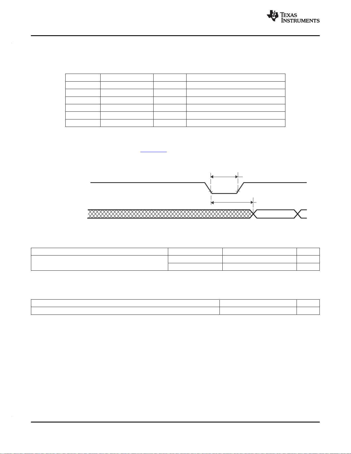
ADVANCEINFORMATION
XINT1, XINT2, XINT3
t
w(INT)
Interrupt Vector
t
d(INT)
Address bus
(internal)
TMS320F28069, TMS320F28068, TMS320F28067, TMS320F28066
TMS320F28065, TMS320F28064, TMS320F28063, TMS320F28062
SPRS698A–NOVEMBER 2010–REVISED JANUARY 2011
6.8.1 External Interrupts
Table 6-13. External Interrupt Registers
NAME ADDRESS SIZE (x16) DESCRIPTION
XINT1CR 0x00 7070 1 XINT1 configuration register
XINT2CR 0x00 7071 1 XINT2 configuration register
XINT3CR 0x00 7072 1 XINT3 configuration register
XINT1CTR 0x00 7078 1 XINT1 counter register
XINT2CTR 0x00 7079 1 XINT2 counter register
XINT3CTR 0x00 707A 1 XINT3 counter register
Each external interrupt can be enabled/disabled or qualified using positive, negative, or both positive and
negative edge. For more information, see the TMS320x2806x Piccolo System Control and Interrupts
Reference Guide (literature number SPRUH15).
6.8.1.1 External Interrupt Electrical Data/Timing
www.ti.com
Figure 6-10. External Interrupt Timing
Table 6-14. External Interrupt Timing Requirements
TEST CONDITIONS MIN MAX UNIT
(2)
t
w(INT)
(1) For an explanation of the input qualifier parameters, see Table 6-67.
(2) This timing is applicable to any GPIO pin configured for ADCSOC functionality.
Pulse duration, INT input low/high Synchronous 1t
With qualifier 1t
Table 6-15. External Interrupt Switching Characteristics
PARAMETER MIN MAX UNIT
t
d(INT)
(1) For an explanation of the input qualifier parameters, see Table 6-67.
Delay time, INT low/high to interrupt-vector fetch t
c(SCO)
(1)
+ t
(1)
c(SCO)
w(IQSW)
w(IQSW)
+ 12t
c(SCO)
cycles
cycles
cycles
74 Peripheral and Electrical Specifications Copyright © 2010–2011, Texas Instruments Incorporated
Submit Documentation Feedback
Product Folder Link(s): TMS320F28069 TMS320F28068 TMS320F28067 TMS320F28066 TMS320F28065
TMS320F28064 TMS320F28063 TMS320F28062
Page 75

ADVANCEINFORMATION
TMS320F28069, TMS320F28068, TMS320F28067, TMS320F28066
TMS320F28065, TMS320F28064, TMS320F28063, TMS320F28062
www.ti.com
6.9 Control Law Accelerator (CLA) Overview
The control law accelerator extends the capabilities of the C28x CPU by adding parallel processing.
Time-critical control loops serviced by the CLA can achieve low ADC sample to output delay. Thus, the
CLA enables faster system response and higher frequency control loops. Utilizing the CLA for time-critical
tasks frees up the main CPU to perform other system and communication functions concurently. The
following is a list of major features of the CLA.
• Clocked at the same rate as the main CPU (SYSCLKOUT).
• An independent architecture allowing CLA algorithm execution independent of the main C28x CPU.
– Complete bus architecture:
• Program address bus and program data bus
• Data address bus, data read bus, and data write bus
– Independent eight-stage pipeline.
– 12-bit program counter (MPC)
– Four 32-bit result registers (MR0–MR3)
– Two 16-bit auxillary registers (MAR0, MAR1)
– Status register (MSTF)
• Instruction set includes:
– IEEE single-precision (32-bit) floating-point math operations
– Floating-point math with parallel load or store
– Floating-point multiply with parallel add or subtract
– 1/X and 1/sqrt(X) estimations
– Data type conversions.
– Conditional branch and call
– Data load/store operations
• The CLA program code can consist of up to eight tasks or interrupt service routines.
– The start address of each task is specified by the MVECT registers.
– No limit on task size as long as the tasks fit within the CLA program memory space.
– One task is serviced at a time through to completion. There is no nesting of tasks.
– Upon task completion, a task-specific interrupt is flagged within the PIE.
– When a task finishes, the next highest-priority pending task is automatically started.
• Task trigger mechanisms:
– C28x CPU via the IACK instruction
– Task1 to Task7: the corresponding ADC, ePWM, eQEP, or eCAP module interrupt. For example:
• Task1: ADCINT1 or EPWM1_INT
• Task2: ADCINT2 or EPWM2_INT
• Task4: ADCINT4 or EPWM4_INT or EQEPx_INT or ECAPx_INT
• Task7: ADCINT7 or EPWM7_INT or EQEPx_INT or ECAPx_INT
– Task8: ADCINT8 or by CPU Timer 0 or EQEPx_INT or ECAPx_INT.
• Memory and Shared Peripherals:
– Two dedicated message RAMs for communication between the CLA and the main CPU.
– The C28x CPU can map CLA program and data memory to the main CPU space or CLA space.
– The CLA has direct access to the ADC Result registers, comparator registers, and the eCAP,
eQEP, and ePWM+HRPWM registers.
SPRS698A–NOVEMBER 2010–REVISED JANUARY 2011
Copyright © 2010–2011, Texas Instruments Incorporated Peripheral and Electrical Specifications 75
Submit Documentation Feedback
Product Folder Link(s): TMS320F28069 TMS320F28068 TMS320F28067 TMS320F28066 TMS320F28065
TMS320F28064 TMS320F28063 TMS320F28062
Page 76

ADVANCEINFORMATION
CLA_INT1 to CLA_INT8
MVECT1
MVECT2
MPERINT1
to
MPERINT8
PIE
Main
28x
CPU
CLA
Program
Memory
MMEMCFG
MCTL
MIFR
MIER
MIFRC
MIRUN
MIOVF
MICLR
MICLROVF
MPISRCSEL1
MVECT3
MVECT4
MVECT5
MVECT6
MVECT7
MVECT8
ain CP U B US
INT11
INT12
Peripheral Interrupts
ADCINT1 to ADCINT8
ECAP1_INT to ECAP3_INT
EQEP1_INT and EQEP2_INT
EPWM1_INT to EPWM8_INT
CPU Timer 0
Map to CLA or
CPU Space
CLA
Data
Memory
Comparator
Registers
eCAP
Registers
eQEP
Registers
ePWM
and
HRPWM
Registers
ADC
Result
Registers
CLA
Shared
Message
RAMs
Main CPU Read/Write Data Bus
CLA Program Address Bus
CLA Program Data Bus
Map to CLA or
CPU Space
CLA Data Bus
Main CPU Bus
MR0(32)
MPC(12)
MR1(32)
MR3(32)
MAR0(32)
MSTF(32)
MR2(32)
MAR1(32)
CLA Data Read Address Bus
CLA Data Write Data Bus
CLA Data Write Address Bus
CLA Data Read Data Bus
MEALLOW
Main CPU Read Data Bus
CLA Execution
Registers
CLA Control
Registers
SYSCLKOUT
CLAENCLK
SYSRS
LVF
LUF
IACK
TMS320F28069, TMS320F28068, TMS320F28067, TMS320F28066
TMS320F28065, TMS320F28064, TMS320F28063, TMS320F28062
SPRS698A–NOVEMBER 2010–REVISED JANUARY 2011
www.ti.com
Figure 6-11. CLA Block Diagram
76 Peripheral and Electrical Specifications Copyright © 2010–2011, Texas Instruments Incorporated
Submit Documentation Feedback
Product Folder Link(s): TMS320F28069 TMS320F28068 TMS320F28067 TMS320F28066 TMS320F28065
TMS320F28064 TMS320F28063 TMS320F28062
Page 77
ADVANCEINFORMATION
www.ti.com
TMS320F28069, TMS320F28068, TMS320F28067, TMS320F28066
TMS320F28065, TMS320F28064, TMS320F28063, TMS320F28062
SPRS698A–NOVEMBER 2010–REVISED JANUARY 2011
Table 6-16. CLA Control Registers
REGISTER NAME SIZE (x16) DESCRIPTION
MVECT1 0x1400 1 Yes CLA Interrupt/Task 1 Start Address
MVECT2 0x1401 1 Yes CLA Interrupt/Task 2 Start Address
MVECT3 0x1402 1 Yes CLA Interrupt/Task 3 Start Address
MVECT4 0x1403 1 Yes CLA Interrupt/Task 4 Start Address
MVECT5 0x1404 1 Yes CLA Interrupt/Task 5 Start Address
MVECT6 0x1405 1 Yes CLA Interrupt/Task 6 Start Address
MVECT7 0x1406 1 Yes CLA Interrupt/Task 7 Start Address
MVECT8 0x1407 1 Yes CLA Interrupt/Task 8 Start Address
MCTL 0x1410 1 Yes CLA Control Register
MMEMCFG 0x1411 1 Yes CLA Memory Configure Register
MPISRCSEL1 0x1414 2 Yes Peripheral Interrupt Source Select Register 1
MIFR 0x1420 1 Yes Interrupt Flag Register
MIOVF 0x1421 1 Yes Interrupt Overflow Register
MIFRC 0x1422 1 Yes Interrupt Force Register
MICLR 0x1423 1 Yes Interrupt Clear Register
MICLROVF 0x1424 1 Yes Interrupt Overflow Clear Register
MIER 0x1425 1 Yes Interrupt Enable Register
MIRUN 0x1426 1 Yes Interrupt RUN Register
MIPCTL 0x1427 1 Yes Interrupt Priority Control Register
(2)
MPC
(2)
MAR0
(2)
MAR1
(2)
MSTF
(2)
MR0
(2)
MR1
(2)
MR2
(2)
MR3
(1) All registers in this table are CSM protected
(2) The main C28x CPU has read only access to this register for debug purposes. The main CPU cannot perform CPU or debugger writes
to this register.
CLA1 EALLOW
ADDRESS PROTECTED
0x1428 1 – CLA Program Counter
0x142A 1 – CLA Aux Register 0
0x142B 1 – CLA Aux Register 1
0x142E 2 – CLA STF Register
0x1430 2 – CLA R0H Register
0x1434 2 – CLA R1H Register
0x1438 2 – CLA R2H Register
0x143C 2 – CLA R3H Register
(1)
Table 6-17. CLA Message RAM
ADDRESS RANGE SIZE (x16) DESCRIPTION
0x1480 – 0x14FF 128 CLA to CPU Message RAM
0x1500 – 0x157F 128 CPU to CLA Message RAM
Copyright © 2010–2011, Texas Instruments Incorporated Peripheral and Electrical Specifications 77
Submit Documentation Feedback
Product Folder Link(s): TMS320F28069 TMS320F28068 TMS320F28067 TMS320F28066 TMS320F28065
TMS320F28064 TMS320F28063 TMS320F28062
Page 78

ADVANCEINFORMATION
100-Pin
80-Pin
VDDA
VDDA
VREFLO
Tied To
VSSA
VSSA
VREFLO
VREFHI
A0
VREFHI
Tied To
A0
A1
A2
A1
A2
A3
A4
A4
A5
A6
A6
A7
B0
B0
B1
B1
B2
B2
B3
B4
B4
B5
B6
B6
B7
(3.3 V) VDDA
(Agnd) VSSA
VREFLO
Diff
Interface Reference
Comp1
VREFHI
A0
B0
AIO2
AIO10
A1
B1
10-Bit
DAC
A2
B2
COMP1OUT
A3
B3
AIO4
AIO12
A4
B4
Comp2
10-Bit
DAC
COMP2OUT
Comp3
10-Bit
DAC
COMP3OUT
ADC
B5
A5
AIO6
AIO14
A6
B6
A7
B7
Simultaneous Sampling Channels
Signal Pinout
Temperature Sensor
A5
B5
TMS320F28069, TMS320F28068, TMS320F28067, TMS320F28066
TMS320F28065, TMS320F28064, TMS320F28063, TMS320F28062
SPRS698A–NOVEMBER 2010–REVISED JANUARY 2011
6.10 Analog Block
A 12-bit ADC core is implemented that has different timings than the 12-bit ADC used on F280x/F2833x.
The ADC wrapper is modified to incorporate the new timings and also other enhancements to improve the
timing control of start of conversions. Figure 6-12 shows the interaction of the analog module with the rest
of the F2806x system.
www.ti.com
Figure 6-12. Analog Pin Configurations
78 Peripheral and Electrical Specifications Copyright © 2010–2011, Texas Instruments Incorporated
Product Folder Link(s): TMS320F28069 TMS320F28068 TMS320F28067 TMS320F28066 TMS320F28065
Submit Documentation Feedback
TMS320F28064 TMS320F28063 TMS320F28062
Page 79

ADVANCEINFORMATION
0,ValueDigital =
V0inputwhen £
3.3
V
VoltageAnalogInput
4096ValueDigital
REFLO
-
´=
V3.3inputV0when <<
4095,ValueDigital =
V3.3inputwhen ³
0,ValueDigital =
V0inputwhen £
VV
V
VoltageAnalogInput
4096ValueDigital
REFLOREFHI
REFLO
-
-
´=
V
inputV0when
REFHI
<<
4095,ValueDigital =
V
inputwhen
REFHI
³
TMS320F28069, TMS320F28068, TMS320F28067, TMS320F28066
TMS320F28065, TMS320F28064, TMS320F28063, TMS320F28062
www.ti.com
6.10.1 Analog-to-Digital Converter (ADC)
6.10.1.1 Features
The core of the ADC contains a single 12-bit converter fed by two sample-and-hold circuits. The
sample-and-hold circuits can be sampled simultaneously or sequentially. These, in turn, are fed by a total
of up to 16 analog input channels. The converter can be configured to run with an internal bandgap
reference to create true-voltage based conversions or with a pair of external voltage references
(V
REFHI/VREFLO
Contrary to previous ADC types, this ADC is not sequencer-based. It is easy for the user to create a
series of conversions from a single trigger. However, the basic principle of operation is centered around
the configurations of individual conversions, called SOCs, or Start-Of-Conversions.
Functions of the ADC module include:
• 12-bit ADC core with built-in dual sample-and-hold (S/H)
• Simultaneous sampling or sequential sampling modes
• Full range analog input: 0 V to 3.3 V fixed, or V
analog voltage is derived by:
– Internal Reference (V
external reference modes.)
) to create ratiometric-based conversions.
= V
REFLO
SSA
. V
REFHI/VREFLO
must not exceed V
REFHI
SPRS698A–NOVEMBER 2010–REVISED JANUARY 2011
ratiometric. The digital value of the input
when using either internal or
DDA
– External Reference (V
REFHI/VREFLO
connected to external references. V
REFHI
when using either internal or external reference modes.)
• Runs at full system clock, no prescaling required
• Up to 16-channel, multiplexed inputs
• 16 SOCs, configurable for trigger, sample window, and channel
• 16 result registers (individually addressable) to store conversion values
• Multiple trigger sources
– S/W – software immediate start
– ePWM 1–8
– GPIO XINT2
– CPU Timers 0/1/2
– ADCINT1/2
• 9 flexible PIE interrupts, can configure interrupt request after any conversion
must not exceed V
DDA
Copyright © 2010–2011, Texas Instruments Incorporated Peripheral and Electrical Specifications 79
Submit Documentation Feedback
Product Folder Link(s): TMS320F28069 TMS320F28068 TMS320F28067 TMS320F28066 TMS320F28065
TMS320F28064 TMS320F28063 TMS320F28062
Page 80

ADVANCEINFORMATION
TMS320F28069, TMS320F28068, TMS320F28067, TMS320F28066
TMS320F28065, TMS320F28064, TMS320F28063, TMS320F28062
SPRS698A–NOVEMBER 2010–REVISED JANUARY 2011
Table 6-18. ADC Configuration and Control Registers
www.ti.com
REGISTER NAME ADDRESS DESCRIPTION
ADCCTL1 0x7100 1 Yes Control 1 Register
ADCINTFLG 0x7104 1 No Interrupt Flag Register
ADCINTFLGCLR 0x7105 1 No Interrupt Flag Clear Register
ADCINTOVF 0x7106 1 No Interrupt Overflow Register
ADCINTOVFCLR 0x7107 1 No Interrupt Overflow Clear Register
ADCINTSEL1AND2 0x7108 1 Yes Interrupt 1 and 2 Selection Register
ADCINTSEL3AND4 0x7109 1 Yes Interrupt 3 and 4 Selection Register
ADCINTSEL5AND6 0x710A 1 Yes Interrupt 5 and 6 Selection Register
ADCINTSEL7AND8 0x710B 1 Yes Interrupt 7 and 8 Selection Register
ADCINTSEL9AND10 0x710C 1 Yes Interrupt 9 Selection Register (reserved Interrupt 10 Selection)
ADCSOCPRIORITYCTL 0x7110 1 Yes SOC Priority Control Register
ADCSAMPLEMODE 0x7112 1 Yes Sampling Mode Register
ADCINTSOCSEL1 0x7114 1 Yes Interrupt SOC Selection 1 Register (for 8 channels)
ADCINTSOCSEL2 0x7115 1 Yes Interrupt SOC Selection 2 Register (for 8 channels)
ADCSOCFLG1 0x7118 1 No SOC Flag 1 Register (for 16 channels)
ADCSOCFRC1 0x711A 1 No SOC Force 1 Register (for 16 channels)
ADCSOCOVF1 0x711C 1 No SOC Overflow 1 Register (for 16 channels)
ADCSOCOVFCLR1 0x711E 1 No SOC Overflow Clear 1 Register (for 16 channels)
ADCSOC0CTL to 0x7120 – 1 Yes SOC0 Control Register to SOC15 Control Register
ADCSOC15CTL 0x712F
ADCREFTRIM 0x7140 1 Yes Reference Trim Register
ADCOFFTRIM 0x7141 1 Yes Offset Trim Register
ADCREV 0x714F 1 No Revision Register
SIZE EALLOW
(x16) PROTECTED
Table 6-19. ADC Result Registers (Mapped to PF0)
REGISTER NAME ADDRESS DESCRIPTION
ADCRESULT0 to 0xB00 – 1 No ADC Result 0 Register to ADC Result 15 Register
ADCRESULT15 0xB0F
SIZE EALLOW
(x16) PROTECTED
80 Peripheral and Electrical Specifications Copyright © 2010–2011, Texas Instruments Incorporated
Submit Documentation Feedback
Product Folder Link(s): TMS320F28069 TMS320F28068 TMS320F28067 TMS320F28066 TMS320F28065
TMS320F28064 TMS320F28063 TMS320F28062
Page 81

ADVANCEINFORMATION
PF0 (CPU)
PF2 (CPU)
SYSCLKOUT
ADCENCLK
AIO
MUX
ADC
Channels
ADC
Core
12-Bit
0-Wait
Result
Registers
ADCINT 1
ADCINT 9
ADCTRIG 1
TINT 0
PIE
CPUTIMER 0
ADCTRIG 2
TINT 1
CPUTIMER 1
ADCTRIG 3
TINT 2
CPUTIMER 2
ADCTRIG 4
XINT 2SOC
XINT 2
ADCTRIG 5
SOCA 1
EPWM 1
ADCTRIG 6
SOCB 1
ADCTRIG 7
SOCA 2
EPWM 2
ADCTRIG 8
SOCB 2
ADCTRIG 9
SOCA 3
EPWM 3
ADCTRIG 10
SOCB 3
ADCTRIG 11
SOCA 4
EPWM 4
ADCTRIG 12
SOCB 4
ADCTRIG 13
SOCA 5
EPWM 5
ADCTRIG 14
SOCB 5
ADCTRIG 15
SOCA 6
EPWM 6
ADCTRIG 16
SOCB 6
ADCTRIG 17
SOCA 7
EPWM 7
ADCTRIG 18
SOCB 7
ADCTRIG 19
SOCA 8
EPWM 8
ADCTRIG 20
SOCB 8
www.ti.com
TMS320F28069, TMS320F28068, TMS320F28067, TMS320F28066
TMS320F28065, TMS320F28064, TMS320F28063, TMS320F28062
SPRS698A–NOVEMBER 2010–REVISED JANUARY 2011
Figure 6-13. ADC Connections
ADC Connections if the ADC is Not Used
It is recommended that the connections for the analog power pins be kept, even if the ADC is not used.
Following is a summary of how the ADC pins should be connected, if the ADC is not used in an
application:
• V
• V
• V
• ADCINAn, ADCINBn, V
When the ADC module is used in an application, unused ADC input pins should be connected to analog
ground (V
NOTE: Unused ADCIN pins that are multiplexed with AIO function should not be directly connected to
analog ground. They should be grounded through a 1-kΩ resistor. This is to prevent an errant code from
configuring these pins as AIO outputs and driving grounded pins to a logic-high state.
When the ADC is not used, be sure that the clock to the ADC module is not turned on to realize power
savings.
Copyright © 2010–2011, Texas Instruments Incorporated Peripheral and Electrical Specifications 81
– Connect to V
DDA
SSA
REFLO
– Connect to V
– Connect to V
).
SSA
Product Folder Link(s): TMS320F28069 TMS320F28068 TMS320F28067 TMS320F28066 TMS320F28065
DDIO
SS
SS
REFHI
TMS320F28064 TMS320F28063 TMS320F28062
– Connect to V
Submit Documentation Feedback
SSA
Page 82

ADVANCEINFORMATION
ADCSOCAO
ADCSOCBO
or
t
w(ADCSOCL)
TMS320F28069, TMS320F28068, TMS320F28067, TMS320F28066
TMS320F28065, TMS320F28064, TMS320F28063, TMS320F28062
SPRS698A–NOVEMBER 2010–REVISED JANUARY 2011
6.10.1.2 ADC Start-of-Conversion Electrical Data/Timing Table 6-20. External ADC Start-of-Conversion Switching Characteristics
PARAMETER MIN MAX UNIT
t
w(ADCSOCL)
Pulse duration, ADCSOCxO low 32t
c(HCO )
Figure 6-14. ADCSOCAO or ADCSOCBO Timing
6.10.1.3 On-Chip Analog-to-Digital Converter (ADC) Electrical Data/Timing
Table 6-21. ADC Electrical Characteristics
PARAMETER MIN TYP MAX UNIT
DC SPECIFICATIONS
Resolution 12 Bits
ADC clock 80-MHz device 0.001 40 MHz
Sample Window 7 64 ADC
ACCURACY
INL (Integral nonlinearity)
DNL (Differential nonlinearity) ±1 LSB
Offset error
(2)
Overall gain error with internal reference 10 LSB
Overall gain error with external reference 10 LSB
Channel-to-channel offset variation ±4 LSB
Channel-to-channel gain variation ±4 LSB
ADC temperature coefficient with internal reference –50 ppm/°C
ADC temperature coefficient with external reference –20 ppm/°C
ANALOG INPUT
Analog input voltage with internal reference 0 3.3 V
Analog input voltage with external reference V
V
input voltage
REFLO
V
input voltage
REFHI
Input capacitance 5 pF
Input leakage current ±2 mA
(1) INL will degrade when the ADC input voltage goes above V
(2) 1 LSB has the weighted value of full-scale range (FSR)/4096. FSR is 3.3 V with internal reference and V
reference.
(3) Periodic self-recalibration will remove system-level and temperature dependencies on the ADC zero offset error.
(4) V
(5) V
is always connected to V
REFLO
must not exceed V
REFHI
PN/PFP device, the input signal on ADCINA0 must not exceed V
(1)
40-MHz clock (3 MSPS) ±2 LSB
Executing Device_Cal 10 LSB
function
Executing periodic 10
self-recalibration
(4)
(5)
with V
REFLO
.
DDA
on the 80-pin PN/PFP device.
SSA
when using either internal or external reference modes. Since V
DDA
DDA
(3)
REFLO
V
SSA
2.64 V
= V
SSA
.
1.98 V
- V
REFHI
is tied to ADCINA0 on the 80-pin
REFHI
REFLO
V
REFHI
0.66 V
DDA
DDA
for external
www.ti.com
cycles
Clocks
V
V
82 Peripheral and Electrical Specifications Copyright © 2010–2011, Texas Instruments Incorporated
Submit Documentation Feedback
Product Folder Link(s): TMS320F28069 TMS320F28068 TMS320F28067 TMS320F28066 TMS320F28065
TMS320F28064 TMS320F28063 TMS320F28062
Page 83

ADVANCEINFORMATION
ADCPWDN/
ADCBGPWD/
ADCREFPWD/
ADCENABLE
Request for ADC
Conversion
t
d(PWD)
www.ti.com
TMS320F28069, TMS320F28068, TMS320F28067, TMS320F28066
TMS320F28065, TMS320F28064, TMS320F28063, TMS320F28062
SPRS698A–NOVEMBER 2010–REVISED JANUARY 2011
Table 6-22. ADC Power Modes
ADC OPERATING MODE CONDITIONS I
Mode A – Operating Mode ADC Clock Enabled 13 mA
Bandgap On (ADCBGPWD = 1)
Reference On (ADCREFPWD = 1)
ADC Powered Up (ADCPWRDN = 1)
Mode B – Quick Wake Mode ADC Clock Enabled 4 mA
Bandgap On (ADCBGPWD = 1)
Reference On (ADCREFPWD = 1)
ADC Powered Up (ADCPWRDN = 0)
Mode C – Comparator-Only Mode ADC Clock Enabled 1.5 mA
Bandgap On (ADCBGPWD = 1)
Reference On (ADCREFPWD = 0)
ADC Powered Up (ADCPWRDN = 0)
Mode D – Off Mode ADC Clock Enabled 0.075 mA
Bandgap On (ADCBGPWD = 0)
Reference On (ADCREFPWD = 0)
ADC Powered Up (ADCPWRDN = 0)
DDA
UNITS
6.10.1.3.1 Internal Temperature Sensor
Table 6-23. Temperature Sensor Coefficient
PARAMETER
T
SLOPE
T
OFFSET
(1) The temperature sensor slope and offset are given in terms of ADC LSBs using the internal reference of the ADC. Values must be
adjusted accordingly in external reference mode to the external reference voltage.
(2) ADC temperature coeffieicient is accounted for in this specification
(3) Output of the temperature sensor (in terms of LSBs) is sign-consistent with the direction of the temperature movement. Increasing
temperatures will give increasing ADC values relative to an initial value; decreasing temperatures will give decreasing ADC values
relative to an initial value.
Degrees C of temperature movement per measured ADC LSB change 0.18
of the temperature sensor
ADC output at 0°C of the temperature sensor 1750 LSB
(1)
MIN TYP MAX UNIT
(2)(3)
°C/LSB
6.10.1.3.2 ADC Power-Up Control Bit Timing
Table 6-24. ADC Power-Up Delays
PARAMETER
t
d(PWD)
(1) Timings maintain compatibility to the ADC module. The 2806x ADC supports driving all 3 bits at the same time t
conversion.
Delay time for the ADC to be stable after power up 1 ms
(1)
MIN TYP MAX UNIT
Figure 6-15. ADC Conversion Timing
d(PWD)
ms before first
Copyright © 2010–2011, Texas Instruments Incorporated Peripheral and Electrical Specifications 83
Product Folder Link(s): TMS320F28069 TMS320F28068 TMS320F28067 TMS320F28066 TMS320F28065
TMS320F28064 TMS320F28063 TMS320F28062
Submit Documentation Feedback
Page 84

ADVANCEINFORMATION
ac
R
s
ADCIN
C
5 pF
p
C
1.6 pF
h
Switch
Typical Values of the Input Circuit Components:
Switch Resistance (R ): 3.4 k
on
W
Sampling Capacitor (C ): 1.6 pF
h
Parasitic Capacitance (C ): 5 pF
p
Source Resistance (R ): 50
s
W
28x DSP
Source
Signal
3.4 k
W
R
on
TMS320F28069, TMS320F28068, TMS320F28067, TMS320F28066
TMS320F28065, TMS320F28064, TMS320F28063, TMS320F28062
SPRS698A–NOVEMBER 2010–REVISED JANUARY 2011
Figure 6-16. ADC Input Impedance Model
www.ti.com
84 Peripheral and Electrical Specifications Copyright © 2010–2011, Texas Instruments Incorporated
Product Folder Link(s): TMS320F28069 TMS320F28068 TMS320F28067 TMS320F28066 TMS320F28065
Submit Documentation Feedback
TMS320F28064 TMS320F28063 TMS320F28062
Page 85

ADVANCEINFORMATION
SOC0
ADCCLK
ADCRESULT 0
S/H Window Pulse to Core
ADCCTL 1.INTPULSEPOS
ADCSOCFLG 1.SOC 0
ADCINTFLG.ADCINTx
SOC1 SOC 2
9 15 22 24 3720
Result 0 Latched
ADCSOCFLG 1.SOC 1
ADCSOCFLG 1.SOC 2
ADCRESULT 1
EOC0 Pulse
EOC1 Pulse
Conversion 0
13 ADC Clocks
Minimum
7 ADCCLKs
6
ADCCLKs
Conversion 1
13 ADC Clocks
Minimum
7 ADCCLKs
2 ADCCLKs
1 ADCCLK
Analog Input
SOC1 Sample
Window
SOC0 Sample
Window
SOC2 Sample
Window
TMS320F28069, TMS320F28068, TMS320F28067, TMS320F28066
TMS320F28065, TMS320F28064, TMS320F28063, TMS320F28062
www.ti.com
6.10.1.3.3 ADC Sequential and Simultaneous Timings
SPRS698A–NOVEMBER 2010–REVISED JANUARY 2011
Figure 6-17. Timing Example for Sequential Mode / Late Interrupt Pulse
Copyright © 2010–2011, Texas Instruments Incorporated Peripheral and Electrical Specifications 85
Product Folder Link(s): TMS320F28069 TMS320F28068 TMS320F28067 TMS320F28066 TMS320F28065
Submit Documentation Feedback
TMS320F28064 TMS320F28063 TMS320F28062
Page 86

ADVANCEINFORMATION
Conversion 0
13 ADC Clocks
Minimum
7 ADCCLKs
SOC0
ADCCLK
ADCRESULT 0
S/H Window Pulse to Core
ADCCTL1.INTPULSEPOS
ADCSOCFLG 1.SOC 0
ADCINTFLG.ADCINTx
SOC1 SOC2
9 15 22 24 37
6
ADCCLKs
20
Result 0 Latched
Conversion 1
13 ADC Clocks
Minimum
7 ADCCLKs
ADCSOCFLG 1.SOC 1
ADCSOCFLG 1.SOC 2
ADCRESULT 1
EOC0 Pulse
EOC1 Pulse
EOC2 Pulse
2 ADCCLKs
Analog Input
SOC1 Sample
Window
SOC0 Sample
Window
SOC2 Sample
Window
TMS320F28069, TMS320F28068, TMS320F28067, TMS320F28066
TMS320F28065, TMS320F28064, TMS320F28063, TMS320F28062
SPRS698A–NOVEMBER 2010–REVISED JANUARY 2011
www.ti.com
Figure 6-18. Timing Example for Sequential Mode / Early Interrupt Pulse
86 Peripheral and Electrical Specifications Copyright © 2010–2011, Texas Instruments Incorporated
Product Folder Link(s): TMS320F28069 TMS320F28068 TMS320F28067 TMS320F28066 TMS320F28065
Submit Documentation Feedback
TMS320F28064 TMS320F28063 TMS320F28062
Page 87

ADVANCEINFORMATION
Conversion 0 (A)
13 ADC Clocks
Minimum
7 ADCCLKs
SOC0 (A/B)
ADCCLK
ADCRESULT 0
S/H Window Pulse to Core
ADCCTL1 .INTPULSEPOS
ADCSOCFLG 1.SOC0
ADCINTFLG .ADCINTx
SOC2 (A/B)
9 22 24 37
19
ADCCLKs
20
Result 0 (A) Latched
Conversion 0 (B)
13 ADC Clocks
Minimum
7 ADCCLKs
ADCSOCFLG 1.SOC1
ADCSOCFLG 1.SOC2
ADCRESULT 1
Result 0 (B) Latched
Conversion 1 (A)
13 ADC Clocks
ADCRESULT 2
50
EOC0 Pulse
EOC1 Pulse
EOC2 Pulse
1 ADCCLK
2 ADCCLKs
2 ADCCLKs
Analog Input B
SOC0 Sample
B Window
SOC2 Sample
B Window
Analog Input A
SOC0 Sample
A Window
SOC2 Sample
A Window
www.ti.com
TMS320F28069, TMS320F28068, TMS320F28067, TMS320F28066
TMS320F28065, TMS320F28064, TMS320F28063, TMS320F28062
SPRS698A–NOVEMBER 2010–REVISED JANUARY 2011
Figure 6-19. Timing Example for Simultaneous Mode / Late Interrupt Pulse
Copyright © 2010–2011, Texas Instruments Incorporated Peripheral and Electrical Specifications 87
Product Folder Link(s): TMS320F28069 TMS320F28068 TMS320F28067 TMS320F28066 TMS320F28065
TMS320F28064 TMS320F28063 TMS320F28062
Submit Documentation Feedback
Page 88

ADVANCEINFORMATION
Conversion 0 (A)
13 ADC Clocks
Minimum
7 ADCCLKs
SOC0 (A/B)
ADCCLK
ADCRESULT 0
S/H Window Pulse to Core
ADCCTL1 .INTPULSEPOS
ADCSOCFLG 1.SOC0
ADCINTFLG .ADCINTx
SOC2 (A/B)
9 22 24 37
19
ADCCLKs
20
Result 0 (A) Latched
Conversion 0 (B)
13 ADC Clocks
Minimum
7 ADCCLKs
ADCSOCFLG 1.SOC1
ADCSOCFLG 1.SOC2
ADCRESULT 1 Result 0 ( B) Latched
Conversion 1 (A)
13 ADC Clocks
ADCRESULT 2
50
EOC0 Pulse
EOC1 Pulse
EOC2 Pulse
2 ADCCLKs
2 ADCCLKs
Analog Input B
SOC0 Sample
B Window
SOC2 Sample
B Window
Analog Input A
SOC0 Sample
A Window
SOC2 Sample
A Window
TMS320F28069, TMS320F28068, TMS320F28067, TMS320F28066
TMS320F28065, TMS320F28064, TMS320F28063, TMS320F28062
SPRS698A–NOVEMBER 2010–REVISED JANUARY 2011
www.ti.com
Figure 6-20. Timing Example for Simultaneous Mode / Early Interrupt Pulse
88 Peripheral and Electrical Specifications Copyright © 2010–2011, Texas Instruments Incorporated
Product Folder Link(s): TMS320F28069 TMS320F28068 TMS320F28067 TMS320F28066 TMS320F28065
TMS320F28064 TMS320F28063 TMS320F28062
Submit Documentation Feedback
Page 89

ADVANCEINFORMATION
To COMPy A or B input
To ADC Channel X
1
0
AIOx Pin
AIOxIN
AIOxINE
SYNC
SYSCLK
Logic implemented in GPIO MUX block
AIODAT Reg
(Read)
AIODAT Reg
(Latch)
AIOSET,
AIOCLEAR,
AIOTOGGLE
Regs
AIOMUX 1 Reg
1
0
AIOxDIR
(1 = Input,
0 = Output)
(0 = Input, 1 = Output)
AIODIR Reg
(Latch)
0
www.ti.com
6.10.2 ADC MUX
TMS320F28069, TMS320F28068, TMS320F28067, TMS320F28066
TMS320F28065, TMS320F28064, TMS320F28063, TMS320F28062
SPRS698A–NOVEMBER 2010–REVISED JANUARY 2011
Figure 6-21. AIOx Pin Multiplexing
The ADC channel and Comparator functions are always available. The digital I/O function is available only
when the respective bit in the AIOMUX1 register is 0. In this mode, reading the AIODAT register reflects
the actual pin state.
The digital I/O function is disabled when the respective bit in the AIOMUX1 register is 1. In this mode,
reading the AIODAT register reflects the output latch of the AIODAT register and the input digital I/O buffer
is disabled to prevent analog signals from generating noise.
On reset, the digital function is disabled. If the pin is used as an analog input, users should keep the AIO
function disabled for that pin.
Copyright © 2010–2011, Texas Instruments Incorporated Peripheral and Electrical Specifications 89
Product Folder Link(s): TMS320F28069 TMS320F28068 TMS320F28067 TMS320F28066 TMS320F28065
Submit Documentation Feedback
TMS320F28064 TMS320F28063 TMS320F28062
Page 90
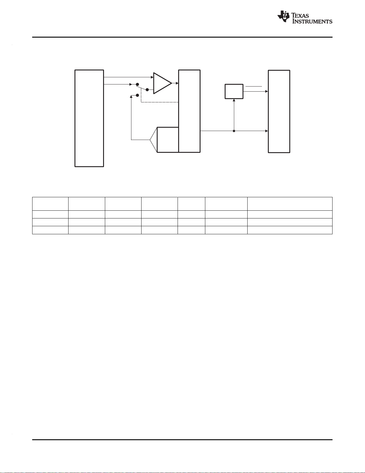
ADVANCEINFORMATION
AIO
MUX
COMP x A
COMP x B
COMP x
+
DAC x
Wrapper
DAC
Core
10-Bit
+
-
COMP
COMPxOUT
GPIO
MUX
TZ1/2/3
ePWM
TMS320F28069, TMS320F28068, TMS320F28067, TMS320F28066
TMS320F28065, TMS320F28064, TMS320F28063, TMS320F28062
SPRS698A–NOVEMBER 2010–REVISED JANUARY 2011
6.10.3 Comparator Block
Figure 6-22 shows the interaction of the Comparator modules with the rest of the system.
Figure 6-22. Comparator Block Diagram
Table 6-25. Comparator Control Registers
www.ti.com
REGISTER COMP1 COMP2 COMP3 SIZE EALLOW
NAME ADDRESS ADDRESS ADDRESS (x16) PROTECTED
COMPCTL 0x6400 0x6420 0x6440 1 Yes Comparator Control Register
COMPSTS 0x6402 0x6422 0x6442 1 No Comparator Status Register
DACVAL 0x6406 0x6426 0x6446 1 Yes DAC Value Register
DESCRIPTION
90 Peripheral and Electrical Specifications Copyright © 2010–2011, Texas Instruments Incorporated
Product Folder Link(s): TMS320F28069 TMS320F28068 TMS320F28067 TMS320F28066 TMS320F28065
TMS320F28064 TMS320F28063 TMS320F28062
Submit Documentation Feedback
Page 91

ADVANCEINFORMATION
Settling Time (ns)
0
100
200
300
400
500
600
700
800
900
1000
1100
0 50 100 150 200 250 300 350 400 450 500
DAC Step Size (Codes)
15 Codes 7 Codes 3 Codes 1 Code
DAC Accuracy
TMS320F28069, TMS320F28068, TMS320F28067, TMS320F28066
TMS320F28065, TMS320F28064, TMS320F28063, TMS320F28062
www.ti.com
6.10.3.1 On-Chip Comparator/DAC Electrical Data/Timing
Table 6-26. Electrical Characteristics of the Comparator/DAC
CHARACTERISTIC MIN TYP MAX UNITS
Comparator
Comparator Input Range V
Comparator response time to PWM Trip Zone (Async) 30 ns
Input Offset ±5 mV
Input Hysteresis
DAC Output Range V
DAC resolution 10 bits
DAC settling time See
DAC Gain –1.5 %
DAC Offset 10 mV
Monotonic Yes
INL ±3 LSB
(1) Hysteresis on the comparator inputs is achieved with a Schmidt trigger configuration. This results in an effective 100-kΩ feedback
resistance between the output of the comparator and the non-inverting input of the comparator.
(1)
DAC
SPRS698A–NOVEMBER 2010–REVISED JANUARY 2011
– V
SSA
DDA
35 mV
– V
SSA
DDA
Figure 6-23
V
V
Copyright © 2010–2011, Texas Instruments Incorporated Peripheral and Electrical Specifications 91
Product Folder Link(s): TMS320F28069 TMS320F28068 TMS320F28067 TMS320F28066 TMS320F28065
Figure 6-23. DAC Settling Time
Submit Documentation Feedback
TMS320F28064 TMS320F28063 TMS320F28062
Page 92

ADVANCEINFORMATION
6.02
1.76)(SINADN-
=
TMS320F28069, TMS320F28068, TMS320F28067, TMS320F28066
TMS320F28065, TMS320F28064, TMS320F28063, TMS320F28062
SPRS698A–NOVEMBER 2010–REVISED JANUARY 2011
6.11 Detailed Descriptions
Integral Nonlinearity
Integral nonlinearity refers to the deviation of each individual code from a line drawn from zero through full
scale. The point used as zero occurs one-half LSB before the first code transition. The full-scale point is
defined as level one-half LSB beyond the last code transition. The deviation is measured from the center
of each particular code to the true straight line between these two points.
Differential Nonlinearity
An ideal ADC exhibits code transitions that are exactly 1 LSB apart. DNL is the deviation from this ideal
value. A differential nonlinearity error of less than ±1 LSB ensures no missing codes.
Zero Offset
The major carry transition should occur when the analog input is at zero volts. Zero error is defined as the
deviation of the actual transition from that point.
Gain Error
The first code transition should occur at an analog value one-half LSB above negative full scale. The last
transition should occur at an analog value one and one-half LSB below the nominal full scale. Gain error is
the deviation of the actual difference between first and last code transitions and the ideal difference
between first and last code transitions.
www.ti.com
Signal-to-Noise Ratio + Distortion (SINAD)
SINAD is the ratio of the rms value of the measured input signal to the rms sum of all other spectral
components below the Nyquist frequency, including harmonics but excluding dc. The value for SINAD is
expressed in decibels.
Effective Number of Bits (ENOB)
For a sine wave, SINAD can be expressed in terms of the number of bits. Using the following
formula, it is possible to get a measure of performance expressed as N, the effective
number of bits. Thus, effective number of bits for a device for sine wave inputs at a given input frequency
can be calculated directly from its measured SINAD.
Total Harmonic Distortion (THD)
THD is the ratio of the rms sum of the first nine harmonic components to the rms value of the measured
input signal and is expressed as a percentage or in decibels.
Spurious Free Dynamic Range (SFDR)
SFDR is the difference in dB between the rms amplitude of the input signal and the peak spurious signal.
92 Peripheral and Electrical Specifications Copyright © 2010–2011, Texas Instruments Incorporated
Submit Documentation Feedback
Product Folder Link(s): TMS320F28069 TMS320F28068 TMS320F28067 TMS320F28066 TMS320F28065
TMS320F28064 TMS320F28063 TMS320F28062
Page 93

ADVANCEINFORMATION
1)(SPIBRR
LSPCLK
rateBaud
+
=
127to3SPIBRRwhen =
4
LSPCLK
rateBaud =
21,0,SPIBRRwhen =
TMS320F28069, TMS320F28068, TMS320F28067, TMS320F28066
TMS320F28065, TMS320F28064, TMS320F28063, TMS320F28062
www.ti.com
6.12 Serial Peripheral Interface (SPI) Module
The device includes the four-pin serial peripheral interface (SPI) module. Up to two SPI modules are
available. The SPI is a high-speed, synchronous serial I/O port that allows a serial bit stream of
programmed length (one to sixteen bits) to be shifted into and out of the device at a programmable
bit-transfer rate. Normally, the SPI is used for communications between the MCU and external peripherals
or another processor. Typical applications include external I/O or peripheral expansion through devices
such as shift registers, display drivers, and ADCs. Multidevice communications are supported by the
master/slave operation of the SPI.
The SPI module features include:
• Four external pins:
– SPISOMI: SPI slave-output/master-input pin
– SPISIMO: SPI slave-input/master-output pin
– SPISTE: SPI slave transmit-enable pin
– SPICLK: SPI serial-clock pin
NOTE: All four pins can be used as GPIO if the SPI module is not used.
• Two operational modes: master and slave
Baud rate: 125 different programmable rates.
SPRS698A–NOVEMBER 2010–REVISED JANUARY 2011
• Data word length: one to sixteen data bits
• Four clocking schemes (controlled by clock polarity and clock phase bits) include:
– Falling edge without phase delay: SPICLK active-high. SPI transmits data on the falling edge of the
SPICLK signal and receives data on the rising edge of the SPICLK signal.
– Falling edge with phase delay: SPICLK active-high. SPI transmits data one half-cycle ahead of the
falling edge of the SPICLK signal and receives data on the falling edge of the SPICLK signal.
– Rising edge without phase delay: SPICLK inactive-low. SPI transmits data on the rising edge of the
SPICLK signal and receives data on the falling edge of the SPICLK signal.
– Rising edge with phase delay: SPICLK inactive-low. SPI transmits data one half-cycle ahead of the
falling edge of the SPICLK signal and receives data on the rising edge of the SPICLK signal.
• Simultaneous receive and transmit operation (transmit function can be disabled in software)
• Transmitter and receiver operations are accomplished through either interrupt-driven or polled
algorithms.
• Nine SPI module control registers: Located in control register frame beginning at address 7040h.
NOTE
All registers in this module are 16-bit registers that are connected to Peripheral Frame 2.
When a register is accessed, the register data is in the lower byte (7–0), and the upper byte
(15–8) is read as zeros. Writing to the upper byte has no effect.
Enhanced feature:
• 4-level transmit/receive FIFO
• Delayed transmit control
• Bi-directional 3 wire SPI mode support
• Audio data receive support via SPISTE inversion
Copyright © 2010–2011, Texas Instruments Incorporated Peripheral and Electrical Specifications 93
Submit Documentation Feedback
Product Folder Link(s): TMS320F28069 TMS320F28068 TMS320F28067 TMS320F28066 TMS320F28065
TMS320F28064 TMS320F28063 TMS320F28062
Page 94
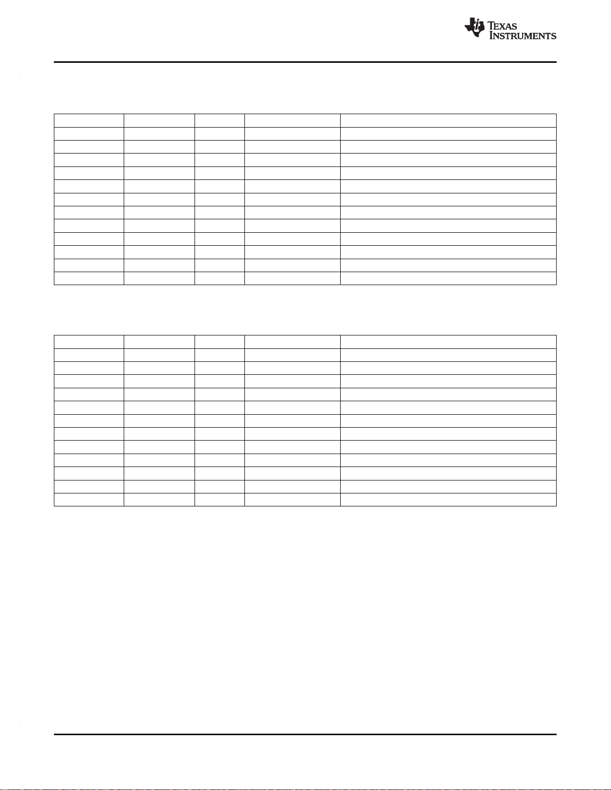
ADVANCEINFORMATION
TMS320F28069, TMS320F28068, TMS320F28067, TMS320F28066
TMS320F28065, TMS320F28064, TMS320F28063, TMS320F28062
SPRS698A–NOVEMBER 2010–REVISED JANUARY 2011
The SPI port operation is configured and controlled by the registers listed in Table 6-27 and Table 6-28.
Table 6-27. SPI-A Registers
NAME ADDRESS SIZE (x16) EALLOW PROTECTED DESCRIPTION
SPICCR 0x7040 1 No SPI-A Configuration Control Register
SPICTL 0x7041 1 No SPI-A Operation Control Register
SPISTS 0x7042 1 No SPI-A Status Register
SPIBRR 0x7044 1 No SPI-A Baud Rate Register
SPIRXEMU 0x7046 1 No SPI-A Receive Emulation Buffer Register
SPIRXBUF 0x7047 1 No SPI-A Serial Input Buffer Register
SPITXBUF 0x7048 1 No SPI-A Serial Output Buffer Register
SPIDAT 0x7049 1 No SPI-A Serial Data Register
SPIFFTX 0x704A 1 No SPI-A FIFO Transmit Register
SPIFFRX 0x704B 1 No SPI-A FIFO Receive Register
SPIFFCT 0x704C 1 No SPI-A FIFO Control Register
SPIPRI 0x704F 1 No SPI-A Priority Control Register
(1) Registers in this table are mapped to Peripheral Frame 2. This space only allows 16-bit accesses. 32-bit accesses produce undefined
results.
(1)
www.ti.com
Table 6-28. SPI-B Registers
NAME ADDRESS SIZE (x16) EALLOW PROTECTED DESCRIPTION
SPICCR 0x7740 1 No SPI-B Configuration Control Register
SPICTL 0x7741 1 No SPI-B Operation Control Register
SPISTS 0x7742 1 No SPI-B Status Register
SPIBRR 0x7744 1 No SPI-B Baud Rate Register
SPIRXEMU 0x7746 1 No SPI-B Receive Emulation Buffer Register
SPIRXBUF 0x7747 1 No SPI-B Serial Input Buffer Register
SPITXBUF 0x7748 1 No SPI-B Serial Output Buffer Register
SPIDAT 0x7749 1 No SPI-B Serial Data Register
SPIFFTX 0x774A 1 No SPI-B FIFO Transmit Register
SPIFFRX 0x774B 1 No SPI-B FIFO Receive Register
SPIFFCT 0x774C 1 No SPI-B FIFO Control Register
SPIPRI 0x774F 1 No SPI-B Priority Control Register
(1) Registers in this table are mapped to Peripheral Frame 2. This space only allows 16-bit accesses. 32-bit accesses produce undefined
results.
(1)
94 Peripheral and Electrical Specifications Copyright © 2010–2011, Texas Instruments Incorporated
Submit Documentation Feedback
Product Folder Link(s): TMS320F28069 TMS320F28068 TMS320F28067 TMS320F28066 TMS320F28065
TMS320F28064 TMS320F28063 TMS320F28062
Page 95
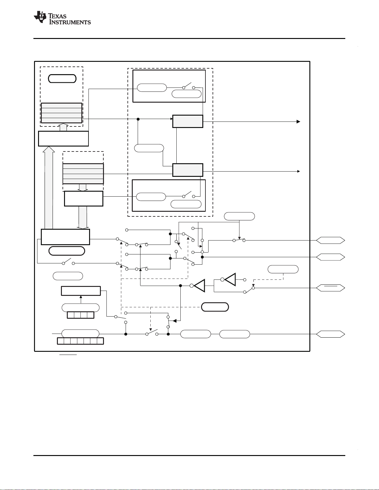
ADVANCEINFORMATION
S
SPICTL.0
SPI INT FLAG
SPI INT
ENA
SPISTS.6
S
Clock
Polarity
Talk
LSPCLK
SPI Bit Rate
State Control
Clock
Phase
Receiver
Overrun Flag
SPICTL.4
Overrun
INT ENA
SPICCR.3 - 0
SPIBRR.6 - 0
SPICCR.6
SPICTL.3
SPIDAT.15 - 0
SPICTL.1
M
S
M
Master/Slave
SPISTS.7
SPIDAT
Data Register
M
S
SPICTL.2
SPI Char
SPISIMO
SPISOMI
SPICLK
SW2
S
M
M
S
SW3
To CPU
M
SW1
RX FIFO _0
RX FIFO _1
-----
RX FIFO _3
TX FIFO Registers
TX FIFO _0
TX FIFO _1
-----
TX FIFO _3
RX FIFO Registers
16
16
16
TX Interrupt
Logic
RX Interrupt
Logic
SPIINT
SPITX
SPIFFOVF
FLAG
SPIFFRX.15
TX FIFO Interrupt
RX FIFO Interrupt
SPIRXBUF
SPITXBUF
SPIFFTX.14
SPIFFENA
SPISTE
16
0
12
3
0
12
3
4
5
6
TW
TW
TW
SPIPRI.0
TRIWIRE
SPIPRI.1
STEINV
STEINV
SPIRXBUF
Buffer Register
SPITXBUF
Buffer Register
www.ti.com
Figure 6-24 is a block diagram of the SPI in slave mode.
TMS320F28069, TMS320F28068, TMS320F28067, TMS320F28066
TMS320F28065, TMS320F28064, TMS320F28063, TMS320F28062
SPRS698A–NOVEMBER 2010–REVISED JANUARY 2011
Figure 6-24. SPI Module Block Diagram (Slave Mode)
A. SPISTE is driven low by the master for a slave device.
6.12.1 Serial Peripheral Interface (SPI) Master Mode Electrical Data/ Timing
Table 6-29 lists the master mode timing (clock phase = 0) and Table 6-30 lists the master mode timing
(clock phase = 1). Figure 6-25 and Figure 6-26 show the timing waveforms.
Copyright © 2010–2011, Texas Instruments Incorporated Peripheral and Electrical Specifications 95
Product Folder Link(s): TMS320F28069 TMS320F28068 TMS320F28067 TMS320F28066 TMS320F28065
TMS320F28064 TMS320F28063 TMS320F28062
Submit Documentation Feedback
Page 96

ADVANCEINFORMATION
TMS320F28069, TMS320F28068, TMS320F28067, TMS320F28066
TMS320F28065, TMS320F28064, TMS320F28063, TMS320F28062
SPRS698A–NOVEMBER 2010–REVISED JANUARY 2011
www.ti.com
Table 6-29. SPI Master Mode External Timing (Clock Phase = 0)
(1)(2)(3)(4)(5)
SPI WHEN (SPIBRR + 1) IS EVEN OR SPI WHEN (SPIBRR + 1) IS ODD
NO. UNIT
SPIBRR = 0 OR 2 AND SPIBRR > 3
MIN MAX MIN MAX
1 t
2 t
t
3 t
t
4 t
t
5 t
t
8 t
t
9 t
t
c(SPC)M
w(SPCH)M
w(SPCL)M
w(SPCL)M
w(SPCH)M
d(SPCH-SIMO)M
d(SPCL-SIMO)M
v(SPCL-SIMO)M
v(SPCH-SIMO)M
su(SOMI-SPCL)M
su(SOMI-SPCH)M
v(SPCL-SOMI)M
v(SPCH-SOMI)M
Cycle time, SPICLK 4t
Pulse duration, SPICLK high 0.5t
(clock polarity = 0)
Pulse duration, SPICLK low 0.5t
(clock polarity = 1)
Pulse duration, SPICLK low 0.5t
(clock polarity = 0)
Pulse duration, SPICLK high 0.5
(clock polarity = 1)
c(SPC)M
c(SPC)M
c(SPC)M
tc(SPC)M
c(LCO)
– 10 0.5t
– 10 0.5t
– 10 0.5
– 10 0.5t
128t
c(SPC)M
c(SPC)M
tc(SPC)M
c(SPC)M
c(LCO)
0.5t
0.5t
0.5t
0.5t
c(SPC)M
c(SPC)M
c(SPC)M
c(SPC)M
– 0.5t
– 0.5t
+ 0.5t
+ 0.5t
5t
c(LCO)
– 10 0.5t
c(LCO)
– 10 0.5t
c(LCO)
– 10 0.5t
c(LCO)
– 10 0.5t
c(LCO)
c(SPC)M
c(SPC)M
c(SPC)M
c(SPC)M
127t
– 0.5t
– 0.5t
+ 0.5t
+ 0.5t
c(LCO)
c(LCO)
c(LCO)
c(LCO)
c(LCO)
Delay time, SPICLK high to SPISIMO 10 10 ns
valid (clock polarity = 0)
Delay time, SPICLK low to SPISIMO 10 10
valid (clock polarity = 1)
Valid time, SPISIMO data valid after 0.5t
SPICLK low (clock polarity = 0)
Valid time, SPISIMO data valid after 0.5t
SPICLK high (clock polarity = 1)
– 10 0.5t
c(SPC)M
– 10 0.5t
c(SPC)M
c(SPC)M
c(SPC)M
+ 0.5t
+ 0.5t
– 10 ns
c(LCO)
– 10
c(LCO)
Setup time, SPISOMI before SPICLK 35 35 ns
low (clock polarity = 0)
Setup time, SPISOMI before SPICLK 35 35
high (clock polarity = 1)
Valid time, SPISOMI data valid after 0.25t
SPICLK low (clock polarity = 0)
Valid time, SPISOMI data valid after 0.25t
SPICLK high (clock polarity = 1)
– 10 0.5t
c(SPC)M
– 10 0.5t
c(SPC)M
c(SPC)M
c(SPC)M
– 0.5t
– 0.5t
– 10 ns
c(LCO)
– 10
c(LCO)
(1) The MASTER / SLAVE bit (SPICTL.2) is set and the CLOCK PHASE bit (SPICTL.3) is cleared.
(2) t
(3) t
(4) Internal clock prescalers must be adjusted such that the SPI clock speed is limited to the following SPI clock rate:
= SPI clock cycle time = LSPCLK/4 or LSPCLK/(SPIBRR +1)
c(SPC)
= LSPCLK cycle time
c(LCO)
Master mode transmit 15-MHz MAX, master mode receive 10-MHz MAX
Slave mode transmit 10-MHz MAX, slave mode receive 10-MHz MAX.
(5) The active edge of the SPICLK signal referenced is controlled by the clock polarity bit (SPICCR.6).
ns
ns
ns
96 Peripheral and Electrical Specifications Copyright © 2010–2011, Texas Instruments Incorporated
Submit Documentation Feedback
Product Folder Link(s): TMS320F28069 TMS320F28068 TMS320F28067 TMS320F28066 TMS320F28065
TMS320F28064 TMS320F28063 TMS320F28062
Page 97

ADVANCEINFORMATION
9
4
SPISOMI
SPISIMO
SPICLK
(clock polarity = 1)
SPICLK
(clock polarity = 0)
Master In Data
Must Be Valid
Master Out Data Is Valid
SPISTE
(A)
1
2
3
5
8
www.ti.com
TMS320F28069, TMS320F28068, TMS320F28067, TMS320F28066
TMS320F28065, TMS320F28064, TMS320F28063, TMS320F28062
SPRS698A–NOVEMBER 2010–REVISED JANUARY 2011
A. In the master mode, SPISTE goes active 0.5t
end of the word, the SPISTE will go inactive 0.5t
except that SPISTE stays active between back-to-back transmit words in both FIFO and non-FIFO modes.
(minimum) before valid SPI clock edge. On the trailing
c(SPC)
after the receiving edge (SPICLK) of the last data bit,
c(SPC)
Figure 6-25. SPI Master Mode External Timing (Clock Phase = 0)
Copyright © 2010–2011, Texas Instruments Incorporated Peripheral and Electrical Specifications 97
Product Folder Link(s): TMS320F28069 TMS320F28068 TMS320F28067 TMS320F28066 TMS320F28065
Submit Documentation Feedback
TMS320F28064 TMS320F28063 TMS320F28062
Page 98

ADVANCEINFORMATION
TMS320F28069, TMS320F28068, TMS320F28067, TMS320F28066
TMS320F28065, TMS320F28064, TMS320F28063, TMS320F28062
SPRS698A–NOVEMBER 2010–REVISED JANUARY 2011
www.ti.com
Table 6-30. SPI Master Mode External Timing (Clock Phase = 1)
(1)(2)(3)(4)(5)
SPI WHEN (SPIBRR + 1) IS EVEN SPI WHEN (SPIBRR + 1) IS ODD
NO. UNIT
OR SPIBRR = 0 OR 2 AND SPIBRR > 3
MIN MAX MIN MAX
1 t
2 t
t
3 t
t
6 t
c(SPC)M
w(SPCH)M
w(SPCL))M
w(SPCL)M
w(SPCH)M
su(SIMO-SPCH)M
Cycle time, SPICLK 4t
Pulse duration, SPICLK high 0.5t
(clock polarity = 0)
Pulse duration, SPICLK low 0.5t
(clock polarity = 1)
Pulse duration, SPICLK low 0.5t
(clock polarity = 0)
Pulse duration, SPICLK high 0.5t
(clock polarity = 1)
Setup time, SPISIMO data valid 0.5t
before SPICLK high
c(SPC)M
c(SPC)M
c(SPC)M
c(SPC)M
c(SPC)M
c(LCO)
– 10 0.5t
– 10 0.5t
– 10 0.5t
– 10 0.5t
128t
c(LCO)
c(SPC)M
c(SPC)M
c(SPC)M
c(SPC)M
0.5t
0.5t
0.5t
0.5
c(SPC)M
c(SPC)M
c(SPC)M
tc(SPC)M
– 0.5t
– 0.5t
+ 0.5t
+ 0.5t
– 10 0.5t
5t
c(LCO)
– 10 0.5t
c (LCO)
– 10 0.5t
c (LCO)
– 10 0.5t
c(LCO)
– 10 0.5t
c(LCO)
– 10 ns
c(SPC)M
c(SPC)M
c(SPC)M
c(SPC)M
c(SPC)M
127t
– 0.5t
– 0.5t
+ 0.5t
+ 0.5t
c(LCO)
c(LCO)
c(LCO
c(LCO)
c(LCO)
(clock polarity = 0)
t
su(SIMO-SPCL)M
Setup time, SPISIMO data valid 0.5t
before SPICLK low
– 10 0.5t
c(SPC)M
c(SPC)M
– 10
(clock polarity = 1)
7 t
10 t
11 t
v(SPCH-SIMO)M
t
v(SPCL-SIMO)M
su(SOMI-SPCH)M
t
su(SOMI-SPCL)M
v(SPCH-SOMI)M
t
v(SPCL-SOMI)M
Valid time, SPISIMO data valid after 0.5t
SPICLK high (clock polarity = 0)
Valid time, SPISIMO data valid after 0.5t
SPICLK low (clock polarity = 1)
– 10 0.5t
c(SPC)M
– 10 0.5t
c(SPC)M
– 10 ns
c(SPC)M
– 10
c(SPC)M
Setup time, SPISOMI before 35 35 ns
SPICLK high (clock polarity = 0)
Setup time, SPISOMI before 35 35
SPICLK low (clock polarity = 1)
Valid time, SPISOMI data valid after 0.25t
SPICLK high (clock polarity = 0)
Valid time, SPISOMI data valid after 0.25
SPICLK low (clock polarity = 1)
– 10 0.5t
c(SPC)M
– 10 0.5
tc(SPC)M
– 10 ns
c(SPC)M
– 10
tc(SPC)M
(1) The MASTER/SLAVE bit (SPICTL.2) is set and the CLOCK PHASE bit (SPICTL.3) is set.
(2) t
(3) Internal clock prescalers must be adjusted such that the SPI clock speed is limited to the following SPI clock rate:
= SPI clock cycle time = LSPCLK/4 or LSPCLK/(SPIBRR + 1)
c(SPC)
Master mode transmit 15-MHz MAX, master mode receive 10-MHz MAX
Slave mode transmit 10-MHz MAX, slave mode receive 10-MHz MAX.
(4) t
(5) The active edge of the SPICLK signal referenced is controlled by the CLOCK POLARITY bit (SPICCR.6).
= LSPCLK cycle time
c(LCO)
ns
ns
ns
98 Peripheral and Electrical Specifications Copyright © 2010–2011, Texas Instruments Incorporated
Submit Documentation Feedback
Product Folder Link(s): TMS320F28069 TMS320F28068 TMS320F28067 TMS320F28066 TMS320F28065
TMS320F28064 TMS320F28063 TMS320F28062
Page 99

ADVANCEINFORMATION
Data Valid
11
SPISOMI
SPISIMO
SPICLK
(clock polarity = 1)
SPICLK
(clock polarity = 0)
Master in data
must be valid
Master out data Is valid
1
7
6
10
3
2
SPISTE
(A)
www.ti.com
TMS320F28069, TMS320F28068, TMS320F28067, TMS320F28066
TMS320F28065, TMS320F28064, TMS320F28063, TMS320F28062
SPRS698A–NOVEMBER 2010–REVISED JANUARY 2011
B. In the master mode, SPISTE goes active 0.5t
end of the word, the SPISTE will go inactive 0.5t
except that SPISTE stays active between back-to-back transmit words in both FIFO and non-FIFO modes.
(minimum) before valid SPI clock edge. On the trailing
c(SPC)
after the receiving edge (SPICLK) of the last data bit,
c(SPC)
Figure 6-26. SPI Master Mode External Timing (Clock Phase = 1)
Copyright © 2010–2011, Texas Instruments Incorporated Peripheral and Electrical Specifications 99
Product Folder Link(s): TMS320F28069 TMS320F28068 TMS320F28067 TMS320F28066 TMS320F28065
TMS320F28064 TMS320F28063 TMS320F28062
Submit Documentation Feedback
Page 100
ADVANCEINFORMATION
20
15
SPISIMO
SPISOMI
SPICLK
(clock polarity = 1)
SPICLK
(clock polarity = 0)
SPISIMO data
must be valid
SPISOMI data Is valid
19
16
14
13
12
SPISTE
(A)
TMS320F28069, TMS320F28068, TMS320F28067, TMS320F28066
TMS320F28065, TMS320F28064, TMS320F28063, TMS320F28062
SPRS698A–NOVEMBER 2010–REVISED JANUARY 2011
6.12.2 Serial Peripheral Interface (SPI) Slave Mode Electrical Data/ Timing
Table 6-31 lists the slave mode external timing (clock phase = 0) and Table 6-32 lists the slave mode
external timing (clock phase = 1). Figure 6-27 and Figure 6-28 show the timing waveforms.
www.ti.com
Table 6-31. SPI Slave Mode External Timing (Clock Phase = 0)
(1)(2)(3)(4)(5)
NO. MIN MAX UNIT
12 t
13 t
14 t
15 t
16 t
19 t
20 t
c(SPC)S
w(SPCH)S
t
w(SPCL)S
w(SPCL)S
t
w(SPCH)S
d(SPCH-SOMI)S
t
d(SPCL-SOMI)S
v(SPCL-SOMI)S
t
v(SPCH-SOMI)S
su(SIMO-SPCL)S
t
su(SIMO-SPCH)S
v(SPCL-SIMO)S
t
v(SPCH-SIMO)S
Cycle time, SPICLK 4t
Pulse duration, SPICLK high (clock polarity = 0) 0.5t
Pulse duration, SPICLK low (clock polarity = 1) 0.5t
Pulse duration, SPICLK low (clock polarity = 0) 0.5t
Pulse duration, SPICLK high (clock polarity = 1) 0.5t
c(SPC)S
c(SPC)S
c(SPC)S
c(SPC)S
c(LCO)
– 10 0.5t
– 10 0.5t
– 10 0.5t
– 10 0.5t
c(SPC)S
c(SPC)S
c(SPC)S
c(SPC)S
Delay time, SPICLK high to SPISOMI valid (clock polarity = 0) 35 ns
Delay time, SPICLK low to SPISOMI valid (clock polarity = 1) 35
Valid time, SPISOMI data valid after SPICLK low (clock polarity = 0) 0.75t
Valid time, SPISOMI data valid after SPICLK high (clock polarity = 1) 0.75t
c(SPC)S
c(SPC)S
Setup time, SPISIMO before SPICLK low (clock polarity = 0) 35 ns
Setup time, SPISIMO before SPICLK high (clock polarity = 1) 35
Valid time, SPISIMO data valid after SPICLK low (clock polarity = 0) 0.5t
Valid time, SPISIMO data valid after SPICLK high (clock polarity = 1) 0.5t
– 10 ns
c(SPC)S
– 10
c(SPC)S
(1) The MASTER / SLAVE bit (SPICTL.2) is cleared and the CLOCK PHASE bit (SPICTL.3) is cleared.
(2) t
(3) Internal clock prescalers must be adjusted such that the SPI clock speed is limited to the following SPI clock rate:
= SPI clock cycle time = LSPCLK/4 or LSPCLK/(SPIBRR + 1)
c(SPC)
Master mode transmit 15-MHz MAX, master mode receive 10-MHz MAX
Slave mode transmit 10-MHz MAX, slave mode receive 10-MHz MAX.
(4) t
(5) The active edge of the SPICLK signal referenced is controlled by the CLOCK POLARITY bit (SPICCR.6).
= LSPCLK cycle time
c(LCO)
ns
ns
ns
ns
100 Peripheral and Electrical Specifications Copyright © 2010–2011, Texas Instruments Incorporated
C. In the slave mode, the SPISTE signal should be asserted low at least 0.5t
edge and remain low for at least 0.5t
Figure 6-27. SPI Slave Mode External Timing (Clock Phase = 0)
c(SPC)
after the receiving edge (SPICLK) of the last data bit.
Submit Documentation Feedback
Product Folder Link(s): TMS320F28069 TMS320F28068 TMS320F28067 TMS320F28066 TMS320F28065
TMS320F28064 TMS320F28063 TMS320F28062
(minimum) before the valid SPI clock
c(SPC)
 Loading...