

Page 1

TMS320DM647/DM648
Video Port/VCXO Interpolated Control (VIC)
Port
User's Guide
Literature Number: SPRUEM1
May 2007
Page 2

2 SPRUEM1 – May 2007
Submit Documentation Feedback
Page 3

Contents
Preface .............................................................................................................................. 13
1 Overview ................................................................................................................. 16
1.1 Video Port ................................................................................................................ 17
1.2 Video Port FIFO ......................................................................................................... 19
1.2.1 EDMA Interface ................................................................................................. 19
1.2.2 Video Capture FIFO Configurations .......................................................................... 20
1.2.3 Video Display FIFO Configurations .......................................................................... 23
1.3 Video Port Registers .................................................................................................. 25
1.4 Video Port Pin Mapping .............................................................................................. 26
1.4.1 VDIN Bus Usage for Capture Modes ........................................................................ 27
1.4.2 VDOUT Data Bus Usage for Display Modes ................................................................ 28
1.5 Video Port Pin Multiplexing ........................................................................................ 28
1.6 VideoPort Clocking .................................................................................................... 28
2 Video Port ............................................................................................................... 29
2.1 Reset Operation ........................................................................................................ 30
2.1.1 Power-On Reset ................................................................................................ 30
2.1.2 Peripheral Bus Reset .......................................................................................... 30
2.1.3 Software Port Reset ............................................................................................ 30
2.1.4 Capture Channel Reset ........................................................................................ 31
2.1.5 Display Channel Reset......................................................................................... 31
2.2 Interrupt Operation .................................................................................................... 31
2.3 EDMA Operation ........................................................................................................ 32
2.3.1 Capture EDMA Event Generation ............................................................................ 32
2.3.2 Display EDMA Event Generation ............................................................................. 33
2.3.3 EDMA Size and Threshold Restrictions ..................................................................... 33
2.3.4 EDMA Interface Operation .................................................................................... 34
2.4 Video Port Control Registers ...................................................................................... 34
2.4.1 Video Port Control Register (VPCTL) ........................................................................ 35
2.4.2 Video Port Status Register (VPSTAT) ....................................................................... 37
2.4.3 Video Port Interrupt Enable Register (VPIE) ................................................................ 38
2.4.4 Video Port Interrupt Status Register (VPIS) ................................................................ 40
3 Video Capture Port ................................................................................................... 45
3.1 Video Capture Mode Selection .................................................................................... 46
3.2 BT.656 Video Capture Mode ........................................................................................ 46
3.2.1 BT.656 Capture Channels ..................................................................................... 46
3.2.2 BT.656 Timing Reference Codes ............................................................................. 46
3.2.3 BT.656 Image Window and Capture ......................................................................... 48
3.2.4 BT.656 Data Sampling ......................................................................................... 49
3.2.5 BT.656 FIFO Packing .......................................................................................... 49
3.3 Y/C Video Capture Mode ............................................................................................ 50
3.3.1 Y/C Capture Channels ......................................................................................... 50
3.3.2 Y/C Timing Reference Codes ................................................................................. 50
SPRUEM1 – May 2007 Table of Contents 3
Submit Documentation Feedback
Page 4

3.3.3 Y/C Image Window and Capture ............................................................................. 50
3.3.4 Y/C FIFO Packing .............................................................................................. 51
3.4 BT.656 and Y/C Mode Field and Frame Operation .......................................................... 51
3.4.1 Capture Determination and Notification ..................................................................... 52
3.4.2 Vertical Synchronization ....................................................................................... 53
3.4.3 Horizontal Synchronization .................................................................................... 55
3.4.4 Field Identification .............................................................................................. 56
3.4.5 Short and Long Field Detect .................................................................................. 57
3.5 Video Input Filtering .................................................................................................. 57
3.5.1 Input Filter Modes .............................................................................................. 58
3.5.2 Chrominance Re-sampling Operation ....................................................................... 58
3.5.3 Scaling Operation ............................................................................................... 58
3.5.4 Edge Pixel Replication ......................................................................................... 59
3.6 Ancillary Data Capture ............................................................................................... 60
3.6.1 Horizontal Ancillary (HANC) Data Capture .................................................................. 61
3.6.2 Vertical Ancillary (VANC) Data Capture ..................................................................... 61
3.7 Raw Data Capture Mode ............................................................................................. 61
3.7.1 Raw Data Capture Notification ................................................................................ 61
3.7.2 Raw Data FIFO Packing ....................................................................................... 62
3.8 TCI Capture Mode ...................................................................................................... 63
3.8.1 TCI Capture Features .......................................................................................... 63
3.8.2 TCI Data Capture ............................................................................................... 63
3.8.3 TCI Capture Error Detection .................................................................................. 64
3.8.4 Synchronizing the System Clock ............................................................................. 64
3.8.5 TCI Data Capture Notification ................................................................................. 65
3.8.6 Writing to the FIFO ............................................................................................. 66
3.8.7 Reading from the FIFO ........................................................................................ 66
3.9 Capture Line Boundary Conditions .............................................................................. 67
3.10 Capturing Video in BT.656 or Y/C Mode ....................................................................... 67
3.10.1 Handling FIFO Overrun in BT.656 or Y/C Mode .......................................................... 68
3.11 Capturing Video in Raw Data Mode ............................................................................. 68
3.11.1 Handling FIFO Overrun Condition in Raw Data Mode ................................................... 69
3.12 Capturing Data in TCI Capture Mode ............................................................................ 69
3.12.1 Handling FIFO Overrun Condition in TCI Capture Mode ................................................. 70
3.13 Video Capture Registers ............................................................................................ 70
3.13.1 Video Capture Channel x Status Register (VCASTAT, VCBSTAT) .................................... 71
3.13.2 Video Capture Channel A Control Register (VCACTL) ................................................... 72
3.13.3 Video Capture Channel x Field 1 Start Register (VCxSTRT1) .......................................... 75
3.13.4 Video Capture Channel x Field 1 Stop Register (VCxSTOP1) .......................................... 76
3.13.5 Video Capture Channel x Field 2 Start Register (VCxSTRT2) .......................................... 77
3.13.6 Video Capture Channel x Field 2 Stop Register (VC xSTOP2) .......................................... 78
3.13.7 Video Capture Channel x Vertical Interrupt Register (VCxVINT) ....................................... 79
3.13.8 Video Capture Channel x Threshold Register (VCATHRLD, VCBTHRLD) ............................ 80
3.13.9 Video Capture Channel x Event Count Register (VCxEVTCT) .......................................... 81
3.13.10 Video Capture Channel B Control Register (VCBCTL) ................................................. 81
3.13.11 TCI Capture Control Register (TCICTL) .................................................................. 84
3.13.12 TCI Clock Initialization LSB Register (TCICLKINITL) ................................................... 85
3.13.13 TCI Clock Initialization MSB Register (TCICLKINITM) .................................................. 86
4 Contents SPRUEM1 – May 2007
Submit Documentation Feedback
Page 5

3.13.14 TCI System Time Clock LSB Register (TCISTCLKL) ................................................... 86
3.13.15 TCI System Time Clock MSB Register (TCISTCLKM) .................................................. 87
3.13.16 TCI System Time Clock Compare LSB Register (TCISTCMPL) ...................................... 88
3.13.17 TCI System Time Clock Compare MSB Register (TCISTCMPM) ..................................... 88
3.13.18 TCI System Time Clock Compare Mask LSB Register (TCISTMSKL) ............................... 89
3.13.19 TCI System Time Clock Compare Mask MSB Register (TCISTMSKM) .............................. 89
3.13.20 TCI System Time Clock Ticks Interrupt Register (TCITICKS) ......................................... 90
3.14 Video Capture FIFO Registers ..................................................................................... 91
4 Video Display Port .................................................................................................... 92
4.1 Video Display Mode Selection ..................................................................................... 93
4.1.1 Image Timing .................................................................................................... 93
4.1.2 Video Display Counters ........................................................................................ 96
4.1.3 Sync Signal Generation ........................................................................................ 98
4.1.4 External Sync Operation ....................................................................................... 98
4.1.5 Port Sync Operation ............................................................................................ 98
4.2 BT.656 Video Display Mode ........................................................................................ 98
4.2.1 Display Timing Reference Codes ............................................................................ 99
4.2.2 Blanking Codes ................................................................................................ 101
4.2.3 BT.656 Image Display ........................................................................................ 101
4.2.4 BT.656 FIFO Unpacking ..................................................................................... 101
4.3 Y/C Video Display Mode ........................................................................................... 102
4.3.1 Y/C Display Timing Reference Codes ...................................................................... 102
4.3.2 Y/C Blanking Codes .......................................................................................... 102
4.3.3 Y/C Image Display ............................................................................................ 102
4.3.4 Y/C FIFO Unpacking .......................................................................................... 103
4.4 Video Output Filtering .............................................................................................. 103
4.4.1 Output Filter Modes ........................................................................................... 103
4.4.2 Chrominance Re-sampling Operation ...................................................................... 104
4.4.3 Scaling Operation ............................................................................................. 104
4.4.4 Edge Pixel Replication ....................................................................................... 105
4.5 Ancillary Data Display .............................................................................................. 106
4.5.1 Horizontal Ancillary (HANC) Data Display ................................................................. 106
4.5.2 Vertical Ancillary (VANC) Data Display .................................................................... 106
4.6 Raw Data Display Mode ............................................................................................ 106
4.6.1 Raw Mode RGB Output Support ............................................................................ 107
4.6.2 Raw Data FIFO Unpacking .................................................................................. 107
4.7 Video Display Field and Frame Operation ................................................................... 108
4.7.1 Display Determination and Notification ..................................................................... 108
4.7.2 Video Display Event Generation ............................................................................ 109
4.8 Display Line Boundary Conditions ............................................................................. 109
4.9 Display Timing Examples ......................................................................................... 110
4.9.1 Interlaced BT.656 Timing Example ......................................................................... 110
4.9.2 Interlaced Raw Display Example ............................................................................ 113
4.9.3 Y/C Progressive Display Example .......................................................................... 116
4.10 Displaying Video in BT.656 or Y/C Mode ..................................................................... 119
4.11 Displaying Video in Raw Data Mode ........................................................................... 120
4.11.1 Handling Under-run Condition of the Display FIFO ..................................................... 121
SPRUEM1 – May 2007 Contents 5
Submit Documentation Feedback
Page 6

4.12 Video Display Registers ........................................................................................... 122
4.12.1 Video Display Status Register (VDSTAT) ................................................................ 122
4.12.2 Video Display Control Register (VDCTL) ................................................................. 123
4.12.3 Video Display Frame Size Register (VDFRMSZ) ........................................................ 127
4.12.4 Video Display Horizontal Blanking Register (VDHBLNK) ............................................... 127
4.12.5 Video Display Field 1 Vertical Blanking Start Register (VDVBLKS1) ................................. 128
4.12.6 Video Display Field 1 Vertical Blanking End Register (VDVBLKE1) .................................. 129
4.12.7 Video Display Field 2 Vertical Blanking Start Register (VDVBLKS2) ................................. 130
4.12.8 Video Display Field 2 Vertical Blanking End Register (VDVBLKE2) .................................. 131
4.12.9 Video Display Field 1 Image Offset Register (VDIMGOFF1) .......................................... 132
4.12.10 Video Display Field 1 Image Size Register (VDIMGSZ1) ............................................. 133
4.12.11 Video Display Field 2 Image Offset Register (VDIMGOFF2) ......................................... 134
4.12.12 Video Display Field 2 Image Size Register (VDIMGSZ2) ............................................. 135
4.12.13 Video Display Field 1 Timing Register (VDFLDT1) .................................................... 135
4.12.14 Video Display Field 2 Timing Register (VDFLDT2) .................................................... 136
4.12.15 Video Display Threshold Register (VDTHRLD) ........................................................ 137
4.12.16 Video Display Horizontal Synchronization Register (VDHSYNC) .................................... 138
4.12.17 Video Display Field 1 Vertical Synchronization Start Register (VDVSYNS1) ...................... 138
4.12.18 Video Display Field 1 Vertical Synchronization End Register (VDVSYNE1) ....................... 139
4.12.19 Video Display Field 2 Vertical Synchronization Start Register (VDVSYNS2) ...................... 140
4.12.20 Video Display Field 2 Vertical Synchronization End Register (VDVSYNE2) ....................... 140
4.12.21 Video Display Counter Reload Register (VDRELOAD) ............................................... 141
4.12.22 Video Display Event Register (VDDISPEVT) ........................................................... 142
4.12.23 Video Display Clipping Register (VDCLIP) .............................................................. 142
4.12.24 Video Display Default Display Value Register (VDDEFVAL) ......................................... 143
4.12.25 Video Display Vertical Interrupt Register (VDVINT) ................................................... 144
4.12.26 Video Display Field Bit Register (VDFBIT) .............................................................. 145
4.12.27 Video Display Field 1 Vertical Blanking Bit Register (VDVBIT1) ..................................... 146
4.12.28 Video Display Field 2 Vertical Blanking Bit Register (VDVBIT2) ..................................... 147
4.13 Video Display Registers Recommended Values ........................................................... 148
4.14 Video Display FIFO Registers .................................................................................... 149
5 General-Purpose I/O Operation ................................................................................. 150
5.1 GPIO Registers ........................................................................................................ 151
5.1.1 Video Port Peripheral Identification Register (VPPID) ................................................... 152
5.1.2 Video Port Peripheral Control Register (PCR) ............................................................ 153
5.1.3 Video Port Pin Function Register (PFUNC) ............................................................... 154
5.1.4 Video Port Pin Direction Register (PDIR) .................................................................. 156
5.1.5 Video Port Pin Data Input Register (PDIN) ................................................................ 158
5.1.6 Video Port Pin Data Output Register (PDOUT) ........................................................... 159
5.1.7 Video Port Pin Data Set Register (PDSET) ............................................................... 161
5.1.8 Video Port Pin Data Clear Register (PDCLR) ............................................................. 162
5.1.9 Video Port Pin Interrupt Enable Register (PIEN) ......................................................... 163
5.1.10 Video Port Pin Interrupt Polarity Register (PIPOL) ...................................................... 164
5.1.11 Video Port Pin Interrupt Status Register (PISTAT) ...................................................... 165
5.1.12 Video Port Pin Interrupt Clear Register (PICLR) ......................................................... 166
6 VCXO Interpolated Control Port ................................................................................ 167
6.1 Overview ................................................................................................................ 168
6.2 Interface ................................................................................................................. 168
6 Contents SPRUEM1 – May 2007
Submit Documentation Feedback
Page 7

6.3 Operational Details .................................................................................................. 169
6.4 Enabling VIC Port .................................................................................................... 170
6.5 VIC Port Registers ................................................................................................... 170
6.5.1 VIC Control Register (VICCTL).............................................................................. 171
6.5.2 VIC Input Register (VICIN) ................................................................................... 172
6.5.3 VIC Clock Divider Register (VICDIV) ....................................................................... 173
SPRUEM1 – May 2007 Contents 7
Submit Documentation Feedback
Page 8

List of Figures
1-1 Video Port Block Diagram ................................................................................................. 18
1-2 BT.656 Video Capture FIFO Configuration ............................................................................. 20
1-3 8-Bit Raw Video Capture and TCI Video Capture FIFO Configuration.............................................. 21
1-4 Y/C Video Capture FIFO Configuration ................................................................................. 22
1-5 16-Bit Raw Video Capture FIFO Configuration ......................................................................... 23
1-6 BT.656 Video Display FIFO Configuration .............................................................................. 23
1-7 8-Bit Raw Video Display FIFO Configuration ........................................................................... 23
1-8 8-Bit Locked Raw Video Display FIFO Configuration ................................................................. 24
1-9 16-Bit Raw Video Display FIFO Configuration ......................................................................... 24
1-10 Y/C Video Display FIFO Configuration .................................................................................. 25
2-1 Video Port Control Register (VPCTL) ................................................................................... 35
2-2 Video Port Status Register (VPSTAT) ................................................................................... 37
2-3 Video Port Interrupt Enable Register (VPIE) ........................................................................... 38
2-4 Video Port Interrupt Status Register (VPIS) ............................................................................ 40
3-1 Video Capture Parameters ................................................................................................ 48
3-2 8-Bit BT.656 FIFO Packing ............................................................................................... 50
3-3 8-Bit Y/C FIFO Packing .................................................................................................... 51
3-4 VCOUNT Operation Example (EXC = 0) ................................................................................ 54
3-5 HCOUNT Operation Example (EXC = 0) ............................................................................... 55
3-6 HCOUNT Operation Example (EXC = 1) ............................................................................... 56
3-7 Field 1 Detection Timing................................................................................................... 57
3-8 Chrominance Re-sampling ................................................................................................ 58
3-9 1/2 Scaled Co-Sited Filtering ............................................................................................. 59
3-10 1/2 Scaled Chrominance Re-sampled Filtering ........................................................................ 59
3-11 Edge Pixel Replication ..................................................................................................... 60
3-12 Capture Window Not Requiring Edge Pixel Replication .............................................................. 60
3-13 8-Bit Raw Data FIFO Packing ............................................................................................ 62
3-14 16-Bit Raw Data FIFO Packing ........................................................................................... 63
3-15 Parallel TCI Capture ....................................................................................................... 64
3-16 Program Clock Reference (PCR) Header Format ..................................................................... 64
3-17 System Time Clock Counter Operation ................................................................................. 65
3-18 TCI FIFO Packing .......................................................................................................... 66
3-19 TCI Timestamp Format (Little Endian) .................................................................................. 66
3-20 Capture Line Boundary Example ......................................................................................... 67
3-21 Video Capture Channel x Status Register (VCxSTAT) ................................................................ 71
3-22 Video Capture Channel A Control Register (VCACTL) ............................................................... 73
3-23 Video Capture Channel x Field 1 Start Register (VCxSTRT1) ....................................................... 76
3-24 Video Capture Channel x Field 1 Stop Register (VCxSTOP1) ....................................................... 77
3-25 Video Capture Channel x Field 2 Start Register (VCxSTRT2) ....................................................... 77
3-26 Video Capture Channel x Field 2 Stop Register (VC xSTOP2) ....................................................... 78
3-27 Video Capture Channel x Vertical Interrupt Register (VCxVINT) .................................................... 79
3-28 Video Capture Channel x Threshold Register (VC xTHRLD) ......................................................... 80
3-29 Video Capture Channel x Event Count Register (VCxEVTCT) ...................................................... 81
3-30 Video Capture Channel B Control Register (VCBCTL) ............................................................... 82
3-31 TCI Capture Control Register (TCICTL) ................................................................................. 84
3-32 TCI Clock Initialization LSB Register (TCICLKINITL) ................................................................. 85
3-33 TCI Clock Initialization MSB Register (TCICLKINITM) ................................................................ 86
3-34 TCI System Time Clock LSB Register (TCISTCLKL) ................................................................. 87
3-35 TCI System Time Clock MSB Register (TCISTCLKM) ................................................................ 87
3-36 TCI System Time Clock Compare LSB Register (TCISTCMPL) ..................................................... 88
3-37 TCI System Time Clock Compare MSB Register (TCISTCMPM) ................................................... 88
3-38 TCI System Time Clock Compare Mask LSB Register (TCISTMSKL) .............................................. 89
8 List of Figures SPRUEM1 – May 2007
Submit Documentation Feedback
Page 9

3-39 TCI System Time Clock Compare Mask MSB Register (TCISTMSKM) ............................................ 90
3-40 TCI System Time Clock Ticks Interrupt Register (TCITICKS) ........................................................ 90
4-1 NTSC Compatible Interlaced Display .................................................................................... 93
4-2 SMPTE 296M Compatible Progressive Scan Display ................................................................. 94
4-3 Interlaced Blanking Intervals and Video Areas ......................................................................... 95
4-4 Progressive Blanking Intervals and Video Area ........................................................................ 96
4-5 Horizontal Blanking and Horizontal Sync Timing ...................................................................... 97
4-6 Vertical Blanking, Sync and Even/Odd Frame Signal Timing ........................................................ 97
4-7 Video Display Module Synchronization Chain .......................................................................... 98
4-8 BT.656 Output Sequence ................................................................................................. 98
4-9 525/60 BT.656 Horizontal Blanking Timing ............................................................................. 99
4-10 625/50 BT.656 Horizontal Blanking Timing ............................................................................. 99
4-11 Digital Vertical F and V Transitions ..................................................................................... 100
4-12 8-Bit BT.656 FIFO Unpacking ........................................................................................... 101
4-13 Y/C Horizontal Blanking Timing (BT.1120 60I) ....................................................................... 102
4-14 8-Bit Y/C FIFO Unpacking ............................................................................................... 103
4-15 Chrominance Re-sampling .............................................................................................. 104
4-16 2x Co-Sited Scaling ...................................................................................................... 104
4-17 2x Interspersed Scaling .................................................................................................. 105
4-18 Output Edge Pixel Replication .......................................................................................... 105
4-19 Luma Edge Replication .................................................................................................. 105
4-20 Interspersed Chroma Edge Replication ................................................................................ 106
4-21 8-Bit Raw FIFO Unpacking .............................................................................................. 107
4-22 16-Bit Raw FIFO Unpacking............................................................................................. 107
4-23 8-Bit Raw FIFO Unpacking ........................................................................................... 107
4-24 Display Line Boundary Example ........................................................................................ 110
4-25 BT.656 Interlaced Display Horizontal Timing Example .............................................................. 111
4-26 BT.656 Interlaced Display Vertical Timing Example ................................................................. 113
4-27 Raw Interlaced Display Horizontal Timing Example ................................................................. 114
4-28 Raw Interlaced Display Vertical Timing Example ..................................................................... 115
4-29 Y/C Progressive Display Horizontal Timing Example ................................................................ 117
4-30 Y/C Progressive Display Vertical Timing Example ................................................................... 118
4-31 Video Display Status Register (VDSTAT) ............................................................................. 123
4-32 Video Display Control Register (VDCTL) .............................................................................. 124
4-33 Video Display Frame Size Register (VDFRMSZ) ..................................................................... 127
4-34 Video Display Horizontal Blanking Register (VDHBLNK) ........................................................... 128
4-35 Video Display Field 1 Vertical Blanking Start Register (VDVBLKS1) .............................................. 129
4-36 Video Display Field 1 Vertical Blanking End Register (VDVBLKE1) ............................................... 129
4-37 Video Display Field 2 Vertical Blanking Start Register (VDVBLKS2) .............................................. 130
4-38 Video Display Field 2 Vertical Blanking End Register (VDVBLKE2) ............................................... 131
4-39 Video Display Field 1 Image Offset Register (VDIMGOFF1) ....................................................... 132
4-40 Video Display Field 1 Image Size Register (VDIMGSZ1) ........................................................... 133
4-41 Video Display Field 2 Image Offset Register (VDIMGOFF2) ....................................................... 134
4-42 Video Display Field 2 Image Size Register (VDIMGSZ2) ........................................................... 135
4-43 Video Display Field 1 Timing Register (VDFLDT1) .................................................................. 136
4-44 Video Display Field 2 Timing Register (VDFLDT2) .................................................................. 136
4-45 Video Display Threshold Register (VDTHRLD) ....................................................................... 137
4-46 Video Display Horizontal Synchronization Register (VDHSYNC) .................................................. 138
4-47 Video Display Field 1 Vertical Synchronization Start Register (VDVSYNS1) ..................................... 139
4-48 Video Display Field 1 Vertical Synchronization End Register (VDVSYNE1) ..................................... 139
4-49 Video Display Field 2 Vertical Synchronization Start Register (VDVSYNS2) ..................................... 140
4-50 Video Display Field 2 Vertical Synchronization End Register (VDVSYNE2) ..................................... 141
4-51 Video Display Counter Reload Register (VDRELOAD) .............................................................. 141
SPRUEM1 – May 2007 List of Figures 9
Submit Documentation Feedback
Page 10

4-52 Video Display Event Register (VDDISPEVT) ......................................................................... 142
4-53 Video Display Clipping Register (VDCLIP) ............................................................................ 143
4-54 Video Display Default Display Value Register (VDDEFVAL) ....................................................... 144
4-55 Video Display Default Display Value Register (VDDEFVAL) - Raw Data Mode ................................. 144
4-56 Video Display Vertical Interrupt Register (VDVINT) .................................................................. 145
4-57 Video Display Field Bit Register (VDFBIT) ............................................................................ 146
4-58 Video Display Field 1 Vertical Blanking Bit Register (VDVBIT1) ................................................... 146
4-59 Video Display Field 2 Vertical Blanking Bit Register (VDVBIT2) ................................................... 147
5-1 Video Port Peripheral Identification Register (VPPID) ............................................................... 152
5-2 Video Port Peripheral Control Register (PCR) ........................................................................ 153
5-3 Video Port Pin Function Register (PFUNC) ........................................................................... 154
5-4 Video Port Pin Direction Register (PDIR) .............................................................................. 156
5-5 Video Port Pin Data Input Register (PDIN) ............................................................................ 158
5-6 Video Port Pin Data Output Register (PDOUT) ....................................................................... 159
5-7 Video Port Pin Data Set Register (PDSET) ........................................................................... 161
5-8 Video Port Pin Data Clear Register (PDCLR) ......................................................................... 162
5-9 Video Port Pin Interrupt Enable Register (PIEN) ..................................................................... 163
5-10 Video Port Pin Interrupt Polarity Register (PIPOL) ................................................................... 164
5-11 Video Port Pin Interrupt Status Register (PISTAT) ................................................................... 165
5-12 Video Port Pin Interrupt Clear Register (PICLR) ..................................................................... 166
6-1 TCI System Block Diagram .............................................................................................. 168
6-2 Program Clock Reference (PCR) Header Format .................................................................... 169
6-3 VIC Control Register (VICCTL) ......................................................................................... 171
6-4 VIC Input Register (VICIN) .............................................................................................. 172
6-5 VIC Clock Divider Register (VICDIV) ................................................................................... 173
10 List of Figures SPRUEM1 – May 2007
Submit Documentation Feedback
Page 11

List of Tables
1-1 Video Capture Signal Mapping ........................................................................................... 26
1-2 Video Display Signal Mapping ............................................................................................ 26
1-3 VDIN Data Bus Usage for Capture Modes ............................................................................. 27
1-4 VDOUT Data Bus Usage for Display Modes ........................................................................... 28
2-1 Video Port Control Registers ............................................................................................. 34
2-2 Video Port Control Register (VPCTL) Field Descriptions ............................................................. 35
2-3 Video Port Operating Mode Selection ................................................................................... 36
2-4 Video Port Status Register (VPSTAT) Field Descriptions ............................................................ 37
2-5 Video Port Interrupt Enable Register (VPIE) Field Descriptions ..................................................... 38
2-6 Video Port Interrupt Status Register (VPIS) Field Descriptions ...................................................... 40
3-1 Video Capture Mode Selection ........................................................................................... 46
3-2 BT.656 Video Timing Reference Codes ................................................................................. 47
3-3 BT.656 Protection Bits ..................................................................................................... 47
3-4 Error Correction by Protection Bits ...................................................................................... 47
3-5 Common Video Source Parameters ..................................................................................... 49
3-6 BT.656 and Y/C Mode Capture Operation .............................................................................. 52
3-7 Vertical Synchronization Programming .................................................................................. 53
3-8 Horizontal Synchronization Programming ............................................................................... 55
3-9 Field Identification Programming ......................................................................................... 56
3-10 Input Filter Mode Selection ............................................................................................... 58
3-11 Raw Data Mode Capture Operation ..................................................................................... 62
3-12 TCI Capture Mode Operation ............................................................................................. 65
3-13 Video Capture Control Registers ........................................................................................ 70
3-14 Video Capture Channel x Status Register (VCxSTAT) Field Descriptions ......................................... 72
3-15 Video Capture Channel A Control Register (VCACTL) Field Descriptions ......................................... 73
3-16 Video Capture Channel x Field 1 Start Register (VCxSTRT1) Field Descriptions ................................. 76
3-17 Video Capture Channel x Field 1 Stop Register (VCxSTOP1) Field Descriptions ................................ 77
3-18 Video Capture Channel x Field 2 Start Register (VCxSTRT2) Field Descriptions ................................. 78
3-19 Video Capture Channel x Field 2 Stop Register (VCxSTOP2) Field Descriptions ................................ 78
3-20 Video Capture Channel x Vertical Interrupt Register (VCxVINT) Field Descriptions .............................. 79
3-21 Video Capture Channel x Threshold Register (VCxTHRLD) Field Descriptions ................................... 80
3-22 Video Capture Channel x Event Count Register (VCxEVTCT) Field Descriptions ................................ 81
3-23 Video Capture Channel B Control Register (VCBCTL) Field Descriptions ......................................... 82
3-24 TCI Capture Control Register (TCICTL) Field Descriptions .......................................................... 84
3-25 TCI Clock Initialization LSB Register (TCICLKINITL) Field Descriptions ........................................... 85
3-26 TCI Clock Initialization MSB Register (TCICLKINITM) Field Descriptions .......................................... 86
3-27 TCI System Time Clock LSB Register (TCISTCLKL) Field Descriptions ........................................... 87
3-28 TCI System Time Clock MSB Register (TCISTCLKM) Field Descriptions .......................................... 87
3-29 TCI System Time Clock Compare LSB Register (TCISTCMPL) Field Descriptions .............................. 88
3-30 TCI System Time Clock Compare MSB Register (TCISTCMPM) Field Descriptions ............................. 89
3-31 TCI System Time Clock Compare Mask LSB Register (TCISTMSKL) Field Descriptions ....................... 89
3-32 TCI System Time Clock Compare Mask MSB Register (TCISTMSKM) Field Descriptions ...................... 90
3-33 TCI System Time Clock Ticks Interrupt Register (TCITICKS) Field Descriptions ................................. 90
3-34 Video Capture FIFO Registers ........................................................................................... 91
3-35 Video Capture FIFO Registers Function ................................................................................ 91
4-1 Video Display Mode Selection ............................................................................................ 93
4-2 BT.656 Frame Timing .................................................................................................... 100
4-3 Output Filter Mode Selection ............................................................................................ 103
4-4 Display Operation ......................................................................................................... 108
SPRUEM1 – May 2007 List of Tables 11
Submit Documentation Feedback
Page 12

4-5 Video Display Control Registers ....................................................................................... 122
4-6 Video Display Status Register (VDSTAT) Field Descriptions ....................................................... 123
4-7 Video Display Control Register (VDCTL) Field Descriptions ........................................................ 124
4-8 Video Display Frame Size Register (VDFRMSZ) Field Descriptions .............................................. 127
4-9 Video Display Horizontal Blanking Register (VDHBLNK) Field Descriptions ..................................... 128
4-10 Video Display Field 1 Vertical Blanking Start Register (VDVBLKS1) Field Descriptions ........................ 129
4-11 Video Display Field 1 Vertical Blanking End Register (VDVBLKE1) Field Descriptions ........................ 130
4-12 Video Display Field 2 Vertical Blanking Start Register (VDVBLKS2) Field Descriptions ........................ 130
4-13 Video Display Field 2 Vertical Blanking End Register (VDVBLKE2) Field Descriptions ........................ 131
4-14 Video Display Field 1 Image Offset Register (VDIMGOFF1) Field Descriptions ................................. 132
4-15 Video Display Field 1 Image Size Register (VDIMGSZ1) Field Descriptions ..................................... 133
4-16 Video Display Field 2 Image Offset Register (VDIMGOFF2) Field Descriptions ................................. 134
4-17 Video Display Field 2 Image Size Register (VDIMGSZ2) Field Descriptions ..................................... 135
4-18 Video Display Field 1 Timing Register (VDFLDT1) Field Descriptions ............................................ 136
4-19 Video Display Field 2 Timing Register (VDFLDT2) Field Descriptions ............................................ 136
4-20 Video Display Threshold Register (VDTHRLD) Field Descriptions ................................................ 137
4-21 Video Display Horizontal Synchronization Register (VDHSYNC) Field Descriptions ............................ 138
4-22 Video Display Field 1 Vertical Synchronization Start Register (VDVSYNS1) Field Descriptions .............. 139
4-23 Video Display Field 1 Vertical Synchronization End Register (VDVSYNE1) Field Descriptions ............... 139
4-24 Video Display Field 2 Vertical Synchronization Start Register (VDVSYNS2) Field Descriptions .............. 140
4-25 Video Display Field 2 Vertical Synchronization End Register (VDVSYNE2) Field Descriptions ............... 141
4-26 Video Display Counter Reload Register (VDRELOAD) Field Descriptions ....................................... 141
4-27 Video Display Event Register (VDDISPEVT) Field Descriptions ................................................... 142
4-28 Video Display Clipping Register (VDCLIP) Field Descriptions ...................................................... 143
4-29 Video Display Default Display Value Register (VDDEFVAL) Field Descriptions ................................. 144
4-30 Video Display Vertical Interrupt Register (VDVINT) Field Descriptions ........................................... 145
4-31 Video Display Field Bit Register (VDFBIT) Field Descriptions ...................................................... 146
4-32 Video Display Field 1 Vertical Blanking Bit Register (VDVBIT1) Field Descriptions ............................. 147
4-33 Video Display Field 2 Vertical Blanking Bit Register (VDVBIT2) Field Descriptions ............................. 147
4-34 Video Display Register Recommended Values ...................................................................... 148
4-35 Video Display FIFO Registers ........................................................................................... 149
4-36 Video Display FIFO Registers Function ............................................................................... 149
5-1 Video Port Registers ..................................................................................................... 151
5-2 Video Port Peripheral Identification Register (VPPID) Field Descriptions ......................................... 152
5-3 Video Port Peripheral Control Register (PCR) Field Descriptions .................................................. 153
5-4 Video Port Pin Function Register (PFUNC) Field Descriptions ..................................................... 154
5-5 Video Port Pin Direction Register (PDIR) Field Descriptions ....................................................... 156
5-6 Video Port Pin Data Input Register (PDIN) Field Descriptions ..................................................... 158
5-7 Video Port Pin Data Out Register (PDOUT) Field Descriptions .................................................... 159
5-8 Video Port Pin Data Set Register (PDSET) Field Descriptions ..................................................... 161
5-9 Video Port Pin Data Clear Register (PDCLR) Field Descriptions .................................................. 162
5-10 Video Port Pin Interrupt Enable Register (PIEN) Field Descriptions ............................................... 163
5-11 Video Port Pin Interrupt Polarity Register (PIPOL) Field Descriptions............................................. 164
5-12 Video Port Pin Interrupt Status Register (PISTAT) Field Descriptions ............................................ 165
5-13 Video Port Pin Interrupt Clear Register (PICLR) Field Descriptions ............................................... 166
6-1 VIC Port Interface Signals ............................................................................................... 168
6-2 Example Values for Interpolation Rate ................................................................................. 169
6-3 VIC Port Registers ........................................................................................................ 170
6-4 VIC Control Register (VICCTL) Field Descriptions ................................................................... 171
6-5 VIC Input Register (VICIN) Field Descriptions ........................................................................ 172
6-6 VIC Clock Divider Register (VICDIV) Field Descriptions ............................................................ 173
12 List of Tables SPRUEM1 – May 2007
Submit Documentation Feedback
Page 13

About This Manual
This document describes the video port and VCXO interpolated control (VIC) port in the digital signal
processors (DSPs).
Notational Conventions
This document uses the following conventions.
• Hexadecimal numbers are shown with the suffix h. For example, the following number is 40
hexadecimal (decimal 64): 40h.
• Registers in this document are shown in figures and described in tables.
– Each register figure shows a rectangle divided into fields that represent the fields of the register.
Each field is labeled with its bit name, its beginning and ending bit numbers above, and its
read/write properties below. A legend explains the notation used for the properties.
– Reserved bits in a register figure designate a bit that is used for future device expansion.
Related Documentation From Texas Instruments
The following documents describe the TMS320DM647/DM648 Digital Signal Processor (DSP). Copies of
these documents are available on the Internet at www.ti.com . Tip: Enter the literature number in the
search box provided at www.ti.com .
SPRS372 — TMS320DM647/DM648 Digital Media Processor Data Manual describes the signals,
specifications and electrical characteristics of the device.
Preface
SPRUEM1 – May 2007
Read This First
SPRU732 — TMS320C64x/C64x+ DSP CPU and Instruction Set Reference Guide describes the CPU
architecture, pipeline, instruction set, and interrupts for the TMS320C64x and TMS320C64x+ digital
signal processors (DSPs) of the TMS320C6000 DSP family. The C64x/C64x+ DSP generation
comprises fixed-point devices in the C6000 DSP platform. The C64x+ DSP is an enhancement of
the C64x DSP with added functionality and an expanded instruction set.
SPRUEK5 — TMS320DM647/DM648 DSP DDR2 Memory Controller User's Guide describes the DDR2
memory controller in the TMS320DM647/DM648 Digital Signal Processor (DSP). The DDR2/mDDR
memory controller is used to interface with JESD79D-2A standard compliant DDR2 SDRAM
devices and standard Mobile DDR SDRAM devices.
SPRUEK6 — TMS320DM647/DM648 DSP External Memory Interface (EMIF) User's Guide describes
the operation of the asynchronous external memory interface (EMIF) in the TMS320DM647/DM648
Digital Signal Processor (DSP). The EMIF supports a glueless interface to a variety of external
devices.
SPRUEK7 — TMS320DM647/DM648 DSP General-Purpose Input/Output (GPIO) User's Guide
describes the general-purpose input/output (GPIO) peripheral in the TMS320DM647/DM648 Digital
Signal Processor (DSP). The GPIO peripheral provides dedicated general-purpose pins that can be
configured as either inputs or outputs. When configured as an input, you can detect the state of the
input by reading the state of an internal register. When configured as an output, you can write to an
internal register to control the state driven on the output pin.
SPRUEM1 – May 2007 Preface 13
Submit Documentation Feedback
Page 14

www.ti.com
Related Documentation From Texas Instruments
SPRUEK8 — TMS320DM647/DM648 DSP Inter-Integrated Circuit (I2C) Module User's Guide
describes the inter-integrated circuit (I2C) peripheral in the TMS320DM647/DM648 Digital Signal
Processor (DSP). The I2C peripheral provides an interface between the DSP and other devices
compliant with the I2C-bus specification and connected by way of an I2C-bus. External components
attached to this 2-wire serial bus can transmit and receive up to 8-bit wide data to and from the
DSP through the I2C peripheral. This document assumes the reader is familiar with the I2C-bus
specification.
SPRUEL0 — TMS320DM647/DM648 DSP 64-Bit Timer User's Guide describes the operation of the
64-bit timer in the TMS320DM647/DM648 Digital Signal Processor (DSP). The timer can be
configured as a general-purpose 64-bit timer, dual general-purpose 32-bit timers, or a watchdog
timer.
SPRUEL1 — TMS320DM647/DM648 DSP Multichannel Audio Serial Port (McASP) User's Guide
describes the multichannel audio serial port (McASP) in the TMS320DM647/DM648 Digital Signal
Processor (DSP). The McASP functions as a general-purpose audio serial port optimized for the
needs of multichannel audio applications. The McASP is useful for time-division multiplexed (TDM)
stream, Inter-Integrated Sound (I2S) protocols, and intercomponent digital audio interface
transmission (DIT).
SPRUEL2 — TMS320DM647/DM648 DSP Enhanced DMA (EDMA) Controller User's Guide describes
the operation of the enhanced direct memory access (EDMA3) controller in the
TMS320DM647/DM648 Digital Signal Processor (DSP). The EDMA3 controller’s primary purpose is
to service user-programmed data transfers between two memory-mapped slave endpoints on the
DSP.
SPRUEL4 — TMS320DM647/DM648 Peripheral Component Interconnect (PCI) User's Guide
describes the peripheral component interconnect (PCI) port in the TMS320DM647/DM648 Digital
Signal Processor (DSP). The PCI port supports connection of the C642x DSP to a PCI host via the
integrated PCI master/slave bus interface. The PCI port interfaces to the DSP via the enhanced
DMA (EDMA) controller. This architecture allows for both PCI master and slave transactions, while
keeping the EDMA channel resources available for other applications.
SPRUEL5 — TMS320DM647/DM648 DSP Host Port Interface (UHPI) User's Guide describes the host
port interface (HPI) in the TMS320DM647/DM648 Digital Signal Processor (DSP). The HPI is a
parallel port through which a host processor can directly access the CPU memory space. The host
device functions as a master to the interface, which increases ease of access. The host and CPU
can exchange information via internal or external memory. The host also has direct access to
memory-mapped peripherals. Connectivity to the CPU memory space is provided through the
enhanced direct memory access (EDMA) controller.
SPRUEL8 — TMS320DM647/DM648 DSP Universal Asynchronous Receiver/Transmitter (UART)
User's Guide describes the universal asynchronous receiver/transmitter (UART) peripheral in the
TMS320DM647/DM648 Digital Signal Processor (DSP). The UART peripheral performs
serial-to-parallel conversion on data received from a peripheral device, and parallel-to-serial
conversion on data received from the CPU.
SPRUEL9 — TMS320DM647/DM648 DSP VLYNQ Port User's Guide describes the VLYNQ port in the
TMS320DM647/DM648 Digital Signal Processor (DSP). The VLYNQ port is a high-speed
point-to-point serial interface for connecting to host processors and other VLYNQ compatible
devices. It is a full-duplex serial bus where transmit and receive operations occur separately and
simultaneously without interference.
SPRUEM1 — TMS320DM647/DM648 DSP Video Port/VCXO Interpolated Control (VIC) Port User's
Guide discusses the video port and VCXO interpolated control (VIC) port in the
TMS320DM647/DM648 Digital Signal Processor (DSP). The video port can operate as a video
capture port, video display port, or transport stream interface (TSI) capture port. The VIC port
provides single-bit interpolated VCXO control with resolution from 9 bits to up to 16 bits. When the
video port is used in TSI mode, the VIC port is used to control the system clock, VCXO, for MPEG
transport stream.
14 Read This First SPRUEM1 – May 2007
Submit Documentation Feedback
Page 15

www.ti.com
Related Documentation From Texas Instruments
SPRUEM2 — TMS320DM647/DM648 DSP Serial Port Interface (SPI) User's Guide discusses the
Serial Port Interface (SPI) in the TMS320DM647/DM648 Digital Signal Processor (DSP). This
reference guide provides the specifications for a 16-bit configurable, synchronous serial peripheral
interface. The SPI is a programmable-length shift register, used for high speed communication
between external peripherals or other DSPs.
Trademarks
SPRUEM1 – May 2007 Read This First 15
Submit Documentation Feedback
Page 16

SPRUEM1 – May 2007
This chapter provides an overview of the video port peripheral in the digital signal
processors (DSPs). An overview of the video port functions, FIFO configurations, and
signal mapping are included.
Topic .................................................................................................. Page
1.1 Video Port ................................................................................ 17
1.2 Video Port FIFO ........................................................................ 19
1.3 Video Port Registers ................................................................. 25
1.4 Video Port Pin Mapping ............................................................. 26
1.5 Video Port Pin Multiplexing ........................................................ 28
1.6 VideoPort Clocking ................................................................... 28
Overview
Overview 16 SPRUEM1 – May 2007
Submit Documentation Feedback
Page 17

www.ti.com
1.1 Video Port
The video port peripheral can operate as a video capture port, video display port, or transport channel
interface (TCI) capture port.
It provides the following functions:
• Video capture mode:
• Video display mode:
• TCI capture mode: Transport channel interface (TCI) from a front-end device (such as demodulator) or
• The port generates up to three events per channel in BT656 and Y/C Mode, one event per channel in
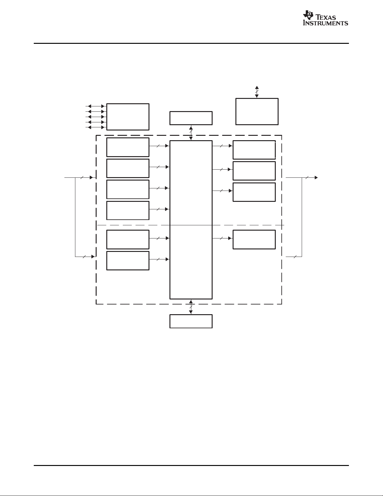
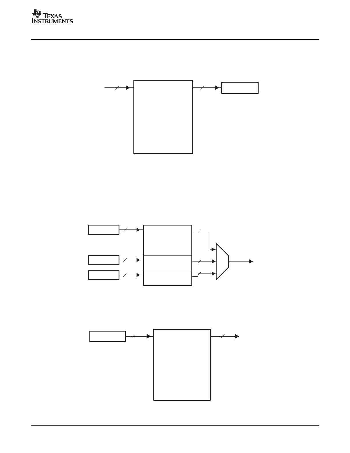
A high-level block diagram of the video port is shown in Figure 1-1 . The port consists of two channels: A
and B. You can split a 5120-byte capture/display buffer between the two channels. The entire port (both
channels) is always configured for either video capture or display only. Separate data pipelines control the
parsing and formatting of video capture or display data for each of the BT.656, Y/C, raw video, and TCI
modes.
For video capture operation, the video port may operate as two 8-bit channels of BT.656 or raw video
capture; or as a single channel of 8-bit BT.656, 8-bit raw video, 8-bit Y/C video, 16-bit raw video, or 8-bit
TCI.
For video display operation, the video port may operate as a single channel of 8-bit BT.656, 8-bit raw
video, 8-bit Y/C video, or 16-bit raw video. It may also operate in a two channel 8-bit raw mode in which
the two channels are locked to the same timing. Channel B is not used during single channel operation.
It is important to note that the VideoPort Data pin numbering is compatible with TMS320DM642 DSP
chip.In case of a 8-bit channel the suffixes for the data pins are mentioned as VDOUT[9-2]for
display/output port and VDIN[9-2]for capture/input port. In case of a 16-bit channel the suffixes for the data
pins are mentioned as VDOUT[19-2]for display/output port and VDIN[19-2]for capture/input port.
Video Port
– Capture rate of up to 80 MHZ.
– Two channels of 8-bit digital video input from a digital camera or an analog camera (using a video
decoder). Digital video input is in YCbCr 4:2:2 format with 8-bit resolution multiplexed in ITU-R
BT.656 format.
– One channel of Y/C 16-bit digital video input in YCbCr 4:2:2 format on separate Y and Cb/Cr inputs.
Supports SMPTE 260M, SMPTE 274M, SMPTE 296M, ITU-BT.1120, etc., as well as older
CCIR601 interfaces.
– YCbCr 4:2:2 to YCbCr 4:2:0 horizontal conversion and 1/2 scaling in 8-bit 4:2:2 modes.
– Direct interface for two channels of up to 8-bit or one channel of up to 16-bit raw video from A/D
converters.
– Display rate of up to 110 MHZ.
– One channel of continuous digital video output. Digital video output is YCbCr 4:2:2 co-sited pixel
data with 8-bit resolution multiplexed in ITU-R BT.656 format.
– One channel of Y/C 16-bit digital video output in YCbCr 4:2:2 format on separate Y and Cb/Cr
outputs. (Supports SMPTE 260M, SMPTE 274M, SMPTE 296M, ITU-BT.1120, etc.)
– YCbCr 4:2:0 to YCbCr 4:2:2 horizontal conversion and 2x scaling of output in 8-bit 4:2:2 modes.
– Programmable clipping of BT.656 and Y/C mode output values.
– One channel of raw data output up to 16-bits for interface to RAMDACs. Two channel synchronized
raw data output.
– Synchronizes to external video controller or another video display port.
– Using the external clock, the frame timing generator provides programmable image timing that
includes horizontal and vertical blanking, start of active video (SAV) and end of active video (EAV)
code insertion, and horizontal and frame timing pulses.
– Generates horizontal and vertical synchronization and blanking signals and a frame synchronization
signal.
a forward error correction device in 8-bit parallel format at up to 30 Mbytes/sec.
RAW and TCI mode and one interrupt to the DSP.
SPRUEM1 – May 2007 Overview 17
Submit Documentation Feedback
Page 18
www.ti.com
Internal peripheral bus
Memory
mapped
registers
Raw video
display pipeline
Channel B
Channel A
Raw video
display pipeline
Y/C video
display pipeline
BT.656 display
pipeline
Y/C video
capture pipeline
Capture/display
buffer
(2560 bytes)
Raw video
capture pipeline
BT.656 capture
pipeline
TSI capture
pipeline
Raw video
capture pipeline
VDIN[19−12]
8
VDIN[19−2]
16
DMA interface
64
Capture/display
buffer
(2560 bytes)
8
8
8
16
16
8
16
16
Timing and
control logic
VCTL2
VCTL3
VCLK1
VCTL1
VCLK2
DMA interface
8 8
64
32
VDOUT[19−12]
8
VDOUT[19−2]
16
BT.656 capture
pipeline
Video Port
This document describes the full feature set offered by the video port. See the device-specific datasheet
for details about I/O timing information.
Figure 1-1. Video Port Block Diagram
Overview 18 SPRUEM1 – May 2007
Submit Documentation Feedback
Page 19

www.ti.com
1.2 Video Port FIFO
The video port includes a FIFO to store data coming into or out from the video port. The video port
operates in conjunction with EDMA transfers to move data between the video port FIFO and external or
on-chip memory. You can program threshold settings so that EDMA events generate when the video port
FIFO reaches a certain fullness (for capture) or goes below a certain fullness (for display). You set up
EDMA Channels that are required to service the FIFO independently and are key to correct operation of
the video port. The FIFO size is relatively large to allow time for EDMA Channels to service the transfer
requests, since the device typically has many peripheral interfaces, including five video ports.
The following sections briefly describe the interaction with the EDMA and different FIFO configurations
that are used to support the various modes of the video port.
1.2.1 EDMA Interface
Video port data transfers take place using EDMA Channels. EDMA requests are based on buffer
thresholds. Since the video port does not directly source the transfer, it can not adjust the transfer size
based on buffer empty/full status. This means the EDMA transfer size is essentially fixed in the
user-programmed EDMA parameter table. The preferred transfer size is often one entire line of data
because this allows the most flexibility in terms of frame buffer line pitch (in RAM). Some modes of
operation for the highest display rates may require more frequent EDMA requests, such as on a half or
quarter line basis.
All requests are based on buffer thresholds. EDMA requests are made whenever the number of samples
in the buffer reaches the threshold value in video capture mode. In order to ensure that all data from a
capture field/frame gets emptied from the buffer, the transfer size must be equal to the threshold and the
total amount of field/frame data must be a multiple of the transfer size.
For video display operation, EDMA requests are made whenever there is at least the threshold number of
double words free in the FIFO. This means that the transfer size must be equal or smaller than the
threshold so that it fits into the available space. The field/frame size must still be a multiple of the transfer
size or there are pixels left in the buffer at the end of the field (which appear at the start of the next field).
Video Port FIFO
SPRUEM1 – May 2007 Overview 19
Submit Documentation Feedback
Page 20
www.ti.com
VDIN[9−2]
VDIN[19−12]
Capture FIFO A
Y Buffer A (1280 bytes)
Cb Buffer A (640 bytes)
8
8
64
64
Cb Buffer B (640 bytes)
Cr Buffer B (640 bytes)
CRSRCB
CBSRCB
8
8
8
8
CBSRCA
64
64
64
Capture FIFO B
Cr Buffer A (640 bytes)
YSRCB
CRSRCA
64
YSRCA
Y Buffer B (1280 bytes)
Video Port FIFO
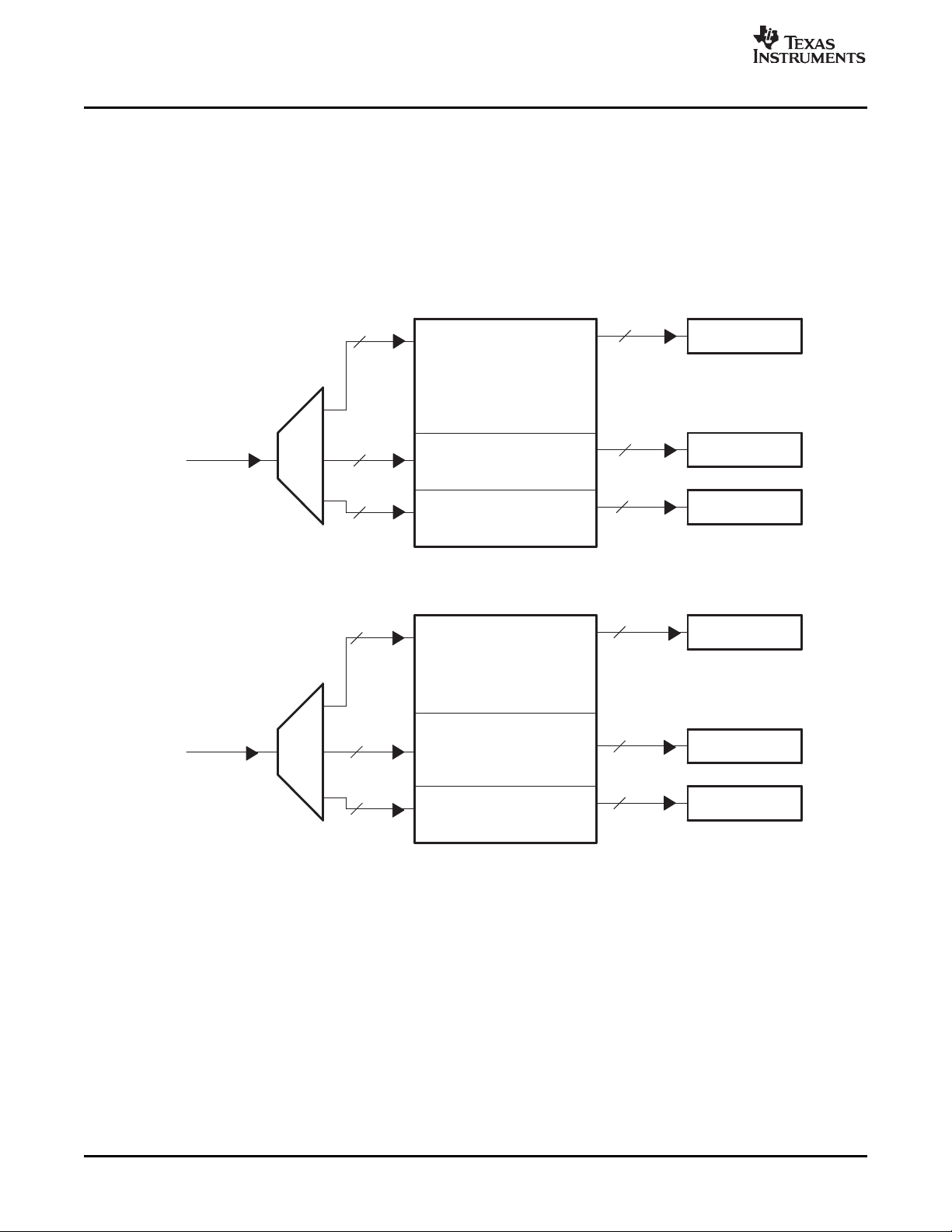
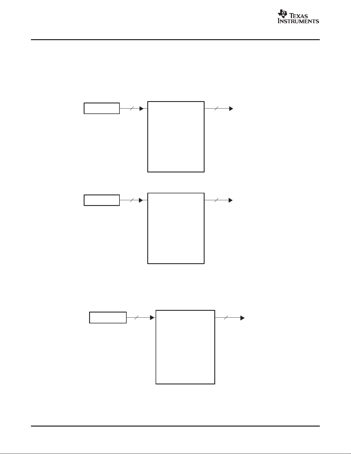
1.2.2 Video Capture FIFO Configurations
During video capture operation, the video port FIFO has one of four configurations depending on the
capture mode. For BT.656 operation, the FIFO is split into channel A and B, as shown in Figure 1-2 . Each
FIFO is clocked independently with the channel A FIFO receiving data from the VDIN[9-2] half of the bus
and the channel B FIFO receiving data from the VDIN[19-12] half of the bus. Each channel's FIFO is
further split into Y, Cb, and Cr buffers with separate write pointers and read registers (YSRC x, CBSRC x,
and CRSRC x).
Figure 1-2. BT.656 Video Capture FIFO Configuration
20 Overview SPRUEM1 – May 2007
Submit Documentation Feedback
Page 21
www.ti.com
VDIN[19−12]
8
Buffer B (2560 bytes)
Capture FIFO B
YSRCB
64
VDIN[9−2]
8
Buffer A (2560 bytes)
Capture FIFO A
YSRCA
64
Video Port FIFO
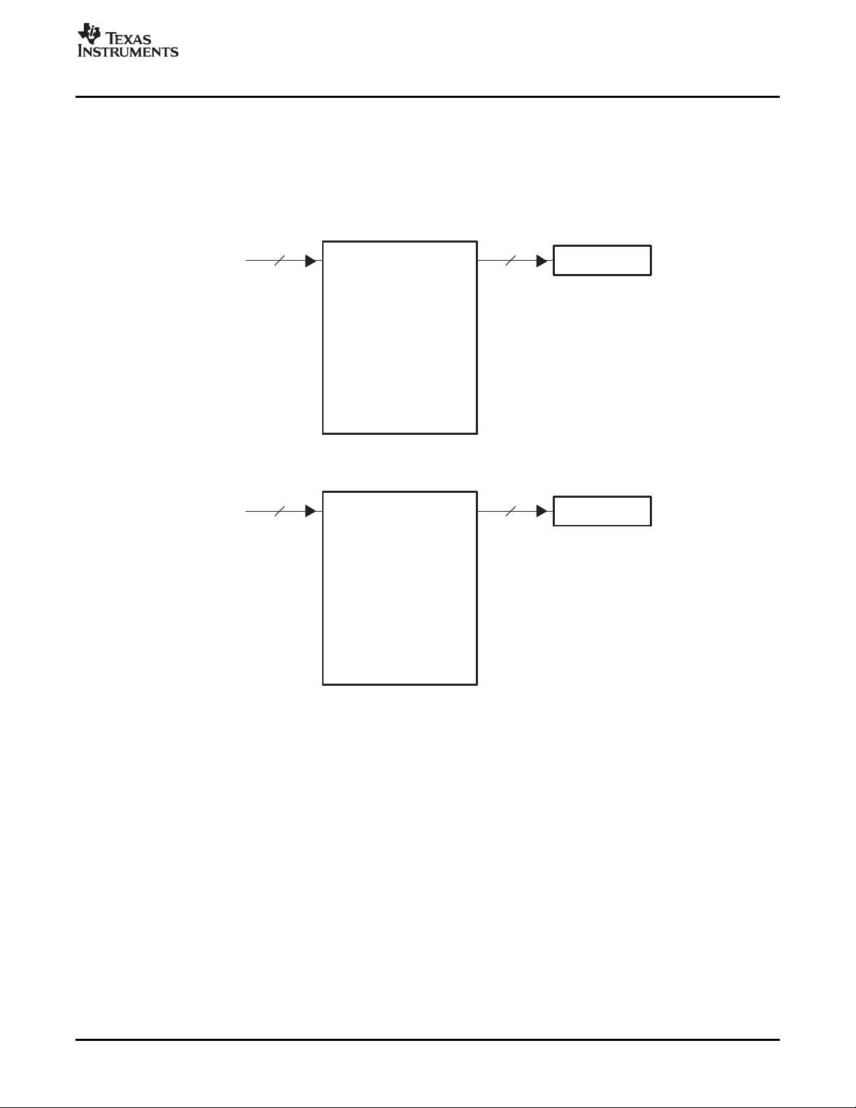
For 8-bit raw video, the FIFO is split into channel A and B, as shown in Figure 1-3 . Each FIFO is clocked
independently with the channel A FIFO receiving data from the VDIN[9-2] half of the bus and the channel
B FIFO receiving data from the VDIN[19-12] half of the bus. Each channel's FIFO has a separate write
pointer and read register (YSRC x). The FIFO configuration is identical for TCI capture, but channel B is
disabled.
Figure 1-3. 8-Bit Raw Video Capture and TCI Video Capture FIFO Configuration
SPRUEM1 – May 2007 Overview 21
Submit Documentation Feedback
Page 22
www.ti.com
VDIN[19−12]
Cr Buffer (1280 bytes)
Cb Buffer (1280 bytes)
8
8
64
64
CRSRCA
CBSRCA
Y Buffer (2560 bytes)
VDIN[9−2]
8
64
Capture FIFO
YSRCA
Video Port FIFO
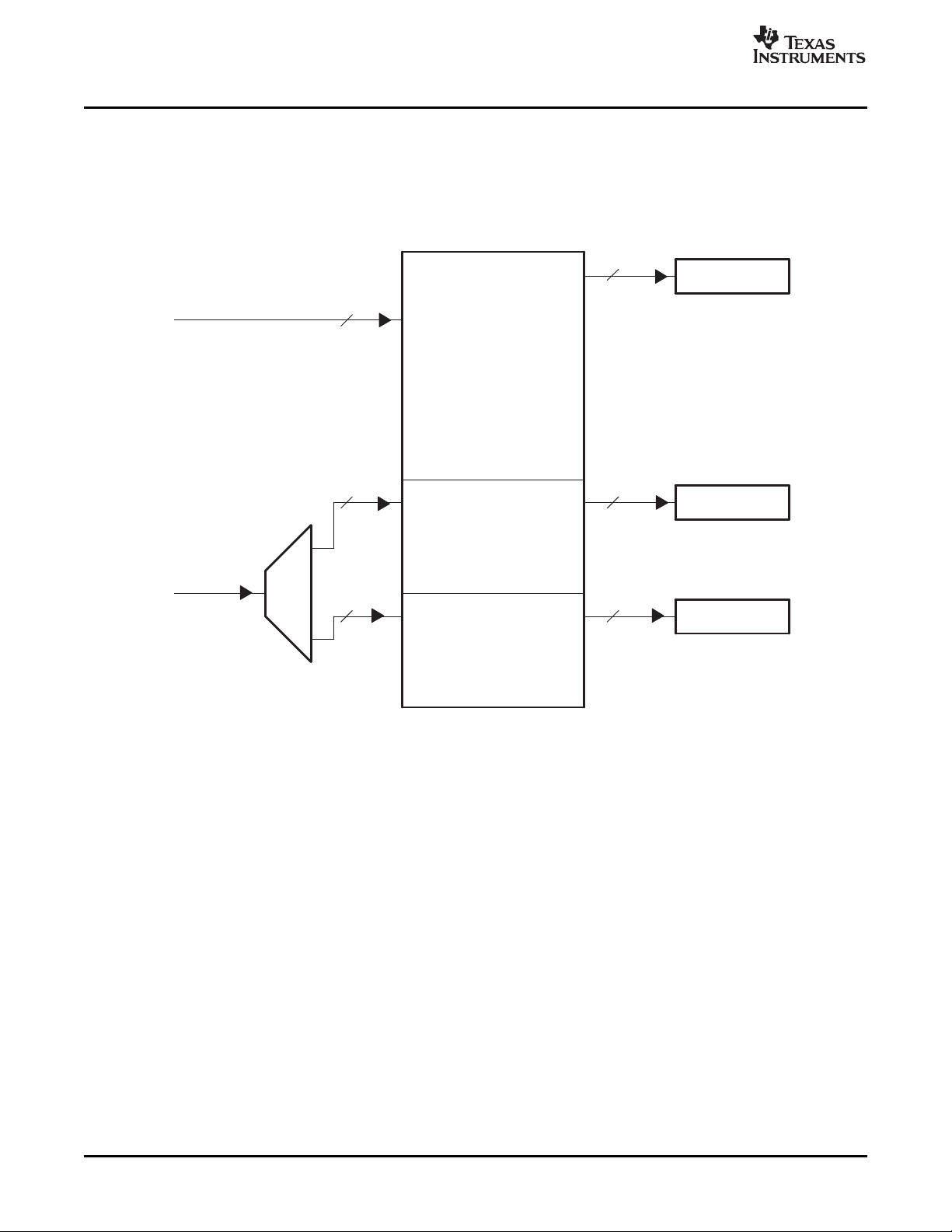
For Y/C video capture, the FIFO is configured as a single channel split into separate Y, Cb, and Cr buffers
with separate write pointers and read registers (YSRCA, CBSRCA, and CRSRCA). Figure 1-4 shows how
Y data is received on the VDIN[9-2] half of the bus and Cb/Cr data is received on the VDIN[19-12] half of
the bus and de-multiplexed into the Cb and Cr buffers.
Figure 1-4. Y/C Video Capture FIFO Configuration
22 Overview SPRUEM1 – May 2007
Submit Documentation Feedback
Page 23
www.ti.com
Data Buffer
(5120 bytes)
VDIN[19−2]
16
Capture FIFO
YSRCA
64
Y Buffer
(2560 bytes)
Cb Buffer
(1280 bytes)
Cr Buffer
(1280 bytes)
YDSTA
CBDST
CRDST
VDOUT[9−2]
Display FIFO
8
8
8
64
64
64
Data Buffer
(5120 bytes)
YDSTA
VDOUT[9−2]
64
8
Display FIFO
For 16-bit raw video, the FIFO is configured as a single buffer, as shown in Figure 1-5 . The FIFO receives
16-bit data from the VDIN[19-2] bus. The FIFO has a single write pointer and read register (YSRCA).
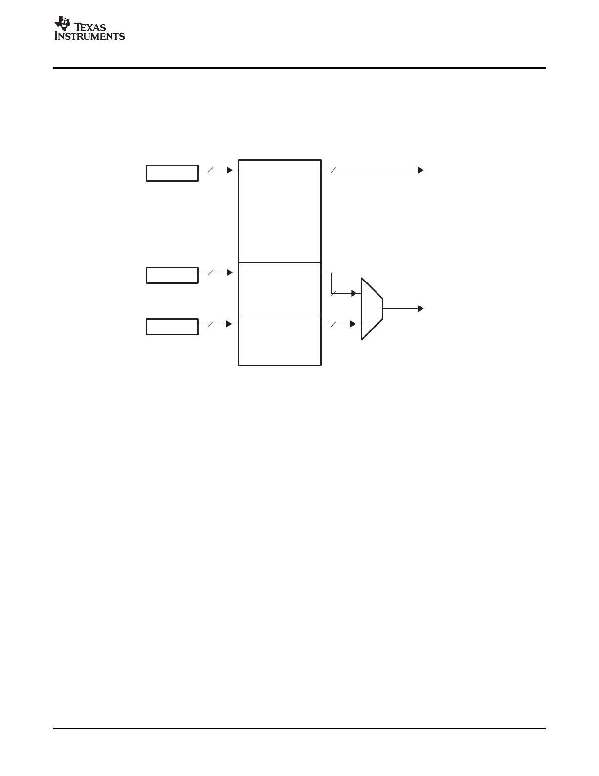
1.2.3 Video Display FIFO Configurations
During video display operation, the video port FIFO has one of five configurations depending on the
display mode. For BT.656 operation, a single output is provided on channel A, as shown in Figure 1-6 ,
with data output on VDOUT[9-2]. The channel's FIFO is split into Y, Cb, and Cr buffers with separate read
pointers and write registers (YDSTA, CBDST, and CRDST).
Video Port FIFO
Figure 1-5. 16-Bit Raw Video Capture FIFO Configuration
Figure 1-6. BT.656 Video Display FIFO Configuration
For 8-bit raw video, the FIFO is configured as a single buffer as shown in Figure 1-7 . The FIFO outputs
data on the VDOUT[9-2] half of the bus. The FIFO has a single read pointer and write register (YDSTA).
Figure 1-7. 8-Bit Raw Video Display FIFO Configuration
SPRUEM1 – May 2007 Overview 23
Submit Documentation Feedback
Page 24
www.ti.com
Buffer A (2560 bytes)
YDSTA
VDOUT[9−2]
64
8
Display FIFO A
Buffer B (2560 bytes)
YDSTB
VDOUT[19−12]
64
8
Display FIFO B
Data Buffer (5120 bytes)
YDSTA
VDOUT[19−2]
64
16
Display FIFO
Video Port FIFO
For locked raw video, the FIFO is split into channel A and B. The channels are locked together and use
the same clock and control signals. Each channel uses a single buffer and write register (YDST x) as
shown in Figure 1-8 .
For 16-bit raw video, the FIFO is configured as a single buffer, as shown in Figure 1-9 . The FIFO outputs
data on VDOUT[19-2]. The FIFO has a single read pointer and write register (YDSTA).
Figure 1-8. 8-Bit Locked Raw Video Display FIFO Configuration
Figure 1-9. 16-Bit Raw Video Display FIFO Configuration
24 Overview SPRUEM1 – May 2007
Submit Documentation Feedback
Page 25
www.ti.com
Cr Buffer (1280
bytes)
Cb Buffer
(1280 bytes)
CRDST
CBDST
64
64
VDOUT[19−12]
8
8
Y Buffer
(2560 bytes)
YDSTA
64
VDOUT[9−2]
Display FIFO
8
Video Port Registers
For Y/C video display, the FIFO is configured as a single channel split into separate Y, Cb, and Cr buffers
with separate read pointers and write registers (YDSTA, CBDST, and CRDST). Figure 1-10 shows how Y
data is output on the VDOUT[9-2] half of the bus and Cb/Cr data is multiplexed and output on the
VDOUT[19-12] half of the bus.
Figure 1-10. Y/C Video Display FIFO Configuration
1.3 Video Port Registers
The video port configuration register space is divided into several different sections with registers grouped
by function including top-level video port control, video capture control, video display control, and GPIO.
The registers for controlling the video port are in Section 2.4 .
The registers for controlling the video capture mode of operation are shown in Section 3.13 . An additional
space is dedicated for FIFO read pseudo-registers as shown in Section 3.14 . This space requires
high-speed access and is not mapped to the register access bus.
The registers for controlling the video display mode of operation are shown in Section 4.12 . An additional
space is dedicated for FIFO write pseudo-registers as shown in Section 4.14 . This space requires
high-speed access and is not mapped to the register access bus.
The registers for controlling the general-purpose input/output (GPIO) are shown in Section 5.1 .
SPRUEM1 – May 2007 Overview 25
Submit Documentation Feedback
Page 26

www.ti.com
Video Port Pin Mapping
1.4 Video Port Pin Mapping
The video port requires 21 external signal pins for full functionality. Pin usage and direction changes
depend on the selected operating mode. Pin functionality detail for video capture mode is listed in
Table 1-1 . Pin functionality detail for video display mode is listed in Table 1-2 . All unused port signals
(except VCLK1 and VCLK1) can be configured as general-purpose I/O (GPIO) pins.
Table 1-1. Video Capture Signal Mapping
Usage
BT.656 Capture Mode Raw Data Capture Mode
Video Port Signal I/O Dual Channel Channel Mode 8-Bit 16-Bit Mode
VDATA[9-2] I/O VDIN[9-2] VDIN[9-2] VDIN[9-2] VDIN[9-2] VDIN[9-2] VDIN[9-2]
VDATA[19-12] I/O VDIN[19-12] Not Used VDIN[19-12] VDIN[19-12] VDIN[19-12] Not Used
VCLK1 I VCLKINA (In) VCLKINA (In) VCLKINA (In) VCLKINA (In) VCLKINA (In) VCLKINA (In)
VCLK1 I/O VCLKINB (In) Not Used Not Used VCLKINB (In) Not Used Not Used
VCTL1 I/O CAPENA CAPENA/ CAPENA/ CAPENA CAPENA CAPENA
VCTL2 I/O CAPENB VBLNK/ VBLNK/ CAPENB Not Used PACSTRT
VCTL3 I/O Not Used FID FID FID (In) FID (In) PACERR
(1)
Legend: VCLKINA – Channel A capture clock; CAPENA – Channel A capture enable; VCLKINB – Channel B capture clock;
CAPENB – Channel B capture enable; AVID – Active video; HSYNC – Horizontal synchronization; VBLNK – Vertical blanking;
VSYNC – Vertical synchronization; FID – Field identification; PACSTRT – Packet start; PACERR – Packet error
(In) Ch A (In) Ch A (In) (Y) (In) Ch A (In) (In)
(In) Ch B (In) (Cb/Cr) (In) Ch B (In)
(In) AVID/HSYNC AVID/HSYNC (In) (In) (In)
(In) VSYNC (In) VSYNC (In) (In) (In)
Single Y/C Capture TCI Capture
(In) (In)
(In) (In) Ch A Ch A (In)
(1)
Table 1-2. Video Display Signal Mapping
Usage
Video Port Signal I/O Mode Mode 8-Bit 16-Bit 8-Bit Dual Sync
BT.656 Display Y/C Display
VDATA[9-2] I/O VDOUT[9-2] VDOUT[9-2] VDOUT[9-2] VDOUT[9-2] VDOUT[9-2]
(Out) (Out) (Y) (Out) (Out) (Out) (Ch A)
VDATA[19-12] I/O Not Used VDOUT[19-12] Not Used VDOUT[19-12] VDOUT[19-12]
(Out) (Cb/Cr) (Out) (Out) (Ch B)
VCLK1 I VCLKIN (In) VCLKIN (In) VCLKIN (In) VCLKIN (In) VCLKIN (In)
VCLK1 I/O VCLKOUT (Out) VCLKOUT (Out) VCLKOUT (Out) VCLKOUT (Out) VCLKOUT (Out)
VCTL1 I/O HSYNC/HBLNK/ HSYNC/HBLNK/ HSYNC/HBLNK/ HSYNC/HBLNK/ HSYNC/HBLNK/
AVID/FLD (Out) AVID/FLD (Out) AVID/FLD (Out) AVID/FLD (Out) AVID/FLD (Out)
or HSYNC (In) or HSYNC (In) or HSYNC (In) or HSYNC (In) or HSYNC (In)
VCTL2 I/O VSYNC/VBLNK/C VSYNC/VBLNK/C VSYNC/VBLNK/C VSYNC/VBLNK/C VSYNC/VBLNK/C
SYNC/FLD (Out) SYNC/FLD (Out) SYNC/FLD (Out) SYNC/FLD (Out) SYNC/FLD (Out)
or VSYNC (In) or VSYNC (In) or VSYNC (In) or VSYNC (In) or VSYNC (In)
VCTL3 I/O CBLNK/FLD CBLNK/FLD CBLNK/FLD CBLNK/FLD CBLNK/FLD
(Out) or FLD (In) (Out) or FLD (In) (Out) or FLD (In) (Out) or FLD (In) (Out) or FLD (In)
Raw Data Display Mode
Overview 26 SPRUEM1 – May 2007
Submit Documentation Feedback
Page 27

www.ti.com
1.4.1 VDIN Bus Usage for Capture Modes
The alignment and usage of data on the VDIN bus depends on the capture mode as shown in Table 1-3 .
Video Port Pin Mapping
Table 1-3. VDIN Data Bus Usage for Capture Modes
Capture Mode
BT.656 Y/C Raw Data
Data Bus 8-Bit 8-Bit 8-Bit 16-Bit TCI Mode
VDIN19 B A (C) B A
VDIN18 B A (C) B A
VDIN17 B A (C) B A
VDIN16 B A (C) B A
VDIN15 B A (C) B A
VDIN14 B A (C) B A
VDIN13 B A (C) B A
VDIN12 B A (C) B A
VDIN9 A A (Y) A A A
VDIN8 A A (Y) A A A
VDIN7 A A (Y) A A A
VDIN6 A A (Y) A A A
VDIN5 A A (Y) A A A
VDIN4 A A (Y) A A A
VDIN3 A A (Y) A A A
VDIN2 A A (Y) A A A
(1)
Legend: A – Channel A capture; A(C) Channel A chroma; A(Y) Channel A luma; B – Channel B capture
(1)
SPRUEM1 – May 2007 Overview 27
Submit Documentation Feedback
Page 28

www.ti.com
Video Port Pin Multiplexing
1.4.2 VDOUT Data Bus Usage for Display Modes
The alignment and usage of data on the VDOUT bus depends on the display mode as shown in
Table 1-4 .
Table 1-4. VDOUT Data Bus Usage for Display Modes
Display Mode
BT.656 Y/C Dual Sync Raw Data Raw Data
Data Bus 8-Bit 8-Bit 8-Bit 16-Bit
VDOUT19 A (C) (B) A
VDOUT18 A (C) (B) A
VDOUT17 A (C) (B) A
VDOUT16 A (C) (B) A
VDOUT15 A (C) (B) A
VDOUT14 A (C) (B) A
VDOUT13 A (C) (B) A
VDOUT12 A (C) (B) A
VDOUT9 A A (Y) A A
VDOUT8 A A (Y) A A
VDOUT7 A A (Y) A A
VDOUT6 A A (Y) A A
VDOUT5 A A (Y) A A
VDOUT4 A A (Y) A A
VDOUT3 A A (Y) A A
VDOUT2 A A (Y) A A
(1)
(1)
1.5 Video Port Pin Multiplexing
None of the five Video Port have dedicated pins associated with them. Each of the Video Port has its pins
multiplexed with other peripherals. In order to use a desired Video Port either in Capture or Display Mode,
the user would first need to program the Pin Mux Register (PINMUX) appropriately to ensure that the
multiplexed pins work as VideoPort pins. Refer to the device-specific data manual to know details of the
PINMUX Register.
1.6 VideoPort Clocking
Each of the Video Ports have a LPSC associated with them. The LPSC provides the module clock and
reset control. On power up, the LPSC's associated with Video Ports do not gate the clock required for the
Video Port to function. User would need to appropriately program the LPSC associated with Video Port to
provide the clock to the desired Video Port before trying a data transfer operation. Refer to the
device-specific manual to know LPSC Video Port association and details of LPSC registers.
Legend: A – Channel A display; A(C) Channel A chroma; A(Y) Channel A luma; B – Optional locked channel B display
28 Overview SPRUEM1 – May 2007
Submit Documentation Feedback
Page 29

SPRUEM1 – May 2007
Video Port
This chapter discusses the basic operation of the video port. Included is a discussion of
the sources and types of resets, interrupt operation, EDMA operation, external clock
inputs, video port throughput and latency, and the video port control registers.
Topic .................................................................................................. Page
2.1 Reset Operation ........................................................................ 30
2.2 Interrupt Operation .................................................................... 31
2.3 EDMA Operation ....................................................................... 32
2.4 Video Port Control Registers ...................................................... 34
SPRUEM1 – May 2007 Video Port 29
Submit Documentation Feedback
Page 30

www.ti.com
Reset Operation
2.1 Reset Operation
The video port has several sources and types of resets. The actions performed by these resets and the
state of the port following the resets is described in the following sections.
2.1.1 Power-On Reset
Power-on reset is an asynchronous hardware reset caused by a chip-level reset operation. The reset is
initiated by a power-on reset input to the video port. When the input is active, the port places all I/Os
(VD[19-2], VCTL1, VCTL2, VCTL3, and VCLK1) in a high-impedance state.
2.1.2 Peripheral Bus Reset
Peripheral bus reset is a synchronous hardware reset caused by a chip-level reset operation. The reset is
initiated by a peripheral bus reset input to the video port. This reset can be used internally (continuously
asserted) to disable the video port for low-power operation. When the input is active, the port does the
following:
• Places (keeps) all I/Os (VD[19-2], VCTL1, VCTL2, VCTL3, and VCLK1) in a high-impedance state.
• Flushes the FIFOs (resets pointers)
• Resets all port, capture, display, and GPIO registers to their default values. These may not complete
until the appropriate module clock (VCLK1, STCLK) edges occur to synchronously release the logic
from reset.
• Clears PEREN bit in PCR to 0.
• Sets VPHLT bit in VPCTL to 1.
While the peripheral remains disabled (PEREN = 0):
• VCLK1, VCLK2, and STCLK are gated off to save peripheral power.
• Peripheral bus accesses are acknowledged (RREADY/WREADY returned) to prevent EDMA lock-up.
(Any value returned on reads, data accepted or discarded on writes.)
• Peripheral bus MMR interface allows access to GPIO registers only (PID, PCR, PFUNC, PDIR, PIN,
PDOUT, PDSET, PDCLR, PIEN, PIPOL, PISTAT, and PICLR).
• Port I/Os (VD[19-2], VCTL1, VCTL2, VCTL3, and VCLK2) remain in a high-impedance state unless
enabled as GPIO by the PFUNC bits.
If software sets the PEREN bit in PCR but the VPHLT bit in VPCTL remains set:
• VCLK1, VCLK2, and STCLK are enabled to the port (allowing logic reset to complete).
• Peripheral bus accesses are acknowledged (RREADY/WREADY returned) to prevent EDMA lock-up.
(Any value returned on reads, data accepted or discarded on writes.)
• Peripheral bus MMR interface allows access to all registers.
• Port I/Os (VD[19-2], VCTL1, VCTL2, VCTL3, and VCLK2) remain in a high-impedance state unless
enabled as GPIO by the PFUNC bits.
• VPCTL bits may be set (until the VPHLT bit is cleared).
2.1.3 Software Port Reset
A software port reset may be performed on the entire video port by setting the VPRST bit in VPCTL. This
behaves identically to the peripheral bus reset except that it does not clear the PEREN bit in PCR. This
reset:
• Performs a reset on all port logic (channel logic may stay in reset until port input clock pulses occur).
• Self-clears the VPRST bit to 0 but leaves the VPHLT bit set. The VCLK1 input must be clocking in
order for this reset to take effect.
30 Video Port SPRUEM1 – May 2007
Submit Documentation Feedback
Page 31

www.ti.com
Note: The VPRST bit may take several clock cycles to clear to 0. The VPRST bit should be
polled to make sure the bit is cleared prior to writing to the video port registers.
Once the port is configured and the VPHLT bit is cleared, the setting of other VPCTL bits
(except VPRST) is disabled. The VCLK2 output may also be driven at this time, if display
mode is selected. VCTL1-3 must remain in a high-impedance state unless enabled as
GPIO, since internal/external sync is selected through VDCTL.
2.1.4 Capture Channel Reset
A software reset may be performed on a single capture channel by setting the RSTCH bit in VC xCTL. This
reset requires that the channel VCLKIN be transitioning. On capture channel reset:
• No new EDMA events are generated.
• Peripheral bus accesses are acknowledged (RREADY returned) to prevent EDMA lock-up. (Any value
returned on reads).
• Channel capture registers are set to their default values.
• Channel capture FIFO is flushed (pointers reset).
• The VCEN bit in VCxCTL is cleared to 0.
• The RSTCH bit self-clears to 0 after completion of the above.
Once the port is configured and the VCEN bit is set, the setting of other VC xCTL bits (except VCEN,
RSTCH, and BLKCAP) is prohibited and the capture counters begin counting. When BLKCAP is cleared,
data capture and event generation may begin.
Interrupt Operation
2.1.5 Display Channel Reset
A software reset may be performed on the display channel by setting the RSTCH bit in VDCTL. This reset
requires that the channel VCLKIN be transitioning. On display channel reset:
• No new EDMA events are generated.
• Peripheral bus accesses are acknowledged (WREADY returned) to prevent EDMA lock-up. (Write data
may be written into the FIFO or discarded.)
• Channel display registers are set to their default values.
• Channel display FIFO is flushed (pointers reset).
• The VDEN bit in VDCTL is cleared to 0.
• The RSTCH bit self-clears to 0 after completion of the above.
Once the port is configured and the VDEN bit is set, the setting of other VDCTL bits (except VDEN,
RSTCH, and BLKDIS) is prohibited and the display counters begin counting. Data outputs are driven (with
default value, blanking, and control codes as appropriate and any control outputs are driven). When the
BLKDIS bit is cleared, event generation may begin and FIFO data displayed.
2.2 Interrupt Operation
The video port generates an interrupt to the DSP core after any of the following events occur:
• Capture complete (CCMP x) bit is set.
• Capture overrun (COVR x) bit is set.
• Synchronization byte error (SERR x) bit is set.
• Vertical interrupt (VINT xn) bit is set.
• Short field detect (SFD x) bit is set.
• Long field detect (LFD x) bit is set.
• STC absolute time (STC) bit is set.
• STC tick counter expired (TICK) bit is set.
• Display complete (DCMP) bit is set.
• Display under-run (DUND) bit is set.
SPRUEM1 – May 2007 Video Port 31
Submit Documentation Feedback
Page 32

www.ti.com
EDMA Operation
2.3 EDMA Operation
• Display complete not acknowledged (DCNA) bit is set.
• GPIO interrupt (GPIO) bit is set.
The interrupt signal is a pulse only and does not hold state. The interrupt pulse is generated only when the
number of set flags in VPIS transitions from none to one or more. Another interrupt pulse is not generated
by setting additional flag bits.
Interrupts can be masked via the video port interrupt enable register (VPIE) using individual interrupt
enables and the VIE global enable bit. The interrupts are cleared in the video port interrupt status register
(VPIS) using the individual status bits. Writing a 1 to the appropriate bit clears the interrupt. The clearing
of an interrupt flag reenables the generation of another interrupt pulse, if other flags are still set. In other
words, pulse generation is reenabled by writing a 1 to any set bit of VPIS.
Upon receiving an interrupt you should:
1. Read VPIS.
2. Perform the service routine for whatever bits are set.
3. Clear appropriate bits by writing a 1 to their VPIS locations.
4. Upon return from the ISR, if VPIS bits have been (or remain) set, then another interrupt will occur.
The video port uses up to three EDMA events per channel for a total of six possible events. Each EDMA
event uses a dedicated event output. The outputs are:
• VPYEVTA
• VPCbEVTA
• VPCrEVTA
• VPYEVTB
• VPCbEVTB
• VPCrEVTB
2.3.1 Capture EDMA Event Generation
Capture EDMA events are generated based on the state of the capture FIFO(s). If no EDMA event is
currently pending and the FIFO crosses the value specified by VCTHRLD n, an EDMA event is generated.
Once an event has been requested, another EDMA event may not be generated until the servicing of the
outstanding event has begun (as indicated by the first read of the FIFO by the EDMA event service). If the
capture FIFO level exceeds 2x the VCTHRLD n value before the requested EDMA event completes, then
another EDMA event may be generated. Thus, up to one EDMA event may be outstanding.
An outgoing data counter counts data read by the EDMA. This counter is loaded with the VCTHRLD n
value whenever a new EDMA service begins. The counter then counts down for each double-word read
from the FIFO by the EDMA. The EDMA is complete when the counter reaches zero.
For BT.656 and Y/C modes, there are three FIFOs, one for each of the Y, Cb, and Cr color components.
Each FIFO generates its own EDMA event; therefore, the EDMA event state and FIFO thresholds for each
FIFO are tracked independently. The Cb and Cr FIFOs use a threshold value of 1/2 (VCTHRLD n +
VCTHRLD nmod 2).
Because the capture FIFOs may hold multiple thresholds worth of data, a problem arises at the
boundaries between fields. Since Field 1 and Field 2 may have different threshold values, the amount of
data in the FIFO required to generate the EDMA event changes depending on the current capture field
and the field of any outstanding EDMA requests. Similarly, the threshold value loaded in the outgoing data
counter needs to change depending on which field's EDMA event is being serviced (not which field is
currently being captured). To prevent confusion at the field boundaries, the VC xEVTCT register is
programmed to indicate the number of events to generate for each field. An event counter tracks how
many events have been generated and indicates which threshold value to use in event generation and in
the outgoing data counter. After the last Field 1 event has been generated, the EDMA logic looks for FIFO
> THRSHLD1 + THRSHLD2 to pre-generate the first Field 2 event. Once the last Field 1 event completes,
the logic looks for FIFO > 2x THRSHLD2 (assuming a Field 2 event is outstanding).
Video Port32 SPRUEM1 – May 2007
Submit Documentation Feedback
Page 33

www.ti.com
2.3.2 Display EDMA Event Generation
Display EDMA events are generated based on the amount of room available in the FIFO. The VDTHRLD n
value indicates the level at which the FIFO has room to receive another EDMA. If the FIFO has at least
VDTHRLD n locations available, a EDMA event is generated. Once an E EDMA event has been
requested, another EDMA event may not be generated until the servicing of the first EDMA event has
begun (as indicated by the first write to the FIFO by the EDMA event service). If there is at least 2x the
threshold space still available in the FIFO after the first EDMA service is begun (and the display event
counter has not expired) then another EDMA event may be generated. Thus, up to one EDMA request
may be outstanding.
An incoming data counter is loaded with the VDTHRLD n (or VDTHRLD n/2 for Cb and Cr FIFOs) value at
the beginning of each EDMA event service and counts down the incoming EDMA double words When the
counter reaches 0, the EDMA event is complete.
An EDMA event counter is used to track the number of EDMA events generated in each field as
programmed in the VDDISPEVT register. The DISPEVT1 or DISPEVT2 value (depending on the current
display field) is loaded at the start of each field. The event counter then decrements with each EDMA
event generation until it reaches 0, at which point no more EDMA events are generated until the next field
begins. Once the last line of data for a field has been requested, the EDMA logic stops generating events
until the field is complete in case the CPU needs to modify the EDMA address pointers.
For BT.656 and Y/C modes, there are three FIFOs, one for each of the Y, Cb, and Cr color components.
Each FIFO generates its own EDMA event; therefore, the EDMA event state and FIFO thresholds for each
FIFO are tracked independently. (The Cb and Cr FIFOs use a threshold value of 1/2 VDTHRLD).
EDMA Operation
2.3.3 EDMA Size and Threshold Restrictions
The video port FIFOs are 64-bits wide and always read or write 64 bits at a time. For this reason, EDMA
accesses must always be an even number of words in length. It is expected that in most cases the
threshold size is set to the line length (rounded up to the next double word). This always works because
different lines are not packed together within a double word and the Cb and Cr thresholds
(1/2 VCTHRLD x/VDTHRLD) are always rounded up to the double word.
For example, in 8-bit BT.656 capture mode with a line length of 712 (Y), setting the threshold to the line
length results in a VCTHRLD of 712 pixels x 1 bytes/pixel x double word/8 bytes = 89 double words. The
Cb and Cr FIFOs contain half the data (44.5 double words) so their thresholds are set to 45 double words.
Therefore, the Cb and Cr EDMAs each transmit an extra 4 bytes at the end of each line.
If a multi-horizontal line length threshold is desired (2 lines, for example) then the chosen line length must
round up to an even number of double words so that it is evenly divisible by 2. If this is not the case, then
the Cb and Cr FIFO transfers are corrupted. For the multiline case, consider the same 8-bit BT.656
capture mode with a line length of 712 (Y). If the threshold is set for 2 lines, this results in a VCTHRLD
value of 2 x 89 = 178 double words. The actual Cb/Cr line length is 44.5 double words that requires a
length of 45. To transfer 2 lines requires 2 x 45 = 90 double words. However, for this VCTHRLD, the
EDMA logic would calculate the Cb/Cr threshold size as 178/2 = 89 double words, which is 1 double word
off. This can be corrected by increasing the line length to 720 pixels (and ignoring the extra captured
pixels) or decreasing it to 704 pixels.
Similarly if a sub-horizontal line length is desired (1/2 line, for example), then the line length and threshold
must be chosen such that the threshold is divisible by 2. (This can also be stated as the line length must
be an even multiple of #EDMAs/line x 8). For the subline case, consider the 8-bit BT.656 capture mode
with a line length of 624 (Y). If the threshold is set for 1/2 the line length, this results in VCTHRLD =
(624/2)/8 = 39 double words. The EDMA logic would calculate the Cb/Cr threshold as 39/2 = 20 double
words. However, two such Cb/Cr EDMA events would result in a transfer of 40 double words, which is
larger than the actual Cb/Cr line length of (624/2)/8 = 39 double words. This can be corrected by changing
the line size to 640 pixels or 608 pixels, or by changing the threshold to be 1/3 the line length (VCTHRLD
= (624/3)/8 = 26 double words and the Cb/Cr threshold is 26/2 = 13 double words. 3 x 13 = 39 double
words, which is exactly the Cb/Cr line length.)
SPRUEM1 – May 2007 Video Port 33
Submit Documentation Feedback
Page 34

www.ti.com
Video Port Control Registers
2.3.4 EDMA Interface Operation
When the video port is configured for capture (or TCI) mode, it only accepts read requests from the EDMA
interface. Write requests are false acknowledged (so the bus does not stall) and the data is discarded.
When the video port is configured for display mode, it only accepts write requests. Read requests are
false acknowledged (so the bus does not stall) and an arbitrary data value is returned.
When the video port is in reset, is not enabled (PEREN bit cleared), halted (VPHALT bit is set), or the
active mode is not enabled (VCEN or VDEN bit is cleared), then the port will false acknowledge all EDMA
accesses to prevent bus lockup.
The video port EDMA event generation logic is very tightly coupled to the EDMA interface accesses. An
incorrectly programmed EDMA size causes the EDMA and FIFO to become misaligned causing
aberrations in the captured or displayed data and likely resulting in an eventual FIFO overflow or
underflow. In the same manner, if another system EDMA incorrectly addresses the video port during
active capture or display, the video port has no way of determining that this is an errant EDMA because all
it monitors is a EDMA access so it must perform the FIFO read or write. Such an errant EDMA eventually
causes the FIFO to be over-read or overwritten.
2.4 Video Port Control Registers
The video port control registers are listed in Table 2-1 . See the device-specific datasheet for the memory
address of these registers.
Offset
Address
C0h VPCTL Video Port Control Register Section 2.4.1
C4h VPSTAT Video Port Status Register Section 2.4.2
C8h VPIE Video Port Interrupt Enable Register Section 2.4.3
CCh VPIS Video Port Interrupt Status Register Section 2.4.4
Table 2-1. Video Port Control Registers
(1)
Acronym Register Name Section
(1)
The absolute address of the registers is device/port specific and is equal to the base address + offset address. See the
device-specific datasheet to verify the register addresses.
Video Port34 SPRUEM1 – May 2007
Submit Documentation Feedback
Page 35

www.ti.com
Video Port Control Registers
2.4.1 Video Port Control Register (VPCTL)
The video port control register (VPCTL) determines the basic operation of the video port.
Not all combinations of the port control bits are unique. The control bit encoding is shown in Table 2-3 .
Additional mode options are selected using the video capture channel A control register (VCACTL) and
video display control register (VDCTL).
The video port control register (VPCTL) is shown in Figure 2-1 and described in Table 2-2 .
Figure 2-1. Video Port Control Register (VPCTL)
31 16
Reserved
R-0
15 14 13 8
VPRST VPHLT Reserved
R/WS-0 R/WC-1 R-0
7 6 5 4 3 2 1 0
VCLK2P VCT3P VCT2P VCT1P Reserved TCI DISP DCHNL
R/W-0 R/W-0 R/W-0 R/W-0 R-0 R/W-0 R/W-0 R/W-0
LEGEND: R/W = Read/Write; R = Read only; WC = Write a 1 to clear; WS = Write 1 to set, a write of 0 has no effect; - n = value after reset
Table 2-2. Video Port Control Register (VPCTL) Field Descriptions
Bit field
31-16 Reserved - 0 Reserved. The reserved bit location is always read as 0. A value written to this field
15 VPRST OF( value) Video port software reset enable bit. VPRST is set by writing a 1. Writing 0 has no
14 VPHLT OF( value) Video port halt bit. This bit is set upon hardware or software reset. The other VPCTL
13-6 Reserved - 0 Reserved. The reserved bit location is always read as 0. A value written to this field
7 VCLK2P OF( value) VCLK2 pin polarity bit. Has no effect in capture mode.
6 VCT3P OF( value) VCTL3 pin polarity. Does not affect GPIO operation. If VCTL3 pin is used as a FLD
(1)
For CSL implementation, use the notation VP_VPCTL_ field_ symval
(1)
symval
DEFAULT 0 No effect.
NO
RESET 1 Flush all FIFOs and set all port registers to their initial values. VCLK1 and VCLK2 are
NONE 0 No effect.
DEFAULT 1 VPHLT is cleared.
CLEAR
DEFAULT 0
NONE
REVERSE 1 Inverts the VCLK2 output clock polarity in display mode.
DEFAULT 0 Indicates the VCTL3 control signal (input or output) is active high.
NONE
ACTIVELOW 1 Indicates the VCTL3 control signal (input or output) is active low.
(1)
Value Description
has no effect.
effect.
configured as inputs and all VDATA and VCTL pins are placed in high impedance.
Auto-cleared after reset is complete.
The VPRST bit may take several clock cycles to clear to 0. The VPRST bit should be
polled to make sure the bit is cleared prior to writing to the video port registers.
bits (except VPRST) can only be changed when VPHLT is 1. VPHLT is cleared by
writing a 1. Writing 0 has no effect.
has no effect.
input on the video capture side, then the VCTL3 polarity is not considered; the field
inverse is controlled by the FINV bit in the video capture channel x control register
(VC xCTL).
SPRUEM1 – May 2007 Video Port 35
Submit Documentation Feedback
Page 36

www.ti.com
Video Port Control Registers
Table 2-2. Video Port Control Register (VPCTL) Field Descriptions (continued)
Bit field
5 VCT2P OF( value) VCTL2 pin polarity bit. Does not affect GPIO operation.
4 VCT1P OF( value) VCTL1 pin polarity bit. Does not affect GPIO operation.
3 Reserved - 0 Reserved. The reserved bit location is always read as 0. A value written to this field
2 TCI OF( value) TCI capture mode select bit.
1 DISP OF( value) Display mode select bit. VDATA pins are configured for output. VCLK2 pin is
0 DCHNL OF( value) Dual channel operation select bit. If the DCDIS bit in VPSTAT is set, this bit is forced
(1)
symval
DEFAULT 0 Indicates the VCTL2 control signal (input or output) is active high.
NONE
ACTIVELOW 1 Indicates the VCTL2 control signal (input or output) is active low.
ACTIVEHIGH 0 Indicates the VCTL1 control signal (input or output) is active high.
NONE
ACTIVELOW 1 Indicates the VCTL1 control signal (input or output) is active low.
DEFAULT 0 TCI capture mode is disabled.
NONE
CAPTURE 1 TCI capture mode is enabled.
DEFAULT 0 Capture mode is enabled.
CAPTURE
DISPLAY 1 Display mode is enabled.
DEFAULT 0 Single-channel operation is enabled.
SINGLE
DUAL 1 Dual-channel operation is enabled.
(1)
Value Description
has no effect.
configured as VCLKOUT output.
to 0.
Table 2-3. Video Port Operating Mode Selection
VPCTL Bit
TCI DISP DCHNL Operating Mode
0 0 0 Single channel video capture. BT.656, Y/C or raw mode as selected in VCACTL. Video
0 0 1 Dual channel video capture. Either BT.656 or raw 8-bit as selected in VCACTL and
0 1 x Single channel video display. BT.656, Y/C or raw mode as selected in VDCTL. Video
1 x x Single channel TCI capture.
capture B channel not used.
VCBCTL. Option is available only if DCDIS is 0.
display B channel is only used for dual channel sync raw mode.
Video Port36 SPRUEM1 – May 2007
Submit Documentation Feedback
Page 37

www.ti.com
Video Port Control Registers
2.4.2 Video Port Status Register (VPSTAT)
The video port status register (VPSTAT) indicates the current condition of the video port.
The video port status register (VPSTAT) is shown in Figure 2-2 and described in Table 2-4 .
Figure 2-2. Video Port Status Register (VPSTAT)
31 16
Reserved
R-0
15 4 3 2 1 0
Reserved DCDIS HIDATA Reserved
R-0 R-x R-x R-0
LEGEND: R = Read only; - n = value after reset
Table 2-4. Video Port Status Register (VPSTAT) Field Descriptions
Bit field
31-4 Reserved - 0 Reserved. The reserved bit location is always read as 0. A value written to this field
3 DCDIS OF( value) Dual-channel disable bit. The default value is determined by the chip-level
2 HIDATA OF( value) High data bus half. HIDATA does not affect video port operation but is provided to
1-0 Reserved - 0 Reserved. The reserved bit location is always read as 0. A value written to this field
(1)
For CSL implementation, use the notation VP_VPSTAT_ field_ symval
(1)
symval
DEFAULT 0 Dual-channel operation is enabled.
ENABLE
DISABLE 1 Port muxing selections prevent dual-channel operation.
DEFAULT 0
NONE
USE 1 Indicates that another peripheral is using VDATA[9-2] and the video port channel A
(1)
Value Description
has no effect.
configuration.
inform you which VDATA pins may be controlled by the video port GPIO registers.
HIDATA is never set unless DCDIS is also set. The default value is determined by the
chip-level configuration.
(VDIN[9-2] or VDOUT[9-2]) is muxed onto VDATA[19-12].
has no effect.
SPRUEM1 – May 2007 Video Port 37
Submit Documentation Feedback
Page 38

www.ti.com
Video Port Control Registers
2.4.3 Video Port Interrupt Enable Register (VPIE)
The video port interrupt enable register (VPIE) enables sources of the video port interrupt to the DSP.
The video port interrupt enable register (VPIE) is shown in Figure 2-3 and described in Table 2-5 .
Figure 2-3. Video Port Interrupt Enable Register (VPIE)
31 24
Reserved
R-0
23 22 21 20 19 18 17 16
LFDB SFDB VINTB2 VINTB1 SERRB CCMPB COVRB GPIO
R/W-0 R/W-0 R/W-0 R/W-0 R/W-0 R/W-0 R/W-0 R/W-0
15 14 13 12 11 10 9 8
Reserved DCNA DCMP DUND TICK STC Reserved
R-0 R/W-0 R/W-0 R/W-0 R/W-0 R/W-0 R-0
7 6 5 4 3 2 1 0
LFDA SFDA VINTA2 VINTA1 SERRA CCMPA COVRA VIE
R/W-0 R/W-0 R/W-0 R/W-0 R/W-0 R/W-0 R/W-0 R/W-0
LEGEND: R/W = Read/Write; R = Read only; - n = value after reset
Table 2-5. Video Port Interrupt Enable Register (VPIE) Field Descriptions
Bit field
31-24 Reserved - 0 Reserved. The reserved bit location is always read as 0. A value written to this field
23 LFDB OF( value) Long field detected on channel B interrupt enable bit.
22 SFDB OF( value) Short field detected on channel B interrupt enable bit.
21 VINTB2 OF( value) Channel B field 2 vertical interrupt enable bit.
20 VINTB1 OF( value) Channel B field 1 vertical interrupt enable bit.
19 SERRB OF( value) Channel B synchronization error interrupt enable bit.
18 CCMPB OF( value) Capture complete on channel B interrupt enable bit.
(1)
symval
DEFAULT 0 Interrupt is disabled.
DISABLE
ENABLE 1 Interrupt is enabled.
DEFAULT 0 Interrupt is disabled.
DISABLE
ENABLE 1 Interrupt is enabled.
DEFAULT 0 Interrupt is disabled.
DISABLE
ENABLE 1 Interrupt is enabled.
DEFAULT 0 Interrupt is disabled.
DISABLE
ENABLE 1 Interrupt is enabled.
DEFAULT 0 Interrupt is disabled.
DISABLE
ENABLE 1 Interrupt is enabled.
DEFAULT 0 Interrupt is disabled.
DISABLE
ENABLE 1 Interrupt is enabled.
(1)
Value Description
has no effect.
(1)
For CSL implementation, use the notation VP_VPIE_ field_ symval
38 Video Port SPRUEM1 – May 2007
Submit Documentation Feedback
Page 39

www.ti.com
Video Port Control Registers
Table 2-5. Video Port Interrupt Enable Register (VPIE) Field Descriptions (continued)
Bit field
(1)
symval
17 COVRB OF( value) Capture overrun on channel B interrupt enable bit.
DEFAULT 0 Interrupt is disabled.
DISABLE
ENABLE 1 Interrupt is enabled.
16 GPIO OF( value) Video port general purpose I/O interrupt enable bit.
DEFAULT 0 Interrupt is disabled.
DISABLE
ENABLE 1 Interrupt is enabled.
15 Reserved - 0 Reserved. The reserved bit location is always read as 0. A value written to this field
14 DCNA OF( value) Display complete not acknowledged bit.
DEFAULT 0 Interrupt is disabled.
DISABLE
ENABLE 1 Interrupt is enabled.
13 DCMP OF( value) Display complete interrupt enable bit.
DEFAULT 0 Interrupt is disabled.
DISABLE
ENABLE 1 Interrupt is enabled.
12 DUND OF( value) Display under-run interrupt enable bit.
DEFAULT 0 Interrupt is disabled.
DISABLE
ENABLE 1 Interrupt is enabled.
11 TICK OF( value) System time clock tick interrupt enable bit.
DEFAULT 0 Interrupt is disabled.
DISABLE
ENABLE 1 Interrupt is enabled.
10 STC OF( value) System time clock interrupt enable bit.
DEFAULT 0 Interrupt is disabled.
DISABLE
ENABLE 1 Interrupt is enabled.
9-8 Reserved - 0 Reserved. The reserved bit location is always read as 0. A value written to this field
7 LFDA OF( value) Long field detected on channel A interrupt enable bit.
DEFAULT 0 Interrupt is disabled.
DISABLE
ENABLE 1 Interrupt is enabled.
6 SFDA OF( value) Short field detected on channel A interrupt enable bit.
DEFAULT 0 Interrupt is disabled.
DISABLE
ENABLE 1 Interrupt is enabled.
5 VINTA2 OF( value) Channel A field 2 vertical interrupt enable bit.
DEFAULT 0 Interrupt is disabled.
DISABLE
ENABLE 1 Interrupt is enabled.
4 VINTA1 OF( value) Channel A field 1 vertical interrupt enable bit.
DEFAULT 0 Interrupt is disabled.
DISABLE
ENABLE 1 Interrupt is enabled.
(1)
Value Description
has no effect.
has no effect.
SPRUEM1 – May 2007 Video Port 39
Submit Documentation Feedback
Page 40

www.ti.com
Video Port Control Registers
Table 2-5. Video Port Interrupt Enable Register (VPIE) Field Descriptions (continued)
Bit field
3 SERRA OF( value) Channel A synchronization error interrupt enable bit.
2 CCMPA OF( value) Capture complete on channel A interrupt enable bit.
1 COVRA OF( value) Capture overrun on channel A interrupt enable bit.
0 VIE OF( value) Video port global interrupt enable bit. Must be set for interrupt to be sent to DSP.
(1)
symval
DEFAULT 0 Interrupt is disabled.
DISABLE
ENABLE 1 Interrupt is enabled.
DEFAULT 0 Interrupt is disabled.
DISABLE
ENABLE 1 Interrupt is enabled.
DEFAULT 0 Interrupt is disabled.
DISABLE
ENABLE 1 Interrupt is enabled.
DEFAULT 0 Interrupt is disabled.
DISABLE
ENABLE 1 Interrupt is enabled.
(1)
Value Description
2.4.4 Video Port Interrupt Status Register (VPIS)
The video port interrupt status register (VPIS) displays the status of video port interrupts to the DSP. The
interrupt is only sent to the DSP if the corresponding enable bit in VPIE is set. All VPIS bits are cleared by
writing a 1, writing a 0 has no effect.
The video port interrupt status register (VPIS) is shown in Figure 2-4 and described in Table 2-6 .
Figure 2-4. Video Port Interrupt Status Register (VPIS)
31 24
Reserved
R-0
23 22 21 20 19 18 17 16
LFDB SFDB VINTB2 VINTB1 SERRB CCMPB COVRB GPIO
R/WC-0 R/WC-0 R/WC-0 R/WC-0 R/WC-0 R/WC-0 R/WC-0 R/WC-0
15 14 13 12 11 10 9 8
Reserved DCNA DCMP DUND TICK STC Reserved
R-0 R/WC-0 R/WC-0 R/WC-0 R/WC-0 R/WC-0 R-0
7 6 5 4 3 2 1 0
LFDA SFDA VINTA2 VINTA1 SERRA CCMPA COVRA Reserved
R/WC-0 R/WC-0 R/WC-0 R/WC-0 R/WC-0 R/WC-0 R/WC-0 R-0
LEGEND: R = Read only; WC = Write 1 to clear, a write of 0 has no effect; - n = value after reset
Table 2-6. Video Port Interrupt Status Register (VPIS) Field Descriptions
Bit field
31-24 Reserved - 0 Reserved. The reserved bit location is always read as 0. A value written to this field
(1)
symval
(1)
Value Description
has no effect.
(1)
For CSL implementation, use the notation VP_VPIS_ field_ symval
40 Video Port SPRUEM1 – May 2007
Submit Documentation Feedback
Page 41

www.ti.com
Video Port Control Registers
Table 2-6. Video Port Interrupt Status Register (VPIS) Field Descriptions (continued)
Bit field
(1)
symval
23 LFDB OF( value) Long field detected on channel B interrupt detected bit. (A long field is only detected
DEFAULT 0 No interrupt is detected.
NONE
CLEAR 1 Interrupt is detected. Bit is cleared.
22 SFDB OF( value) Short field detected on channel B interrupt detected bit.
DEFAULT 0 No interrupt is detected.
NONE
CLEAR 1 Interrupt is detected. Bit is cleared.
21 VINTB2 OF( value) Channel B field 2 vertical interrupt detected bit.
DEFAULT 0 No interrupt is detected.
NONE
CLEAR 1 Interrupt is detected. Bit is cleared.
20 VINTB1 OF( value) Channel B field 1 vertical interrupt detected bit.
DEFAULT 0 No interrupt is detected.
NONE
CLEAR 1 Interrupt is detected. Bit is cleared.
19 SERRB OF( value) Channel B synchronization error interrupt detected bit.
DEFAULT 0 No interrupt is detected.
NONE
CLEAR 1 Interrupt is detected. Bit is cleared.
18 CCMPB OF( value) Capture complete on channel B interrupt detected bit. (Data is not in memory until the
DEFAULT 0 No interrupt is detected.
NONE
CLEAR 1 Interrupt is detected. Bit is cleared.
(1)
Value Description
when the VRST bit in VCBCTL is cleared to 0; when VRST = 1, a long field is always
detected.)
BT.656 or Y/C capture mode - LFDB is set when long field detection is enabled and
VCOUNT is not reset before VCOUNT = YSTOP + 1.
Raw data mode, or TCI capture mode or display mode - Not used.
BT.656 or Y/C capture mode - SFDB is set when short field detection is enabled and
VCOUNT is reset before VCOUNT = YSTOP.
Raw data mode, or TCI capture mode or display mode - Not used.
BT.656 or Y/C capture mode - VINTB2 is set when a vertical interrupt occurred in field
2.
Raw data mode or TCI capture mode - Not used.
BT.656 or Y/C capture mode - VINTB1 is set when a vertical interrupt occurred in field
1.
Raw data mode or TCI capture mode - Not used.
BT.656 or Y/C capture mode - Synchronization parity error on channel B. An SERRB
typically requires resetting the channel (RSTCH) or the port (VPRST).
Raw data mode or TCI capture mode - Not used.
EDMA transfer is complete.)
BT.656 or Y/C capture mode - CCMPB is set after capturing an entire field or frame
(when F1C, F2C, or FRMC in VCBSTAT are set) depending on the CON, FRAME,
CF1, and CF2 control bits in VCBCTL.
Raw data mode - RDFE is not set, CCMPB is set when FRMC in VCBSTAT is set
(when the data counter = the combined VCYSTOP/VCXSTOP value).
TCI capture mode - CCMPB is set when FRMC in VCBSTAT is set (when the data
counter = the combined VCYSTOP/VCXSTOP value).
SPRUEM1 – May 2007 Video Port 41
Submit Documentation Feedback
Page 42

www.ti.com
Video Port Control Registers
Table 2-6. Video Port Interrupt Status Register (VPIS) Field Descriptions (continued)
Bit field
(1)
symval
17 COVRB OF( value) Capture overrun on channel B interrupt detected bit. COVRB is set when data in the
DEFAULT 0 No interrupt is detected.
NONE
CLEAR 1 Interrupt is detected. Bit is cleared.
16 GPIO OF( value) Video port general purpose I/O interrupt detected bit.
DEFAULT 0 No interrupt is detected.
NONE
CLEAR 1 Interrupt is detected. Bit is cleared.
15 Reserved - 0 Reserved. The reserved bit location is always read as 0. A value written to this field
14 DCNA OF( value) Display complete not acknowledged. Indicates that the F1D, F2D, or FRMD bit that
DEFAULT 0 No interrupt is detected.
NONE
CLEAR 1 Interrupt is detected. Bit is cleared.
13 DCMP OF( value) Display complete. Indicates that the entire frame has been driven out of the port. The
DEFAULT 0 No interrupt is detected.
NONE
CLEAR 1 Interrupt is detected. Bit is cleared.
12 DUND OF( value) Display under-run. Indicates that the display FIFO ran out of data.
DEFAULT 0 No interrupt is detected.
NONE
CLEAR 1 Interrupt is detected. Bit is cleared.
11 TICK OF( value) System time clock tick interrupt detected bit.
DEFAULT 0 No interrupt is detected.
NONE
CLEAR 1 Interrupt is detected. Bit is cleared.
10 STC OF( value) System time clock interrupt detected bit.
DEFAULT 0 No interrupt is detected.
NONE
CLEAR 1 Interrupt is detected. Bit is cleared.
9-8 Reserved - 0 Reserved. The reserved bit location is always read as 0. A value written to this field
(1)
Value Description
FIFO was overwritten before being read out (by the EDMA).
has no effect.
caused the display complete interrupt was not cleared prior to the start of the next
gating field or frame.
EDMA complete interrupt can be used to determine when the last data has been
transferred from memory to the FIFO.
DCMP is set after displaying an entire field or frame (when F1D, F2D or FRMD in
VDSTAT are set) depending on the CON, FRAME, DF1, and DF2 control bits in
VDCTL.
BT.656, Y/C capture mode or raw data mode - Not used.
TCI capture mode -TICK is set when the TCKEN bit in TCICTL is set and the desired
number of system time clock ticks has occurred as programmed in TCITICKS.
BT.656, Y/C capture mode or raw data mode - Not used.
TCI capture mode - STC is set when the system time clock reaches an absolute time
as programmed in TCISTCMPL and TCISTCMPM registers and the STEN bit in
TCICTL is set.
has no effect.
42 Video Port SPRUEM1 – May 2007
Submit Documentation Feedback
Page 43

www.ti.com
Video Port Control Registers
Table 2-6. Video Port Interrupt Status Register (VPIS) Field Descriptions (continued)
Bit field
(1)
symval
7 LFDA OF( value) Long field detected on channel A interrupt detected bit. (A long field is only detected
DEFAULT 0 No interrupt is detected.
NONE
CLEAR 1 Interrupt is detected. Bit is cleared.
6 SFDA OF( value) Short field detected on channel A interrupt detected bit.
DEFAULT 0 No interrupt is detected.
NONE
CLEAR 1 Interrupt is detected. Bit is cleared.
5 VINTA2 OF( value) Channel A field 2 vertical interrupt detected bit.
DEFAULT 0 No interrupt is detected.
NONE
CLEAR 1 Interrupt is detected. Bit is cleared.
4 VINTA1 OF( value) Channel A field 1 vertical interrupt detected bit.
DEFAULT 0 No interrupt is detected.
NONE
CLEAR 1 Interrupt is detected. Bit is cleared.
3 SERRA OF( value) Channel A synchronization error interrupt detected bit.
DEFAULT 0 No interrupt is detected.
NONE
CLEAR 1 Interrupt is detected. Bit is cleared.
2 CCMPA OF( value) Capture complete on channel A interrupt detected bit. (Data is not in memory until the
DEFAULT 0 No interrupt is detected.
NONE
CLEAR 1 Interrupt is detected. Bit is cleared.
(1)
Value Description
when the VRST bit in VCACTL is cleared to 0; when VRST = 1, a long field is always
detected.)
BT.656 or Y/C capture mode - LFDA is set when long field detection is enabled and
VCOUNT is not reset before VCOUNT = YSTOP + 1.
Raw data mode, or TCI capture mode or display mode - Not used.
BT.656 or Y/C capture mode - SFDA is set when short field detection is enabled and
VCOUNT is reset before VCOUNT = YSTOP.
Raw data mode, or TCI capture mode or display mode - Not used.
BT.656, or Y/C capture mode or any display mode - VINTA2 is set when a vertical
interrupt occurred in field 2.
Raw data mode or TCI capture mode - Not used.
BT.656, or Y/C capture mode or any display mode - VINTA1 is set when a vertical
interrupt occurred in field 1.
Raw data mode or TCI capture mode - Not used.
BT.656 or Y/C capture mode - Synchronization parity error on channel A. An SERRA
typically requires resetting the channel (RSTCH) or the port (VPRST).
Raw data mode or TCI capture mode - Not used.
EDMA transfer is complete.)
BT.656 or Y/C capture mode - CCMPA is set after capturing an entire field or frame
(when F1C, F2C, or FRMC in VCASTAT are set) depending on the CON, FRAME,
CF1, and CF2 control bits in VCACTL.
Raw data mode - If RDFE bit is set, CCMPA is set when F1C, F2C, or FRMC in
VCASTAT is set (when the data counter = the combined VCYSTOP/VCXSTOP value)
depending on the CON, FRAME, CF1, and CF2 control bits in VCACTL. If RDFE bit is
not set, CCMPA is set when FRMC in VCASTAT is set (when the data counter = the
combined VCYSTOP/VCXSTOP value)
TCI capture mode - CCMPA is set when FRMC in VCASTAT is set (when the data
counter = the combined VCYSTOP/VCXSTOP value).
SPRUEM1 – May 2007 Video Port 43
Submit Documentation Feedback
Page 44

www.ti.com
Video Port Control Registers
Table 2-6. Video Port Interrupt Status Register (VPIS) Field Descriptions (continued)
Bit field
(1)
symval
1 COVRA OF( value) Capture overrun on channel A interrupt detected bit. COVRA is set when data in the
DEFAULT 0 No interrupt is detected.
NONE
CLEAR 1 Interrupt is detected. Bit is cleared.
0 Reserved - 0 Reserved. The reserved bit location is always read as 0. A value written to this field
(1)
Value Description
FIFO was overwritten before being read out (by the EDMA).
has no effect.
Video Port44 SPRUEM1 – May 2007
Submit Documentation Feedback
Page 45

SPRUEM1 – May 2007
Video Capture Port
Video capture works by sampling video data on the input pins and saving it to the video
port FIFO. When the amount of captured data reaches a programmed threshold level,
an EDMA is performed to move data from the FIFO into DSP memory. In some cases,
color separation is performed on the incoming video data requiring multiple FIFOs and
EDMAs to be used.
The video port enables capture of both interlaced and progressive scan data. Interlaced
capture can be performed on either a field-by-field or a frame-by-frame basis. A capture
window specifies the data to be captured within each field. Frame and field
synchronization can be performed using embedded sync codes or configurable control
inputs allowing glueless interface to various encoders and ADCs.
Topic .................................................................................................. Page
3.1 Video Capture Mode Selection .................................................... 46
3.2 BT.656 Video Capture Mode ....................................................... 46
3.3 Y/C Video Capture Mode ............................................................ 50
3.4 BT.656 and Y/C Mode Field and Frame Operation ......................... 51
3.5 Video Input Filtering .................................................................. 57
3.6 Ancillary Data Capture ............................................................... 60
3.7 Raw Data Capture Mode ............................................................. 61
3.8 TCI Capture Mode ..................................................................... 63
3.9 Capture Line Boundary Conditions ............................................. 67
3.10 Capturing Video in BT.656 or Y/C Mode ....................................... 67
3.11 Capturing Video in Raw Data Mode ............................................. 68
3.12 Capturing Data in TCI Capture Mode ........................................... 69
3.13 Video Capture Registers ............................................................ 70
3.14 Video Capture FIFO Registers .................................................... 91
SPRUEM1 – May 2007 Video Capture Port 45
Submit Documentation Feedback
Page 46

www.ti.com
Video Capture Mode Selection
3.1 Video Capture Mode Selection
The video capture module operates in one of five modes as listed in Table 3-1 . The transport channel
interface (TCI) selection is made using the TCI bit in the video port control register (VPCTL). The CMODE
bits are in the video capture channel x control register (VC xCTL). The Y/C and 16-bit raw capture modes
may only be selected for channel A and only if the DCDIS bit in VPCTL is cleared to 0.
When operating as a raw video capture channel, no data selection or data interpretation is performed. The
16-bit raw capture mode is designed to accept data from A/D converters with resolution higher than eight
bits (used, for example, in medical imaging).
TCI Bit CMODE Bits Mode Description
0 000 8-Bit ITU-R BT.656 Capture Digital video input is in YCbCr 4:2:2 with 8-bit resolution
0 010 8-Bit Raw Capture Raw 8-bit data capture at sampling rates up to 80 MHZ.
0 100 8-Bit Y/C Capture Digital video input is in YCbCr 4:2:2 with 8-bit resolution on
0 110 16-Bit Raw Capture Raw 16-bit data capture at sampling rates up to 80 MHZ.
1 010 TCI Capture 8-bit parallel TCI capture at rates up to 30 MHZ.
3.2 BT.656 Video Capture Mode
The BT.656 capture mode captures 8-bit 4:2:2 luma and chroma data multiplexed into a single data
stream. Video data is conveyed in the order Cb, Y, Cr, Y, Cb, Y, Cr, etc. where the sequence Cb, Y, Cr
refers to co-sited luma and chroma samples and the following Y value corresponds to the next luminance
sample. The data stream is de-multiplexed and each component is written in packed form into separate
FIFOs for transfer into Y, Cb, and Cr buffers in DSP memory. (This is commonly called planar format).
Table 3-1. Video Capture Mode Selection
multiplexed in ITU-R BT.656 format.
parallel Y and Cb/Cr multiplexed channels.
In BT.656 video capture mode, data bytes in which the 8 bits are all set to 1 (FFh) or are all set to 0 (00h)
are reserved for data identification purposes and consequently, only 254 of the possible 256 8-bit words
may be used to express signal value.
3.2.1 BT.656 Capture Channels
In dual channel operation, the video port can support capture of two BT.656 data streams or one BT.656
data stream and one raw data stream. In the latter case, the BT.656 stream may occur on either Channel
A or Channel B. In either case, the BT.656 stream(s) must have embedded timing reference codes and
the appropriate VCTL input must be used as a CAPEN signal.
If the port is configured for single channel operation, capture will take place on Channel A only. The
unused half of the VDATA bus may be used for GPIO or for another peripheral function. For single
channel operation, non-standard BT.656 data streams without embedded timing reference codes are
supported through the use of the timing control (VCTL) input signals.
3.2.2 BT.656 Timing Reference Codes
For standard digital video, there are two reference signals, one at the beginning of each video data block
(start of active video, SAV), and one at the end of each video block (end of active video, EAV).
(Technically each line begins with the EAV code and ends just before the subsequent EAV code.) Each
timing reference signal consists of a four sample sequence in the following format: FFh, 00h, 00h, XYh.
(The FFh and 00h values are reserved for use in these timing reference signals.) The first three bytes are
a fixed preamble. The fourth byte contains information defining field identification, the state of field
blanking and state of line blanking. The assignment of these bits within the timing reference signal is listed
in Table 3-2 .
46 Video Capture Port SPRUEM1 – May 2007
Submit Documentation Feedback
Page 47

www.ti.com
BT.656 Video Capture Mode
Table 3-2. BT.656 Video Timing Reference Codes
Data Bit 1stByte (FFh) 2ndByte (00h) 3rdByte (00h) 4thByte (XYh)
9 (MSB) 1 0 0 1
8 1 0 0 F (field)
7 1 0 0 V (vertical blanking)
6 1 0 0 H (horizontal blanking)
5 1 0 0 P3 (protection bit 3)
4 1 0 0 P2 (protection bit 2)
3 1 0 0 P1 (protection bit 1)
2 1 0 0 P0 (protection bit 0)
(1)
F = 0 during Field 1; F = 1 during Field 2
(2)
V = 0 elsewhere; V = 1 during field blanking
(3)
H = 0 in SAV; H = 1 in EAV
(4)
P0, P1, P2, and P3: Depends on F, V, and H state.
(1)
(2)
(3)
(4)
(4)
(4)
(4)
Bits P0, P1, P2, and P3 have different states depending on the state of bits F, V, and H as shown in
Table 3-3 .
Table 3-3. BT.656 Protection Bits
Line Information Bits Protection Bits
F V H P3 P2 P1 P0
0 0 0 0 0 0 0
0 0 1 1 1 0 1
0 1 0 1 0 1 1
0 1 1 0 1 1 0
1 0 0 0 1 1 1
1 0 1 1 0 1 0
1 1 0 1 1 0 0
1 1 1 0 0 0 1
The protection bits allow the port to implement a DEDSEC (double error detection, single error correction)
function on the received video timing reference code. The corrected values for the F, H, and V bits based
on the protection bit values are shown in Table 3-4 . The - entries indicate detected double bit errors that
cannot be corrected. Detection of these errors causes the SERR x bit in the video port interrupt status
register (VPIS) to be set.
Table 3-4. Error Correction by Protection Bits
Received F, V, and H Bits
Received P3-P
0000 000 000 000 - 000 - - 111
0001 000 - - 111 - 111 111 111
0010 000 - - 011 - 101 - 0011 - - 010 - 100 - - 111
0100 000 - - 011 - - 110 0101 - 001 - - 100 - - 111
0110 - 011 011 011 100 - - 011
0111 100 - - 011 100 100 100 1000 000 - - - - 101 110 1001 - 001 010 - - - - 111
1010 - 101 010 - 101 101 - 101
SPRUEM1 – May 2007 Video Capture Port 47
Submit Documentation Feedback
Bits 000 001 010 011 100 101 110 111
0
Page 48

www.ti.com
Capture Image
Ystart
Xstart
Ystop
Xstop
Field 1
Capture Image
Ystart
Xstart
Ystop
Xstop
Field 2
Hcount=0
Ycount=1
Ycount=1
BT.656 Video Capture Mode
Table 3-4. Error Correction by Protection Bits (continued)
Received P3-P
1011 010 - 010 010 - 101 010 1100 - 001 110 - 110 - 110 110
1101 001 001 - 001 - 001 110 1110 - - - 011 - 101 110 1111 - 001 010 - 100 - - -
Bits 000 001 010 011 100 101 110 111
0
3.2.3 BT.656 Image Window and Capture
The BT.656 format is an interlaced format consisting of two fields. The video port allows capture of one or
both fields. The captured image is a subset of each field and can be larger or smaller than the active video
region. The captured image position is defined by the VC xSTRT1 and VC xSTOP1 registers for field 1, and
the VC xSTRT2 and VC xSTOP2 registers for field 2. The VCXSTART and VCXSTOP bits set the
horizontal window position for the field relative to the HCOUNT pixel counter. The VCYSTART and
VCYSTOP bits set the vertical position relative to the VCOUNT line counter. This is shown in Figure 3-1 .
HCOUNT increments on every chroma sample period (every other VCLKIN rising edge) for which capture
is enabled. Once VCOUNT = YSTART, line capture begins when HCOUNT = XSTART. It continues until
HCOUNT = XSTOP. A field's capture is complete when HCOUNT = VCXSTOP and VCOUNT =
VCYSTOP.
Received F, V, and H Bits
Figure 3-1. Video Capture Parameters
Table 3-5 shows common digital camera standards and the number of fields per second, number of active
lines per field, and the number of active pixels per line.
48 Video Capture Port SPRUEM1 – May 2007
Submit Documentation Feedback
Page 49

www.ti.com
BT.656 Video Capture Mode
Table 3-5. Common Video Source Parameters
Video Source (Field 1/Field 2) Number of Active Pixels Field Rate (Hz)
square pixel 240/240 640 60
60 Hz/525 lines
BT.601 244/243 720 60
60 Hz/525 lines
square pixel 288/288 768 50
50Hz/625 lines
BT.601 288/288 720 50
50 Hz/625 lines
Number of Active Lines
For the BT.656 video capture mode, the FIFO buffer is divided into three sections (three buffers). One
section is 1280 bytes deep and is dedicated for storage of Y data samples. The other two sections are
dedicated for storage of Cb and Cr data samples, respectively. The buffers for Cb and Cr samples are
each 640 bytes deep. The incoming video data stream is separated into Y, Cb, and Cr data streams,
scaled (if selected), and the Y, Cb, and Cr buffers are filled. Each of the three buffers has a
memory-mapped location associated with it; YSRC, CBSRC, and CRSRC. The YSRC, CBSRC, and
CRSRC locations are read only and are used by EDMAs to access video data samples stored in the
FIFOs.
If video capture is enabled (BLKCAP bit in VC xCTL is cleared), pixels in the capture window are captured
in the Y, Cb, and Cr buffers. The video capture module uses the YEVT, CbEVT, and CrEVT events to
notify the EDMA controller to copy data from the capture buffers to the DSP memory. The number of
double words required to generate the events is set by the VCTHRLD n bits in VC xTHRLD. On every
YEVT, the EDMA should move data from the Y buffer to DSP memory using the YSRC location as the
source address. On every CbEVT, the EDMA should move data from the Cb buffer to DSP memory using
the CBSRC location as the source address. On every CrEVT, the EDMA should move data from the Cr
buffer to DSP memory using the CRSRC location as the source address. Note that transfer size from the
Cb and Cr buffers is half of the transfer size from the Y buffer since for every four Y samples, there are
two Cb and two Cr samples.
3.2.4 BT.656 Data Sampling
Incoming data (including timing codes) are sampled and the HCOUNT counter advanced only on clock
cycles for which the CAPEN input is active. Inputs when CAPEN is inactive are ignored. The timing
reference codes are recognized only when three sequential samples with CAPEN valid are the FFh, 00h,
00h sequence. A non-00h sample after the FFh or after the first 00h causes the timing reference
recognition logic to be reset and to look for FFh again. (Unsampled data; those with CAPEN inactive; in
the middle of a timing reference do not cause the recognition logic to be reset since these are not
considered to be valid inputs.)
3.2.5 BT.656 FIFO Packing
Captured data is always packed into 64-bits before being written into the capture FIFO(s).By default, data
is packed into the FIFO from right to left.
The 8-bit BT.656 mode uses three FIFOs for color separation. Samples are packed into each word as
shown in Figure 3-2 .
SPRUEM1 – May 2007 Video Capture Port 49
Submit Documentation Feedback
Page 50

www.ti.com
Cr 1
Cr 9
Cb 1
Cb 9
Y 1
Y 9
Y 17
Y 25
Cr 2
Cr FIFO
Little-Endian Packing
Cr 6
Cr 14
Cb 6
Cb 14
Y 6
Y 14
Y 22
Y 30
Cb 0
Y 23
Cr 7
Cr 15
63
Cb 7
Cb 15
63
Y 7
Y 15
Cb FIFO
Y FIFO
5556
5556
Y 31
63
VCLKINA / VCLKINB
VDIN[9−2] / VDIN[9−12]
5556
Cr 4
Cr 12
Cb 4
Cb 12
Y 4
Y 12
Y 20
Y 28
Y 2
Y 21
Cr 5
Cr 13
Cb 5
Cb 13
Y 5
Y 13
48 47
48 47
3940
40 39
Y 29
Cr 0Y 0
48 47
Cb 1
40 39
Y 1
Y 18Y 19
Cr 2
Cr 10
23
Cb 2
Cb 10
23
Y 2
Y 10
Cb 11
Cr 3
Cr 11
Cb 3
3132 24
Y 3
Y 11
3132 24
1516
1516
Y 26
23
Y 3
Y 27
Cr 1
3132
24
Y 4Cb 2
1516
Y 16
Cr 0
Cr 8
Cb 0
Cb 8
Y 0
Y 8
8 7
8 7
0
0
Y 24
Y 5
8 7 0
Y/C Video Capture Mode
3.3 Y/C Video Capture Mode
The Y/C capture mode is similar to the BT.656 capture mode but captures 8-bit 4:2:2 data on separate
luma and chroma data streams. One data stream contains Y samples and the other stream contains
multiplexed Cb and Cr samples co-sited with every other Y sample. The Y samples are written into a Y
FIFO and the chroma samples are de-multiplexed and written into separate Cb and Cr FIFOs for transfer
into Y, Cb, and Cr buffers in DSP memory.
The Y/C capture mode supports HDTV standards such as SMPTE260, SMPTE296, and BT.1120 with
embedded EAV and SAV codes. It also supports SDTV YCbCr modes that use separate control signals
(sometimes called CCIR601 mode)
As with the BT.656 capture mode, data bytes where the 8 most-significant bits are all set to 1 (FFh) or are
all cleared to 0 (00h) are reserved for data identification purposes and consequentially only 254 of the
possible 256 8-bit words may be used to express signal value.
Figure 3-2. 8-Bit BT.656 FIFO Packing
3.3.1 Y/C Capture Channels
3.3.2 Y/C Timing Reference Codes
3.3.3 Y/C Image Window and Capture
50 Video Capture Port SPRUEM1 – May 2007
Because Y/C mode requires the entire VDATA bus, only single channel operation is supported. If the
DCHDIS bit in VPCTL is set, then Y/C mode cannot be selected. Y/C capture takes place on channel A
only. Both embedded timing references and external control inputs are supported.
Many high-resolution Y/C interface standards provide for embedded timing reference codes. These codes
are identical to those used in the BT.656 standard except that they appear on both the luma (Y) and
chroma (CbCr) data streams in parallel.
The SDTV Y/C format (CCIR601) is an interlaced format consisting of two fields just like BT.656. HDTV
Y/C formats may be interlaced or progressive scan. For interlaced capture, the capture windows are
programmed identically to BT.656 mode. For progressive scan formats, only field1 is used.
In Y/C mode, HCOUNT increments on every luma sample period (every VCLKINA rising edge) for which
capture is enabled. Once YCOUNT = YSTART, line capture begins when HCOUNT = XSTART. It
continues until HCOUNT = XSTOP. A field's capture is complete when HCOUNT = VCXSTOP and
VCOUNT = VCYSTOP.
Submit Documentation Feedback
Page 51

www.ti.com
Cr 9
Cr 1
Cb 9
Cb 1
Y 9
Y 1
Y 25
Y 17
Cb 5
Y 10
Little-Endian Packing
Cr 14
Cr 6
Y 0
Cb 0
Cb 14
Cb 6
Y 14
Y 6
Y 30
Y 22Y 23
Cr 15
Cr 7
Cb 15
Cb 7
Y 15
Y 7
Cr FIFO
Cb FIFO
63
Y FIFO
63
5556
5556
Y 31
63
VDIN[19−12]
5556
VCLKINA
VDIN[9−2]
Cr 11
Cr 3
Cb 11
Cb 3
Y 11
Y 3
Y 27
Y 19
Cr 2
Y 5
Y 20Y 21
Cr 13
Cr 5
40
40
Cb 13
Cb 5
Y 13
Y 5
4748
48 47
Cb 12
Cr 12
Cr 4
Cb 4
39 3231
Y 12
Y 4
39 3231
Cb 1
Y 29
40
Y 2
Cr 0
48 47
Y 1
Cb 2
Y 28
39
Cr 1
32 31
Y 4Y 3
Y 18
Cr 10
Cr 2
Cb 10
Cb 2
Y 10
Y 2
2324
2324
1516
1516
Y 26
Cr 3
Y 7
Cb 3
2324
Y 6
1516
Cb 4
Y 9Y 8
Y 16
Cr 8
Cr 0
0
Cb 8
Cb 0
0
Y 8
Y 0
78
8 7
Y 24
0
Cr 5
8 7
Y 11
Cb 4
For the Y/C video capture mode, the FIFO buffer is divided into three sections (three buffers). One section
is 2560 bytes deep and is dedicated for storage of Y data samples. The other two sections are dedicated
for storage of Cb and Cr data samples, respectively. The buffers for Cb and Cr samples are each 1280
bytes deep. The incoming video data stream is separated into Y, Cb, and Cr data streams, scaled (if
selected) and the Y, Cb, and Cr buffers are filled. Each of the three buffers has a memory-mapped
location associated with it; YSRC, CBSRC, and CRSRC. The YSRC, CBSRC, and CRSRC locations are
read only and are used by EDMAs to access video data samples stored in the FIFOs. Reads must always
be 64 bits.
If video capture is enabled, pixels in the capture window are captured in the Y, Cb, and Cr buffers. The
video capture module uses the YEVT, CbEVT, and CrEVT events to notify the EDMA controller to copy
data from the capture buffers to the DSP memory. The number of pixels required to generate the events is
set by the VCTHRLD n bits in VC xCTL (the VCTHRLD n value must be an even number for Y/C mode).
The capture module generates the events after VCTHRLD new pixels have been received. On every
YEVT, the EDMA should move data from the Y buffer to DSP memory using the YSRC register as the
source address. On every CbEVT, the EDMA should move data from the Cb buffer to DSP memory using
the CBSRC register as the source address. On every CrEVT, the EDMA should move data from the Cr
buffer to DSP memory using the CRSRC register as the source address. Note that transfer size from the
Cb and Cr buffers is half of the transfer size from the Y buffer since for every four Y samples, there are
two Cb and two Cr samples.
The three EDMA events are generated simultaneously when VCTHRLD is reached. Each event is
reenabled when the first read of the respective FIFO by the requested EDMA begins.
3.3.4 Y/C FIFO Packing
Captured data is always packed into 64 bits before being written into the capture FIFO(s). By default, data
is packed into the FIFO from right to left.
The 8-bit Y/C mode uses three FIFOs for color separation. Samples are packed into each word as shown
in Figure 3-3 .
BT.656 and Y/C Mode Field and Frame Operation
3.4 BT.656 and Y/C Mode Field and Frame Operation
Because EDMAs are used to transfer data from the capture FIFOs to memory, there is a large amount of
flexibility in the way that capture fields and frames are transferred and stored in memory. In some cases,
for example a EDMA structure can be created to provide a set of ping-pong or round-robin memory buffers
Figure 3-3. 8-Bit Y/C FIFO Packing
SPRUEM1 – May 2007 Video Capture Port 51
Submit Documentation Feedback
Page 52

www.ti.com
BT.656 and Y/C Mode Field and Frame Operation
to which a continuous stream of fields are stored without DSP intervention. In other cases, the DSP may
need to modify EDMA pointer addresses after each field or frame is captured. In some applications, only
one field may be captured and the other ignored completely, or a frame may need to be ignored in order
to have time to process a previous frame. The video port addresses these issues by providing
programmable control over different aspects of the capture process.
3.4.1 Capture Determination and Notification
The video port treats the capture of every field as a separate operation. In order to accommodate various
capture scenarios, EDMA structures, and processing flows, the video port employs a flexible capture and
DSP notification method. This is programmed using the CON, FRAME, CF1, and CF2 bits in VC xCTL.
The CON bit controls the capture of multiple fields or frames. When CON = 1, continuous capture is
enabled, the video port captures incoming fields (assuming the VCEN bit is set) without the need for DSP
interaction. It relies on a EDMA structure with circular buffering capability to service the capture FIFOs.
When CON = 0, continuous capture is disabled, the video port sets a field or frame capture complete bit
(F1C, F2C, or FRMC) in VC xSTAT upon the capture of each field as determined by the state of the other
capture control bits (FRAME, CF1, and CF2). Once the capture complete bit is set, at most, one more field
or frame can be received before capture operation is halted. This prevents subsequent data from
overwriting previous fields until the DSP has a chance to update EDMA pointers or process those fields.
When a capture halt occurs, the video port stops capturing data (for the halted field). It then checks the
appropriate capture complete bit at the start of each subsequent field and resumes capture if the bit has
been cleared.
The CON, FRAME, CF1, and CF2 bits encode the capture operations as listed in Table 3-6 .
Table 3-6. BT.656 and Y/C Mode Capture Operation
VC xCTL Bit
CON FRAME CF2 CF1 Operation
0 0 0 0 Reserved
0 0 0 1 Noncontinuous field 1 capture. Capture only field 1. F1C is set after field 1
0 0 1 0 Noncontinuous field 2 capture. Capture only field 2. F2C is set after field 2
0 0 1 1 Noncontinuous field 1 and field 2 capture. Capture both fields. F1C is set after
0 1 0 0 Noncontinuous frame capture. Capture both fields. FRMC is set after field 2
0 1 0 1 Noncontinuous progressive frame capture. Capture field 1. FRMC is set after
0 1 1 0 Reserved
0 1 1 1 Single frame capture. Capture both fields. FRMC is set after field 2 capture
1 0 0 0 Reserved
capture and causes CCMPx to be set. The F1C bit must be cleared by the
DSP before capture can continue. (The DSP has the entire field 2 time to
clear F1C before next field 1 begins.) Can also be used for single progressive
frame capture. (The DSP has vertical blanking time to clear F1C before next
frame begins.)
capture and causes CCMPx to be set. The F2C bit must be cleared by the
DSP before capture can continue. (The DSP has the entire field 1 time to
clear F2C before next field 2 begins.)
field 1 capture and causes CCMPx to be set. The F1C bit must be cleared by
the DSP before another field 1 capture can occur. (The DSP has the entire
field 2 time to clear F1C before next field 1 begins.) F2C is set after field 2
capture and causes CCMPx to be set. The F2C bit must be cleared by the
DSP before another field 2 capture can occur. (The DSP has the entire field 1
time to clear F2C before next field 2 begins.)
capture and causes CCMPx to be set. Capture halts upon completion of the
next frame unless the FRMC bit is cleared. (The DSP has the entire next
frame time to clear FRMC.)
field 1 capture and causes CCMPx to be set. Capture halts upon completion
of the next frame unless the FRMC bit is cleared. (The DSP has the entire
next frame time to clear FRMC.)
and causes CCMPx to be set. Capture halts until the FRMC bit is cleared.
(The DSP has the field 2 to field 1 vertical blanking time to clear FRMC.)
52 Video Capture Port SPRUEM1 – May 2007
Submit Documentation Feedback
Page 53

www.ti.com
BT.656 and Y/C Mode Field and Frame Operation
Table 3-6. BT.656 and Y/C Mode Capture Operation (continued)
VC xCTL Bit
CON FRAME CF2 CF1 Operation
1 0 0 1 Continuous field 1 capture. Capture only field 1. F1C is set after field 1
1 0 1 0 Continuous field 2 capture. Capture only field 2. F2C is set after field 2
1 0 1 1 Reserved
1 1 0 0 Continuous frame capture. Capture both fields. FRMC is set after field 2
1 1 0 1 Continuous progressive frame capture. Capture field 1. FRMC is set after field
1 1 1 0 Reserved
1 1 1 1 Reserved
capture and causes CCMPx to be set (CCMPx interrupt can be disabled). The
video port continues capturing field 1 fields, regardless of the state of F1C.
capture and causes CCMPx to be set (CCMPx interrupt can be disabled). The
video port continues capturing field 2 fields, regardless of the state of F2C.
capture and causes CCMPx to be set (CCMPx interrupt can be disabled). The
video port continues capturing frames, regardless of the state of FRMC.
1 capture and causes CCMPx to be set (CCMPx interrupt can be disabled).
The video port continues capturing frames, regardless of the state of FRMC.
(Functions identically to continuous field 1 capture mode except the FRMC bit
is used instead of the F1C bit.)
3.4.2 Vertical Synchronization
The video port uses a capture window to determine which incoming data samples to capture in each field.
The capture module uses a vertical line counter (VCOUNT) to track which video line is currently being
received. The line counter is compared to the appropriate capture window start (VCYSTART1 or
VCYSTART2) and stop (VCYSTOP1 or VCYSTOP2) values for the current field to determine if the current
line is within the capture window. In order to correctly align the capture window within the field, the capture
module must know which line should correspond to the first line of the field, that is, when to reset the line
counter. This point may vary depending on the type of capture being performed and the signals available
for vertical synchronization. The video port allows the vertical counter reset trigger to be determined by
programming the EXC and VRST bits in VC xCTL. The encoding of these bits is shown in Table 3-7 . Note
that VModes 2 and 3 are only available for single channel operation (channel A).
Table 3-7. Vertical Synchronization Programming
VC xCTL Bit
VMode EXC VRST Vertical Counter Reset Point
0 0 0 First EAV with V=1 after EAV with V=0 - beginning of vertical blanking period.
1 0 1 First EAV with V=0 after EAV with V=1 - first active line. VCOUNT increments on each
2 1 0 On HCOUNT reset after VCTL2 input active edge - beginning of vertical blanking or
3 1 1 On HCOUNT reset after VCTL2 input inactive edge - end of vertical sync or first active
VCOUNT increments on each EAV.
EAV.
vertical sync period. (VCTL2 must be configured as vertical control signal). VCOUNT
increments when HCOUNT is reset.
scan line. (VCTL2 must be configured as vertical control signal). VCOUNT increments
when HCOUNT is reset.
VMode 0 is used for BT.656 or Y/C capture (with embedded control) and corresponds to most digital video
standards that number lines beginning with the start of vertical blanking. VMode 1 can also be used for
BT.656 or Y/C capture but counts from the first active video line. This makes field detection more
straightforward in some instances (see Section 3.4.4 ) and allows the VCYSTART n bit to be set to 1, but
also has the effect of associating vertical blanking periods with the end of the previous field rather than the
beginning of the current field. (This could be an issue when capturing VBI data.) VCOUNT operation for
VMode 0 and VMode 1 is shown in Figure 3-4 .
SPRUEM1 – May 2007 Video Capture Port 53
Submit Documentation Feedback
Page 54

www.ti.com
V F
5
11
Line
VRST=0
10 525
1
262
VCOUNT
Field 1 Blanking
Field 2 Blanking
Field 1 Active
Field 2 Active
Field
1
FINV=0 FINV=1
Field
2
11
11
01
01
4
3
2
1
2
3
4
5
19
20
21
01
00
00
19
20
21
26300
26401
26501
26611
26711
28211
28310
28410
52410
52510
111
263
1
2
3
4
19
20
21
261
262
1
VRST=1
VCOUNT
Field
FINV=0 FINV=1
Field
244
243 2
245
246
247
248
1
2
1
1
2
2
1
1
2
2
1
262
1
2
2
1
1
2
244
245
246
247
248
263
1
2
242
243
244
1 2
2 1
2 1
BT.656 and Y/C Mode Field and Frame Operation
VMode 2 and VMode 3 are used for BT.656 or Y/C capture without embedded EAV/SAV codes and allow
alignment with either the active or inactive edge of the vertical control signal on VCTL2. This can be a
VBLNK or VSYNC signal from the video decoder.
Figure 3-4. VCOUNT Operation Example (EXC = 0)
Video Capture Port54 SPRUEM1 – May 2007
Submit Documentation Feedback
Page 55

www.ti.com
VDIN[9−2]
80.0
80.0
10.0
FF.C
00.0
00.0
Cb 0
Y 2
Cb 359
Cr 359
Y 719
Y 0
Cr 0
Y 1
Cb 1
One Line
XY.0
10.0
80.0
10.0
FF.C
00.0
00.0
XY.0
80.0
80.0
10.0
FF.C
00.0
00.0
XY.0
10.0
855 856 857 0 1 2
718 719 720 721 722 723
720 721 722 723
HCOUNT
SAVEAV Blanking Data EAV
Active VideoBlanking
VCLKIN
Next Line
4
4
268 1440
EXC=0
HRST=0
One Line
133 134 135 136 273 274
854 855 856 857 0 1
856 857 0 1
HCOUNT
Next Line
EXC=0
HRST=1
n n+1n−1
VCOUNT
Y 718
BT.656 and Y/C Mode Field and Frame Operation
3.4.3 Horizontal Synchronization
Horizontal synchronization determines when the horizontal pixel/sample counter is reset. The EXC and
HRST bits in VC xCTL allow you to program the event that triggers the start of a line. The encoding of
these bits is shown in Table 3-8 .
Table 3-8. Horizontal Synchronization Programming
VCxCTL Bit
HMode EXC HRST Horizontal Counter Reset Point
0 0 0 EAV code (H=1) - beginning of horizontal blanking.
1 0 1 SAV code (H=0) - Start of active video.
2 1 0 VCTL1 input active edge - beginning of horizontal blanking or horizontal sync
3 1 1 VCTL1 input inactive edge - first active pixel on line or end of horizontal sync.
HMode 0 is used for BT.656 or Y/C capture (with embedded control) and corresponds to the idea that
each line begins with the horizontal blanking period. It does not align with most standards that start
counting with the first active pixel; therefore, is only useful if capturing of HANC data before the SAV code
is desired. HMode 1 is the default mode and corresponds to most digital video standards by making the
first active pixel pixel0. It has the effect of associating horizontal blanking periods with the end of the
previous line rather than the beginning of the line, but this is only an issue if you try to capture HANC data.
In either mode, HCOUNT increments on every VCLKIN edge for Y/C operation and on every other
VCLKIN edge for BT.656 operation but only when CAPEN is active. HCOUNT operation for HMode 1 and
HMode 2 is shown in Figure 3-5 .
HMode 2 and HMode 3 are used for BT.656 or Y/C capture without embedded EAV/SAV code and allow
alignment with either the beginning of the horizontal blanking period or the first active pixel, or the
beginning or end of horizontal sync depending on the VCTL1 input. When VCTL1 is configured as a
horizontal control input, no external CAPEN signal is available so the CAPEN signal is considered to
always be active. HCOUNT operation for HMode 3 and HMode 4 is shown in Figure 3-6 for VCTL
operating as either HSYNC or AVID.
period. (VCTL1 must be configured as a horizontal control signal.)
(VCTL1 must be configured as a horizontal control signal.)
Figure 3-5. HCOUNT Operation Example (EXC = 0)
SPRUEM1 – May 2007 Video Capture Port 55
Submit Documentation Feedback
Page 56

www.ti.com
n
n
n
140
2
60
n
1440
Active Video
124
Y 2
Blanking Data
1
721
779
843
VCOUNT
VCOUNT
EXC=1
HRST=1
EXC=1
HRST=0
HCOUNT
720
HCOUNT
VCOUNT
0
AVID
EXC=1
HRST=0
EXC=1
HRST=1
HCOUNT
842
HCOUNT
VCOUNT
778
HSYNC
79
799
857
63
n−1
15
735722
2
736
n−1
16
793
857844
780
n−1
0
794
136
856855800
80 135
857 10
138137 139
56
12011964
0 55
121 123122
5857 59
Blanking
80.0
VCLKIN
VDIN[9−2]
80.0
10.0
10.0
80.0
80.0
10.0
10.0
10.0
80.0
80.0
10.0
10.0
80.0
10.0
80.0
Y 0
10.0
80.0
Cb 0
Cb 1
Y 1
Cr 0
n+1
1
721
779
843
720719718
857856 0
842842840
777776 778
722
2
844
780
10.0
Cb 0
80.0
Y 719
Cr 359
Y 718
10.0
80.0
10.0
80.0
276
BT.656 and Y/C Mode Field and Frame Operation
Figure 3-6. HCOUNT Operation Example (EXC = 1)
3.4.4 Field Identification
In order to properly synchronize to the source data stream and capture the correct fields, field
identification needs to be performed. Field identification is made using one of three methods: EAV, field
indicator input, or field detect logic. The field identification method is determined by the EXC, FLDD, and
FINV bits in VC xCTL.
Table 3-9. Field Identification Programming
VC xCTL Bit
In the BT.656 standard and in many Y/C standards, a field identification (F) bit is contained in EAV and
SAV codes embedded in the data stream. In the EAV field detect method, the F bit in the EAV of the first
line of every field is checked. If F = 0, then the current field is defined as field 1. If F = 1, then the current
field is defined as field 2. Depending on how the first line of a field is defined (as determined by the VRST
bit in VC xCTL) and the video stream being captured, the F value at the start of a field may not reflect the
actual field being supplied. The FINV bit in VC xCTL allows the detected field value to be inverted. (For
example, in BT.656 525/60 operation, the F bit changes to 0 to indicate field 1 on the fourth line of the
field. If the VRST bit is set so the line counter begins counting at line 1 of the field (the first EAV where V
is 1), then the F bit still indicates field 2 (F = 1) and needs to be inverted. If the VRST bit is set to start
counting lines beginning with the first active line (the first EAV where V is 0), the F value will have already
changed to indicate field 1 (F = 0) and no inversion is necessary.)
56 Video Capture Port SPRUEM1 – May 2007
EXC FLDD Field Detect Method
0 0 EAV code
0 1 EAV code
1 0 Use FID input
1 1 Use field detect (from HSYNC and VSYNC inputs)
Submit Documentation Feedback
Page 57

www.ti.com
HSYNC#
(VCTL1)
VCLKIN
VSYNC#
(VCTL2)
64 Clocks
64 Clocks
Video Input Filtering
The field indicator method uses the FID input directly to determine the current field. This is useful for Y/C
data streams that do not have embedded EAV and SAV codes. The FID input is sampled at the start of
each field. If FID = 0, then field 1 is starting; if FID = 1, then field 2 is starting. The start of each field is
defined by the VRST bit in VC xCTL and is either the start or end of vertical blanking as determined by the
VBLNK input. The FINV bit may be used in this method in systems where the FID input has the opposite
polarity or where the field identification change lags the start of the field.
The field detect method uses HYSNC and VSYNC based field detect logic. This is used for BT.656 or Y/C
systems that provide only HSYNC and VSYNC. The field detect logic samples the state of the HSYNC
input on the VSYNC active edge. If HSYNC is active on the active VSYNC edge, then field 1 is detected; if
HSYNC is inactive on the active VSYNC edge, then field 2 is detected. Because of slight timing variations,
the VSYNC transition may not coincide exactly with the HSYNC transition. The detection logic should
implement a ± 64 clock detection window around HSYNC. If both HSYNC and VSYNC leading edges occur
within 64 cycles of each other, then field 1 is detected; otherwise, field 2 is assumed. This is shown in
Figure 3-7 for active-low sync signals.
Figure 3-7. Field 1 Detection Timing
3.4.5 Short and Long Field Detect
The short and long field detect logic is used to notify the DSP when a captured field shorter or longer than
expected. Detection is enabled by the SFDE and LFDE bits in VC xCTL. The SFD and LFD bits in VPIS
indicate when a short or long field occurred and trigger an interrupt to the DSP if enabled.
If a vertical blanking period is detected before the end of the capture field, a short field is detected . If EAV
is used for vertical sync (EXC = 0), then a short field is detected when an EAV with V = 1 occurs on or
before VCOUNT = VCYSTOP n. If the VCTL2 input is used for vertical sync (EXC = 1), then a short field is
detected if a VCTL2 active edge occurs before VCOUNT = (VCYSTOP n).
If a vertical blanking period occurs more than 1 line past the end of the capture field, a long field is
detected. A long field is detected when VCOUNT = VCYSTOP n + 1. (A long field is only detected when
the VRST bit in VC xCTL is cleared to 0; when VRST = 1, a long field is always detected.) Long field
detection cannot be used if the capture window is a vertical subset of the field that crops lines at the
bottom. Such a window would always result in a long field detection. If VCTL2 is used for vertical sync,
then the VCTL2 signal must represent VBLNK (vertical blank) for proper long field detect. If VCTL2 is a
VSYNC (vertical sync) input, then a long field is always detected. (Even if VCYSTOP n is set to the last
active line, VCOUNT usually increments past VCYSTOP n + 1 while it counts the vertical front porch lines
that occur prior to VSYNC active.) Long field detection is only available when VRST is configured to be
reset at the start of vertical blanking(VRST=0 in VCX_CTL).
3.5 Video Input Filtering
The video input filter performs simple hardware scaling and re-sampling on incoming 8-bit BT.656 or 8-bit
Y/C data. Filtering hardware is always disabled during raw data capture modes. For proper filter operation,
the channel's EXC bit in VC xCTL must be cleared to 0 (embedded timing reference codes used) and the
CAPEN input must not go inactive during the active video window.
SPRUEM1 – May 2007 Video Capture Port 57
Submit Documentation Feedback
Page 58

www.ti.com
YCbCr 4:2:2 co-sited
input samples
chroma-resampled
capture results
Luma (Y)
sample
-
Chroma (Cb/Cr)
samples
a b c d e f g h i j k l
Cb’ef = (-3Cbc+ 101Cbe+ 33Cbg-3Cbi ) / 128
Cr’
ef
= (-3Crc+ 101Cre+ 33Crg- 3Cri) / 128
Video Input Filtering
3.5.1 Input Filter Modes
The input filter has four modes of operation: no-filtering, ½ scaling, chrominance re-sampling, and ½
scaling with chrominance re-sampling. Filter operation is determined by the CMODE, SCALE, and
RESMPL bits of VC xCTL.
Table 3-10 shows the input filter mode selection. When 8-bit BT.656 or Y/C capture operation is selected
(CMODE = x00), scaling is selected by setting the SCALE bit and chrominance re-sampling is selected by
setting the RESMPL bit. If 8-bit BT.656 or Y/C capture is not selected (CMODE ≠ x00), filtering is
disabled.
Table 3-10. Input Filter Mode Selection
VC xCTL Bit
CMODE RESMPL SCALE Filter Operation
x00 0 0 No filtering
x00 0 1 ½ scaling
x00 1 0 Chrominance re-sampling (full scale)
x00 1 1 ½ scaling with chrominance re-sampling
x01 x x No filtering
x10 x x No filtering
x11 x x No filtering
3.5.2 Chrominance Re-sampling Operation
3.5.3 Scaling Operation
Chrominance re-sampling computes chrominance values at sample points midway between the input
luminance samples based on the input co-sited chrominance samples. This filter performs the horizontal
portion of a conversion between YCbCr 4:2:2 format and YCbCr 4:2:0 format. The vertical portion of the
conversion must be performed in software.
The chrominance re-sampling filters calculate the implied value of Cb and Cr in between luminance
sample points based upon nearby co-sited Cb and Cr samples. The resulting values are clamped to
between 01h and FEh and sent to the Cb and Cr capture buffers. Chrominance re-sampling is shown in
Figure 3-8 .
Figure 3-8. Chrominance Re-sampling
The 1/2 scaling mode is used to reduce the horizontal resolution of captured luminance and chrominance
data by a factor of two. For applications that require only CIF or lower resolutions, this reduces the video
capture buffer memory requirements (and the bandwidth needed to write the buffer) by a factor of two.
Vertical scaling must be performed in software. (The bandwidth to load in the buffer is again reduced by
50% over the non-horizontal scaled case.)
58 Video Capture Port SPRUEM1 – May 2007
Submit Documentation Feedback
Page 59

www.ti.com
YCbCr 4:2:2 co-sited
input samples
1/2 scaled co-sited
capture results
Luma (Y)
sample
Y’h = (-3Ye+ 32Yg+ 70Yh+ 32Yi - 3Yk) / 128
-
Chroma (Cb/Cr)
samples
-
a b c d e f g h i j k l
Y’f = (-3Yc+ 32Ye+ 70Yf+ 32Yg - 3Yi) / 128
Cb’f = (-1Cbc+ 17Cbe+ 17Cbg - 1Cbi ) / 32
Cr’
f
= (-1Crc+ 17Cre+ 17Crg - 1Cri ) / 32
Y’g = (-3Yd + 32Yf + 70Yg + 32Yh -3Yj) / 128
Cb’f = (-1Cbc + 17Cbe + 17Cbg - 1Cbi) / 32
Cr’
f
= (-1Crc + 17Cre + 17Crg - 1Cri ) / 32
YCbCr 4:2:2 co-sited
input samples
1/2 scaled
chroma-resampled
capture results
Luma (Y)
sample
-
Chroma (Cb/Cr)
samples
-
a b c d e f g h i
j
k l
Video Input Filtering
The filtering for the luminance portion of the scaling filter changes depending on if chrominance
re-sampling is also enabled. (By changing the luminance filter, the chrominance filters can remain the
same.) The resulting values are clamped to between 01h and FEh and sent to the Y, Cb, and Cr capture
buffers. Scaling for co-sited capture is shown in Figure 3-9 and scaling for chrominance re-sampling is
shown in Figure 3-10 .
Figure 3-9. 1/2 Scaled Co-Sited Filtering
Figure 3-10. 1/2 Scaled Chrominance Re-sampled Filtering
3.5.4 Edge Pixel Replication
SPRUEM1 – May 2007 Video Capture Port 59
Submit Documentation Feedback
Note that because input scaling is limited to 1/2, true CIF horizontal resolution is not achieved if the full
BT.656 horizontal line (720 pixels) is captured. A CIF size line can be captured by selecting a 704
pixel-sized window within the BT.656 line. This window size and location on the line are programmed
using the VCXSTART n and VCXSTOP n bits.
Note that when 1/2 scaling is selected, horizontal timing applies to the incoming data (before scaling). The
VCTHRLD value applies to the data written into the FIFO after scaling.
Also note when using the scalar, standard BT.601 values should be used for the luma and chroma
(16-240) data. Using values beyond this range may result in overflow and underflow. The scalar does not
saturate the data; therefore, data going below 00h or above FFh will not be clipped, resulting in image
degradation.
Because the filters make use of preceding and trailing samples, filtering artifacts can occur at the
beginning of the BT.656 or Y/C active line because no samples exist before the SAV code, and at the end
of the BT.656 active line because no samples exist after the EAV code. In order to minimize artifacts, the
first m samples after sample 0 (where m is the maximum number of preceding samples used by any of the
filters) are mirrored to the left of sample 0 and the last m samples before the last sample are mirrored to
the right of the last sample.
Figure 3-11 shows edge pixel replication assuming an m value of 3. Sample a is the first sample after the
SAV code. Therefore, samples b-d are mirrored to the left of sample a to provide values for the filter
calculations on the first few pixels in the line. Likewise, samples n - 1 to n - 3 are mirrored to the right of
the last sample n to provide values for the last few pixels on the line.
Page 60

www.ti.com
a
Luma (Y)
sample
-
Chroma (Cb/Cr)
samples
-
b c d ed c b n - 1 n n - 1 n - 2 n - 3n - 4 n - 3 n - 2
a b c d eSAV n - 1 n EAVn - 4 n - 3 n - 2
Leading edge replicated pixels
Trailing edge replicated pixels
Active line
a
Luma (Y)
sample
-
Chroma (Cb/Cr)
samples
-
b c d ea-4 a-3 a-1 n-1 n n+1 n+2 n+3n-4 n-3 n-2
a-2 a-1 a b cSAV n-1 n EAVn-4 n-3 n-2
Leading edge replicated pixels
Trailing edge replicated pixels
Active line
a-4 a-3 d e n+4n+1n+2 n+3
XSIZE
XSTART
Ancillary Data Capture
Note that edge pixel replication only comes into effect when the full BT.656 stream is being captured. If
VCXSTART is greater than 0, then only some of the leading edge replicated pixels are used by the filter. If
VCXSTART is greater than m, then none of the leading edge replicated pixels are used. Similarly, if
VCXSTOP is less than the number of samples before EAV, then none or only some of the trailing edge
replicated pixels are used by the filters.
Figure 3-11. Edge Pixel Replication
Figure 3-12 shows an example of a capture window that is smaller than the BT.656 active line. Sample a
is the first sample in the horizontal capture window and sample n is the last sample. In this case, any
filtering done on the first sample location uses the m leading edge captured pixels ( m is 3 in this example),
and any filtering done on the last sample location uses the m trailing captured pixels. (From an
implementation standpoint, the mirroring and filtering can still begin and end with SAV and EAV, but the
samples before VCXSTART or after VCXSTOP must not be saved to the YCbCr buffers.)
Figure 3-12. Capture Window Not Requiring Edge Pixel Replication
3.6 Ancillary Data Capture
The BT.656 and some Y/C specifications includes provision for carrying ancillary (non-video) data within
the horizontal and vertical blanking regions. Horizontal ancillary (HANC) data appears between the EAV
code and SAV codes. Vertical ancillary (VANC) data, also called vertical blanking interval (VBI) data,
appears during the active horizontal line portion of vertically blanking (for example, after an SAV with
V = 1). Ancillary data blocks are always preceded by an ancillary data header 00h, FFh, FFh.
60 Video Capture Port SPRUEM1 – May 2007
Submit Documentation Feedback
Page 61

www.ti.com
3.6.1 Horizontal Ancillary (HANC) Data Capture
No special provisions are made for the capture of HANC data. HANC data may be captured using the
normal video capture mechanism by programming VCXSTRT to occur before the SAV (when HCOUNT is
reset by the EAV code) or by programming VCXSTOP to occur past the EAV code (when HCOUNT is
reset by the SAV code). Note that the EAV code and any subsequent HANC data will still be YCbCr
separated. Software must parse the Y, Cb, and Cr memory buffers to determine any HANC data presence
and to reconstruct the HANC data. The VCTHRLD value and EDMA size must be programmed to
comprehend the additional samples. You must disable scaling and chroma re-sampling when including the
capture of HANC data to prevent data corruption.
3.6.2 Vertical Ancillary (VANC) Data Capture
VANC (or VBI) data is commonly used for such features as teletext and closed-captioning. No special
provisions are made for the capture of VBI data. VBI data may be captured using the normal capture
mechanism by programming VCYSTART to occur before the first line of active video on the first line of
desired VBI data. (VCOUNT must be reset by an EAV with V = 1). Note that the VBI data will be YCbCr
separated. Software must parse the Y, Cb, and Cr memory buffers to determine any VBI data presence
and to reconstruct the VBI data. You must disable scaling and chroma re-sampling when the capture of
VBI data is desired or the data will be corrupted by the filters.
3.7 Raw Data Capture Mode
In the raw data capture mode, the data is sampled by the interface only when the CAPEN signal is active.
Data is captured at the rate of the sender's clock, without any interpretation or start/stop of capture based
on the data values.
To ensure initial capture synchronization to the beginning of a frame, an optional setup synchronization
enable (SSE) bit is provided in VC xSTRT1. If the SSE bit is set, then when the VCEN bit is set to 1, the
video port will not start capturing data until after detecting two vertical blanking intervals. If the SSE bit is
cleared to 0, capture begins immediately when the VCEN bit is set.
The incoming digital video capture data is stored in the FIFO, which is 2560-bytes (in dual-channel
operation) or 5120-bytes deep (in single-channel operation). The memory-mapped location YSRC x is
associated with the Y buffer. The YSRC x location is a read-only register and is used to access video data
samples stored in the buffer.
The captured data set size(image size) is set by VC xSTOP n. The VCXSTOP and VCYSTOP bits set the
24-bits of data set size(VCXSTOP sets the lower 12 bits and VCYSTOP sets the upper 12 bits). Capture
is complete and the appropriate F1C, F2C, or FRMC bit is set when the captured data size reaches the
combined VCYSTOP and VCXSTOP value. The CAPEN signal must go inactive for a minimum of two
VPCLK cycles after the pixel count has expired. Keeping the CAPEN signal active after the pixel count
expires may cause a loss of pixels; therefore, it is not recommended to permanently enable the CAPEN
signal during raw data capture mode.
The video port generates a YEVT after the specified number of new samples has been captured in the
buffer. The number of samples required to generate YEVTx is programmable and is set in the VCTHRLD n
bits of VC xTHRLD. On every YEVT, the EDMA should move data from the buffer to the DSP memory.
When moving data from the buffer to the DSP memory, the EDMA should use the YSRC x location as a
source address.
Raw Data Capture Mode
3.7.1 Raw Data Capture Notification
Raw data mode captures a single data packet of information using only CAPEN for control. Field
information is available only for channel A operation using the FID input on VCTL3. If the RDFE bit in
VCACTL is set, then the video port samples the FID input at the start of each data block (when DCOUNT
= 0 and CAPENA is active) to determine the current field. In this case, the CON, FRAME, CF1, and CF2
bits in VC xCTL are used in a manner identical to BT.656 mode (see Section 3.4.1 ).
SPRUEM1 – May 2007 Video Capture Port 61
Submit Documentation Feedback
Page 62

www.ti.com
Raw FIFO
VDIN[9−2] / VDIN[19−12]
VCLKINA / VCLKINB
63 5655 4847 4039 32
Raw 5 Raw 4Raw 7 Raw 6
Raw 13 Raw 12Raw 15 Raw 14
Little-Endian Packing
31 2423 1615 8 7 0
Raw 1 Raw 0Raw 3 Raw 2
Raw 9 Raw 8Raw 11 Raw 10
Raw Data Capture Mode
For channel B operation or when the RDFE bit in VCACTL is not set, no field information is available.
Some flexibility in capture and DSP notification is still provided in order to accommodate various EDMA
structures and processing flows. Each raw data packet is treated similar to a progressive scan video
frame. The raw data mode uses the CON and FRAME bits of VC xCTL in a slightly different manner, as
listed in Table 3-11 .
CON FRAME CF2 CF1 Operation
The CON bit controls the capture of multiple frames. When CON = 1, continuous capture is enabled, the
video port captures incoming frames (assuming the VCEN bit is set) without the need for DSP interaction.
It relies on a EDMA structure with circular buffering capability to service the capture FIFO. When CON = 0,
continuous capture is disabled, the video port sets the frame capture complete bit (FRMC) in VC xSTAT
upon the capture of each frame. Once the capture complete bit is set, at most, one more frame can be
received before capture operation is halted (as determined by the FRAME bit state). This prevents
subsequent data from overwriting previous frames until the DSP has a chance to update EDMA pointers
or process those fields.
Table 3-11. Raw Data Mode Capture Operation
VC xCTL Bit
0 0 x x Noncontinuous frame capture. FRMC is set after data block capture and
causes CCMPx to be set. Capture will halt upon completion of the next frame
unless the FRMC bit is cleared. (DSP has the entire next frame time to clear
FRMC.)
0 1 x x Single frame capture. FRMC is set after data block capture and causes
CCMPx to be set. Capture is halted until the FRMC bit is cleared.
1 0 x x Continuous frame capture. FRMC is set after data block capture and causes
CCMPx to be set (CCMPx interrupt can be disabled). The port will continue
capturing frames regardless of the state of FRMC.
1 1 x x Reserved
3.7.2 Raw Data FIFO Packing
Captured data is always packed into 64-bits before being written into the capture FIFO(s). By default, data
is packed into the FIFO from right to left.
The 8-bit raw-data mode stores all data in a single FIFO. Samples are packed together as shown in
Figure 3-13 .
The 16-bit raw data mode stores all data into a single FIFO. Samples are packed together as shown in
Figure 3-14 .
Figure 3-13. 8-Bit Raw Data FIFO Packing
62 Video Capture Port SPRUEM1 – May 2007
Submit Documentation Feedback
Page 63

www.ti.com
Raw FIFO
VDIN[19−12] / VDIN[9−2]
VCLKINA
63 4847 32
Raw 2Raw 3
Raw 6Raw 7
Little-Endian Packing
31 1615 0
Raw 0Raw 1
Raw 4Raw 5
Raw 10Raw 11 Raw 8Raw 9
3.8 TCI Capture Mode
The transport channel interface (TCI) capture mode captures MPEG-2 transport data.
3.8.1 TCI Capture Features
The video port TCI capture mode supports the following features:
• Supports SYNC detect using the PACSTRT input from a front-end device.
• Data capture at the rising edge of incoming VCLK1.
• Parallel data reception.
• Maximum data rate of 30 Mbytes/second.
• Programmable packet size.
• Hardware counter mechanism to timestamp incoming packet data.
• Programmable filtering of packets with errors.
• Interrupt to the DSP, based on absolute system time or system time clock cycles.
The video port does not perform following functions; these functions should be performed in software:
• PID filtering
• Data parsing
• De-scrambling of data
TCI Capture Mode
Figure 3-14. 16-Bit Raw Data FIFO Packing
3.8.2 TCI Data Capture
SPRUEM1 – May 2007 Video Capture Port 63
Submit Documentation Feedback
Eight-bit parallel data is received on the input data bus. Data is captured on the rising edge of VCLKIN.
The data consists typically of 188-byte packets, with the first byte a SYNC byte (also called a preamble).
The capture packet length is determined by the value of VCASTOP.
Data on the data bus is considered valid and captured only when the CAPEN signal is active. TCI data
capture begins with a SYNC byte as indicated by PACSTRT (and CAPEN) active. (The SYNC byte may
have any value.) Data is captured on each VCLK rising edge when CAPEN is active until the entire packet
has been captured, irrespective of additional PACSTRT transitions. The end-of-packet condition occurs
when the 24-bit capture byte counter (as reflected by the VCYPOS and VCXPOS bits of VCASTAT)
equals the value in the VCYSTOP and VCXSTOP bits of VCASTOP. The captured data includes both
SYNC byte and the data payload as shown in Figure 3-15 .
After a packet is captured, the video port waits for the next active PACSTRT to begin capture of another
packet. Received packet data is packed into 64 bits before being written to the FIFO.
Page 64

www.ti.com
PACSTRT
VCLKIN
CAPEN
VDIN[9:2] Sync Byte Byte 1 Byte 2 Byte 3
Byte 4
Start Capture
TCI Capture Mode
3.8.3 TCI Capture Error Detection
The video port checks for two types of errors during TCI capture. The first is a packet error on the
incoming packet as indicated by an active PACERR signal. If PACERR is active during any of the first
eight bytes of a packet and error packet filtering is enabled (ERRFILT bit in TCICTL is set), then the video
port will ignore (not capture) the incoming data until the next PACSTRT is received. If error packet filtering
is not enabled or if PACERR becomes active sometime after the first eight bytes of the packet, the entire
packet is captured and the PERR bit is set in the timestamp inserted at the end of the packet.
The second error detected is an early PACSTRT error. This occurs when an active PACSTRT is detected
before an entire packet (as determined by the packet size programmed in VCASTOP) has been captured.
The port will continue to capture the expected packet size but will set the PSTERR bit in the timestamp
inserted at the end of the packet. After capture completion, the port will wait for a subsequent PACSTRT
before beginning capture of another packet.
Figure 3-15. Parallel TCI Capture
3.8.4 Synchronizing the System Clock
Note: When you are using TCI capture mode, you must clock the STCLK input. If you do not
need to synchronize to the system clock, you should clock STCLK via the VPxCLK0 input.
Synchronization is an important aspect of decoding and presenting data in real-time digital data delivery
systems. This is addressed in MPEG-2 transport packets by transmitting timing information in the
adaptation fields of selected data packets. This value serves as a reference for timing comparison in the
receiving system. The program clock reference (PCR) header, shown in Figure 3-16 , is a 48-bit field (six
bits are reserved). A 42-bit value is transmitted within the 48-bit stream and consists of a 33-bit PCR field
that represents a 90-kHz clock sample and a 9-bit PCR extension field that represents a 27-MHz clock
sample. The PCR indicates the expected time at the completion of reading the field from the bit stream at
the transport decoder. The transport data packets are in-sync with the encoder time clock.
Figure 3-16. Program Clock Reference (PCR) Header Format
47 15 14 9 8 0
PCR Reserved PCR extension
The video port, in conjunction with the VCXO interpolated control (VIC), allows a combined hardware and
software solution to synchronize the local system time clock (STC) with the encoder time clock reference
transmitted in the bit stream.
The video port maintains a hardware counter that counts the system time. The counter is driven by a
system time clock (STCLK) input driven by an external VCXO. The counter is split into two fields: a 33-bit
field (PCR base) that counts at 90 kHz and a 9-bit field (PCR extension) that counts at 27 MHz. The 9-bit
64 Video Capture Port SPRUEM1 – May 2007
Submit Documentation Feedback
Page 65

www.ti.com
27 MHz
Modulo 300
Counter 233
PCR Extension
PCR Base
CTMODE
0
1
STCLK
90 kHz
External VCXO
TCI Capture Mode
counter counts from 0 to 299 at 27 MHz. Each time the 9-bit counter rolls over to 0, the 33-bit counter is
incremented by 1. This is equivalent to the PCR timestamp transmitted in the bit-stream. The 33-bit field
can also be programmed to count at 27 MHz for compatibility with the MPEG-1 32-bit PCR, by setting the
CTMODE bit in VCCTL to 1; in which case, the PCR extension portion of the counter is not used.
Figure 3-17 shows the system time clock counter operation.
Figure 3-17. System Time Clock Counter Operation
On reception of a packet (during the sync byte), a snapshot of the counter is captured. This snapshot, or
timestamp, is inserted in the receiving FIFO at the end of each data packet. Software uses this timestamp,
to determine the deviation of the local system time clock from the encoder time clock. Any time a packet
with a PCR header is received, the timestamp for that packet is compared with the PCR value by
software. A PLL is implemented in software to synchronize the STCLK with the encoder time clock value
in the PCR. This algorithm then drives the VIC, which drives the VDAC output to the external VCXO,
which supplies STCLK.
The system time clock counter is initialized by software with the PCR of the first packet with a PCR
header. After initialization, the counter can be reinitialized by software upon detecting a discontinuity in
subsequent packet PCR header values.
The system time is made available to the DSP at any time through the system time clock registers
(TCISTCLKL and TCISTCLKM). The DSP can program the video port to interrupt the DSP whenever a
specific system time is reached or whenever a specific number of system time clock cycles have elapsed.
3.8.5 TCI Data Capture Notification
Since TCI mode captures only data packets, there is no need for field control. Some flexibility in capture
and DSP notification is still provided in order to accommodate various EDMA structures and processing
flows. Each TCI data packet is treated similar to a progressive scan video frame. The TCI mode uses the
CON and FRAME bits of VCACTL in a slightly different manner, as listed in Table 3-12 .
The CON bit controls the capture of multiple packets. When CON = 1, continuous capture is enabled, the
video port captures incoming data packets (assuming the VCEN bit is set) without the need for DSP
interaction. It relies on a EDMA structure with circular buffering capability to service the capture FIFO.
When CON = 0, continuous capture is disabled, the video port sets the frame capture complete bit
(FRMC) in VCASTAT upon the capture of each packet. Once the capture complete bit is set, at most, one
more frame can be received before capture operation is halted (as determined by the FRAME bit state).
This prevents subsequent data from overwriting previous packets until the DSP has a chance to update
EDMA pointers or process those packets.
Table 3-12. TCI Capture Mode Operation
VCACTL Bit
CON FRAME CF2 CF1 Operation
0 0 x x Noncontinuous packet capture. FRMC is set after packet capture and causes
SPRUEM1 – May 2007 Video Capture Port 65
Submit Documentation Feedback
CCMPA to be set. Capture will halt upon completion of the next data packet
unless the FRMC bit is cleared. (DSP has the entire next data packet time to
clear FRMC.)
Page 66

www.ti.com
TSI FIFO
VDIN[9−2]
VCLKIN
63 5655 4847 4039 32
TSI 5 TSI 4TSI 7 TSI 6
TSI 13 TSI 12TSI 15 TSI 14
Little-Endian Packing
31 2423 1615 87 0
TSI 1 TSI 0TSI 3 TSI 2
TSI 9 TSI 8TSI 11 TSI 10
TCI Capture Mode
CON FRAME CF2 CF1 Operation
0 1 x x Single packet capture. FRMC is set after packet capture and causes CCMPA
1 0 x x Continuous packet capture. FRMC is set after packet capture and causes
1 1 x x Reserved
3.8.6 Writing to the FIFO
The captured TCI packet data and the associated time stamps are written into the receive FIFO. The
packet data is written first, followed by the timestamp. The FIFO controller controls both data writes and
timestamp writes into the FIFO. The FIFO data packing is shown in Figure 3-18 .
Table 3-12. TCI Capture Mode Operation (continued)
VCACTL Bit
to be set. Capture is halted until the FRMC bit is cleared.
CCMPA to be set (CCMPx interrupt can be disabled). The port will continue
capturing packets regardless of the state of FRMC.
Figure 3-18. TCI FIFO Packing
The data capture circuitry signals to the synchronizing circuit when to take a timestamp of the hardware
counters. The FIFO write controller keeps track of the number of bytes received in a packet. It multiplexes
the timestamp data and the packet data onto the FIFO write data bus. The timestamp and packet error
information are inserted after each packet in the FIFO .The format for the timestamp is shown in
Figure 3-19 .
Figure 3-19. TCI Timestamp Format (Little Endian)
63 62 61 42 41 33 32
PERR PSTERR Reserved PCR extension PCR
31 0
PCR
3.8.7 Reading from the FIFO
The YSRCA location is associated with the TCI capture buffer. The YSRCA location is a read-only
pseudo-register and is used to access the TCI data samples stored in the buffer.
The captured data packet size is set by VCASTOP. The VCXSTOP and VCYSTOP bits set the 24-bits of
TCI packet size (VCXSTOP sets the lower 12 bits and VCYSTOP sets the upper 12 bits). Capture is
complete and the FRMC bit is set when the data counter equals the combined VCYSTOP and VCXSTOP
value.
66 Video Capture Port SPRUEM1 – May 2007
Submit Documentation Feedback
Page 67

www.ti.com
Y FIFO
Cb FIFO
VDOUT[9−2]
VCLKOUT
63 5655 4847 4039 32
Y 5
Y 4
Y 7 Y 6
Y 69 Y 68
Y 71 Y 70
Y 77 Y 76
Cb 37 Cb 36
Cb 38
Little-Endian Packing
Cb 36 Cb 37 Cb 38 CbDEFCr 36 Cr 37 Cr 38 CrDEF
VDOUT[19−12]
CbDEF CbDEFCrDEF CrDEF
31 2423 1615 8 7 0
Y 1
Y 0Y 3 Y 2
Y 65 Y 64Y 67 Y 66
Y 73 Y 72Y 75 Y 74
31 2423 1615 8 7 0
Cb 33 Cb 32Cb 35 Cb 34
63 5655 4847 4039 32
IPCOUNT = IMGHSIZE(78)
Cb 5 Cb 4
Cb 7 Cb 6
Cb 1 Cb 0Cb 3 Cb 2
Cr FIFO
Cr 37 Cr 36
Cr 38
31 2423 1615 8 7 0
Cr 33 Cr 32Cr 35 Cr 34
63 5655 4847 4039 32
Cr 5 Cr 4
Cr 7 Cr 6
Cr 1 Cr 0Cr 3 Cr 2
Line n
Line n+1
Line n
Line n+1
Line n
Line n+1
The video port generates a YEVT after the specified number of new samples has been captured in the
buffer. The number of samples required to generate YEVT is programmable and is set in the VCTHRLD1
bits of VCATHRLD. VCTHRLD1 should be set to the packet size plus 8 bytes of timestamp. On every
YEVT, the EDMA should move data from the buffer to the DSP memory. When moving data from the
buffer to the DSP memory, the EDMA should use the memory address of the YSRCA location as a source
address.
3.9 Capture Line Boundary Conditions
In order to simplify EDMA transfers, FIFO double words must not contain data from more than one capture
line. This means that a FIFO write must be performed whenever 8 bytes have been received or when the
line complete condition (HCOUNT = VCXSTOP) occurs. Thus, every captured line begins on a double
word boundary and non-double word length lines are padded at the end. An example is shown in
Figure 3-20 .
In Figure 3-20 (8-bit Y/C mode), the line length is not a double word. When the condition HCOUNT =
VCXSTOP occurs, the FIFO location is written even though 8 bytes have not been received. The next
capture line then begins in the next FIFO location at byte 0. This operation extends to all capture modes.
In the case of TCI and raw data modes, there are no lines. In these modes, a final write at the end of the
packet must be performed when the packet data count equals the 24-bit combined value of VCXCOUNT
and VCYCOUNT.
Capture Line Boundary Conditions
Figure 3-20. Capture Line Boundary Example
3.10 Capturing Video in BT.656 or Y/C Mode
In order to capture video in the BT.656 or Y/C format, the following steps are needed:
1. To use the desired Video Port, program the Pin Mux register (PINMUX) appropriately to ensure that
SPRUEM1 – May 2007 Video Capture Port 67
Submit Documentation Feedback
the multiplexed pins work as Video Port Pins. Refer to the device-specific data manual for details about
PINMUX register.
2. Program the VPx_CTL register appropriately to use the desired Video Port as a Capture Port.
3. Set the PEREN bit in the video port peripheral control register (PCR).
4. Set the last pixel to be captured in VC xSTOP1 and VC xSTOP2 (set the VCXSTOP and VCYSTOP
bits).
5. Set the first pixel to be captured in VC xSTRT1 and VC xSTRT2 (set the VCXSTART and VCYSTART
bits).
6. Write to VC xTHRLD to set the capture threshold. The threshold needs to be set in units of double
word. One double word is equal to 8 bytes. Every time the number of received bytes reaches the
Page 68

www.ti.com
Capturing Video in Raw Data Mode
number specified by the threshold fields (VCTHRLDx) in the threshold register, a YEVT x, CbEVT x, and
CrEVT x are generated by the video capture module.
7. Configure an EDMA channel to move data from YSRC x to a destination in the DSP memory. The
channel transfers should be triggered by the YEVT x. The size of the transfers should be set
appropriately during the configuration of the EDMA channel parameters. The EDMA must start on a
double word boundary and move an even number of words.
8. Configure a EDMA channel to move data from CBSRC x to a destination in the DSP memory. The
channel transfers should be triggered by the CbEVT x. The size of the transfers should be set
appropriately during the configuration of the EDMA channel parameters. The EDMA must start on a
double word boundary and move an even number of words.
9. Configure a EDMA channel to move data from CRSRC x to a destination in the DSP memory. The
channel transfers should be triggered by the CrEVT x. The size of the transfers should be set
appropriately during the configuration of the EDMA channel parameters. The EDMA must start on a
double-word boundary and move an even number of words.
10. Write to the video port interrupt enable register (VPIE) to enable overrun (COVR x) and capture
complete (CCMP x) interrupts, if desired.
11. Write to VC xCTL to:
• Set capture mode (CMODE = 0x0 for BT.656 input, 0x4 for Y/C input).
• Set desired field/frame operation (CON, FRAME, CF2, CF1 bits).
• Set sync and field ID control (VRST, HRST, FDD, FINV, VCTL1 bits).
• Enable scaling (SCALE and RESMPL bits), if desired and using 8-bit data.
• Set VCEN bit to enable capture.
12. Capture is enabled at the start of the first frame after VCEN = 1 and begins at the start of the first
selected field. EDMA events are generated as triggered by VC xTHRLDx. When a selected field has
been captured (VCXPOS = VCXSTOP and VCYPOS = VCYSTOP), the F1C, F2C, or FRMC bits in
VC xSTAT are set and cause the CCMPx bit in VPIS to be set. This generates a DSP interrupt, if the
CCMPx bit is enabled in VPIE.
13. If continuous capture is enabled, the video port begins capturing again at the start of the next selected
field or frame. If noncontinuous field 1 and field 2 or frame capture is enabled, the next field or frame is
captured, during which the DSP must clear the appropriate completion status bit or further capture is
disabled. If single frame capture is enabled, capture is disabled until the DSP clears the FRMC bit.
3.10.1 Handling FIFO Overrun in BT.656 or Y/C Mode
In case of a FIFO overrun, the COVR x bit is set in VPIS. This condition initiates an interrupt to the DSP, if
the overrun interrupt is enabled (setting the COVR bit in VPIE enables overrun interrupt).
The overrun interrupt routine should set the BLKCAP bit in VC xCTL and it should reconfigure EDMA
channel settings. The EDMA channel must be reconfigured for capture of the next frame since the current
frame transfer failed. Setting the BLKCAP bit flushes the capture FIFO and blocks EDMA events for the
channel. As long as the BLKCAP bit is set, the video capture channel ignores the incoming data with
exception of SAV and EAV codes but the internal counters continue counting.
The BLKCAP bit should be cleared to 0 in order to continue capture. Clearing the BLKCAP bit takes effect
in the subsequent video field (EDMA events are still going to be blocked in the video field in which the
BLKCAP bit is cleared.)
3.11 Capturing Video in Raw Data Mode
In order to capture video in the raw data mode, the following steps are needed:
1. To use the desired Video Port, program the Pin Mux Register (PINMUX) appropriately to ensure that
the multiplexed pins work as Video Port Pins. Refer to the device-specific data manual for details about
PINMUX register.
2. Program the VPx_CTL Register appropriately to use the desired Video Port as a Capture Port.
3. Set the PEREN bit in the video port peripheral control register (PCR).
4. Set VC xSTOP1 to specify size of an image to be captured (VCXSTOP sets the lower 12 bits and
VCYSTOP sets the upper 12 bits of the captured image size in bytes).
68 Video Capture Port SPRUEM1 – May 2007
Submit Documentation Feedback
Page 69

www.ti.com
Capturing Data in TCI Capture Mode
5. Write to VC xTHRLD to set the capture threshold. The threshold needs to be set in units of double
word. One double word is equal to 8 bytes. Every time the number of received bytes reaches the
number specified by the threshold fields (VCTHRLDx) in the threshold register, a YEVT x is generated
by the video capture module.
6. Configure a EDMA channel to move data from YSRC x to a destination in the DSP memory. The
channel transfers should be triggered by the YEVT x. The size of the transfers should be set
appropriately during the configuration of the EDMA channel parameters. The EDMA must start on a
double word boundary and move an even number of words.
7. Write to the video port interrupt enable register (VPIE) to enable overrun (COVR x) and capture
complete (CCMP x) interrupts, if desired.
8. If raw data synchronization is desired, set the startup synchronization enable (SSE) bit in VCxSTRT1.
9. Write to VC xCTL to:
• Set capture mode (CMODE = x1x for raw data mode).
• Choose capture operation (CON, FRAME bits).
• Set VCEN bit to enable capture.
10. Capture starts when the ICAPEN signal is asserted and VCEN = 1. Data is captured on every
VCLKINx rising edge when CAPENx is active. EDMA events (YEVTx) are generated as triggered by
VCxTHRLD1. When a complete data block has been captured (DCOUNT = VCYSTOP and VCXSTOP
combined value), the FRMC bit in VC xSTAT is set causing the CCMP x bit in VPIS to be set. This
generates a DSP interrupt, if CCMP x is enabled in VPIE.
11. If continuous capture is enabled, the video port begins capturing again on the next VCLKIN rising
edge when CAPEN is valid. If noncontinuous capture is enabled, the next data block is captured during
which the DSP must clear the FRMC bit or further capture is disabled. If single frame capture is
enabled, capture is disabled until the DSP clears the FRMC bit (at which point, raw data sync must
again be performed if enabled).
3.11.1 Handling FIFO Overrun Condition in Raw Data Mode
In case of a FIFO overrun, the COVR x bit is set in VPIS. This condition initiates an interrupt to the DSP, if
the overrun interrupt is enabled (setting the COVR x bit in VPIE enables overrun interrupt).
The overrun interrupt routine should set the BLKCAP bit in VC xCTL and it should reconfigure EDMA
channel settings. The EDMA channel must be reconfigured for capture of the next frame since the current
frame transfer failed. Setting the BLKCAP bit flushes the capture FIFO and blocks EDMA events for the
channel. As long as the BLKCAP bit is set, the video capture channel ignores the incoming data but the
internal data counter continues counting.
The BLKCAP bit should be cleared to 0 in order to continue capture. Clearing the BLKCAP bit takes effect
in the subsequent frame after a raw data sync period is detected on CAPEN x. (EDMA events are still
going to be blocked in the frame in which the BLKCAP bit is cleared.)
3.12 Capturing Data in TCI Capture Mode
In order to capture data in TCI capture mode, the following steps are needed:
1. Set VCASTOP1 to specify size of a data packet to be captured (VCXSTOP sets the lower 12 bits and
VCYSTOP sets the upper 12 bits of the data packet).
2. Write to VC xTHRLD to set the capture threshold to the data packet size. Every time the number of
received bytes reaches the number specified by the VCTHRLD1 bits, a YEVT x is generated by the
video capture module.
3. Configure an EDMA channel to move data from YSRCA to a destination in the DSP memory. The
channel transfers should be triggered by the YEVT. The size of the transfers should be set to the data
packet size + 8 bytes of timestamp information. The EDMA must start on a double-word boundary and
move an even number of words.
4. Write to TCICTL to:
• Set TCI capture mode (TCMODE = 0 for parallel data, 1 for serial data).
• Select counter mode (TCMODE).
• Enable error packet filtering (ERRFILT) if desired.
SPRUEM1 – May 2007 Video Capture Port 69
Submit Documentation Feedback
Page 70

www.ti.com
Video Capture Registers
5. Write to TCISTCMPL, TCISTCMPM, TCISTMSKL, and TCISTMSKM if needed to initiate an interrupt,
based on STC absolute time.
6. Write to TCITICKS if an interrupt is desired every x cycles of STC.
7. Write to VPCTL to select TCI capture operation (TCI = 1).
8. Write to VPIE to enable overrun (COVRA) and capture complete (CCMPA) interrupts, if desired.
9. Write to VCACTL to set capture mode (CMODE = 010).
10. Set VCEN bit in VCACTL to enable capture.
11. Capture begins on the first VCLKINA rising edge when CAPENA and PACSTRT are valid. A EDMA
event is generated as triggered by VCATHRLD1. When the entire packet has been captured
(DCOUNT = VCYSTOP and VCXSTOP combined value), the FRMC bit in VCASTAT is set causing the
CCMP x bit in VPIS to be set. This generates a DSP interrupt, if CCMP x is enabled in VPIE.
12. If continuous capture is enabled, the video port begins capturing again on the next VCLKIN rising
edge when CAPEN and PACSTRT are valid. If noncontinuous capture is enabled, the next data packet
is captured during which the DSP must clear the FRMC bit or further capture is disabled. If single
frame capture is enabled, capture is disabled until the DSP clears the FRMC bit.
3.12.1 Handling FIFO Overrun Condition in TCI Capture Mode
In case of a FIFO overrun, the COVR x bit is set in VPIS. This condition initiates an interrupt to the DSP, if
the overrun interrupt is enabled (setting the COVR x bit in VPIE enables overrun interrupt).
The overrun interrupt routine should set the BLKCAP bit in VC xCTL and it should reconfigure EDMA
channel settings. The EDMA channel must be reconfigured for capture of the next frame since the current
frame transfer failed. Setting the BLKCAP bit flushes the capture FIFO and blocks EDMA events for the
channel. As long as the BLKCAP bit is set, the video capture channel ignores the incoming data but the
internal data counter continues counting.
The BLKCAP bit should be cleared to 0 in order to continue capture. Clearing the BLKCAP bit takes effect
on the next PACSTRT. (EDMA events are still going to be blocked in the TCI packet in which the BLKCAP
bit is cleared.)
3.13 Video Capture Registers
The registers for controlling the video capture mode of operation are listed in Table 3-13 . See the
device-specific datasheet for the memory address of these registers.
Offset
Address
100h VCASTAT Video Capture Channel A Status Register Section 3.13.1
104h VCACTL Video Capture Channel A Control Register Section 3.13.2
108h VCASTRT1 Video Capture Channel A Field 1 Start Register Section 3.13.3
10Ch VCASTOP1 Video Capture Channel A Field 1 Stop Register Section 3.13.4
110h VCASTRT2 Video Capture Channel A Field 2 Start Register Section 3.13.5
114h VCASTOP2 Video Capture Channel A Field 2 Stop Register Section 3.13.6
118h VCAVINT Video Capture Channel A Vertical Interrupt Register Section 3.13.7
11Ch VCATHRLD Video Capture Channel A Threshold Register Section 3.13.8
120h VCAEVTCT Video Capture Channel A Event Count Register Section 3.13.9
140h VCBSTAT Video Capture Channel B Status Register Section 3.13.1
144h VCBCTL Video Capture Channel B Control Register Section 3.13.10
148h VCBSTRT1 Video Capture Channel B Field 1 Start Register Section 3.13.3
14Ch VCBSTOP1 Video Capture Channel B Field 1 Stop Register Section 3.13.4
150h VCBSTRT2 Video Capture Channel B Field 2 Start Register Section 3.13.5
(1)
The absolute address of the registers is device/port specific and is equal to the base address + offset address. See the
device-specific datasheet to verify the register addresses.
Table 3-13. Video Capture Control Registers
(1)
Acronym Register Name Section
70 Video Capture Port SPRUEM1 – May 2007
Submit Documentation Feedback
Page 71

www.ti.com
Table 3-13. Video Capture Control Registers (continued)
Offset
Address
(1)
Acronym Register Name Section
154h VCBSTOP2 Video Capture Channel B Field 2 Stop Register Section 3.13.6
158h VCBVINT Video Capture Channel B Vertical Interrupt Register Section 3.13.7
15Ch VCBTHRLD Video Capture Channel B Threshold Register Section 3.13.8
160h VCBEVTCT Video Capture Channel B Event Count Register Section 3.13.9
180h TCICTL TCI Capture Control Register Section 3.13.11
184h TCICLKINITL TCI Clock Initialization LSB Register Section 3.13.12
188h TCICLKINITM TCI Clock Initialization MSB Register Section 3.13.13
18Ch TCISTCLKL TCI System Time Clock LSB Register Section 3.13.14
190h TCISTCLKM TCI System Time Clock MSB Register Section 3.13.15
194h TCISTCMPL TCI System Time Clock Compare LSB Register Section 3.13.16
198h TCISTCMPM TCI System Time Clock Compare MSB Register Section 3.13.17
19Ch TCISTMSKL TCI System Time Clock Compare Mask LSB Register Section 3.13.18
1A0h TCISTMSKM TCI System Time Clock Compare Mask MSB Register Section 3.13.19
1A4h TCITICKS TCI System Time Clock Ticks Interrupt Register Section 3.13.20
3.13.1 Video Capture Channel x Status Register (VCASTAT, VCBSTAT)
The video capture channel x status register (VCASTAT, VCBSTAT) indicates the current status of the
video capture channel.
In BT.656 capture mode, the VCXPOS and VCYPOS bits indicate the HCOUNT and VCOUNT values,
respectively, to track the coordinates of the most recently received pixel. The F1C, F2C, and FRMC bits
indicate completion of fields or frames and may need to be cleared by the DSP for capture to continue,
depending on the selected frame capture operation (see Section 3.4.1 ).
In raw data and TCI modes, the VCXPOS and VCYPOS bits reflect the lower and upper 12 bits,
respectively, of the 24-bit data counter that tracks the number of received data samples. The FRMC bit
indicates when an entire data packet has been received and may need to be cleared by the DSP for
capture to continue, depending on the selected frame operation (see Section 3.7.1 and Section 3.8.5 ).
The video capture channel x status register (VC xSTAT) is shown in Figure 3-21 and described in
Table 3-14 .
Video Capture Registers
Figure 3-21. Video Capture Channel x Status Register (VCxSTAT)
31 30 29 28 27 16
FSYNC FRMC F2C F1C VCYPOS
R-0 R/WC-0 R/WC-0 R/WC-0 R-0
15 13 12 11 0
Reserved VCFLD VCXPOS
R-0 R-0 R-0
LEGEND: R = Read only; WC = Write 1 to clear, a write of 0 has no effect; - n = value after reset
SPRUEM1 – May 2007 Video Capture Port 71
Submit Documentation Feedback
Page 72

www.ti.com
Video Capture Registers
Table 3-14. Video Capture Channel x Status Register (VCxSTAT) Field Descriptions
Description
Bit field
31 FSYNC OF( value) Current frame sync bit.
30 FRMC OF( value) Frame (data) captured bit. Write 1 to clear the bit, a write of 0 has no effect.
29 F2C OF( value) Field 2 captured bit. Write 1 to clear the bit, a write of 0 has no effect.
28 F1C OF( value) Field 1 captured bit. Write 1 to clear the bit, a write of 0 has no effect.
27-16 VCYPOS OF( value) 0-FFFh Current VCOUNT Upper 12 bits of the data Upper 12 bits of the data
15-13 Reserved - 0 Reserved. The reserved bit location is always read as 0. A value written to this field
12 VCFLD OF( value) VCFLD bit indicates which field is currently being captured. The VCFLD bit is updated
11-0 VCXPOS OF( value) 0-FFFh Current HCOUNT Lower 12 bits of the data Lower 12 bits of the data
(1)
For CSL implementation, use the notation VP_VC xSTAT_ field_ symval
(1)
symval
DEFAULT 0 VCOUNT = VINT1 or Not used. Not used.
CLEARED
SET 1 VCOUNT = 1 in field Not used. Not used.
DEFAULT 0 Complete frame has Complete data block has Entire data packet has not been
NONE
CAPTURED 1 Complete frame has Complete data block has Entire data packet has been
CLEAR
DEFAULT 0 Field 2 has not been Not used. Not used.
NONE
CAPTURED 1 Field 2 has been Not used. Not used.
CLEAR
DEFAULT 0 Field 1 has not been Not used. Not used.
NONE
CAPTURED 1 Field 1 has been Not used. Not used.
CLEAR
DEFAULT 0
DEFAULT 0 Field 1 is active. Not used. Not used.
NONE
DETECTED 1 Field 2 is active. Not used. Not used.
DEFAULT 0
(1)
Value BT.656 or Y/C Mode Raw Data Mode TCI Mode
VINT2, as selected by
the FSCL2 bit in
VC xVINT.
1.
not been captured. not been captured. captured.
been captured. been captured. captured.
captured.
captured.
captured.
captured.
value and the line that counter. counter.
is currently being
received (within the
current field).
has no effect.
based on the field detection logic selected by the FLDD bit in VCACTL.
value. The pixel index counter. counter.
of the last received
pixel.
3.13.2 Video Capture Channel A Control Register (VCACTL)
Video capture is controlled by the video capture channel A control register (VCACTL) shown in
Figure 3-22 and described in Table 3-15 .
Video Capture Port72 SPRUEM1 – May 2007
Submit Documentation Feedback
Page 73

www.ti.com
Video Capture Registers
Figure 3-22. Video Capture Channel A Control Register (VCACTL)
31 30 29 24
RSTCH BLKCAP Reserved
R/WS-0 R/W-1 R-0
23 22 21 20 19 18 17 16
Reserved RDFE FINV EXC FLDD VRST HRST
R-0 R/W-0 R/W-0 R/W-0 R/W-0 R/W-1 R/W-0
15 14 13 12 11 10 9 8
VCEN Reserved LFDE SFDE RESMPL Reserved SCALE
R/W-0 R-0 R/W-0 R/W-0 R/W-0 R-0 R/W-0
7 6 5 4 3 2 0
CON FRAME CF2 CF1 Reserved CMODE
R/W-0 R/W-0 R/W-1 R/W-1 R-0 R/W-0
LEGEND: R/W = Read/Write; R = Read only; WS = Write 1 to reset, a write of 0 has no effect; - n = value after reset
Table 3-15. Video Capture Channel A Control Register (VCACTL) Field Descriptions
Description
Bit field
(1)
symval
31 RSTCH OF( value) Reset channel bit. Write 1 to reset the bit, a write of 0 has no effect.
DEFAULT 0 No effect.
NONE
RESET 1 Resets the channel by blocking further EDMA event generation and flushing the
30 BLKCAP OF( value) Block capture events bit. BLKCAP functions as a capture FIFO reset without
CLEAR 0 Enables EDMA events in the video frame that follows the video frame where
DEFAULT 1 Blocks EDMA events and flushes the capture channel FIFOs.
BLOCK
29-22 Reserved - 0 Reserved. The reserved bit location is always read as 0. A value written to this
21 RDFE OF( value) Field identification enable bit. (Channel A only)
DEFAULT 0 Not used. Field identification is Not used.
DISABLE
ENABLE 1 Not used. Field identification is Not used.
20 FINV OF( value) Detected field invert bit.
DEFAULT 0 Detected 0 is field 1. Not used. Not used.
FIELD1
FIELD2 1 Detected 0 is field 2. Not used. Not used.
(1)
Value BT.656 or Y/C Mode Raw Data Mode TCI Mode
FIFO upon completion of any pending EDMAs. Also clears the VCEN bit. All
channel registers are set to their initial values. RSTCH is auto-cleared after
channel reset is complete.
affecting the current programmable register values.
The F1C, F2C, and FRMC status bits, in VCASTAT, are not updated. Field or
frame complete interrupts and vertical interrupts are also not generated.
Clearing BLKCAP does not enable EDMA events during the field where the bit
is cleared. Whenever BLKCAP is set and then cleared, the software needs to
clear the field and frame status bits (F1C, F2C, and FRMC) as part of the
BLKCAP clear operation.
the bit is cleared. (The capture logic must sync to the start of the next frame
after BLKCAP is cleared.)
field has no effect.
disabled.
enabled.
(1)
For CSL implementation, use the notation VP_VCACTL_ field_ symval
SPRUEM1 – May 2007 Video Capture Port 73
Submit Documentation Feedback
Page 74

www.ti.com
Video Capture Registers
Table 3-15. Video Capture Channel A Control Register (VCACTL) Field Descriptions (continued)
Description
Bit field
(1)
symval
19 EXC OF( value) External control select bit. (Channel A only)
DEFAULT 0 Use EAV/SAV codes. Not used. Not used.
EAVSAV
EXTERN 1 Use external control signals. Not used. Not used.
18 FLDD OF( value) Field detect method bit. (Channel A only)
DEFAULT 0 1stline EAV or FID input. Not used. Not used.
EAVFID
FDL 1 Field detect logic. Not used. Not used.
17 VRST OF( value) VCOUNT reset method bit.
V1EAV 0 Start of vertical blank (1
DEFAULT 1 End of vertical blank (1
V0EAV
16 HRST OF( value) HCOUNT reset method bit.
DEFAULT 0 EAV or VCTL1 active edge. Not used. Not used.
EAV
SAV 1 SAV orVCTL1 inactive edge. Not used. Not used.
15 VCEN OF( value) Video capture enable bit. Other bits in VCACTL (except RSTCH and BLKCAP
DEFAULT 0 Video capture is disabled.
DISABLE
ENABLE 1 Video capture is enabled.
14-13 Reserved - 0 Reserved. The reserved bit location is always read as 0. A value written to this
12 LFDE OF( value) Long field detect enable bit.
DEFAULT 0 Long field detect is disabled. Not used. Not used.
DISABLE
ENABLE 1 Long field detect is enabled. Not used. Not used.
11 SFDE OF( value) Short field detect enable bit.
DEFAULT 0 Short field detect is disabled. Not used. Not used.
DISABLE
ENABLE 1 Short field detect is enabled. Not used. Not used.
10 RESMPL OF( value) Chroma re-sampling enable bit.
DEFAULT 0 Chroma re-sampling is Not used. Not used.
DISABLE
ENABLE 1 Chroma is horizontally Not used. Not used.
9 Reserved - 0 Reserved. The reserved bit location is always read as 0. A value written to this
8 SCALE OF( value) Scaling select bit.
DEFAULT 0 No scaling Not used. Not used.
NONE
HALF 1 ½ scaling Not used. Not used.
(1)
Value BT.656 or Y/C Mode Raw Data Mode TCI Mode
st
V = 1 Not used. Not used.
EAV or VCTL2 active edge)
st
V = 0 Not used. Not used.
EAV or VCTL2 inactive edge)
bits) may only be changed when VCEN = 0.
field has no effect.
disabled.
re-sampled from 4:2:2 co-sited
to 4:2:0 interspersed before
saving to chroma buffers.
field has no effect.
74 Video Capture Port SPRUEM1 – May 2007
Submit Documentation Feedback
Page 75

www.ti.com
Video Capture Registers
Table 3-15. Video Capture Channel A Control Register (VCACTL) Field Descriptions (continued)
Description
Bit field
7 CON
6 FRAME
5 CF2
4 CF1
3 Reserved - 0 Reserved. The reserved bit location is always read as 0. A value written to this
2-0 CMODE OF( value) 0-7h Capture mode select bit.
(1)
(2)
(2)
(2)
symval
OF( value) Continuous capture enable bit.
DEFAULT 0 Continuous capture is disabled.
DISABLE
ENABLE 1 Continuous capture is enabled.
(2)
OF( value) Capture frame (data) bit.
DEFAULT 0 Do not capture frame. Do not capture single Do not capture single
NONE
FRMCAP 1 Capture frame. Capture single data Capture single packet.
OF( value) Capture field 2 bit.
NONE 0 Do not capture field 2. Do not capture field 2. Not used.
DEFAULT 1 Capture field 2. Capture field 2. Not used.
FLDCAP
OF( value) Capture field 1 bit.
NONE 0 Do not capture field 1. Do not capture field 1. Not used.
DEFAULT 1 Capture field 1. Capture field 1. Not used.
FLDCAP
DEFAULT 0 Enables 8-bit BT.656 mode. Not used.
BT656B
(1)
Value BT.656 or Y/C Mode Raw Data Mode TCI Mode
data block. packet.
block.
field has no effect.
RAWB 2h Enables 8-bit raw data mode. 8-bit TCI mode.
YCB 4h Enables 16-bit Y/C mode. Not used.
RAW16 6h Enables 16-bit raw mode. Not used.
(2)
For complete encoding of these bits, see Table 3-6 , Table 3-11 , and Table 3-12 .
3.13.3 Video Capture Channel x Field 1 Start Register (VCxSTRT1)
The captured image is a subset of the incoming image. The video capture channel x field 1 start register
(VCASTRT1, VCBSTRT1) defines the start of the field 1 captured image. Note that the size is defined
relative to incoming data (before scaling).
In BT.656 or Y/C modes, the horizontal (pixel) counter is reset (to 0) by the horizontal event (as selected
by the HRST bit in VC xCTL) and the vertical (line) counter is reset (to 1) by the vertical event (as selected
by the VRST bit in VC xCTL). Field 1 capture starts when HCOUNT = VCXSTART, VCOUNT =
VCYSTART, and field 1 capture is enabled.
In raw capture mode, the VCVBLNKP bits defines the minimum vertical blanking period. If CAPEN stays
de-asserted longer than VCVBLNKP clocks, then a vertical blanking interval is considered to have
occurred. If the SSE bit is set when the capture first begins (the VCEN bit is set in VC xCTL), the capture
does not start until two intervals are counted. This allows the video port to synchronize its capture to the
top of a frame when first started.
In TCI capture mode, the capture starts when the CAPEN signal is asserted, the FRMC bit (in VC xSTAT)
is cleared, and a SYNC byte is detected.
The video capture channel x field 1 start register (VC xSTRT1) is shown in Figure 3-23 and described in
Table 3-16 .
SPRUEM1 – May 2007 Video Capture Port 75
Submit Documentation Feedback
Page 76

www.ti.com
Video Capture Registers
Figure 3-23. Video Capture Channel x Field 1 Start Register (VCxSTRT1)
31 28 27 16
Reserved VCYSTART
R-0 R/W-0
15 14 12 11 0
SSE Reserved VCXSTART/VCVBLNKP
R/W-1 R-0 R/W-0
LEGEND: R/W = Read/Write; R = Read only; - n = value after reset
Table 3-16. Video Capture Channel x Field 1 Start Register (VCxSTRT1) Field Descriptions
Description
Bit field
31-28 Reserved - 0 Reserved. The reserved bit location is always read as 0. A value written to this
27-16 VCYSTART OF( value) 0-FFFh Starting line number. Not used. Not used.
15 SSE OF( value) Startup synchronization enable bit.
14-12 Reserved - 0 Reserved. The reserved bit location is always read as 0. A value written to this
11-0 VCXSTART OF( value) 0-FFFh VCXSTART bits define the VCVBLNKP bits define Not used.
(1)
For CSL implementation, use the notation VP_VC xSTRT1_ field_ symval
(1)
VCVBLNKP
symval
DEFAULT 0
DISABLE 0 Not used. Startup Not used.
DEFAULT 1 Not used. Startup Not used.
ENABLE
DEFAULT 0
(1)
Value BT.656 or Y/C Mode Raw Data Mode TCI Mode
field has no effect.
synchronization is
disabled.
synchronization is
enabled.
field has no effect.
starting pixel number. Must be the minimum CAPEN
an even number (LSB is inactive time to be
treated as 0). interpreted as a
vertical blanking
period.
3.13.4 Video Capture Channel x Field 1 Stop Register (VCxSTOP1)
The video capture channel x field 1 stop register (VCxSTOP1) defines the end of the field 1-captured
image or the end of the raw data or TCI packet.
In raw capture mode, the horizontal and vertical counters are combined into a single counter that keeps
track of the total number of samples received.
In TCI capture mode, the horizontal and vertical counters are combined into a single data counter that
keeps track of the total number of bytes received. The capture starts when a SYNC byte is detected. The
data counter counts bytes as they are received. The FRMC bit (in VC xSTAT) gets set each time a packet
has been received.
The video capture channel x field 1 stop register (VC xSTOP1) is shown in Figure 3-24 and described in
Table 3-17 .
Video Capture Port76 SPRUEM1 – May 2007
Submit Documentation Feedback
Page 77

www.ti.com
Video Capture Registers
Figure 3-24. Video Capture Channel x Field 1 Stop Register (VCxSTOP1)
31 28 27 16
Reserved VCYSTOP
R-0 R/W-0
15 12 11 0
Reserved VCXSTOP
R-0 R/W-0
LEGEND: R/W = Read/Write; R = Read only; - n = value after reset
Table 3-17. Video Capture Channel x Field 1 Stop Register (VCxSTOP1) Field Descriptions
Description
Bit field
31-28 Reserved - 0 Reserved. The reserved bit location is always read as 0. A value written to this
27-16 VCYSTOP OF( value) 0-FFFh Last captured line. Upper 12 bits of the Upper 12 bits of the
15-12 Reserved - 0 Reserved. The reserved bit location is always read as 0. A value written to this
11-0 VCXSTOP OF( value) 0-FFFh Last captured pixel (VCXSTOP Lower 12 bits of the Lower 12 bits of the
(1)
For CSL implementation, use the notation VP_VC xSTOP1_ field_ symval
(1)
symval
DEFAULT 0
DEFAULT 0
(1)
Value BT.656 or Y/C Mode Raw Data Mode TCI Mode
field has no effect.
data size (in data data size (in data
samples). samples).
field has no effect.
- 1). Must be an even value data size (in data data size (in data
(the LSB is treated as 0). samples). samples).
3.13.5 Video Capture Channel x Field 2 Start Register (VCxSTRT2)
The captured image is a subset of the incoming image. The video capture channel x field 2 start register
(VCASTRT2, VCBSTRT2) defines the start of the field 2 captured image. (This allows different window
alignment or size for each field.) Note that the size is defined relative to incoming data (before scaling).
In BT.656 or Y/C modes, the horizontal (pixel) counter is reset by the horizontal event (as selected by the
HRST bit in VC xCTL) and the vertical (line) counter is reset by the vertical event (as selected by the VRST
bit in VC xCTL). Field 2 capture starts when HCOUNT = VCXSTART, VCOUNT = VCYSTART, and field 2
capture is enabled.
These registers are not used in raw data mode or TCI mode because their capture sizes are completely
defined by the field 1 start and stop registers.
The video capture channel x field 2 start register (VC xSTRT2) is shown in Figure 3-25 and described in
Table 3-18 .
Figure 3-25. Video Capture Channel x Field 2 Start Register (VCxSTRT2)
31 28 27 16
Reserved VCYSTART
R-0 R/W-0
15 12 11 0
Reserved VCXSTART
R-0 R/W-0
LEGEND: R/W = Read/Write; R = Read only; - n = value after reset
SPRUEM1 – May 2007 Video Capture Port 77
Submit Documentation Feedback
Page 78

www.ti.com
Video Capture Registers
Table 3-18. Video Capture Channel x Field 2 Start Register (VCxSTRT2) Field Descriptions
Description
Bit field
31-28 Reserved - 0 Reserved. The reserved bit location is always read as 0. A value written to this
27-16 VCYSTART OF( value) 0-FFFh Starting line number. Not used. Not used.
15-12 Reserved - 0 Reserved. The reserved bit location is always read as 0. A value written to this
11-0 VCXSTART OF( value) 0-FFFh Starting pixel number. Must be Not used. Not used.
(1)
For CSL implementation, use the notation VP_VC xSTRT2_ field_ symval
(1)
symval
DEFAULT 0
DEFAULT 0
(1)
Value BT.656 or Y/C Mode Raw Data Mode TCI Mode
field has no effect.
field has no effect.
an even number (LSB is
treated as 0).
3.13.6 Video Capture Channel x Field 2 Stop Register (VC xSTOP2)
The video capture channel x field 2 stop register (VC xSTOP2) defines the end of the field 2-captured
image.
These registers are not used in raw data mode or TCI mode because their capture sizes are completely
defined by the field 1 start and stop registers.
The video capture channel x field 2 stop register (VC xSTOP2) is shown in Figure 3-26 and described in
Table 3-19 .
Figure 3-26. Video Capture Channel x Field 2 Stop Register (VC xSTOP2)
31 28 27 16
Reserved VCYSTOP
R-0 R/W-0
15 12 11 0
Reserved VCXSTOP
R-0 R/W-0
LEGEND: R/W = Read/Write; R = Read only; - n = value after reset
Table 3-19. Video Capture Channel x Field 2 Stop Register (VCxSTOP2) Field Descriptions
Description
Bit field
31-28 Reserved - 0 Reserved. The reserved bit location is always read as 0. A value written to this
27-16 VCYSTOP OF( value) 0-FFFh Last captured line. Not used. Not used.
15-12 Reserved - 0 Reserved. The reserved bit location is always read as 0. A value written to this
11-0 VCXSTOP OF( value) 0-FFFh Last captured pixel (VCXSTOP Not used. Not used.
(1)
For CSL implementation, use the notation VP_VC xSTOP2_ field_ symval
(1)
symval
DEFAULT 0
DEFAULT 0
(1)
Value BT.656 or Y/C Mode Raw Data Mode TCI Mode
field has no effect.
field has no effect.
- 1). Must be an even value
(the LSB is treated as 0).
Video Capture Port78 SPRUEM1 – May 2007
Submit Documentation Feedback
Page 79

www.ti.com
Video Capture Registers
3.13.7 Video Capture Channel x Vertical Interrupt Register (VCxVINT)
The video capture channel x vertical interrupt register (VCAVINT, VCBVINT) controls the generation of
vertical interrupts in each field.
In BT.656 or Y/C mode, an interrupt can be generated upon completion of the specified line in a field (end
of line when VCOUNT = VINT n). This allows the software to synchronize to the frame or field. The
interrupt can be programmed to occur in one or both fields (or not at all) using the VIF1 and VIF2 bits. The
VINT n bits also determine when the FSYNC bit in VC xSTAT is cleared. If FSCL2 is 0, then the FSYNC bit
is cleared in field 1 when VCOUNT = VINT1; if FSCL2 is 1, then the FSYNC bit is cleared in field 2 when
VCOUNT = VINT2.
The video capture channel x vertical interrupt register (VCxVINT) is shown in Figure 3-27 and described in
Table 3-20 .
Figure 3-27. Video Capture Channel x Vertical Interrupt Register (VCxVINT)
31 30 29 28 27 16
VIF2 FSCL2 Reserved VINT2
R/W-0 R/W-0 R-0 R/W-0
15 14 12 11 0
VIF1 Reserved VINT1
R/W-0 R-0 R/W-0
LEGEND: R/W = Read/Write; R = Read only; - n = value after reset
Table 3-20. Video Capture Channel x Vertical Interrupt Register (VCxVINT) Field Descriptions
Description
Bit field
31 VIF2 OF( value) Setting of VINT in field 2 enable bit.
30 FSCL2 OF( value) FSYNC bit cleared in field 2 enable bit.
29-28 Reserved - 0 Reserved. The reserved bit location is always read as 0. A value written to this
27-16 VINT2 OF( value) 0-FFFh Line that vertical interrupt Not used. Not used.
15 VIF1 OF( value) Setting of VINT in field 1 enable bit.
14-12 Reserved - 0 Reserved. The reserved bit location is always read as 0. A value written to this
11-0 VINT1 OF( value) 0-FFFh Line that vertical interrupt Not used. Not used.
(1)
For CSL implementation, use the notation VP_VC xVINT_ field_ symval
(1)
symval
DEFAULT 0 Setting of VINT in field 2 is Not used. Not used.
DISABLE
ENABLE 1 Setting of VINT in field 2 is Not used. Not used.
DEFAULT 0 FSYNC bit is not cleared. Not used. Not used.
NONE
FIELD2 1 FSYNC bit is cleared in field 2 Not used. Not used.
DEFAULT 0
DEFAULT 0 Setting of VINT in field 1 is Not used. Not used.
DISABLE
ENABLE 1 Setting of VINT in field 1 is Not used. Not used.
DEFAULT 0
(1)
Value BT.656 or Y/C Mode Raw Data Mode TCI Mode
disabled.
enabled.
instead of field 1.
field has no effect.
occurs if VIF2 bit is set.
disabled.
enabled.
field has no effect.
occurs if VIF1 bit is set.
SPRUEM1 – May 2007 Video Capture Port 79
Submit Documentation Feedback
Page 80

www.ti.com
Video Capture Registers
3.13.8 Video Capture Channel x Threshold Register (VCATHRLD, VCBTHRLD)
The video capture channel x threshold register (VCATHRLD, VCBTHRLD) determines when EDMA
requests are sent.
The VCTHRLD1 bits determine when capture EDMA events are generated. Once the threshold is
reached, generation of further EDMA events is disabled until service of the previous event(s) begins (the
first FIFO read by the EDMA occurs).
In BT.656 and Y/C modes, every two captured pixels represent 2 luma values in the Y FIFO and 2 chroma
values (1 each in the Cb and Cr FIFOs). Depending on the data size each value may be a byte (8-bit
BT.656 or Y/C) within the FIFOs. Therefore, the VCTHRLD1 double word number represents 8 pixels in
8-bit modes. Since the Cb and Cr FIFO thresholds are represented by ½ VCTHRLD1, certain restrictions
are placed on what VCTHRLD1 values are valid (see Section 2.3.3 ).
In raw data mode, each data sample may occupy a byte (8-bit raw mode), 2bytes (16-bit raw mode),
within the FIFO, depending on the data size. Therefore, the VCTHRLD1 double word number represents 8
samples, 4 samples respectively.
In TCI mode, VCTHRLD1 represents groups of 8 samples with each sample occupying a byte in the FIFO.
The VCTHRLD2 bits behave identically to VCTHRLD1, but are used during field 2 capture. It is only used
if the field 2 EDMA size needs to be different from the field 1 EDMA size for some reason (for example,
different captured line lengths in field 1 and field 2). If VT2EN is not set, then the VCTHRLD1 value is
used for both fields.
Note that the VCTHRLD n applies to data being written into the FIFO. In the case of 8-bit BT.656 or Y/C
modes, this means the output of any selected filter.
The video capture channel x threshold register (VC xTHRLD) is shown in Figure 3-28 and described in
Table 3-21 .
Figure 3-28. Video Capture Channel x Threshold Register (VC xTHRLD)
31 26 25 16
Reserved VCTHRLD2
R-0 R/W-0
15 10 9 0
Reserved VCTHRLD1
R-0 R/W-0
LEGEND: R/W = Read/Write; R = Read only; - n = value after reset
Table 3-21. Video Capture Channel x Threshold Register (VCxTHRLD) Field Descriptions
Description
Bit field
31-26 Reserved - 0 Reserved. The reserved bit location is always read as 0. A value written to this
25-16 VCTHRLD2 OF( value) 0-3FFh Number of field 2 double words Not used. Not used.
15-10 Reserved - 0 Reserved. The reserved bit location is always read as 0. A value written to this
9-0 VCTHRLD1 OF( value) 0-3FFh Number of field 1 double words Number of raw data Number of double
(1)
For CSL implementation, use the notation VP_VC xTHRLD_VCTHRLD n_ symval
(1)
symval
DEFAULT 0
DEFAULT 0
(1)
Value BT.656 or Y/C Mode Raw Data Mode TCI Mode
field has no effect.
required to generate EDMA
events.
field has no effect.
required to generate EDMA double words required words required to
events. to generate a EDMA generate a EDMA
event. event.
80 Video Capture Port SPRUEM1 – May 2007
Submit Documentation Feedback
Page 81

www.ti.com
Video Capture Registers
3.13.9 Video Capture Channel x Event Count Register (VCxEVTCT)
The video capture channel x event count register (VCxEVTCT) is programmed with the number of EDMA
events to be generated for each capture field.
An event counter tracks how many events have been generated and indicates which threshold value
(VCTHRLD1 or VCTHRLD2 in VC xTHRLD) to use in event generation and in the outgoing data counter.
Once the CAPEVTCT n number of events have been generated, the EDMA logic switches to the other
threshold value. See Section 2.3.1 .
The video capture channel x event count register (VC xEVTCT) is shown in Figure 3-29 and described in
Table 3-22 .
Figure 3-29. Video Capture Channel x Event Count Register (VCxEVTCT)
31 28 27 16
Reserved CAPEVTCT2
R-0 R/W-0
15 12 11 0
Reserved CAPEVTCT1
R-0 R/W-0
LEGEND: R/W = Read/Write; R = Read only; - n = value after reset
Table 3-22. Video Capture Channel x Event Count Register (VCxEVTCT) Field Descriptions
Description
Bit field
31-28 Reserved - 0 Reserved. The reserved bit location is always read as 0. A value written to this
27-16 CAPEVTCT2 OF( value) 0-FFFh Number of EDMA event sets Not used. Not used.
15-12 Reserved - 0 Reserved. The reserved bit location is always read as 0. A value written to this
11-0 CAPEVTCT1 OF( value) 0-FFFh Number of EDMA event sets Not used. Not used.
(1)
For CSL implementation, use the notation VP_VC xEVTCT_CAPEVTCT n_ symval
(1)
symval
DEFAULT 0
DEFAULT 0
(1)
Value BT.656 or Y/C Mode Raw Data Mode TCI Mode
field has no effect.
(YEVT, CbEVT, CrEVT) to be
generated for field 2 capture.
field has no effect.
(YEVT, CbEVT, CrEVT) to be
generated for field 1 capture.
3.13.10 Video Capture Channel B Control Register (VCBCTL)
Video capture is controlled by the video capture channel B control register (VCBCTL) shown in
Figure 3-30 and described in Table 3-23 .
SPRUEM1 – May 2007 Video Capture Port 81
Submit Documentation Feedback
Page 82

www.ti.com
Video Capture Registers
Figure 3-30. Video Capture Channel B Control Register (VCBCTL)
31 30 29 24
RSTCH BLKCAP Reserved
R/WS-0 R/W-1 R-0
23 21 20 19 18 17 16
Reserved FINV Reserved VRST HRST
R-0 R/W-0 R-0 R/W-1 R/W-0
15 14 13 12 11 10 9 8
VCEN Reserved LFDE SFDE RESMPL Reserved SCALE
R/W-0 R-0 R/W-0 R/W-0 R/W-0 R-0 R/W-0
7 6 5 4 3 2 1 0
CON FRAME CF2 CF1 Reserved CMODE
R/W-0 R/W-0 R/W-1 R/W-1 R-0 R/W-0
LEGEND: R/W = Read/Write; R = Read only; WS = Write 1 to reset, a write of 0 has no effect; - n = value after reset
Table 3-23. Video Capture Channel B Control Register (VCBCTL) Field Descriptions
Description
Bit field
(1)
symval
31 RSTCH OF( value) Reset channel bit. Write 1 to reset the bit, a write of 0 has no effect.
DEFAULT 0 No effect.
NONE
RESET 1 Resets the channel by blocking further EDMA event generation and flushing the FIFO
30 BLKCAP OF( value) Block capture events bit. BLKCAP functions as a capture FIFO reset without affecting
CLEAR 0 Enables EDMA events in the video frame that follows the video frame where the bit is
DEFAULT 1 Blocks EDMA events and flushes the capture channel FIFOs.
BLOCK
29-21 Reserved - 0 Reserved. The reserved bit location is always read as 0. A value written to this field
20 FINV OF( value) Detected field invert bit.
DEFAULT 0 Detected 0 is field 1. Not used. Not used.
FIELD1
FIELD2 1 Detected 0 is field 2. Not used. Not used.
19-18 Reserved - 0 Reserved. The reserved bit location is always read as 0. A value written to this field
17 VRST OF( value) VCOUNT reset method bit.
V1EAV 0 Start of vertical blank (1
DEFAULT 1 End of vertical blank (1
V0EAV
(1)
Value BT.656 or Y/C Mode Raw Data Mode TCI Mode
upon completion of any pending EDMAs. Also clears the VCEN bit. All channel
registers are set to their initial values. RSTCH is auto-cleared after channel reset is
complete.
the current programmable register values.
The F1C, F2C, and FRMC status bits, in VCBSTAT, are not updated. Field or frame
complete interrupts and vertical interrupts are also not generated.
Clearing BLKCAP does not enable EDMA events during the field where the bit is
cleared. Whenever BLKCAP is set and then cleared, the software needs to clear the
field and frame status bits (F1C, F2C, and FRMC) as part of the BLKCAP clear
operation.
cleared. (The capture logic must sync to the start of the next frame after BLKCAP is
cleared.)
has no effect.
has no effect.
st
V = 1 Not used. Not used.
EAV or VCTL2 active edge)
st
V = 0 Not used. Not used.
EAV or VCTL2 inactive edge)
(1)
For CSL implementation, use the notation VP_VCBCTL_ field_ symval
Video Capture Port82 SPRUEM1 – May 2007
Submit Documentation Feedback
Page 83

www.ti.com
Video Capture Registers
Table 3-23. Video Capture Channel B Control Register (VCBCTL) Field Descriptions (continued)
Description
Bit field
(1)
symval
16 HRST OF( value) HCOUNT reset method bit.
DEFAULT 0 EAV or VCTL1 active edge. Not used. Not used.
EAV
SAV 1 SAV or VCTL1 inactive edge. Not used. Not used.
15 VCEN OF( value) Video capture enable bit. Other bits in VCBCTL (except RSTCH and BLKCAP bits)
DEFAULT 0 Video capture is disabled.
DISABLE
ENABLE 1 Video capture is enabled.
14-13 Reserved - 0 Reserved. The reserved bit location is always read as 0. A value written to this field
12 LFDE OF( value) Long field detect enable bit.
DEFAULT 0 Long field detect is disabled. Not used. Not used.
DISABLE
ENABLE 1 Long field detect is enabled. Not used. Not used.
11 SFDE OF( value) Short field detect enable bit.
DEFAULT 0 Short field detect is disabled. Not used. Not used.
DISABLE
ENABLE 1 Short field detect is enabled. Not used. Not used.
10 RESMPL OF( value) Chroma re-sampling enable bit.
DEFAULT 0 Chroma re-sampling is disabled. Not used. Not used.
DISABLE
ENABLE 1 Chroma is horizontally Not used. Not used.
9 Reserved - 0 Reserved. The reserved bit location is always read as 0. A value written to this field
8 SCALE OF( value) Scaling select bit.
DEFAULT 0 No scaling Not used. Not used.
NONE
HALF 1 ½ scaling Not used. Not used.
7 CON
(2)
OF( value) Continuous capture enable bit.
DEFAULT 0 Continuous capture is disabled.
DISABLE
ENABLE 1 Continuous capture is enabled.
6 FRAME
(2)
OF( value) Capture frame (data) bit.
DEFAULT 0 Do not capture frame. Do not capture single Do not capture single
NONE
FRMCAP 1 Capture frame. Capture single data Capture single packet.
5 CF2
(2)
OF( value) Capture field 2 bit.
NONE 0 Do not capture field 2. Not used. Not used.
DEFAULT 1 Capture field 2. Not used. Not used.
FLDCAP
(1)
Value BT.656 or Y/C Mode Raw Data Mode TCI Mode
may only be changed when VCEN = 0.
has no effect..
re-sampled from 4:2:2 co-sited to
4:2:0 interspersed before saving
to chroma buffers.
has no effect.
data block. packet.
block.
(2)
For complete encoding of these bits, see Table 3-6 , Table 3-11 , and Table 3-12 .
SPRUEM1 – May 2007 Video Capture Port 83
Submit Documentation Feedback
Page 84

www.ti.com
Video Capture Registers
Table 3-23. Video Capture Channel B Control Register (VCBCTL) Field Descriptions (continued)
Description
Bit field
4 CF1
3-2 Reserved - 0 Reserved. The reserved bit location is always read as 0. A value written to this field
1-0 CMODE OF( value) 0-3h Capture mode select bit.
(1)
(2)
symval
OF( value) Capture field 1 bit.
NONE 0 Do not capture field 1. Not used. Not used.
DEFAULT 1 Capture field 1. Not used. Not used.
FLDCAP
DEFAULT 0 Enables 8-bit BT.656 mode. Not used.
BT656B
RAWB 2h Enables 8-bit raw data mode. Not used.
(1)
Value BT.656 or Y/C Mode Raw Data Mode TCI Mode
has no effect.
3.13.11 TCI Capture Control Register (TCICTL)
The ERRFILT, STEN, and TCKEN bits may be written at any time. To ensure stable counter operation,
writes to the CTMODE bit are disabled unless the system time counter is halted (ENSTC = 0).
The transport stream interface capture control register (TCICTL) controls TCI capture operation. TCICTL
is shown in Figure 3-31 and described in Table 3-24 .
Figure 3-31. TCI Capture Control Register (TCICTL)
31 16
Reserved
R-0
15 6 5 4 3 2 1 0
Reserved ENSTC TCKEN STEN CTMODE ERRFILT Reserved
R-0 R/W-0 R/W-0 R/W-0 R/W-0 R/W-0 R/W-0
LEGEND: R/W = Read/Write; R = Read only; - n = value after reset
Table 3-24. TCI Capture Control Register (TCICTL) Field Descriptions
Description
Bit field
31-6 Reserved - 0 Reserved. The reserved bit location is always read as 0. A value written to this field
5 ENSTC OF( value) System time clock enable bit.
4 TCKEN OF( value) Tick count interrupt enable bit.
(1)
symval
DEFAULT 0 Not used. System time clock input is disabled (to
HALTED
CLKED 1 Not used. System time input is enabled. The system
DEFAULT 0 Not used. Setting of the TICK bit is disabled.
DISABLE
SET 1 Not used. The TICK bit in VPIS is set whenever the
(1)
Value BT.656, Y/C Mode, or Raw Data Mode TCI Mode
has no effect.
save power). The system time clock
counters and tick counter do not
increment.
time clock counters and tick counters are
incremented by STCLK.
tick count is reached.
(1)
For CSL implementation, use the notation VP_TCICTL_ field_ symval
84 Video Capture Port SPRUEM1 – May 2007
Submit Documentation Feedback
Page 85

www.ti.com
Video Capture Registers
Table 3-24. TCI Capture Control Register (TCICTL) Field Descriptions (continued)
Description
Bit field
3 STEN OF( value) System time clock interrupt enable bit.
2 CTMODE OF( value) Counter mode select bit.
1 ERRFILT OF( value) Error filtering enable bit.
0 Reserved - 0 Reserved. The reserved bit location is always read as 0. A value written to this field
(1)
symval
DEFAULT 0 Not used. Setting of the STC bit is disabled.
DISABLE
SET Not used. A valid STC compare sets the STC bit in
DEFAULT 0 Not used. The 33-bit PCR portion of the system time
90KHZ
STCLK Not used. The 33-bit PCR portion of the system time
DEFAULT 0 Not used. Packets with errors are received and the
ACCEPT
REJECT Not used. Packets with errors are filtered out (not
(1)
Value BT.656, Y/C Mode, or Raw Data Mode TCI Mode
VPIS.
counter increments at 90 kHz (when
PCRE rolls over from 299 to 0).
counter increments by the STCLK input.
PERR bit is set in the timestamp inserted
at the end of the packet.
received in the FIFO).
has no effect.
3.13.12 TCI Clock Initialization LSB Register (TCICLKINITL)
The transport stream interface clock initialization LSB register (TCICLKINITL) is used to initialize the
hardware counter to synchronize with the system time clock. .
On receiving the first packet containing a program clock reference (PCR) and the PCR extension value,
the DSP writes the 32 least-significant bits (LSBs) of the PCR into TCICLKINITL. This initializes the
counter to the system time clock. TCICLKINITL should also be updated by the DSP whenever a
discontinuity in the PCR field is detected.
To ensure synchronization and prevent false compare detection, the software should disable the system
time clock interrupt (clear the STEN bit in TCICTL) prior to writing to TCICLKINITL. All bits of the system
time counter are initialized whenever either TCICLKINITL or TCICLKINITM are written.
The TCI clock initialization LSB register (TCICLKINITL) is shown in Figure 3-32 and described in
Table 3-25
Figure 3-32. TCI Clock Initialization LSB Register (TCICLKINITL)
31 0
INPCR
R/W-0
LEGEND: R/W = Read/Write; - n = value after reset
Table 3-25. TCI Clock Initialization LSB Register (TCICLKINITL) Field Descriptions
Description
Bit field symval
31-0 INPCR OF( value) 0-FFFF FFFFh Not used. Initializes the 32 LSBs of the system
(1)
For CSL implementation, use the notation VP_TCICLKINITL_INPCR_ symval
(1)
DEFAULT 0
Value BT.656, Y/C Mode, or Raw Data Mode TCI Mode
time clock.
SPRUEM1 – May 2007 Video Capture Port 85
Submit Documentation Feedback
Page 86

www.ti.com
Video Capture Registers
3.13.13 TCI Clock Initialization MSB Register (TCICLKINITM)
The transport stream interface clock initialization MSB register (TCICLKINITM) is used to initialize the
hardware counter to synchronize with the system time clock. .
On receiving the first packet containing a program clock reference (PCR) header, the DSP writes the
most-significant bit (MSB) of the PCR and the 9-bit PCR extension into TCICLKINITM. This initializes the
counter to the system time clock. TCICLKINITM should also be updated by the DSP whenever a
discontinuity in the PCR field is detected.
To ensure synchronization and prevent false compare detection, the software should disable the system
time clock interrupt (clear the STEN bit in TCICTL) prior to writing to TCICLKINITM. All bits of the system
time counter are initialized whenever either TCICLKINITL or TCICLKINITM are written.
The TCI clock initialization MSB register (TCICLKINITM) is shown in Figure 3-33 and described in
Table 3-26
Figure 3-33. TCI Clock Initialization MSB Register (TCICLKINITM)
31 16
Reserved
R-0
15 10 9 1 0
Reserved INPCRE INPCRM
R-0 R/W-0 R/W-0
LEGEND: R/W = Read/Write; R = Read only; - n = value after reset
Table 3-26. TCI Clock Initialization MSB Register (TCICLKINITM) Field Descriptions
Description
Bit field
31-10 Reserved - 0 Reserved. The reserved bit location is always read as 0. A value written to this
9-1 INPCRE OF( value) 0-1FFh Not used. Initializes the extension portion of the
0 INPCRM OF( value) 0-1 Not used. Initializes the MSB of the system time
(1)
For CSL implementation, use the notation VP_TCICLKINITM_ field_ symval
(1)
symval
DEFAULT 0
DEFAULT 0
(1)
Value Mode
BT.656, Y/C Mode, or Raw Data TCI Mode
field has no effect.
system time clock.
clock.
3.13.14 TCI System Time Clock LSB Register (TCISTCLKL)
The transport stream interface system time clock LSB register (TCISTCLKL) contains the 32
least-significant bits (LSBs) of the program clock reference (PCR). The system time clock value is
obtained by reading TCISTCLKL and TCISTCLKM.
TCISTCLKL represents the current value of the 32 LSBs of the base PCR that normally counts at a
90-kHz rate. Since the system time clock counter continues to count, the DSP may need to read
TCISTCLKL twice in a row to ensure an accurate value.
The TCI system time clock LSB register (TCISTCLKL) is shown in Figure 3-34 and described in
Table 3-27 .
Video Capture Port86 SPRUEM1 – May 2007
Submit Documentation Feedback
Page 87

www.ti.com
Video Capture Registers
Figure 3-34. TCI System Time Clock LSB Register (TCISTCLKL)
31 0
PCR
R/W-0
LEGEND: R/W = Read/Write; R = Read only; - n = value after reset
Table 3-27. TCI System Time Clock LSB Register (TCISTCLKL) Field Descriptions
Description
Bit field symval
31-0 PCR OF( value) 0-FFFF FFFFh Not used. Contains the 32 LSBs of the program
(1)
For CSL implementation, use the notation VP_TCISTCLKL_PCR_ symval
(1)
DEFAULT 0
Value BT.656, Y/C Mode, or Raw Data Mode TCI Mode
clock reference.
3.13.15 TCI System Time Clock MSB Register (TCISTCLKM)
The transport stream interface system time clock MSB register (TCISTCLKM) contains the most-significant
bit (MSB) of the program clock reference (PCR) and the 9 bits of the PCR extension. The system time
clock value is obtained by reading TCISTCLKM and TCISTCLKL.
The PCRE value changes at a 27-MHz rate and is probably not reliably read by the DSP. The PCRM bit
normally changes at a 10.5- µ Hz rate (every 26 hours).
The TCI system time clock MSB register (TCISTCLKM) is shown in Figure 3-35 and described in
Table 3-28 .
Figure 3-35. TCI System Time Clock MSB Register (TCISTCLKM)
31 16
Reserved
R-0
15 10 9 1 0
Reserved PCRE PCRM
R-0 R/W-0 R/W-0
LEGEND: R/W = Read/Write; R = Read only; - n = value after reset
Table 3-28. TCI System Time Clock MSB Register (TCISTCLKM) Field Descriptions
Description
Bit field
31-10 Reserved - 0 Reserved. The reserved bit location is always read as 0. A value written to this
9-1 PCRE OF( value) 0-1FFh Not used. Contains the extension portion of the
0 PCRM OF( value) 0-1 Not used. Contains the MSB of the program
(1)
For CSL implementation, use the notation VP_TCISTCLKM_ field_ symval
(1)
symval
DEFAULT 0
DEFAULT 0
(1)
Value Mode
BT.656, Y/C Mode, or Raw Data TCI Mode
field has no effect.
program clock reference.
clock reference.
SPRUEM1 – May 2007 Video Capture Port 87
Submit Documentation Feedback
Page 88

www.ti.com
Video Capture Registers
3.13.16 TCI System Time Clock Compare LSB Register (TCISTCMPL)
The transport stream interface system time clock compare LSB register (TCISTCMPL) is used to generate
an interrupt at some absolute time based on the STC. TCISTCMPL holds the 32 least-significant bits
(LSBs) of the absolute time compare (ATC). Whenever the value in TCISTCMPL and TCISTCMPM match
the unmasked bits of the time kept by the STC hardware counter and the STEN bit in TCICTL is set, the
STC bit in VPIS is set. .
To prevent inaccurate comparisons caused by changing register bits, the software should disable the
system time clock interrupt (clear the STEN bit in TCICTL) prior to writing to TCISTCMPL.
The TCI system time clock compare LSB register (TCISTCMPL) is shown in Figure 3-36 and described in
Table 3-29
Figure 3-36. TCI System Time Clock Compare LSB Register (TCISTCMPL)
31 0
ATC
R/W-0
LEGEND: R/W = Read/Write; - n = value after reset
Table 3-29. TCI System Time Clock Compare LSB Register (TCISTCMPL) Field Descriptions
Description
Bit field symval
31-0 ATC OF( value) 0-FFFF FFFFh Not used. Contains the 32 LSBs of the absolute
(1)
For CSL implementation, use the notation VP_TCISTCMPL_ATC_ symval
(1)
DEFAULT 0
Value BT.656, Y/C Mode, or Raw Data Mode TCI Mode
time compare.
3.13.17 TCI System Time Clock Compare MSB Register (TCISTCMPM)
The transport stream interface system time clock compare MSB register (TCISTCMPM) is used to
generate an interrupt at some absolute time based on the STC. TCISTCMPM holds the most-significant
bit (MSB) of the absolute time compare (ATC). Whenever the value in TCISTCMPM and TCISTCMPL
match the unmasked bits of the time kept by the STC hardware counter and the STEN bit in TCICTL is
set, the STC bit in VPIS is set. .
To prevent inaccurate comparisons caused by changing register bits, the software should disable the
system time clock interrupt (clear the STEN bit in TCICTL) prior to writing to TCISTCMPM.
The TCI system time clock compare MSB register (TCISTCMPM) is shown in Figure 3-37 and described
in Table 3-30
Figure 3-37. TCI System Time Clock Compare MSB Register (TCISTCMPM)
31 16
Reserved
R-0
15 1 0
Reserved ATC
R-0 R/W-0
LEGEND: R/W = Read/Write; R = Read only; - n = value after reset
Video Capture Port88 SPRUEM1 – May 2007
Submit Documentation Feedback
Page 89

www.ti.com
Video Capture Registers
Table 3-30. TCI System Time Clock Compare MSB Register (TCISTCMPM) Field Descriptions
Description
Bit field symval
31-1 Reserved - 0 Reserved. The reserved bit location is always read as 0. A value written to this field
0 ATC OF( value) 0-1 Not used. Contains the MSB of the absolute time
DEFAULT 0
(1)
For CSL implementation, use the notation VP_TCISTCMPM_ATC_ symval
(1)
Value BT.656, Y/C Mode, or Raw Data Mode TCI Mode
has no effect.
compare.
3.13.18 TCI System Time Clock Compare Mask LSB Register (TCISTMSKL)
The transport stream interface system time clock compare mask LSB register (TCISTMSKL) holds the 32
least-significant bits (LSBs) of the absolute time compare mask (ATCM). This value is used with
TCISTMSKM to mask out bits during the comparison of the ATC to the system time clock for absolute
time. The bits that are set to one mask the corresponding ATC bits during the compare.
To prevent inaccurate comparisons caused by changing register bits, the software should disable the
system time clock interrupt (clear the STEN bit in TCICTL) prior to writing to TCISTMSKL.
The TCI system time clock compare mask LSB register (TCISTMSKL) is shown in Figure 3-38 and
described in Table 3-31 .
Figure 3-38. TCI System Time Clock Compare Mask LSB Register (TCISTMSKL)
31 0
ATCM
R/W-0
LEGEND: R/W = Read/Write; - n = value after reset
Table 3-31. TCI System Time Clock Compare Mask LSB Register (TCISTMSKL) Field Descriptions
Description
Bit field symval
31-0 ATCM OF( value) 0-FFFF FFFFh Not used. Contains the 32 LSBs of the absolute
(1)
For CSL implementation, use the notation VP_TCISTMSKL_ATCM_ symval
(1)
DEFAULT 0
Value BT.656, Y/C Mode, or Raw Data Mode TCI Mode
time compare mask.
3.13.19 TCI System Time Clock Compare Mask MSB Register (TCISTMSKM)
The transport stream interface system time clock compare mask MSB register (TCISTMSKM) holds the
most-significant bit (MSB) of the absolute time compare mask (ATCM). This value is used with
TCISTMSKL to mask out bits during the comparison of the ATC to the system time clock for absolute
time. The bits that are set to one mask the corresponding ATC bits during the compare. .
To prevent inaccurate comparisons caused by changing register bits, the software should disable the
system time clock interrupt (clear the STEN bit in TCICTL) prior to writing to TCISTMSKM.
The TCI system time clock compare mask MSB register (TCISTMSKM) is shown in Figure 3-39 and
described in Table 3-32
SPRUEM1 – May 2007 Video Capture Port 89
Submit Documentation Feedback
Page 90

www.ti.com
Video Capture Registers
Figure 3-39. TCI System Time Clock Compare Mask MSB Register (TCISTMSKM)
31 16
Reserved
R-0
15 1 0
Reserved ATCM
R-0 R/W-0
LEGEND: R/W = Read/Write; R = Read only; - n = value after reset
Table 3-32. TCI System Time Clock Compare Mask MSB Register (TCISTMSKM) Field Descriptions
Description
Bit field symval
31-1 Reserved - 0 Reserved. The reserved bit location is always read as 0. A value written to this field
0 ATCM OF( value) 0-1 Not used. Contains the MSB of the absolute time
DEFAULT 0
(1)
For CSL implementation, use the notation VP_TCISTMSKM_ATCM_ symval
(1)
Value BT.656, Y/C Mode, or Raw Data Mode TCI M ode
has no effect.
compare mask.
3.13.20 TCI System Time Clock Ticks Interrupt Register (TCITICKS)
The transport stream interface system time clock ticks interrupt register (TCITICKS) is used to generate
an interrupt after a certain number of ticks of the 27-MHz system time clock. When the TICKCT value is
set to X and the TCKEN bit in TCICTL is set, the TICK bit in VPIS is set every X + 1 STCLK cycles. Note
that the tick interrupt counter and comparison logic function are separate from the PCR logic and always
count STCLK cycles regardless of the value of the CTMODE bit in TCICTL.
A write to TCITICKS resets the tick counter 0. Whenever the tick counter reaches the TICKCT value, the
TICK bit in VPIS is set and the counter resets to 0.
To prevent inaccurate comparisons caused by changing register bits, the software should disable the tick
count interrupt (clear the TCKEN bit in TCICTL) prior to writing to TCITICKS.
The TCI system time clock ticks interrupt register (TCITICKS) is shown in Figure 3-40 and described in
Table 3-33 .
Figure 3-40. TCI System Time Clock Ticks Interrupt Register (TCITICKS)
31 0
TICKCT
R/W-0
LEGEND: R/W = Read/Write; - n = value after reset
Table 3-33. TCI System Time Clock Ticks Interrupt Register (TCITICKS) Field Descriptions
Description
Bit field symval
31-0 TICKCT OF( value) 0-FFFF FFFFh Not used. Contains the number of ticks of the
DEFAULT 0
(1)
For CSL implementation, use the notation VP_TCITICKS_TICKCT_ symval
Video Capture Port90 SPRUEM1 – May 2007
(1)
Value Mode
BT.656, Y/C Mode, or Raw Data TCI Mode
27-MHz system time clock required to
generate a tick count interrupt.
Submit Documentation Feedback
Page 91

www.ti.com
3.14 Video Capture FIFO Registers
The capture FIFO mapping registers are listed in Table 3-34 . These registers provide read access to the
capture FIFOs. These pseudo-registers should be mapped into DSP memory space rather than
configuration register space in order to provide high-speed access. See the device-specific datasheet for
the memory address of these registers. The function of the video capture FIFO mapping registers is listed
in Table 3-35 .
Offset Address
(1)
Register BT.656 or Y/C Raw Data TCI
YSRC x Maps Y capture buffer into DSP Maps data capture buffer into the Maps data capture buffer into the
CBSRC x Maps Cb capture buffer into DSP Not used. Not used.
CRSRC x Maps Cr capture buffer into DSP Not used. Not used.
Table 3-34. Video Capture FIFO Registers
(1)
Acronym Register Name
00h YSRCA Y FIFO Source Register A
20h CBSRCA Cb FIFO Source Register A
40h CRSRCA Cr FIFO Source Register A
00h YSRCB Y FIFO Source Register B
20h CBSRCB Cb FIFO Source Register B
40h CRSRCB Cr FIFO Source Register B
The absolute address of the registers is device/port specific and is equal to the FIFO base address
+ offset address. See the device-specific datasheet to verify the register addresses.
Table 3-35. Video Capture FIFO Registers Function
Capture Mode
memory. DSP memory. DSP memory.
memory.
memory.
Video Capture FIFO Registers
In BT.656 or Y/C capture mode, three EDMAs move data from the Y, Cb, and Cr capture FIFOs to the
DSP memory by using the memory-mapped YSRC x, CBSRC x, and CRSRC x registers. The EDMA
transfers are triggered by the YEVT, CbEVT, and CrEVT events, respectively.
In raw capture mode, one EDMA channel moves data from the Y capture FIFO to the DSP memory by
using the memory-mapped YSRC x register. The EDMA transfers are triggered by a YEVT event.
The video port packs receive data into 64-bit words in the FIFO and the EDMA should always move
64-bit-wide data from YSRC x, CBSRC x, and CRSRC x to the memory.
SPRUEM1 – May 2007 Video Capture Port 91
Submit Documentation Feedback
Page 92

SPRUEM1 – May 2007
Video Display Port
The video port peripheral can operate as a video capture port, video display port, or
transport stream interface (TCI) capture port. This chapter discusses the video display
port.
Topic .................................................................................................. Page
4.1 Video Display Mode Selection .................................................... 93
4.2 BT.656 Video Display Mode ........................................................ 98
4.3 Y/C Video Display Mode ........................................................... 102
4.4 Video Output Filtering .............................................................. 103
4.5 Ancillary Data Display .............................................................. 106
4.6 Raw Data Display Mode ............................................................ 106
4.7 Video Display Field and Frame Operation ................................... 108
4.8 Display Line Boundary Conditions ............................................ 109
4.9 Display Timing Examples ......................................................... 110
4.10 Displaying Video in BT.656 or Y/C Mode .................................... 119
4.11 Displaying Video in Raw Data Mode .......................................... 120
4.12 Video Display Registers ........................................................... 122
4.13 Video Display Registers Recommended Values .......................... 148
4.14 Video Display FIFO Registers ................................................... 149
Video Display Port92 SPRUEM1 – May 2007
Submit Documentation Feedback
Page 93

www.ti.com
4.1 Video Display Mode Selection
Line 20
Line 21
Line 22
Line 261
Line 262
Line 263
Line 282
Line 283
Line 284
Line 523
Line 524
Line 525
Field 1
Field 2
The video display module operates in one of three modes as listed in Table 4-1 . The DMODE bits are in
the video display control register (VDCTL). The Y/C and 16-bit raw display modes may only be selected if
the DCDIS bit in the video port control register (VPCTL) is cleared to 0.
DMODE Bits Mode Description
000 8-Bit ITU-R BT.656 Display Digital video output is in YCbCr 4:2:2 with 8-bit resolution multiplexed in ITU-R
010 8-Bit Raw Display 8-bit data output
100 8-Bit Y/C Display Digital video is output in YCbCr 4:2:2 with 8-bit resolution on parallel Y and
110 16-Bit Raw Display 16-bit data output.
4.1.1 Image Timing
Display devices generate interlaced images by controlling the vertical retrace timing. The video display
module emits a data stream used to generate a displayed image. An NTSC-compatible interlaced image
with field and line information is shown in Figure 4-1 . A progressive-scan image (SMPTE 296M
compatible) is shown in Figure 4-2 .
The active video area represents the pixels visible on the display. The active video area begins after the
horizontal and vertical blanking intervals. The image area output by the video display module can be a
subset of the active area. The relationship between frame, active video area, and image area is presented
in Figure 4-3 for interlaced video and in Figure 4-4 for progressive video. The video display module
generates timing for frames, active video areas within frames, and images within the active video area.
Video Display Mode Selection
Table 4-1. Video Display Mode Selection
BT.656 format.
Cb/Cr multiplexed channels.
Figure 4-1. NTSC Compatible Interlaced Display
SPRUEM1 – May 2007 Video Display Port 93
Submit Documentation Feedback
Page 94

www.ti.com
Line 26
Line 28
Line 30
Line 742
Line 744
Field 1
Line 27
Line 29
Line 745
Line 743
Line 741
Video Display Mode Selection
Figure 4-2. SMPTE 296M Compatible Progressive Scan Display
94 Video Display Port SPRUEM1 – May 2007
Submit Documentation Feedback
Page 95

www.ti.com
Field 1 Vertical Blanking
Horizontal Blanking
Field 1 Image Horiz. Offset
Field 1 Image Vertical Offset
Field 1 Image Width
Field 1 Image Height
Field 1 Active Video
Field 1
Frame
Field 2 Vertical Blanking
Horizontal Blanking
Field 2 Image Horiz. Offset
Field 2 Image Vertical Offset
Field 2 Image Width
Field 2 Image Height
Field 2 Active Video
Field 2
Figure 4-3. Interlaced Blanking Intervals and Video Areas
Video Display Mode Selection
SPRUEM1 – May 2007 Video Display Port 95
Submit Documentation Feedback
Page 96

www.ti.com
Field 1 Image Width
Field 1
Frame
Field 1 Image Horizontal Offset
Field 1 Image Height
Horizontal Blanking
Field 1 Vertical Blanking
Field 1 Image Vertical Offset
Field 1 Active Video
Video Display Mode Selection
Figure 4-4. Progressive Blanking Intervals and Video Area
4.1.2 Video Display Counters
To generate the image timing, the video display module uses five counters:
• Frame line counter (FLCOUNT)
• Frame pixel counter (FPCOUNT)
• Image line counter (ILCOUNT)
• Image pixel counter (IPCOUNT)
• Video clock counter (VCCOUNT)
The frame line counter (FLCOUNT) counts the total number of lines per frame including vertical blanking
intervals. The frame pixel counter (FPCOUNT) counts the total number of pixels per line including
horizontal blanking intervals. FLCOUNT begins counting at the start of the vertical blanking interval of the
first field. FPCOUNT begins counting at the end of the horizontal blanking interval of each line. They are
reset when they reach their stop values as specified in the video display frame size register (VDFRMSZ).
The image line counter (ILCOUNT) and the image pixel counter (IPCOUNT) track the visible image within
the field. ILCOUNT begins counting at the first display image line in each field. IPCOUNT begins counting
at the first displayed image pixel on each line. They stop counting when they reach the image height and
image width as specified in the video display field n image size register (VDIMGSZ n).
The video clock counter (VCCOUNT) counts VCLKIN transitions to determine when to increment
FPCOUNT and IPCOUNT as determined by the video display mode. In Y/C mode, FPCOUNT and
IPCOUNT increment on each VCLKIN rising edge. In BT.656 mode, FPCOUNT and IPCOUNT increment
on every other VCLKIN rising edge. In raw mode, FPCOUNT and IPCOUNT increment on every 1 to 16
VCLKIN cycles as programmed by the INCPIX bits in the video display threshold register (VDTHRLD).
FPCOUNT and FLCOUNT are compared to various values to determine when to assert and negate
various control signals. The 12-bit FPCOUNT is used to determine where to enable and disable horizontal
sync and blanking information along each scan line. The state of FPCOUNT is reflected in the VDXPOS
bits of the video display status register (VDSTAT).
96 Video Display Port SPRUEM1 – May 2007
Submit Documentation Feedback
Page 97

www.ti.com
718
FPCOUNT
HBLNK
HSYNC
719 720 735 736 799 800 857 0 1
FPCOUNT = HBLNKSTART
FPCOUNT = HBLNKSTOP
FPCOUNT = HSYNCSTOP
FPCOUNT = HSYNCSTART
FLCOUNT
VBLNK
VSYNC
FLCOUNT = VSYNCYSTOP1
FPCOUNT = VSYNCXSTOP1
263
264
265
181920
567
266
282
283
284
524
525
12345
267
268
269
270
FLD
FLCOUNT = VBLNKYSTOP1
FPCOUNT = VBLNKXSTOP1
FLCOUNT = VBLNKYSTART2
FPCOUNT = VBLNKXST ART2
FLCOUNT = VBLNKYSTOP2
FPCOUNT = VBLNKXSTOP2
FLCOUNT = VBLNKYSTART1
FPCOUNT = VBLNKXST ART1
FLCOUNT = VSYNCYSTART2
FPCOUNT = VSYNCXST ART2
FLCOUNT = VSYNCYSTART1
FPCOUNT = VSYNCXST ART1
FLCOUNT = VSYNCYSTOP2
FPCOUNT = VSYNCXSTOP2
FLCOUNT = FLD2YSTART
FPCOUNT = FLD2XSTART
FLCOUNT = FLD1YSTART
FPCOUNT = FLD1XSTART
One Frame
One Line
Field 2
Field 1
Video Display Mode Selection
Figure 4-5 shows how the horizontal blanking and horizontal synchronization signals are triggered.
(HBLNK and HSYNC are shown active high).
Figure 4-5. Horizontal Blanking and Horizontal Sync Timing
The 12-bit FLCOUNT counts which scan line is being generated. The FLCOUNT is reset to 1 after
reaching the count specified in VDFRMSZ. (For BT.656 operation, the FRMHIGHT would be set to 525
(525/60 operation) or 625 (625/50 operation).) The state of FLCOUNT is reflected in the VDYPOS bits of
VDSTAT. Figure 4-6 shows how the vertical blanking, vertical synchronization, and field identification
signals are triggered. (VBLNK and VSYNC are shown active high.)
Note that the signals can transition at any place along the video line (specified by the XSTART and
XSTOP bits of the appropriate registers). In this case, VBLNK starts at horizontal count VBLNKXSTART2
= 429 on scan line VBLNKYSTART2 = 263 (565/60 operation).
Figure 4-6. Vertical Blanking, Sync and Even/Odd Frame Signal Timing
SPRUEM1 – May 2007 Video Display Port 97
Submit Documentation Feedback
Page 98

www.ti.com
Video port 0
display
Can sync to
Video port 1
display
Can sync to
Video port 2
display
Cb0 Y0 Cr0 Y1 Cb1 Y2 Cr1 Y3 Cb2 Y4
VDOUT[9−2]
VCLKOUT
BT.656 Video Display Mode
4.1.3 Sync Signal Generation
The video display module must generate a number of control signals for both internal and external use. As
seen in Section 4.1.2 , the HSYNC, HBLNK, VSYNC, VBLNK, and FLD signals are generated directly from
the pixel and line counters and comparison registers. Several additional signals are also generated
indirectly for use in external control.
A composite blank (CBLNK) signal is generated as the logical-OR of the HBLNK and VBLNK signals. A
composite sync (CSYNC) signal is also generated as the logical-OR of the HSYNC and VSYNC signals.
(This is not a true analog CSYNC, which must include serration pulses during VSYNC and equalization
pulses during vertical front and back porch periods.) Finally, an active video (AVID) signal is generated.
AVID is the inverted CBLNK signal indicating when active video data is being output.
Up to three of the eight sync signals may be output on VCTL1, VCTL2, and VCTL3 as selected by the
video display control register (VDCTL). Each signal may be output in its non-inverted or inverted form, as
selected by the VCT nP bits in the video port control register (VPCTL).
4.1.4 External Sync Operation
The video display module may be synchronized with an external video source using external sync signals.
VCTL1 may be configured as an external horizontal sync input. When the external HSYNC is asserted,
FPCOUNT is loaded with the HRLD value and VCCOUNT is loaded with the CRLD value. VCTL2 may be
configured as an external vertical sync input. When the external VSYNC is asserted during field 1,
FLCOUNT is loaded with the VRLD value. Field determination is made using either VCTL3 as an external
FLD input or by field detect logic using the VSYNC and HSYNC inputs.
4.1.5 Port Sync Operation
The video display module may be synchronized with the video display module of another video port on the
device. This mode is provided to enable the output of 24-bit RGB data (for example, 8 bits of R and 8 bits
of G on video port 0 operating in dual-channel synched 8-bit raw mode, and 8 bits of B on video port 1
operating in 8-bit raw mode with VP1 synched to VP0.) The slave port must have the same VCLKIN and
programmed register values as the master port. The master port provides the control signals necessary to
reset the slave port counters so that they maintain synchronization. Each video port may only synchronize
to the previous videoport(the one with a lower number). An example for a three port device is shown in
Figure 4-7 .
4.2 BT.656 Video Display Mode
The BT.656 display mode outputs 8-bit 4:2:2 co-sited luma and chroma data multiplexed into a single data
stream. Pixels are output in pairs with each pair consisting of two luma samples and two chroma samples.
The chroma samples are associated with the first luma pixel of the pair. Output pixels are valid on the
positive edge of VCLKOUT in the sequence CbYCrY as shown in Figure 4-8 .
Figure 4-7. Video Display Module Synchronization Chain
Figure 4-8. BT.656 Output Sequence
98 Video Display Port SPRUEM1 – May 2007
Submit Documentation Feedback
Page 99

www.ti.com
4.2.1 Display Timing Reference Codes
VDOUT[9−2]
80.0
80.0
10.0
FF.C
00.0
00.0
Cb 0
Y 2
Cb 359
Y 718
Cr 359
Y 719
Y 0
Cr 0
Y 1
Cb 1
One Line
XY.0
10.0
80.0
10.0
FF.C
00.0
00.0
XY.0
80.0
80.0
10.0
FF.C
00.0
00.0
XY.0
10.0
855 856 857 0 1 2 718 719 720 721 722 723720 721 722 723
FPCOUNT
SAVEAV Blanking Data EAV
Active Video
Blanking
VCLKOUT
Next Line
4
4268 1440
One Line
861 862 863 0 1 2 718 719 720 721 722 723720 721 722 723
FPCOUNT
Active VideoBlanking
VCLKOUT
Next Line
4
4280 1440
VDOUT[9−2]
80.0
80.0
10.0
FF.C
00.0
00.0
Cb 0
Y 2
Cb 359
Y 718
Cr 359
Y 719
Y 0
Cr 0
Y 1
Cb 1
XY.0
10.0
80.0
10.0
FF.C
00.0
00.0
XY.0
80.0
80.0
10.0
FF.C
00.0
00.0
XY.0
10.0
SAVEAV Blanking Data EAV
The end active video (EAV) code and start active video (SAV) code are issued at the start of each video
line. EAV and SAV codes have a fixed format. The format is shown in Table 3-2 . The EAV and SAV
codes define the end and start of the horizontal-blanking interval, respectively, and they also indicate the
current field number and the vertical blanking interval. The SAV and EAV codes have a 4-bit protection
field to ensure valid codes. The video display module generates these protection bits as part of the SAV
and EAV codes. Table 3-3 shows possible combinations of valid SAV and EAV codes with their protection
bits. The video display pipeline generates SAV and EAV sync codes and inserts them into the output
video stream according to the BT.656 specification.
The BT.656 line timing is shown in Figure 4-9 and Figure 4-10 . Each line begins with an EAV code, a
blanking interval, an SAV code, followed by the line of active video. The EAV code indicates the end of
active video for the previous line, and the SAV code indicates the start of active video for the current line.
Figure 4-9. 525/60 BT.656 Horizontal Blanking Timing
BT.656 Video Display Mode
Figure 4-10. 625/50 BT.656 Horizontal Blanking Timing
SPRUEM1 – May 2007 Video Display Port 99
Submit Documentation Feedback
Page 100

www.ti.com
Blanking
Optional blanking
Line 4
Image: Field 1
Blanking
Line 266
Optional blanking
Image: Field 2
Line 3
H = 1 (EAV)
H = 0 (SAV)
1(V = 1)
10 (V = X)
20 (V = 0)
264 (V = 1)
273 (V = X)
283 (V = 0)
525 (V = 0)
Blanking
Image: Field 1
Blanking
Image: Field 2
H = 1 (EAV)
H = 0 (SAV)
1(V = 1)
23 (V = 0)
311 (V = 1)
336 (V = 0)
625 (V = 1)
Line 1
Line
313
Line 625
525 lines/60 Hz 625 lines/50 Hz
Field 1
(F = 0)
Field 2
(F = 1)
Field 1
(F = 0)
Field 2
(F = 1)
624 (V = 1)
Blanking
BT.656 Video Display Mode
SAV and EAV codes are identified by a 3-byte preamble of FFh, 00h, and 00h. This combination must be
avoided in the video data output by the video port to prevent accidental generation of an invalid sync
code. The video display module provides programmable maximum and minimum value clipping on the
video data to prevent this possibility.
The typical values for H, V, and F on different lines are shown in Table 4-2 and Figure 4-11 .
F and V are only allowed to change at EAV sequences. The EAV and SAV sequences must occupy the
first four words and the last four words of the digital horizontal-blanking interval, respectively. The EAV
code is inserted when FPCOUNT = HBLNKSTART. The SAV code is inserted when FPCOUNT =
HBLNKSTOP.
625/50 525/60 F V Description
624-625 1-3 1 1 Vertical blanking for field 1, EAV/SAV code still indicates field 2.
1-22 4-19 0 1 Vertical blanking for field 1. Change EAV/SAV code to field 1.
23-310 20-263 0 0 Active video, field 1.
311-312 264-265 0 1 Vertical blanking for field 2, EAV/SAV code still indicates field 1.
313-335 266-282 1 1 Vertical blanking for field 2. Change EAV/SAV code to field 2.
336-623 283-525 1 0 Active video, field 2.
Table 4-2. BT.656 Frame Timing
Line Number
Figure 4-11. Digital Vertical F and V Transitions
Line Number F V (EAV) (SAV) Line Number F V (EAV) (SAV)
20-263 0 0 1 0 311-312 0 0 1 0
264-265 0 1 1 0 313-335 1 1 1 0
266-282 1 1 1 0 336-623 1 0 1 0
283-525 1 0 1 0 624-625 1 1 1 0
Video Display Port100 SPRUEM1 – May 2007
1-3 1 1 1 0 1-22 0 1 1 0
4-19 0 1 1 0 23-310 0 0 1 0
H H H H
Submit Documentation Feedback
 Loading...