

Page 1

TMS320DM644x DMSoC
General-Purpose Input/Output (GPIO)
User's Guide
Literature Number: SPRUE25
December 2005
Page 2

2 SPRUE25 – December 2005
Page 3

Contents
Preface ............................................................................................................................... 6
1 Introduction ................................................................................................................ 8
1.1 Purpose of the Peripheral.......................................................................................... 8
1.2 Features .............................................................................................................. 8
1.3 Functional Block Diagram ......................................................................................... 9
1.4 Industry Standard(s) Compliance Statement .................................................................... 9
2 Peripheral Architecture ................................................................................................ 9
2.1 Clock Control ........................................................................................................ 9
2.2 Signal Descriptions ................................................................................................. 9
2.3 GPIO Register Structure ......................................................................................... 10
2.4 Using a GPIO Signal as an Output ............................................................................. 11
2.5 Using a GPIO Signal as an Input ............................................................................... 12
2.6 Reset Considerations ............................................................................................. 13
2.7 Interrupt Support .................................................................................................. 13
2.8 EDMA Event Support ............................................................................................. 15
2.9 Power Management ............................................................................................... 15
2.10 Emulation Considerations ........................................................................................ 15
3 Registers .................................................................................................................. 16
3.1 Peripheral Identification Register (PID) ......................................................................... 17
3.2 GPIO Interrupt Per-Bank Enable Register (BINTEN) ......................................................... 18
3.3 GPIO Direction Registers (DIR n) ................................................................................ 19
3.4 GPIO Output Data Register (OUT_DATA n) ................................................................... 20
3.5 GPIO Set Data Register (SET_DATA n) ........................................................................ 21
3.6 GPIO Clear Data Register (CLR_DATA n) ..................................................................... 23
3.7 GPIO Input Data Register (IN_DATA n) ........................................................................ 25
3.8 GPIO Set Rising Edge Interrupt Register (SET_RIS_TRIG n) ............................................... 26
3.9 GPIO Clear Rising Edge Interrupt Register (CLR_RIS_TRIG n) ............................................ 28
3.10 GPIO Set Falling Edge Interrupt Register (SET_FAL_TRIG n) .............................................. 30
3.11 GPIO Clear Falling Edge Interrupt Register (CLR_FAL_TRIG n) .......................................... 32
3.12 GPIO Interrupt Status Register (INTSTAT n)................................................................... 34
SPRUE25 – December 2005 Table of Contents 3
Page 4

List of Figures
1 GPIO Peripheral Block Diagram ........................................................................................... 9
2 Peripheral Identification Register (PID) .................................................................................. 17
3 GPIO Interrupt Per-Bank Enable Register (BINTEN) .................................................................. 18
4 GPIO Banks 0 and 1 Direction Register (DIR01) ...................................................................... 19
5 GPIO Banks 2 and 3 Direction Register (DIR23) ...................................................................... 19
6 GPIO Bank 4 Direction Register (DIR4) ................................................................................. 19
7 GPIO Banks 0 and 1 Output Data Register (OUT_DATA01)......................................................... 20
8 GPIO Banks 2 and 3 Output Data Register (OUT_DATA23)......................................................... 20
9 GPIO Bank 4 Output Data Register (OUT_DATA4) ................................................................... 20
10 GPIO Banks 0 and 1 Set Data Register (SET_DATA01) ............................................................. 21
11 GPIO Banks 2 and 3 Set Data Register (SET_DATA23) ............................................................. 21
12 GPIO Bank 4 Set Data Register (SET_DATA4) ....................................................................... 21
13 GPIO Banks 0 and 1 Clear Data Register (CLR_DATA01) .......................................................... 23
14 GPIO Banks 2 and 3 Clear Data Register (CLR_DATA23) .......................................................... 23
15 GPIO Bank 4 Clear Data Register (CLR_DATA4) ..................................................................... 23
16 GPIO Banks 0 and 1 Input Data Register (IN_DATA01) .............................................................. 25
17 GPIO Banks 2 and 3 Input Data Register (IN_DATA23) .............................................................. 25
18 GPIO Bank 4 Input Data Register (IN_DATA4) ........................................................................ 25
19 GPIO Banks 0 and 1 Set Rising Edge Interrupt Register (SET_RIS_TRIG01) .................................... 26
20 GPIO Banks 2 and 3 Set Rising Edge Interrupt Register (SET_RIS_TRIG23) .................................... 26
21 GPIO Bank 4 Set Rising Edge Interrupt Register (SET_RIS_TRIG4) .............................................. 27
22 GPIO Banks 0 and 1 Clear Rising Edge Interrupt Register (CLR_RIS_TRIG01) ................................. 28
23 GPIO Banks 2 and 3 Clear Rising Edge Interrupt Register (CLR_RIS_TRIG23) ................................. 28
24 GPIO Bank 4 Clear Rising Edge Interrupt Register (CLR_RIS_TRIG4) ............................................ 29
25 GPIO Banks 0 and 1 Set Falling Edge Interrupt Register (SET_FAL_TRIG01) ................................... 30
26 GPIO Banks 2 and 3 Set Falling Edge Interrupt Register (SET_FAL_TRIG23) ................................... 30
27 GPIO Bank 4 Set Falling Edge Interrupt Register (SET_FAL_TRIG4) .............................................. 31
28 GPIO Banks 0 and 1 Clear Falling Edge Interrupt Register (CLR_FAL_TRIG01) ................................. 32
29 GPIO Banks 2 and 3 Clear Falling Edge Interrupt Register (CLR_FAL_TRIG23) ................................. 32
30 GPIO Bank 4 Clear Falling Edge Interrupt Register (CLR_FAL_TRIG4) ........................................... 33
31 GPIO Banks 0 and 1 Interrupt Status Register (INTSTAT01) ........................................................ 34
32 GPIO Banks 2 and 3 Interrupt Status Register (INTSTAT23) ........................................................ 34
33 GPIO Bank 4 Interrupt Status Register (INTSTAT4) .................................................................. 35
List of Figures4 SPRUE25 – December 2005
Page 5

List of Tables
1 GPIO Register Bits and Banks Associated With GPIO Pins ......................................................... 10
2 GPIO Interrupts to the ARM CPU and DSP CPU ...................................................................... 13
3 GPIO Synchronization Events to the EDMA ............................................................................ 15
4 General-Purpose Input/Output (GPIO) Registers ...................................................................... 16
5 Peripheral Identification Register (PID) Field Descriptions ........................................................... 17
6 GPIO Interrupt Per-Bank Enable Register (BINTEN) Field Descriptions ........................................... 18
7 GPIO Direction Register (DIR n) Field Descriptions .................................................................... 19
8 GPIO Output Data Register (OUT_DATA n) Field Descriptions ...................................................... 20
9 GPIO Set Data Register (SET_DATA n) Field Descriptions .......................................................... 22
10 GPIO Clear Data Register (CLR_DATA n) Field Descriptions ........................................................ 24
11 GPIO Input Data Register (IN_DATA n) Field Descriptions ........................................................... 25
12 GPIO Set Rising Edge Interrupt Register (SET_RIS_TRIG n) Field Descriptions ................................. 27
13 GPIO Clear Rising Edge Interrupt Register (CLR_RIS_TRIG n) Field Descriptions ............................... 29
14 GPIO Set Falling Edge Interrupt Register (SET_FAL_TRIG n) Field Descriptions ................................. 31
15 GPIO Clear Falling Edge Interrupt Register (CLR_FAL_TRIG n) Field Descriptions .............................. 33
16 GPIO Interrupt Status Register (INTSTAT n) Field Descriptions ..................................................... 35
SPRUE25 – December 2005 List of Tables 5
Page 6

About This Manual
Notational Conventions
Preface
SPRUE25 – December 2005
Read This First
Describes the general-purpose input/output (GPIO) peripheral in the TMS320DM644x Digital Media
System-on-Chip (DMSoC). The GPIO peripheral provides dedicated general-purpose pins that can be
configured as either inputs or outputs. When configured as an input, you can detect the state of the input
by reading the state of an internal register. When configured as an output, you can write to an internal
register to control the state driven on the output pin.
This document uses the following conventions.
• Hexadecimal numbers are shown with the suffix h. For example, the following number is 40
hexadecimal (decimal 64): 40h.
• Registers in this document are shown in figures and described in tables.
– Each register figure shows a rectangle divided into fields that represent the fields of the register.
Each field is labeled with its bit name, its beginning and ending bit numbers above, and its
read/write properties below. A legend explains the notation used for the properties.
– Reserved bits in a register figure designate a bit that is used for future device expansion.
Related Documentation From Texas Instruments
The following documents describe the TMS320DM644x Digital Media System-on-Chip (DMSoC). Copies
of these documents are available on the Internet at www.ti.com . Tip: Enter the literature number in the
search box provided at www.ti.com.
The current documentation that describes the DM644x DMSoC, related peripherals, and other technical
collateral, is available in the C6000 DSP product folder at: www.ti.com/c6000 .
SPRUE14 — TMS320DM644x DMSoC ARM Subsystem Reference Guide. Describes the ARM
subsytem in the TMS320DM644x Digital Media System-on-Chip (DMSoC). The ARM subsystem is
designed to give the ARM926EJ-S (ARM9) master control of the device. In general, the ARM is
responsible for configuration and control of the device; including the DSP subsystem, the video
processing subsystem, and a majority of the peripherals and external memories.
SPRUE15 — TMS320DM644x DMSoC DSP Subsystem Reference Guide. Describes the digital signal
processor (DSP) subsystem in the TMS320DM644x Digital Media System-on-Chip (DMSoC).
SPRUE19 — TMS320DM644x DMSoC Peripherals Overview Reference Guide. Provides an overview
and briefly describes the peripherals available on the TMS320DM644x Digital Media
System-on-Chip (DMSoC).
SPRAA84 — TMS320C64x to TMS320C64x+ CPU Migration Guide. Describes migrating from the
Texas Instruments TMS320C64x digital signal processor (DSP) to the TMS320C64x+ DSP. The
objective of this document is to indicate differences between the two cores. Functionality in the
devices that is identical is not included.
SPRU732 — TMS320C64x/C64x+ DSP CPU and Instruction Set Reference Guide. Describes the CPU
architecture, pipeline, instruction set, and interrupts for the TMS320C64x and TMS320C64x+ digital
signal processors (DSPs) of the TMS320C6000 DSP family. The C64x/C64x+ DSP generation
comprises fixed-point devices in the C6000 DSP platform. The C64x+ DSP is an enhancement of
the C64x DSP with added functionality and an expanded instruction set.
Preface6 SPRUE25 – December 2005
Page 7

www.ti.com
Related Documentation From Texas Instruments
SPRU871 — TMS320C64x+ DSP Megamodule Reference Guide. Describes the TMS320C64x+ digital
signal processor (DSP) megamodule. Included is a discussion on the internal direct memory access
(IDMA) controller, the interrupt controller, the power-down controller, memory protection, bandwidth
management, and the memory and cache.
SPRAAA6 — EDMA v3.0 (EDMA3) Migration Guide for TMS320DM644x DMSoC. Describes migrating
from the Texas Instruments TMS320C64x digital signal processor (DSP) enhanced direct memory
access (EDMA2) to the TMS320DM644x Digital Media System-on-Chip (DMSoC) EDMA3. This
document summarizes the key differences between the EDMA3 and the EDMA2 and provides
guidance for migrating from EDMA2 to EDMA3.
Trademarks
SPRUE25 – December 2005 Read This First 7
Page 8

1 Introduction
The GPIO peripheral provides dedicated general-purpose pins that can be configured as either inputs or
outputs. When configured as an output, you can write to an internal register to control the state driven on
the output pin. When configured as an input, you can detect the state of the input by reading the state of
an internal register.
1.1 Purpose of the Peripheral
Most system on a chip (SoC) devices require some general-purpose input/output (GPIO) functionality in
order to interact with other components in the system using low-speed interface pins. The control and use
of the GPIO capability on this device is grouped together in the GPIO peripheral and is described in the
following sections.
User's Guide
SPRUE25 – December 2005
General-Purpose Input/Output (GPIO)
1.2 Features
The GPIO peripheral consists of the following features.
• Output set/clear functionality through separate data set and clear registers allows multiple software
processes to control GPIO signals without critical section protection.
• Set/clear functionality through writing to a single output data register is also supported.
• Separate input/output registers
– Output register can be read to reflect output drive status.
– Input register can be read to reflect pin status.
• Some GPIO signals can be used as interrupt sources with configurable edge detection.
8 General-Purpose Input/Output (GPIO) SPRUE25 – December 2005
Page 9
www.ti.com
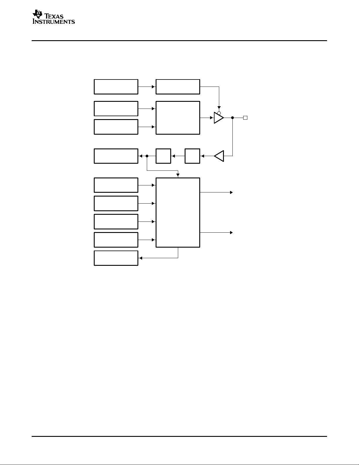
1.3 Functional Block Diagram
DIR
register logic
Direction
register
SET_DATA
CLR_DATA
register
OUTDATA
register
GPIO
signal
Synchronizing flip−flops
INDATA
register
SET_RIS_TRIG
register
CLR_RIS_TRIG
register
SET_FAL_TRIG
register
CLR_FAL_TRIG
register
register
INSTAT
Edge
detection
logic
EDMA event
Interrupt
to ARM
or DSP
CPU
Figure 1 shows a block diagram of the GPIO peripheral.
Peripheral Architecture
Figure 1. GPIO Peripheral Block Diagram
1.4 Industry Standard(s) Compliance Statement
The GPIO peripheral connects to external devices. While it is possible that the software implements some
standard connectivity protocol over GPIO, the GPIO peripheral itself is not compliant with any such
standards.
2 Peripheral Architecture
The following sections describe the GPIO peripheral.
2.1 Clock Control
The input clock to the GPIO peripheral is the SYSCLK5 chip-level clock. SYSCLK5 represents PLL1
divided by 6. The maximum operation speed for the GPIO peripheral is 10 MHz.
2.2 Signal Descriptions
The DM644x device supports up to 71 GPIO signals. GPIO[53:0] are 1.8V I/O signals. GPIOV33_[16:0]
are 3.3V I/O signals. For information on the package pinout of each GPIO signal, refer to the device data
manual.
SPRUE25 – December 2005 General-Purpose Input/Output (GPIO) 9
Page 10

www.ti.com
Peripheral Architecture
2.3 GPIO Register Structure
The GPIO signals are grouped into banks of 16 signals per bank.
The GPIO configuration registers are organized as one 32-bit register per pair of banks. When there are
an odd number of banks, the upper 16-bit of registers for the last pair are reserved and have no effect. For
the interrupt configuration, the registers associated with GPIO signals that do not support interrupt
capability are also reserved and have no effect. Table 1 shows the banks and register control bit
information associated with each GPIO pin on the device. The table can be used to locate the register bits
that control each GPIO signal. For detailed information on the GPIO registers, see section Section 3 .
GPIO Signal Bank Number Register Pair Number Register Field Number Bit Number
Table 1. GPIO Register Bits and Banks Associated With GPIO Pins
GPIO0 0 register_name01 field_name0 Bit 0
GPIO1 0 register_name01 field_name1 Bit 1
GPIO2 0 register_name01 field_name2 Bit 2
GPIO3 0 register_name01 field_name3 Bit 3
GPIO4 0 register_name01 field_name4 Bit 4
GPIO5 0 register_name01 field_name5 Bit 5
GPIO6 0 register_name01 field_name6 Bit 6
GPIO7 0 register_name01 field_name7 Bit 7
GPIO8 0 register_name01 field_name8 Bit 8
GPIO9 0 register_name01 field_name9 Bit 9
GPIO10 0 register_name01 field_name10 Bit 10
GPIO11 0 register_name01 field_name11 Bit 11
GPIO12 0 register_name01 field_name12 Bit 12
GPIO13 0 register_name01 field_name13 Bit 13
GPIO14 0 register_name01 field_name14 Bit 14
GPIO15 0 register_name01 field_name15 Bit 15
GPIO16 1 register_name01 field_name16 Bit 16
GPIO17 1 register_name01 field_name17 Bit 17
GPIO18 1 register_name01 field_name18 Bit 18
GPIO19 1 register_name01 field_name19 Bit 19
GPIO20 1 register_name01 field_name20 Bit 20
GPIO21 1 register_name01 field_name21 Bit 21
GPIO22 1 register_name01 field_name22 Bit 22
GPIO23 1 register_name01 field_name23 Bit 23
GPIO24 1 register_name01 field_name24 Bit 24
GPIO25 1 register_name01 field_name25 Bit 25
GPIO26 1 register_name01 field_name26 Bit 26
GPIO27 1 register_name01 field_name27 Bit 27
GPIO28 1 register_name01 field_name28 Bit 28
GPIO29 1 register_name01 field_name29 Bit 29
GPIO30 1 register_name01 field_name30 Bit 30
GPIO31 1 register_name01 field_name31 Bit 31
GPIO32 2 register_name23 field_name32 Bit 0
GPIO33 2 register_name23 field_name33 Bit 1
GPIO34 2 register_name23 field_name34 Bit 2
GPIO35 2 register_name23 field_name35 Bit 3
GPIO36 2 register_name23 field_name36 Bit 4
GPIO37 2 register_name23 field_name37 Bit 5
General-Purpose Input/Output (GPIO)10 SPRUE25 – December 2005
Page 11

www.ti.com
Peripheral Architecture
Table 1. GPIO Register Bits and Banks Associated With GPIO Pins (continued)
GPIO Signal Bank Number Register Pair Number Register Field Number Bit Number
GPIO38 2 register_name23 field_name38 Bit 6
GPIO39 2 register_name23 field_name39 Bit 7
GPIO40 2 register_name23 field_name40 Bit 8
GPIO41 2 register_name23 field_name41 Bit 9
GPIO42 2 register_name23 field_name42 Bit 10
GPIO43 2 register_name23 field_name43 Bit 11
GPIO44 2 register_name23 field_name44 Bit 12
GPIO45 2 register_name23 field_name45 Bit 13
GPIO46 2 register_name23 field_name46 Bit 14
GPIO47 2 register_name23 field_name47 Bit 15
GPIO48 3 register_name23 field_name48 Bit 16
GPIO49 3 register_name23 field_name49 Bit 17
GPIO50 3 register_name23 field_name50 Bit 18
GPIO51 3 register_name23 field_name51 Bit 19
GPIO52 3 register_name23 field_name52 Bit 20
GPIO53 3 register_name23 field_name53 Bit 21
GPIOV33_0 3 register_name23 field_name54 Bit 22
GPIOV33_1 3 register_name23 field_name55 Bit 23
GPIOV33_2 3 register_name23 field_name56 Bit 24
GPIOV33_3 3 register_name23 field_name57 Bit 25
GPIOV33_4 3 register_name23 field_name58 Bit 26
GPIOV33_5 3 register_name23 field_name59 Bit 27
GPIOV33_6 3 register_name23 field_name60 Bit 28
GPIOV33_7 3 register_name23 field_name61 Bit 29
GPIOV33_8 3 register_name23 field_name62 Bit 30
GPIOV33_9 3 register_name23 field_name63 Bit 31
GPIOV33_10 4 register_name4 field_name64 Bit 0
GPIOV33_11 4 register_name4 field_name65 Bit 1
GPIOV33_12 4 register_name4 field_name66 Bit 2
GPIOV33_13 4 register_name4 field_name67 Bit 3
GPIOV33_14 4 register_name4 field_name68 Bit 4
GPIOV33_15 4 register_name4 field_name69 Bit 5
GPIOV33_16 4 register_name4 field_name70 Bit 6
2.4 Using a GPIO Signal as an Output
GPIO signals are configured to operate as inputs or outputs by writing the appropriate value to the GPIO
direction register (DIR). This section describes using the GPIO signal as an output signal.
2.4.1 Configuring a GPIO Output Signal
To configure a given GPIO signal as an output, clear the bit in DIR that is associated with the desired
GPIO signal. For detailed information on DIR, see Section 3 .
SPRUE25 – December 2005 General-Purpose Input/Output (GPIO) 11
Page 12

www.ti.com
Peripheral Architecture
2.4.2 Controlling the GPIO Output Signal State
There are three registers that control the output state driven on a GPIO signal configured as an output:
• GPIO set data register (SET_DATA) controls driving GPIO signals high
• GPIO clear data register (CLR_DATA) controls driving GPIO signals low
• GPIO output data register (OUT_DATA) contains the current state of the output signals
Reading SET_DATA, CLR_DATA, and OUT_DATA returns the output state not necessarily the actual
signal state (since some signals may be configured as inputs). The actual signal state is read using the
GPIO input data register (IN_DATA) associated with the desired GPIO signal. IN_DATA contains the
actual logic state on the external signal.
For detailed information on these registers, see Section 3 .
2.4.2.1 Driving a GPIO Output Signal High
To drive a GPIO signal high, use one of the following methods:
• Write a logic 1 to the bit in SET_DATA associated with the desired GPIO signal(s) to be driven high.
Bit positions in SET_DATA containing logic 0 do not affect the state of the associated output signals.
• Modify the bit in OUT_DATA associated with the desired GPIO signal by using a read-modify-write
operation. The logic states driven on the GPIO output signals match the logic values written to all bits
in OUT_DATA.
For GPIO signals configured as inputs, the values written to the associated SET_DATA, CLR_DATA, and
OUT_DATA bits have no effect.
2.4.2.2 Driving a GPIO Output Signal Low
To drive a GPIO signal low, use one of the following methods:
• Write a logic 1 to the bit in CLR_DATA associated with the desired GPIO signal(s) to be driven low. Bit
positions in CLR_DATA containing logic 0 do not affect the state of the associated output signals.
• Modify the bit in OUT_DATA associated with the desired GPIO signal by using a read-modify-write
operation. The logic states driven on the GPIO output signals match the logic values written to all bits
in OUT_DATA.
For GPIO signals configured as inputs, the values written to the associated SET_DATA, CLR_DATA, and
OUT_DATA bits have no effect.
2.5 Using a GPIO Signal as an Input
GPIO signals are configured to operate as inputs or outputs by writing the appropriate value to the GPIO
direction register (DIR). This section describes using the GPIO signal as an input signal.
2.5.1 Configuring a GPIO Input Signal
To configure a given GPIO signal as an input, set the bit in DIR that is associated with the desired GPIO
signal. For detailed information on DIR, see Section 3 .
2.5.2 Reading a GPIO Input Signal
The current state of the GPIO signals is read using the GPIO input data register (IN_DATA).
• For GPIO signals configured as inputs, reading IN_DATA returns the state of the input signal
synchronized to the GPIO peripheral clock.
• For GPIO signals configured as outputs, reading IN_DATA returns the output value being driven by the
device.
Some signals may utilize open-drain output buffers for wired-logic operations. For open-drain GPIO
signals, reading IN_DATA returns the wired-logic value on the signal (which will not be driven by the
device alone). Information on any signals using open-drain outputs is available in the device data manual.
To use GPIO input signals as interrupt sources, see section Section 2.7 .
12 General-Purpose Input/Output (GPIO) SPRUE25 – December 2005
Page 13

www.ti.com
2.6 Reset Considerations
The GPIO peripheral has two reset sources: software reset and hardware reset.
2.6.1 Software Reset Considerations
A software reset (such as a reset initiated through the emulator) does not modify the configuration and
state of the GPIO signals.
2.6.2 Hardware Reset Considerations
A hardware reset does reset the GPIO configuration and data registers to their default states; therefore,
affecting the configuration and state of the GPIO signals.
2.7 Interrupt Support
The GPIO peripheral can send an interrupt event to the ARM and/or the DSP.
2.7.1 Interrupt Events and Requests
A subset of the GPIO signals can also be configured to generate interrupts. The DM644x supports
interrupts from single GPIO signals, interrupts from banks of GPIO signals, or both. The interrupt mapping
from the GPIO peripheral to the ARM and DSP CPUs is shown in Table 2 .
Interrupt Source Acronym ARM Interrupt Number DSP Interrupt Number
GPIO0 GPIO0 48 64
GPIO1 GPIO1 49 65
GPIO2 GPIO2 50 66
GPIO3 GPIO3 51 67
GPIO4 GPIO4 52 68
GPIO5 GPIO5 53 69
GPIO6 GPIO6 54 70
GPIO7 GPIO7 55 71
GPIO Bank 0 GPIOBNK0 56 72
GPIO Bank 1 GPIOBNK1 57 73
GPIO Bank 2 GPIOBNK2 58 74
GPIO Bank 3 GPIOBNK3 59 75
GPIO Bank 4 GPIOBNK4 69 76
Peripheral Architecture
Table 2. GPIO Interrupts to the ARM CPU and DSP CPU
2.7.2 Enabling GPIO Interrupt Events
GPIO interrupt events are enabled in banks of 16 by setting the appropriate bit(s) in the GPIO interrupt
per-bank enable register (BINTEN). For example, to enable bank 0 interrupts (events from GPIO[15-0]),
set bit 0 in BINTEN; to enable bank 3 interrupts (events from GPIO[63-48]), set bit 3 in BINTEN.
For detailed information on BINTEN, see Section 3 .
SPRUE25 – December 2005 General-Purpose Input/Output (GPIO) 13
Page 14

www.ti.com
Peripheral Architecture
2.7.3 Configuring GPIO Interrupt Edge Triggering
Each GPIO interrupt source can be configured to generate an interrupt on the GPIO signal rising edge,
falling edge, both edges, or neither edge (no event). The edge detection is synchronized to the GPIO
peripheral module clock.
The following four registers control the configuration of the GPIO interrupt edge detection:
• The GPIO set rising edge interrupt register (SET_RIS_TRIG) enables GPIO interrupts on the
occurrence of a rising edge on the GPIO signal.
• The GPIO clear rising edge interrupt register (CLR_RIS_TRIG) disables GPIO interrupts on the
occurrence of a rising edge on the GPIO signal.
• The GPIO set falling edge interrupt register (SET_FAL_TRIG) enables GPIO interrupts on the
occurrence of a falling edge on the GPIO signal.
• The GPIO clear falling edge interrupt register (CLR_FAL_TRIG) disables GPIO interrupts on the
occurrence of a falling edge on the GPIO signal.
To configure a GPIO interrupt to occur only on rising edges of the GPIO signal:
• Write a logic 1 to the associated bit in SET_RIS_TRIG
To configure a GPIO interrupt to occur only on falling edges of the GPIO signal:
• Write a logic 1 to the associated bit in SET_FAL_TRIG
To configure a GPIO interrupt to occur on both the rising and falling edges of the GPIO signal:
• Write a logic 1 to the associated bit in SET_RIS_TRIG
• Write a logic 1 to the associated bit in SET_FAL_TRIG
To disable a specific GPIO interrupt:
• Write a logic 1 to the associated bit in CLR_RIS_TRIG
• Write a logic 1 to the associated bit in CLR_FAL_TRIG
For detailed information on these registers, see Section 3 .
Note that the direction of the GPIO signal does not have to be an input for the interrupt event generation
to work. When a GPIO signal is configured as an output, the software can change the GPIO signal state
and, in turn, generate an interrupt. This can be useful for debugging interrupt signal connectivity.
2.7.4 GPIO Interrupt Status
The status of GPIO interrupt events can be monitored by reading the GPIO interrupt status register
(INTSTAT). Pending GPIO interrupts are indicated with a logic 1 in the associated bit position; interrupts
that are not pending are indicated with a logic 0.
For individual GPIO interrupts that are directly routed to the ARM or DSP subsystem, the interrupt status
can be read by reading the associated interrupt flag in the CPU. For the GPIO bank interrupts, INTSTAT
can be used to determine which GPIO interrupt occurred. It is the responsibility of software to ensure that
all pending GPIO interrupts are appropriately serviced.
Pending GPIO interrupt flags can be cleared by writing a logic 1 to the associated bit position in INTSTAT.
For detailed information on INTSTAT, see Section 3 .
2.7.5 Interrupt Multiplexing
No GPIO interrupts are multiplexed with other interrupt functions on the DM644x.
14 General-Purpose Input/Output (GPIO) SPRUE25 – December 2005
Page 15

www.ti.com
2.8 EDMA Event Support
The GPIO peripheral can provide synchronization events to the EDMA. The EDMA events supported on
this device are listed in Table 3 .
Peripheral Architecture
Table 3. GPIO Synchronization Events to the EDMA
Interrupt Source EDMA Synchronization Event Number
GPIO0 32
GPIO1 33
GPIO2 34
GPIO3 35
GPIO4 36
GPIO5 37
GPIO6 38
GPIO7 39
GPIO Bank 0 40
GPIO Bank 1 41
GPIO Bank 2 42
GPIO Bank 3 43
GPIO Bank 4 44
2.9 Power Management
2.10 Emulation Considerations
The GPIO peripheral can be placed in reduced-power modes to conserve power during periods of low
activity. The power management of the GPIO peripheral is controlled by the processor Power and Sleep
Controller (PSC). The PSC acts as a master controller for power management for all of the peripherals on
the device. For detailed information on power management procedures using the PSC, see the
TMS320DM644x DMSoC ARM Subsystem Reference Guide (SPRUE14).
When the GPIO peripheral is placed in a low-power state by the PSC, the interrupt generation capability is
suspended until the GPIO peripheral is removed from the low-power state. While in the low-power state,
the GPIO signals configured as outputs are maintained at their state prior to the GPIO peripheral entering
the low-power state.
The GPIO peripheral is not affected by emulation suspend events (such as halts and breakpoints).
SPRUE25 – December 2005 General-Purpose Input/Output (GPIO) 15
Page 16

www.ti.com
Registers
3 Registers
Table 4 lists the memory-mapped registers for the general-purpose input/output (GPIO). See the
device-specific data manual for the memory address of these registers.
Table 4. General-Purpose Input/Output (GPIO) Registers
Offset Acronym Register Description Section
0h PID Peripheral Identification Register Section 3.1
8h BINTEN GPIO Interrupt Per-Bank Enable Register Section 3.2
GPIO Banks 0 and 1
10h DIR01 GPIO Banks 0 and 1 Direction Register Section 3.3
14h OUT_DATA01 GPIO Banks 0 and 1 Output Data Register Section 3.4
18h SET_DATA01 GPIO Banks 0 and 1 Set Data Register Section 3.5
1Ch CLR_DATA01 GPIO Banks 0 and 1 Clear Data Register Section 3.6
20h IN_DATA01 GPIO Banks 0 and 1 Input Data Register Section 3.7
24h SET_RIS_TRIG01 GPIO Banks 0 and 1 Set Rising Edge Interrupt Register Section 3.8
28h CLR_RIS_TRIG01 GPIO Banks 0 and 1 Clear Rising Edge Interrupt Register Section 3.9
2Ch SET_FAL_TRIG01 GPIO Banks 0 and 1 Set Falling Edge Interrupt Register Section 3.10
30h CLR_FAL_TRIG01 GPIO Banks 0 and 1 Clear Falling Edge Interrupt Register Section 3.11
34h INTSTAT01 GPIO Banks 0 and 1 Interrupt Status Register Section 3.12
GPIO Banks 2 and 3
38h DIR23 GPIO Banks 2 and 3 Direction Register Section 3.3
3Ch OUT_DATA23 GPIO Banks 2 and 3 Output Data Register Section 3.4
40h SET_DATA23 GPIO Banks 2 and 3 Set Data Register Section 3.5
44h CLR_DATA23 GPIO Banks 2 and 3 Clear Data Register Section 3.6
48h IN_DATA23 GPIO Banks 2 and 3 Input Data Register Section 3.7
4Ch SET_RIS_TRIG23 GPIO Banks 2 and 3 Set Rising Edge Interrupt Register Section 3.8
50h CLR_RIS_TRIG23 GPIO Banks 2 and 3 Clear Rising Edge Interrupt Register Section 3.9
54h SET_FAL_TRIG23 GPIO Banks 2 and 3 Set Falling Edge Interrupt Register Section 3.10
58h CLR_FAL_TRIG23 GPIO Banks 2 and 3 Clear Falling Edge Interrupt Register Section 3.11
5Ch INTSTAT23 GPIO Banks 2 and 3 Interrupt Status Register Section 3.12
GPIO Bank 4
60h DIR4 GPIO Bank 4 Direction Register Section 3.3
64h OUT_DATA4 GPIO Bank 4 Output Data Register Section 3.4
68h SET_DATA4 GPIO Bank 4 Set Data Register Section 3.5
6Ch CLR_DATA4 GPIO Bank 4 Clear Data Register Section 3.6
70h IN_DATA4 GPIO Bank 4 Input Data Register Section 3.7
74h SET_RIS_TRIG4 GPIO Bank 4 Set Rising Edge Interrupt Register Section 3.8
78h CLR_RIS_TRIG4 GPIO Bank 4 Clear Rising Edge Interrupt Register Section 3.9
7Ch SET_FAL_TRIG4 GPIO Bank 4 Set Falling Edge Interrupt Register Section 3.10
80h CLR_FAL_TRIG4 GPIO Bank 4 Clear Falling Edge Interrupt Register Section 3.11
84h INTSTAT4 GPIO Bank 4 Interrupt Status Register Section 3.12
16 General-Purpose Input/Output (GPIO) SPRUE25 – December 2005
Page 17

www.ti.com
3.1 Peripheral Identification Register (PID)
The peripheral identification register (PID) contains identification data (type, class, and revision) for the
peripheral. PID is shown in Figure 2 and described in Table 5 .
Figure 2. Peripheral Identification Register (PID)
31 24 23 16
Reserved TID
R-0 R-0
15 8 7 0
CID REV
R-0 R-0
LEGEND: R = Read only; - n = value after reset
Table 5. Peripheral Identification Register (PID) Field Descriptions
Bit Field Value Description
31-24 Reserved 0 Reserved
23-16 TID 0-Fh Identifies type of peripheral.
15-8 CID 0-Fh Identifies class of peripheral.
7-0 REV 0-Fh Identifies revision of peripheral.
Registers
SPRUE25 – December 2005 General-Purpose Input/Output (GPIO) 17
Page 18

www.ti.com
Registers
3.2 GPIO Interrupt Per-Bank Enable Register (BINTEN)
The GPIO interrupt per-bank enable register (BINTEN) is shown in Figure 3 and described in Table 6 . For
information on which GPIO signals are associated with each bank, see Table 1 .
Figure 3. GPIO Interrupt Per-Bank Enable Register (BINTEN)
31 16
Reserved
R-0
15 5 4 3 2 1 0
Reserved EN4 EN3 EN2 EN1 EN0
R-0 R/W-0 R/W-0 R/W-0 R/W-0 R/W-0
LEGEND: R/W = Read/Write; R = Read only; - n = value after reset
Table 6. GPIO Interrupt Per-Bank Enable Register (BINTEN) Field Descriptions
Bit Field Value Description
31-5 Reserved 0 Reserved
4 EN4 Bank 4 interrupt enable is used to disable or enable the bank 4 interrupts.
0 Bank 4 interrupts are disabled.
1 Bank 4 interrupts are enabled.
3 EN3 Bank 3 interrupt enable is used to disable or enable the bank 3 interrupts.
0 Bank 3 interrupts are disabled.
1 Bank 3 interrupts are enabled.
2 EN2 Bank 2 interrupt enable is used to disable or enable the bank 2 interrupts.
0 Bank 2 interrupts are disabled.
1 Bank 2 interrupts are enabled.
1 EN1 Bank 1 interrupt enable is used to disable or enable the bank 1 interrupts.
0 Bank 1 interrupts are disabled.
1 Bank 1 interrupts are enabled.
0 EN0 Bank 0 interrupt enable is used to disable or enable the bank 0 interrupts.
0 Bank 0 interrupts are disabled.
1 Bank 0 interrupts are enabled.
General-Purpose Input/Output (GPIO)18 SPRUE25 – December 2005
Page 19

www.ti.com
3.3 GPIO Direction Registers (DIR n)
The GPIO direction register (DIR n) determines if GPIO pin n in GPIO bank I is an input or an output. Each
of the GPIO banks may have up to 16 GPIO pins. By default, all the GPIO pins are configured as inputs
(bit value = 1). The GPIO direction register (DIR01) is shown in Figure 4 , DIR23 is shown in Figure 5 ,
DIR4 is shown in Figure 6 , and described in Table 7 . See Table 1 to determine the DIR n bit associated
with each GPIO bank and pin number.
Figure 4. GPIO Banks 0 and 1 Direction Register (DIR01)
31 30 29 28 27 26 25 24 23 22 21 20 19 18 17 16
DIR31 DIR30 DIR29 DIR28 DIR27 DIR26 DIR25 DIR24 DIR23 DIR22 DIR21 DIR20 DIR19 DIR18 DIR17 DIR16
R/W-1
15 14 13 12 11 10 9 8 7 6 5 4 3 2 1 0
DIR15 DIR14 DIR13 DIR12 DIR11 DIR10 DIR9 DIR8 DIR7 DIR6 DIR5 DIR4 DIR3 DIR2 DIR1 DIR0
R/W-1
LEGEND: R/W = Read/Write; - n = value after reset
Figure 5. GPIO Banks 2 and 3 Direction Register (DIR23)
31 30 29 28 27 26 25 24 23 22 21 20 19 18 17 16
DIR63 DIR62 DIR61 DIR60 DIR59 DIR58 DIR57 DIR56 DIR55 DIR54 DIR53 DIR52 DIR51 DIR50 DIR49 DIR48
R/W-1
15 14 13 12 11 10 9 8 7 6 5 4 3 2 1 0
DIR47 DIR46 DIR45 DIR44 DIR43 DIR42 DIR41 DIR40 DIR39 DIR38 DIR37 DIR36 DIR35 DIR34 DIR33 DIR32
R/W-1
LEGEND: R/W = Read/Write; - n = value after reset
Registers
Figure 6. GPIO Bank 4 Direction Register (DIR4)
31 16
Reserved
R-0
15 7 6 5 4 3 2 1 0
Reserved DIR70 DIR69 DIR68 DIR67 DIR66 DIR65 DIR64
R-0 R/W-1
LEGEND: R/W = Read/Write; R = Read only; - n = value after reset
Table 7. GPIO Direction Register (DIR n) Field Descriptions
Bit Field Value Description
31-16 DIR n Direction of GPIO pin n. The DIR n bit is used to control the direction (output = 0, input = 1) of pin n on
15-0 DIR n Direction of GPIO pin n. The DIR n bit is used to control the direction (output = 0, input = 1) of pin n on
GPIO bank 2 I + 1. This bit field configures the GPIO pins on GPIO banks 1 and 3.
0 GPIO pin n is an output.
1 GPIO pin n is an input.
GPIO bank 2 I. This bit field configures the GPIO pins on GPIO banks 0, 2, and 4.
0 GPIO pin n is an output.
1 GPIO pin n is an input.
SPRUE25 – December 2005 General-Purpose Input/Output (GPIO) 19
Page 20

www.ti.com
Registers
3.4 GPIO Output Data Register (OUT_DATA n)
The GPIO output data register (OUT_DATA n) determines the value driven on the corresponding GPIO pin
n in GPIO bank I, if the pin is configured as an output (DIR n = 0). Writes do not affect pins not configured
as GPIO outputs. The bits in OUT_DATA n are set or cleared by writing directly to this register. A read of
OUT_DATA n returns the value of the register not the value at the pin (that might be configured as an
input). The GPIO output data register (OUT_DATA01) is shown in Figure 7 , OUT_DATA23 is shown in
Figure 8 , OUT_DATA4 is shown in Figure 9 , and described in Table 8 . See Table 1 to determine the
OUT_DATA n bit associated with each GPIO bank and pin number.
Figure 7. GPIO Banks 0 and 1 Output Data Register (OUT_DATA01)
31 30 29 28 27 26 25 24 23 22 21 20 19 18 17 16
OUT31 OUT30 OUT29 OUT28 OUT27 OUT26 OUT25 OUT24 OUT23 OUT22 OUT21 OUT20 OUT19 OUT18 OUT17 OUT16
R/W-0
15 14 13 12 11 10 9 8 7 6 5 4 3 2 1 0
OUT15 OUT14 OUT13 OUT12 OUT11 OUT10 OUT9 OUT8 OUT7 OUT6 OUT5 OUT4 OUT3 OUT2 OUT1 OUT0
R/W-0
LEGEND: R/W = Read/Write; - n = value after reset
Figure 8. GPIO Banks 2 and 3 Output Data Register (OUT_DATA23)
31 30 29 28 27 26 25 24 23 22 21 20 19 18 17 16
OUT63 OUT62 OUT61 OUT60 OUT59 OUT58 OUT57 OUT56 OUT55 OUT54 OUT53 OUT52 OUT51 OUT50 OUT49 OUT48
R/W-0
15 14 13 12 11 10 9 8 7 6 5 4 3 2 1 0
OUT47 OUT46 OUT45 OUT44 OUT43 OUT42 OUT41 OUT40 OUT39 OUT38 OUT37 OUT36 OUT35 OUT34 OUT33 OUT32
R/W-0
LEGEND: R/W = Read/Write; - n = value after reset
Figure 9. GPIO Bank 4 Output Data Register (OUT_DATA4)
31 16
Reserved
R-0
15 7 6 5 4 3 2 1 0
Reserved OUT70 OUT69 OUT68 OUT67 OUT66 OUT65 OUT64
R-0 R/W-0
LEGEND: R/W = Read/Write; R = Read only; - n = value after reset
Table 8. GPIO Output Data Register (OUT_DATA n) Field Descriptions
Bit Field Value Description
31-16 OUT n Output drive state of GPIO pin n. The OUT n bit is used to drive the output (low = 0, high = 1) of pin n on
15-0 OUT n Output drive state of GPIO pin n. The OUT n bit is used to drive the output (low = 0, high = 1) of pin n on
GPIO bank 2 I + 1 only when pin n is configured as an output (DIR n = 0). The OUT n bit is ignored when
GPIO pin n is configured as an input. This bit field configures the GPIO pins on GPIO banks 1 and 3.
0 GPIO pin n is driven low.
1 GPIO pin n is driven high.
GPIO bank 2 I only when pin n is configured as an output (DIR n = 0). The OUT n bit is ignored when GPIO
pin n is configured as an input. This bit field configures the GPIO pins on GPIO banks 0, 2, and 4.
0 GPIO pin n is driven low.
1 GPIO pin n is driven high.
20 General-Purpose Input/Output (GPIO) SPRUE25 – December 2005
Page 21

www.ti.com
3.5 GPIO Set Data Register (SET_DATA n)
The GPIO set data register (SET_DATA n) controls driving high the corresponding GPIO pin n in GPIO
bank I, if the pin is configured as an output (DIR n = 0). Writes do not affect pins not configured as GPIO
outputs. The bits in SET_DATA n are set or cleared by writing directly to this register. A read of the SET n
bit returns the output drive state of the corresponding GPIO pin n. The GPIO set data register
(SET_DATA01) is shown in Figure 10 , SET_DATA23 is shown in Figure 11 , SET_DATA4 is shown in
Figure 12 , and described in Table 9 . See Table 1 to determine the SET_DATA n bit associated with each
GPIO bank and pin number.
Figure 10. GPIO Banks 0 and 1 Set Data Register (SET_DATA01)
31 30 29 28 27 26 25 24 23 22 21 20 19 18 17 16
SET31 SET30 SET29 SET28 SET27 SET26 SET25 SET24 SET23 SET22 SET21 SET20 SET19 SET18 SET17 SET16
R/W-0
15 14 13 12 11 10 9 8 7 6 5 4 3 2 1 0
SET15 SET14 SET13 SET12 SET11 SET10 SET9 SET8 SET7 SET6 SET5 SET4 SET3 SET2 SET1 SET0
R/W-0
LEGEND: R/W = Read/Write; - n = value after reset
Figure 11. GPIO Banks 2 and 3 Set Data Register (SET_DATA23)
31 30 29 28 27 26 25 24 23 22 21 20 19 18 17 16
SET63 SET62 SET61 SET60 SET59 SET58 SET57 SET56 SET55 SET54 SET53 SET52 SET51 SET50 SET49 SET48
R/W-0
15 14 13 12 11 10 9 8 7 6 5 4 3 2 1 0
SET47 SET46 SET45 SET44 SET43 SET42 SET41 SET40 SET39 SET38 SET37 SET36 SET35 SET34 SET33 SET32
R/W-0
LEGEND: R/W = Read/Write; - n = value after reset
Registers
Figure 12. GPIO Bank 4 Set Data Register (SET_DATA4)
31 16
Reserved
R-0
15 7 6 5 4 3 2 1 0
Reserved SET70 SET69 SET68 SET67 SET66 SET65 SET64
R-0 R/W-0
LEGEND: R/W = Read/Write; R = Read only; - n = value after reset
SPRUE25 – December 2005 General-Purpose Input/Output (GPIO) 21
Page 22

www.ti.com
Registers
Table 9. GPIO Set Data Register (SET_DATA n) Field Descriptions
Bit Field Value Description
31-16 SET n Set output drive state of GPIO pin n. The SET n bit is used to set the output of pin n on GPIO bank 2 I + 1
15-0 SET n Set output drive state of GPIO pin n. The SET n bit is used to set the output of pin n on GPIO bank 2 I only
only when pin n is configured as an output (DIR n = 0). The SET n bit is ignored when GPIO pin n is
configured as an input. Writing a 1 to the SET n bit sets the output drive state of the corresponding GPIO
pin n; reading the SET n bit returns the output drive state of the corresponding GPIO pin n. This bit field
configures the GPIO pins on GPIO banks 1 and 3.
0 No effect.
1 Set GPIO pin n output to 1.
when pin n is configured as an output (DIR n = 0). The SET n bit is ignored when GPIO pin n is configured
as an input. Writing a 1 to the SET n bit sets the output drive state of the corresponding GPIO pin n;
reading the SET n bit returns the output drive state of the corresponding GPIO pin n. This bit field
configures the GPIO pins on GPIO banks 0, 2, and 4.
0 No effect.
1 Set GPIO pin n output to 1.
General-Purpose Input/Output (GPIO)22 SPRUE25 – December 2005
Page 23

www.ti.com
3.6 GPIO Clear Data Register (CLR_DATA n)
The GPIO clear data register (CLR_DATA n) controls driving low the corresponding GPIO pin n in GPIO
bank I, if the pin is configured as an output (DIR n = 0). Writes do not affect pins not configured as GPIO
outputs. The bits in CLR_DATA n are set or cleared by writing directly to this register. A read of the CLR n
bit returns the output drive state of the corresponding GPIO pin n. The GPIO clear data register
(CLR_DATA01) is shown in Figure 13 , CLR_DATA23 is shown in Figure 14 , CLR_DATA4 is shown in
Figure 15 , and described in Table 10 . See Table 1 to determine the CLR_DATA n bit associated with each
GPIO bank and pin number.
Figure 13. GPIO Banks 0 and 1 Clear Data Register (CLR_DATA01)
31 30 29 28 27 26 25 24 23 22 21 20 19 18 17 16
CLR31 CLR30 CLR29 CLR28 CLR27 CLR26 CLR25 CLR24 CLR23 CLR22 CLR21 CLR20 CLR19 CLR18 CLR17 CLR16
R/W-0
15 14 13 12 11 10 9 8 7 6 5 4 3 2 1 0
CLR15 CLR14 CLR13 CLR12 CLR11 CLR10 CLR9 CLR8 CLR7 CLR6 CLR5 CLR4 CLR3 CLR2 CLR1 CLR0
R/W-0
LEGEND: R/W = Read/Write; - n = value after reset
Figure 14. GPIO Banks 2 and 3 Clear Data Register (CLR_DATA23)
31 30 29 28 27 26 25 24 23 22 21 20 19 18 17 16
CLR63 CLR62 CLR61 CLR60 CLR59 CLR58 CLR57 CLR56 CLR55 CLR54 CLR53 CLR52 CLR51 CLR50 CLR49 CLR48
R/W-0
15 14 13 12 11 10 9 8 7 6 5 4 3 2 1 0
CLR47 CLR46 CLR45 CLR44 CLR43 CLR42 CLR41 CLR40 CLR39 CLR38 CLR37 CLR36 CLR35 CLR34 CLR33 CLR32
R/W-0
LEGEND: R/W = Read/Write; - n = value after reset
Registers
Figure 15. GPIO Bank 4 Clear Data Register (CLR_DATA4)
31 16
Reserved
R-0
15 7 6 5 4 3 2 1 0
Reserved CLR70 CLR69 CLR68 CLR67 CLR66 CLR65 CLR64
R-0 R/W-0
LEGEND: R/W = Read/Write; R = Read only; - n = value after reset
SPRUE25 – December 2005 General-Purpose Input/Output (GPIO) 23
Page 24

www.ti.com
Registers
Table 10. GPIO Clear Data Register (CLR_DATA n) Field Descriptions
Bit Field Value Description
31-16 CLR n Clear output drive state of GPIO pin n. The CLR n bit is used to clear the output of pin n on GPIO bank
15-0 CLR n Clear output drive state of GPIO pin n. The CLR n bit is used to clear the output of pin n on GPIO bank 2 I
2/ + 1 only when pin n is configured as an output (DIR n = 0). The CLR n bit is ignored when GPIO pin n is
configured as an input. Writing a 1 to the CLR n bit clears the output drive state of the corresponding GPIO
pin n; reading the CLR n bit returns the output drive state of the corresponding GPIO pin n. This bit field
configures the GPIO pins on GPIO banks 1 and 3.
0 No effect.
1 Clear GPIO pin n output to 0.
only when pin n is configured as an output (DIR n = 0). The CLR n bit is ignored when GPIO pin n is
configured as an input. Writing a 1 to the CLR n bit clears the output drive state of the corresponding GPIO
pin n; reading the CLR n bit returns the output drive state of the corresponding GPIO pin n. This bit field
configures the GPIO pins on GPIO banks 0, 2, and 4.
0 No effect.
1 Clear GPIO pin n output to 0.
General-Purpose Input/Output (GPIO)24 SPRUE25 – December 2005
Page 25

www.ti.com
3.7 GPIO Input Data Register (IN_DATA n)
The current state of the GPIO signals is read using the GPIO input data register (IN_DATA n).
• For GPIO signals configured as inputs, reading IN_DATA n returns the state of the input signal
synchronized to the GPIO peripheral clock.
• For GPIO signals configured as outputs, reading IN_DATA n returns the output value being driven by
the device.
The GPIO input data register (IN_DATA01) is shown in Figure 16 , IN_DATA23 is shown in Figure 17 ,
IN_DATA4 is shown in Figure 18 , and described in Table 11 . See Table 1 to determine the IN_DATA n bit
associated with each GPIO bank and pin number.
Figure 16. GPIO Banks 0 and 1 Input Data Register (IN_DATA01)
31 30 29 28 27 26 25 24 23 22 21 20 19 18 17 16
IN31 IN30 IN29 IN28 IN27 IN26 IN25 IN24 IN23 IN22 IN21 IN20 IN19 IN18 IN17 IN16
R-0
15 14 13 12 11 10 9 8 7 6 5 4 3 2 1 0
IN15 IN14 IN13 IN12 IN11 IN10 IN9 IN8 IN7 IN6 IN5 IN4 IN3 IN2 IN1 IN0
R-0
LEGEND: R = Read only; - n = value after reset
Figure 17. GPIO Banks 2 and 3 Input Data Register (IN_DATA23)
31 30 29 28 27 26 25 24 23 22 21 20 19 18 17 16
IN63 IN62 IN61 IN60 IN59 IN58 IN57 IN56 IN55 IN54 IN53 IN52 IN51 IN50 IN49 IN48
R-0
15 14 13 12 11 10 9 8 7 6 5 4 3 2 1 0
IN47 IN46 IN45 IN44 IN43 IN42 IN41 IN40 IN39 IN38 IN37 IN36 IN35 IN34 IN33 IN32
R-0
LEGEND: R = Read only; - n = value after reset
Registers
Figure 18. GPIO Bank 4 Input Data Register (IN_DATA4)
31 16
Reserved
R-0
15 7 6 5 4 3 2 1 0
Reserved IN70 IN69 IN68 IN67 IN66 IN65 IN64
R-0 R-0
LEGEND: R = Read only; - n = value after reset
Table 11. GPIO Input Data Register (IN_DATA n) Field Descriptions
Bit Field Value Description
31-16 IN n Status of GPIO pin n. Reading the IN n bit returns the state of pin n on GPIO bank 2 I + 1. This bit field
15-0 IN n Status of GPIO pin n. Reading the IN n bit returns the state of pin n on GPIO bank 2 I. This bit field returns
returns the status of the GPIO pins on GPIO banks 1 and 3.
0 GPIO pin n is logic low.
1 GPIO pin n is logic high.
the status of the GPIO pins on GPIO banks 0, 2 and 4.
0 GPIO pin n is logic low.
1 GPIO pin n is logic high.
SPRUE25 – December 2005 General-Purpose Input/Output (GPIO) 25
Page 26

www.ti.com
Registers
3.8 GPIO Set Rising Edge Interrupt Register (SET_RIS_TRIG n)
The GPIO set rising edge interrupt register (SET_RIS_TRIG n) enables a rising edge on the GPIO pin to
generate a GPIO interrupt. The GPIO set rising edge interrupt register (SET_RIS_TRIG01) is shown in
Figure 19 , SET_RIS_TRIG23 is shown in Figure 20 , SET_RIS_TRIG4 is shown in Figure 21 , and
described in Table 12 . See Table 1 to determine the SET_RIS_TRIG n bit associated with each GPIO
bank and pin number.
Figure 19. GPIO Banks 0 and 1 Set Rising Edge Interrupt Register (SET_RIS_TRIG01)
31 30 29 28 27 26 25 24
SETRIS31 SETRIS30 SETRIS29 SETRIS28 SETRIS27 SETRIS26 SETRIS25 SETRIS24
R/W-0 R/W-0 R/W-0 R/W-0 R/W-0 R/W-0 R/W-0 R/W-0
23 22 21 20 19 18 17 16
SETRIS23 SETRIS22 SETRIS21 SETRIS20 SETRIS19 SETRIS18 SETRIS17 SETRIS16
R/W-0 R/W-0 R/W-0 R/W-0 R/W-0 R/W-0 R/W-0 R/W-0
15 14 13 12 11 10 9 8
SETRIS15 SETRIS14 SETRIS13 SETRIS12 SETRIS11 SETRIS10 SETRIS9 SETRIS8
R/W-0 R/W-0 R/W-0 R/W-0 R/W-0 R/W-0 R/W-0 R/W-0
7 6 5 4 3 2 1 0
SETRIS7 SETRIS6 SETRIS5 SETRIS4 SETRIS3 SETRIS2 SETRIS1 SETRIS0
R/W-0 R/W-0 R/W-0 R/W-0 R/W-0 R/W-0 R/W-0 R/W-0
LEGEND: R/W = Read/Write; - n = value after reset
Figure 20. GPIO Banks 2 and 3 Set Rising Edge Interrupt Register (SET_RIS_TRIG23)
31 30 29 28 27 26 25 24
SETRIS63 SETRIS62 SETRIS61 SETRIS60 SETRIS59 SETRIS58 SETRIS57 SETRIS56
R/W-0 R/W-0 R/W-0 R/W-0 R/W-0 R/W-0 R/W-0 R/W-0
23 22 21 20 19 18 17 16
SETRIS55 SETRIS54 SETRIS53 SETRIS52 SETRIS51 SETRIS50 SETRIS49 SETRIS48
R/W-0 R/W-0 R/W-0 R/W-0 R/W-0 R/W-0 R/W-0 R/W-0
15 14 13 12 11 10 9 8
SETRIS47 SETRIS46 SETRIS45 SETRIS44 SETRIS43 SETRIS42 SETRIS41 SETRIS40
R/W-0 R/W-0 R/W-0 R/W-0 R/W-0 R/W-0 R/W-0 R/W-0
7 6 5 4 3 2 1 0
SETRIS39 SETRIS38 SETRIS37 SETRIS36 SETRIS35 SETRIS34 SETRIS33 SETRIS32
R/W-0 R/W-0 R/W-0 R/W-0 R/W-0 R/W-0 R/W-0 R/W-0
LEGEND: R/W = Read/Write; - n = value after reset
26 General-Purpose Input/Output (GPIO) SPRUE25 – December 2005
Page 27

www.ti.com
Registers
Figure 21. GPIO Bank 4 Set Rising Edge Interrupt Register (SET_RIS_TRIG4)
31 16
Reserved
R-0
15 8
Reserved
R-0
7 6 5 4 3 2 1 0
Reserved SETRIS70 SETRIS69 SETRIS68 SETRIS67 SETRIS66 SETRIS65 SETRIS64
R-0 R/W-0 R/W-0 R/W-0 R/W-0 R/W-0 R/W-0 R/W-0
LEGEND: R/W = Read/Write; R = Read only; - n = value after reset
Table 12. GPIO Set Rising Edge Interrupt Register (SET_RIS_TRIG n) Field Descriptions
Bit Field Value Description
31-16 SETRIS n Enable rising edge interrupt detection on GPIO pin n. Reading the SETRIS n bit returns the state of
15-0 SETRIS n Enable rising edge interrupt detection on GPIO pin n. Reading the SETRIS n bit returns the state of
pin n on GPIO bank 2 I + 1. This bit field configures the GPIO pins on GPIO banks 1 and 3.
0 No effect.
1 Interrupt is caused by a low-to-high transition on GPIO pin n.
pin n on GPIO bank 2 I. This bit field configures the GPIO pins on GPIO banks 0, 2, and 4.
0 No effect.
1 Interrupt is caused by a low-to-high transition on GPIO pin n.
SPRUE25 – December 2005 General-Purpose Input/Output (GPIO) 27
Page 28

www.ti.com
Registers
3.9 GPIO Clear Rising Edge Interrupt Register (CLR_RIS_TRIG n)
The GPIO clear rising edge interrupt register (CLR_RIS_TRIG n) disables a rising edge on the GPIO pin
from generating a GPIO interrupt. The GPIO clear rising edge interrupt register (CLR_RIS_TRIG01) is
shown in Figure 22 , CLR_RIS_TRIG23 is shown in Figure 23 , CLR_RIS_TRIG4 is shown in Figure 24 ,
and described in Table 13 . See Table 1 to determine the CLR_RIS_TRIG n bit associated with each GPIO
bank and pin number.
Figure 22. GPIO Banks 0 and 1 Clear Rising Edge Interrupt Register (CLR_RIS_TRIG01)
31 30 29 28 27 26 25 24
CLRRIS31 CLRRIS30 CLRRIS29 CLRRIS28 CLRRIS27 CLRRIS26 CLRRIS25 CLRRIS24
R/W-0 R/W-0 R/W-0 R/W-0 R/W-0 R/W-0 R/W-0 R/W-0
23 22 21 20 19 18 17 16
CLRRIS23 CLRRIS22 CLRRIS21 CLRRIS20 CLRRIS19 CLRRIS18 CLRRIS17 CLRRIS16
R/W-0 R/W-0 R/W-0 R/W-0 R/W-0 R/W-0 R/W-0 R/W-0
15 14 13 12 11 10 9 8
CLRRIS15 CLRRIS14 CLRRIS13 CLRRIS12 CLRRIS11 CLRRIS10 CLRRIS9 CLRRIS8
R/W-0 R/W-0 R/W-0 R/W-0 R/W-0 R/W-0 R/W-0 R/W-0
7 6 5 4 3 2 1 0
CLRRIS7 CLRRIS6 CLRRIS5 CLRRIS4 CLRRIS3 CLRRIS2 CLRRIS1 CLRRIS0
R/W-0 R/W-0 R/W-0 R/W-0 R/W-0 R/W-0 R/W-0 R/W-0
LEGEND: R/W = Read/Write; - n = value after reset
Figure 23. GPIO Banks 2 and 3 Clear Rising Edge Interrupt Register (CLR_RIS_TRIG23)
31 30 29 28 27 26 25 24
CLRRIS63 CLRRIS62 CLRRIS61 CLRRIS60 CLRRIS59 CLRRIS58 CLRRIS57 CLRRIS56
R/W-10 R/W-0 R/W-0 R/W-0 R/W-0 R/W-0 R/W-0 R/W-0
23 22 21 20 19 18 17 16
CLRRIS55 CLRRIS54 CLRRIS53 CLRRIS52 CLRRIS51 CLRRIS50 CLRRIS49 CLRRIS48
R/W-0 R/W-0 R/W-0 R/W-0 R/W-0 R/W-0 R/W-0 R/W-0
15 14 13 12 11 10 9 8
CLRRIS47 CLRRIS46 CLRRIS45 CLRRIS44 CLRRIS43 CLRRIS42 CLRRIS41 CLRRIS40
R/W-0 R/W-0 R/W-0 R/W-0 R/W-0 R/W-0 R/W-0 R/W-0
7 6 5 4 3 2 1 0
CLRRIS39 CLRRIS38 CLRRIS37 CLRRIS36 CLRRIS35 CLRRIS34 CLRRIS33 CLRRIS32
R/W-0 R/W-0 R/W-0 R/W-0 R/W-0 R/W-0 R/W-0 R/W-0
LEGEND: R/W = Read/Write; - n = value after reset
28 General-Purpose Input/Output (GPIO) SPRUE25 – December 2005
Page 29

www.ti.com
Figure 24. GPIO Bank 4 Clear Rising Edge Interrupt Register (CLR_RIS_TRIG4)
31 16
Reserved
R-0
15 8
Reserved
R-0
7 6 5 4 3 2 1 0
Reserved CLRRIS70 CLRRIS69 CLRRIS68 CLRRIS67 CLRRIS66 CLRRIS65 CLRRIS64
R-0 R/W-0 R/W-0 R/W-0 R/W-0 R/W-0 R/W-0 R/W-0
LEGEND: R/W = Read/Write; R = Read only; - n = value after reset
Table 13. GPIO Clear Rising Edge Interrupt Register (CLR_RIS_TRIG n) Field Descriptions
Bit Field Value Description
31-16 CLRRIS n Disable rising edge interrupt detection on GPIO pin n. Reading the CLRRIS n bit returns the
complement state of pin n on GPIO bank 2 I + 1. This bit field configures the GPIO pins on GPIO
banks 1 and 3.
0 No effect.
1 No interrupt is caused by a low-to-high transition on GPIO pin n.
15-0 CLRRIS n Disable rising edge interrupt detection on GPIO pin n. Reading the CLRRIS n bit returns the
complement state of pin n on GPIO bank 2 I. This bit field configures the GPIO pins on GPIO banks
0, 2, and 4.
0 No effect.
1 No interrupt is caused by a low-to-high transition on GPIO pin n.
Registers
SPRUE25 – December 2005 General-Purpose Input/Output (GPIO) 29
Page 30

www.ti.com
Registers
3.10 GPIO Set Falling Edge Interrupt Register (SET_FAL_TRIG n)
The GPIO set falling edge interrupt register (SET_FAL_TRIG n) enables a falling edge on the GPIO pin to
generate a GPIO interrupt. The GPIO set falling edge interrupt register (SET_FAL_TRIG01) is shown in
Figure 25 , SET_FAL_TRIG23 is shown in Figure 26 , SET_FAL_TRIG4 is shown in Figure 27 , and
described in Table 14 . See Table 1 to determine the SET_FAL_TRIG n bit associated with each GPIO
bank and pin number.
Figure 25. GPIO Banks 0 and 1 Set Falling Edge Interrupt Register (SET_FAL_TRIG01)
31 30 29 28 27 26 25 24
SETFAL31 SETFAL30 SETFAL29 SETFAL28 SETFAL27 SETFAL26 SETFAL25 SETFAL24
R/W-0 R/W-0 R/W-0 R/W-0 R/W-0 R/W-0 R/W-0 R/W-0
23 22 21 20 19 18 17 16
SETFAL23 SETFAL22 SETFAL21 SETFAL20 SETFAL19 SETFAL18 SETFAL17 SETFAL16
R/W-0 R/W-0 R/W-0 R/W-0 R/W-0 R/W-0 R/W-0 R/W-0
15 14 13 12 11 10 9 8
SETFAL15 SETFAL14 SETFAL13 SETFAL12 SETFAL11 SETFAL10 SETFAL9 SETFAL8
R/W-0 R/W-0 R/W-0 R/W-0 R/W-0 R/W-0 R/W-0 R/W-0
7 6 5 4 3 2 1 0
SETFAL7 SETFAL6 SETFAL5 SETFAL4 SETFAL3 SETFAL2 SETFAL1 SETFAL0
R/W-0 R/W-0 R/W-0 R/W-0 R/W-0 R/W-0 R/W-0 R/W-0
LEGEND: R/W = Read/Write; - n = value after reset
Figure 26. GPIO Banks 2 and 3 Set Falling Edge Interrupt Register (SET_FAL_TRIG23)
31 30 29 28 27 26 25 24
SETFAL63 SETFAL62 SETFAL61 SETFAL60 SETFAL59 SETFAL58 SETFAL57 SETFAL56
R/W-0 R/W-0 R/W-0 R/W-0 R/W-0 R/W-0 R/W-0 R/W-0
23 22 21 20 19 18 17 16
SETFAL55 SETFAL54 SETFAL53 SETFAL52 SETFAL51 SETFAL50 SETFAL49 SETFAL48
R/W-0 R/W-0 R/W-0 R/W-0 R/W-0 R/W-0 R/W-0 R/W-0
15 14 13 12 11 10 9 8
SETFAL47 SETFAL46 SETFAL45 SETFAL44 SETFAL43 SETFAL42 SETFAL41 SETFAL40
R/W-0 R/W-0 R/W-0 R/W-0 R/W-0 R/W-0 R/W-0 R/W-0
7 6 5 4 3 2 1 0
SETFAL39 SETFAL38 SETFAL37 SETFAL36 SETFAL35 SETFAL34 SETFAL33 SETFAL32
R/W-0 R/W-0 R/W-0 R/W-0 R/W-0 R/W-0 R/W-0 R/W-0
LEGEND: R/W = Read/Write; - n = value after reset
30 General-Purpose Input/Output (GPIO) SPRUE25 – December 2005
Page 31

www.ti.com
Registers
Figure 27. GPIO Bank 4 Set Falling Edge Interrupt Register (SET_FAL_TRIG4)
31 16
Reserved
R-0
15 8
Reserved
R-0
7 6 5 4 3 2 1 0
Reserved SETFAL70 SETFAL69 SETFAL68 SETFAL67 SETFAL66 SETFAL65 SETFAL64
R-0 R/W-0 R/W-0 R/W-0 R/W-0 R/W-0 R/W-0 R/W-0
LEGEND: R/W = Read/Write; R = Read only; - n = value after reset
Table 14. GPIO Set Falling Edge Interrupt Register (SET_FAL_TRIG n) Field Descriptions
Bit Field Value Description
31-16 SETFAL n Enable falling edge interrupt detection on GPIO pin n. Reading the SETFAL n bit returns the state of
15-0 SETFAL n Enable falling edge interrupt detection on GPIO pin n. Reading the SETFAL n bit returns the state of
pin n on GPIO bank 2 I + 1. This bit field configures the GPIO pins on GPIO banks 1 and 3.
0 No effect.
1 Interrupt is caused by a high-to-low transition on GPIO pin n.
pin n on GPIO bank 2 I. This bit field configures the GPIO pins on GPIO banks 0, 2, and 4.
0 No effect.
1 Interrupt is caused by a high-to-low transition on GPIO pin n.
SPRUE25 – December 2005 General-Purpose Input/Output (GPIO) 31
Page 32

www.ti.com
Registers
3.11 GPIO Clear Falling Edge Interrupt Register (CLR_FAL_TRIG n)
The GPIO clear falling edge interrupt register (CLR_FAL_TRIG n) disables a falling edge on the GPIO pin
from generating a GPIO interrupt. The GPIO clear falling edge interrupt register (CLR_FAL_TRIG01) is
shown in Figure 28 , CLR_FAL_TRIG23 is shown in Figure 29 , CLR_FAL_TRIG4 is shown in Figure 30 ,
and described in Table 15 . See Table 1 to determine the CLR_FAL_TRIG n bit associated with each GPIO
bank and pin number.
Figure 28. GPIO Banks 0 and 1 Clear Falling Edge Interrupt Register (CLR_FAL_TRIG01)
31 30 29 28 27 26 25 24
CLRFAL31 CLRFAL30 CLRFAL29 CLRFAL28 CLRFAL27 CLRFAL26 CLRFAL25 CLRFAL24
R/W-0 R/W-0 R/W-0 R/W-0 R/W-0 R/W-0 R/W-0 R/W-0
23 22 21 20 19 18 17 16
CLRFAL23 CLRFAL22 CLRFAL21 CLRFAL20 CLRFAL19 CLRFAL18 CLRFAL17 CLRFAL16
R/W-0 R/W-0 R/W-0 R/W-0 R/W-0 R/W-0 R/W-0 R/W-0
15 14 13 12 11 10 9 8
CLRFAL15 CLRFAL14 CLRFAL13 CLRFAL12 CLRFAL11 CLRFAL10 CLRFAL9 CLRFAL8
R/W-0 R/W-0 R/W-0 R/W-0 R/W-0 R/W-0 R/W-0 R/W-0
7 6 5 4 3 2 1 0
CLRFAL7 CLRFAL6 CLRFAL5 CLRFAL4 CLRFAL3 CLRFAL2 CLRFAL1 CLRFAL0
R/W-0 R/W-0 R/W-0 R/W-0 R/W-0 R/W-0 R/W-0 R/W-0
LEGEND: R/W = Read/Write; - n = value after reset
Figure 29. GPIO Banks 2 and 3 Clear Falling Edge Interrupt Register (CLR_FAL_TRIG23)
31 30 29 28 27 26 25 24
CLRFAL63 CLRFAL62 CLRFAL61 CLRFAL60 CLRFAL59 CLRFAL58 CLRFAL57 CLRFAL56
R/W-0 R/W-0 R/W-0 R/W-0 R/W-0 R/W-0 R/W-0 R/W-0
23 22 21 20 19 18 17 16
CLRFAL55 CLRFAL54 CLRFAL53 CLRFAL52 CLRFAL51 CLRFAL50 CLRFAL49 CLRFAL48
R/W-0 R/W-0 R/W-0 R/W-0 R/W-0 R/W-0 R/W-0 R/W-0
15 14 13 12 11 10 9 8
CLRFAL47 CLRFAL46 CLRFAL45 CLRFAL44 CLRFAL43 CLRFAL42 CLRFAL41 CLRFAL40
R/W-0 R/W-0 R/W-0 R/W-0 R/W-0 R/W-0 R/W-0 R/W-0
7 6 5 4 3 2 1 0
CLRFAL39 CLRFAL38 CLRFAL37 CLRFAL36 CLRFAL35 CLRFAL34 CLRFAL33 CLRFAL32
R/W-0 R/W-0 R/W-0 R/W-0 R/W-0 R/W-0 R/W-0 R/W-0
LEGEND: R/W = Read/Write; - n = value after reset
32 General-Purpose Input/Output (GPIO) SPRUE25 – December 2005
Page 33

www.ti.com
Figure 30. GPIO Bank 4 Clear Falling Edge Interrupt Register (CLR_FAL_TRIG4)
31 16
Reserved
R-0
15 8
Reserved
R-0
7 6 5 4 3 2 1 0
Reserved CLRFAL70 CLRFAL69 CLRFAL68 CLRFAL67 CLRFAL66 CLRFAL65 CLRFAL64
R-0 R/W-0 R/W-0 R/W-0 R/W-0 R/W-0 R/W-0 R/W-0
LEGEND: R/W = Read/Write; R = Read only; - n = value after reset
Table 15. GPIO Clear Falling Edge Interrupt Register (CLR_FAL_TRIG n) Field Descriptions
Bit Field Value Description
31-16 CLRFAL n Disable falling edge interrupt detection on GPIO pin n. Reading the CLRFAL n bit returns the
complement state of pin n on GPIO bank 2 I + 1. This bit field configures the GPIO pins on GPIO
banks 1 and 3.
0 No effect.
1 No interrupt is caused by a high-to-low transition on GPIO pin n.
15-0 CLRFAL n Disable falling edge interrupt detection on GPIO pin n. Reading the CLRFAL n bit returns the
complement state of pin n on GPIO bank 2 I. This bit field configures the GPIO pins on GPIO banks
0, 2, and 4.
0 No effect.
1 No interrupt is caused by a high-to-low transition on GPIO pin n.
Registers
SPRUE25 – December 2005 General-Purpose Input/Output (GPIO) 33
Page 34

www.ti.com
Registers
3.12 GPIO Interrupt Status Register (INTSTAT n)
The status of GPIO interrupt events can be monitored by reading the GPIO interrupt status register
(INTSTAT n). In the associated bit position, pending GPIO interrupts are indicated with a logic 1 and GPIO
interrupts that are not pending are indicated with a logic 0. The GPIO interrupt status register
(INTSTAT01) is shown in Figure 31 , INTSTAT23 is shown in Figure 32 , INTSTAT4 is shown in Figure 33 ,
and described in Table 16 . See Table 1 to determine the INTSTAT n bit associated with each GPIO bank
and pin number.
Figure 31. GPIO Banks 0 and 1 Interrupt Status Register (INTSTAT01)
31 30 29 28 27 26 25 24
STAT31 STAT30 STAT29 STAT28 STAT27 STAT26 STAT25 STAT24
R/W1C-0 R/W1C-0 R/W1C-0 R/W1C-0 R/W1C-0 R/W1C-0 R/W1C-0 R/W1C-0
23 22 21 20 19 18 17 16
STAT23 STAT22 STAT21 STAT20 STAT19 STAT18 STAT17 STAT16
R/W1C-0 R/W1C-0 R/W1C-0 R/W1C-0 R/W1C-0 R/W1C-0 R/W1C-0 R/W1C-0
15 14 13 12 11 10 9 8
STAT15 STAT14 STAT13 STAT12 STAT11 STAT10 STAT9 STAT8
R/W1C-0 R/W1C-0 R/W1C-0 R/W1C-0 R/W1C-0 R/W1C-0 R/W1C-0 R/W1C-0
7 6 5 4 3 2 1 0
STAT7 STAT6 STATSTAT5 STAT4 STAT3 STAT2 STAT1 STAT0
R/W1C-0 R/W1C-0 R/W1C-0 R/W1C-0 R/W1C-0 R/W1C-0 R/W1C-0 R/W1C-0
LEGEND: R/W = Read/Write; W1C = Write 1 to clear bit (writing 0 has no effect); - n = value after reset
Figure 32. GPIO Banks 2 and 3 Interrupt Status Register (INTSTAT23)
31 30 29 28 27 26 25 24
STAT63 STAT62 STAT61 STAT60 STAT59 STAT58 STAT57 STAT56
R/W1C-0 R/W1C-0 R/W1C-0 R/W1C-0 R/W1C-0 R/W1C-0 R/W1C-0 R/W1C-0
23 22 21 20 19 18 17 16
STAT55 STAT54 STAT53 STAT52 STAT51 STAT50 STAT49 STAT48
R/W1C-0 R/W1C-0 R/W1C-0 R/W1C-0 R/W1C-0 R/W1C-0 R/W1C-0 R/W1C-0
15 14 13 12 11 10 9 8
STAT47 STAT46 STATSTAT45 STAT44 STAT43 STAT42 STAT41 STAT40
R/W1C-0 R/W1C-0 R/W1C-0 R/W1C-0 R/W1C-0 R/W1C-0 R/W1C-0 R/W1C-0
7 6 5 4 3 2 1 0
STAT39 STAT38 STAT37 STAT36 STAT35 STAT34 STAT33 STAT32
R/W1C-0 R/W1C-0 R/W1C-0 R/W1C-0 R/W1C-0 R/W1C-0 R/W1C-0 R/W1C-0
LEGEND: R/W = Read/Write; W1C = Write 1 to clear bit (writing 0 has no effect); - n = value after reset
34 General-Purpose Input/Output (GPIO) SPRUE25 – December 2005
Page 35

www.ti.com
Figure 33. GPIO Bank 4 Interrupt Status Register (INTSTAT4)
31 16
Reserved
R-0
15 8
Reserved
R-0
7 6 5 4 3 2 1 0
Reserved STAT70 STAT69 STAT68 STAT67 STAT66 STAT65 STAT64
R-0 R/W1C-0 R/W1C-0 R/W1C-0 R/W1C-0 R/W1C-0 R/W1C-0 R/W1C-0
LEGEND: R/W = Read/Write; R = Read only; W1C = Write 1 to clear bit (writing 0 has no effect); - n = value after reset
Table 16. GPIO Interrupt Status Register (INTSTAT n) Field Descriptions
Bit Field Value Description
31-16 STAT n Interrupt status of GPIO pin n. The STAT n bit is used to monitor pending GPIO interrupts on pin n of
GPIO bank 2 I + 1. This bit field returns the status of GPIO pins on GPIO banks 1 and 3. Write a 1 to the
STAT n bit to clear the STAT n bit; a write of 0 has no effect.
0 No pending interrupt on GPIO pin n.
1 Pending interrupt on GPIO pin n.
15-0 STAT n Interrupt status of GPIO pin n. The STAT n bit is used to monitor pending GPIO interrupts on pin n of
GPIO bank 2 I. This bit field returns the status of GPIO pins on GPIO banks 0, 2, and 4. Write a 1 to the
STAT n bit to clear the STAT n bit; a write of 0 has no effect.
0 No pending interrupt on GPIO pin n.
1 Pending interrupt on GPIO pin n.
Registers
SPRUE25 – December 2005 General-Purpose Input/Output (GPIO) 35
Page 36

IMPORTANT NOTICE
Texas Instruments Incorporated and its subsidiaries (TI) reserve the right to make corrections, modifications,
enhancements, improvements, and other changes to its products and services at any time and to discontinue
any product or service without notice. Customers should obtain the latest relevant information before placing
orders and should verify that such information is current and complete. All products are sold subject to TI’s terms
and conditions of sale supplied at the time of order acknowledgment.
TI warrants performance of its hardware products to the specifications applicable at the time of sale in
accordance with TI’s standard warranty. Testing and other quality control techniques are used to the extent TI
deems necessary to support this warranty . Except where mandated by government requirements, testing of all
parameters of each product is not necessarily performed.
TI assumes no liability for applications assistance or customer product design. Customers are responsible for
their products and applications using TI components. To minimize the risks associated with customer products
and applications, customers should provide adequate design and operating safeguards.
TI does not warrant or represent that any license, either express or implied, is granted under any TI patent right,
copyright, mask work right, or other TI intellectual property right relating to any combination, machine, or process
in which TI products or services are used. Information published by TI regarding third-party products or services
does not constitute a license from TI to use such products or services or a warranty or endorsement thereof.
Use of such information may require a license from a third party under the patents or other intellectual property
of the third party, or a license from TI under the patents or other intellectual property of TI.
Reproduction of information in TI data books or data sheets is permissible only if reproduction is without
alteration and is accompanied by all associated warranties, conditions, limitations, and notices. Reproduction
of this information with alteration is an unfair and deceptive business practice. TI is not responsible or liable for
such altered documentation.
Resale of TI products or services with statements different from or beyond the parameters stated by TI for that
product or service voids all express and any implied warranties for the associated TI product or service and
is an unfair and deceptive business practice. TI is not responsible or liable for any such statements.
Following are URLs where you can obtain information on other Texas Instruments products and application
solutions:
Products Applications
Amplifiers amplifier.ti.com Audio www.ti.com/audio
Data Converters dataconverter.ti.com Automotive www.ti.com/automotive
DSP dsp.ti.com Broadband www.ti.com/broadband
Interface interface.ti.com Digital Control www.ti.com/digitalcontrol
Logic logic.ti.com Military www.ti.com/military
Power Mgmt power.ti.com Optical Networking www.ti.com/opticalnetwork
Microcontrollers microcontroller.ti.com Security www.ti.com/security
Telephony www.ti.com/telephony
Video & Imaging www.ti.com/video
Wireless www.ti.com/wireless
Mailing Address: Texas Instruments
Post Office Box 655303 Dallas, Texas 75265
Copyright 2005, Texas Instruments Incorporated
 Loading...