

Page 1

TMS320DM643x DMP
DSP Subsystem
Reference Guide
Literature Number: SPRU978E
March 2008
Page 2

2 SPRU978E – March 2008
Submit Documentation Feedback
Page 3

Contents
Preface ............................................................................................................................... 9
1 Introduction ............................................................................................................. 11
1.1 Introduction ......................................................................................................... 12
1.2 Block Diagram ..................................................................................................... 12
1.3 DSP Subsystem in TMS320DM643x DMP .................................................................... 13
1.3.1 Components of the DSP Subsystem .................................................................. 13
2 TMS320C64x+ Megamodule ....................................................................................... 15
2.1 Introduction ......................................................................................................... 16
2.2 TMS320C64x+ CPU .............................................................................................. 16
2.3 Memory Controllers ............................................................................................... 18
2.3.1 L1P Controller ............................................................................................ 18
2.3.2 L1D Controller ............................................................................................ 20
2.3.3 L2 Controller .............................................................................................. 20
2.3.4 External Memory Controller (EMC) .................................................................... 21
2.3.5 Internal DMA (IDMA) ..................................................................................... 21
2.4 Internal Peripherals ............................................................................................... 22
2.4.1 Interrupt Controller (INTC) .............................................................................. 22
2.4.2 Power-Down Controller (PDC) .......................................................................... 22
2.4.3 Bandwidth Manager ...................................................................................... 23
3 System Memory ....................................................................................................... 25
3.1 Memory Map ....................................................................................................... 26
3.1.1 DSP Internal Memory (L1P, L1D, L2) ................................................................. 26
3.1.2 External Memory ......................................................................................... 26
3.1.3 Internal Peripherals ...................................................................................... 26
3.1.4 Device Peripherals ....................................................................................... 26
3.2 Memory Interfaces Overview .................................................................................... 27
3.2.1 DDR2 External Memory Interface ...................................................................... 27
3.2.2 External Memory Interface .............................................................................. 27
4 Device Clocking ....................................................................................................... 29
4.1 Overview ............................................................................................................ 30
4.2 Clock Domains ..................................................................................................... 30
4.2.1 Core Domains ............................................................................................ 30
4.2.2 Core Frequency Flexibility .............................................................................. 32
4.2.3 DDR2/EMIF Clock ........................................................................................ 33
4.2.4 I/O Domains ............................................................................................... 34
4.2.5 Video Processing Back End ............................................................................ 35
5 PLL Controller .......................................................................................................... 37
5.1 PLL Module ........................................................................................................ 38
5.2 PLL1 Control ....................................................................................................... 38
5.2.1 Device Clock Generation ................................................................................ 39
5.2.2 Steps for Changing PLL1/Core Domain Frequency ................................................. 39
5.3 PLL2 Control ....................................................................................................... 43
5.3.1 Device Clock Generation ................................................................................ 43
SPRU978E – March 2008 Contents 3
Submit Documentation Feedback
Page 4

5.3.2 Steps for Changing PLL2 Frequency .................................................................. 44
5.4 PLL Controller Registers ......................................................................................... 48
5.4.1 Peripheral ID Register (PID) ............................................................................ 49
5.4.2 Reset Type Status Register (RSTYPE) ............................................................... 49
5.4.3 PLL Control Register (PLLCTL) ........................................................................ 50
5.4.4 PLL Multiplier Control Register (PLLM) ............................................................... 51
5.4.5 PLL Controller Divider 1 Register (PLLDIV1) ......................................................... 51
5.4.6 PLL Controller Divider 2 Register (PLLDIV2) ......................................................... 52
5.4.7 PLL Controller Divider 3 Register (PLLDIV3) ......................................................... 52
5.4.8 Oscillator Divider 1 Register (OSCDIV1) .............................................................. 53
5.4.9 Bypass Divider Register (BPDIV) ...................................................................... 54
5.4.10 PLL Controller Command Register (PLLCMD) ...................................................... 55
5.4.11 PLL Controller Status Register (PLLSTAT) .......................................................... 55
5.4.12 PLL Controller Clock Align Control Register (ALNCTL) ............................................ 56
5.4.13 PLLDIV Ratio Change Status Register (DCHANGE) ............................................... 57
5.4.14 Clock Enable Control Register (CKEN) .............................................................. 58
5.4.15 Clock Status Register (CKSTAT) ..................................................................... 59
5.4.16 SYSCLK Status Register (SYSTAT) .................................................................. 60
6 Power and Sleep Controller ....................................................................................... 61
6.1 Introduction ......................................................................................................... 62
6.2 Power Domain and Module Topology .......................................................................... 63
6.3 Power Domain and Module States .............................................................................. 64
6.3.1 Power Domain States .................................................................................... 64
6.3.2 Module States ............................................................................................ 64
6.3.3 Local Reset ............................................................................................... 65
6.4 Executing State Transitions ...................................................................................... 65
6.4.1 Power Domain State Transitions ....................................................................... 65
6.4.2 Module State Transitions ................................................................................ 65
6.5 IcePick Emulation Support in the PSC ......................................................................... 66
6.6 PSC Interrupts ..................................................................................................... 66
6.6.1 Interrupt Events ........................................................................................... 66
6.6.2 Interrupt Registers ........................................................................................ 67
6.6.3 Interrupt Handling ........................................................................................ 68
6.7 PSC Registers ..................................................................................................... 68
6.7.1 Peripheral Revision and Class Information Register (PID) ......................................... 69
6.7.2 Interrupt Evaluation Register (INTEVAL) .............................................................. 69
6.7.3 Module Error Pending Register 1 (MERRPR1) ...................................................... 70
6.7.4 Module Error Clear Register 1 (MERRCR1) .......................................................... 70
6.7.5 Power Domain Transition Command Register (PTCMD) ........................................... 71
6.7.6 Power Domain Transition Status Register (PTSTAT) ............................................... 71
6.7.7 Power Domain Status 0 Register (PDSTAT0) ........................................................ 72
6.7.8 Power Domain Control 0 Register (PDCTL0) ........................................................ 73
6.7.9 Module Status n Register (MDSTATn) ................................................................ 74
6.7.10 Module Control n Register (MDCTLn) ................................................................ 75
7 Power Management .................................................................................................. 77
7.1 Overview ............................................................................................................ 78
7.2 PSC and PLLC Overview ........................................................................................ 78
7.3 Clock Management ............................................................................................... 79
4 Contents SPRU978E – March 2008
Submit Documentation Feedback
Page 5

7.3.1 Module Clock ON/OFF .................................................................................. 79
7.3.2 Module Clock Frequency Scaling ...................................................................... 79
7.3.3 PLL Bypass and Power Down .......................................................................... 79
7.4 DSP Sleep Mode Management ................................................................................. 80
7.4.1 DSP Sleep Modes ........................................................................................ 80
7.4.2 DSP Module Clock ON/OFF ............................................................................ 80
7.5 3.3 V I/O Power Down ............................................................................................ 81
7.6 Video DAC Power Down ......................................................................................... 81
8 Interrupt Controller ................................................................................................... 83
9 System Module ........................................................................................................ 85
9.1 Overview ............................................................................................................ 86
9.2 Device Identification ............................................................................................... 86
9.3 Device Configuration .............................................................................................. 86
9.3.1 Pin Multiplexing Control ................................................................................. 86
9.3.2 Device Boot Configuration Status ...................................................................... 86
9.4 3.3 V I/O Power-Down Control .................................................................................. 87
9.5 Peripheral Status and Control ................................................................................... 87
9.5.1 Timer Control ............................................................................................. 87
9.5.2 VPSS Clock and DAC Control .......................................................................... 87
9.5.3 DDR2 VTP Control ....................................................................................... 87
9.5.4 HPI Control ................................................................................................ 87
9.6 Bandwidth Management .......................................................................................... 88
9.6.1 Bus Master DMA Priority Control ....................................................................... 88
9.6.2 EDMA Transfer Controller Configuration .............................................................. 89
9.7 Boot Control ........................................................................................................ 89
10 Reset ...................................................................................................................... 91
10.1 Overview ............................................................................................................ 92
10.2 Reset Pins .......................................................................................................... 92
10.3 Device Configurations at Reset ................................................................................. 92
10.4 DSP Reset ......................................................................................................... 93
10.4.1 DSP Local Reset ........................................................................................ 93
10.4.2 DSP Module Reset ...................................................................................... 93
11 Boot Modes ............................................................................................................. 95
A Revision History ....................................................................................................... 97
SPRU978E – March 2008 Contents 5
Submit Documentation Feedback
Page 6

List of Figures
1-1 TMS320DM643x DMP Block Diagram .................................................................................. 12
2-1 TMS320C64x+ Megamodule Block Diagram ........................................................................... 17
2-2 C64x+ Cache Memory Architecture ...................................................................................... 19
4-1 Overall Clocking Diagram ................................................................................................. 31
4-2 VPBE/DAC Clocking ....................................................................................................... 35
5-1 PLL1 Structure in the TMS320DM643x DMP .......................................................................... 39
5-2 PLL2 Structure in the TMS320DM643x DMP .......................................................................... 43
5-3 Peripheral ID Register (PID) .............................................................................................. 49
5-4 Reset Type Status Register (RSTYPE) ................................................................................. 49
5-5 PLL Control Register (PLLCTL) .......................................................................................... 50
5-6 PLL Multiplier Control Register (PLLM) ................................................................................. 51
5-7 PLL Controller Divider 1 Register (PLLDIV1) ........................................................................... 51
5-8 PLL Controller Divider 2 Register (PLLDIV2) .......................................................................... 52
5-9 PLL Controller Divider 3 Register (PLLDIV3) .......................................................................... 52
5-10 Oscillator Divider 1 Register (OSCDIV1) ................................................................................ 53
5-11 Bypass Divider Register (BPDIV) ........................................................................................ 54
5-12 PLL Controller Command Register (PLLCMD) ......................................................................... 55
5-13 PLL Controller Status Register (PLLSTAT) ............................................................................. 55
5-14 PLL Controller Clock Align Control Register (ALNCTL) ............................................................... 56
5-15 PLLDIV Ratio Change Status Register (DCHANGE) .................................................................. 57
5-16 Clock Enable Control Register (CKEN) ................................................................................. 58
5-17 Clock Status Register (CKSTAT) ........................................................................................ 59
5-18 SYSCLK Status Register (SYSTAT) ..................................................................................... 60
6-1 Power and Sleep Controller (PSC) Integration ......................................................................... 62
6-2 Peripheral Revision and Class Information Register (PID) ........................................................... 69
6-3 Interrupt Evaluation Register (INTEVAL) ................................................................................ 69
6-4 Module Error Pending Register 1 (MERRPR1) ........................................................................ 70
6-5 Module Error Clear Register 1 (MERRCR1) ............................................................................ 70
6-6 Power Domain Transition Command Register (PTCMD) ............................................................. 71
6-7 Power Domain Transition Status Register (PTSTAT) ................................................................. 71
6-8 Power Domain Status 0 Register (PDSTAT0) .......................................................................... 72
6-9 Power Domain Control 0 Register (PDCTL0) .......................................................................... 73
6-10 Module Status n Register (MDSTAT n) .................................................................................. 74
6-11 Module Control n Register (MDCTL n) ................................................................................... 75
6 List of Figures SPRU978E – March 2008
Submit Documentation Feedback
Page 7

List of Tables
4-1 System Clock Modes and Fixed Ratios for Core Clock Domains.................................................... 30
4-2 Example PLL1 Frequencies and Dividers (27 MHZ Clock Input) .................................................... 32
4-3 Example PLL2 Frequencies (Core Voltage = 1.2V) ................................................................... 33
4-4 Example PLL2 Frequencies (Core Voltage = 1.05V) .................................................................. 33
4-5 Peripheral I/O Domain Clock ............................................................................................. 34
4-6 Possible Clocking Modes.................................................................................................. 36
5-1 System PLLC1 Output Clocks ............................................................................................ 39
5-2 DDR PLLC2 Output Clocks ............................................................................................... 43
5-3 PLL and Reset Controller List ............................................................................................ 48
5-4 PLL and Reset Controller Registers ..................................................................................... 48
5-5 Peripheral ID Register (PID) Field Descriptions ........................................................................ 49
5-6 Reset Type Status Register (RSTYPE) Field Descriptions ........................................................... 49
5-7 PLL Control Register (PLLCTL) Field Descriptions .................................................................... 50
5-8 PLL Multiplier Control Register (PLLM) Field Descriptions ........................................................... 51
5-9 PLL Controller Divider 1 Register (PLLDIV1) Field Descriptions .................................................... 51
5-10 PLL Controller Divider 2 Register (PLLDIV2) Field Descriptions .................................................... 52
5-11 PLL Controller Divider 3 Register (PLLDIV3) Field Descriptions .................................................... 52
5-12 Oscillator Divider 1 Register (OSCDIV1) Field Descriptions ......................................................... 53
5-13 Bypass Divider Register (BPDIV) Field Descriptions .................................................................. 54
5-14 PLL Controller Command Register (PLLCMD) Field Descriptions................................................... 55
5-15 PLL Controller Status Register (PLLSTAT) Field Descriptions ....................................................... 55
5-16 PLL Controller Clock Align Control Register (ALNCTL) Field Descriptions ........................................ 56
5-17 PLLDIV Ratio Change Status Register (DCHANGE) Field Descriptions ........................................... 57
5-18 Clock Enable Control Register (CKEN) Field Descriptions ........................................................... 58
5-19 Clock Status Register (CKSTAT) Field Descriptions .................................................................. 59
5-20 SYSCLK Status Register (SYSTAT) Field Descriptions .............................................................. 60
6-1 DM643x DMP Default Module Configuration ........................................................................... 63
6-2 Module States .............................................................................................................. 64
6-3 IcePick Emulation Commands ............................................................................................ 66
6-4 PSC Interrupt Events ...................................................................................................... 66
6-5 Power and Sleep Controller (PSC) Registers .......................................................................... 68
6-6 Peripheral Revision and Class Information Register (PID) Field Descriptions ..................................... 69
6-7 Interrupt Evaluation Register (INTEVAL) Field Descriptions ......................................................... 69
6-8 Module Error Pending Register 1 (MERRPR1) Field Descriptions .................................................. 70
6-9 Module Error Clear Register 1 (MERRCR1) Field Descriptions ..................................................... 70
6-10 Power Domain Transition Command Register (PTCMD) Field Descriptions ....................................... 71
6-11 Power Domain Transition Status Register (PTSTAT) Field Descriptions ........................................... 71
6-12 Power Domain Status 0 Register (PDSTAT0) Field Descriptions ................................................... 72
6-13 Power Domain Control 0 Register (PDCTL0) Field Descriptions .................................................... 73
6-14 Module Status n Register (MDSTAT n) Field Descriptions ............................................................ 74
6-15 Module Control n Register (MDCTL n) Field Descriptions ............................................................. 75
7-1 Power Management Features ............................................................................................ 78
9-1 TMS320DM643x DMP Master IDs ....................................................................................... 88
9-2 TMS320DM643x DMP Default Master Priorities ....................................................................... 89
10-1 Reset Types ................................................................................................................. 92
A-1 Document Revision History ............................................................................................... 97
SPRU978E – March 2008 List of Tables 7
Submit Documentation Feedback
Page 8

List of Tables8 SPRU978E – March 2008
Submit Documentation Feedback
Page 9

About This Manual
This document describes the DSP subsystem in the TMS320DM643x Digital Media Processor (DMP).
Notational Conventions
This document uses the following conventions.
• Hexadecimal numbers are shown with the suffix h. For example, the following number is 40
hexadecimal (decimal 64): 40h.
• Registers in this document are shown in figures and described in tables.
– Each register figure shows a rectangle divided into fields that represent the fields of the register.
Each field is labeled with its bit name, its beginning and ending bit numbers above, and its
read/write properties below. A legend explains the notation used for the properties.
– Reserved bits in a register figure designate a bit that is used for future device expansion.
Related Documentation From Texas Instruments
The following documents describe the TMS320DM643x Digital Media Processor (DMP). Copies of these
documents are available on the Internet at www.ti.com . Tip: Enter the literature number in the search box
provided at www.ti.com.
The current documentation that describes the DM643x DMP, related peripherals, and other technical
collateral, is available in the C6000 DSP product folder at: www.ti.com/c6000 .
SPRU983 — TMS320DM643x DMP Peripherals Overview Reference Guide. Provides an overview and
briefly describes the peripherals available on the TMS320DM643x Digital Media Processor (DMP).
Preface
SPRU978E – March 2008
Read This First
SPRAA84 — TMS320C64x to TMS320C64x+ CPU Migration Guide. Describes migrating from the
Texas Instruments TMS320C64x digital signal processor (DSP) to the TMS320C64x+ DSP. The
objective of this document is to indicate differences between the two cores. Functionality in the
devices that is identical is not included.
SPRU732 — TMS320C64x/C64x+ DSP CPU and Instruction Set Reference Guide. Describes the CPU
architecture, pipeline, instruction set, and interrupts for the TMS320C64x and TMS320C64x+ digital
signal processors (DSPs) of the TMS320C6000 DSP family. The C64x/C64x+ DSP generation
comprises fixed-point devices in the C6000 DSP platform. The C64x+ DSP is an enhancement of
the C64x DSP with added functionality and an expanded instruction set.
SPRU871 — TMS320C64x+ DSP Megamodule Reference Guide. Describes the TMS320C64x+ digital
signal processor (DSP) megamodule. Included is a discussion on the internal direct memory access
(IDMA) controller, the interrupt controller, the power-down controller, memory protection, bandwidth
management, and the memory and cache.
SPRU862 — TMS320C64x+ DSP Cache User's Guide. Explains the fundamentals of memory caches
and describes how the two-level cache-based internal memory architecture in the TMS320C64x+
digital signal processor (DSP) of the TMS320C6000 DSP family can be efficiently used in DSP
applications. Shows how to maintain coherence with external memory, how to use DMA to reduce
memory latencies, and how to optimize your code to improve cache efficiency. The internal memory
architecture in the C64x+ DSP is organized in a two-level hierarchy consisting of a dedicated
program cache (L1P) and a dedicated data cache (L1D) on the first level. Accesses by the CPU to
the these first level caches can complete without CPU pipeline stalls. If the data requested by the
CPU is not contained in cache, it is fetched from the next lower memory level, L2 or external
memory.
SPRU978E – March 2008 Read This First 9
Submit Documentation Feedback
Page 10

TMS320C6000, C6000 are trademarks of Texas Instruments.
Read This First10 SPRU978E – March 2008
Submit Documentation Feedback
Page 11

SPRU978E – March 2008
Introduction
Topic .................................................................................................. Page
1.1 Introduction .............................................................................. 12
1.2 Block Diagram .......................................................................... 12
1.3 DSP Subsystem in TMS320DM643x DMP ..................................... 13
Chapter 1
SPRU978E – March 2008 Introduction 11
Submit Documentation Feedback
Page 12
www.ti.com
JTAG Interface
System Control
PLLs/Clock Generator
Input
Clock(s)
Power/Sleep Controller
Pin Multiplexing
DSP Subsystem
C64x+t DSP CPU
32 KB
L1 Pgm
128 KB L2 RAM
80 KB
L1 Data
BT.656,
Y/C,
Raw (Bayer)
Video Processing Subsystem (VPSS)
CCD
Controller
Video
Interface
Front End
Resizer
Histogram/
3A
Preview
10b DAC
On-Screen
Display
(OSD)
Video
Encoder
(VENC)
10b DAC
10b DAC
10b DAC
Back End 8b BT.656,
Y/C,
24b RGB
NTSC/
PAL,
S-Video,
RGB,
YPbPr
Switched Central Resource (SCR)
Peripherals
EDMA
I2C HECC UART
Serial Interfaces
DDR2
Mem Ctlr
(32b)
Async EMIF/
NAND/
(8b)
Program/Data Storage
Watchdog
Timer
PWM
System
GeneralPurpose
Timer
PCI
(33 MHz)
VLYNQ
EMAC
With
MDIO
Connectivity
HPI
McASP McBSP
OSC
Boot ROM
16b
GPIO
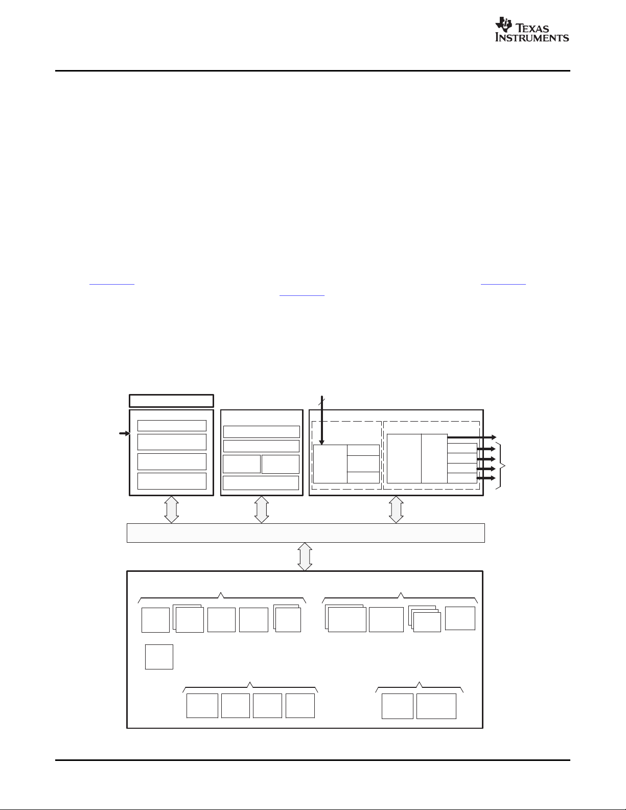
Introduction
1.1 Introduction
1.2 Block Diagram
The TMS320DM643x Digital Media Processor (DMP) contains a powerful DSP to efficiently handle image,
video, and audio processing tasks. The DM643x DMP consists of the following primary components and
sub-systems:
• DSP Subsystem (DSPSS), including the C64x+ Megamodule and associated memory.
• Video Processing Subsystem (VPSS), including the Video Processing Front End (VPFE) Subsystem,
Image Input and Image Processing Subsystem, and the Video Processing Back End (VPBE) Display
Subsystem
• A set of I/O peripherals
• A powerful DMA subsystem and DDR2 memory controller interface
The DSP subsystem includes TI’s standard TMS320C64x+ Megamodule and several blocks of internal
memory (L1P, L1D, and L2).
For more information, see the TMS320C64x+ DSP Megamodule Peripherals Reference Guide
(SPRU871 ), the TMS320C64x/C64x+ DSP CPU and Instruction Set Reference Guide (SPRU732 ), and the
TMS320C64x+ DSP Cache User’s Guide (SPRU862 ).
An example block diagram for the TMS320DM643x DMP is shown in Figure 1-1 .
Figure 1-1. TMS320DM643x DMP Block Diagram
Introduction 12 SPRU978E – March 2008
Submit Documentation Feedback
Page 13

www.ti.com
1.3 DSP Subsystem in TMS320DM643x DMP
In the DM643x DMP, the DSP subsystem is responsible for performing digital signal processing for digital
media applications. In addition, the DSP subsystem acts as the overall system controller, responsible for
handling many system functions such as system-level initialization, configuration, user interface, user
command execution, connectivity functions, and overall system control.
1.3.1 Components of the DSP Subsystem
The DSP subsystem in the DM643x DMP consists of the following components:
• C64x+ Megamodule
• DSP Internal Memories
– Level-1 program memory (L1P)
– Level-1 data memory (L1D)
– Level-2 unified memory (L2)
The DSP also manages/controls all peripherals on the device. Refer to device-specific data manual for the
full list of peripherals.
Figure 1-1 shows the functional block diagram of the DM643x DMP and how the DSP subsystem is
connected to the rest of the device. The DM643x DMP architecture uses the System Infrastructure
(Switched Central Resource) to transfer data within the system.
Chapter 2 discusses the C64x+ Megamodule in more details, including its detailed block diagram.
DSP Subsystem in TMS320DM643x DMP
SPRU978E – March 2008 Introduction 13
Submit Documentation Feedback
Page 14

Introduction 14 SPRU978E – March 2008
Submit Documentation Feedback
Page 15

SPRU978E – March 2008
TMS320C64x+ Megamodule
Topic .................................................................................................. Page
2.1 Introduction .............................................................................. 16
2.2 TMS320C64x+ CPU .................................................................... 16
2.3 Memory Controllers ................................................................... 18
2.4 Internal Peripherals ................................................................... 22
Chapter 2
SPRU978E – March 2008 TMS320C64x+ Megamodule 15
Submit Documentation Feedback
Page 16

www.ti.com
Introduction
2.1 Introduction
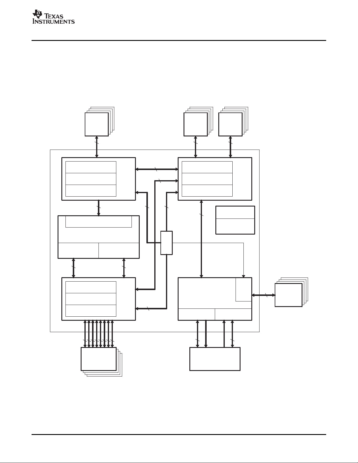
The C64x+ Megamodule (Figure 2-1 ) consists of the following components:
• TMS320C64x+ CPU
• Internal memory controllers:
– Level-1 program memory controller (L1P controller)
– Level-1 data memory controller (L1D controller)
– Level-2 unified memory controller (L2 controller)
– External memory controller (EMC)
– Internal direct memory access (IDMA) controller
• Internal peripherals
– Interrupt controller (INTC)
– Power-down controller (PDC)
2.2 TMS320C64x+ CPU
The C64x+ Megamodule includes the C64x+ CPU. The C64x+ CPU is a member of the TMS320C6000™
generation of devices. The C6000™ devices execute up to eight 32-bit instructions per cycle. The CPU
consists of 64 general-purpose 32-bit registers and eight functional units. The eight functional units contain
two multipliers and six ALUs. For more information on the CPU, see the TMS320C64x/C64x+ DSP CPU
and Instruction Set Reference Guide (SPRU732 ).
Features of the C6000 devices include:
• Advanced VLIW CPU with eight functional units, including two multipliers and six arithmetic units
– Executes up to eight instructions per cycle for up to ten times the performance of typical DSPs
– Allows designers to develop highly effective RISC-like code for rapid development time
• Instruction packing
– Gives code-size equivalence for eight instructions that execute serially or in parallel
– Reduces code size, program fetches, and power consumption
• Conditional execution of most instructions
– Reduces costly branching
– Increases parallelism for higher sustained performance
• Efficient code execution on independent functional units
– Industry's most efficient C compiler on DSP benchmark suite
– Industry's first assembly optimizer for rapid development and improved parallelization
• 8/16/32-bit data support, providing efficient memory support for a variety of applications
• 40-bit arithmetic options add extra precision for vocoders and other computationally intensive
applications
• Saturation and normalization provide support for key arithmetic operations
• Field manipulation and instruction extract, set, clear, and bit counting support a common operation
found in control and data manipulation applications
The C64x+ devices include the following additional features:
• Each multiplier can perform two 16 × 16-bit or four 8 × 8-bit multiplies every clock cycle
• Quad 8-bit and dual 16-bit instruction set extensions with data flow support
• Support for nonaligned 32-bit (word) and 64-bit (double word) memory accesses
• Special communication-specific instructions to address common operations in error-correcting codes
• Bit count and rotate hardware extends support for bit-level algorithms
• Compact instructions: common instructions (AND, ADD, LD, MPY) have 16-bit versions to reduce code
size
16 TMS320C64x+ Megamodule SPRU978E – March 2008
Submit Documentation Feedback
Page 17
www.ti.com
Cache control
Memory protect
Bandwidth mgmt
L1P
RAM/
cache
256
Bandwidth mgmt
Memory protect
Cache control
256
L2
256
RAM/
Cache
ROM
256
Instruction fetch
file A file B
C64x+ CPU
256
Cache control
Memory protect
Bandwidth mgmt
L1D
128 128
8 x 32
IDMA
256
256
128
256
Power down
Interrupt
controller
CFG
MDMA SDMA
EMC
256
32
Chip
registers
64 64
RAM/
cache
Register Register
System
infrastructure
• Protected mode operation: a two-level system of privileged program execution to support higher
capability operating systems and system features, such as memory protection
• Exceptions support for error detection and program redirection to provide robust code execution
• Hardware support for modulo loop operation to reduce code size
• Industry's first assembly optimizer for rapid development and improved parallelization
Figure 2-1. TMS320C64x+ Megamodule Block Diagram
TMS320C64x+ CPU
SPRU978E – March 2008 TMS320C64x+ Megamodule 17
Submit Documentation Feedback
Page 18

www.ti.com
Memory Controllers
2.3 Memory Controllers
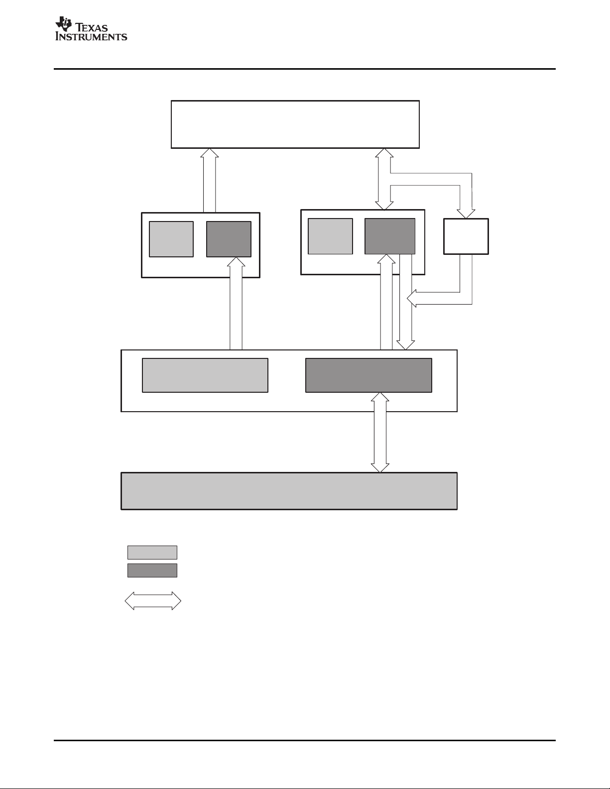
The C64x+ Megamodule implements a two-level internal cache-based memory architecture with external
memory support. Level 1 memory is split into separate program memory (L1P memory) and data memory
(L1D memory). Figure 2-2 shows a diagram of the memory architecture. L1P and L1D are configurable as
part L1 RAM (normal addressable on-chip memory) and part L1 cache. L1 memory is accessible to the
CPU without stalls. Level 2 memory (L2) can also be split into L2 RAM (normal addressable on-chip
memory) and L2 cache for caching external memory locations.
The following controllers manage RAM/cache configuration and cache data paths:
• L1P controller
• L1D controller
• L2 controller
• External memory controller (EMC)
The internal direct memory access (IDMA) controller manages DMA among the L1P, L1D, and L2
memories.
This section briefly describes the cache and DMA controllers. For detailed information about each of these
controllers, see the TMS320C64x+ DSP Cache User’s Guide (SPRU862 ) and the TMS320C64x+ DSP
Megamodule Reference Guide (SPRU871 ).
Note: The C64x+ Megamodule includes the memory controllers; however, the physical L1P, L1D,
and L2 memories are not part of the megamodule, even though they reside in the DSP
subsystem. Thus, the physical memories are described separately because the C64x+
Megamodule supports a variety of memory configurations. Refer to Section 3.1 for more
information on the L1P, L1D, and L2 memory configuration specific to the DM643x DMP.
2.3.1 L1P Controller
The L1P controller is the hardware interface between level 1 program memory (L1P memory) and the
other components in the C64x+ Megamodule (for example, C64x+ CPU, L2 controller, and EMC). The
L1P controller responds to instruction fetch requests from the C64x+ CPU and manages transfer
operations between L1P memory and the L2 controller and between L1P memory and the EMC.
Refer to the device-specific data manual for the amount of L1P memory on the device. The L1P controller
has a register interface that allows you to configure part or all of the L1P RAM as normal RAM or as
cache. You can configure cache sizes of 0 KB, 4 KB, 8 KB, 16 KB, or 32 KB of the RAM.
The L1P is divided into two regions—denoted L1P region 0 and L1P region 1. This is the L1P architecture
on the DM643x DMP:
• L1P region 0: Not populated with memory.
• L1P region 1: Populated with memory that can be configured as mapped memory or cache. The L1P
region 1 memory has 0 wait state. This region is shown as “L1P RAM/Cache” in the device-specific
data manual.
The DM643x DMP does not support the L1P memory protection feature of the standard
C64x+ Megamodule.
Refer to the TMS320C64x+ DSP Cache User’s Guide (SPRU862 ) and to the L1P controller section of the
TMS320C64x+ DSP Megamodule Reference Guide (SPRU871 ) for more information on the L1P controller
and for a description of its control registers.
18 TMS320C64x+ Megamodule SPRU978E – March 2008
Submit Documentation Feedback
Page 19
www.ti.com
C64x+ CPU
Fetch Path Data Path
Write
Buffer
L1D
Cache
L1D
SRAM
L1 Data
L1P
Cache
L1P
SRAM
L1 Program
L2 Cache
L2 SRAM
L2 Unified Data/Program Memory
External Memory
64 bit
256 bit
128 bit
256 bit
256 bit
2 x 64 bit
Legend:
addressable memory
cache memory
data paths managed by
cache controller
256 bit
Figure 2-2. C64x+ Cache Memory Architecture
Memory Controllers
SPRU978E – March 2008 TMS320C64x+ Megamodule 19
Submit Documentation Feedback
Page 20

www.ti.com
Memory Controllers
2.3.2 L1D Controller
The L1D controller is the hardware interface between level 1 data memory (L1D memory) and the other
components in the C64x+ Megamodule (for example, C64x+ CPU, L2 controller, and EMC). The L1D
controller responds to data requests from the C64x+ CPU and manages transfer operations between L1D
memory and the L2 controller and between L1D memory and the EMC.
Refer to the device-specific data manual for the amount of L1D memory on the device. The L1D controller
has a register interface that allows you to configure part of the L1D RAM as normal data RAM or as
cache. You can configure cache sizes of 0 KB, 4 KB, 8 KB, 16 KB, or 32 KB of the RAM.
The L1D is divided into two regions—denoted L1D region 0 and L1D region 1. This is the L1D architecture
on the DM643x DMP:
• L1D region 0: On some DM643x devices, this region is populated with mapped memory. If it is
populated with memory, this region is shown as “L1D RAM” in the device-specific data manual.
• L1D region 1: Populated with memory that can be configured as mapped memory or cache. This
region is shown as “L1D RAM/Cache” in the device-specific data manual.
The DM643x DMP does not support the L1D memory protection features of the standard
C64x+ Megamodule.
Refer to the TMS320C64x+ DSP Cache User’s Guide (SPRU862 ) and to the L1D controller section of the
TMS320C64x+ DSP Megamodule Reference Guide (SPRU871 ) for more information on the L1D controller
and for a description of its control registers.
2.3.3 L2 Controller
The L2 controller is the hardware interface between level 2 memory (L2 memory) and the other
components in the C64x+ Megamodule (for example, L1P controller, L1D controller, and EMC). The L2
controller manages transfer operations between L2 memory and the other memory controllers (L1P
controller, L1D controller, and EMC).
Refer to device-specific data manual for the amount of L2 memory on the device. The L2 controller has a
register interface that allows you to configure part or all of the L2 RAM as normal RAM or as cache. You
can configure cache sizes of 0 KB, 32 KB, 64 KB, or 128 KB of the RAM.
The L2 memory implements two separate memory ports. This is the L2 architecture on the DM643x DMP:
• Port 0
– Shown as “L2 RAM/Cache” in the device-specific data manual.
– Banking scheme: 2 × 128-bit banks
– Latency: 1 cycle (0 wait state)
• Port 1
– Shown as “Boot ROM” in the device-specific data manual.
– Banking scheme: 1 × 256-bit bank
– Latency: 1 cycle (0 wait state)
The DM643x DMP does not support the L2 memory protection feature of the standard
C64x+ Megamodule.
Refer to the TMS320C64x+ DSP Cache User’s Guide (SPRU862 ) and to the L2 controller section of the
TMS320C64x+ DSP Megamodule Reference Guide (SPRU871 ) for more information on the L2 controller
and for a description of its control registers.
TMS320C64x+ Megamodule20 SPRU978E – March 2008
Submit Documentation Feedback
Page 21

www.ti.com
2.3.4 External Memory Controller (EMC)
The external memory controller (EMC) is the hardware interface between the external memory map
(external memory and external registers) and the other controllers in the C64x+ Megamodule (for
example, L1P controller, L1D controller, and L2 controller). The EMC manages transfer operations
between external memory and registers and the other memory controllers (L1P controller, L1D controller,
and EMC).
EMC does not support the memory protection feature of the standard C64x+ Megamodule.
Refer to the TMS320C64x+ DSP Cache User’s Guide (SPRU862 ) and to the TMS320C64x+ DSP
Megamodule Reference Guide (SPRU871 ) for more information on the EMC and for a description of its
control registers.
2.3.5 Internal DMA (IDMA)
The internal DMA (IDMA) controller facilitates DMA transfers between any two internal memory-mapped
locations. Internal memory-mapped locations include L1P, L1D, L2, and internal peripheral configuration
registers.
Note: The IDMA cannot facilitate DMA to or from external memory-mapped locations. The EDMA
facilitates external DMA transfers. Refer to Section 3.1 and to the TMS320DM643x DMP
Enhanced Direct Memory Access (EDMA) Controller User's Guide (SPRU987 ) for
information on EDMA.
The IDMA controller enables the rapid paging of data sections to any local memory-mapped RAM. A key
advantage of the IDMA is that it allows paging between slower L2 and faster L1D data memory. These
transfers take place without CPU intervention and without cache stalls.
Another key advantage is that you can use the IDMA controller to program internal peripheral
configuration registers without CPU intervention.
Refer to the internal DMA (IDMA) controller section in the TMS320C64x+ DSP Megamodule Reference
Guide (SPRU871 ) for more information on the IDMA controller and for a description of its control registers.
Memory Controllers
SPRU978E – March 2008 TMS320C64x+ Megamodule 21
Submit Documentation Feedback
Page 22

www.ti.com
Internal Peripherals
2.4 Internal Peripherals
This C64x+ Megamodule includes the following internal peripherals:
• Interrupt controller (INTC)
• Power-down controller (PDC)
This section briefly describes the INTC and PDC. For more information on these peripherals, see the
TMS320C64x+ DSP Megamodule Reference Guide (SPRU871 ).
2.4.1 Interrupt Controller (INTC)
The C64x+ Megamodule includes an interrupt controller (INTC) to manage CPU interrupts. The INTC
maps the 0 to 127 DSP device events to 12 CPU interrupts. Refer to device-specific data manual for a list
of all the DSP device events. The interrupt controller section of the TMS320C64x+ DSP Megamodule
Reference Guide (SPRU871 ) fully describes the INTC and how it maps the DSP device events to the
12 CPU interrupts.
2.4.2 Power-Down Controller (PDC)
The C64x+ Megamodule includes a power-down controller (PDC). The PDC can power-down all of the
following components of the C64x+ Megamodule:
• C64x+ CPU
• L1P controller
• L1D controller
• L2 controller
• Extended memory controller (EMC)
• Internal direct memory access (IDMA) controller
The DM643x DMP does not support power-down of the internal memories of the DSP subsystem.
The C64x+ Megamodule is capable of providing both dynamic and static power-down; however, only static
power-down is supported on the DM643x DMP. The TMS320C64x+ DSP Megamodule Reference Guide
(SPRU871 ) describes the power-down control in more detail.
• Static power-down: The PDC initiates power down of the entire C64x+ Megamodule and all internal
memories immediately upon command from software.
On the DM643x DMP, static power-down affects all components of the C64x+ Megamodule. The DM643x
DMP does not support power-down of the internal memories. Software can initiate static power-down via a
register bit in the PDC register. For more information on the PDC, see the TMS320C64x+ DSP
Megamodule Reference Guide (SPRU871 ).
Note: The DM643x DMP does not support dynamic power-down.
TMS320C64x+ Megamodule22 SPRU978E – March 2008
Submit Documentation Feedback
Page 23

www.ti.com
2.4.3 Bandwidth Manager
The bandwidth manager provides a programmable interface for optimizing bandwidth among the
requesters for resources, which include the following:
• EDMA-initiated DMA transfers (and resulting coherency operations)
• IDMA-initiated transfers (and resulting coherency operations)
• Programmable cache coherency operations
• CPU direct-initiated transfers
The resources include the following:
• L1P memory
• L1D memory
• L2 memory
• Resources outside of C64x+ Megamodule: external memory, on-chip peripherals, registers
Since any given requestor could potentially block a resource for extended periods of time, the bandwidth
manager is implemented to assure fairness for all requesters.
The bandwidth manager implements a weighted-priority-driven bandwidth allocation. Each requestor
(EDMA, IDMA, CPU, etc.) is assigned a priority level on a per-transfer basis. The programmable priority
level has a single meaning throughout the system. There are a total of nine priority levels, where priority
zero is the highest priority and priority eight is the lowest priority. When requests for a single resource
contend, access is granted to the highest-priority requestor. When the contention occurs for multiple
successive cycles, a contention counter assures that the lower-priority requestor gets access to the
resource every 1 out of n arbitration cycles, where n is programmable. A priority level of -1 represents a
transfer whose priority has been increased due to expiration of the contention counter or a transfer that is
fixed as the highest-priority transfer to a given resource.
Internal Peripherals
– Block based coherency operations
– Global coherency operations
– Data access (load/store)
– Program access
SPRU978E – March 2008 TMS320C64x+ Megamodule 23
Submit Documentation Feedback
Page 24

TMS320C64x+ Megamodule24 SPRU978E – March 2008
Submit Documentation Feedback
Page 25

SPRU978E – March 2008
System Memory
Topic .................................................................................................. Page
3.1 Memory Map ............................................................................. 26
3.2 Memory Interfaces Overview ...................................................... 27
Chapter 3
SPRU978E – March 2008 System Memory 25
Submit Documentation Feedback
Page 26

www.ti.com
Memory Map
3.1 Memory Map
Refer to your device-specific data manual for memory-map information.
3.1.1 DSP Internal Memory (L1P, L1D, L2)
This section describes the configuration of the DSP internal memory in the DM643x DMP that consists of
L1P, L1D, and L2. In the DM643x DMP:
• L1P memory: The L1P controller allows you to configure part or all of the L1P RAM as normal program
RAM or as direct mapped cache. You can configure cache sizes of 0 KB, 4 KB, 8 KB, 16 KB, or 32 KB
of the RAM.
• L1D memory: The L1D controller allows you to configure part of the L1D RAM as normal data RAM or
as cache. You can configure cache sizes of 0 KB, 4 KB, 8 KB, 16 KB, or 32 KB of the RAM.
• L2 memory: The L2 controller allows you to configure part or all of the L2 RAM as normal RAM or as
cache. You can configure cache sizes of 0 KB, 32 KB, 64 KB, or 128 KB of the RAM.
Refer to device-specific data manual for the exact amount of RAM/cache. Refer to TMS320C64x+ DSP
Megamodule Reference Guide (SPRU871 ) for information on how to configure the cache.
3.1.2 External Memory
The DSP has access to the following external memories:
• DDR2 synchronous DRAM
• Asynchronous EMIF/NOR/NAND Flash
The external memory controller (EMC) facilitates DSP access to these memories in the C64x+
Megamodule. The following external memories are accessible to the DSP:
• DDR2 port
• Asynchronous EMIF (for example, NOR and NAND Flash in 4 EM_CS regions)
For the memory-map locations of these external memories, refer to the memory-map section of the
device-specific data manual.
3.1.3 Internal Peripherals
3.1.4 Device Peripherals
The following internal peripherals are accessible to the DSP:
• Power-down controller (PDC)
• Interrupt controller (INTC)
For more information on the internal peripherals, see the TMS320C64x+ DSP Megamodule Reference
Guide (SPRU871 ).
The DSP has access to all peripherals on the device. Refer to device-specific data manual for the full list
of peripherals.
System Memory26 SPRU978E – March 2008
Submit Documentation Feedback
Page 27

www.ti.com
3.2 Memory Interfaces Overview
This section describes the different memory interfaces of DM643x DMP. The DM643x DMP supports
several memory and external device interfaces, including the following:
• DDR2 synchronous DRAM
• Asynchronous EMIF/NOR/NAND Flash
3.2.1 DDR2 External Memory Interface
The DDR2 external memory interface (EMIF) port is a dedicated interface to DDR2 SDRAM. It supports
JESD79D-2A standard compliant DDR2 SDRAM devices and can support either 16-bit or 32-bit interfaces.
DDR2 SDRAM plays a key role in a DM643x DMP-based system. Such a system is expected to require a
significant amount of high-speed external memory for the following:
• Buffering input image data from sensors or video sources
• Intermediate buffering for processing/resizing of image data in the video processing front end (VPFE)
• Video processing back end (VPBE) display buffers
• Intermediate buffering for large raw Bayer data image files while performing still camera processing
functions
• Buffering for intermediate data while performing video encode and decode functions
• Storage of executable firmware for DSP
3.2.2 External Memory Interface
The DM643x DMP external memory interface (EMIF) provides an 8-bit data bus, an address bus width of
up to 24-bits, and 4 dedicated chip selects, along with memory control signals. These signals are statically
multiplexed between the asynchronous EMIF (EMIFA) module that provides asynchronous EMIF and
NAND interfaces.
The EMIFA signals are multiplexed with other peripheral signals on the device. Refer to device-specific
data manual for details on pin multiplexing.
Memory Interfaces Overview
3.2.2.1 Asynchronous EMIF Interface
The asynchronous EMIF (EMIFA) interface provides both the asynchronous EMIF and NAND interfaces.
Four chip selects are provided. Each is individually configurable to provide either asynchronous EMIF or
NAND support.
• The asynchronous EMIF mode supports asynchronous devices (RAM, ROM, and NOR Flash)
• 64MB asynchronous address range over 4 chip selects (16MB each)
• Supports 8-bit data bus width
• Programmable asynchronous cycle timings
• Supports extended waits
• Supports Select Strobe mode
• Supports TI DSP HPI interface
• Supports booting DM643x DMP from CS2 (SRAM/NOR Flash)
3.2.2.2 NAND Interface
The asynchronous EMIF (EMIFA) interface provides both the asynchronous EMIF and NAND interfaces.
Four chip selects are provided and each is individually configurable to provide either EMIFA or NAND
support.
• The NAND mode supports NAND Flash on up to 4 asynchronous chip selects
• Supports 8-bit data bus width
• Programmable cycle timings
• Performs ECC calculation
• Bootloader code in Boot ROM supports booting of the DM643x DMP from NAND-Flash located at CS2
SPRU978E – March 2008 System Memory 27
Submit Documentation Feedback
Page 28

System Memory28 SPRU978E – March 2008
Submit Documentation Feedback
Page 29

SPRU978E – March 2008
Device Clocking
Topic .................................................................................................. Page
4.1 Overview .................................................................................. 30
4.2 Clock Domains ......................................................................... 30
Chapter 4
SPRU978E – March 2008 Device Clocking 29
Submit Documentation Feedback
Page 30

www.ti.com
Overview
4.1 Overview
The DM643x DMP requires one primary reference clock. The primary reference clock can be either crystal
input or driven by external oscillators. A 27 MHZ crystal at the MXI/CLKIN pin is recommended for the
system PLLs, which generate the clocks for the DSP, peripherals, DMA, and imaging peripherals. The
recommended 27 MHZ input enables you to use the video DACs to drive NTSC/PAL television signals at
the proper frequencies.
For detailed specifications on clock frequency and voltage requirements, see the device-specific data
manual.
There are two clocking modes:
• PLL Bypass Mode - power saving (device defaults to this mode)
• PLL Mode - PLL multiplies input clock up to the desired operating frequency
The clock of the major chip subsystems must be programmed to operate at fixed ratios of the primary
system/DSP clock frequency within each mode, as shown in Table 4-1 . The DM643x DMP clocking
architecture is shown in Figure 4-1 .
Table 4-1. System Clock Modes and Fixed Ratios for Core Clock Domains
Subsystem Core Clock Domain Fixed Ratio vs. DSP frequency
DSP CLKDIV1 1:1
EDMA CLKDIV3 1:3
VPSS
Peripherals (CLKDIV3 domain) CLKDIV3 1:3
Peripherals (CLKDIV6 domain) CLKDIV6 1:6
4.2 Clock Domains
4.2.1 Core Domains
The core domains refer to the clock domains for all of the internal processing elements of the DM643x
DMP, such as the DSP/EDMA/peripherals, etc. All internal communications between DSP and modules
operate at core domain clock frequencies. All of the core clock domains are synchronous to each other,
come from a single PLL (PLL1), have aligned clock edges, and have fixed divide by ratio requirements, as
shown in Table 4-1 and Figure 4-1 . It is user's responsibility to ensure the fixed divide ratios between
these core clock domains are achieved.
The DSP is in the CLKDIV1 domain and receives the PLL1 frequency directly (PLLDIV1 of PLL controller
1 (PLLC1) set to divide by 1), or receives the divided-down PLL1 frequency (PLLDIV1 of PLLC1 set to
divide by 2, 3, etc.). The DSP has internal clock dividers that it uses to create the DSP ÷ 3 clock frequency
to communicate with other components on-chip.
Modules in the CLKDIV3 domain (for example, EDMA, VPSS, CLKDIV3 domain peripherals) must run at
1/3 the DSP frequency.
Modules in the CLKDIV6 domain (for example, CLKDIV6 domain peripherals) must run at 1/6 the DSP
frequency.
Modules in the CLKIN domain (for example, UART, Timer, I2C, PWM, HECC) run at the MXI/CLKIN
frequency, asynchronous to the DSP. There is no fixed ratio requirement between these peripherals
frequencies and the DSP frequency.
Refer to device-specific data manual for the core clock domain for each peripheral.
30 Device Clocking SPRU978E – March 2008
Submit Documentation Feedback
Page 31

www.ti.com
DSP Subsystem
SYSCLK1
SYSCLK3
SCR
EDMA
VPFE
VPBE
DACs
DDR2 PHY
DDR2 VTP
DDR2 Memory
controller
PLLDIV2 (/10)
PLLDIV1 (/2)
BPDIV
PLL Controller 2
PLL Controller 1
PLLDIV2 (/3)
PLLDIV3 (/6)
PLLDIV1 (/1)
SYSCLK2
UARTs (x2)
I2C
Timers (x3)
PWMs (x3)
EMAC
EMIFA
VLYNQ
HPI
McASP0
McBSP0
GPIO
McBSP1
PCI
MXI/CLKIN
(27 MHz)
PCLK
VPBECLK
OSCDIV1 (/1)
HECC
OBSCLK
(CLKOUT0 Pin)
BPDIV (/1)
SYSCLKBP
AUXCLK
Figure 4-1. Overall Clocking Diagram
Clock Domains
SPRU978E – March 2008 Device Clocking 31
Submit Documentation Feedback
Page 32

www.ti.com
Clock Domains
4.2.2 Core Frequency Flexibility
The core frequency domain clocks are supplied by the PLL controller 1 (PLLC1). These domain clocks are
flexible, to a degree, within the limitations specified in the device-specific data manual. All of the following
frequency ranges and multiplier/divider ratios in the data manual must be adhered to:
• Input clock frequency range (MXI/CLKIN)
• PLL1 multiplier (PLLM) range
• PLL1 output (PLLOUT) frequency range based on the core voltage (1.05V or 1.2V) of the device
• Maximum device speed
• PLLC1's SYSCLK3:SYSCLK2:SYSCLK1 frequency ratio must be fixed to 1:3:6. For example, if
SYSCLK1 is at 600 MHZ, SYSCLK2 must be at 200 MHZ, and SYSCLK3 must be at 100 MHZ.
As specified in the data manual, the PLLs can be driven by any input ranging from 20 to 30 MHZ.
However, a 27 MHZ input is required if the video processing back end (VPBE) subsystem is needed to
drive television displays with the integrated video DACs.
Table 4-2 shows some example PLL1 multiplier and divider settings assuming MXI/CLKIN frequency of 27
MHZ. The Applicable to Device Core Voltage column indicates whether the setting is allowed for a given
device core voltage. For example, the last row in Table 4-2 (PLL1 multiplier 22 for a 27 MHZ clock input)
only applies to devices with a core voltage 1.2V to meet the PLL1 output (PLLOUT) frequency range
required in the data manual. In addition, you must ensure the SYSCLK1 frequency does not exceed the
speed grade of the device. For example, for a device rated at 400 MHZ speed grade, SYSCLK1 must not
exceed 400 MHZ.
PLL1 PLLOUT Freq Freq Freq
Multiplier Freq (MHZ) Divider
15 405.0 1 405.0 3 135.0 6 67.5 Y Y
16 432.0 1 432.0 3 144.0 6 72.0 Y Y
17 459.0 1 459.0 3 153.0 6 76.5 Y Y
18 486.0 1 486.0 3 162.0 6 81.0 Y Y
19 513.0 1 513.0 3 171.0 6 85.5 Y Y
20 540.0 1 540.0 3 180.0 6 90.0 Y 21 567.0 1 567.0 3 189.0 6 94.5 Y 22 594.0 1 594.0 3 198.0 6 99.0 Y 22 594.0 2 297.0 6 99.0 12 49.5 Y -
Table 4-2. Example PLL1 Frequencies and Dividers (27 MHZ Clock Input)
CLKDIV1 Domain CLKDIV3 Domain CLKDIV6 Domain Applicable to Device
(SYSCLK1) (SYSCLK2) (SYSCLK3) Core Voltage
PLL1
(1)
(MHZ) Divider
(1)
(MHZ) Divider
(1)
(MHZ) 1.2V 1.05V
(1)
The RATIO bit in PLLDIV n is programmed as Divider - 1. For example, for a SYSCLK1 divider of 1, you should program
PLLDIV1.RATIO = 0, PLLDIV2.RATIO = 2, PLLDIV3.RATIO = 5.
32 Device Clocking SPRU978E – March 2008
Submit Documentation Feedback
Page 33

www.ti.com
4.2.3 DDR2/EMIF Clock
The DDR2 interface has a dedicated clock driven from PLL2. This is a separate clock system from the
PLL1 clocks provided to other components of the system. This dedicated clock allows the reduction of the
core clock rates to save power while maintaining the required minimum clock rate (125 MHZ) for DDR2.
PLL2 must be configured to output a 2 × clock to the DDR2 PHY interface.
The DM643x DMP video DACs are capable of driving high quality progressive television displays, if driven
by a 54 MHZ input clock sourced by PLL2 (see the TMS320DM643x DMP Video Processing Back End
(VPBE) User's Guide (SPRU952 ) for more detailed information). This will limit the possible PLL2 settings
to a multiple of 54 MHZ so that the VPBE clock can be derived with a simple integer clock divider.
All of the following frequency ranges and multiplier/divider ratios in the device-specific data manual must
be adhered to when configuring PLL2:
• Input clock frequency range (MXI/CLKIN)
• PLL2 multiplier (PLLM) range
• PLL2 output (PLLOUT) frequency range based on core voltage (1.05V or 1.2V) of the device
Table 4-3 and Table 4-4 show some PLL2/DDR2 clock rates assuming a MXI/CLKIN frequency of 27
MHZ. These tables also indicate settings that are multiples of 54 MHZ.
PLL2 Multiplier (MHZ) Divider
Table 4-3. Example PLL2 Frequencies (Core Voltage = 1.2V)
PLL2 PLLOUT Freq SYSCLK1 PHY [2 × clock]
28 756.0 3 252.0 126.0 Yes
19 513.0 2 256.5 128.3 No
29 783.0 3 261.0 130.5 No
20 540.0 2 270.0 135.0 Yes
31 837.0 3 279.0 139.5 No
21 567.0 2 283.5 141.8 No
32 864.0 3 288.0 144.0 Yes
22 594.0 2 297.0 148.5 Yes
23 621.0 2 310.5 155.3 No
24 648.0 2 324.0 162.0 Yes
25 675.0 2 337.5 168.8 No
(1)
(MHZ) DDR2 Clock (MHZ) 54 MHZ Multiple
Clock Domains
(1)
The RATIO bit in PLLDIV n is programmed as Divider - 1. For example, for SYSCLK1 divider of 3, you should program
PLLDIV1.RATIO = 2.
Table 4-4. Example PLL2 Frequencies (Core Voltage = 1.05V)
PLL2 Multiplier (MHZ) Divider
19 513.0 2 256.5 128.3 No
20 540.0 2 270.0 135.0 Yes
21 567.0 2 283.5 141.8 No
22 594.0 2 297.0 148.5 Yes
23 621.0 2 310.5 155.3 No
24 648.0 2 324.0 162.0 Yes
(1)
The RATIO bit in PLLDIV n is programmed as Divider - 1. For example, for SYSCLK1 divider of 3, you should program
PLLDIV1.RATIO = 2.
SPRU978E – March 2008 Device Clocking 33
Submit Documentation Feedback
PLL2 PLLOUT Freq SYSCLK1 PHY [2 × clock]
(1)
(MHZ) DDR2 Clock (MHZ) 54 MHZ Multiple
Page 34

www.ti.com
Clock Domains
4.2.4 I/O Domains
The I/O domains refer to the frequencies of the peripherals that communicate through device pins. In
many cases, there are frequency requirements for a peripheral pin interface that are set by an outside
standard and must be met. It is not necessarily possible to obtain these frequencies from the on-chip clock
generation circuitry, so the frequencies must be obtained from external sources and are asynchronous to
the core frequency domain by definition.
Table 4-5 lists peripherals with external I/O interface, and their I/O domain clock/frequency. It also shows
the core clock domain as a reference to show the core clock used for internal communications. See
section Section 4.2.1 for more details on core clock domains. See device-specific data manual for the
exact I/O clock frequency supported on the device.
Table 4-5. Peripheral I/O Domain Clock
Peripheral Frequency Internal Clock Source External Clock Source Core Clock Domain
I/O Domain Clock
DDR2 125-166 MHZ PLLC2 SYSCLK1 — CLKDIV3
VPFE 10-98 MHZ — PCLK CLKDIV3
VPBE 6.25-75 MHZ PLLC1 SYSCLKBP VPBECLK CLKDIV3
PCI 33 MHZ — PCICLK CLKDIV3
EMAC 25 MHZ — MTXCLK, MRXCLK CLKDIV6
VLYNQ up to 80 MHZ PLLC1 SYSCLK3 VLYNQ_CLOCK CLKDIV6
McBSP up to 40 MHZ PLLC1 SYSCLK3 CLKS, CLKX, CLKR CLKDIV6
McASP up to 40 MHZ PLLC1 SYSCLK3 AHCLKX, AHCLKR, CLKDIV6
GPIO NA (asynchronous — — CLKDIV6
interface)
EMIFA NA (asynchronous — — CLKDIV6
interface)
HPI NA (asynchronous — — CLKDIV6
interface)
I2C up to 400 kHz MXI/CLKIN SCL CLKIN
Timer output up to 1/2 CLKIN MXI/CLKIN TINP0L (Timer 0), CLKIN
frequency (typically 27 MHZ) TINP1L (Timer 1)
input up to 1/4 CLKIN
frequency
Watchdog Timer NA MXI/CLKIN — CLKIN
PWM NA — — CLKIN
UART NA — — CLKIN
HECC NA — — CLKIN
I/O (External) Domain Clock Source Options
(typically 27 MHZ)
PLLC2 SYSCLK2 PCLK
(typically 54 MHZ)
ACLKX, ACLKR
(typically 27 MHZ)
(typically 27 MHZ)
34 Device Clocking SPRU978E – March 2008
Submit Documentation Feedback
Page 35

www.ti.com
4.2.5 Video Processing Back End
3
2
0
1
0
1
2
PLLDIV2
CLK54
PLL2
DDR_CLKx2
PCLK
VPBECLK
MXI
CLK_VENC
CLK_DAC
1
0
venc_sclk_enc
CG OSD
VENC
DACs
venc_div2
venc_sclk_osd
VPSS
VPSS_CLKCTL.MUXSEL
CLK54 CLK_VENC CLK_DAC
0 27 MHzOff 27 MHz
1h 54 54 MHz 54 MHz
2h Off VPBECLK VPBECLK
3h Off PCLK Off
PLLDIV1
PLLC1
SYSCLKBP
VPSS_CLKCTL.MUXSEL
The video processing back end (VPBE) is a submodule of the video processing subsystem (VPSS). The
VPBE must interface with a variety of LCDs, as well as the 4-channel DAC module. There are many
different types of LCDs, which require many different specific frequencies. The range of frequencies that
the pin interface needs to run is 6.25 MHZ to 75 MHZ.
There are two asynchronous clock domains in the VPBE: the external clock domain (6.25 MHZ to 75
MHZ) and the internal (system) clock domain, which is at the DSP ÷ 3 clock rate.
The external clock domain can get its clock from 4 sources:
• PLLC1 SYSCLKBP (typically 27 MHZ, MXI/CLKIN divide by 1)
• The VPBECLK input pin
• The VPFE pixel clock input (PCLK)
• PLLC2 SYSCLK2 (a divide down from PLL2)
The 4 DACs are hooked up to the VENC module that is in the VPBE. The data flow between the VPBE
and DACs is synchronous. The various possible clocking modes are shown in Figure 4-2 and described in
Table 4-6 .
The DACs can have their clocks independently gated off when the DACs are not being used. This is
described in Chapter 7 .
Clock Domains
Figure 4-2. VPBE/DAC Clocking
SPRU978E – March 2008 Device Clocking 35
Submit Documentation Feedback
Page 36

www.ti.com
Clock Domains
Table 4-6. Possible Clocking Modes
VPSS_CLKCTL.MUXSEL Bit Clocking Mode Description
0 MXI mode Both the VENC and the DAC get their clock from PLLC1 SYSCLKBP, which
1h PLL2 mode The PLL2 (divided-down) generates a 54 MHZ clock. Both the DAC and the
2h VPBECLK mode Both the DAC and the VENC receive the VPBECLK. The VENC has the
3h PCLK mode The VENC receives the PCLK. The DAC receives no clock, and should be
defaults to the MXI 27 MHZ crystal input divide by 1.
VENC receive the 54 MHZ. The VENC can optionally divide it by 2 to create a
27 MHZ clock. Note this mode requires the DDR2 clock setting (from PLL2) to
be an even multiple of 27 MHZ so that an integer divisor can be used to
create the 54 MHZ DAC clock. Thus, this mode limits the available DDR2
clock frequencies.
option of dividing it by 2 for progressive scan support driving in 54 MHZ on
VPBECLK.
disabled. PCLK can be inverted for negative edge support, selectable by a
memory-mapped register bit.
Device Clocking36 SPRU978E – March 2008
Submit Documentation Feedback
Page 37

SPRU978E – March 2008
PLL Controller
Topic .................................................................................................. Page
5.1 PLL Module .............................................................................. 38
5.2 PLL1 Control ............................................................................ 38
5.3 PLL2 Control ............................................................................ 43
5.4 PLL Controller Registers ............................................................ 48
Chapter 5
SPRU978E – March 2008 PLL Controller 37
Submit Documentation Feedback
Page 38

www.ti.com
PLL Module
5.1 PLL Module
The DM643x DMP has two PLLs (PLL1 and PLL2) that provide clocks to different parts of the system.
PLL1 provides clocks (though various dividers) to most of the components of the DM643x DMP. PLL2 is
dedicated to the DDR2 port and components for the video processing subsystem (VPSS). The typical
reference clock is the 27 MHZ crystal input, as mentioned in Chapter 4 .
The PLL controller provides the following:
• Glitch-Free Transitions (on changing clock settings)
• Domain Clocks Alignment
• Clock Gating
• PLL power down
The various clock outputs given by the controller are as follows:
• Domain Clocks: SYSCLK[1: n]
• Auxiliary Clock from reference clock source: AUXCLK
• Bypass Domain clock: SYSCLKBP
• Observe Clock: OBSCLK
Various dividers that can be used on the DM643x DMP are as follows:
• PLL Controller Dividers (for SYSCLK[1: n]): PLLDIV1, ..., PLLDIV n
• Bypass Divider (for SYSCLKBP): BPDIV
• Oscillator Divider (for OBSCLK): OSCDIV1
Various other controls supported are as follows:
• PLL Multiplier Control: PLLM
• Software-programmable PLL Bypass: PLLEN
5.2 PLL1 Control
PLL1 supplies the primary DM643x DMP system clock. Software controls the PLL1 operation through the
system PLL controller 1 (PLLC1) registers. The registers used in PLLC1 are listed in Section 5.4 .
Figure 5-1 shows the customization of PLL1 in the DM643x DMP. The domain clocks are distributed to the
core clock domains (discussed in Section 4.2.1 ) and the rest of the device as follows:
• SYSCLK1: CLKDIV1 Domain
• SYSCLK2: CLKDIV3 Domain
• SYSCLK3: CLKDIV6 Domain
• AUXCLK: CLKIN Domain
• OBSCLK: CLKOUT0 pin
• SYSCLKBP: VPBE internal clock source
The PLL1 multiplier is controlled by the PLLM bit of the PLL multiplier control register (PLLM). The PLL1
output clock may be divided-down for slower device operation using the PLLC1 SYSCLK dividers
PLLDIV1, PLLDIV2, and PLLDIV3.
You are responsible to adhere to the PLLC1 frequency ranges and multiplier/divider ratios specified in the
data manual. See also Section 4.2.1 and Section 4.2.2 .
At power-up, PLL1 is powered-down and disabled, and must be powered-up by software through the PLL1
PLLPWRDN bit in the PLL control register (PLLCTL). By default, the system operates in bypass mode and
the system clock is provided directly from the input reference clock (MXI/CLKIN pin). Once the PLL is
powered-up and locked, software can switch the device to PLL mode operation by setting the PLLEN bit in
PLLCTL to 1. If the boot mode of the device is set to fast boot (FASTBOOT = 1), the bootloader code in
the Boot ROM will follow the previous process to power-up and lock the PLL, and switch the device to PLL
mode to speed up the boot process. Therefore, coming out of a fast boot, the device is operating in PLL
mode.
38 PLL Controller SPRU978E – March 2008
Submit Documentation Feedback
Page 39

www.ti.com
PLLDIV1(/1)
PLLDIV3(/6)
PLLDIV2(/3)
SYSCLK1
(CLKDIV1Domain)
SYSCLK3
(CLKDIV6Domain)
SYSCLK2
(CLKDIV3Domain)
1
0
PLLM
PLL
0
1
BPDIV
CLKMODE
CLKIN
OSCIN
PLLEN
SYSCLKBP
(VPSS-VPBR
ClockSource)
OBSCLK
(CLKOUT0Pin)
PLLOUT
AUXCLK
(CLKINDomain)
OSCDIV1
5.2.1 Device Clock Generation
PLLC1 generates several clocks from the PLL1 output clock for use by the various processors and
modules. These are summarized in Table 5-1 . SYSCLK1, SYSCLK2, and SYSCLK3 must maintain a fixed
frequency ratio requirement, no matter what reference clock (PLL or bypass) or PLL frequency is used.
PLL1 Control
Figure 5-1. PLL1 Structure in the TMS320DM643x DMP
Table 5-1. System PLLC1 Output Clocks
PLLC1 Output Clock Used by Default Divider
SYSCLK1 DSP Subsystem /1
SYSCLK2 SCR, EDMA, VPSS, CLKDIV3 Domain peripherals /3
SYSCLK3 CLKDIV6 Domain peripherals /6
AUXCLK CLKIN Domain peripherals NA
OBSCLK CLKOUT0 source /1
SYSCLKBP VPBE clock source /1
5.2.2 Steps for Changing PLL1/Core Domain Frequency
Refer to the appropriate subsection on how to program the PLL1/Core Domain clocks:
• If the PLL is powered down (PLLPWRDN bit in PLLCTL is set to 1), follow the full PLL initialization
procedure in Section 5.2.2.1 to initialize the PLL.
• If the PLL is not powered down (PLLPWRDN bit in PLLCTL is cleared to 0), follow the sequence in
Section 5.2.2.2 to change the PLL multiplier.
• If the PLL is already running at a desired multiplier and you only want to change the SYSCLK dividers,
follow the sequence in Section 5.2.2.3 .
Note that the PLL is powered down after the following device-level global resets:
• Power-on Reset ( POR)
• Warm Reset ( RESET)
• Max Reset
SPRU978E – March 2008 PLL Controller 39
Submit Documentation Feedback
Page 40

www.ti.com
PLL1 Control
5.2.2.1 Initialization to PLL Mode from PLL Power Down
If the PLL is powered down (PLLPWRDN bit in PLLCTL is set to 1), you must follow the procedure below
to change PLL1 frequencies. The recommendation is to stop all peripheral operation before changing the
PLL1 frequency, with the exception of the C64x+ DSP and DDR2. The C64x+ DSP must be operational to
program the PLL controller. DDR2 operates off of the clock from PLLC2.
1. Select the clock mode by programming the CLKMODE bit in PLLCTL.
2. Before changing the PLL frequency, switch to PLL bypass mode:
a. Clear the PLLENSRC bit in PLLCTL to 0 to allow PLLCTL.PLLEN to take effect.
b. Clear the PLLEN bit in PLLCTL to 0 (select PLL bypass mode).
c. Wait for 4 MXI cycles to ensure PLLC switches to bypass mode properly.
3. Clear the PLLRST bit in PLLCTL to 0 (reset PLL)
4. Set the PLLDIS bit in PLLCTL to 1 (disable PLL output).
5. Clear the PLLPWRDN bit in PLLCTL to 0 to bring the PLL out of power-down mode.
6. Clear the PLLDIS bit in PLLCTL to 0 (enable the PLL) to allow PLL outputs to start toggling. Note that
the PLLC is still at PLL bypass mode; therefore, the toggling PLL output does not get propagated to
the rest of the device.
7. Wait for PLL stabilization time. See the device-specific data manual for PLL stabilization time.
8. Program the required multiplier value in PLLM.
9. If necessary, program PLLDIV1, PLLDIV2, and PLLDIV3 registers to change the SYSCLK1, SYSCLK2,
and SYSCLK3 divide values:
a. Check for the GOSTAT bit in PLLSTAT to clear to 0 to indicate that no GO operation is currently in
progress.
b. Program the RATIO field in PLLDIV1, PLLDIV2, and PLLDIV3 with the desired divide factors. Note
that the dividers must maintain a 1:3:6 ratio to satisfy the CLKDIV1, CLKDIV3, CLKDIV6 clock
domain requirements. See the device-specific data manual for more details on Clock Domains. In
addition, make sure in this step you leave the PLLDIV1.D1EN, PLLDIV2.D2EN, and
PLLDIV3.D3EN bits set (default).
c. Set the GOSET bit in PLLCMD to 1 to initiate a new divider transition. During this transition,
SYSCLK1, SYSCLK2, and SYSCLK3 are paused momentarily.
d. Wait for N number of PLLDIV n source clock cycles to ensure divider changes have completed. See
Section 5.2.2.3 for the formula on calculating the number of cycles N.
e. Wait for the GOSTAT bit in PLLSTAT to clear to 0.
10. Wait for PLL to reset properly. See the device-specific data manual for PLL reset time.
11. Set the PLLRST bit in PLLCTL to 1 to bring the PLL out of reset.
12. Wait for PLL to lock. See the device-specific data manual for PLL lock time.
13. Set the PLLEN bit in PLLCTL to 1 to remove the PLL from bypass mode.
PLL Controller40 SPRU978E – March 2008
Submit Documentation Feedback
Page 41

www.ti.com
5.2.2.2 Changing PLL Multiplier
If the PLL is not powered down (PLLPWRDN bit in PLLCTL is cleared to 0) and the PLL stabilization time
is previously met (step 7 in Section 5.2.2.1 ), follow this procedure to change PLL1 multiplier. The
recommendation is to stop all peripheral operation before changing the PLL multiplier, with the exception
of the C64x+ DSP and DDR2. The C64x+ DSP must be operational to program the PLL controller. DDR2
operates off of the clock from PLLC2.
1. Before changing the PLL frequency, switch to PLL bypass mode:
a. Clear the PLLENSRC bit in PLLCTL to 0 to allow PLLCTL.PLLEN to take effect.
b. Clear the PLLEN bit in PLLCTL to 0 (select PLL bypass mode).
c. Wait for 4 MXI cycles to ensure PLLC switches to bypass mode properly.
2. Clear the PLLRST bit in PLLCTL to 0 (reset PLL).
3. Clear the PLLDIS bit in PLLCTL to 0 (enable the PLL) to allow PLL outputs to start toggling. Note that
the PLLC is still at PLL bypass mode; therefore, the toggling PLL output does not get propagated to
the rest of the device.
4. Program the required multiplier value in PLLM.
5. If necessary, program PLLDIV1, PLLDIV2, and PLLDIV3 registers to change the SYSCLK1, SYSCLK2,
and SYSCLK3 divide values:
a. Check for the GOSTAT bit in PLLSTAT to clear to 0 to indicate that no GO operation is currently in
progress.
b. Program the RATIO field in PLLDIV1, PLLDIV2, and PLLDIV3 with the desired divide factors. Note
that the dividers must maintain a 1:3:6 ratio to satisfy the CLKDIV1, CLKDIV3, CLKDIV6 clock
domain requirements. See the device-specific data manual for more details on Clock Domains. In
addition, make sure in this step you leave the PLLDIV1.D1EN, PLLDIV2.D2EN, and
PLLDIV3.D3EN bits set (default).
c. Set the GOSET bit in PLLCMD to 1 to initiate a new divider transition. During this transition,
SYSCLK1, SYSCLK2, and SYSCLK3 are paused momentarily.
d. Wait for N number of PLLDIV n source clock cycles to ensure divider changes have completed. See
Section 5.2.2.3 for the formula on calculating the number of cycles N.
e. Wait for the GOSTAT bit in PLLSTAT to clear to 0.
6. Wait for PLL to reset properly. See the device-specific data manual for PLL reset time.
7. Set the PLLRST bit in PLLCTL to 1 to bring the PLL out of reset.
8. Wait for PLL to lock. See the device-specific data manual for PLL lock time.
9. Set the PLLEN bit in PLLCTL to 1 to remove the PLL from bypass mode.
PLL1 Control
SPRU978E – March 2008 PLL Controller 41
Submit Documentation Feedback
Page 42

www.ti.com
PLL1 Control
5.2.2.3 Changing SYSCLK Dividers
This section discusses the software sequence to change the SYSCLK dividers. The SYSCLK divider
change sequence is also referred to as GO operation, as it involves hitting the GO bit (GOSET bit in
PLLCMD) to initiate the divider change. The recommendation is to stop all peripheral operation before
changing the SYSCLK dividers, with the exception of the C64x+ DSP and DDR2. The C64x+ DSP must
be operational to program the PLL controller. DDR2 operates off of the clock from PLLC2.
1. Check for the GOSTAT bit in PLLSTAT to clear to 0 to indicate that no GO operation is currently in
progress.
2. Program the RATIO field in PLLDIV1, PLLDIV2, and PLLDIV3 with the desired divide factors. Note that
the dividers must maintain a 1:3:6 ratio to satisfy the CLKDIV1, CLKDIV3, CLKDIV6 clock domain
requirements. See the device-specific data manual for more details on Clock Domains. In addition,
make sure in this step you leave the PLLDIV1.D1EN, PLLDIV2.D2EN, and PLLDIV3.D3EN bits set
(default).
3. Set the GOSET bit in PLLCMD to 1 to initiate a new divider transition. During this transition, SYSCLK1,
SYSCLK2, and SYSCLK3 are paused momentarily.
4. Wait for N number of PLLDIV n source clock cycles to ensure divider changes have completed. See the
following formula for calculating the number of cycles N.
5. Wait for the GOSTAT bit in PLLSTAT to clear to 0.
The following formula should be used to calculate the number of PLLDIV n source clock cycles:
N = (2 × Least Common Multiple [LCM] of all the old SYSCLK divide values) + 50 cycles overhead
Example 5-1. Calculating Number of Clock Cycles N
This example calculates the number of clock cycles N.
• Settings before divider change:
– PLLDIV1.RATIO = 0 (divide-by-1)
– PLLDIV2.RATIO = 2 (divide-by-3)
– PLLDIV3.RATIO = 5 (divide-by-6)
• New divider settings:
– PLLDIV1.RATIO = 1 (divide-by-2)
– PLLDIV2.RATIO = 5 (divide-by-6)
– PLLDIV3.RATIO = 11 (divide-by-12)
The least common multiple between the old divider values of /1, /3, and /6 is /6; therefore, the number
of cycles N is:
N = (2 × 6) + 50 cycles overhead = 62 PLLDIV n source clock cycles
If PLLC1 is in PLL mode (PLLCTL.PLLEN = 1), the PLLDIV n source clock is the PLL1 output clock. If
PLLC1 is in PLL bypass mode (PLLCTL.PLLEN = 0), the PLLDIV n source clock is the device clock
source MXI/CLKIN.
42 PLL Controller SPRU978E – March 2008
Submit Documentation Feedback
Page 43

www.ti.com
5.3 PLL2 Control
PLLDIV2 (/10)
PLLDIV1 (/2)
1
0
PLLM
PLL
0
1
BPDIV
CLKMODE
CLKIN
OSCIN
PLLEN
PLL2_SYSCLK2
(VPSS−VPBE)
PLL2_SYSCLK1
(DDR2 PHY)
PLL2_SYSCLKBP
(DDR2 VTP)
PLLOUT
PLL2 Control
PLL2 provides the clock from which the DDR2 memory controller and optional VPBE clocks are derived.
The DDR PLL controller 2 (PLLC2) controls PLL2, which accepts the clock from the oscillator and also
generates the various frequency clocks needed. Figure 5-2 shows the customization of PLL2 in the
DM643x DMP. The PLL2 clocks are distributed to the device as follows:
• SYSCLK1: DDR2 PHY
• SYSCLK2: VPSS
• SYSCLKBP: DDR2 VTP
PLL2 supplies the DDR2 memory controller clock. Software controls the PLL2 operation through the DDR
PLL controller 2 (PLLC2) registers. The registers used in PLLC2 are listed in Section 5.4 . The PLL2
multiplier is controlled by the PLLM bit of the PLL multiplier control register (PLLM). The PLL2 multiplier
may be modified by software (for example, to tune the DDR interface for best performance).
The PLL2 output clock must be divided-down to the DDR operating range using the SYSCLK1 divider.
At power-up, PLL2 is powered-down and disabled, and must be powered-up by software through the PLL2
PLLPWRDN bit in the PLL control register (PLLCTL). By default, the system operates in bypass mode and
the DDR clock is provided directly from the input reference clock. Once the PLL is powered-up and locked,
software can switch the device to PLL mode operation by setting the PLLEN bit in PLLCTL to 1.
Figure 5-2. PLL2 Structure in the TMS320DM643x DMP
5.3.1 Device Clock Generation
PLLC2 generates two clocks from the PLL2 output clock for use by the DDR2 memory controller and
VPSS modules. These are summarized in Table 5-2 .
Table 5-2. DDR PLLC2 Output Clocks
Output Clock Used by Default Divider
SYSCLK2 VPSS /10
SYSCLK1 DDR Phy /2
SPRU978E – March 2008 PLL Controller 43
Submit Documentation Feedback
SYSCLKBP DDR VTP Controller /2
The SYSCLK1 output clock divider value defaults to /2. Assuming a 27 MHZ MXI/CLKIN and the PLL2
default multiplier of × 20, this results in a 270 MHZ DDR Phy clock (135 MHZ DDR2). It can be modified by
software (RATIO bit in PLLDIV1) in combination with other PLL multipliers to achieve the desired DDR
clock rate. The SYSCLK2 divider is programmable to allow a 54 MHZ output to be generated from any
even-multiple PLL output frequency for use by the VPSS.
Page 44

www.ti.com
PLL2 Control
5.3.2 Steps for Changing PLL2 Frequency
The PLLC2 is programmed similarly to the PLLC1. Refer to the appropriate subsection on how to program
the PLL2 clocks:
• If the PLL is powered down (PLLPWRDN bit in PLLCTL is set to 1), follow the full PLL initialization
procedure in Section 5.3.2.2 to initialize the PLL.
• If the PLL is not powered down (PLLPWRDN bit in PLLCTL is cleared to 0), follow the sequence in
Section 5.3.2.3 to change the PLL multiplier.
• If the PLL is already running at a desired multiplier and you only want to change the SYSCLK dividers,
follow the sequence in Section 5.3.2.4 .
Note that the PLL is powered down after the following device-level global resets:
• Power-on Reset ( POR)
• Warm Reset ( RESET)
• Max Reset
In addition, note that the PLL2 frequency directly affects the DDR2 memory controller and the VPSS
VPBE clock source (if PLLC2 SYSCLK2 is selected as the VPBE clock source). The DDR2 memory
controller requires special sequences to be followed before and after you change the PLL2 frequency. You
must follow the additional considerations for the DDR2 memory controller in Section 5.3.2.1 in order to not
corrupt DDR2 operation.
5.3.2.1 DDR2 Considerations When Modifying PLL2 Frequency
Before changing PLL2 and/or PLLC2 frequency, you must take into account the DDR2 memory controller
requirements. If the DDR2 memory controller is used in the system, follow the additional steps in this
section to change PLL2 and/or PLLC2 frequency without corrupting DDR2 operation.
• If the DDR2 memory controller is in reset when you desire to change the PLL2 frequency, follow the
steps in Section 5.3.2.1.1 .
• If the DDR2 memory controller is already out of reset when you desire to change the PLL2 frequency,
follow the steps in Section 5.3.2.1.2 .
5.3.2.1.1 PLL2 Frequency Change Steps When DDR2 Memory Controller is In Reset
This section discusses the steps to change the PLL2 frequency when the DDR2 memory controller is in
reset. Note that the DDR2 memory controller is in reset after these device-level global resets: power-on
reset, warm reset, max reset.
1. Leave the DDR2 memory controller in reset.
2. Program the PLL2 clocks by following the steps in the appropriate section: Section 5.3.2.2 ,
Section 5.3.2.3 , or Section 5.3.2.4 . (Discussion in Section 5.3.2 explains which is the appropriate
subsection).
3. Initialize the DDR2 memory controller. The steps for DDR2 memory controller initialization are found in
the TMS320DM643x DMP DDR2 Memory Controller User's Guide (SPRU986 ).
5.3.2.1.2 PLL2 Frequency Change Steps When DDR2 Memory Controller is Out of Reset
This section discusses the steps to change the PLL2 frequency when the DDR2 memory controller is
already out of reset.
1. Stop DDR2 memory controller accesses and purge any outstanding requests.
2. Put the DDR2 memory in self-refresh mode and stop the DDR2 memory controller clock. The DDR2
memory controller clock shut down sequence is in the TMS320DM643x DMP DDR2 Memory Controller
User's Guide (SPRU986 ).
3. Program the PLL2 clocks by following the steps in the appropriate section: Section 5.3.2.2 ,
Section 5.3.2.3 , or Section 5.3.2.4 . (Discussion in Section 5.3.2 explains which is the appropriate
subsection).
4. Re-enable the DDR2 memory controller clock. The DDR2 memory controller clock on sequence is in
the TMS320DM643x DMP DDR2 Memory Controller User's Guide (SPRU986 ).
PLL Controller44 SPRU978E – March 2008
Submit Documentation Feedback
Page 45

www.ti.com
5.3.2.2 Initialization to PLL Mode from PLL Power Down
If the PLL is powered down (PLLPWRDN bit in PLLCTL is set to 1), you must follow the procedure below
to change PLL2 frequencies.
1. Select the clock mode by programming the CLKMODE bit in PLLCTL.
2. Before changing the PLL frequency, switch to PLL bypass mode:
a. Clear the PLLENSRC bit in PLLCTL to 0 to allow PLLCTL.PLLEN to take effect.
b. Clear the PLLEN bit in PLLCTL to 0 (select PLL bypass mode).
c. Wait for 4 MXI cycles to ensure PLLC switches to bypass mode properly.
3. Clear the PLLRST bit in PLLCTL to 0 (reset PLL)
4. Set the PLLDIS bit in PLLCTL to 1 (disable PLL output).
5. Clear the PLLPWRDN bit in PLLCTL to 0 to bring the PLL out of power-down mode.
6. Clear the PLLDIS bit in PLLCTL to 0 (enable the PLL) to allow PLL outputs to start toggling. Note that
the PLLC is still at PLL bypass mode; therefore, the toggling PLL output does not get propagated to
the rest of the device.
7. Wait for PLL stabilization time. See the device-specific data manual for PLL stabilization time.
8. Program the required multiplier value in PLLM.
9. If necessary, program PLLDIV1 and PLLDIV2 registers to change the SYSCLK1 and SYSCLK2 divide
values:
a. Check for the GOSTAT bit in PLLSTAT to clear to 0 to indicate that no GO operation is currently in
progress.
b. Program the RATIO field in PLLDIV1 and PLLDIV2 with the desired divide factors. For PLLC2,
there is no specific frequency ratio requirements between SYSCLK1 and SYSCLK2. Make sure in
this step you leave the PLLDIV1.D1EN and PLLDIV2.D2EN bits set (default).
c. Set the GOSET bit in PLLCMD to 1 to initiate a new divider transition. During this transition,
SYSCLK1 and SYSCLK2 are paused momentarily.
d. Wait for N number of PLLDIV n source clock cycles to ensure divider changes have completed. See
Section 5.3.2.4 for the formula on calculating the number of cycles N.
e. Wait for the GOSTAT bit in PLLSTAT to clear to 0.
10. Wait for PLL to reset properly. See the device-specific data manual for PLL reset time.
11. Set the PLLRST bit in PLLCTL to 1 to bring the PLL out of reset.
12. Wait for PLL to lock. See the device-specific data manual for PLL lock time.
13. Set the PLLEN bit in PLLCTL to 1 to remove the PLL from bypass mode.
For information on initializing the DDR2 memory controller, see the TMS320DM643x DMP DDR2 Memory
Controller User's Guide (SPRU986 ).
PLL2 Control
SPRU978E – March 2008 PLL Controller 45
Submit Documentation Feedback
Page 46

www.ti.com
PLL2 Control
5.3.2.3 Changing PLL Multiplier
If the PLL is not powered down (PLLPWRDN bit in PLLCTL is cleared to 0) and the PLL stabilization time
is previously met (step 7 in Section 5.3.2.2 ), follow this procedure to change PLL2 multiplier.
1. Before changing the PLL frequency, switch to PLL bypass mode:
a. Clear the PLLENSRC bit in PLLCTL to 0 to allow PLLCTL.PLLEN to take effect.
b. Clear the PLLEN bit in PLLCTL to 0 (select PLL bypass mode).
c. Wait for 4 MXI cycles to ensure PLLC switches to bypass mode properly.
2. Clear the PLLRST bit in PLLCTL to 0 (reset PLL).
3. Clear the PLLDIS bit in PLLCTL to 0 (enable the PLL) to allow PLL outputs to start toggling. Note that
the PLLC is still at PLL bypass mode; therefore, the toggling PLL output does not get propagated to
the rest of the device.
4. Program the required multiplier value in PLLM.
5. If necessary, program PLLDIV1 and PLLDIV2 registers to change the SYSCLK1 and SYSCLK2 divide
values:
a. Check for the GOSTAT bit in PLLSTAT to clear to 0 to indicate that no GO operation is currently in
progress.
b. Program the RATIO field in PLLDIV1 and PLLDIV2 with the desired divide factors. For PLLC2,
there is no specific frequency ratio requirements between SYSCLK1 and SYSCLK2. Make sure in
this step you leave the PLLDIV1.D1EN and PLLDIV2.D2EN bits set (default).
c. Set the GOSET bit in PLLCMD to 1 to initiate a new divider transition. During this transition,
SYSCLK1 and SYSCLK2 are paused momentarily.
d. Wait for N number of PLLDIV n source clock cycles to ensure divider changes have completed. See
Section 5.3.2.4 for the formula on calculating the number of cycles N.
e. Wait for the GOSTAT bit in PLLSTAT to clear to 0.
6. Wait for PLL to reset properly. See the device-specific data manual for PLL reset time.
7. Set the PLLRST bit in PLLCTL to 1 to bring the PLL out of reset.
8. Wait for PLL to lock. See the device-specific data manual for PLL lock time.
9. Set the PLLEN bit in PLLCTL to 1 to remove the PLL from bypass mode.
PLL Controller46 SPRU978E – March 2008
Submit Documentation Feedback
Page 47

www.ti.com
5.3.2.4 Changing SYSCLK Dividers
This section discusses the software sequence to change the SYSCLK dividers. The SYSCLK divider
change sequence is also referred to as GO operation, as it involves hitting the GO bit (GOSET bit in
PLLCMD) to initiate the divider change.
1. Check for the GOSTAT bit in PLLSTAT to clear to 0 to indicate that no GO operation is currently in
progress.
2. Program the RATIO field in PLLDIV1 and PLLDIV2 with the desired divide factors. For PLLC2, there is
no specific frequency ratio requirements between SYSCLK1 and SYSCLK2. Make sure in this step you
leave the PLLDIV1.D1EN and PLLDIV2.D2EN bits set (default).
3. Set the GOSET bit in PLLCMD to 1 to initiate a new divider transition. During this transition, SYSCLK1
and SYSCLK2 are paused momentarily.
4. Wait for N number of PLLDIV n source clock cycles to ensure divider changes have completed. See the
following formula for calculating the number of cycles N.
5. Wait for the GOSTAT bit in PLLSTAT to clear to 0.
The following formula should be used to calculate the number of PLLDIV n source clock cycles:
N = (2 × Least Common Multiple [LCM] of all the old SYSCLK divide values) + 50 cycles overhead
Example 5-2. Calculating Number of Clock Cycles N
This example calculates the number of clock cycles N.
• Settings before divider change:
– PLLDIV1.RATIO = 1 (divide-by-2)
– PLLDIV2.RATIO = 9 (divide-by-10)
• New divider settings:
– PLLDIV1.RATIO = 1 (divide-by-2)
– PLLDIV2.RATIO = 19 (divide-by-20)
The least common multiple between the old divider values of /2 and /10 is /10; therefore, the number of
cycles N is:
N = (2 × 10) + 50 cycles overhead = 70 PLLDIV n source clock cycles
PLL2 Control
If PLLC2 is in PLL mode (PLLCTL.PLLEN = 1), the PLLDIV n source clock is the PLL2 output clock. If
PLLC2 is in PLL bypass mode (PLLCTL.PLLEN = 0), the PLLDIV n source clock is the device clock
source MXI/CLKIN.
SPRU978E – March 2008 PLL Controller 47
Submit Documentation Feedback
Page 48

www.ti.com
PLL Controller Registers
5.4 PLL Controller Registers
Table 5-3 lists the base address and end address for the PLL controllers. Table 5-4 lists the
memory-mapped registers for the PLL and reset controller. See the device-specific data manual for the
memory address of these registers.
Offset Acronym Register Description Section
00h PID Peripheral ID Register Section 5.4.1
E4h RSTYPE
100h PLLCTL PLL Control Register Section 5.4.3
110h PLLM PLL Multiplier Control Register Section 5.4.4
118h PLLDIV1 PLL Controller Divider 1 Register (SYSCLK1) Section 5.4.5
11Ch PLLDIV2 PLL Controller Divider 2 Register (SYSCLK2) Section 5.4.6
120h PLLDIV3
124h OSCDIV1
12Ch BPDIV Bypass Divider Register Section 5.4.9
138h PLLCMD PLL Controller Command Register Section 5.4.10
13Ch PLLSTAT PLL Controller Status Register Section 5.4.11
140h ALNCTL PLL Controller Clock Align Control Register Section 5.4.12
144h DCHANGE PLLDIV Ratio Change Status Register Section 5.4.13
148h CKEN
14Ch CKSTAT Clock Status Register Section 5.4.15
150h SYSTAT SYSCLK Status Register Section 5.4.16
Table 5-3. PLL and Reset Controller List
PLL and Reset Controller Base Address End Address Size
PLLC1 1C4 0800h 1C4 0BFFh 400h
PLLC2 1C4 0C00h 1C4 0FFFh 400h
Table 5-4. PLL and Reset Controller Registers
(1)
(1)
(1)
(1)
Reset Type Status Register Section 5.4.2
PLL Controller Divider 3 Register (SYSCLK3) Section 5.4.7
Oscillator Divider 1 Register (OBSCLK) Section 5.4.8
Clock Enable Control Register Section 5.4.14
(1)
not supported for PLL2.
48 PLL Controller SPRU978E – March 2008
Submit Documentation Feedback
Page 49

www.ti.com
PLL Controller Registers
5.4.1 Peripheral ID Register (PID)
The peripheral ID register (PID) is shown in Figure 5-3 and described in Table 5-5 .
Figure 5-3. Peripheral ID Register (PID)
31 24 23 16
Reserved TYPE
R-0 R-1h
15 8 7 0
CLASS REV
R-8h R-Dh
LEGEND: R = Read only; - n = value after reset
Table 5-5. Peripheral ID Register (PID) Field Descriptions
Bit Field Value Description
31-24 Reserved 0 Reserved
23-16 TYPE Peripheral type
1h PLLC
15-8 CLASS Peripheral class
8h Current class
7-0 REV Peripheral revision
Dh Current revision
5.4.2 Reset Type Status Register (RSTYPE)
The reset type status register (RSTYPE) is shown in Figure 5-4 and described in Table 5-6 . It latches
cause of the last reset. Although the reset value of all bits is 0 after coming out of reset, one bit is set to 1
to indicate the cause of the reset.
Figure 5-4. Reset Type Status Register (RSTYPE)
31 16
Reserved
R-0
15 3 2 1 0
Reserved MRST XWRST POR
R-0 R-0 R-0 R-0
LEGEND: R = Read only; - n = value after reset
Table 5-6. Reset Type Status Register (RSTYPE) Field Descriptions
Bit Field Value Description
31-3 Reserved 0 Reserved
2 MRST 0-1 Maximum reset. If 1, maximum reset was the reset to occur that is of highest priority.
1 XWRST 0-1 External warm reset. If 1, warm reset ( RESET) was the last reset to occur that is of highest priority.
0 POR 0-1 Power on reset. If 1, power on reset ( POR) was the last reset to occur that is of highest priority.
SPRU978E – March 2008 PLL Controller 49
Submit Documentation Feedback
Page 50

www.ti.com
PLL Controller Registers
5.4.3 PLL Control Register (PLLCTL)
The PLL control register (PLLCTL) is shown in Figure 5-5 and described in Table 5-7 .
Figure 5-5. PLL Control Register (PLLCTL)
31 16
Reserved
R-0
15 9 8 7 6 5 4 3 2 1 0
Reserved CLKMODE Reserved PLLENSRC PLLDIS PLLRST Rsvd PLLPWRDN PLLEN
R-0 R/W-0 R-1h R/W-1 R/W-1 R/W-0 R-0 R/W-1 R/W-0
LEGEND: R/W = Read/Write; R = Read only; - n = value after reset
Table 5-7. PLL Control Register (PLLCTL) Field Descriptions
Bit Field Value Description
31-9 Reserved 0 Reserved
8 CLKMODE Reference clock selection
0 Internal oscillator. If the device reference clock source is a crystal at MXI/CLKIN pin, the internal
oscillator must be selected as the clock source.
1 CLKIN square wave. This mode applies if the device reference clock source is a square wave at
MXI/CLKIN pin. When this mode is selected, the PLLC turns off the internal oscillator's bias resistor
to save power.
7-6 Reserved 1 Reserved
5 PLLENSRC 0 This bit must be cleared to 0 before PLLEN will have any effect.
4 PLLDIS Asserts DISABLE to PLL.
0 PLL disable is de-asserted.
1 PLL disable is asserted. PLL output is disabled and not toggling.
3 PLLRST Asserts RESET to PLL if supported.
0 PLL reset is asserted. See device-specific data manual for the PLL reset time required.
1 PLL reset is not asserted.
2 Reserved 0 Reserved
1 PLLPWRDN PLL power-down. After powering up the PLL (PLLPWRDN 1 to 0 transition), you must wait for the
0 PLLEN PLL mode enable.
PLL to stabilize. See device-specific data manual for the PLL stabilization time.
0 PLL operational.
1 PLL power-down.
0 Bypass mode
1 PLL mode, not bypassed
50 PLL Controller SPRU978E – March 2008
Submit Documentation Feedback
Page 51

www.ti.com
PLL Controller Registers
5.4.4 PLL Multiplier Control Register (PLLM)
The PLL multiplier control register (PLLM) is shown in Figure 5-6 and described in Table 5-8 .
Figure 5-6. PLL Multiplier Control Register (PLLM)
31 16
Reserved
R-0
15 5 4 0
Reserved PLLM
R-0 R/W-10h or 13h
LEGEND: R/W = Read/Write; R = Read only; - n = value after reset
(1)
For PLLC1, PLLM defaults to 10h (PLL1 multiply by 17); for PLLC2, PLLM defaults to 13h (PLL2 multiply by 20).
Table 5-8. PLL Multiplier Control Register (PLLM) Field Descriptions
Bit Field Value Description
31-5 Reserved 0 Reserved
4-0 PLLM 0-1Fh PLL multiplier select. Multiplier value = PLLM + 1. For example, PLLM = 16 (10h) means multiply by 17.
See device-specific data manual for valid multiplier values for each PLL.
(1)
5.4.5 PLL Controller Divider 1 Register (PLLDIV1)
The PLL controller divider 1 register (PLLDIV1) is shown in Figure 5-7 and described in Table 5-9 . Divider
1 controls divider for SYSCLK1.
Figure 5-7. PLL Controller Divider 1 Register (PLLDIV1)
31 16
Reserved
R-0
15 14 5 4 0
D1EN Reserved RATIO
R/W-0 R-0 R/W-0 or 1
LEGEND: R/W = Read/Write; R = Read only; - n = value after reset
(1)
For PLLC1, RATIO defaults to 0 (PLL1 divide by 1); for PLLC2, RATIO defaults to 1 (PLL2 divide by 2).
Table 5-9. PLL Controller Divider 1 Register (PLLDIV1) Field Descriptions
Bit Field Value Description
31-16 Reserved 0 Reserved
15 D1EN Divider 1 enable.
0 Divider 1 is disabled.
1 Divider 1 is enabled.
14-5 Reserved 0 Reserved
4-0 RATIO 0-1Fh Divider ratio. Divider value = RATIO + 1. For example, RATIO = 0 means divide by 1.
(1)
SPRU978E – March 2008 PLL Controller 51
Submit Documentation Feedback
Page 52

www.ti.com
PLL Controller Registers
5.4.6 PLL Controller Divider 2 Register (PLLDIV2)
The PLL controller divider 2 register (PLLDIV2) is shown in Figure 5-8 and described in Table 5-10 .
Divider 2 controls divider for SYSCLK2.
Figure 5-8. PLL Controller Divider 2 Register (PLLDIV2)
31 16
Reserved
R-0
15 14 5 4 0
D2EN Reserved RATIO
R/W-1 R-0 R/W-2h or 9h
LEGEND: R/W = Read/Write; R = Read only; - n = value after reset
(1)
For PLLC1, RATIO defaults to 2h (PLL1 divide by 3); for PLLC2, RATIO defaults to 9h (PLL2 divide by 10).
Table 5-10. PLL Controller Divider 2 Register (PLLDIV2) Field Descriptions
Bit Field Value Description
31-16 Reserved 0 Reserved
15 D2EN Divider 2 enable.
0 Divider 2 is disabled.
1 Divider 2 is enabled.
14-5 Reserved 0 Reserved
4-0 RATIO 0-1Fh Divider ratio. Divider value = RATIO + 1. For example, RATIO = 0 means divide by 1.
(1)
5.4.7 PLL Controller Divider 3 Register (PLLDIV3)
The PLL controller divider 3 register (PLLDIV3) is shown in Figure 5-9 and described in Table 5-11 .
Divider 3 controls divider for SYSCLK3. PLLDIV3 is not used on PLLC2.
Figure 5-9. PLL Controller Divider 3 Register (PLLDIV3)
31 16
Reserved
R-0
15 14 5 4 0
D3EN Reserved RATIO
R/W-1 R-0 R/W-5h
LEGEND: R/W = Read/Write; R = Read only; - n = value after reset
Table 5-11. PLL Controller Divider 3 Register (PLLDIV3) Field Descriptions
Bit Field Value Description
31-16 Reserved 0 Reserved
15 D3EN Divider 3 enable.
0 Divider 3 is disabled.
1 Divider 3 is enabled.
14-5 Reserved 0 Reserved
4-0 RATIO 0-1Fh Divider ratio. Divider value = RATIO + 1. For example, RATIO = 0 means divide by 1.
PLL Controller52 SPRU978E – March 2008
Submit Documentation Feedback
Page 53

www.ti.com
PLL Controller Registers
5.4.8 Oscillator Divider 1 Register (OSCDIV1)
The oscillator divider 1 register (OSCDIV1) is shown in Figure 5-10 and described in Table 5-12 . The
oscillator divider 1 controls divider for OBSCLK, dividing down from the MXI/CLKIN clock. For PLLC1, the
OBSCLK is connected to CLKOUT0 pin. OSCDIV1 only applies to PLLC1, and should not be used on
PLLC2.
Figure 5-10. Oscillator Divider 1 Register (OSCDIV1)
31 16
Reserved
R-0
15 14 5 4 0
OD1EN Reserved RATIO
R/W-1 R-0 R/W-0
LEGEND: R/W = Read/Write; R = Read only; - n = value after reset
Table 5-12. Oscillator Divider 1 Register (OSCDIV1) Field Descriptions
Bit Field Value Description
31-16 Reserved 0 Reserved
15 OD1EN Oscillator divider 1 enable.
0 Oscillator divider 1 is disabled.
1 Oscillator divider 1 is enabled. For OBSCLK to toggle, both the OD1EN bit and the OBSEN bit in the
clock enable control register (CKEN) must be set to 1.
14-5 Reserved 0 Reserved
4-0 RATIO 0-1Fh Divider ratio. Divider value = RATIO + 1. For example, RATIO = 0 means divide by 1.
SPRU978E – March 2008 PLL Controller 53
Submit Documentation Feedback
Page 54

www.ti.com
PLL Controller Registers
5.4.9 Bypass Divider Register (BPDIV)
The bypass divider register (BPDIV) is shown in Figure 5-11 and described in Table 5-13 . Bypass divider
controls divider for SYSCLKBP, dividing down from the MXI/CLKIN clock.
Figure 5-11. Bypass Divider Register (BPDIV)
31 16
Reserved
R-0
15 14 5 4 0
BPDEN Reserved RATIO
R/W-1 R-0 R/W-0 or 1
LEGEND: R/W = Read/Write; R = Read only; - n = value after reset
(1)
For PLLC1, RATIO defaults to 0 (MXI/CLKIN divide by 1); for PLLC2, RATIO defaults to 1 (MXI/CLKIN divide by 2).
Table 5-13. Bypass Divider Register (BPDIV) Field Descriptions
Bit Field Value Description
31-16 Reserved 0 Reserved
15 BPDEN Bypass divider enable.
0 Bypass divider is disabled.
1 Bypass divider is enabled.
14-5 Reserved 0 Reserved
4-0 RATIO 0-1Fh Divider ratio. Divider value = RATIO + 1. For example, RATIO = 0 means divide by 1.
(1)
54 PLL Controller SPRU978E – March 2008
Submit Documentation Feedback
Page 55

www.ti.com
PLL Controller Registers
5.4.10 PLL Controller Command Register (PLLCMD)
The PLL controller command register (PLLCMD) is shown in Figure 5-12 and described in Table 5-14 .
PLLCMD contains the command bit for the GO operation. Writes of 1 initiate command. Writes of 0 clear
the bit, but have no effect.
Figure 5-12. PLL Controller Command Register (PLLCMD)
31 16
Reserved
R-0
15 1 0
Reserved GOSET
R-0 R/W-0
LEGEND: R/W = Read/Write; R = Read only; - n = value after reset
Table 5-14. PLL Controller Command Register (PLLCMD) Field Descriptions
Bit Field Value Description
31-1 Reserved 0 Reserved
0 GOSET GO bit for SYSCLKx loading new dividers and phase alignment.
0 Clear bit (no effect).
1 Initiate SYSCLKx phase alignment.
5.4.11 PLL Controller Status Register (PLLSTAT)
The PLL controller status register (PLLSTAT) is shown in Figure 5-13 and described in Table 5-15 .
Figure 5-13. PLL Controller Status Register (PLLSTAT)
31 16
Reserved
R-0
15 3 2 1 0
Reserved STABLE Reserved GOSTAT
R-0 R-0 R-0 R-0
LEGEND: R = Read only; - n = value after reset
Table 5-15. PLL Controller Status Register (PLLSTAT) Field Descriptions
Bit Field Value Description
31-3 Reserved 0 Reserved
2 STABLE OSC counter done, oscillator assumed to be stable. By the time the device comes out of reset, this bit
1 Reserved 0 Reserved
0 GOSTAT Status of GO operation.
should become 1.
0 No
1 Yes
0 GO operation is not in progress.
1 GO operation is in progress.
SPRU978E – March 2008 PLL Controller 55
Submit Documentation Feedback
Page 56

www.ti.com
PLL Controller Registers
5.4.12 PLL Controller Clock Align Control Register (ALNCTL)
The PLL controller clock align control register (ALNCTL) is shown in Figure 5-14 and described in
Table 5-16 . ALNCTL indicates which SYSCLKs need to be aligned for proper device operation. You
should not modify ALNCTL from its default settings.
Figure 5-14. PLL Controller Clock Align Control Register (ALNCTL)
31 16
Reserved
R-0
15 3 2 1 0
Reserved ALN3 ALN2 ALN1
R/W-0h or 3h
LEGEND: R/W = Read/Write; R = Read only; - n = value after reset
(1)
For PLLC1, this reserved field defaults to 3h; for PLLC2, this reserved field defaults to 0h. User must not oppose the default value.
(2)
For PLLC1, ALN3 defaults to 1; for PLLC2, ALN3 is reserved and defaults to 0.
(3)
For PLLC1, ALN2 defaults to 1; for PLLC2, ALN2 defaults to 0.
(4)
For PLLC1, ALN1 defaults to 1; for PLLC2, ALN1 defaults to 0.
Table 5-16. PLL Controller Clock Align Control Register (ALNCTL) Field Descriptions
Bit Field Value Description
31-3 Reserved 0 or 3 Reserved. User must not oppose the default value.
2 ALN3 SYSCLK3 needs to be aligned to others selected in this register. Not applicable on PLLC2 (this bit is
1 ALN2 SYSCLK2 needs to be aligned to others selected in this register.
0 ALN1 SYSCLK1 needs to be aligned to others selected in this register.
reserved).
0 SYSCLK3 does not need to be aligned.
1 SYSCLK3 does need to be aligned.
0 SYSCLK2 does not need to be aligned.
1 SYSCLK2 does need to be aligned.
0 SYSCLK1 does not need to be aligned.
1 SYSCLK1 does need to be aligned.
(1)
R/W-0 or 1
(2)
R/W-0 or 1
(3)
R/W-0 or 1
(4)
56 PLL Controller SPRU978E – March 2008
Submit Documentation Feedback
Page 57

www.ti.com
PLL Controller Registers
5.4.13 PLLDIV Ratio Change Status Register (DCHANGE)
The PLLDIV ratio change status register (DCHANGE) is shown in Figure 5-15 and described in
Table 5-17 . DCHANGE indicates if the SYSCLK divide ratio has been modified.
Figure 5-15. PLLDIV Ratio Change Status Register (DCHANGE)
31 16
Reserved
R-0
15 3 2 1 0
Reserved SYS3 SYS2 SYS1
R-0 R-0
LEGEND: R = Read only; - n = value after reset
(1)
For PLLC2, SYS3 is reserved and defaults to 0.
Table 5-17. PLLDIV Ratio Change Status Register (DCHANGE) Field Descriptions
Bit Field Value Description
31-3 Reserved 0 Reserved
2 SYS3 SYSCLK3 divide ratio is modified. Not applicable on PLLC2 (this bit is reserved).
0 SYSCLK3 divide ratio is not modified.
1 SYSCLK3 divide ratio is modified.
1 SYS2 SYSCLK2 divide ratio is modified.
0 SYSCLK2 divide ratio is not modified.
1 SYSCLK2 divide ratio is modified.
0 SYS1 SYSCLK1 divide ratio is modified.
0 SYSCLK1 divide ratio is not modified.
1 SYSCLK1 divide ratio is modified.
(1)
R-0 R-0
SPRU978E – March 2008 PLL Controller 57
Submit Documentation Feedback
Page 58

www.ti.com
PLL Controller Registers
5.4.14 Clock Enable Control Register (CKEN)
The clock enable control register (CKEN) is shown in Figure 5-16 and described in Table 5-18 . CKEN
provides clock enable control for miscellaneous output clocks. CKEN is only applicable to PLLC1, not
PLLC2.
Figure 5-16. Clock Enable Control Register (CKEN)
31 16
Reserved
R-0
15 2 1 0
Reserved OBSEN AUXEN
R-0 R/W-1 R/W-1
LEGEND: R/W = Read/Write; R = Read only; - n = value after reset
Table 5-18. Clock Enable Control Register (CKEN) Field Descriptions
Bit Field Value Description
31-2 Reserved 0 Reserved
1 OBSEN OBSCLK enable. Actual OBSCLK status is shown in the clock status register (CKSTAT).
0 OBSCLK is disabled.
1 OBSCLK is enabled. For OBSCLK to toggle, both the OBSEN bit and the OD1EN bit in the oscillator
divider 1 register (OSCDIV1) must be set to 1.
0 AUXEN AUXCLK enable. Actual AUXCLK status is shown in the clock status register (CKSTAT).
0 AUXCLK is disabled.
1 AUXCLK is enabled.
58 PLL Controller SPRU978E – March 2008
Submit Documentation Feedback
Page 59

www.ti.com
PLL Controller Registers
5.4.15 Clock Status Register (CKSTAT)
The clock status register (CKSTAT) is shown in Figure 5-17 and described in Table 5-19 . CKSTAT shows
clock status for all clocks, except SYSCLK n.
Figure 5-17. Clock Status Register (CKSTAT)
31 16
Reserved
R-0
15 4 3 2 1 0
Reserved BPON Rsvd OBSON AUXON
R-0 R-1 R-0 R-0 or 1
LEGEND: R = Read only; - n = value after reset
(1)
For PLLC1, OBSON defaults to 1; for PLLC2, OBSON is reserved and defaults to 0.
(2)
For PLLC1, AUXON defaults to 1; for PLLC2, AUXON is reserved and defaults to 0.
Table 5-19. Clock Status Register (CKSTAT) Field Descriptions
Bit Field Value Description
31-4 Reserved 0 Reserved
3 BPON SYSCLKBP on status. SYSCLKBP is controlled in the bypass divider register (BPDIV).
0 SYSCLKBP is off.
1 SYSCLKBP is on.
2 Reserved 0 Reserved
1 OBSON OBSCLK on status. OBSCLK is controlled in the oscillator divider 1 register (OSCDIV1) and by the
0 AUXON AUXCLK on status. AUXCLK is controlled by the AUXEN bit in the clock enable control register
OBSEN bit in the clock enable control register (CKEN). Not applicable on PLLC2 (this bit is reserved).
0 OBSCLK is off.
1 OBSCLK is on.
(CKEN). Not applicable on PLLC2 (this bit is reserved).
0 AUXCLK is off.
1 AUXCLK is on.
(1)
R-0 or 1
(2)
SPRU978E – March 2008 PLL Controller 59
Submit Documentation Feedback
Page 60

www.ti.com
PLL Controller Registers
5.4.16 SYSCLK Status Register (SYSTAT)
The SYSCLK status register (SYSTAT) is shown in Figure 5-18 and described in Table 5-20 . Indicates
SYSCLK on/off status. Actual default is determined by actual clock on/off status, which depends on the
D[n]EN bit in PLLDIV[n] default.
Figure 5-18. SYSCLK Status Register (SYSTAT)
31 16
Reserved
R-0
15 3 2 1 0
Reserved SYS3ON SYS2ON SYS1ON
R-0 R-0 or 1
LEGEND: R = Read only; - n = value after reset
(1)
For PLLC1, SYS3ON defaults to 1; for PLLC2, SYS3ON is reserved and defaults to 0.
Table 5-20. SYSCLK Status Register (SYSTAT) Field Descriptions
Bit Field Value Description
31-3 Reserved 0 Reserved
2 SYS3ON SYSCLK3 on status. SYSCLK3 is controlled in the PLL controller divider 3 register (PLLDIV3). Not
1 SYS2ON SYSCLK2 on status. SYSCLK2 is controlled in the PLL controller divider 2 register (PLLDIV2).
0 SYS1ON SYSCLK1 on status. SYSCLK1 is controlled in the PLL controller divider 1 register (PLLDIV1).
applicable on PLLC2 (this bit is reserved).
0 SYSCLK3 is off.
1 SYSCLK3 is on.
0 SYSCLK2 is off.
1 SYSCLK2 is on.
0 SYSCLK1 is off.
1 SYSCLK1 is on.
(1)
R-1 R-1
PLL Controller60 SPRU978E – March 2008
Submit Documentation Feedback
Page 61

SPRU978E – March 2008
Power and Sleep Controller
Topic .................................................................................................. Page
6.1 Introduction .............................................................................. 62
6.2 Power Domain and Module Topology .......................................... 63
6.3 Power Domain and Module States ............................................... 64
6.4 Executing State Transitions ....................................................... 65
6.5 IcePick Emulation Support in the PSC ......................................... 66
6.6 PSC Interrupts .......................................................................... 66
6.7 PSC Registers .......................................................................... 68
Chapter 6
SPRU978E – March 2008 Power and Sleep Controller 61
Submit Documentation Feedback
Page 62

www.ti.com
dsp local reset
dsp module reset
dsp clock
DSP
dsp power
peripheral power
peripheral module reset
MODx
peripheral clock
Always on
domain
PSC
clks
PLLC
RESET
VDD
POR
Emulation
Introduction
6.1 Introduction
The Power and Sleep Controller (PSC) is responsible for managing transitions of system power on/off,
clock on/off, and reset. The DM643x DMP only utilizes the clock gating feature of the PSC for power
savings. The PSC consists of a Global PSC (GPSC) and a set of Local PSCs (LPSCs). The GPSC
contains memory mapped registers, PSC interrupt control, and a state machine for each
peripheral/module. An LPSC is associated with each peripheral/module and provides clock and reset
control. Figure 6-1 shows how the PSC is integrated on the device. Many of the operations of the PSC are
transparent to software, such as power-on and hard reset operations. However, the PSC provides you
with an interface to control several important power, clock, and reset operations. The power, clock, and
reset operations are the focus of this chapter.
The PSC includes the following features:
• Manages chip power-on/off and resets
• Provides a software interface to:
– Control module clock ON/OFF
– Control module resets
– Control DSP local reset (CPU reset)
• Supports IcePick emulation features: power, clock, and reset
Figure 6-1. Power and Sleep Controller (PSC) Integration
NOTE: The effects of DSP local reset and DSP module reset have not been fully validated; therefore, these resets
are not supported and should not be used. Instead, the POR or RESET pins should be used to reset the entire DSP.
Power and Sleep Controller62 SPRU978E – March 2008
Submit Documentation Feedback
Page 63

www.ti.com
6.2 Power Domain and Module Topology
The DM643x DMP includes one power domain--the AlwaysOn power domain. The AlwaysOn power
domain is always on when the chip is on. The AlwaysOn domain is powered by the V
DM643x DMP (see the device-specific data manual). All of the DM643x DMP modules reside within the
AlwaysOn power domain. Table 6-1 lists all the possible peripherals on the DM643x DMP, their LPSC
assignments, and default module states. Refer to the device-specific data manual for the peripherals
available on a given device. The module states are defined in Section 6.3.2 .
LPSC
Number Module Name Default Module State (MDSTAT.STATE)
0 VPSS (master) SwRstDisable
1 VPSS (slave) SwRstDisable
2 EDMACC SwRstDisable
3 EDMATC0 SwRstDisable
4 EDMATC1 SwRstDisable
5 EDMATC2 SwRstDisable
6 EMAC Memory Controller SwRstDisable
7 MDIO SwRstDisable
8 EMAC SwRstDisable
9 McASP0 SwRstDisable
10 Reserved 11 VLYNQ SwRstDisable
12 HPI SwRstDisable
13 DDR2 Memory Controller SwRstDisable
14 EMIFA SwRstDisable, if configuration pins AEM[2:0] = 000b
15 PCI SwRstDisable
16 McBSP0 SwRstDisable
17 McBSP1 SwRstDisable
18 I2C SwRstDisable
19 UART0 SwRstDisable
20 UART1 SwRstDisable
21 Reserved SwRstDisable
22 HECC SwRstDisable
23 PWM0 SwRstDisable
24 PWM1 SwRstDisable
25 PWM2 SwRstDisable
26 GPIO SwRstDisable
27 TIMER0 SwRstDisable
28 TIMER1 SwRstDisable
29-38 Reserved 39 C64x+ CPU Enable
40 Reserved -
(1)
For this reserved domain, it is important not to set the corresponding STATE bits in the module
status n registers (MDSTAT0-MDSTAT39) to disable. For more details on MDSTAT n and the
STATE bits, see Section 6.7.9 .
Table 6-1. DM643x DMP Default Module Configuration
Enable, if configuration pins AEM[2:0] = others
Power Domain and Module Topology
pins of the
DD
(1)
SPRU978E – March 2008 Power and Sleep Controller 63
Submit Documentation Feedback
Page 64

www.ti.com
Power Domain and Module States
6.3 Power Domain and Module States
Note: The effects of DSP local reset and DSP module reset have not been fully validated;
therefore, these resets are not supported and should not be used. Instead, the POR or
RESET pins should be used to reset the entire DSP.
Table 6-1 shows the state of each module after chip Power-on Reset ( POR), Warm Reset ( RESET), or
Max Reset. These states are defined in the following sections.
6.3.1 Power Domain States
A power domain can only be in one of two states: ON or OFF, defined as follows:
• ON: power to the power domain is on.
• OFF: power to the power domain is off.
In the DM643x DMP, the AlwaysOn Power Domain is always in the ON state when the chip is
powered-on.
6.3.2 Module States
A module can be in one of four states: Disable, Enable, SyncReset, or SwRstDisable. These four states
correspond to combinations of module reset asserted or de-asserted and module clock on or off, as
shown in Table 6-2 .
Table 6-2. Module States
Module State Module Reset Module Clock Module State Definition
Enable De-asserted On A module in the enable state has its module reset de-asserted and
Disable De-asserted Off A module in the disable state has its module reset de-asserted and
SyncReset Asserted On A module in the SyncReset state has its module reset asserted and
SwRstDisable Asserted Off A module in the SwResetDisable state has its module reset
Note: Module Reset is defined to completely reset a given module, so that all hardware returns to
its default state. See Chapter 10 for more information on module reset.
For more information on power management, see Chapter 7 .
it has its clock on. This is the normal run-time state for a given
module.
it has its clock off. This state is typically used for disabling a module
clock to save power. The DM643x DMP is designed in full static
CMOS, so when you stop a module clock, it retains the module's
state. When the clock is restarted, the module resumes operating
from the stopping point.
it has its clock on. Generally, software is not expected to initiate this
state.
asserted and it has its clock set to off. After initial power-on, most
modules are in the SyncRst state by default (see Table 6-1 ).
Generally, software is not expected to initiate this state.
Power and Sleep Controller64 SPRU978E – March 2008
Submit Documentation Feedback
Page 65

www.ti.com
6.3.3 Local Reset
In addition to module reset (described in Section 6.3.2 ), the DSP CPU can be reset using a special local
reset. When DSP local reset is asserted, the DSPs internal memories (L1P, L1D, and L2) are still
accessible. The local reset only resets the DSP CPU core, not the rest of the DSP subsystem, as the DSP
module reset would.
Module reset takes precedence over Local Reset; therefore, Local Reset is not useful when the DSP is in
SyncReset or SwRstDisable state.
See Chapter 10 for more information on local reset and scenarios where this can be used.
The procedures for asserting and de-asserting DSP local reset are as follows:
1. Clear the LRST bit in MDCTL39 to 0 (assert the DSP local reset).
2. Set the LRST bit in MDCTL39 to 1 (de-assert DSP local reset). If the DSP is in the enable state, it
immediately executes program instructions after reset is de-asserted.
6.4 Executing State Transitions
This section describes how to execute state transitions for device modules.
6.4.1 Power Domain State Transitions
The DM643x DMP consists of only one power domain--the AlwaysOn power domain. This AlwaysOn
Power Domain is always in the ON state when the chip is powered-on. You are not allowed to change this
power domain state to OFF.
Executing State Transitions
6.4.2 Module State Transitions
This section describes the procedure for transitioning the module state. All DM643x DMP modules are on
the AlwaysOn domain (Power Domain 0).
Note that some peripherals have special programming requirements and steps you must take before you
can invoke the PSC module state transition. Refer to the individual peripheral reference guide for more
details. For example, the DDR2 memory controller requires that you first place the DDR memory in
self-refresh mode before you invoke the PSC module state transition, if you want to maintain the memory
content.
The procedure for module state transitions is as follows (where n corresponds to the module):
1. Wait for the GOSTAT[0] bit in PTSTAT to clear to 0. You must wait for any previously initiated
2. Set the NEXT bit in MDCTL n to SwRstDisable (0), SyncReset (1), Disable (2h), or Enable (3h).
3. Set the GO[0] bit in PTCMD to 1 to initiate the transition(s).
4. Wait for the GOSTAT[0] bit in PTSTAT to clear to 0. The modules are safely in the new states only
Note: The following procedure is directly applicable for all modules, except for the DSP in the
DM643x DMP. To transition the DSP module state, you must be aware of several system
considerations.
transitions to finish before initiating a new transition.
Note: You may set transitions in multiple NEXT bits in MDCTL n in this step. Transitions do not
actually take place until you set the GO[0] bit in PTCMD in a later step.
after the GOSTAT[0] bit in PTSTAT is cleared to 0.
SPRU978E – March 2008 Power and Sleep Controller 65
Submit Documentation Feedback
Page 66

www.ti.com
IcePick Emulation Support in the PSC
6.5 IcePick Emulation Support in the PSC
The PSC supports IcePick commands that allow IcePick aware emulation tools to have some control over
the state of power domains and modules. On the DM643x DMP, this IcePick support only applies to the
C64x+ CPU (module number 39 in the AlwaysOn power domain 0).
In particular, Table 6-3 shows IcePick emulation commands recognized by the PSC, and indicated ones
that apply to the C64x+ CPU on the DM643x DMP.
Table 6-3. IcePick Emulation Commands
Power On and
Enable Features Power On and Enable Descriptions Reset Features Reset Descriptions
Inhibit Sleep Allows emulation to prevent software from Assert Reset Allows emulation to assert the
transitioning the module out of the enable state. module’s local reset. Applicable
Applicable to the DM643x DMP. to the DM643x DMP.
Force Power Allows emulation to force the power domain into Wait Reset Allows emulation to keep local
an on state. Not applicable on the DM643x DMP reset asserted for an extended
as AlwaysOn power domain is always on. period of time after software
Force Active Allows emulation to force the module into the Block Reset Allows emulation to block
enable state. Applicable to the DM643x DMP. software initiated local and
initiates local reset de-assert.
Applicable to the DM643x DMP.
module resets. Applicable to the
DM643x DMP.
6.6 PSC Interrupts
The PSC has an interrupt that is tied to the C64x+ interrupt controller (INTC). This interrupt is named
PSCINT in the interrupt map. The PSC interrupt is generated when certain IcePick emulation events
occur.
6.6.1 Interrupt Events
The PSC interrupt is generated when any of the following events occur:
• Module State Emulation Event
• Module Local Reset Emulation Event
These interrupt events are summarized in Table 6-4 and described in more detail in this section.
Note: When emulation tools remove the above commands, the PSC immediately executes a state
transition based on the current values in the NEXT bit in PDCTL0 and the NEXT bit in
MDCTL n, as set by software.
Table 6-4. PSC Interrupt Events
Interrupt Enable Bits
Control Register Status Bit Interrupt Condition
MDCTL n EMUIHB Interrupt occurs when the emulation alters the module state.
MDCTL n EMURST Interrupt occurs when the emulation alters the module's local reset.
The PSC interrupt events only apply when IcePick emulation alters the state of the module from the
user-programmed state in the NEXT bit in MDCTL n. As discussed in Section 6.5 , on the DM643x DMP,
IcePick support only applies to the C64x+ CPU (module 39), therefore the PSC interrupt condition only
applies to module 39.
66 Power and Sleep Controller SPRU978E – March 2008
Submit Documentation Feedback
Page 67

www.ti.com
The DM643x DMP is a single-processor device. The C64x+ CPU must not program its own module state.
The C64x+ CPU module state can only be programmed by an external host (for example, PCI, HPI). As a
result, interrupt events listed in Table 6-4 can only occur in the scenario where an external host programs
the C64x+ CPU module state but the emulator alters that desired state.
6.6.1.1 Module State Emulation Events
A module state emulation event occurs when emulation alters the state of a module. Status is reflected in
the EMUIHB bit in MDSTAT n. In particular, a module state emulation event occurs under the following
conditions:
• When inhibit sleep is asserted by emulation and software attempts to transition the module out of the
enable state.
• When force active is asserted by emulation and module is not already in the enable state.
6.6.1.2 Local Reset Emulation Events
A local reset emulation event occurs when emulation alters the local reset of a module. Status is reflected
in the EMURST bit in MDSTAT n. In particular, a module local reset emulation event occurs under the
following conditions:
• When assert reset is asserted by emulation although software de-asserted the local reset.
• When wait reset is asserted by emulation.
• When block reset is asserted by emulation and software attempts to change the state of local reset.
PSC Interrupts
6.6.2 Interrupt Registers
The PSC interrupt enable bits are the EMUIHBIE bit in MDCTL39 and the EMURSTIE bit in MDCTL39.
Note: To interrupt the DSP, the power and sleep controller interrupt (PSCINT) must also be
enabled in the DSP interrupt controller. See Section 2.4.1 for more information on the
interrupt controller.
The PSC interrupt status bits are the M[39] bit in MERRPR1, the EMUIHB bit in MDSTAT39, and the
EMURST bit in MDSTAT39. The status bit in MERRPR1 is read by software to determine which module
has generated an emulation interrupt, and then software can read the corresponding status bits in
MDSTAT39 to determine which event caused the interrupt.
The PSC interrupt clear bit is the M[39] bit in MERRCR1.
The PSC interrupt evaluation bit is the ALLEV bit in INTEVAL. When set, this bit forces the PSC interrupt
logic to re-evaluate event status. If any events are still active (if any status bits are set) when the ALLEV
bit in INTEVAL is set to 1, the PSCINT is re-asserted to the DSP interrupt controller. Set the ALLEV bit in
INTEVAL before exiting your PSCINT interrupt service routine to ensure that you do not miss any PSC
interrupts.
See Section 6.7 for complete descriptions of all PSC registers.
SPRU978E – March 2008 Power and Sleep Controller 67
Submit Documentation Feedback
Page 68

www.ti.com
PSC Registers
6.6.3 Interrupt Handling
Handle the PSC interrupts as described in the following procedure:
First, enable the interrupt.
1. Set the EMUIHBIE bit and the EMURSTIE bit in MDCTL39 to enable the interrupt events that you
want.
Note: The PSC interrupt PSCINT is sent to the DSP interrupt controller when at least one enabled
event becomes active.
2. Enable the power and sleep controller interrupt (PSCINT) in the DSP interrupt controller. To interrupt
the DSP, PSCINT must be enabled in the DSP interrupt controller. See Section 2.4.1 for more
information.
The DSP enters the interrupt service routine (ISR) when it receives the interrupt.
1. Read the M n bit in MERRPR1 to determine the source of the interrupt(s). Note that on the DM643x
DMP, only M[39] can cause an interrupt.
2. For each active event that you want to service:
• Read the event status bits in MDSTAT39, depending on the status bits read in the previous step to
determine the event that caused the interrupt.
• Service the interrupt as required by your application.
• Write the M[39] bit in MERRCR1 to clear corresponding status.
• Set the ALLEV bit in INTEVAL to 1. Setting this bit reasserts the PSCINT to the DSP interrupt
controller, if there are still any active interrupt events.
6.7 PSC Registers
Table 6-5 lists the memory-mapped registers for the PSC. See the device-specific data manual for the
memory address of these registers.
Table 6-5. Power and Sleep Controller (PSC) Registers
Offset Register Description Section
0h PID Peripheral Revision and Class Information Register Section 6.7.1
18h INTEVAL Interrupt Evaluation Register Section 6.7.2
44h MERRPR1 Module Error Pending Register 1 Section 6.7.3
54h MERRCR1 Module Error Clear Register 1 Section 6.7.4
120h PTCMD Power Domain Transition Command Register Section 6.7.5
128h PTSTAT Power Domain Transition Status Register Section 6.7.6
200h PDSTAT[0] Power Domain Status 0 Register Section 6.7.7
300h PDCTL[0] Power Domain Control 0 Register Section 6.7.8
800h-89Ch MDSTAT0-39 Module Status n Register Section 6.7.9
A00h-A9Ch MDCTL0-39 Module Control n Register Section 6.7.10
68 Power and Sleep Controller SPRU978E – March 2008
Submit Documentation Feedback
Page 69

www.ti.com
PSC Registers
6.7.1 Peripheral Revision and Class Information Register (PID)
The peripheral revision and class information (PID) register is shown in Figure 6-2 and described in
Table 6-6 .
Figure 6-2. Peripheral Revision and Class Information Register (PID)
31 30 29 28 27 16
SCHEME Reserved FUNC
R-1 R-0 R-482h
15 11 10 8 7 6 5 0
RTL MAJOR CUSTOM MINOR
R-4h R-1 R-0 R-5h
LEGEND: R = Read only; - n = value after reset
Table 6-6. Peripheral Revision and Class Information Register (PID) Field Descriptions
Bit Field Value Description
31-30 SCHEME 0-3h Distinguishes between the old scheme and the current scheme. There is a spare bit to encode future
29-28 Reserved 0 Reserved
27-16 FUNC 0-FFFh Indicates a software compatible module family.
15-11 RTL RTL version.
10-8 MAJOR Major revision.
7-6 CUSTOM 0-3h Indicates a special version for a particular device.
5-0 MINOR Minor revision.
schemes.
4h Current RTL version.
1h Current major revision.
5h Current minor revision.
6.7.2 Interrupt Evaluation Register (INTEVAL)
The interrupt evaluation register (INTEVAL) is shown in Figure 6-3 and described in Table 6-7 .
Figure 6-3. Interrupt Evaluation Register (INTEVAL)
31 16
Reserved
R-0
15 1 0
Reserved ALLEV
R-0 W-0
LEGEND: R = Read only; W= Write only; - n = value after reset
Table 6-7. Interrupt Evaluation Register (INTEVAL) Field Descriptions
Bit Field Value Description
31-1 Reserved 0 Reserved
0 ALLEV Evaluate PSC interrupt.
0 A write of 0 has no effect.
1 A write of 1 re-evaluates the interrupt condition.
SPRU978E – March 2008 Power and Sleep Controller 69
Submit Documentation Feedback
Page 70

www.ti.com
PSC Registers
6.7.3 Module Error Pending Register 1 (MERRPR1)
The module error pending register 1 (MERRPR1) is shown in Figure 6-4 and described in Table 6-8 . Only
the C64x+ CPU (module 39) can have an error condition, as it is the only module with IcePick support.
See Section 6.5 for more information.
Figure 6-4. Module Error Pending Register 1 (MERRPR1)
31 16
Reserved
R-0
15 8 7 6 0
Reserved M[39] Reserved
R-0 R-0 R-0
LEGEND: R = Read only; - n = value after reset
Table 6-8. Module Error Pending Register 1 (MERRPR1) Field Descriptions
Bit Field Value Description
31-8 Reserved 0 Reserved
7 M[39] Module interrupt status bit for module 39 (C64x+ CPU).
0 Module 39 does not have an error condition.
1 Module 39 has an error condition. See the module status 39 register (MDSTAT39) for the exact error
condition.
6-0 Reserved 0 Reserved
6.7.4 Module Error Clear Register 1 (MERRCR1)
The module error clear register 1 (MERRCR1) is shown in Figure 6-5 and described in Table 6-9 . Only the
C64x+ CPU (module 39) can have an error condition, as it is the only module with IcePick support.
Figure 6-5. Module Error Clear Register 1 (MERRCR1)
31 16
Reserved
R-0
15 8 7 6 0
Reserved M[39] Reserved
R-0 W-0 R-0
LEGEND: R = Read only; W = Write only; - n = value after reset
Table 6-9. Module Error Clear Register 1 (MERRCR1) Field Descriptions
Bit Field Value Description
31-8 Reserved 0 Reserved
7 M[39] Clears the interrupt status bits set in the corresponding module error pending register 1 (MERRPR1)
6-0 Reserved 0 Reserved
and the module status 39 register (MDSTAT39). This pertains to module 39.
0 A write of 0 has no effect.
1 Clears module interrupt status bits: the M[39] bit in MERRPR1, the EMURST bit and the EMUIHB bit in
MDSTAT39.
Power and Sleep Controller70 SPRU978E – March 2008
Submit Documentation Feedback
Page 71

www.ti.com
PSC Registers
6.7.5 Power Domain Transition Command Register (PTCMD)
The power domain transition command register (PTCMD) is shown in Figure 6-6 and described in
Table 6-10 .
Figure 6-6. Power Domain Transition Command Register (PTCMD)
31 16
Reserved
R-0
15 1 0
Reserved GO[0]
R-0 W-0
LEGEND: R = Read only; W = Write only; - n = value after reset
Table 6-10. Power Domain Transition Command Register (PTCMD) Field Descriptions
Bit Field Value Description
31-1 Reserved 0 Reserved
0 GO[0] AlwaysOn Power domain GO transition command.
0 A write of 0 has no effect.
1 Writing 1 causes the PSC to evaluate all the NEXT fields relevant to this power domain (including the
NEXT bit in MDCTL n for all the modules residing on this domain). If any of the NEXT fields are not
matching the corresponding current state (STATE bit in MDSTAT n), the PSC will transition those
respective domain/modules to the new NEXT state.
6.7.6 Power Domain Transition Status Register (PTSTAT)
The power domain transition status register (PTSTAT) is shown in Figure 6-7 and described in Table 6-11 .
Figure 6-7. Power Domain Transition Status Register (PTSTAT)
31 16
Reserved
R-0
15 1 0
Reserved GOSTAT[0]
R-0 R-0
LEGEND: R = Read only; - n = value after reset
Table 6-11. Power Domain Transition Status Register (PTSTAT) Field Descriptions
Bit Field Value Description
31-1 Reserved 0 Reserved
0 GOSTAT[0] AlwaysOn Power domain transition status.
0 No transition is in progress.
1 Modules in AlwaysOn power domain are transitioning.
SPRU978E – March 2008 Power and Sleep Controller 71
Submit Documentation Feedback
Page 72

www.ti.com
PSC Registers
6.7.7 Power Domain Status 0 Register (PDSTAT0)
The power domain status n register (PDSTAT0) is shown in Figure 6-8 and described in Table 6-12 .
PDSTAT0 applies to the AlwaysOn power domain.
Figure 6-8. Power Domain Status 0 Register (PDSTAT0)
31 16
Reserved
R-0
15 10 9 8 7 5 4 0
Reserved PORDONE POR Reserved STATE
R-0 R-1 R-1 R-0 R-1
LEGEND: R = Read only; - n = value after reset
Table 6-12. Power Domain Status 0 Register (PDSTAT0) Field Descriptions
Bit Field Value Description
31-10 Reserved 0 Reserved
9 PORDONE Power_On_Reset (POR) done status.
0 Power domain POR is not done.
1 Power domain POR is done.
8 POR Power domain Power_On_Reset (POR) status. This bit reflects the POR status for this power domain
7-5 Reserved 0 Reserved
4-0 STATE Power domain status
including all modules in the domain.
0 Power domain POR is asserted.
1 Power domain POR is de-asserted.
0 Power domain is in the off state.
1 Power domain is in the on state.
72 Power and Sleep Controller SPRU978E – March 2008
Submit Documentation Feedback
Page 73

www.ti.com
PSC Registers
6.7.8 Power Domain Control 0 Register (PDCTL0)
The power domain control n register (PDCTL0) is shown in Figure 6-9 and described in Table 6-13 .
PDCTL0 applies to the AlwaysOn power domain.
Figure 6-9. Power Domain Control 0 Register (PDCTL0)
31 16
Reserved
R-0
15 1 0
Reserved NEXT
R-0 R/W-1
LEGEND: R/W = Read/Write; R = Read only; - n = value after reset
Table 6-13. Power Domain Control 0 Register (PDCTL0) Field Descriptions
Bit Field Value Description
31-1 Reserved 0 Reserved
0 NEXT Power domain next state.
0 Power domain off.
1 Power domain on. AlwaysOn domain must always be programmed to this value.
SPRU978E – March 2008 Power and Sleep Controller 73
Submit Documentation Feedback
Page 74

www.ti.com
PSC Registers
6.7.9 Module Status n Register (MDSTATn)
The module status n register (MDSTAT0-MDSTAT39) is shown in Figure 6-10 and described in
Table 6-14 .
Figure 6-10. Module Status n Register (MDSTAT n)
31 18 17 16
Reserved EMUIHB EMURST
R-0 R-0 R-0
15 13 12 11 10 9 8 7 6 5 0
Reserved MCKOUT Reserved MRST LRSTDONE LRST Reserved STATE
R-0 R-0 R-1 R-0 R-1 R-1 R-0 R-0
LEGEND: R = Read only; - n = value after reset
Table 6-14. Module Status n Register (MDSTAT n) Field Descriptions
Bit Field Value Description
31-18 Reserved 0 Reserved
17 EMUIHB Emulation Alters Module State. This bit applies to DSP module only (module 39). This field is 0 for
16 EMURST Emulation Alters Module Reset. This bit applies to DSP module only (module 39). This field is 0 for
15-13 Reserved 0 Reserved
12 MCKOUT Module clock output status. Shows actual status of module clock.
11 Reserved 1 Reserved
10 MRST Module reset status. Reflects actual state of module reset.
9 LRSTDONE Local reset done. Software is responsible for checking if local reset is done before accessing this
8 LRST Module local reset status. This bit applies to the DSP module only (module 39).
7-6 Reserved 0 Reserved
5-0 STATE 0-3Fh Module state status. Indicates current module status.
4h-3Fh Indicates transition
all other modules.
0 No emulation altering user-desired module state programmed in the NEXT bit in MDCTL39.
1 Emulation altered user-desired state programmed in the NEXT bit in MDCTL39.
If you desire to generate a PSCINT upon this event, you must set the EMUIHBIE bit in MDCTL39..
all other modules.
0 No emulation altering user-desired module reset state.
1 Emulation altered user-desired module reset state.
If you desire to generate a PSCINT upon this event, you must set the EMURSTIE bit in MDCTL39.
0 Module clock is off.
1 Module clock is on.
0 Module reset is asserted.
1 Module reset is de-asserted.
module. This bit applies to the DSP module only (module 39). This field is 1 for all other modules.
0 Local reset is not done.
1 Local reset is done.
0 Local reset is asserted.
1 Local reset is de-asserted.
0 SwRstDisable state
1h SyncReset state
2h Disable state
3h Enable state
Power and Sleep Controller74 SPRU978E – March 2008
Submit Documentation Feedback
Page 75

www.ti.com
PSC Registers
6.7.10 Module Control n Register (MDCTLn)
The module control n register (MDCTL0-MDCTL39) is shown in Figure 6-11 and described in Table 6-15 .
Figure 6-11. Module Control n Register (MDCTL n)
31 16
Reserved
R-0
15 11 10 9 8 7 3 2 0
Reserved EMUIHBIE EMURSTIE LRST Reserved NEXT
R-0 R/W-0 R/W-0 R/W-1 R-0 R/W-0
LEGEND: R/W = Read/Write; R = Read only; - n = value after reset
Table 6-15. Module Control n Register (MDCTL n) Field Descriptions
Bit Field Value Description
31-11 Reserved 0 Reserved
10 EMUIHBIE Interrupt enable for emulation alters module state. This bit applies to the DSP module only (module 39).
9 EMURSTIE Interrupt enable for emulation alters reset. This bit applies to the DSP module only (module 39).
8 LRST Module local reset control. This bit applies to the DSP module only (module 39). Program this field to 1
7-3 Reserved 0 Reserved
2-0 NEXT 0-7h Module next state.
4h-7h Reserved
Program this field to 0 for all other modules.
0 Disable interrupt.
1 Enable interrupt.
Program this field to 0 for all other modules.
0 Disable interrupt.
1 Enable interrupt.
for all other modules.
0 Assert local reset.
1 De-assert local reset.
0 SwRstDisable state
1h SyncReset state
2h Disable state
3h Enable state
SPRU978E – March 2008 Power and Sleep Controller 75
Submit Documentation Feedback
Page 76

Power and Sleep Controller76 SPRU978E – March 2008
Submit Documentation Feedback
Page 77

SPRU978E – March 2008
Power Management
Topic .................................................................................................. Page
7.1 Overview .................................................................................. 78
7.2 PSC and PLLC Overview ............................................................ 78
7.3 Clock Management .................................................................... 79
7.4 DSP Sleep Mode Management .................................................... 80
7.5 3.3 V I/O Power Down ................................................................ 81
7.6 Video DAC Power Down ............................................................. 81
Chapter 7
SPRU978E – March 2008 Power Management 77
Submit Documentation Feedback
Page 78

www.ti.com
Overview
7.1 Overview
In many applications, there may be specific requirements to minimize power consumption for both power
supply (or battery) and thermal considerations. There are two components to power consumption: active
power and leakage power. Active power is the power consumed to perform work and scales roughly with
clock frequency and the amount of computations being performed. Active power can be reduced by
controlling the clocks in such a way as to either operate at a clock setting just high enough to complete
the required operation in the required timeline or to run at a clock setting until the work is complete and
then drastically cut the clocks (that is, to PLL Bypass mode) until additional work must be performed.
Leakage power is due to static current leakage and occurs regardless of the clock rate. Leakage, or
standby power, is unavoidable while power is applied and scales roughly with the operating junction
temperatures. Leakage power can only be avoided by removing power completely from a device or
subsystem.
The TMS320DM643x DMP has several means of managing the power consumption, as detailed in the
following sections. There is extensive use of automatic clock gating in the design as well as
software-controlled module clock gating to not only reduce the clock tree power, but to also reduce
module power by basically freezing its state while not operating. Clock management enables you to slow
the clocks down on the chip in order to reduce switching power. In particular, the DM643x DMP includes
all of the power management features described in Table 7-1 .
Table 7-1. Power Management Features
Power Management Features Description
Clock Management
PLL power-down The PLLs can be powered-down when not in use to reduce switching power
Module clock ON/OFF Module clocks can be turned on/off to reduce switching power
Module clock frequency scaling Module clock frequency can be scaled to reduce switching power
DSP Sleep Management
DSP sleep modes The DSP can be put into sleep mode to reduce switching power
I/O Management
3.3 Volt I/O power-down The 3.3 V I/Os can be powered-down to reduce I/O cell power
DAC power-down The DAC's can be powered-down to reduce DAC power
7.2 PSC and PLLC Overview
The power and sleep controller (PSC) plays an important role in managing system power on/off, clock
on/off, and reset. Similarly, the PLL controller (PLLC) plays an important role in device clock generation.
The PSC and the PLLC are mentioned throughout this chapter. For detailed information on the PSC, see
Chapter 6 . For detailed information on the PLLC, see Chapter 4 and Chapter 5 .
Power Management78 SPRU978E – March 2008
Submit Documentation Feedback
Page 79

www.ti.com
7.3 Clock Management
7.3.1 Module Clock ON/OFF
The module clock on/off feature allows software to disable clocks to module individually, in order to reduce
the module's active power consumption to 0. The DM643x DMP is designed in full static CMOS; thus,
when a module clock stops, the module's state is preserved. When the clock is restarted, the module
resumes operating from the stopping point.
Note: Stopping clocks to a module only affects active power consumption, it does not affect
If a module's clock(s) is stopped while being accessed, the access may not occur, and could potentially
lock-up the device. User must ensure that all of the transactions to the module are finished prior to
stopping the clocks. The power and sleep controller (PSC) controls module clock gating. The PSC
provides some protection against system hang by monitoring the internal bus activity—it only gates
internal clock to the module after checking that there is no access to the module from the internal bus.
The procedure to turn module clocks on/off using the PSC is described in Chapter 6 . Furthermore, special
consideration must be given to DSP clock on/off. The procedure to turn the DSP clock on/off is further
described in Section 7.4.2 .
Some peripherals provide additional power saving features by clock gating components within its module
boundary. See peripheral-specific user's guide for more details on these additional power saving features.
Clock Management
leakage power consumption.
7.3.2 Module Clock Frequency Scaling
Module clock frequency is scalable by programming the PLL's multiply and divide parameters. Reducing
the clock frequency reduces the active switching power consumption linearly with frequency. It has no
impact on leakage power consumption.
Chapter 4 and Chapter 5 describe the how to program the PLL frequency and the frequency constraints.
7.3.3 PLL Bypass and Power Down
You can bypass the PLLs in the DM643x DMP. Bypassing the PLLs sends the PLL reference clock
(MXI/CLKIN) instead of the PLL output (PLLOUT) to the SYSCLK dividers (PLLDIV n) of the PLLC. The
PLL reference clock is typically at 27 MHZ; therefore, you can use this mode to reduce the core and
module clock frequencies to very low maintenance levels without using the PLL during periods of very low
system activity. Furthermore, you can power-down the PLL when bypassing it to save additional active
power.
Chapter 4 and Chapter 5 describe PLL bypass and PLL power down.
SPRU978E – March 2008 Power Management 79
Submit Documentation Feedback
Page 80

www.ti.com
DSP Sleep Mode Management
7.4 DSP Sleep Mode Management
The C64x+ DSP supports sleep mode management to reduce power:
• DSP clock can be completely shut off
• C64x+ Megamodule can be put in sleep mode
– C64x+ CPU can be put in sleep mode
On the DM643x DMP, sleep mode for the DSP internal memories (L1P, L1D, L2) is not supported.
7.4.1 DSP Sleep Modes
The C64x+ Megamodule of the DSP subsystem includes a power-down controller (PDC) that controls the
power-down of the C64x+ Megamodule components. Refer to Section 2.4.2 and the TMS320C64x+ DSP
Megamodule Reference Guide (SPRU871 ) for more details on the PDC.
7.4.2 DSP Module Clock ON/OFF
As discussed in Section 7.4.1 , the C64x+ Megamodule can clock gate its own components to save power.
Additional power saving can be achieved by stopping the clock source to the C64x+ Megamodule by
programming the power and sleep controller (PSC) to place the C64x+ Megamodule in Disable state. The
C64x+ DSP cannot perform this programming task on its own, because the C64x+ DSP will not be able to
complete the PSC programming sequence if the C64x+ DSP clock source is gated in the middle of the
process. If stopping the clock source to the C64x+ DSP is desired for additional power saving, an external
host is responsible for programming the PSC (for example, via HPI, PCI interfaces) to disable the C64x+
Megamodule. Similarly, in that case the external host is responsible for programming the PSC to enable
the C64x+ Megamodule.
7.4.2.1 DSP Module Clock ON
In the clock Enable state, the DSP’s module clock is enabled while DSP module reset is de-asserted. This
is the state for normal DSP run-time. DSP defaults to Enable state, therefore this DSP Module Clock ON
process is typically not needed. This process is only required to wake up the DSP after an external host
puts the DSP in Disable state (Section 7.4.2.2 ).
• Host: Enable clocks to the DSP.
– Wait for the GOSTAT[0] bit in PTSTAT to clear to 0. You must wait for the power domain to finish
any previously initiated transitions before initiating a new transition.
– Set the NEXT bit in MDCTL39 to 3h to prepare the DSP module for an enable transition.
– Set the GO[0] bit in PTCMD to 1 to initiate the state transition.
– Wait for the GOSTAT[0] bit in PTSTAT to clear to 0. The domain is only safely in the new state
after the GOSTAT[0] bit is cleared to 0.
– Wait for the STATE bit in MDSTAT39 to change to 3h. The module is only safely in the new state
after the STATE bit in MDSTAT39 changes to reflect the new state.
• Host: Wake the DSP.
– If transitioning from the disable state, trigger a DSP interrupt that has previously been configured as
a wake-up interrupt.
Note: This step only applies if you are transitioning from the disable state. If previously in the
disable state, a wake-up interrupt must be triggered in order to wake the DSP. This example
assumes that the DSP enabled this interrupt before entering its IDLE state. If previously in
the software reset disable or synchronous reset state, it is not necessary to wake the DSP
because these states assert the DSP module reset. See Chapter 10 for information on the
software reset disable and synchronous reset states. See the TMS320C64x+ DSP
Megamodule Reference Guide (SPRU871 ) for more information on DSP interrupts.
Power Management80 SPRU978E – March 2008
Submit Documentation Feedback
Page 81

www.ti.com
7.4.2.2 DSP Module Clock Off
In the clock Disable state, the DSP’s module clock is disabled, while DSP reset remains de-asserted. This
state is typically used to disable the DSP clock to save power. As mentioned in Section 7.4.2 , the DSP
cannot put itself in Disable state. An external host is responsible for performing this task. For example, it
can be an external host interfacing through the HPI or PCI peripheral.
• Host: Notify the DSP to prepare for power-down.
• DSP: Drain all existing operations and ensure there are no accesses to the C64x+ megamodule prior
to DSP power-down.
– Program the PSC to disable all master peripherals (except the Host) that are capable of initiating
transfers to the C64x+ Megamodule.
– Check EDMA transfer status to ensure there is no outstanding EDMA transfers that can access the
C64x+ Megamodule.
• DSP: Prepare for power-down.
– Set PDCCMD to 0001 5555h. PDCCMD is a control register in the DSP power-down controller
module.
Note: This register can only be written while the DSP is in supervisor mode.
– Enable one of the interrupts that the host would like to use to wake the DSP in the DSP clock-on
sequence.
– Execute the IDLE instruction. IDLE is a program instruction in the C64x+ CPU instruction set. When
the CPU executes IDLE, the PDC is notified and initiates DSP power-down according to the bits
that you set in the PDCCMD (0181 0000h) register. See the TMS320C64x+ DSP Megamodule
Reference Guide (SPRU871 ) for more information on the PDC and the IDLE instruction.
• Host: Disable the DSP clock.
– Wait for the GOSTAT[0] bit in PTSTAT to clear to 0. You must wait for the power domain to finish
any previously initiated transitions before initiating a new transition.
– Set the NEXT bit in MDCTL39 to 2h to prepare the DSP module for a disable transition.
– Set the GO[0] bit in PTCMD to 1 to initiate the state transition.
– Wait for the GOSTAT[0] bit in PTSTAT to clear to 0. The domain is only safely in the new state
after the GOSTAT[0] bit is cleared to 0.
– Wait for the STATE bit in MDSTAT39 to change to 2h. The module is only safely in the new state
after the STATE bit in MDSTAT39 changes to reflect the new state.
3.3 V I/O Power Down
7.5 3.3 V I/O Power Down
The 3.3 V I/O drivers are fabricated out of 1.8 V transistors with design techniques that require a DC bias
current. These I/O cells have a power-down mode that turns off the DC current. The VDD3P3V_PWDN
register of the System Module controls this standby mode. Refer to the device-specific data manual for
more details on the VDD3P3V_PWDN register.
7.6 Video DAC Power Down
The DM643x DMP video processing back end (VPBE) includes four video digital-to-analog converters
(DACs) to drive analog television displays. The Video Encoder (VENC) module of the VPBE includes
registers for enabling/disabling the DACs. You can use the VIE bit in VMOD to force the analog output of
the 4 DACs to a low level, regardless of the video signal. Furthermore, you can use the DAPD[3:0] bits in
DACTST to disable each DAC independently. See the TMS320DM643x DMP Video Processing Back End
(VPBE) User's Guide (SPRU952 ) for register descriptions and more detailed information on DAC
power-down.
SPRU978E – March 2008 Power Management 81
Submit Documentation Feedback
Page 82

Power Management82 SPRU978E – March 2008
Submit Documentation Feedback
Page 83

Chapter 8
SPRU978E – March 2008
Interrupt Controller
The C64x+ Megamodule includes an interrupt controller (INTC) to manage CPU interrupts. The interrupt
controller interfaces the system events to the CPU's interrupt and exception inputs. The interrupt controller
supports up to 128 system events, and it maps these system events to the 12 CPU interrupts. See the
device-specific data manual for the list of system events. The interrupt controller section of the
TMS320C64x+ DSP Megamodule Reference Guide (SPRU871 ) fully describes the INTC and how it maps
the DSP device events to the 12 CPU interrupts.
SPRU978E – March 2008 Interrupt Controller 83
Submit Documentation Feedback
Page 84

Interrupt Controller84 SPRU978E – March 2008
Submit Documentation Feedback
Page 85

SPRU978E – March 2008
System Module
Topic .................................................................................................. Page
9.1 Overview .................................................................................. 86
9.2 Device Identification .................................................................. 86
9.3 Device Configuration ................................................................. 86
9.4 3.3 V I/O Power-Down Control .................................................... 87
9.5 Peripheral Status and Control ..................................................... 87
9.6 Bandwidth Management............................................................. 88
9.7 Boot Control ............................................................................. 89
Chapter 9
SPRU978E – March 2008 System Module 85
Submit Documentation Feedback
Page 86

www.ti.com
Overview
9.1 Overview
The TMS320DM643x DMP System Module is a system-level module containing status and top-level
control logic required by the device. The System Module consists of a set of status and control registers,
accessible by the DSP, supporting all of the following system features and operations:
• Device Identification
• Device Configuration
– Pin multiplexing control
– Device boot configuration status
• Power Management
– V
• Special Peripheral Status and Control
– Timer control
– VPSS clock and DAC control
– DDR2 VTP control
– HPI control
• Bandwidth Management
– Bus master DMA priority control
– EDMA Transfer Channel configuration
• Boot Control
This chapter describes the System Module.
3.3 V I/O power-down control
DD
9.2 Device Identification
The DEVICE_ID register of the System Module contains a software readable version of the JTAG ID
device. Software can use this register to determine the version of the device on which it is executing. The
register format and description are shown in the device-specific data manual.
9.3 Device Configuration
The System Module contains registers for controlling pin multiplexing and registers that reflect the boot
configuration status.
9.3.1 Pin Multiplexing Control
The DM643x DMP makes extensive use of pin multiplexing to accommodate the large number of
peripheral functions in the smallest possible package. A combination of hardware configuration
(configuration pins latched at device reset) and register program control (PINMUX0 and PINMUX1
registers) controls pin multiplexing to accomplish this. Hardware does not attempt to ensure that the
proper pin multiplexing is selected for the peripherals or that interface mode is being used.
Detailed information about the pin multiplexing and control is covered in the device-specific data manual.
9.3.2 Device Boot Configuration Status
The device boot and configuration settings are latched at device reset ( POR or RESET), and captured in
the BOOTCFG register. See the device-specific data manual for details on this register and the boot and
configuration settings.
System Module86 SPRU978E – March 2008
Submit Documentation Feedback
Page 87

www.ti.com
9.4 3.3 V I/O Power-Down Control
The VDD3P3V_PWDN register controls power to the 3.3 V I/O cells. Some 3.3 V I/Os default to power
down for power saving. See device-specific data manual for the description of the VDD3P3V_PWDN
register.
9.5 Peripheral Status and Control
Several of the DM643x DMP peripheral modules require additional system-level control logic. Those
registers are discussed in this section.
9.5.1 Timer Control
The Timer control register (TIMERCTL) provides additional control for Timer 0 and Timer 2 (Watchdog
Timer). See the device-specific data manual for details on this register.
9.5.2 VPSS Clock and DAC Control
Clocks for the video processing subsystem (VPSS) are controlled via the VPSS clock control register
(VPSS_CLKCTL). See the device-specific data manual for details on this register.
9.5.3 DDR2 VTP Control
The DDR2 VTP Enable Register (DDRVTPER) is used along with other registers in the VTP IO buffer
calibration process for the DDR2 memory controller. See the device-specific data manual for the location
of this register. See the TMS320DM643x DMP DDR2 Memory Controller User's Guide (SPRU986 ) for
more details on the VTP IO buffer calibration process.
3.3 V I/O Power-Down Control
9.5.4 HPI Control
The HPI Control Register (HPICTL) controls the host burst write time-out value for HPI operation. See the
device-specific data manual for details on this register.
SPRU978E – March 2008 System Module 87
Submit Documentation Feedback
Page 88

www.ti.com
Bandwidth Management
9.6 Bandwidth Management
9.6.1 Bus Master DMA Priority Control
In order to determine allowed connections between masters and slaves, each master request source must
have a unique master ID (mstid) associated with it. The master ID for each DM643x DMP master is shown
in Table 9-1 .
MSTID Master
Table 9-1. TMS320DM643x DMP Master IDs
0-1 Reserved
2 DSP Program / Data
3 DSP CFG
4-7 Reserved
8 VPSS
9 Reserved
10 EDMA Channel Controller
11-15 Reserved
16 EDMA Channel 0 read
17 EDMA Channel 0 write
18 EDMA Channel 1 read
19 EDMA Channel 1 write
20 EDMA Channel 2 read
21 EDMA Channel 2 write
22-31 Reserved
32 EMAC
33-35 Reserved
36 VLYNQ
37 HPI
38 PCI
39-63 Reserved
System Module88 SPRU978E – March 2008
Submit Documentation Feedback
Page 89

www.ti.com
Boot Control
Each switched central resource (SCR) performs prioritization based on the priority level of the master that
sends the command. Each bus master's priority is programmed in the chip-level Bus Master Priority
Control Registers (MSTPRI0 or MSTPRI1). The default priority level for each bus master is shown in
Table 9-2 . Application software is expected to modify these values to obtain the desired system
performance.
Table 9-2. TMS320DM643x DMP Default Master Priorities
Master Default Priority
VPSS 0
EDMA Ch 0 0
EDMA Ch 1 0
EDMA Ch 2 0
DSP (DMA) 7
DSP (CFG) 1
EMAC 4
VLYNQ 4
PCI 4
(1)
Default value in VPSS PCR register
(2)
Default value in EDMA QUEPRI register
(3)
Default value in DSP MDMAARBE.PRI field
(1)
(2)
(2)
(2)
(3)
9.6.2 EDMA Transfer Controller Configuration
The EDMA transfer controller default burst size configuration register (EDMATCCFG) in the System
module configures the default burst size for the EDMA transfer controllers (EDMATC0, EDMATC1, and
EDMATC2). Refer to the device-specific data manual for more information on this register.
9.7 Boot Control
The System Module contains the following boot control registers:
• Device Boot Configuration Register (BOOTCFG)
• Boot Complete Register (BOOTCMPLT)
• DSP Boot Address Register (DSPBOOTADDR)
See Chapter 11 and the device-specific data manual for descriptions of these registers.
SPRU978E – March 2008 System Module 89
Submit Documentation Feedback
Page 90

System Module90 SPRU978E – March 2008
Submit Documentation Feedback
Page 91

SPRU978E – March 2008
Topic .................................................................................................. Page
10.1 Overview .................................................................................. 92
10.2 Reset Pins ................................................................................ 92
10.3 Device Configurations at Reset ................................................... 92
10.4 DSP Reset ................................................................................ 93
Chapter 10
Reset
SPRU978E – March 2008 Reset 91
Submit Documentation Feedback
Page 92

www.ti.com
Overview
10.1 Overview
There are different types of reset in the TMS320DM643x DMP. The types of reset differ by how they are
initiated and/or by their effect on the chip. Each type is briefly described in Table 10-1 . Refer to the
device-specific data manual for more details on each of the reset types.
Table 10-1. Reset Types
Type Initiator Effect
POR (Power-On-Reset) POR pin low Total reset of the chip (cold reset). Resets all
Warm Reset RESET pin low Resets all modules including memory, except
Max Reset DSP emulator or Watchdog Timer (Timer 2). Same effect as warm reset, except the device boot
Module/Peripheral Local DSP or external host software Independently resets a specific module. Module
Reset reset is intended as a debug tool, not necessarily
DSP Local Reset External host software Resets the DSP CPU. DSP internal memories
modules including memory, emulation logic. The
power-on reset ( POR) pin must be driven low
during power ramp of the device. Device boot and
configuration pins are latched.
emulation logic. Emulator stays alive during warm
reset. Device boot and configuration pins are
latched.
and configuration pins are not re-latched.
as a tool to use in production.
(L1P, L1D, and L2) are not reset.
10.2 Reset Pins
There are two device-level global reset pins on the DM6437 DMP: Power-On-Reset ( POR) and warm
reset ( RESET). See device-specific data manual for more details on these reset pins.
10.3 Device Configurations at Reset
Upon POR and warm reset, the DM6437 DMP latches the values from the boot and configuration pins.
Refer to device-specific data manual for the list of boot and configuration pins, and the device's default
states.
Reset92 SPRU978E – March 2008
Submit Documentation Feedback
Page 93

www.ti.com
10.4 DSP Reset
Note: The effects of DSP local reset and DSP module reset have not been fully validated;
With access to the power and sleep controller (PSC) registers, the external host (for example, PCI or HPI)
can assert and de-assert DSP local reset and DSP module reset. When DSP local reset is asserted, the
DSP’s internal memories (L1P, L1D, and L2) are still accessible. Local reset only resets the DSP CPU.
Local reset is useful when the DSP module is in the enable or disable states, since module reset is
asserted in the SyncReset and SwRstDisable states and module reset supersedes local reset. The intent
of DSP module reset is for the external host to completely reset the DSP. The intent of DSP local reset is
to allow the external host to hold the CPU in reset while the host is loading code into the DSP internal
memory—this step can be useful after the host puts the DSP in module reset and then subsequently
enables the DSP. For more information on the PSC, see Chapter 6 . This section describes how to initiate
DSP local reset and module reset.
10.4.1 DSP Local Reset
The following steps describe how an external host can assert/de-assert local reset to the DSP:
1. Clear the LRST bit in MDCTL39 to 0 to assert DSP reset.
2. Set the LRST bit in MDCTL39 to 1 to de-assert DSP reset.
DSP Reset
therefore, these resets are not supported and should not be used. Instead, the POR or
RESET pins should be used to reset the entire DSP.
10.4.2 DSP Module Reset
The external host may program the PSC to assert DSP module reset by placing the DSP in either
Software Reset Disable (SwRstDisable) state or Synchronous Reset (SyncReset) state. See Chapter 6 for
descriptions of these PSC states.
10.4.2.1 Software Reset Disable (SwRstDisable)
In the software reset disable (SwRstDisable) state, the DSP’s module reset is asserted and its module
clock is turned off. You can use this state to reset the DSP. The following steps describe how to put the
DSP in the software reset disable state:
• Host: Notify the DSP to prepare for power-down.
• DSP: Put the DSP in the IDLE state.
– Set PDCCMD to 0001 5555h. PDCMD is a control register in the DSP power-down controller
module.
Note: This register can only be written while the DSP is in its supervisor mode.
– Execute the IDLE instruction if the DSP is in the enable state. IDLE is a program instruction in the
C64x+ CPU instruction set. When the CPU executes IDLE, the PDC is notified and will initiate the
DSP power-down according to the bits that you set in the PDCCMD (0181 0000h) register. See the
TMS320C64x+ DSP Megamodule Reference Guide (SPRU871 ) for more information on the PDC
and the IDLE instruction.
• Host: Software reset disable DSP.
– Wait for the GOSTAT[0] bit in PTSTAT to clear to 0. You must wait for the power domain to finish
any previously initiated transitions before initiating a new transition.
– Clear the NEXT bit in MDCTL39 to 0 to prepare the DSP module for a SwRstDisable transition.
– Set the GO[0] bit in PTCMD to 1 to initiate the state transition.
– Wait for GOSTAT[0] bit in PTSTAT to clear to 0. The module is safely in the new state only after
the GOSTAT[0] bit is cleared to 0.
SPRU978E – March 2008 Reset 93
Submit Documentation Feedback
Page 94

www.ti.com
DSP Reset
• Host: Assert the DSP local reset (Optional)
– Clear the LRST bit in MDCTL39 to 0. This step is optional. This step asserts the DSP local reset, and
is included here so that the DSP does not start running immediately upon it is subsequently enable by
the host. Typically, the host only de-asserts local reset to the DSP after it makes sure that code is
properly loaded.
10.4.2.2 Synchronous Reset (SyncReset)
In the synchronous reset (SyncReset) state, the DSP’s module reset is asserted and its module clock is
enabled. You can use this state to reset the DSP. The following steps describe how to put the DSP in the
synchronous reset state:
• Host: Notify the DSP to prepare for power-down.
• DSP: Put the DSP in the IDLE state.
– Set PDCCMD to 0001 5555h. PDCMD is a control register in the DSP power-down controller
module.
Note: This register can only be written while the DSP is in supervisor mode.
– Execute the IDLE instruction.
• Host: Sync reset DSP
– Wait for the GOSTAT[0] bit in PTSTAT to clear to 0. You must wait for the power domain to finish
any previously initiated transitions before initiating a new transition.
– Set the NEXT bit in MDCTL39 to 1 to prepare the DSP module for a SyncReset transition.
– Set the GO[0] bit in PTCMD to 1 to initiate the state transition.
– Wait for the GOSTAT[0] bit in PTSTAT to clear to 0. The module is safely in the new state only
after the GOSTAT[0] bit is cleared to 0.
• Host: Assert DSP local reset (Optional)
– Clear the LRST bit in MDCTL39 to 0. This step is optional. This step asserts the DSP local reset
and is included here so that the DSP does not start running immediately upon it is subsequently
enabled by the host. Typically, software de-asserts local reset to the DSP after it makes sure that
code is properly loaded.
94 Reset SPRU978E – March 2008
Submit Documentation Feedback
Page 95

Chapter 11
SPRU978E – March 2008
Boot Modes
The TMS320DM643x DMP can boot from either asynchronous EMIF/NOR Flash directly or from internal
boot ROM, as determined by the setting of the device boot and configuration pins. The input states of the
boot and configuration pins are sampled and latched into the BOOTCFG register when device reset is
deasserted. Refer to the device-specific data manual for the list of boot and configuration pins and a list of
boot modes supported on the DM643x DMP.
In all boot modes, the C64x+ CPU is immediately released from reset and begins executing from one of
the two possible addresses:
• EMIFA Chip Select Space 2 (4200 0000h)
• Internal Boot ROM (0010 0000h)
For the boot modes that start at the internal boot ROM, the ROM Boot Loader (RBL) software is
responsible for completing the boot sequence. See Using the TMS320DM643x Bootloader (SPRAAG0 ) for
more details on the ROM Boot Loader.
SPRU978E – March 2008 Boot Modes 95
Submit Documentation Feedback
Page 96

Boot Modes96 SPRU978E – March 2008
Submit Documentation Feedback
Page 97

Table A-1 lists the changes made since the previous version of this document.
Table A-1. Document Revision History
Reference Additions/Modifications/Deletions
Figure 6-1 Added Note.
Section 6.3 Added Note.
Section 10.4 Added Note.
Appendix A
SPRU978E – March 2008
Revision History
SPRU978E – March 2008 Revision History 97
Submit Documentation Feedback
Page 98

IMPORTANT NOTICE
Texas Instruments Incorporated and its subsidiaries (TI) reserve the right to make corrections, modifications, enhancements, improvements,
and other changes to its products and services at any time and to discontinue any product or service without notice. Customers should
obtain the latest relevant information before placing orders and should verify that such information is current and complete. All products are
sold subject to TI’s terms and conditions of sale supplied at the time of order acknowledgment.
TI warrants performance of its hardware products to the specifications applicable at the time of sale in accordance with TI’s standard
warranty. Testing and other quality control techniques are used to the extent TI deems necessary to support this warranty. Except where
mandated by government requirements, testing of all parameters of each product is not necessarily performed.
TI assumes no liability for applications assistance or customer product design. Customers are responsible for their products and
applications using TI components. To minimize the risks associated with customer products and applications, customers should provide
adequate design and operating safeguards.
TI does not warrant or represent that any license, either express or implied, is granted under any TI patent right, copyright, mask work right,
or other TI intellectual property right relating to any combination, machine, or process in which TI products or services are used. Information
published by TI regarding third-party products or services does not constitute a license from TI to use such products or services or a
warranty or endorsement thereof. Use of such information may require a license from a third party under the patents or other intellectual
property of the third party, or a license from TI under the patents or other intellectual property of TI.
Reproduction of TI information in TI data books or data sheets is permissible only if reproduction is without alteration and is accompanied
by all associated warranties, conditions, limitations, and notices. Reproduction of this information with alteration is an unfair and deceptive
business practice. TI is not responsible or liable for such altered documentation. Information of third parties may be subject to additional
restrictions.
Resale of TI products or services with statements different from or beyond the parameters stated by TI for that product or service voids all
express and any implied warranties for the associated TI product or service and is an unfair and deceptive business practice. TI is not
responsible or liable for any such statements.
TI products are not authorized for use in safety-critical applications (such as life support) where a failure of the TI product would reasonably
be expected to cause severe personal injury or death, unless officers of the parties have executed an agreement specifically governing
such use. Buyers represent that they have all necessary expertise in the safety and regulatory ramifications of their applications, and
acknowledge and agree that they are solely responsible for all legal, regulatory and safety-related requirements concerning their products
and any use of TI products in such safety-critical applications, notwithstanding any applications-related information or support that may be
provided by TI. Further, Buyers must fully indemnify TI and its representatives against any damages arising out of the use of TI products in
such safety-critical applications.
TI products are neither designed nor intended for use in military/aerospace applications or environments unless the TI products are
specifically designated by TI as military-grade or "enhanced plastic." Only products designated by TI as military-grade meet military
specifications. Buyers acknowledge and agree that any such use of TI products which TI has not designated as military-grade is solely at
the Buyer's risk, and that they are solely responsible for compliance with all legal and regulatory requirements in connection with such use.
TI products are neither designed nor intended for use in automotive applications or environments unless the specific TI products are
designated by TI as compliant with ISO/TS 16949 requirements. Buyers acknowledge and agree that, if they use any non-designated
products in automotive applications, TI will not be responsible for any failure to meet such requirements.
Following are URLs where you can obtain information on other Texas Instruments products and application solutions:
Products Applications
Amplifiers amplifier.ti.com Audio www.ti.com/audio
Data Converters dataconverter.ti.com Automotive www.ti.com/automotive
DSP dsp.ti.com Broadband www.ti.com/broadband
Clocks and Timers www.ti.com/clocks Digital Control www.ti.com/digitalcontrol
Interface interface.ti.com Medical www.ti.com/medical
Logic logic.ti.com Military www.ti.com/military
Power Mgmt power.ti.com Optical Networking www.ti.com/opticalnetwork
Microcontrollers microcontroller.ti.com Security www.ti.com/security
RFID www.ti-rfid.com Telephony www.ti.com/telephony
RF/IF and ZigBee® Solutions www.ti.com/lprf Video & Imaging www.ti.com/video
Mailing Address: Texas Instruments, Post Office Box 655303, Dallas, Texas 75265
Copyright © 2008, Texas Instruments Incorporated
Wireless www.ti.com/wireless
 Loading...