

Page 1

TMS320DM643x DMP
DDR2 Memory Controller
User's Guide
Literature Number: SPRU986B
November 2007
Page 2

2 SPRU986B – November 2007
Submit Documentation Feedback
Page 3

Contents
Preface ............................................................................................................................... 6
1 Introduction ................................................................................................................ 7
1.1 Purpose of the Peripheral ....................................................................................... 7
1.2 Features ........................................................................................................... 7
1.3 Functional Block Diagram ....................................................................................... 8
1.4 Supported Use Case Statement ............................................................................... 8
1.5 Industry Standard(s) Compliance Statement ................................................................. 8
2 Peripheral Architecture ................................................................................................ 9
2.1 Clock Control ..................................................................................................... 9
2.2 Memory Map .................................................................................................... 10
2.3 Signal Descriptions ............................................................................................. 11
2.4 Protocol Description(s) ......................................................................................... 12
2.5 Memory Width and Byte Alignment .......................................................................... 20
2.6 Endianness Considerations ................................................................................... 21
2.7 Address Mapping ............................................................................................... 22
2.8 DDR2 Memory Controller Interface .......................................................................... 26
2.9 Refresh Scheduling ............................................................................................ 29
2.10 Self-Refresh Mode.............................................................................................. 29
2.11 Reset Considerations .......................................................................................... 30
2.12 VTP IO Buffer Calibration ..................................................................................... 31
2.13 Auto-Initialization Sequence ................................................................................... 31
2.14 Interrupt Support ................................................................................................ 34
2.15 DMA Event Support ............................................................................................ 34
2.16 Power Management ............................................................................................ 34
2.17 Emulation Considerations ..................................................................................... 35
3 Supported Use Cases ................................................................................................ 36
3.1 Connecting the DDR2 Memory Controller to DDR2 Memory ............................................. 36
3.2 Configuring Memory-Mapped Registers to Meet DDR2-400 Specification ............................. 36
4 DDR2 Memory Controller Registers ............................................................................. 40
4.1 SDRAM Status Register (SDRSTAT) ........................................................................ 41
4.2 SDRAM Bank Configuration Register (SDBCR) ............................................................ 42
4.3 SDRAM Refresh Control Register (SDRCR)................................................................ 44
4.4 SDRAM Timing Register (SDTIMR) .......................................................................... 45
4.5 SDRAM Timing Register 2 (SDTIMR2) ...................................................................... 46
4.6 Peripheral Bus Burst Priority Register (PBBPR) ........................................................... 47
4.7 Interrupt Raw Register (IRR) .................................................................................. 48
4.8 Interrupt Masked Register (IMR) ............................................................................. 49
4.9 Interrupt Mask Set Register (IMSR) .......................................................................... 50
4.10 Interrupt Mask Clear Register (IMCR) ....................................................................... 51
4.11 DDR PHY Control Register (DDRPHYCR) .................................................................. 52
4.12 VTP IO Control Register (VTPIOCR) ........................................................................ 53
4.13 DDR VTP Register (DDRVTPR) .............................................................................. 54
4.14 DDR VTP Enable Register (DDRVTPER) ................................................................... 54
Appendix A Revision History ............................................................................................. 55
SPRU986B – November 2007 Table of Contents 3
Submit Documentation Feedback
Page 4

List of Figures
1 Data Paths to DDR2 Memory Controller .................................................................................. 8
2 DDR2 Memory Controller Clock Block Diagram ......................................................................... 9
3 DDR2 Memory Controller Signals ........................................................................................ 11
4 Refresh Command ......................................................................................................... 13
5 DCAB Command ........................................................................................................... 14
6 DEAC Command ........................................................................................................... 15
7 ACTV Command ........................................................................................................... 16
8 DDR2 READ Command ................................................................................................... 17
9 DDR2 WRT Command .................................................................................................... 18
10 DDR2 MRS and EMRS Command ...................................................................................... 19
11 Byte Alignment .............................................................................................................. 20
12 Logical Address-to-DDR2 SDRAM Address Map ...................................................................... 24
13 DDR2 SDRAM Column, Row, and Bank Access ...................................................................... 25
14 DDR2 Memory Controller FIFO Block Diagram ........................................................................ 26
15 DDR2 Memory Controller Reset Block Diagram ....................................................................... 30
16 DDR2 Memory Controller Power Sleep Controller Diagram .......................................................... 34
17 Connecting DDR2 Memory Controller for 32-Bit Connection ......................................................... 37
18 Connecting DDR2 Memory Controller for 16-Bit Connection ......................................................... 37
19 SDRAM Status Register (SDRSTAT).................................................................................... 41
20 SDRAM Bank Configuration Register (SDBCR) ....................................................................... 42
21 SDRAM Refresh Control Register (SDRCR) ........................................................................... 44
22 SDRAM Timing Register (SDTIMR) ..................................................................................... 45
23 SDRAM Timing Register 2 (SDTIMR2).................................................................................. 46
24 Peripheral Bus Burst Priority Register (PBBPR) ....................................................................... 47
25 Interrupt Raw Register (IRR) ............................................................................................. 48
26 Interrupt Masked Register (IMR) ......................................................................................... 49
27 Interrupt Mask Set Register (IMSR) ..................................................................................... 50
28 Interrupt Mask Clear Register (IMCR) ................................................................................... 51
29 DDR PHY Control Register (DDRPHYCR) ............................................................................. 52
30 VTP IO Control Register (VTPIOCR) .................................................................................... 53
31 DDR VTP Register (DDRVTPR) ......................................................................................... 54
32 DDR VTP Enable Register (DDRVTPER) .............................................................................. 54
4 List of Figures SPRU986B – November 2007
Submit Documentation Feedback
Page 5

List of Tables
1 PLLC2 Configuration ....................................................................................................... 10
2 DDR2 Memory Controller Signal Descriptions ......................................................................... 11
3 DDR2 SDRAM Commands ............................................................................................... 12
4 Truth Table for DDR2 SDRAM Commands ............................................................................ 12
5 Addressable Memory Ranges ............................................................................................ 20
6 16-Bit External Memory ................................................................................................... 21
7 32-Bit External Memory ................................................................................................... 21
8 Bank Configuration Register Fields for Address Mapping ............................................................ 22
9 Logical Address-to-DDR2 SDRAM Address Map for 32-Bit SDRAM ............................................... 23
10 Logical Address-to-DDR2 SDRAM Address Map for 16-bit SDRAM ................................................ 23
11 DDR2 Memory Controller FIFO Description ............................................................................ 26
12 Refresh Urgency Levels ................................................................................................... 29
13 Reset Sources .............................................................................................................. 30
14 DDR2 SDRAM Configuration by MRS Command ..................................................................... 32
15 DDR2 SDRAM Configuration by EMRS(1) Command ................................................................ 32
16 SDRAM Bank Configuration Register (SDBCR) Configuration ...................................................... 38
17 DDR2 Memory Refresh Specification ................................................................................... 38
18 SDRAM Refresh Control Register (SDRCR) Configuration .......................................................... 38
19 SDRAM Timing Register (SDTIMR) Configuration .................................................................... 39
20 SDRAM Timing Register 2 (SDTIMR2) Configuration ................................................................. 39
21 DDR PHY Control Register (DDRPHYCR) Configuration ............................................................ 40
22 DDR2 Memory Controller Registers Relative to Base Address 2000 0000h ....................................... 41
23 DDR2 Memory Controller Registers Relative to Base Address 01C4 2000h ...................................... 41
24 DDR2 Memory Controller Registers Relative to Base Address 01C4 0000h ...................................... 41
25 SDRAM Status Register (SDRSTAT) Field Descriptions ............................................................. 41
26 SDRAM Bank Configuration Register (SDBCR) Field Descriptions ................................................. 42
27 SDRAM Refresh Control Register (SDRCR) Field Descriptions ..................................................... 44
28 SDRAM Timing Register (SDTIMR) Field Descriptions ............................................................... 45
29 SDRAM Timing Register 2 (SDTIMR2) Field Descriptions ........................................................... 46
30 Peripheral Bus Burst Priority Register (PBBPR) Field Descriptions ................................................. 47
31 Interrupt Raw Register (IRR) Field Descriptions ....................................................................... 48
32 Interrupt Masked Register (IMR) Field Descriptions ................................................................... 49
33 Interrupt Mask Set Register (IMSR) Field Descriptions ............................................................... 50
34 Interrupt Mask Clear Register (IMCR) Field Descriptions ............................................................. 51
35 DDR PHY Control Register (DDRPHYCR) Field Descriptions ....................................................... 52
36 VTP IO Control Register (VTPIOCR) Field Descriptions .............................................................. 53
37 DDR VTP Register (DDRVTPR) Field Descriptions ................................................................... 54
38 DDR VTP Enable Register (DDRVTPER) Field Descriptions ........................................................ 54
A-1 Document Revision History ............................................................................................... 55
SPRU986B – November 2007 List of Tables 5
Submit Documentation Feedback
Page 6

About This Manual
This document describes the DDR2 memory controller in the TMS320DM643x Digital Media Processor
(DMP).
Notational Conventions
This document uses the following conventions.
• Hexadecimal numbers are shown with the suffix h. For example, the following number is 40
hexadecimal (decimal 64): 40h.
• Registers in this document are shown in figures and described in tables.
– Each register figure shows a rectangle divided into fields that represent the fields of the register.
Each field is labeled with its bit name, its beginning and ending bit numbers above, and its
read/write properties below. A legend explains the notation used for the properties.
– Reserved bits in a register figure designate a bit that is used for future device expansion.
Related Documentation From Texas Instruments
The following documents describe the TMS320DM643x Digital Media Processor (DMP). Copies of these
documents are available on the Internet at www.ti.com . Tip: Enter the literature number in the search box
provided at www.ti.com.
The current documentation that describes the DM643x DMP, related peripherals, and other technical
collateral, is available in the C6000 DSP product folder at: www.ti.com/c6000 .
SPRU978 — TMS320DM643x DMP DSP Subsystem Reference Guide. Describes the digital signal
processor (DSP) subsystem in the TMS320DM643x Digital Media Processor (DMP).
Preface
SPRU986B – November 2007
Read This First
SPRU983 — TMS320DM643x DMP Peripherals Overview Reference Guide. Provides an overview and
briefly describes the peripherals available on the TMS320DM643x Digital Media Processor (DMP).
SPRAA84 — TMS320C64x to TMS320C64x+ CPU Migration Guide. Describes migrating from the
Texas Instruments TMS320C64x digital signal processor (DSP) to the TMS320C64x+ DSP. The
objective of this document is to indicate differences between the two cores. Functionality in the
devices that is identical is not included.
SPRU732 — TMS320C64x/C64x+ DSP CPU and Instruction Set Reference Guide. Describes the CPU
architecture, pipeline, instruction set, and interrupts for the TMS320C64x and TMS320C64x+ digital
signal processors (DSPs) of the TMS320C6000 DSP family. The C64x/C64x+ DSP generation
comprises fixed-point devices in the C6000 DSP platform. The C64x+ DSP is an enhancement of
the C64x DSP with added functionality and an expanded instruction set.
SPRU871 — TMS320C64x+ DSP Megamodule Reference Guide. Describes the TMS320C64x+ digital
signal processor (DSP) megamodule. Included is a discussion on the internal direct memory access
(IDMA) controller, the interrupt controller, the power-down controller, memory protection, bandwidth
management, and the memory and cache.
6 Preface SPRU986B – November 2007
Submit Documentation Feedback
Page 7

1 Introduction
This document describes the DDR2 memory controller in the TMS320DM643x Digital Media Processor
(DMP).
1.1 Purpose of the Peripheral
The DDR2 memory controller is used to interface with JESD79D-2A standard compliant DDR2 SDRAM
devices. Memories types such as DDR1 SDRAM, SDR SDRAM, SBSRAM, and asynchronous memories
are not supported. The DDR2 memory controller is the major memory location for program and data
storage.
1.2 Features
The DDR2 memory controller supports the following features:
• JESD79D-2A standard compliant DDR2 SDRAM
• 256 Mbyte memory space
• Data bus width of 32 or 16 bits (see the device-specific data manual for the mode(s) that are
supported)
• CAS latencies: 2, 3, 4, and 5
• Internal banks: 1, 2, 4, and 8
• Burst length: 8
• Burst type: sequential
• 1 CS signal
• Page sizes: 256, 512, 1024, and 2048
• SDRAM autoinitialization
• Self-refresh mode
• Prioritized refresh
• Programmable refresh rate and backlog counter
• Programmable timing parameters
• Little-endian operating mode
User's Guide
SPRU986B – November 2007
DDR2 Memory Controller
SPRU986B – November 2007 DDR2 Memory Controller 7
Submit Documentation Feedback
Page 8
www.ti.com
SCR
DDR2
memory
controller
BUS BUS
External
DDR2 SDRAM
DSP
Master
peripherals
EDMA
VPSS
Introduction
1.3 Functional Block Diagram
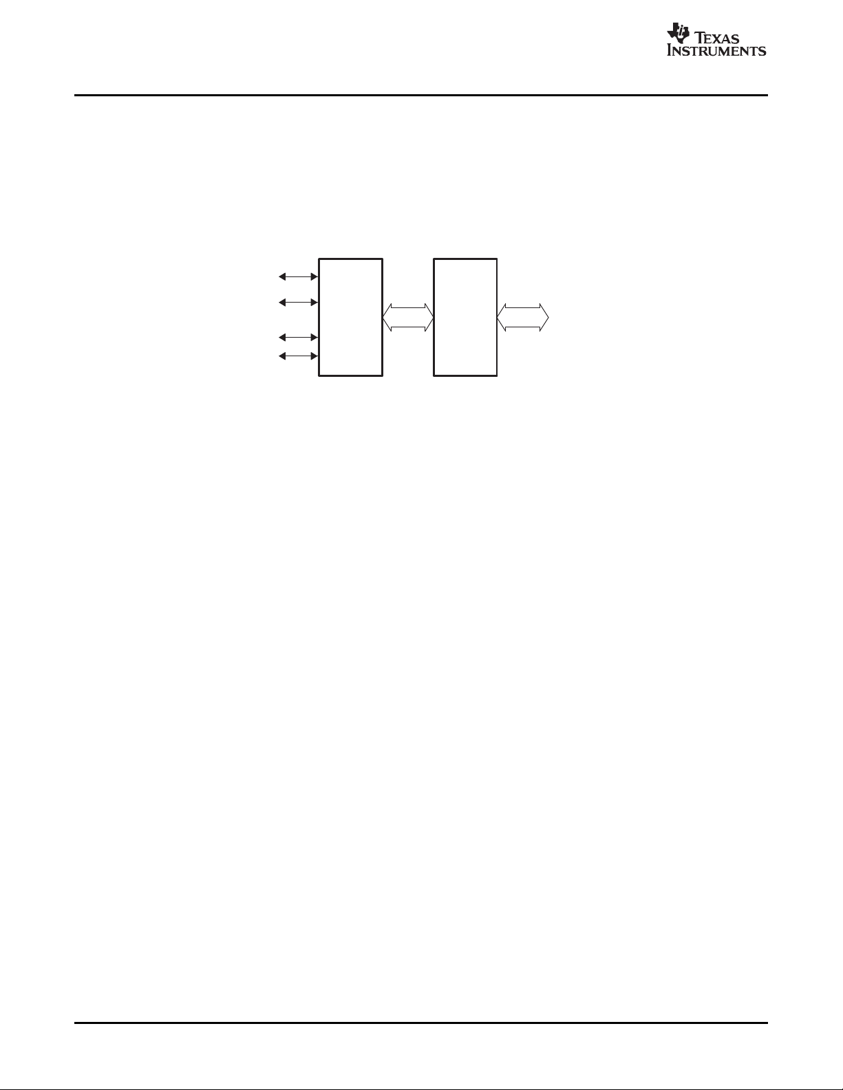
The DDR2 memory controller is the main interface to external DDR2 memory. Figure 1 displays the
general data paths to on-chip peripherals and external DDR2 SDRAM.
Master peripherals, EDMA, the ARM processor, and DSP can access the DDR2 memory controller
through the switched central resource (SCR).
1.4 Supported Use Case Statement
The DDR2 memory controller supports JESD79D-2A DDR2-400 SDRAM memories utilizing either 32-bit
or 16-bit of the DDR2 memory controller data bus. See Section 3 for more details.
Figure 1. Data Paths to DDR2 Memory Controller
1.5 Industry Standard(s) Compliance Statement
The DDR2 memory controller is compliant with the JESD79D-2A DDR2 SDRAM standard with the
exception of the following feature list:
• On Die Termination (ODT). The DDR2 memory controller does not include any on-die terminating
resistors. Furthermore, the on-die terminating resistors of the DDR2 SDRAM device must be disabled
by tying the ODT input pin of the DDR2 SDRAM to ground.
• Differential DQS. The DDR2 memory controller supports single ended DQS signals.
DDR2 Memory Controller8 SPRU986B – November 2007
Submit Documentation Feedback
Page 9
www.ti.com
2 Peripheral Architecture
DDR2
memory
controller
/2
PLLC2
/3
PLLC1
X2_CLKVCLK
DDR_CLK
DDR_CLK
PLL2_SYSCLK1
SYSCLK2
This section describes the architecture of the DDR2 memory controller as well as how it is structured and
how it works within the context of the system-on-a-chip. The DDR2 memory controller can gluelessly
interface to most standard DDR2 SDRAM devices and supports such features as self-refresh mode and
prioritized refresh. In addition, it provides flexibility through programmable parameters such as the refresh
rate, CAS latency, and many SDRAM timing parameters. The following sections include details on how to
interface and properly configure the DDR2 memory controller to perform read and write operations to
externally-connected DDR2 SDRAM devices. Also, Section 3 provides a detailed example of interfacing
the DDR2 memory controller to a common DDR2 SDRAM device.
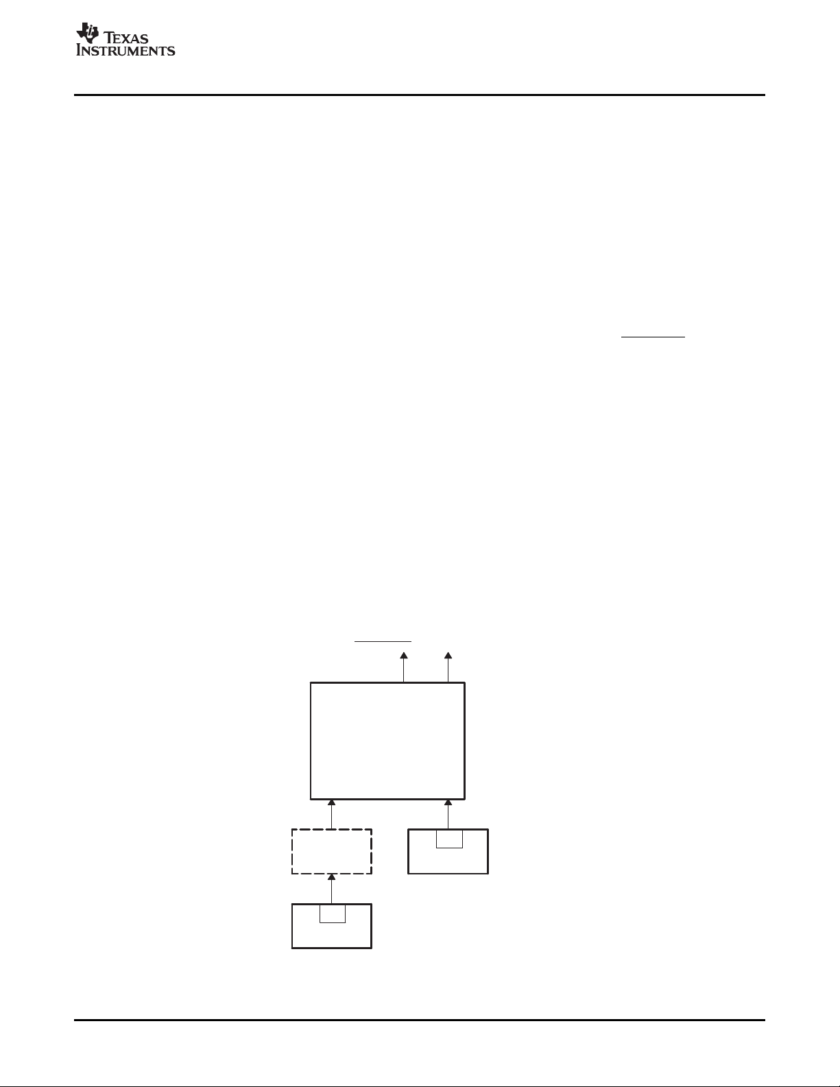
2.1 Clock Control
The DDR2 memory controller receives two input clocks from internal clock sources, SYSCLK2 and
PLL2_SYSCLK1 (Figure 2 ). SYSCLK2 is a divided-down version of the DSP clock. PLL2_SYSCLK1
should be configured to clock at the frequency of the desired data rate, or stated similarly, it should
operate at twice the frequency of the desired DDR2 memory clock. DDR_CLK and DDR_CLK are the two
output clocks of the DDR2 memory controller providing the interface clock to the DDR2 SDRAM memory.
These two clocks operate at a frequency of PLL2_SYSCLK1/2.
2.1.1 Clock Source
SYSCLK2 and PLL2_SYSCLK1 are sourced from two independent PLLs (Figure 2 ). SYSCLK2 is sourced
from PLL controller 1 (PLLC1) and PLL2_SYSCLK1 is sourced from PLL controller 2 (PLLC2).
SYSCLK2 is clocked at a fixed divider ratio of PLL1. This divider is fixed at 3, meaning SYSCLK2 is
clocked at a frequency of PLL1/3. Once inside the DDR2 memory controller, this signal is called VCLK.
PLLC2 has a programmable divider that is used to divide-down the output clock of PLL2. This divider
should be configured such that PLLC2 supplies the PLL2_SYSCLK1 at the desired frequency. For
example, if a 150-MHZ DDR2 interface clock (DDR_CLK) is desired, then PLLC2 must be configured to
generate a 300-MHZ clock on PLL2_SYSCLK1. Once inside the DDR2 memory controller,
PLL2_SYSCLK1 is called X2_CLK.
Peripheral Architecture
Figure 2. DDR2 Memory Controller Clock Block Diagram
SPRU986B – November 2007 DDR2 Memory Controller 9
Submit Documentation Feedback
Page 10

www.ti.com
Peripheral Architecture
2.1.2 Clock Configuration
The frequency of PLL2_SYSCLK1 is configured by selecting the appropriate PLL multiplier and divider
ratio. The PLL multiplier and divider ratio are selected by programming registers within PLLC2. Table 1
shows a list of PLL multiplier and divider settings to achieve certain DDR2 frequencies. The data in
Table 1 is derived by assuming a 27-MHZ reference clock. See the device-specific data manual for the
clock frequencies that are supported. See the TMS320DM643x DMP DSP Subsystem Reference Guide
(SPRU978 ) for information on the PLL controller.
Note: PLLC2 should be configured and a stable clock present on PLL2_SYSCLK1 before releasing
the DDR2 memory controller from reset.
Table 1. PLLC2 Configuration
PLL Multiplier PLL Frequency (MHZ) Divider Ratio X2_CLK Frequency (MHZ) DDR2 Clock Frequency (MHZ)
28 756 3 252 126
19 513 2 256.6 128.3
29 783 3 261 130.5
20 540 2 270 135
31 837 3 279 139.5
21 567 2 283.5 141.8
32 864 3 288 144
22 594 2 297 148.5
23 621 2 310 155.3
24 648 2 324 162
25 675 2 337.5 168.8
2.1.3 DDR2 Memory Controller Internal Clock Domains
There are two clock domains within the DDR2 memory controller. The two clock domains are driven by
VCLK and a divided-down by 2 version of X2_CLK called MCLK. The command FIFO, write FIFO, and
read FIFO described in Section 2.8 are all on the VCLK domain. From this, you can see that VCLK drives
the interface to the peripheral bus.
The MCLK domain consists of the DDR2 memory controller state machine and memory-mapped registers.
This clock domain is clocked at the rate of the external DDR2 memory, X2_CLK/2.
To conserve power within the DDR2 memory controller, VCLK, MCLK, and X2_CLK may be stopped. See
Section 2.16 for proper clock stop procedures.
2.2 Memory Map
See the device-specific data manual for information describing the device memory-map.
DDR2 Memory Controller10 SPRU986B – November 2007
Submit Documentation Feedback
Page 11
www.ti.com
DDR_D[31:0]
DDR2
memory
controller
DDR_CLK
DDR_CLK
DDR_CS
DDR_CKE
DDR_RAS
DDR_WE
DDR_DQM[3:0]
DDR_CAS
DDR_BA[2:0]
DDR_DQS[3:0]
DDR_A[12:0]
DDR_ZN
DDR_ZP
200 Ω
200 Ω
Peripheral Architecture
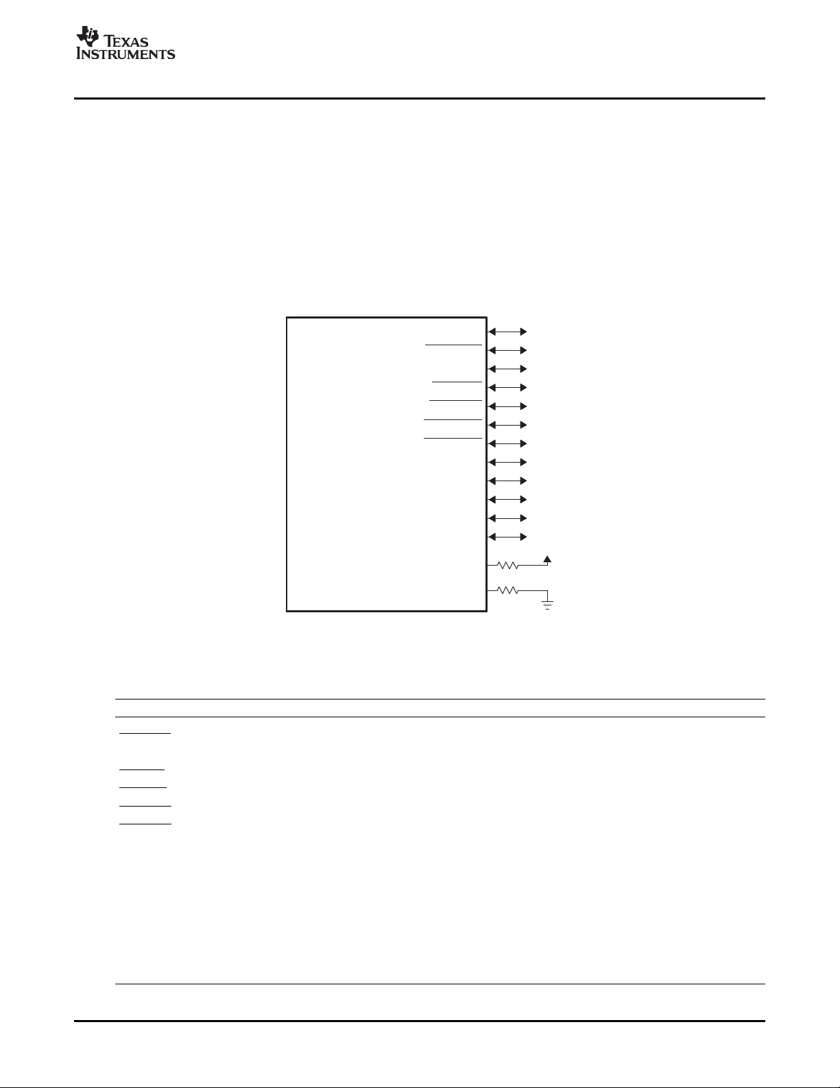
2.3 Signal Descriptions
The DDR2 memory controller signals are shown in Figure 3 and described in Table 2 . The following
features are included:
• The maximum data bus is 32-bits wide.
• The address bus is 13-bits wide with an additional 3 bank address pins.
• Two differential output clocks driven by internal clock sources.
• Command signals: Row and column address strobe, write enable strobe, data strobe, and data mask.
• One chip select signal and one clock enable signal.
Figure 3. DDR2 Memory Controller Signals
Table 2. DDR2 Memory Controller Signal Descriptions
Pin Type Description
DDR_CLK, O/Z Clock: Differential clock outputs.
DDR_CLK
DDR_CKE O/Z Clock enable: Active high.
DDR_CS O/Z Chip select: Active low.
DDR_WE O/Z Write enable strobe: Active low, command output.
DDR_RAS O/Z Row address strobe: Active low, command output.
DDR_CAS O/Z Column address strobe: Active low, command output.
DDR_DQM[3:0] O/Z Data mask: Output mask signal for write data.
DDR_DQS[3:0] I/O/Z Data strobe: Active high, bi-directional signals. Output with write data, input with read data.
DDR_BA[2:0] O/Z Bank address: Output, defining which bank a given command is applied.
DDR_A[12:0] O/Z Address: Address bus.
DDR_D[31:0] I/O/Z Data: Bi-directional data bus. Input for read data, output for write data.
DDR_ZN, O Output impedance control: Required to set the DDR2 output impedance. Connected by way of
DDR_ZP a 200-ohm resistor to power and ground (see Figure 3 ). The resistor should be chosen to be
SPRU986B – November 2007 DDR2 Memory Controller 11
Submit Documentation Feedback
4 times the desired impedance of the output buffer. By changing the size of the resistor, the
DDR2 outputs can be tuned to match the board load, if necessary.
Page 12
www.ti.com
Peripheral Architecture
2.4 Protocol Description(s)
The DDR2 memory controller supports the DDR2 SDRAM commands listed in Table 3 . Table 4 shows the
signal truth table for the DDR2 SDRAM commands.
Table 3. DDR2 SDRAM Commands
Command Function
ACTV Activates the selected bank and row.
DCAB Precharge all command. Deactivates (precharges) all banks.
DEAC Precharge single command. Deactivates (precharges) a single bank.
DESEL Device Deselect.
EMRS Extended Mode Register set. Allows altering the contents of the mode register.
MRS Mode register set. Allows altering the contents of the mode register.
NOP No operation.
Power Down Power down mode.
READ Inputs the starting column address and begins the read operation.
READ with Inputs the starting column address and begins the read operation. The read operation is followed by a
autoprecharge precharge.
REFR Autorefresh cycle.
SLFREFR Self-refresh mode.
WRT Inputs the starting column address and begins the write operation.
WRT with Inputs the starting column address and begins the write operation. The write operation is followed by a
autoprecharge precharge.
Table 4. Truth Table for DDR2 SDRAM Commands
DDR2
SDRAM: CKE CS RAS CAS WE BA[2:0] A[12:11, 9:0] A10
DDR2
memory
controller: DDR_CKE DDR_CS DDR_RAS DDR_CAS DDR_WE DDR_BA[2:0] DDR_A[12:11, 9:0] DDR_A[10]
Previous
Cycles Current Cycle
ACTV H H L L H H Bank Row Address
DCAB H H L L H L X X L
DEAC H H L L H L Bank X L
MRS H H L L L L BA OP Code
EMRS H H L L L L BA OP Code
READ H H L H L H BA Column Address L
READ with H H L H L H BA Column Address H
precharge
WRT H H L H L L BA Column Address L
WRT with H H L H L L BA Column Address L
precharge
REFR H H L L L H X X X
SLFREFR H L L L L H X X X
entry
SLFREFR L H H X X X X X X
exit
NOP H X L H H H X X X
DESEL H X H X X X X X X
Power Down H L H X X X X X X
entry
Power Down L H H X X X X X X
exit
L H H H X X X
L H H H X X X
L H H H X X X
12 DDR2 Memory Controller SPRU986B – November 2007
Submit Documentation Feedback
Page 13

www.ti.com
2.4.1 Refresh Mode
DDR_CLK
DDR_CKE
DDR_CS
DDR_RAS
DDR_CAS
DDR_WE
DDR_A[12:0]
DDR_BA[2:0]
DDR_DQM[3:0]
RFR
DDR_CLK
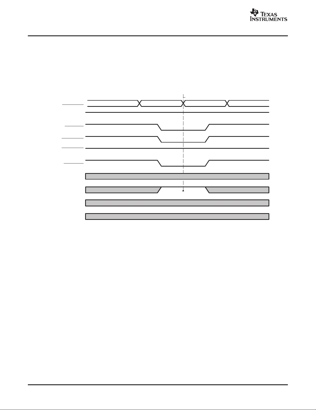
The DDR2 memory controller issues refresh commands to the DDR2 SDRAM memory (Figure 4 ). REFR
is automatically preceded by a DCAB command, ensuring the deactivation of all CE spaces and banks
selected. Following the DCAB command, the DDR2 memory controller begins performing refreshes at a
rate defined by the refresh rate (RR) bit in the SDRAM refresh control register (SDRCR). Page information
is always invalid before and after a REFR command; thus, a refresh cycle always forces a page miss. This
type of refresh cycle is often called autorefresh. Autorefresh commands may not be disabled within the
DDR2 memory controller. See Section 2.9 for more details on REFR command scheduling.
Peripheral Architecture
Figure 4. Refresh Command
SPRU986B – November 2007 DDR2 Memory Controller 13
Submit Documentation Feedback
Page 14
www.ti.com
DDR_CLK
DDR_CKE
DDR_CS
DDR_RAS
DDR_WE
DDR_A[12,11, 9:0]
DDR_BA[2:0]
DDR_DQM[3:0]
DCAB
DDR_A[10]
DDR_CAS
DDR_CLK
Peripheral Architecture
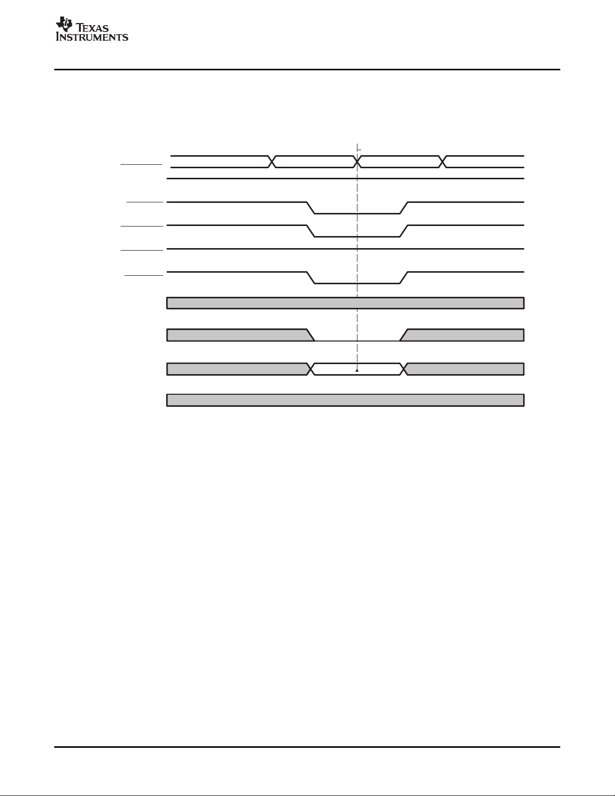
2.4.2 Deactivation (DCAB and DEAC)
The precharge all banks command (DCAB) is performed after a reset to the DDR2 memory controller or
following the initialization sequence. DDR2 SDRAMs also require this cycle prior to a refresh (REFR) and
mode set register commands (MRS and EMRS). During a DCAB command, DDR_A[10] is driven high to
ensure the deactivation of all banks. Figure 5 shows the timing diagram for a DCAB command.
Figure 5. DCAB Command
14 DDR2 Memory Controller SPRU986B – November 2007
Submit Documentation Feedback
Page 15
www.ti.com
DDR_CLK
DDR_CKE
DDR_CS
DDR_RAS
DDR_WE
DDR_A[12,11, 9:0]
DDR_BA[2:0]
DDR_DQM[3:0]
DEAC
DDR_A[10]
DDR_CAS
DDR_CLK
Peripheral Architecture
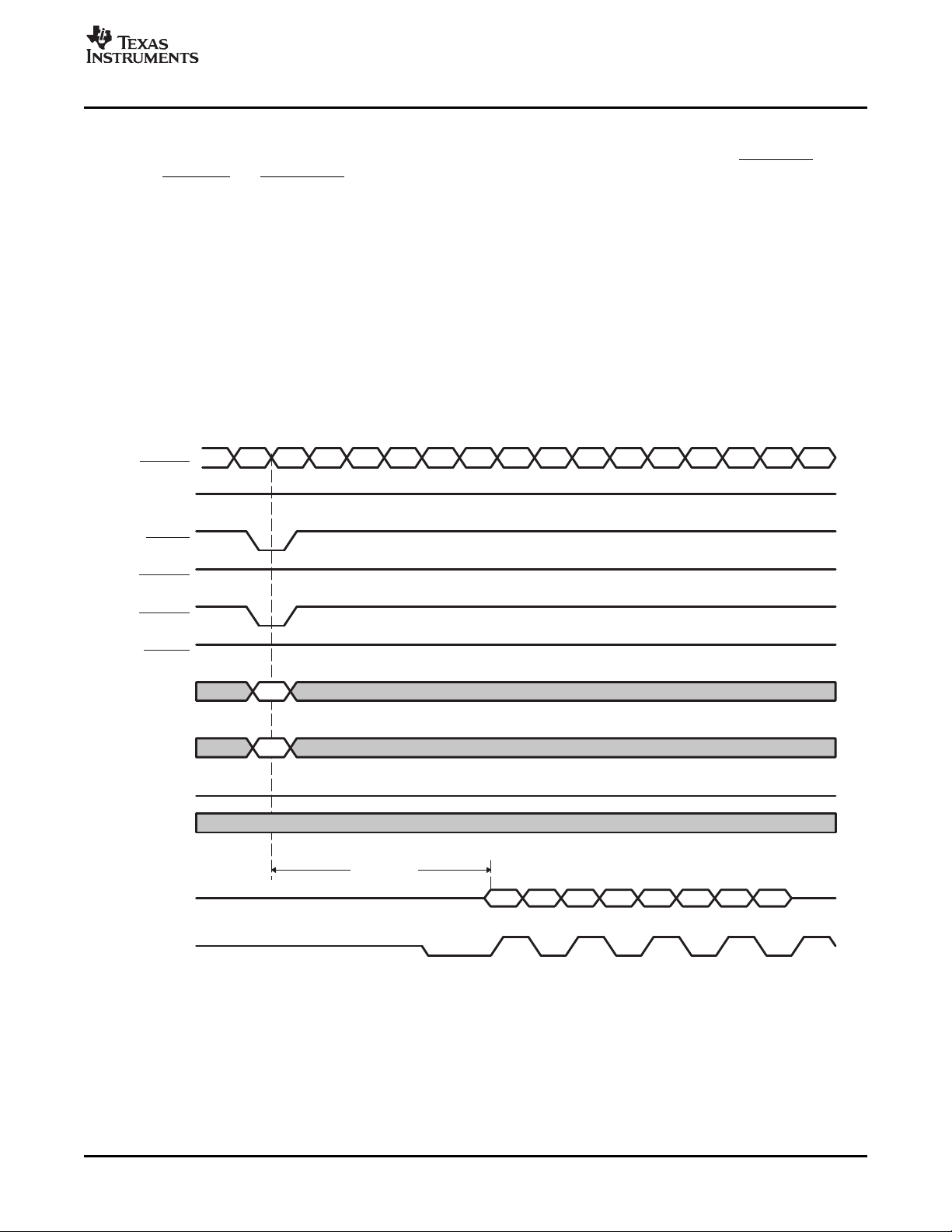
The DEAC command closes a single bank of memory specified by the bank select signals. Figure 6 shows
the timings diagram for a DEAC command.
Figure 6. DEAC Command
SPRU986B – November 2007 DDR2 Memory Controller 15
Submit Documentation Feedback
Page 16

www.ti.com
DDR_CLK
DDR_CKE
DDR_CS
DDR_RAS
DDR_WE
DDR_BA[2:0]
DDR_DQM[3:0]
ACTV
DDR_A[12:0]
DDR_CAS
BANK
ROW
DDR_CLK
Peripheral Architecture
2.4.3 Activation (ACTV)
The DDR2 memory controller automatically issues the activate (ACTV) command before a read or write to
a closed row of memory. The ACTV command opens a row of memory, allowing future accesses (reads or
writes) with minimum latency. The value of DDR_BA[2:0] selects the bank and the value of A[12:0] selects
the row. When the DDR2 memory controller issues an ACTV command, a delay of t
a read or write command is issued. Figure 7 shows an example of an ACTV command. Reads or writes to
the currently active row and bank of memory can achieve much higher throughput than reads or writes to
random areas because every time a new row is accessed, the ACTV command must be issued and a
delay of t
is incurred before
RCD
incurred.
RCD
Figure 7. ACTV Command
DDR2 Memory Controller16 SPRU986B – November 2007
Submit Documentation Feedback
Page 17
www.ti.com
2.4.4 READ Command
DDR_CLK
DDR_CKE
DDR_CS
DDR_WE
DDR_CAS
DDR_DQM[3:0]
DDR_D[31:0]
DDR_A[12:0]
DDR_RAS
DDR_DQS[3:0]
COL
BANK
DDR_A[10]
DDR_BA[2:0]
CAS Latency
D0 D1 D2 D3 D4 D5 D6 D7
DDR_CLK
Peripheral Architecture
Figure 8 shows the DDR2 memory controller performing a read burst from DDR2 SDRAM. The READ
command initiates a burst read operation to an active row. During the READ command, DDR_CAS drives
low, DDR_WE and DDR_RAS remain high, the column address is driven on DDR_A[12:0], and the bank
address is driven on DDR_BA[2:0].
The DDR2 memory controller uses a burst length of 8, and has a programmable CAS latency of 2, 3, 4, or
5. The CAS latency is three cycles in Figure 8 . Read latency is equal to CAS latency plus additive latency.
The DDR2 memory controller always configures the memory to have an additive latency of 0, so read
latency equals CAS latency. Since the default burst size is 8, the DDR2 memory controller returns 8
pieces of data for every read command. If additional accesses are not pending to the DDR2 memory
controller, the read burst completes and the unneeded data is disregarded. If additional accesses are
pending, depending on the scheduling result, the DDR2 memory controller can terminate the read burst
and start a new read burst. Furthermore, the DDR2 memory controller does not issue a DAB/DEAC
command until page information becomes invalid.
Figure 8. DDR2 READ Command
SPRU986B – November 2007 DDR2 Memory Controller 17
Submit Documentation Feedback
Page 18

www.ti.com
DDR_CLK
DDR_CKE
DDR_CS
DDR_WE
DDR_CAS
DDR_DQM[3:0]
DDR_D[31:0]
DDR_A[12:0]
DDR_RAS
DDR_DQS[3:0]
COL
BANK
DDR_A[10]
DDR_BA[2:0]
DQM7
Sample
D0 D1 D2 D3 D4 D5 D6 D7
DQM1 DQM2 DQM3 DQM4 DQM5 DQM6 DQM8
Write Latency
DDR_CLK
Peripheral Architecture
2.4.5 Write (WRT) Command
Prior to a WRT command, the desired bank and row are activated by the ACTV command. Following the
WRT command, a write latency is incurred. Write latency is equal to CAS latency minus 1. All writes have
a burst length of 8. The use of the DDR_DQM outputs allows byte and halfword writes to be executed.
Figure 9 shows the timing for a write on the DDR2 memory controller.
If the transfer request is for less than 8 words, depending on the scheduling result and the pending
commands, the DDR2 memory controller can:
• Mask out the additional data using DDR_DQM outputs
• Terminate the write burst and start a new write burst
The DDR2 memory controller does not perform the DEAC command until page information becomes
invalid.
Figure 9. DDR2 WRT Command
DDR2 Memory Controller18 SPRU986B – November 2007
Submit Documentation Feedback
Page 19

www.ti.com
2.4.6 Mode Register Set (MRS and EMRS)
DDR_CLK
DDR_CKE
DDR_CS
DDR_RAS
DDR_WE
DDR_BA[2:0]
COL
MRS/EMRS
DDR_A[12:0]
DDR_CAS
BANK
DDR_CLK
DDR2 SDRAM contains mode and extended mode registers that configure the DDR2 memory for
operation. These registers control burst type, burst length, CAS latency, DLL enable/disable (on DDR2
device), single-ended strobe, etc.
The DDR2 memory controller programs the mode and extended mode registers of the DDR2 memory by
issuing MRS and EMRS commands. When the MRS or EMRS command is executed, the value on
DDR_BA[1:0] selects the mode register to be written and the data on DDR_A[12:0] is loaded into the
register. Figure 10 shows the timing for an MRS and EMRS command.
The DDR2 memory controller only issues MRS and EMRS commands during the DDR2 memory controller
initialization sequence. See Section 2.13 for more information.
Peripheral Architecture
Figure 10. DDR2 MRS and EMRS Command
SPRU986B – November 2007 DDR2 Memory Controller 19
Submit Documentation Feedback
Page 20

www.ti.com
DDR2 memory controller data bus
DDR_D[31:24]
DDR_D[23:16] DDR_D[15:8] DDR_D[7:0]
32-bit memory device
16-bit memory device
Peripheral Architecture
2.5 Memory Width and Byte Alignment
The DDR2 memory controller supports memory widths of 16 bits and 32 bits. Table 5 summarizes the
addressable memory ranges on the DDR2 memory controller. See the device-specific data manual for the
memory widths that are supported.
Figure 11 shows the byte lanes used on the DDR2 memory controller. The external memory is always
right-aligned on the data bus.
Memory Width Maximum addressable bytes per CS space Description
× 16 128 Mbytes Halfword address
× 32 256 Mbytes Word address
Table 5. Addressable Memory Ranges
Figure 11. Byte Alignment
DDR2 Memory Controller20 SPRU986B – November 2007
Submit Documentation Feedback
Page 21

www.ti.com
2.6 Endianness Considerations
Peripheral Architecture
The DDR2 memory controller supports little-endian operating mode. This determines the order in which
data on the internal data bus is written to or read from devices that are not as wide as the internal data
bus. However, the DDR2 memory controller maintains the natural order of endian operations. That is, a
stream of data starting at any address N will always be accessed in the correct or incrementing data
order. The DDR2 memory controller will always access address N prior to N + 1 in any data width. Table 6
and Table 7 show operation of the DDR2 memory controller for both 16-bit and 32-bit external memory.
See the device-specific data manual for the memory widths that are supported.
Table 6. 16-Bit External Memory
Internal Data (64-Bit DDR_A[2:1] DDR_D[15:0]
0123 4567 89AB CDEFh 00 CDEFh
0123 4567 89AB CDEFh 01 89ABh
0123 4567 89AB CDEFh 10 4567h
0123 4567 89AB CDEFh 11 0123h
Table 7. 32-Bit External Memory
Internal Data (64-Bit) DDR_A[2] DDR_D[31:0]
0123 4567 89AB CDEFh 0 89AB CDEFh
0123 4567 89AB CDEFh 1 0123 4567h
SPRU986B – November 2007 DDR2 Memory Controller 21
Submit Documentation Feedback
Page 22

www.ti.com
Peripheral Architecture
2.7 Address Mapping
The DDR2 memory controller views external DDR2 SDRAM as one continuous block of memory. This
statement is true regardless of the number of external physical devices mapped to a given chip select
space. The DDR2 memory controller receives DDR2 memory access requests along with a 32-bit logical
address from the rest of the system. In turn, the DDR2 memory controller uses the logical address to
generate a row/page, column, and bank address for the DDR2 SDRAM. The number of column and bank
address bits used is determined by the IBANK and PAGESIZE fields in the SDRAM bank configuration
register (SDBCR) (see Table 8 ).
Table 8. Bank Configuration Register Fields for Address Mapping
Bit Field Bit Value Bit Description
IBANK Defines the number of internal banks on the external DDR2 memory.
0 1 bank
1h 2 banks
2h 4 banks
3h 8 banks
PAGESIZE Defines the page size of each page of the external DDR2 memory.
0 256 words (requires 8 column address bits)
1h 512 words (requires 9 column address bits)
2h 1024 words (requires 10 column address bits)
3h 2048 words (requires 11 column address bits)
As stated in Table 8 , the IBANK and PAGESIZE fields of SDBCR control the mapping of the logical,
source address of the DDR2 memory controller to the DDR2 SDRAM row, column, and bank address bits.
The DDR2 memory controller logical address always contains 13 row address bits, whereas the number of
column and bank bits are determined by the IBANK and PAGESIZE fields. Table 9 and Table 10 show
how the logical address bits map to the DDR2 SDRAM row, column, and bank bits for combinations of
IBANK and PAGESIZE values. The same DDR2 memory controller pins provide the row and column
address to the DDR2 SDRAM, thus the DDR2 memory controller appropriately shifts the address during
row and column address selection.
Figure 12 shows how this address-mapping scheme organizes the DDR2 SDRAM rows, columns, and
banks into the device memory map. Note that during a linear access, the DDR2 memory controller
increments the column address as the logical address increments. When the DDR2 memory controller
reaches a page/row boundary, it moves onto the same page/row in the next bank. This movement
continues until the same page has been accessed in all banks. To the DDR2 SDRAM, this process looks
as shown in Figure 13 .
By traversing across banks while remaining on the same row/page, the DDR2 memory controller
maximizes the number of activated banks for a linear access. This results in the maximum number of
open pages when performing a linear access being equal to the number of banks. Note that the DDR2
memory controller never opens more than one page per bank.
Ending the current access is not a condition that forces the active DDR2 SDRAM row to be closed. The
DDR2 memory controller leaves the active row open until it becomes necessary to close it. This decreases
the deactivate-reactivate overhead.
22 DDR2 Memory Controller SPRU986B – November 2007
Submit Documentation Feedback
Page 23

www.ti.com
Peripheral Architecture
Table 9. Logical Address-to-DDR2 SDRAM Address Map for 32-Bit SDRAM
SDBCR Bit Logical Address
IBANK PAGESIZE 31 30 29 28 27 26 25 24 23 22:16 15 14 13 12 11 10 9:2 1:0
0 0 - nrb=13 ncb=8
1 0 - nrb=13 nbb=1 ncb=8
2h 0 - nrb=13 nbb=2 ncb=8
3h 0 - nrb=13 nbb=3 ncb=8
0 1 - nrb=13 ncb=9
1 1 - nrb=13 nbb=1 ncb=9
2h 1 - nrb=13 nbb=2 ncb=9
3h 1 - nrb=13 nbb=3 ncb=9
0 2h - nrb=13 ncb=10
1 2h - nrb=13 nbb=1 ncb=10
2h 2h - nrb=13 nbb=2 ncb=10
3h 2h - nrb=13 nbb=3 ncb=10
0 3h - nrb=13 ncb=11
1 3h - nrb=13 nbb=1 ncb=11
2h 3h - nrb=13 nbb=2 ncb=11
3h 3h nrb=13 nbb=3 ncb=11
(1)
Legend: ncb = number of column address bits; nrb = number of row address bits; nbb = number of bank address bits.
(1)
Table 10. Logical Address-to-DDR2 SDRAM Address Map for 16-bit SDRAM
SDBCR Bit Logical Address
IBANK PAGESIZE 31 30 29 28 27 26 25 24 23 22 21:15 14 13 12 11 10 9 8:1 0
0 0 - nrb=13 ncb=8
1 0 - nrb=13 nbb=1 ncb=8
2h 0 - nrb=13 nbb=2 ncb=8
3h 0 - nrb=13 nbb=3 ncb=8
0 1 - nrb=13 ncb=9
1 1 - nrb=13 nbb=1 ncb=9
2h 1 - nrb=13 nbb=2 ncb=9
3h 1 - nrb=13 nbb=3 ncb=9
0 2h - nrb=13 ncb=10
1 2h - nrb=13 nbb=1 ncb=10
2h 2h - nrb=13 nbb=2 ncb=10
3h 2h - nrb=13 nbb=3 ncb=10
0 3h - nrb=13 ncb=11
1 3h - nrb=13 nbb=1 ncb=11
2h 3h - nrb=13 nbb=2 ncb=11
3h 3h - nrb=13 nbb=3 ncb=11
(1)
Legend: ncb = number of column address bits; nrb = number of row address bits; nbb = number of bank address bits.
(1)
SPRU986B – November 2007 DDR2 Memory Controller 23
Submit Documentation Feedback
Page 24

www.ti.com
Col. 0 Col. 1 Col. 2 Col. 3 Col. 4 Col. M−1 Col. M
Row 0, bank 0
Row 0, bank 1
Row 0, bank 2
Row 0, bank P
Row 1, bank 1
Row 1, bank 0
Row 1, bank 2
Row 1, bank P
Row N, bank 2
Row N, bank 1
Row N, bank 0
Row N, bank P
Peripheral Architecture
Figure 12. Logical Address-to-DDR2 SDRAM Address Map
NOTE: M is number of columns (as determined by PAGESIZE) minus 1, P is number of banks (as determined by
IBANK) minus 1, and N is number of rows (as determined by both PAGESIZE and IBANK) minus 1.
24 DDR2 Memory Controller SPRU986B – November 2007
Submit Documentation Feedback
Page 25

www.ti.com
0 1 2 3 MBank 0
Row 0
Row 1
Row 2
Row N
C
o
l l
C
o
l
C
o
l
C
o
Row 0
Row N
Row 1
Row 2
CC
Bank 1
l l
0 21
oo
C C
l l
3 M
o o
Row 0
Row N
Row 1
Row 2
CC
Bank 2
l l
0 21
oo
llll
Row N
Row 2
Row 0
Row 1
Bank P 0 1 2 3 M
C C
l l
3 M
o o
oCoCoCo
C
Peripheral Architecture
Figure 13. DDR2 SDRAM Column, Row, and Bank Access
NOTE: M is number of columns (as determined by PAGESIZE) minus 1, P is number of banks (as determined by
IBANK) minus 1, and N is number of rows (as determined by both PAGESIZE and IBANK) minus 1.
SPRU986B – November 2007 DDR2 Memory Controller 25
Submit Documentation Feedback
Page 26

www.ti.com
Command/Data
Scheduler
Command FIFO
Write FIFO
Read FIFO
Registers
Command
to Memory
Write Data
to Memory
Read Data
from
Memory
Command
Data
Peripheral Architecture
2.8 DDR2 Memory Controller Interface
To move data efficiently from on-chip resources to external DDR2 SDRAM memory, the DDR2 memory
controller makes use of a command FIFO, a write FIFO, a read FIFO, and command and data schedulers.
Table 11 describes the purpose of each FIFO.
Figure 14 shows the block diagram of the DDR2 memory controller FIFOs. Commands, write data, and
read data arrive at the DDR2 memory controller parallel to each other. The same peripheral bus is used to
write and read data from external memory as well as internal memory-mapped registers.
FIFO Description Depth (64-bit doublewords)
Command Stores all commands coming from on-chip requestors 7
Write Stores write data coming from on-chip requestors to memory 11
Read Stores read data coming from memory to on-chip requestors 17
Table 11. DDR2 Memory Controller FIFO Description
Figure 14. DDR2 Memory Controller FIFO Block Diagram
26 DDR2 Memory Controller SPRU986B – November 2007
Submit Documentation Feedback
Page 27

www.ti.com
2.8.1 Command Ordering and Scheduling, Advanced Concept
The DDR2 memory controller performs command re-ordering and scheduling in an attempt to achieve
efficient transfers with maximum throughput. The goal is to maximize the utilization of the data, address,
and command buses while hiding the overhead of opening and closing DDR2 SDRAM rows. Command
re-ordering takes place within the command FIFO.
Typically, a given master issues commands on a single priority. EDMA transfer controller read and write
ports are different masters. The DDR2 memory controller first reorders commands from each master
based on the following rules:
• Selects the oldest command (first command in the queue)
• Selects a read before a write if:
– The read is to a different block address (2048 bytes) than the write
– The read has greater or equal priority
The second bullet above may be viewed as an exception to the first bullet. This means that for an
individual master, all of its commands will complete from oldest to newest, with the exception that a read
may be advanced ahead of an older, lower or equal priority write. Following this scheduling, each master
may have one command ready for execution.
Next, the DDR2 memory controller examines each of the commands selected by the individual masters
and performs the following reordering:
• Among all pending reads, selects reads to rows already open. Among all pending writes, selects writes
to rows already open.
• Selects the highest priority command from pending reads and writes to open rows. If multiple
commands have the highest priority, then the DDR2 memory controller selects the oldest command.
The DDR2 memory controller may now have a final read and write command. If the Read FIFO is not full,
then the read command will be performed before the write command, otherwise the write command will be
performed first.
Besides commands received from on-chip resources, the DDR2 memory controller also issues refresh
commands. The DDR2 memory controller attempts to delay refresh commands as long as possible to
maximize performance while meeting the SDRAM refresh requirements. As the DDR2 memory controller
issues read, write, and refresh commands to DDR2 SDRAM memory, it adheres to the following rules:
1. Refresh request resulting from the Refresh Must level of urgency being reached
2. Read request without a higher priority write (selected from above reordering algorithm)
3. Refresh request resulting from the Refresh Need level of urgency being reached
4. Write request (selected from above reordering algorithm)
5. Refresh request resulting from Refresh May level of urgency being reached
6. Request to enter self-refresh mode
The following results from the above scheduling algorithm:
• All writes from a single master will complete in order
• All reads from a single master will complete in order
• From the same master, any read to the same location (or within 2048 bytes) as a previous write will
complete in order
Peripheral Architecture
SPRU986B – November 2007 DDR2 Memory Controller 27
Submit Documentation Feedback
Page 28

www.ti.com
Peripheral Architecture
2.8.2 Command Starvation
The reordering and scheduling rules listed above may lead to command starvation, which is the
prevention of certain commands from being processed by the DDR2 memory controller. Command
starvation results from the following conditions:
• A continuous stream of high-priority read commands can block a low-priority write command
• A continuous stream of DDR2 SDRAM commands to a row in an open bank can block commands to
the closed row in the same bank.
To avoid these conditions, the DDR2 memory controller can momentarily raise the priority of the oldest
command in the command FIFO after a set number of transfers have been made. The PR_OLD_COUNT
bit field in the peripheral bus burst priority register (PBBPR) sets the number of the transfers that must be
made before the DDR2 memory controller will raise the priority of the oldest command.
Note: Leaving the PR_OLD_COUNT bits at their default value (FFh) disables this feature of the
2.8.3 Possible Race Condition
A race condition may exist when certain masters write data to the DDR2 memory controller. For example,
if master A passes a software message via a buffer in DDR2 memory and does not wait for indication that
the write completes, when master B attempts to read the software message it may read stale data and
therefore receive an incorrect message. In order to confirm that a write from master A has landed before a
read from master B is performed, master A must wait for the write completion status from the DDR2
memory controller before indicating to master B that the data is ready to be read. If master A does not
wait for indication that a write is complete, it must perform the following workaround:
1. Perform the required write.
2. Perform a dummy write to the DDR2 memory controller SDRAM Status register.
3. Perform a dummy read to the DDR2 memory controller SDRAM Status register.
4. Indicate to master B that the data is ready to be read after completion of the read in step 3. The
completion of the read in step 3 ensures that the previous write was done.
The EDMA and ATA peripherals do not need to implement the above workaround. If a peripheral is not
listed here, then the above workaround is required. Refer to the device-specific data manual for more
information.
EMIF. This means commands can stay in the command FIFO indefinitely. Therefore, these
bits should be set to FEh immediately following reset to enable this feature with the highest
level of allowable memory transfers. It is suggested that system level prioritization be set to
avoid placing high-bandwidth masters on the highest priority levels. These bits can be left as
FEh unless advanced bandwidth/prioritization control is required.
DDR2 Memory Controller28 SPRU986B – November 2007
Submit Documentation Feedback
Page 29

www.ti.com
2.9 Refresh Scheduling
Peripheral Architecture
The DDR2 memory controller issues autorefresh (REFR) commands to DDR2 SDRAM devices at a rate
defined in the refresh rate (RR) bit field in the SDRAM refresh control register (SDRCR). A refresh interval
counter is loaded with the value of the RR bit field and decrements by 1 each cycle until it reaches zero.
Once the interval counter reaches zero, it reloads with the value of the RR bit. Each time the interval
counter expires, a refresh backlog counter increments by 1. Conversely, each time the DDR2 memory
controller performs a REFR command, the backlog counter decrements by 1. This means the refresh
backlog counter records the number of REFR commands the DDR2 memory controller currently has
outstanding.
The DDR2 memory controller issues REFR commands based on the level of urgency. The level of
urgency is defined in Table 12 . Whenever the refresh level of urgency is reached, the DDR2 memory
controller issues a REFR command before servicing any new memory access requests. Following a REFR
command, the DDR2 memory controller waits T_RFC cycles, defined in the SDRAM timing register
(SDTIMR), before rechecking the refresh urgency level.
In addition to the refresh counter previously mentioned, a separate backlog counter ensures the interval
between two REFR commands does not exceed 8 × the refresh rate. This backlog counter increments by 1
each time the interval counter expires and resets to zero when the DDR2 memory controller issues a
REFR command. When this backlog counter is greater than 7, the DDR2 memory controller issues four
REFR commands before servicing any new memory requests.
The refresh counters do not operate when the DDR2 memory is in self-refresh mode.
Table 12. Refresh Urgency Levels
Urgency Level Description
Refresh May Backlog count is greater than 0. Indicates there is a backlog of REFR commands, when the DDR2 memory
controller is not busy it will issue the REFR command.
Refresh Release Backlog count is greater than 3. Indicates the level at which enough REFR commands have been performed
and the DDR2 memory controller may service new memory access requests.
Refresh Need Backlog count is greater than 7. Indicates the DDR2 memory controller should raise the priority level of a
REFR command above servicing a new memory access.
Refresh Must Backlog count is greater than 11. Indicates the level at which the DDR2 memory controller should perform a
REFR command before servicing new memory access requests.
2.10 Self-Refresh Mode
Setting the self refresh (SR) bit in the SDRAM refresh control register (SDRCR) to 1 forces the DDR2
memory controller to place the external DDR2 SDRAM in a low-power mode (self refresh), in which the
DDR2 SDRAM maintains valid data while consuming a minimal amount of power. When the SR bit is
asserted, the DDR2 memory controller continues normal operation until all outstanding memory access
requests have been serviced and the refresh backlog has been cleared. At this point, all open pages of
DDR2 SDRAM are closed and a self-refresh (SLFRFR) command (an autorefresh command with
DDR_CKE low) is issued.
The DDR2 memory controller exits the self-refresh state when a memory access is received or when the
SR bit in SDRCR is cleared to 0. While in the self-refresh state, if a request for a memory access is
received, the DDR2 memory controller services the memory access request, returning to the self-refresh
state upon completion. The DDR2 memory controller will not wake up from the self-refresh state (whether
from a memory access request or from clearing the SR bit) until T_CKE + 1 cycles have expired since the
self-refresh command was issued. The value of T_CKE is defined in the SDRAM timing 2 register
(SDTIMR2).
After exiting from the self-refresh state, the DDR2 memory controller will not immediately start executing
commands. Instead, it will wait T_SXNR + 1 clock cycles before issuing non-read commands and
T_SXRD + 1 clock cycles before issuing read commands. The SDRAM timing 2 register (SDTIM2)
programs the values of T_SXNR and T_SXRD.
SPRU986B – November 2007 DDR2 Memory Controller 29
Submit Documentation Feedback
Page 30

www.ti.com
DDR2
memory
controller
registers
Hard
Reset from
PLLC1
State
machine
VRST
VCTL_RST
DDR
PSC
Peripheral Architecture
Once in self-refresh mode, the DDR2 memory controller input clocks (VCLK and X2_CLK) may be gated
off or changed in frequency. Stable clocks must be present before exiting self-refresh mode. See
Section 2.16 for more information describing the proper procedure to follow when shutting down DDR2
memory controller input clocks.
2.11 Reset Considerations
The DDR2 memory controller has two reset signals, VRST and VCTL_RST. The VRST is a module-level
reset that resets both the state machine as well as the DDR2 memory controller memory-mapped
registers. The VCTL_RST resets the state machine only. If the DDR2 memory controller is reset
independently of other peripherals, the user's software should not perform memory, as well as register
accesses, while VRST or VCTL_RST are asserted. If memory or register accesses are performed while
the DDR2 memory controller is in the reset state, other masters may hang. Following the rising edge of
VRST or VCTL_RST, the DDR2 memory controller immediately begins its initialization sequence.
Command and data stored in the DDR2 memory controller FIFOs are lost. Table 13 describes the different
methods for asserting each reset signal. The Power and Sleep Controller (PSC) acts as a master
controller for power management for all of the peripherals on the device. For detailed information on
power management procedures using the PSC, see the TMS320DM643x DMP DSP Subsystem
Reference Guide (SPRU978 ). Figure 15 shows the DDR2 memory controller reset diagram.
Table 13. Reset Sources
Reset Signal Reset Source
VRST Hardware/device reset
VCTL_RST Power and sleep controller
Figure 15. DDR2 Memory Controller Reset Block Diagram
DDR2 Memory Controller30 SPRU986B – November 2007
Submit Documentation Feedback
Page 31

www.ti.com
2.12 VTP IO Buffer Calibration
The DDR2 memory controller is able to control the impedance of the output IO. This feature allows the
DDR2 memory controller to tune the output impedance of the IO to match that of the PCB board. Control
of the output impedance of the IO is an important feature because impedance matching reduces
reflections, creating a cleaner board design. Calibrating the output impedance of the IO will also reduce
the power consumption of the DDR2 memory controller. The calibration is performed with respect to
voltage, temperature, and process (VTP). The VTP information obtained from the calibration is used to
control the output impedance of the IO.
The impedance of the output IO is selected by the value of resistors connected to the DDR_ZN and
DDR_ZP pins. The resistor should be chosen to be 4 times the desired impedance of the output IO. The
DDR2 reference design requires the resistor values to be 200 ohms. This means that both the DDR_ZN
and DDR_ZP pins must have a 200 ohm resistor connected to them. Figure 3 describes proper
connection of the DDR_ZN and DDR_ZP pins.
To set the output impedance of the IO, calibration must be initiated by writing to the following
memory-mapped registers:
• VTP IO Control Register (VTPIOCR)
• DDR VTP Register (DDRVTPR)
• DDR VTP Enable Register (DDRVTPER)
The VTP IO control register is written to begin the calibration. Once the calibration is complete, the VTP
information is stored in the DDR VTP register. The DDR VTP register should then be read, retrieving the
VTP information, and the VTP information written to the VTP IO control register. The DDR VTP enable
register is written to enable/disable access to the DDR VTP register. Steps 8-15 of the initialization
procedure described in Section 2.13.2 shows the procedure that must be followed to perform VTP IO
calibration.
Peripheral Architecture
Note: VTP IO calibration must be performed following device power up and device reset. If the
2.13 Auto-Initialization Sequence
The DDR2 SDRAM contains mode and extended mode registers that configure the DDR2 memory for
operation. These registers control burst type, burst length, CAS latency, DLL enable/disable (on the DDR2
device), single-ended strobe, etc. The DDR2 memory controller programs the mode and extended mode
registers of the DDR2 memory by issuing MRS and EMRS commands during the initialization sequence.
The initialization sequence performed by the DDR2 memory controller is compliant with the JESDEC79-2A
specification. The DDR2 memory controller performs an initialization sequence under the following
conditions:
• Following reset (rising edge of VRST or VCTL_RST)
• Following a write to the DDRDRIVE bit field or the two least-significant bytes in the SDRAM bank
configuration register (SDBCR)
During the initialization sequence, the DDR2 memory controller issues MRS and EMRS commands that
configure the DDR2 SDRAM mode register and extended mode register 1 with the values described in
Table 14 and Table 15 . The DDR2 SDRAM extended mode registers 2 and 3 are configured with a value
of 0h. At the end of the initialization sequence, the DDR2 memory controller performs an autorefresh
cycle, leaving the DDR2 memory controller in an idle state with all banks deactivated.
When a reset occurs, the DDR2 memory controller immediately begins the initialization sequence. Under
this condition, commands and data stored in the DDR2 memory controller FIFOs will be lost. However,
when the initialization sequence is initiated by a write to the two least-significant bytes in SDBCR, data
and commands stored in the DDR2 memory controller FIFOs will not be lost and the DDR2 memory
controller will ensure read and write commands are completed before starting the initialization sequence.
DDR2 memory controller is reset via the Power and Sleep Controller (PSC) and the VTP
input clock is disabled, accesses to the DDR2 memory controller will not complete. To
re-enable accesses to the DDR2 memory controller, enable the VTP input clock and then
perform the VTP calibration sequence again.
SPRU986B – November 2007 DDR2 Memory Controller 31
Submit Documentation Feedback
Page 32

www.ti.com
Peripheral Architecture
Table 14. DDR2 SDRAM Configuration by MRS Command
DDR2 Memory
Controller DDR2 SDRAM
Address Bus Value Register Bit DDR2 SDRAM Field Function Selection
DDR_A[12] 0 12 Power Down Exit Fast exit
DDR_A[11:9] t_WR 11:9 Write Recovery Write recovery from autoprecharge. Value of 2,
DDR_A[8] 0 8 DLL Reset Out of reset
DDR_A[7] 0 7 Mode: Test or Normal Normal mode
DDR_A[6:4] CL bit 6:4 CAS Latency Value of 2, 3, 4, or 5 is programmed based on
DDR_A[3] 0 3 Burst Type Sequential
DDR_A[2:0] 3h 2:0 Burst Length 8
3, 4, 5, or 6 is programmed based on value of
the T_WR bit in the SDRAM timing register
(SDTIMR).
value of the CL bit in the SDRAM bank
configuration register (SDBCR).
Table 15. DDR2 SDRAM Configuration by EMRS(1) Command
DDR2 Memory
Controller DDR2 SDRAM
Address Bus Value Register Bit DDR2 SDRAM Field Function Selection
DDR_A[12] 0 12 Output Buffer Enable Output buffer enable
DDR_A[11] 0 11 RDQS Enable RDQS disable
DDR_A[10] 1 10 DQS enable Disables differential DQS signaling.
DDR_A[9:7] 0 9:7 OCD Calibration Program Exit OCD calibration
DDR_A[6] 0 6 ODT Value (Rtt) Cleared to 0 to select 75 ohms. This feature is
DDR_A[5:3] 0 5:3 Additive Latency 0 cycles of additive latency
DDR_A[2] 1 2 ODT Value (Rtt) Set to 1 to select 75 ohms. This feature is not
DDR_A[1] 1 1 Output Driver Impedance DDR2 drive strength programmed to weak
DDR_A[0] 0 0 DLL enable DLL enable
not supported because the DDR_ODT signal is
not pinned out.
supported because the DDR_ODT signal is not
pinned out.
(60%).
2.13.1 Initializing Configuration Registers
Perform the following steps when configuring the DDR2 memory controller memory-mapped registers:
1. Program the DDR PHY control register (DDRPHYCR) by setting the read latency (READLAT) bits to
the desired value as well as clearing the DLLPWRDN bit to 0.
2. Program the SDRAM bank configuration register (SDBCR) to the desired value with the TIMUNLOCK
bit set to 1 (unlocked).
3. Program the SDRAM timing register (SDTIMR) and SDRAM timing register 2 (SDTIMR2) to the
desired values to meet the DDR2 SDRAM memory data sheet specification.
4. Program SDBCR to the desired value with the TIMUNLOCK bit cleared to 0 (locked).
5. Program the RR bit in the SDRAM refresh control register (SDRCR) to the desired value to meet the
refresh requirements of the DDR2 SDRAM memory.
DDR2 Memory Controller32 SPRU986B – November 2007
Submit Documentation Feedback
Page 33

www.ti.com
2.13.2 Initializing Following Device Power Up and Device RESET
The following power-up sequence is preliminary and is documented to
reflect the intended-use case. This power-up sequence may change at a
future date.
Following device power up, the DDR2 memory controller is held in reset with the internal clocks to the
module gated off. Before releasing the DDR2 memory controller from reset, the clocks to the module must
be turned on. Perform the following steps when turning the clocks on and initializing the module:
1. Program PLLC2 registers to provide a stable clock on PLL2_SYSCLK1 at the desired frequency.
2. Program the DDR2 memory controller Power and Sleep Controller (PSC) to enable VCLK.
3. Follow the register initialization procedure described in Section 2.13.1 to complete the DDR2 memory
controller configuration.
4. Perform a dummy read of DDR2 memory to verify initialization sequence has completed.
5. Perform a soft reset of the DDR2 memory controller via the PSC using the following procedure. See
the TMS320DM643x DMP DSP Subsystem Reference Guide (SPRU978 ) for details on how to
program the PSC.
a. To put the DDR2 memory controller into soft reset, program the PSC to place the DDR2 memory
controller into the SyncReset state.
b. To take the DDR2 memory controller out of soft reset, program the PSC to place the DDR2
memory controller into the Enable state.
6. Enable VTP manual calibration by writing to the VTP IO control register (VTPIOCR). See Section 4.12
for details on VTPIOCR.
a. With a single write, set the EN bit field (bit 13) to 1 and the RECAL bit field (bit 15) to 0 by writing a
value of 0000 201Fh.
b. Set the RECAL bit field (bit 15) to 1, making sure the value written to the EN field is still 1 by writing
a value of 0000 A01Fh. This begins the calibration sequence.
7. Wait for a minimum of 33 VTP clk cycles for calibration to complete. The VTP clock operates at
13.5 MHZ.
8. Enable access to the DDR VTP register by writing a 1 to the DDR VTP enable register.
9. Read the DDR VTP register to get the P/N channel VTP value. See Section 4.13 for details on the
DDR VTP register.
10. Write the VTP information to the PCH and NCH fields in the VTPIOCR. Make sure the RECAL and EN
bits remain set to 1.
11. Write 0 to EN bit field in the VTP control register to disable VTP calibration.
12. Disable access to the DDR VTP register by writing a 0 to the DDR VTP enable register.
13. Disable VTP input clock by disabling the bypass clock of PLL2.
Peripheral Architecture
CAUTION
Note: If the DDR2 memory controller is reset via the Power and Sleep Controller (PSC) and the
VTP input clock is disabled, accesses to the DDR2 memory controller will not complete. To
re-enable accesses to the DDR2 memory controller, enable the VTP input clock and then
perform the VTP calibration sequence again.
SPRU986B – November 2007 DDR2 Memory Controller 33
Submit Documentation Feedback
Page 34

www.ti.com
PLLC2
CLKSTOP_REQ
DDR
PSC
CLKSTOP_ACK
MODCLK
MODRST
LRST
DDR2
memory
controller
VCLKSTOP_REQ
VCLKSTOP_ACK
VCLK
VRST
VCTL_RST
X2_CLK
/2
SYSCLK2
PLL2_SYSCLK1
Peripheral Architecture
2.14 Interrupt Support
The DDR2 memory controller supports two addressing modes, linear incrementing and cache line wrap.
Upon receipt of an access request for an unsupported addressing mode, the DDR2 memory controller
generates an interrupt by setting the LT bit in the interrupt raw register (IRR). The DDR2 memory
controller will then treat the request as a linear incrementing request.
This interrupt is called the line trap interrupt and is the only interrupt the DDR2 memory controller
supports. It is an active-high interrupt and is enabled by the LTMSET bit in the interrupt mask set register
(IMSR). This interrupt is mapped to both the DSP and the ARM and is not multiplexed with other
interrupts.
2.15 DMA Event Support
The DDR2 memory controller is a DMA slave peripheral and therefore does not generate DMA events.
Data read and write requests may be made directly by masters and by the DMA.
2.16 Power Management
Power dissipation from the DDR2 memory controller may be managed by two methods:
• Self-refresh mode (see Section 2.10 )
• Gating input clocks to the module off
Gating input clocks off to the DDR2 memory controller achieves higher power savings when compared to
the power savings of self-refresh mode. The input clocks are turned off outside of the DDR2 memory
controller through the use of the Power and Sleep Controller (PSC) and the PLL controller 2 (PLLC2).
Figure 16 shows the connections between the DDR2 memory controller, PSC, and PLLC2. For detailed
information on power management procedures using the PSC, see the TMS320DM643x DMP DSP
Subsystem Reference Guide (SPRU978 ).
Before gating clocks off, the DDR2 memory controller must place the DDR2 SDRAM memory in
self-refresh mode by setting the SR bit in the SDRAM refresh control register (SDRCR) to 1. If the external
memory requires a continuous clock, the DDR2 memory controller clock provided by PLLC2 must not be
turned off because this may result in data corruption. See the following subsections for the proper
procedures to follow when stopping the DDR2 memory controller clocks. Once the clocks are stopped, to
re-enable the clocks follow the clock stop procedure in each respective subsection in reverse order.
Figure 16. DDR2 Memory Controller Power Sleep Controller Diagram
DDR2 Memory Controller34 SPRU986B – November 2007
Submit Documentation Feedback
Page 35

www.ti.com
2.16.1 DDR2 Memory Controller Clock Stop Procedure
The following clock stop procedures are preliminary and are documented
to reflect the intended-use cases. These clock stop procedures may
change at a future date.
Note: If an access occurs to the DDR2 memory controller after completing steps 1-5, the DLL will
wake up and lock, then the MCLK will turn on and the access will be performed. Following
step 6, all DDR2 accesses are disabled until the DDR2 memory controller is enabled again
through the LPSC.
To achieve maximum power savings VCLK, MCLK, X2_CLK, DDR_CLK, and DDR_CLK should be gated
off, as well as the DDR2 memory controller DLL powered down. Perform the following procedure when
shutting down clocks to achieve maximum power savings:
1. Allow software to complete the desired DDR2 transfers.
2. Set the SR bit in the DDR2 SDRAM refresh control register (SDRCR). The DDR2 memory controller
will complete any outstanding accesses and backlogged refresh cycles and then place the external
DDR2 memory in self-refresh mode.
3. Set the MCLKSTOPEN bit in SDRCR. This enables the DDR2 memory controller to shut off the MCLK.
4. Set the DLLPWRDN bit in the DDR PHY control register (DDRPHYCR) to 1 to power down the DDR2
memory controller DLL.
5. Poll the PHYRDY bit in the SDRAM status register (SDRSTAT) to be a logic-low indicating that the
MCLK has been stopped and the DLL is powered down.
6. Program DDR2 memory controller LPSC to disable VCLK.
7. Program PLLC2 registers to stop PLL2_SYSCLK1 which disables X2_CLK of the DDR2 memory
controller, as well as DDR_CLK and DDR_CLK.
To turn clocks back on:
1. Program PLLC2 registers to start PLL2_SYSCLK1 which sources X2_CLK of the DDR2 memory
controller.
2. Once PLL2_SYSCLK1 is stable, program the DDR2 memory controller LPSC to enable VCLK.
3. Clear the MCLKSTOPEN bit in the DDR2 SDRAM refresh control register (SDRCR) to 0.
4. Clear the DLLPWRDN bit in the DDR PHY control register (DDRPHYCR) to 0 to power up the DDR2
memory controller DLL.
5. Perform a soft reset of the DDR2 memory controller via the PSC using the following procedure. See
the TMS320DM643x DMP DSP Subsystem Reference Guide (SPRU978 ) for details on how to
program the PSC.
a. To put the DDR2 memory controller into soft reset, program the PSC to place the DDR2 memory
controller into the SyncReset state.
b. To take the DDR2 memory controller out of soft reset, program the PSC to place the DDR2
memory controller into the Enable state.
6. Clear the SR bit in SDRCR to 0.
Peripheral Architecture
CAUTION
2.17 Emulation Considerations
The DDR2 memory controller will remain fully functional during emulation halts to allow emulation access
to external memory.
SPRU986B – November 2007 DDR2 Memory Controller 35
Submit Documentation Feedback
Page 36

www.ti.com
Supported Use Cases
3 Supported Use Cases
The DDR2 memory controller allows a high degree of programmability for shaping DDR2 accesses. The
programmability inherent to the DDR2 memory controller provides the DDR2 memory controller with the
flexibility to interface with a variety of DDR2 devices. By programming the SDRAM bank configuration
register (SDBCR), SDRAM refresh control register (SDRCR), SDRAM timing register (SDTIMR), and
SDRAM timing register 2 (SDTIMR2), the DDR2 memory controller can be configured to meet the data
sheet specification for JESD79D-2A compliant DDR2 SDRAM.
This section presents an example describing how to interface the DDR2 memory controller to a JESD79D
DDR2-400 1-Gb device. The DDR2 memory controller is assumed to be operating at 133 MHZ.
3.1 Connecting the DDR2 Memory Controller to DDR2 Memory
The following figures show how to connect the DDR2 memory controller to a DDR2 device. Figure 17
displays a 32-bit interface; therefore, two 16-bit DDR2 devices are connected to the DDR2 memory
controller. From Figure 17 , you can see that the data bus, data strobe, and data mask (byte enable)
signals are point-to-point where as all other address, control, and clocks are not. Figure 18 displays a
16-bit interface; therefore, all signals are point-to-point. See the device-specific data manual for the data
bus widths that are supported.
3.2 Configuring Memory-Mapped Registers to Meet DDR2-400 Specification
As previously stated, four memory-mapped registers must be programmed to configure the DDR2 memory
controller to meet the data sheet specification of the attached DDR2 device. The registers are:
• SDRAM bank configuration register (SDBCR)
• SDRAM refresh control register (SDRCR)
• SDRAM timing register (SDTIMR)
• SDRAM timing register 2 (SDTIMR2)
In addition to these registers, the DDR PHY control register (DDRPHYCR) must also be programmed. The
configuration of DDRPHYCR is not dependent on the DDR2 device specification but rather on the board
layout.
The following sections describe how to configure each of these registers. See Section 4 for more
information on the DDR2 memory controller registers.
36 DDR2 Memory Controller SPRU986B – November 2007
Submit Documentation Feedback
Page 37

www.ti.com
DDR_CLK
DDR_CLK
DDR_CKE
DDR_CS
DDR_WE
DDR_RAS
DDR_CAS
DDR_DQM[0]
DDR_DQM[1]
DDR_DQS[0]
DDR_DQS[1]
DDR_BA[2:0]
DDR_A[12:0]
DDR_D[15:0]
DDR_DQM[2]
DDR_DQM[3]
DDR_DQS[2]
DDR_DQS[3]
DDR_D[31:16]
DDR_ZN
DDR_ZP
DDR2
memory
CK
CK
CKE
CS
WE
RAS
CAS
LDM
UDM
LDQS
UDQS
BA[2:0]
A[12:0]
DQ[15:0]
DDR2
memory
x16−bit
LDQS
DQ[15:0]
A[12:0]
BA[2:0]
UDQS
DDR2
memory
x16−bit
UDM
LDM
CAS
RAS
WE
CS
CKE
CK
CK
200 Ω200 Ω
controller
DDR_CLK
DDR_CLK
DDR_CKE
DDR_CS
DDR_WE
DDR_RAS
DDR_CAS
DDR_DQM[0]
DDR_DQM[1]
DDR_DQS[0]
DDR_DQS[1]
DDR_BA[2:0]
DDR_A[12:0]
DDR_D[15:0]
DDR_ZN
DDR_ZP
CK
CK
CKE
CS
WE
RAS
CAS
LDM
UDM
LDQS
UDQS
BA[2:0]
A[12:0]
DQ[15:0]
DDR2
memory
x16−bit
200 Ω
200 Ω
DDR2
memory
controller
Figure 17. Connecting DDR2 Memory Controller for 32-Bit Connection
Supported Use Cases
Figure 18. Connecting DDR2 Memory Controller for 16-Bit Connection
SPRU986B – November 2007 DDR2 Memory Controller 37
Submit Documentation Feedback
Page 38

www.ti.com
Supported Use Cases
3.2.1 Configuring SDRAM Bank Configuration Register (SDBCR)
The SDRAM bank configuration register (SDBCR) contains register fields that configure the DDR2
memory controller to match the data bus width, CAS latency, number of banks, and page size of the
attached DDR2 memory. In this example, we assume the following configuration:
• Data bus width = 32 bits
• CAS latency = 4
• Number of banks = 8
• Page size = 1024 words
Table 16 shows the resulting SDBCR configuration. Note that the value of the TIMUNLOCK bit is
dependent on whether or not it is desirable to unlock SDTIMR and SDTIMR2. The TIMUNLOCK bit should
only be set to 1 when the SDTIMR and SDTIMR2 needs to be updated.
Table 16. SDRAM Bank Configuration Register (SDBCR) Configuration
Field Value Function Selection
TIMUNLOCK x Set to 1 to unlock the SDRAM timing register (SDTIMR) and the SDRAM timing register 2
NM 0h To configure the DDR2 memory controller for a 32-bit data bus width.
CL 4h To select a CAS latency of 4.
IBANK 3h To select 8 internal DDR2 banks.
PAGESIZE 2h To select 1024-word page size.
(SDTIMR2). Cleared to 0 to lock SDTIMR and SDTIMR2.
3.2.2 Configuring SDRAM Refresh Control Register (SDRCR)
The SDRAM refresh control register (SDRCR) configures the DDR2 memory controller to meet the refresh
requirements of the attached DDR2 device. SDRCR also allows the DDR2 memory controller to enter and
exit self refresh and enable and disable the MCLK stopping. In this example, we assume that the DDR2
memory controller is not is in self-refresh mode and that MCLK stopping is disabled.
The RR bit field in SDRCR is defined as the rate at which the attached DDR2 device is refreshed in DDR2
cycles. The value of this field may be calculated using the following equation:
RR = DDR2 clock frequency × DDR2 refresh rate
Table 17 displays the DDR2-400 refresh rate specification.
Table 17. DDR2 Memory Refresh Specification
Symbol Description Value
t
REF
Average Periodic Refresh Interval 7.8 µ s
Therefore, the following assumes a 133-MHZ DDR2 clock frequency:
RR = 133 MHZ × 7.8 µ s = 1037.4
Therefore, RR = 1038 = 40Eh.
Table 18 shows the resulting SDRCR configuration.
Table 18. SDRAM Refresh Control Register (SDRCR) Configuration
Field Value Function Selection
SR 0 DDR2 memory controller is not in self-refresh mode.
MCLKSTOPEN 0 MCLK stopping is disabled.
RR 40Eh Set to 40Eh DDR2 clock cycles to meet the DDR2 memory refresh rate requirement.
DDR2 Memory Controller38 SPRU986B – November 2007
Submit Documentation Feedback
Page 39

www.ti.com
3.2.3 Configuring SDRAM Timing Registers (SDTIMR and SDTIMR2)
The SDRAM timing register (SDTIMR) and SDRAM timing register 2 (SDTIMR2) configure the DDR2
memory controller to meet the data sheet timing parameters of the attached DDR2 device. Each field in
SDTIMR and SDTIMR2 corresponds to a timing parameter in the DDR2 data sheet specification. Table 19
and Table 20 display the register field name and corresponding DDR2 data sheet parameter name along
with the data sheet value. These tables also provide a formula to calculate the register field value and
displays the resulting calculation. Each of the equations include a minus 1 because the register fields are
defined in terms of DDR2 clock cycles minus 1. See Section 4.4 and Section 4.5 for more information.
Table 19. SDRAM Timing Register (SDTIMR) Configuration
Register Field Manual Data Manual Formula Register
Name Parameter Name Description Value (nS) (Register field must be ≥ ) Value
T_RFC t
T_RP t
T_RCD t
T_WR t
T_RAS t
T_RC t
T_RRD t
T_WTR t
DDR2 Data
RFC
RP
Refresh cycle time 127.5 (t
Precharge command to 20 (t
refresh or activate
command
RCD
WR
RAS
RC
Activate command to 20 (t
read/write command
Write recovery time 15 (t
Active to precharge 45 (t
command
Activate to Activate 65 (t
command in the same
bank
RRD
Activate to Activate 10 ((4 × t
command in a different
bank
WTR
Write to read command 10 (t
delay
× f
RFC
DDR2_CLK
× f
RP
DDR2_CLK
× f
RCD
× f
WR
× f
RAC
× f
RC
DDR2_CLK
RRD
× f
WTR
) - 1 2
DDR2_CLK
DDR2_CLK
) - 1 1
DDR2_CLK
) - 1 8
) + (2 × tCK))/(4 × tCK) - 1 1
DDR2_CLK
Supported Use Cases
) - 1 16
) - 1 2
) - 1 5
) - 1 1
Note: The equation given above for the T_RRD field applies only for 8 bank DDR2 memories.
When interfacing to DDR2 memories with less than 8 banks, the T_RRD field should be
calculated using the following equation (t
× f
RRD
DDR2_CLK
) - 1.
Table 20. SDRAM Timing Register 2 (SDTIMR2) Configuration
Register Field Manual Data Manual Formula (Register Register
Name Parameter Name Description Value field must be ≥ ) Value
T_XSNR t
T_XSRD t
T_RTP t
T_CKE t
SPRU986B – November 2007 DDR2 Memory Controller 39
Submit Documentation Feedback
DDR2 Data
XSNR
XSRD
RTP
CKE
Exit self refresh to a non-read 137.5 nS (t
command
Exit self refresh to a read 200 (t
command
cycles) t
CK
Read to precharge command delay 7.5 nS (t
CKE minimum pulse width 3 (t
cycles) t
CK
× f
XSNR
DDR2_CLK
- 1 199
XSRD
× f
RTP
DDR2_CLK
- 1 2
CKE
) - 1 18
) - 1 1
Page 40

www.ti.com
DDR2 Memory Controller Registers
3.2.4 Configuring DDR PHY Control Register (DDRPHYCR)
The DDR PHY control register (DDRPHYCR) contains a read latency (READLAT) field that helps the
DDR2 memory controller determine when to sample read data. The READLAT field should be
programmed to a value equal to CAS latency plus round trip board delay minus 1. The minimum
READLAT value is CAS latency plus 1 and the maximum READLAT value is CAS latency plus 3 (again,
the READLAT field would be programmed to these values minus 1).
When calculating round trip board delay the signals of primary concern are the differential clock signals
(DDR_CLK and DDR_CLK) and data strobe signals (DDR_DQS). For these signals, calculate the round
trip board delay from the DDR2 memory controller to the memory and then choose the maximum delay to
determine the READLAT value. In this example we will assume the round trip board delay is 1 DDR_CLK
cycle, therefore READLAT can be calculated as follows:
READLAT = CAS latency + round trip board delay – 1 = 4 + 1 – 1 = 4
Table 21. DDR PHY Control Register (DDRPHYCR) Configuration
Register Field Name Description Register Value
DLLRESET Programmed to remove the DDR2 memory controller DLL from 0
DLLPWRDN Programmed to power up the DDR2 memory controller DLL. 0
READLAT Read latency is equal to CAS latency plus round trip board delay 4
reset.
for data minus 1.
4 DDR2 Memory Controller Registers
Table 22 , Table 23 , and Table 24 list the memory-mapped registers related to the DDR2 memory
controller. See the device-specific data manual for the memory addresses of these registers.
The DDR2 memory controller peripheral interfaces to the CPU using a 64-bit data bus and operates in
little-endian mode (see Section 2.6 for more information regarding endianness considerations).
The DDR2 memory controller memory-mapped registers are 32-bit registers, and when accessing them
via the 64-bit interface, two 32-bit registers are accessed in each cycle. Therefore, for example, when
accessing the SDRAM bank configuration register (SDBCR) and the SDRAM refresh control register
(SDRCR), the following data is obtained:
D63-32 D31-0
SDRAM refresh control register (SDRCR) SDRAM bank configuration register (SDBCR)
DDR2 Memory Controller40 SPRU986B – November 2007
Submit Documentation Feedback
Page 41

www.ti.com
DDR2 Memory Controller Registers
Table 22. DDR2 Memory Controller Registers Relative to Base Address 2000 0000h
Offset Acronym Register Description Section
4h SDRSTAT SDRAM Status Register Section 4.1
8h SDBCR SDRAM Bank Configuration Register Section 4.2
Ch SDRCR SDRAM Refresh Control Register Section 4.3
10h SDTIMR SDRAM Timing Register Section 4.4
14h SDTIMR2 SDRAM Timing Register 2 Section 4.5
20h PBBPR Peripheral Bus Burst Priority Register Section 4.6
C0h IRR Interrupt Raw Register Section 4.7
C4h IMR Interrupt Masked Register Section 4.8
C8h IMSR Interrupt Mask Set Register Section 4.9
CCh IMCR Interrupt Mask Clear Register Section 4.10
E4h DDRPHYCR DDR PHY Control Register Section 4.11
F0h VTPIOCR VTP IO Control Register Section 4.12
Table 23. DDR2 Memory Controller Registers Relative to Base Address 01C4 2000h
Offset Acronym Register Description Section
38h DDRVTPR DDR VTP Register Section 4.13
Table 24. DDR2 Memory Controller Registers Relative to Base Address 01C4 0000h
Offset Acronym Register Description Section
4Ch DDRVTPER DDR VTP Enable Register Section 4.14
4.1 SDRAM Status Register (SDRSTAT)
The SDRAM status register (SDRSTAT) is shown in Figure 19 and described in Table 25 .
Figure 19. SDRAM Status Register (SDRSTAT)
31 16
Reserved
R-4000h
15 3 2 1 0
Reserved PHYRDY Reserved
R-0 R-0 R-0
LEGEND: R/W = Read/Write; R = Read only; - n = value after reset; -x = value is indeterminate after reset
Table 25. SDRAM Status Register (SDRSTAT) Field Descriptions
Bit Field Value Description
31-3 Reserved 0 Reserved
2 PHYRDY DDR2 memory controller DLL ready. Reflects whether the DDR2 memory controller DLL is powered up
1-0 Reserved 0 Reserved
and locked.
0 DLL is not ready, either powered down, in reset, or not locked.
1 DLL is powered up, locked, and ready for operation.
SPRU986B – November 2007 DDR2 Memory Controller 41
Submit Documentation Feedback
Page 42

www.ti.com
DDR2 Memory Controller Registers
4.2 SDRAM Bank Configuration Register (SDBCR)
The SDRAM bank configuration register (SDBCR) contains fields that program the DDR2 memory
controller to meet the specification of the attached DDR2 memory. These fields configure the DDR2
memory controller to match the data bus width, CAS latency, number of internal banks, and page size of
the attached DDR2 memory. The SDBCR is shown in Figure 20 and described in Table 26 . Writing to the
DDRDRIVE, CL, IBANK, and PAGESIZE bit fields will cause the DDR2 memory controller to start the
DDR2 SDRAM initialization sequence.
Figure 20. SDRAM Bank Configuration Register (SDBCR)
31 24 23 22 19 18 17 16
Reserved BOOTUNLOCK Reserved DDRDRIVE Reserved
R/W-1 R/W-0 R/W-2h R/W-1 R-3h
15 14 13 12 11 9 8
TIMUNLOCK NM Reserved CL Reserved
R/W-0 R/W-0 R-0 R/W-5h R-0
7 6 4 3 2 0
Reserved IBANK Reserved PAGESIZE
R-0 R/W-2h R-0 R/W-0
LEGEND: R/W = Read/Write; R = Read only; - n = value after reset
Table 26. SDRAM Bank Configuration Register (SDBCR) Field Descriptions
Bit Field Value Description
31-24 Reserved 0 Reserved. Always write a value of 0 to these bits.
23 BOOTUNLOCK Boot unlock. Controls the write permission settings for the DDRDRIVE bit. To change the
22-19 Reserved 2h Reserved. Always write a value of 2h to these bits.
18 DDRDRIVE DDR2 SDRAM drive strength. Configures the output driver impedance control value of the DDR2
17-16 Reserved 3h Reserved. Always write a value of 3h to these bits.
15 TIMUNLOCK Timing unlock. Controls the write permission settings for the SDRAM timing register and SDRAM
14 NM DDR2 data bus width.
13-12 Reserved 0 Reserved
DDRDRIVE bit value, use the following sequence:
1. Write a 1 to the BOOTUNLOCK bit.
2. Write a 0 to the BOOTUNLOCK bit along with the desired value of the DDRDRIVE bit.
0 DDRDRIVE bit may not be changed
1 DDRDRIVE bit may be changed
SDRAM memory. To change the DDRDRIVE bit value, use the following sequence:
1. Write a 1 to the BOOTUNLOCK bit.
2. Write a 0 to the BOOTUNLOCK bit along with the desired value of the DDRDRIVE bit.
0 Normal drive strength.
1 Weak drive strength.
timing register 2.
0 Register fields in the SDRAM timing register (SDTIMR) and the SDRAM timing register 2
(SDTIMR2) may not be changed.
1 Register fields in the SDRAM timing register (SDTIMR) and the SDRAM timing register 2
(SDTIMR2) may be changed.
0 32-bit bus width.
1 16-bit bus width
42 DDR2 Memory Controller SPRU986B – November 2007
Submit Documentation Feedback
Page 43

www.ti.com
DDR2 Memory Controller Registers
Table 26. SDRAM Bank Configuration Register (SDBCR) Field Descriptions (continued)
Bit Field Value Description
11-9 CL 0-7h CAS latency.
0-1h Reserved
2h CAS latency of 2
3h CAS latency of 3
4h CAS latency of 4
5h CAS latency of 5
6h-7h Reserved
8-7 Reserved 0 Reserved
6-4 IBANK 0-7h Internal DDR2 bank setup. Defines the number of internal banks on the external DDR2 memory.
0 1 bank
1h 2 banks
2h 4 banks
3h 8 banks
4h-7h Reserved
3 Reserved 0 Reserved. Always write a 0 to this bit.
2-0 PAGESIZE 0-7h DDR2 page size. Defines the page size of each page of the external DDR2 memory.
0 256-word page requiring 8 column address bits.
1h 512-word page requiring 9 column address bits.
2h 1024-word page requiring 10 column address bits.
3h 2048-word page requiring 11 column address bits.
4h-7h Reserved
SPRU986B – November 2007 DDR2 Memory Controller 43
Submit Documentation Feedback
Page 44

www.ti.com
DDR2 Memory Controller Registers
4.3 SDRAM Refresh Control Register (SDRCR)
The SDRAM refresh control register (SDRCR) is used to configure the DDR2 memory controller to:
• Enter and Exit the self-refresh state.
• Enable and disable MCLK, stopping when in the self-refresh state.
• Meet the refresh requirement of the attached DDR2 device by programming the rate at which the
DDR2 memory controller issues autorefresh commands.
The SDRCR is shown in Figure 21 and described in Table 27 .
Figure 21. SDRAM Refresh Control Register (SDRCR)
31 30 29 24 23 22 16
SR MCLKSTOPEN Reserved Rsvd Reserved
R/W-0 R/W-0 R-0 R/W-0 R-0
15 0
RR
R/W-884h
LEGEND: R/W = Read/Write; R = Read only; - n = value after reset
Table 27. SDRAM Refresh Control Register (SDRCR) Field Descriptions
Bit Field Value Description
31 SR Self refresh.
0 DDR2 memory controller exits the self-refresh mode.
1 DDR2 memory controller enters the self-refresh mode.
30 MCLKSTOPEN MCLK stop enable.
0 Disables MCLK stopping, MCLK may not be stopped.
1 Enables MCLK stopping, MCLK may be stopped. The SR bit must be set to 1 before setting the
29-24 Reserved 0 Reserved
23 Reserved 0 Reserved. Always write 0 to this bit.
22-16 Reserved 0 Reserved
15-0 RR 0-FFFFh Refresh rate. Defines the rate at which the attached DDR2 devices will be refreshed. The value
MCLKSTOPEN bit to 1.
of this field may be calculated with the following equation:
RR = DDR2 clock frequency (in MHZ) × DDR2 refresh rate (in µ s)
where DDR2 refresh rate is derived from the DDR2 data sheet. Writing a value < 0100h to this
field causes it to be loaded with the value 2 × T_RFC from the SDRAM timing register
(SDTIMR).
44 DDR2 Memory Controller SPRU986B – November 2007
Submit Documentation Feedback
Page 45

www.ti.com
DDR2 Memory Controller Registers
4.4 SDRAM Timing Register (SDTIMR)
The SDRAM timing register (SDTIMR) configures the DDR2 memory controller to meet many of the AC
timing specification of the DDR2 memory. The SDTIMR register is programmable only when the
TIMUNLOCK bit is set to 1 in the SDBCR. Note that DDR_CLK is equal to the period of the DDR_CLK
signal. See the DDR2 memory data sheet for information on the appropriate values to program each field.
The SDTIMR is shown in Figure 22 and described in Table 28 .
Figure 22. SDRAM Timing Register (SDTIMR)
31 25 24 22 21 19 18 16
T_RFC T_RP T_RCD T_WR
R/W-1Ah R/W-5h R/W-5h R/W-3h
15 11 10 6 5 3 2 1 0
T_RAS T_RC T_RRD Rsvd T_WTR
R/W-9h R/W-Eh R/W-3h R-0 R/W-3h
LEGEND: R/W = Read/Write; R = Read only; - n = value after reset
Table 28. SDRAM Timing Register (SDTIMR) Field Descriptions
Bit Field Value Description
31-25 T_RFC 0-7Fh Specifies the minimum number of DDR_CLK cycles from a refresh or load mode command to a refresh
24-22 T_RP 0-7h Specifies the minimum number of DDR_CLK cycles from a precharge command to a refresh or activate
21-19 T_RCD 0-7h Specifies the minimum number of DDR_CLK cycles from an activate command to a read or write
18-16 T_WR 0-7h Specifies the minimum number of DDR_CLK cycles from the last write transfer to a precharge
15-11 T_RAS 0-1Fh Specifies the minimum number of DDR_CLK cycles from an activate command to a precharge
10-6 T_RC 0-1Fh Specifies the minimum number of DDR_CLK cycles from an activate command to an activate
5-3 T_RRD 0-7h Specifies the minimum number of DDR_CLK cycles from an activate command to an activate command
2 Reserved 0 Reserved
1-0 T_WTR 0-3h Specifies the minimum number of DDR_CLK cycles from the last write to a read command, minus 1.
or activate command, minus 1. Corresponds to the t
Calculate by:
T_RFC = (t
/DDR_CLK period) - 1
rfc
AC timing parameter in the DDR2 data sheet.
rfc
command, minus 1. Corresponds to the trpAC timing parameter in the DDR2 data sheet. Calculate by:
T_RP = (trp/DDR_CLK period) - 1
command, minus 1. Corresponds to the t
T_RCD = (t
/DDR_CLK period) - 1
rcd
AC timing parameter in the DDR2 data sheet. Calculate by:
rcd
command, minus 1. Corresponds to the twrAC timing parameter in the DDR2 data sheet. Calculate by:
T_WR = (twr/DDR_CLK period) - 1
When the value of this field is changed from its previous value, the initialization sequence will begin.
command, minus 1. Corresponds to the t
T_RAS = (t
/DDR_CLK period) - 1
ras
AC timing parameter in the DDR2 data sheet. Calculate by:
ras
T_RAS must be greater than or equal to T_RCD.
command, minus 1. Corresponds to the trcAC timing parameter in the DDR2 data sheet. Calculate by:
T_RC = (trc/DDR_CLK period) - 1
in a different bank, minus 1. Corresponds to the t
Calculate by:
T_RRD = (t
/DDR_CLK period) - 1
rrd
Note: for an 8 bank DDR2 device this field must be equal to ((4 × t
Corresponds to the t
T_WTR = (t
/DDR_CLK period) - 1
wtr
AC timing parameter in the DDR2 data sheet. Calculate by:
wtr
AC timing parameter in the DDR2 data sheet.
rrd
) + (2 × tCK)) / (4 × tCK) - 1.
RRD
SPRU986B – November 2007 DDR2 Memory Controller 45
Submit Documentation Feedback
Page 46

www.ti.com
DDR2 Memory Controller Registers
4.5 SDRAM Timing Register 2 (SDTIMR2)
Like the SDRAM timing register (SDTIMR), the SDRAM timing register 2 (SDTIMR2) also configures the
DDR2 memory controller to meet the AC timing specification of the DDR2 memory. The SDTIMR2 register
is programmable only when the TIMUNLOCK bit is set to 1 in the SDBCR. See the DDR2 data sheet for
information on the appropriate values to program each field. SDTIMR2 is shown in Figure 23 and
described in Table 29 .
Figure 23. SDRAM Timing Register 2 (SDTIMR2)
31 25 24 23 22 16
Reserved Reserved T_XSNR
R-0 R/W-x R/W-1Dh
15 8 7 5 4 0
T_XSRD T_RTP T_CKE
R/W-F1h R/W-2h R/W-5h
LEGEND: R/W = Read/Write; R = Read only; - n = value after reset; -x = value is indeterminate after reset
Table 29. SDRAM Timing Register 2 (SDTIMR2) Field Descriptions
Bit Field Value Description
31-25 Reserved 0 Reserved
24-23 Reserved x Reserved. Reset value is indeterminate.
22-16 T_XSNR 0-7Fh Specifies the minimum number of DDR_CLK cycles from a self-refresh exit to any other command
15-8 T_XSRD 0-FFh Specifies the minimum number of DDR_CLK cycles from a self-refresh exit to a read command,
7-5 T_RTP 0-7h Specifies the minimum number of DDR_CLK cycles from a last read command to a precharge
4-0 T_CKE 0-1Fh Specifies the minimum number of DDR_CLK cycles between transitions on the DDR_CKE pin, minus 1.
except a read command, minus 1. Corresponds to the t
sheet. Calculate by:
T_XSNR = (t
minus 1. Corresponds to the t
T_XSRD = t
command, minus 1. Corresponds to the t
T_RTP = (t
Corresponds to the t
T_CKE = t
/DDR_CLK period) - 1
xsnr
- 1
xsrd
/DDR_CLK period) - 1
rtp
AC timing parameter in the DDR2 data sheet. Calculate by:
cke
- 1
cke
AC timing parameter in the DDR2 data sheet. Calculate by:
xsrd
AC timing parameter in the DDR2 data sheet. Calculate by:
rtp
AC timing parameter in the DDR2 data
xsnr
46 DDR2 Memory Controller SPRU986B – November 2007
Submit Documentation Feedback
Page 47

www.ti.com
DDR2 Memory Controller Registers
4.6 Peripheral Bus Burst Priority Register (PBBPR)
The peripheral bus burst priority register (PBBPR) helps prevent command starvation within the DDR2
memory controller. To avoid command starvation, the DDR2 memory controller momentarily raises the
priority of the oldest command in the command FIFO after a set number of transfers have been made.
The PR_OLD_COUNT bit sets the number of transfers that must be made before the DDR2 memory
controller raises the priority of the oldest command. The PBBPR is shown in Figure 24 and described in
Table 30 . See Section 2.8.2 for more details on command starvation.
Figure 24. Peripheral Bus Burst Priority Register (PBBPR)
31 16
Reserved
R-0
15 8 7 0
Reserved PR_OLD_COUNT
R-0 R/W-FFh
LEGEND: R/W = Read/Write; R = Read only; - n = value after reset
Table 30. Peripheral Bus Burst Priority Register (PBBPR) Field Descriptions
Bit Field Value Description
31-8 Reserved 0 Reserved
7-0 PR_OLD_COUNT 0-FFh Priority raise old counter. Specifies the number of memory transfers after which the DDR2
3-FEh 4 to 255 memory transfers
memory controller will elevate the priority of the oldest command in the command FIFO. Setting
this field to FFh disables this feature, thereby allowing old commands to stay in the FIFO
indefinitely.
0 1 memory transfer
1 2 memory transfers
2 3 memory transfers
FFh Feature disabled, commands may stay in command FIFO indefinitely
SPRU986B – November 2007 DDR2 Memory Controller 47
Submit Documentation Feedback
Page 48

www.ti.com
DDR2 Memory Controller Registers
4.7 Interrupt Raw Register (IRR)
The interrupt raw register (IRR) displays the raw status of the interrupt. If the interrupt condition occurs,
the corresponding bit in IRR is set independent of whether or not the interrupt is enabled. The IRR is
shown in Figure 25 and described in Table 31 .
Figure 25. Interrupt Raw Register (IRR)
31 16
Reserved
R-0
15 3 2 1 0
Reserved LT Reserved
R-0 R/W1C-0 R-0
LEGEND: R/W = Read/Write; R = Read only; W1C = Write 1 to clear (writing 0 has no effect); - n = value after reset
Table 31. Interrupt Raw Register (IRR) Field Descriptions
Bit Field Value Description
31-3 Reserved 0 Reserved
2 LT Line trap. Write a 1 to clear LT and the LTM bit in the interrupt masked register (IMR); a write of 0 has
1-0 Reserved 0 Reserved
no effect.
0 A line trap condition has not occurred.
1 Illegal memory access type. See Section 2.14 for more details.
48 DDR2 Memory Controller SPRU986B – November 2007
Submit Documentation Feedback
Page 49

www.ti.com
DDR2 Memory Controller Registers
4.8 Interrupt Masked Register (IMR)
The interrupt masked register (IMR) displays the status of the interrupt when it is enabled. If the interrupt
condition occurs and the corresponding bit in the interrupt mask set register (IMSR) is set, then the IMR
bit is set. The IMR bit is not set if the interrupt is not enabled in IMSR. The IMR is shown in Figure 26 and
described in Table 32 .
Figure 26. Interrupt Masked Register (IMR)
31 16
Reserved
R-0
15 3 2 1 0
Reserved LTM Reserved
R-0 R/W1C-0 R-0
LEGEND: R/W = Read/Write; R = Read only; W1C = Write 1 to clear (writing 0 has no effect); - n = value after reset
Table 32. Interrupt Masked Register (IMR) Field Descriptions
Bit Field Value Description
31-3 Reserved 0 Reserved
2 LTM Line trap masked. Write a 1 to clear LTM and the LT bit in the interrupt raw register (IRR); a write of 0
1-0 Reserved 0 Reserved
has no effect.
0 A line trap condition has not occurred.
1 Illegal memory access type (only set if the LTMSET bit in IMSR is set). See Section 2.14 for more
details.
SPRU986B – November 2007 DDR2 Memory Controller 49
Submit Documentation Feedback
Page 50

www.ti.com
DDR2 Memory Controller Registers
4.9 Interrupt Mask Set Register (IMSR)
The interrupt mask set register (IMSR) enables the DDR2 memory controller interrupt. The IMSR is shown
in Figure 27 and described in Table 33 .
Note: If the LTMSET bit in IMSR is set concurrently with the LTMCLR bit in the interrupt mask clear
register (IMCR), the interrupt is not enabled and neither bit is set to 1.
Figure 27. Interrupt Mask Set Register (IMSR)
31 16
Reserved
R-0
15 3 2 1 0
Reserved LTMSET Reserved
R-0 R/W-0 R-0
LEGEND: R/W = Read/Write; R = Read only; - n = value after reset
Table 33. Interrupt Mask Set Register (IMSR) Field Descriptions
Bit Field Value Description
31-3 Reserved 0 Reserved
2 LTMSET Line trap interrupt set. Write a 1 to set LTMSET and the LTMCLR bit in the interrupt mask clear register
1-0 Reserved 0 Reserved
(IMCR); a write of 0 has no effect.
0 Line trap interrupt is not enabled; a write of 1 to the LTMCLR bit in IMCR occurred.
1 Line trap interrupt is enabled.
50 DDR2 Memory Controller SPRU986B – November 2007
Submit Documentation Feedback
Page 51

www.ti.com
DDR2 Memory Controller Registers
4.10 Interrupt Mask Clear Register (IMCR)
The interrupt mask clear register (IMCR) disables the DDR2 memory controller interrupt. Once an interrupt
is enabled, it may be disabled by writing a 1 to the IMCR bit. The IMCR is shown in Figure 28 and
described in Table 34 .
Note: If the LTMCLR bit in IMCR is set concurrently with the LTMSET bit in the interrupt mask set
register (IMSR), the interrupt is not enabled and neither bit is set to 1.
Figure 28. Interrupt Mask Clear Register (IMCR)
31 16
Reserved
R-0
15 3 2 1 0
Reserved LTMCLR Reserved
R-0 R/W1C-0 R-0
LEGEND: R/W = Read/Write; R = Read only; W1C = Write 1 to clear (writing 0 has no effect); - n = value after reset
Table 34. Interrupt Mask Clear Register (IMCR) Field Descriptions
Bit Field Value Description
31-3 Reserved 0 Reserved
2 LTMCLR Line trap interrupt clear. Write a 1 to clear LTMCLR and the LTMSET bit in the interrupt mask set
1-0 Reserved 0 Reserved
register (IMSR); a write of 0 has no effect.
0 Line trap interrupt is not enabled.
1 Line trap interrupt is enabled; a write of 1 to the LTMSET bit in IMSR occurred.
SPRU986B – November 2007 DDR2 Memory Controller 51
Submit Documentation Feedback
Page 52

www.ti.com
DDR2 Memory Controller Registers
4.11 DDR PHY Control Register (DDRPHYCR)
The DDR PHY control register (DDRPHYCR) configures the DDR2 memory controller DLL for operation
and determines whether the DLL is in reset, whether it is powered up, and the read latency. The
DDRPHYCR is shown in Figure 29 and described in Table 35 .
Figure 29. DDR PHY Control Register (DDRPHYCR)
31 16
Reserved
R/W-5000h
15 6 5 4 3 2 0
Reserved DLLRESET DLLPWRDN Rsvd READLAT
R/W-190h R/W-0 R/W-1 R-1 R/W-7h
LEGEND: R/W = Read/Write; R = Read only; - n = value after reset
Table 35. DDR PHY Control Register (DDRPHYCR) Field Descriptions
Bit Field Value Description
31-16 Reserved 5000h Reserved. Always write 5000h to these bits.
15-6 Reserved 190h Reserved. Always write 190h to these bits.
5 DLLRESET Reset DLL.
0 DLL is out of reset.
1 Places the DLL in reset.
4 DLLPWRDN Power down DLL.
0 DLL is powered up.
1 DLL is powered down, if DLLPWRDN and the SR bit and MCLKSTOPEN bit in the SDRAM
3 Reserved 1 Reserved
2-0 READLAT 0-7h Read latency. Read latency is equal to CAS latency plus round trip board delay for data
refresh control register (SDRCR) are set to 1.
minus 1. The maximum value of read latency that is supported is CAS latency plus 3. The
minimum read latency value that is supported is CAS latency plus 1. The read latency value
is defined in number of MCLK/DDR_CLK cycles.
52 DDR2 Memory Controller SPRU986B – November 2007
Submit Documentation Feedback
Page 53

www.ti.com
DDR2 Memory Controller Registers
4.12 VTP IO Control Register (VTPIOCR)
The VTP IO control register (VTPIOCR) is used to control the calibration of the DDR2 memory controller
IOs with respect to voltage, temperature, and process (VTP). The voltage, temperature, and process
information is used to control the IO's output impedance. The VTPIOCR is shown in Figure 30 and
described in Table 36 .
Figure 30. VTP IO Control Register (VTPIOCR)
31 16
Reserved
R-0
15 14 13 12 11 10 9 5 4 0
RECAL Rsvd EN Reserved Rsvd PCH NCH
R/W-0 R/W-0 R/W-0 R/W-0 R-0 R/W-0 R/W-1Fh
LEGEND: R/W = Read/Write; R = Read only; - n = value after reset
Table 36. VTP IO Control Register (VTPIOCR) Field Descriptions
Bit Field Value Description
31-16 Reserved 0 Reserved
15 RECAL Start VTP IO calibration.
0 Normal operation
1 Transition from 0 to 1 starts VTP IO calibration.
14 Reserved 0 Reserved. Always write a 0 to this bit.
13 EN VTP enable.
0 VTP IO calibration is disabled.
1 VTP IO calibration is enabled.
12-11 Reserved 0 Reserved. Always write a 0 to this bit.
10 Reserved 0 Reserved
9-5 PCH 0-1Fh P channel value. This value is driven to the IO to calibrate the impedance of the IO. The value of PCH
4-0 NCH 0-1Fh N channel value. This value is driven to the IO to calibrate the impedance of the IO. The value of NCH
is determined by reading the DDR VTP register (DDRVTPR). See Section 4.13 for details.
is determined by reading the DDR VTP register (DDRVTPR). See Section 4.13 for details.
SPRU986B – November 2007 DDR2 Memory Controller 53
Submit Documentation Feedback
Page 54

www.ti.com
DDR2 Memory Controller Registers
4.13 DDR VTP Register (DDRVTPR)
The DDR VTP register (DDRVTPR) is used in conjunction with the VTP IO control register (VTPIOCR) to
calibrate the output impedance of the DDR2 memory controller IOs with respect to voltage, temperature,
and process. Following the calibration sequence, DDRVTPR contains the information needed to calibrate
the impedance of the IO. Once the calibration sequence has completed, DDRVTPR should be read and
the data written to the PCH and NCH fields in VTPIOCR. The DDRVTPR is shown in Figure 31 and
described in Table 37 .
Figure 31. DDR VTP Register (DDRVTPR)
31 16
Reserved
R-0
15 10 9 5 4 0
Reserved PCH NCH
R-0 R-0 R/W-0
LEGEND: R/W = Read/Write; R = Read only; - n = value after reset
Table 37. DDR VTP Register (DDRVTPR) Field Descriptions
Bit Field Value Description
31-10 Reserved 0 Reserved.
9-5 PCH 0-1Fh P channel value for IO impedance calibration. Following the VTP calibration sequence, this value should
4-0 NCH 0-1Fh N channel value for IO impedance calibration. Following the VTP calibration sequence, this value
be read and written to the PCH field in the VTP IO control register (VTPIOCR).
should be read and written to the NCH field in the VTP IO control register (VTPIOCR).
4.14 DDR VTP Enable Register (DDRVTPER)
The DDR VTP enable register (DDRVTPER) is used to enable/disable accesses to the DDR VTP register
(DDRVTPR). Writing a value of 1 to DDRVTPER enables accesses to DDRVTPR and writing a value of 0
disables accesses to DDRVTPR. The DDRVTPER is shown in Figure 32 and described in Table 38 .
Figure 32. DDR VTP Enable Register (DDRVTPER)
31 16
Reserved
R-0
15 1 0
Reserved EN
R-0 R/W-0
LEGEND: R/W = Read/Write; R = Read only; - n = value after reset
Table 38. DDR VTP Enable Register (DDRVTPER) Field Descriptions
Bit Field Value Description
31-1 Reserved 0 Reserved. Always write 0 to these bits.
0 EN DDRVTPR access enable.
0 Access to DDRVTPR is disabled.
1 Access to DDRVTPR is enabled.
DDR2 Memory Controller54 SPRU986B – November 2007
Submit Documentation Feedback
Page 55

www.ti.com
Appendix A Revision History
Table A-1 lists the changes made since the previous version of this document.
Reference Additions/Modifications/Deletions
Global Changed DDR_CLKO to DDR_CLK in text, figures, and tables.
Global Changed DDR_CLKO to DDR_CLK in text, figures, and tables.
Global Changed DDR_BS[2:0] to DDR_BA[2:0] in text, figures, and tables.
Section 2.1 Changed paragraph.
Section 2.1.1 Changed subsection.
Figure 2 Changed figure.
Figure 3 Changed figure.
Table 2 Changed pin name for Clock and Bank address.
Figure 4 Changed signal name for Clock and Bank address.
Figure 5 Changed signal name for Clock and Bank address.
Figure 6 Changed signal name for Clock and Bank address.
Section 2.4.3 Changed third sentence.
Figure 7 Changed signal name for Clock and Bank address.
Section 2.4.4 Changed third sentence in first paragraph.
Figure 8 Changed signal names.
Figure 9 Changed signal names.
Section 2.4.6 Changed second sentence in second paragraph.
Figure 10 Changed signal name for Clock and Bank address.
Table 15 Changed DDR_A[10] value.
Figure 16 Changed figure.
Section 2.16.1 Changed step 2 in second paragraph.
Figure 17 Changed figure.
Figure 18 Changed figure.
Section 3.2.2 Changed RR equation in second paragraph.
Table 27 Changed equation in Description of RR bits 15-0.
Table 28 Changed equation in Description of bits.
Table 29 Changed equation in Description of T_XSNR bits 22-16.
Table 35 Changed Value and Description of Reserved bits 31-6.
Appendix A
Table A-1. Document Revision History
Changed equation in Description of T_RTP bits 7-5.
SPRU986B – November 2007 Revision History 55
Submit Documentation Feedback
Page 56

IMPORTANT NOTICE
Texas Instruments Incorporated and its subsidiaries (TI) reserve the right to make corrections, modifications, enhancements,
improvements, and other changes to its products and services at any time and to discontinue any product or service without notice.
Customers should obtain the latest relevant information before placing orders and should verify that such information is current and
complete. All products are sold subject to TI’s terms and conditions of sale supplied at the time of order acknowledgment.
TI warrants performance of its hardware products to the specifications applicable at the time of sale in accordance with TI’s
standard warranty. Testing and other quality control techniques are used to the extent TI deems necessary to support this
warranty. Except where mandated by government requirements, testing of all parameters of each product is not necessarily
performed.
TI assumes no liability for applications assistance or customer product design. Customers are responsible for their products and
applications using TI components. To minimize the risks associated with customer products and applications, customers should
provide adequate design and operating safeguards.
TI does not warrant or represent that any license, either express or implied, is granted under any TI patent right, copyright, mask
work right, or other TI intellectual property right relating to any combination, machine, or process in which TI products or services
are used. Information published by TI regarding third-party products or services does not constitute a license from TI to use such
products or services or a warranty or endorsement thereof. Use of such information may require a license from a third party under
the patents or other intellectual property of the third party, or a license from TI under the patents or other intellectual property of TI.
Reproduction of TI information in TI data books or data sheets is permissible only if reproduction is without alteration and is
accompanied by all associated warranties, conditions, limitations, and notices. Reproduction of this information with alteration is an
unfair and deceptive business practice. TI is not responsible or liable for such altered documentation. Information of third parties
may be subject to additional restrictions.
Resale of TI products or services with statements different from or beyond the parameters stated by TI for that product or service
voids all express and any implied warranties for the associated TI product or service and is an unfair and deceptive business
practice. TI is not responsible or liable for any such statements.
TI products are not authorized for use in safety-critical applications (such as life support) where a failure of the TI product would
reasonably be expected to cause severe personal injury or death, unless officers of the parties have executed an agreement
specifically governing such use. Buyers represent that they have all necessary expertise in the safety and regulatory ramifications
of their applications, and acknowledge and agree that they are solely responsible for all legal, regulatory and safety-related
requirements concerning their products and any use of TI products in such safety-critical applications, notwithstanding any
applications-related information or support that may be provided by TI. Further, Buyers must fully indemnify TI and its
representatives against any damages arising out of the use of TI products in such safety-critical applications.
TI products are neither designed nor intended for use in military/aerospace applications or environments unless the TI products are
specifically designated by TI as military-grade or "enhanced plastic." Only products designated by TI as military-grade meet military
specifications. Buyers acknowledge and agree that any such use of TI products which TI has not designated as military-grade is
solely at the Buyer's risk, and that they are solely responsible for compliance with all legal and regulatory requirements in
connection with such use.
TI products are neither designed nor intended for use in automotive applications or environments unless the specific TI products
are designated by TI as compliant with ISO/TS 16949 requirements. Buyers acknowledge and agree that, if they use any
non-designated products in automotive applications, TI will not be responsible for any failure to meet such requirements.
Following are URLs where you can obtain information on other Texas Instruments products and application solutions:
Products Applications
Amplifiers amplifier.ti.com Audio www.ti.com/audio
Data Converters dataconverter.ti.com Automotive www.ti.com/automotive
DSP dsp.ti.com Broadband www.ti.com/broadband
Interface interface.ti.com Digital Control www.ti.com/digitalcontrol
Logic logic.ti.com Military www.ti.com/military
Power Mgmt power.ti.com Optical Networking www.ti.com/opticalnetwork
Microcontrollers microcontroller.ti.com Security www.ti.com/security
RFID www.ti-rfid.com Telephony www.ti.com/telephony
Low Power www.ti.com/lpw Video & Imaging www.ti.com/video
Wireless
Wireless www.ti.com/wireless
Mailing Address: Texas Instruments, Post Office Box 655303, Dallas, Texas 75265
Copyright © 2007, Texas Instruments Incorporated
 Loading...