

Page 1

TMS320DM368
www.ti.com
SPRS668B–APRIL 2010–REVISED NOVEMBER 2010
TMS320DM368
Digital Media System-on-Chip (DMSoC)
Check for Samples: TMS320DM368
1 TMS320DM368 Digital Media System-on-Chip (DMSoC)
1.1 Features
12
• Highlights
– High-Performance Digital Media
System-on-Chip (DMSoC) – Support for 32-Bit and 16-Bit
– 432-MHz ARM926EJ-S Clock Rate
– Two Video Image Co-processors
(HDVICP, MJCP) Engines
– Supports a Range of Encode, Decode, and
Video Quality Operations – Embedded ICE-RT Logic for Real-Time
– Video Processing Subsystem
• HW Face Detect Engine
• Resize Engine from 1/16x to 8x
• 16-Bit Parallel AFE (Analog Front-End)
Interface Up to 120 MHz – 32K-Byte RAM
• 4:2:2 (8-/16-bit) Interface – 16K-Byte ROM
• 8-/16-bit YCC and Up to 24-Bit RGB888 – Little Endian
Digital Output
• 3 DACs for HD Analog Video Output (HDVICP, MJCP) Engines
• Hardware On-Screen Display (OSD) – Support a Range of Encode and Decode
– Capable of 1080p 30fps H.264 video
processing – H.264, MPEG4, MPEG2, MJPEG, JPEG,
– Peripherals include EMAC, USB 2.0 OTG,
DDR2/NAND, 5 SPIs, 2 UARTs, 2 • Video Processing Subsystem
MMC/SD/SDIO, Key Scan
– 8 Different Boot Modes and Configurable
Power-Saving Modes
– Pin-to-pin and software compatible with
DM365
– Extended temperature (-40ºC – 85ºC)
available
– 3.3-V and 1.8-V I/O, 1.35-V Core
– 338-Pin Ball Grid Array at 65nm Process
Technology
• High-Performance Digital Media
System-on-Chip (DMSoC)
– 432-MHz ARM926EJ-S Clock Rate
– 4:2:2 (8-/16-Bit) Interface
– Capable of 1080p 30fps H.264 video
processing
– Pin compatible with DM365 processors
– Fully Software-Compatible With ARM9™
– Extended temperature available for 432-Mhz
1
Please be aware that an important notice concerning availability, standard warranty, and use in critical applications of Texas
Instruments semiconductor products and disclaimers thereto appears at the end of this data sheet.
2All trademarks are the property of their respective owners.
PRODUCTION DATA information is current as of publication date.
Products conform to specifications per the terms of the Texas
Instruments standard warranty. Production processing does not
necessarily include testingof all parameters.
device
• ARM926EJ-S™ Core
(Thumb® Mode) Instruction Sets
– DSP Instruction Extensions and Single Cycle
MAC
– ARM® Jazelle® Technology
Debug
• ARM9 Memory Architecture
– 16K-Byte Instruction Cache
– 8K-Byte Data Cache
• Two Video Image Co-processors
Operations
WMV9/VC1
– Front End Provides:
• HW Face Detect Engine
• Hardware IPIPE for Real-Time Image
Processing
– Resize Engine
– Resize Images From 1/16x to 8x
– Separate Horizontal/Vertical
Control
– Two Simultaneous Output Paths
• IPIPE Interface (IPIPEIF)
• Image Sensor Interface (ISIF) and CMOS
Imager Interface
• 16-Bit Parallel AFE (Analog Front End)
Interface Up to 120 MHz
• Glueless Interface to Common Video
Decoders
• BT.601/BT.656/BT.1120 Digital YCbCr
4:2:2 (8-/16-Bit) Interface
• Histogram Module
Copyright © 2010, Texas Instruments Incorporated
Page 2

TMS320DM368
SPRS668B–APRIL 2010–REVISED NOVEMBER 2010
www.ti.com
• Lens distortion correction module (LDC) configurable as two 32-bit timers)
– Back End Provides: • One 64-Bit Watch Dog Timer
• Hardware On-Screen Display (OSD) • Two UARTs (One fast UART with RTS and CTS
• Composite NTSC/PAL video encoder
Flow Control)
output • Five Serial Port Interfaces (SPI) each with two
• 8-/16-bit YCC and Up to 24-Bit RGB888
Chip-Selects
Digital Output • One Master/Slave Inter-Integrated Circuit
• 3 DACs for HD Analog Video Output
• LCD Controller
• BT.601/BT.656 Digital YCbCr 4:2:2
(8-/16-Bit) Interface
• Analog-to-Digital Convertor (ADC)
• Power Management and Real Time Clock
(I2C) Bus™
• One Multi-Channel Buffered Serial Port
(McBSP)
– I2S
– AC97 Audio Codec Interface
– S/PDIF via Software
Subsystem (PRTCSS) – Standard Voice Codec Interface (AIC12)
– Real Time Clock – SPI Protocol (Master Mode Only)
• 16-Bit Host-Port Interface (HPI) – Direct Interface to T1/E1 Framers
• 10/100 Mb/s Ethernet Media Access Controller – Time Division Multiplexed Mode (TDM)
(EMAC) - Digital Media
– IEEE 802.3 Compliant
– Supports Media Independent Interface (MII)
– Management Data I/O (MDIO) Module
– 128 Channel Mode
• Four Pulse Width Modulator (PWM) Outputs
• Four RTO (Real Time Out) Outputs
• Up to 104 General-Purpose I/O (GPIO) Pins
• Key Scan (Multiplexed with Other Device Functions)
• Voice Codec • Boot Modes
• External Memory Interfaces (EMIFs) – On-Chip ARM ROM Bootloader (RBL) to Boot
– DDR2 and mDDR SDRAM 16-bit wide EMIF
With 256 MByte Address Space (1.8-V I/O)
– Asynchronous16-/8-bit Wide EMIF (AEMIF)
• Flash Memory Interfaces
– NAND (8-/16-bit Wide Data)
– 16 MB NOR Flash, SRAM
– OneNAND(16-bit Wide Data)
• Flash Card Interfaces
– Two Multimedia Card (MMC) / Secure Digital
(SD/SDIO)
– SmartMedia/xD
• Enhanced Direct-Memory-Access (EDMA)
Controller (64 Independent Channels)
• USB Port with Integrated 2.0 High-Speed PHY
that Supports
– USB 2.0 High-Speed Device
– USB 2.0 High-Speed Host (mini-host,
supporting one external device)
– USB On The Go (HS-USB OTG)
• Four 64-Bit General-Purpose Timers (each
From NAND Flash, MMC/SD, UART, USB,
SPI, EMAC, or HPI
– AEMIF (NOR and OneNAND)
• Configurable Power-Saving Modes
• Crystal or External Clock Input (typically
19.2 Mhz, 24 MHz, 27 Mhz or 36 MHz)
• Flexible PLL Clock Generators
• Debug Interface Support
– IEEE-1149.1 (JTAG™)
Boundary-Scan-Compatible
– ETB (Embedded Trace Buffer) with 4K-Bytes
Trace Buffer memory
– Device Revision ID Readable by ARM
• 338-Pin Ball Grid Array (BGA) Package
(ZCE Suffix), 0.65-mm Ball Pitch
• 65nm Process Technology
• 3.3-V and 1.8-V I/O, 1.35-V Internal
• Community Resources
– TI E2E Community
– TI Embedded Processors Wiki
2 TMS320DM368 Digital Media System-on-Chip (DMSoC) Copyright © 2010, Texas Instruments Incorporated
Submit Documentation Feedback
Product Folder Link(s): TMS320DM368
Page 3

TMS320DM368
www.ti.com
1.2 Description
Developers can now deliver crystal clear multi-format video at up to 1080p H.264 at 30fps (encode and
closed-looped decode) in their digital video designs without concerns of video format support, constrained
network bandwidth, limited system storage capacity or cost with the new TMS320DM368 DaVinci™ video
processors from Texas Instruments Incorporated (TI).
The DM368 is capable of achieving HD video processing at 1080p 30fps H.264 and is completely
pin-to-pin compatible with the DM365 processors, using the same ARM926EJ-S core running at 432 MHz.
This ARM9-based DM368 device supports production-qualified H.264BP/MP/HP, MPEG-4, MPEG-2,
MJPEG and VC1/WMV9 codecs providing customers with the flexibility to select the right video codec for
their application. These codecs run on independent coprocessors (HDVICP and MJCP) offloading all
compression needs from the main ARM core. This allows developers to obtain optimal performance from
the ARM for their applications, including their multi-channel, multi-stream and multi-format needs.
Video surveillance designers achieve greater compression efficiency to provide more storage without
straining the network bandwidth. Developers of media playback and camera-driven applications, such as
video doorbells, digital signage, digital video recorders, portable media players and more can take
advantage of the low power consumption and can ensure interoperability, as well as product scalability by
taking advantage of the full suite of codecs supported on the DM368.
Along with multi-format HD video, the DM368 also features a suite of peripherals saving developers on
system cost and complexity to enable a seamless interface to most additional external devices required
for video applications. The image sensor interface is flexible enough to support CCD, CMOS, and various
other interfaces such as BT.656, BT1120. The DM368 also offers a high level of integration with HD
display support, including three built-in 10-bit HD analog video digital-to-analog converters (DACs),
DDR2/mDDR, Ethernet MAC, USB 2.0, integrated audio, host port interface (HPI), analog-to digital
converter and many more features saving developers on overall system costs, as well as real estate on
their circuit boards allowing for a slimmer, sleeker design.
SPRS668B–APRIL 2010–REVISED NOVEMBER 2010
Copyright © 2010, Texas Instruments Incorporated TMS320DM368 Digital Media System-on-Chip (DMSoC) 3
Submit Documentation Feedback
Product Folder Link(s): TMS320DM368
Page 4
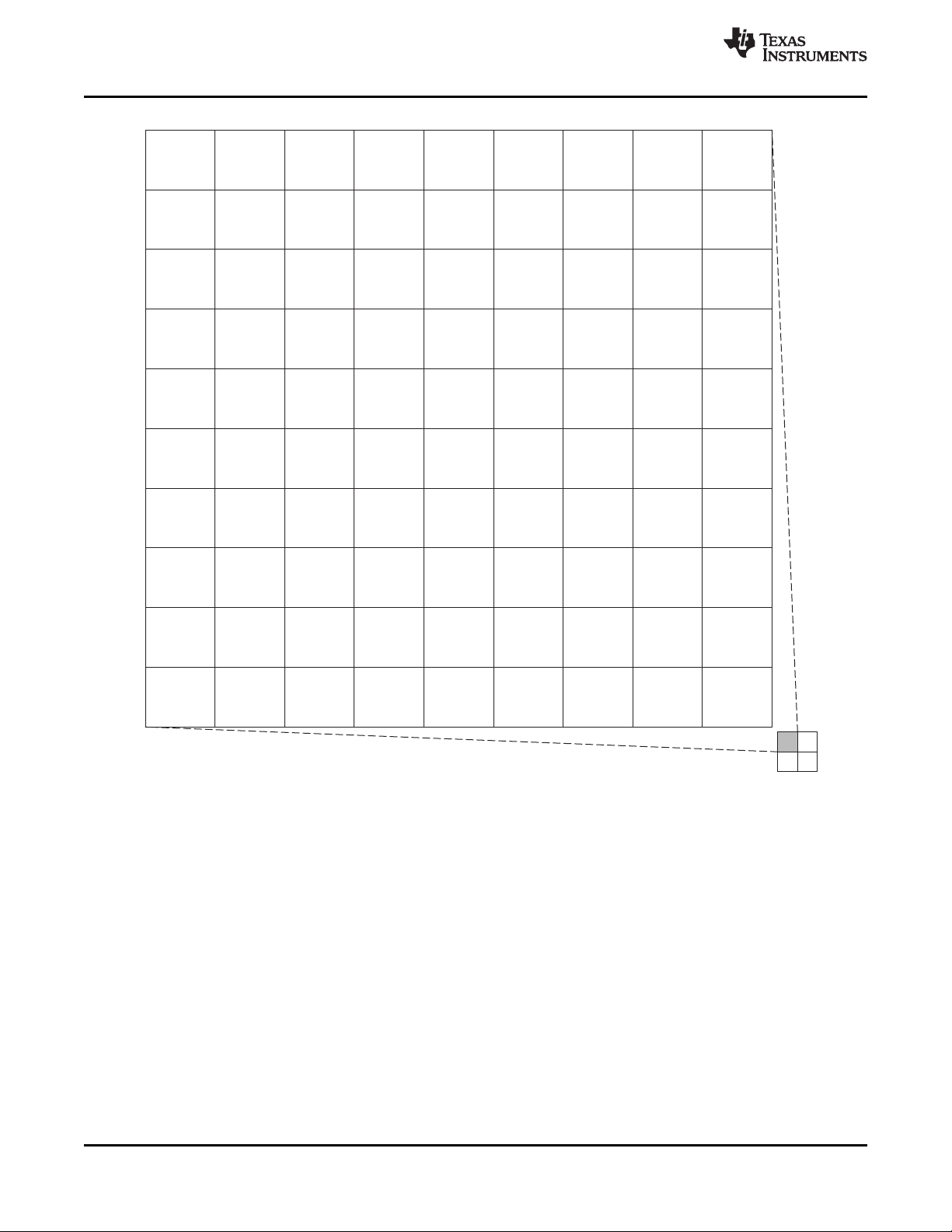
Lens Dist
Face Det
IPIPE
Resizer
ISIF
Video FE
3Ch
DAC
Video
Encoder
OSD
Video BE
Buffer
SDTV/HDTV
Analog Video
Digital
RGB/YUV
Camera
AFE
VPSS
DDR2
Controller
EDMA
NAND/SM
Memory
I/F
HPI
16-Bit
DDR2/
mDDR
NAND/
OneNAND/
NOR Flash,
SmartMedia/
xD
Host CPU
16 Bit
8/16 Bit
16 Bit
USB2.0 HS w/OTG
MMC/SD (x2)
SPI (x5)
UART (x2)
I2C
Timer (x4-64b)
WDT (x1-64b)
GIO
PWM (x4)
RTO
McBSP
EMAC
ADC
Key Scan
Voice Codec
System
I/O
Interface
I-Cache
16 KB
D-Cache
8 KB
RAM
32 KB
ROM
16 KB
ARM926EJ-S
ARM INTC
PRTCSS
CLOCK Ctrl
PLL
JTAG
I/F
HDVICP MJCP
DMA/Data and Configuration Bus
19.2 MHz, 24 MHz
27 MHz or 36 MHz
32.768
kHz
PMIC/
SW
TMS320DM368
SPRS668B–APRIL 2010–REVISED NOVEMBER 2010
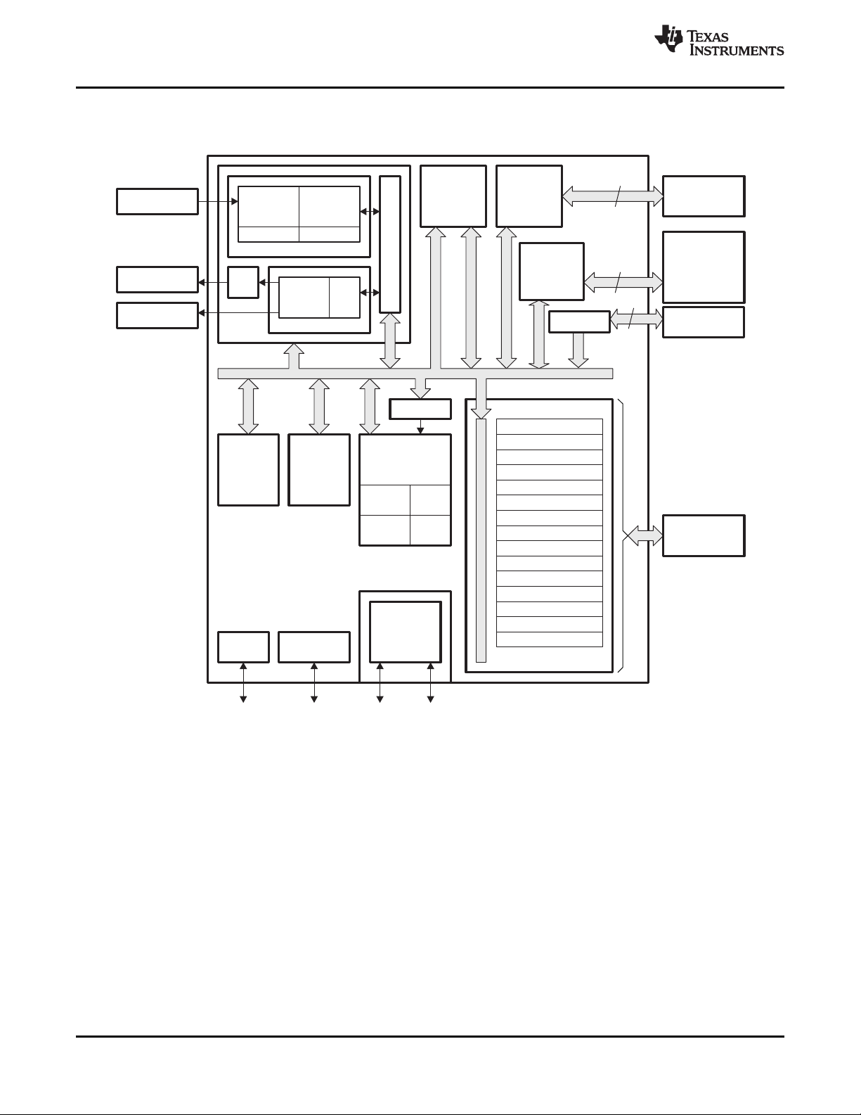
1.3 Functional Block Diagram
Figure 1-1 shows the functional block diagram of the TMS320DM368 device.
www.ti.com
4 TMS320DM368 Digital Media System-on-Chip (DMSoC) Copyright © 2010, Texas Instruments Incorporated
Figure 1-1. Functional Block Diagram
Submit Documentation Feedback
Product Folder Link(s): TMS320DM368
Page 5

TMS320DM368
www.ti.com
SPRS668B–APRIL 2010–REVISED NOVEMBER 2010
1 TMS320DM368 Digital Media System-on-Chip 6 Peripheral Information and Electrical
(DMSoC) ................................................... 1 Specifications .......................................... 76
1.1 Features .............................................. 1
1.2 Description ........................................... 3
1.3 Functional Block Diagram ............................ 4
Revision History (Revision B) ............................. 6
2 Device Overview ........................................ 7
2.1 Device Characteristics ............................... 7
2.2 Device Compatibility ................................. 8
2.3 ARM Subsystem Overview .......................... 8
2.4 System Control Module ............................. 12
2.5 Power Management ................................ 13
2.6 Memory Map Summary ............................. 14
2.7 Pin Assignments .................................... 16
2.8 Terminal Functions ................................. 21
2.9 Device Support ..................................... 46
3 Device Configurations ................................ 50
3.1 System Module Registers .......................... 50
3.2 Boot Modes ......................................... 51
3.3 Device Clocking .................................... 54
3.4 Power and Sleep Controller (PSC) ................. 61
3.5 Pin Multiplexing ..................................... 63
3.6 Device Reset ....................................... 64
3.7 Default Device Configurations ...................... 64
3.8 Debugging Considerations ......................... 69
4 System Interconnect .................................. 70
5 Device Operating Conditions ....................... 71
5.1 Absolute Maximum Ratings Over Operating Case
Temperature Range
(Unless Otherwise Noted) ................................. 71
5.2 Recommended Operating Conditions .............. 72
5.3 Electrical Characteristics Over Recommended
Ranges of Supply Voltage
and Operating Case Temperature (Unless
Otherwise Noted) ................................... 74
6.1 Parameter Information Device-Specific Information
...................................................... 76
6.2 Recommended Clock and Control Signal Transition
Behavior ............................................ 77
6.3 Power Supplies ..................................... 77
6.4 Power-Supply Sequencing ......................... 78
6.5 Reset ............................................... 80
6.6 Oscillators and Clocks .............................. 81
6.7 Power Management and Real Time Clock
Subsystem (PRTCSS) .............................. 85
6.8 General-Purpose Input/Output (GPIO) ............. 87
6.9 EDMA Controller .................................... 89
6.10 External Memory Interface (EMIF) ................. 99
6.11 MMC/SD ........................................... 120
6.12 Video Processing Subsystem (VPSS) Overview
..................................................... 123
6.13 USB 2.0 ........................................... 147
6.14 Universal Asynchronous Receiver/Transmitter
(UART) ............................................ 155
6.15 Serial Port Interface (SPI) ......................... 157
6.16 Inter-Integrated Circuit (I2C) ...................... 167
6.17 Multi-Channel Buffered Serial Port (McBSP) ..... 170
6.18 Timer .............................................. 179
6.19 Pulse Width Modulator (PWM) .................... 181
6.20 Real Time Out (RTO) ............................. 183
6.21 Ethernet Media Access Controller (EMAC) ....... 185
6.22 Management Data Input/Output (MDIO) .......... 191
6.23 Host-Port Interface (HPI) Peripheral .............. 193
6.24 Key Scan .......................................... 197
6.25 Analog-to-Digital Converter (ADC) ................ 199
6.26 Voice Codec ....................................... 199
6.27 IEEE 1149.1 JTAG ................................ 201
7 Mechanical Data ...................................... 204
7.1 Thermal Data for ZCE ............................. 204
7.2 Packaging Information ............................ 204
Copyright © 2010, Texas Instruments Incorporated Contents 5
Submit Documentation Feedback
Product Folder Link(s): TMS320DM368
Page 6

TMS320DM368
SPRS668B–APRIL 2010–REVISED NOVEMBER 2010
NOTE: Page numbers for previous revisions may differ from page numbers in the current version.
highlights the technical changes made to the SPRS668A device-specific data sheet to make it an
SPRS668B revision.
See Additions/Changes/Deletions
Table 6-23 Updated table note.
Table 6-96 Corrected hold time for t
Section 6.7 Added last 3 bullets.
Section 6.8 Changed second bullet.
www.ti.com
Revision History
Revision B Updates
h(MDCLKH-MDIO)
6 Contents Copyright © 2010, Texas Instruments Incorporated
Submit Documentation Feedback
Product Folder Link(s): TMS320DM368
Page 7
TMS320DM368
www.ti.com
SPRS668B–APRIL 2010–REVISED NOVEMBER 2010
2 Device Overview
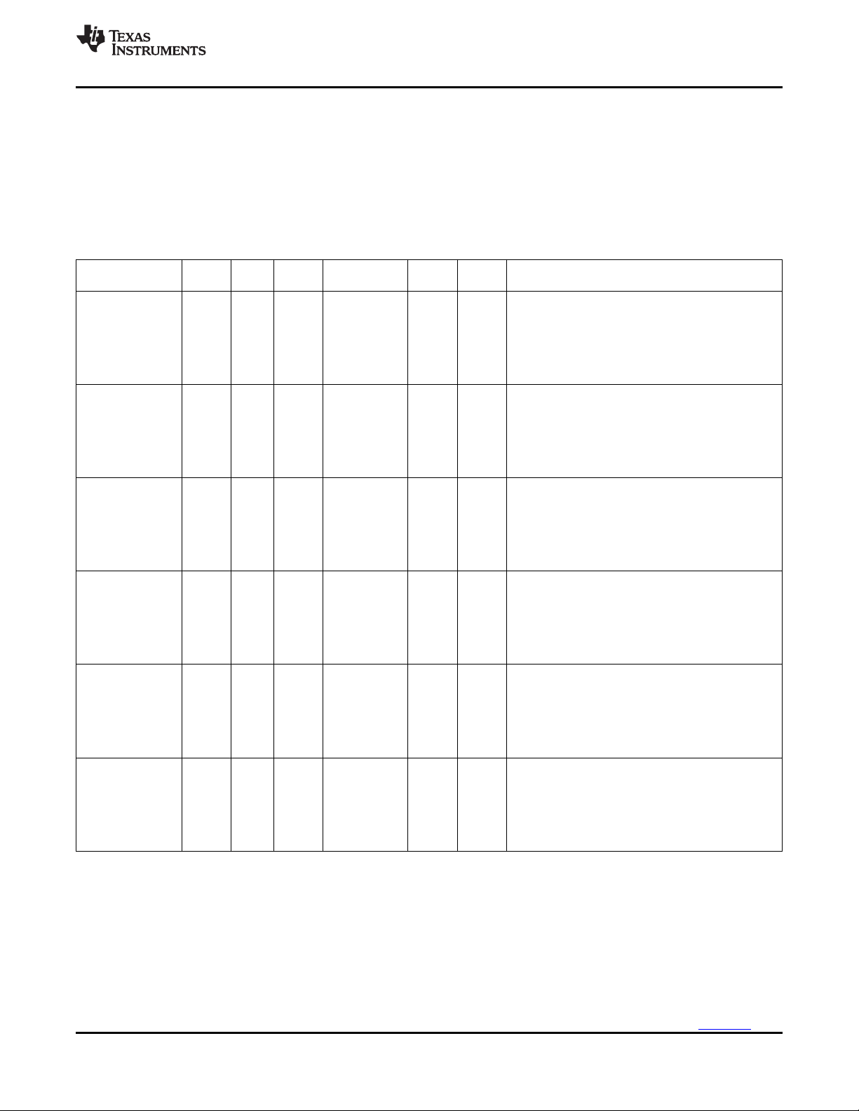
2.1 Device Characteristics
Table 2-1 provides an overview of the DMSoC. The table shows significant features of the device,
including the peripherals, capacity of on-chip RAM, ARM operating frequency, the package type with pin
count, etc.
Table 2-1. Characteristics of the Processor
HARDWARE FEATURES DEVICE
DDR2 / mDDR Memory Controller DDR2 / mDDR (16-bit bus width)
Asynchronous EMIF (AEMIF)
Flash Card Interfaces
EDMA
Timers configurable as two separate 32-bit timers)
UART Two (one with RTS and CTS flow control)
Peripherals
Not all peripherals pins are
available at the same time (For
more detail, see the Device
Configuration section).
On-Chip CPU Memory Organization 16-KB I-cache, 8-KB D-cache, 32-KB RAM,
JTAG BSDL_ID JTAGID register (address location: 0x01C4 0028)
CPU Frequency (Maximum) MHz ARM: 432-MHz
Voltage
PLL Options
BGA Package 13 x 13 mm 338-Pin BGA (ZCE)
Process Technology 65 nm
SPI Five (each supports two slave devices)
I2C One (Master/Slave)
10/100 Ethernet MAC with Management Data I/O One
Multi-Channel Buffered Serial Port [McBSP] One McBSP
Power Management and Real Time Clock Subsystem
(PRTCSS)
Key Scan 4 x 4 Matrix, 5 x 3 Matrix
Voice Codec One
Analog-to-Digital Converter (ADC) 6-channel, 10-bit Interface
General-Purpose Input/Output Port Up to 104
Pulse width modulator (PWM) Four outputs
Configurable Video Ports
USB 2.0 High Speed Host
Wireless Interfaces Through SDIO
RTO Four Channels
Core (V) 1.35 V
I/O (V) 3.3 V, 1.8 V
Reference frequency options 19.2 MHz, 24 MHz, 27 MHz, 36 MHz
Configurable PLL controller PLL bypass, programmable PLL
Asynchronous (8/16-bit bus width) RAM,
Flash (NOR, NAND, OneNAND)
Two MMC/SD
One SmartMedia/xD
64 independent DMA channels
Eight QDMA channels
Four 64-Bit General Purpose (each
One 64-Bit Watch Dog
RTC (32.768kHz), GPIO
One Input (VPFE)
One Output (VPBE)
High Speed Device
On The Go (HS-USB-OTG)
ARM
16-KB ROM
See Section 6.27.1, JTAG Register
Description(s)
Copyright © 2010, Texas Instruments Incorporated Device Overview 7
Submit Documentation Feedback
Product Folder Link(s): TMS320DM368
Page 8

TMS320DM368
SPRS668B–APRIL 2010–REVISED NOVEMBER 2010
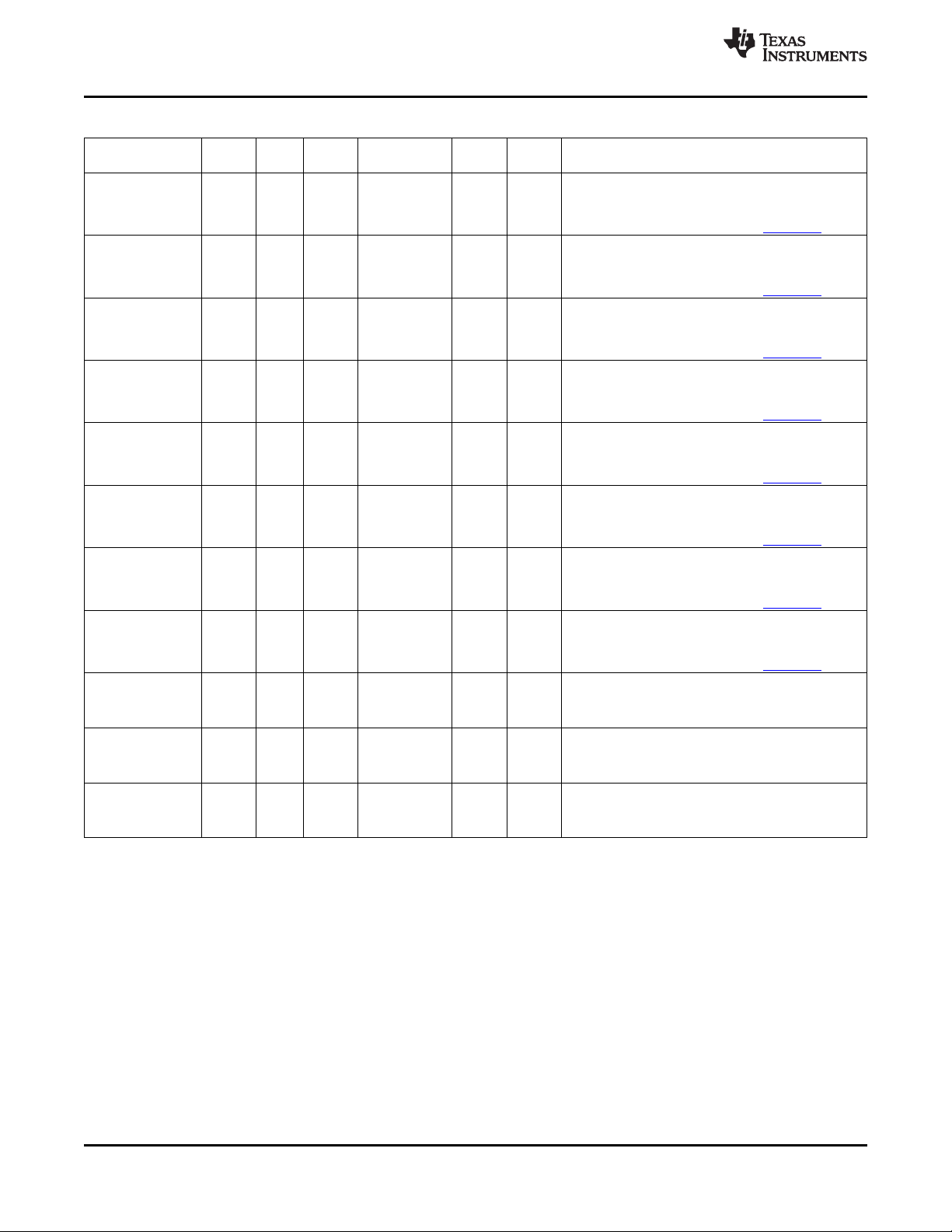
Table 2-1. Characteristics of the Processor (continued)
HARDWARE FEATURES DEVICE
Product Status
(1) PRODUCTION DATA information is current as of publication date. Products conform to specifications per the terms of Texas
Instruments standard warranty. Production processing does not necessarily include testing of all parameters.
(1)
Product Preview (PP),
Advance Information (AI), PD
or Production Data (PD)
2.2 Device Compatibility
The ARM926EJ-S RISC CPU is compatible with other ARM9 CPUs from ARM Holdings plc.
2.3 ARM Subsystem Overview
The ARM Subsystem contains components required to provide the ARM926EJ-S (ARM) master control of
the overall device system, including the components of the ARM Subsystem, the peripherals, and the
external memories.
The ARM is responsible for handling system functions such as system-level initialization, configuration,
user interface, user command execution, connectivity functions, interface and control of the subsystem,
etc. The ARM is master and performs these functions because it has a large program memory space and
fast context switching capability, and is thus suitable for complex, multi-tasking, and general-purpose
control tasks.
2.3.1 Components of the ARM Subsystem
www.ti.com
The ARM Subsystem consists of the following components:
• ARM926EJ-S RISC processor, including:
– coprocessor 15 (CP15)
– MMU
– 16KB Instruction cache
– 8KB Data cache
– Write Buffer
– Java accelerator
• ARM Internal Memories
– 32KB Internal RAM (32-bit wide access)
– 16KB Internal ROM (ARM bootloader for non-AEMIF boot modes)
• Embedded Trace Module and Embedded Trace Buffer (ETM/ETB)
• System Control Peripherals
– ARM Interrupt Controller
– PLL Controller
– Power and Sleep Controller
– System Control Module
The ARM also manages/controls all the device peripherals.
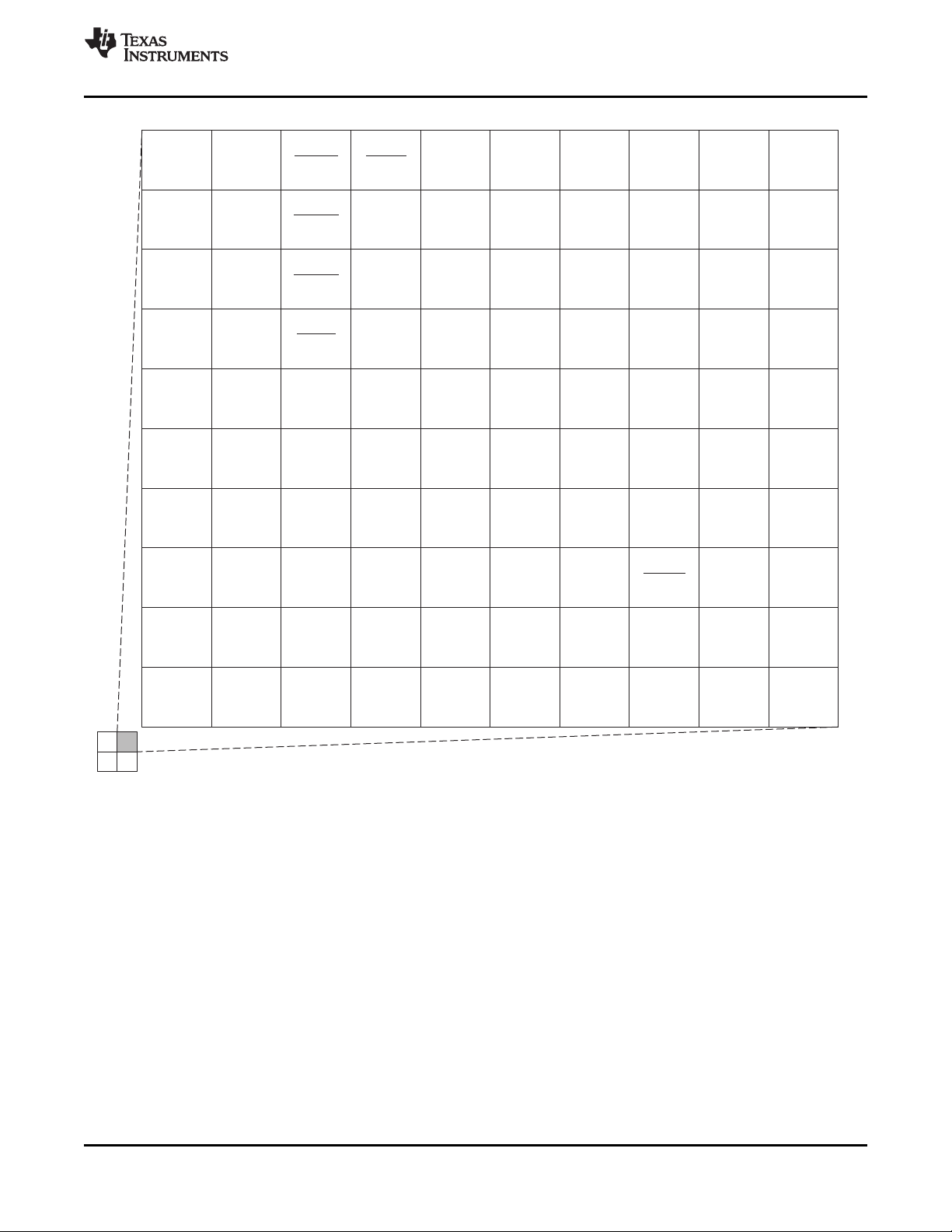
Figure 2-1 shows the functional block diagram of the ARM Subsystem.
8 Device Overview Copyright© 2010, Texas Instruments Incorporated
Submit Documentation Feedback
Product Folder Link(s): TMS320DM368
Page 9
ARM926EJ-S
16KI$
8KD$ MMU
CP15
Arbiter Arbiter
I-AHB
D-AHB
Master
IF
DMA Bus
I-TCM
D-TCM
16K
RAM0
RAM1
16K
ROM
16K
Arbiter
Slave
IF
MasterIF
CFGBus
ARM
Interrupt
Controller
(AINTC)
Control
System
PLLC2
PLLC1
(PSC)
Controller
Sleep
Power
Peripherals
...
TMS320DM368
www.ti.com
SPRS668B–APRIL 2010–REVISED NOVEMBER 2010
2.3.2 ARM926EJ-S RISC CPU
The ARM Subsystem integrates the ARM926EJ-S processor. The ARM926EJ-S processor is a member of
ARM9 family of general-purpose microprocessors. This processor is targeted at multi-tasking applications
where full memory management, high performance, low die size, and low power are all important. The
ARM926EJ-S processor supports the 32-bit ARM and 16 bit THUMB instruction sets, enabling the user to
trade off between high performance and high code density. Specifically, the ARM926EJ-S processor
supports the ARMv5TEJ instruction set, which includes features for efficient execution of Java byte codes,
providing Java performance similar to Just in Time (JIT) Java interpreter, but without associated code
overhead.
The ARM926EJ-S processor supports the ARM debug architecture and includes logic to assist in both
hardware and software debug. The ARM926EJ-S processor has a Harvard architecture and provides a
complete high performance subsystem, including:
• ARM926EJ -S integer core
• CP15 system control coprocessor
• Memory Management Unit (MMU)
• Separate instruction and data Caches
• Write buffer
• Separate instruction and data Tightly-Coupled Memories (TCMs) [internal RAM] interfaces
• Separate instruction and data AHB bus interfaces
• Embedded Trace Module and Embedded Trace Buffer (ETM/ETB)
For more complete details on the ARM9, refer to the ARM926EJ-S Technical Reference Manual, available
at http://www.arm.com
Figure 2-1. ARM Subsystem Block Diagram
Copyright © 2010, Texas Instruments Incorporated Device Overview 9
Submit Documentation Feedback
Product Folder Link(s): TMS320DM368
Page 10

TMS320DM368
SPRS668B–APRIL 2010–REVISED NOVEMBER 2010
2.3.3 CP15
The ARM926EJ-S system control coprocessor (CP15) is used to configure and control instruction and
data caches, Tightly-Coupled Memories (TCMs), Memory Management Unit (MMU), and other ARM
subsystem functions. The CP15 registers are programmed using the MRC and MCR ARM instructions,
when the ARM in a privileged mode such as supervisor or system mode.
2.3.4 MMU
The ARM926EJ-S MMU provides virtual memory features required by operating systems such as Linux,
WindowCE, ultron, ThreadX, etc. A single set of two level page tables stored in main memory is used to
control the address translation, permission checks and memory region attributes for both data and
instruction accesses. The MMU uses a single unified Translation Lookaside Buffer (TLB) to cache the
information held in the page tables. The MMU features are:
• Standard ARM architecture v4 and v5 MMU mapping sizes, domains and access protection scheme.
• Mapping sizes are:
– 1MB (sections)
– 64KB (large pages)
– 4KB (small pages)
– 1KB (tiny pages)
• Access permissions for large pages and small pages can be specified separately for each quarter of
the page (subpage permissions)
• Hardware page table walks
• Invalidate entire TLB, using CP15 register 8
• Invalidate TLB entry, selected by MVA, using CP15 register 8
• Lockdown of TLB entries, using CP15 register 10
www.ti.com
2.3.5 Caches and Write Buffer
The size of the Instruction Cache is 16KB, Data cache is 8KB. Additionally, the Caches have the following
features:
• Virtual index, virtual tag, and addressed using the Modified Virtual Address (MVA)
• Four-way set associative, with a cache line length of eight words per line (32-bytes per line) and with
two dirty bits in the Dcache
• Dcache supports write-through and write-back (or copy back) cache operation, selected by memory
region using the C and B bits in the MMU translation tables.
• Critical-word first cache refilling
• Cache lockdown registers enable control over which cache ways are used for allocation on a line fill,
providing a mechanism for both lockdown, and controlling cache corruption
• Dcache stores the Physical Address TAG (PA TAG) corresponding to each Dcache entry in the TAG
RAM for use during the cache line write-backs, in addition to the Virtual Address TAG stored in the
TAG RAM. This means that the MMU is not involved in Dcache write-back operations, removing the
possibility of TLB misses related to the write-back address.
• Cache maintenance operations provide efficient invalidation of, the entire Dcache or Icache, regions of
the Dcache or Icache, and regions of virtual memory.
The write buffer is used for all writes to a noncachable bufferable region, write-through region and write
misses to a write-back region. A separate buffer is incorporated in the Dcache for holding write-back for
cache line evictions or cleaning of dirty cache lines. The main write buffer has 16-word data buffer and a
four-address buffer. The Dcache write-back has eight data word entries and a single address entry.
2.3.6 Tightly Coupled Memory (TCM)
ARM internal RAM is provided for storing real-time and performance-critical code/data and the Interrupt
10 Device Overview Copyright © 2010, Texas Instruments Incorporated
Submit Documentation Feedback
Product Folder Link(s): TMS320DM368
Page 11

TMS320DM368
www.ti.com
SPRS668B–APRIL 2010–REVISED NOVEMBER 2010
Vector table. ARM internal ROM boot modes include NAND, MMC/SD, UART, USB, SPI, EMAC, and HPI.
The RAM and ROM memories interfaced to the ARM926EJ-S via the tightly coupled memory interface
that provides for separate instruction and data bus connections. Since the ARM TCM does not allow
instructions on the D-TCM bus or data on the I-TCM bus, an arbiter is included so that both data and
instructions can be stored in the internal RAM/ROM. The arbiter also allows accesses to the RAM/ROM
from extra-ARM sources (e.g., EDMA or other masters). The ARM926EJ-S has built-in DMA support for
direct accesses to the ARM internal memory from a non-ARM master. Because of the time-critical nature
of the TCM link to the ARM internal memory, all accesses from non-ARM devices are treated as DMA
transfers.
Instruction and Data accesses are differentiated via accessing different memory map regions, with the
instruction region from 0x0000 through 0x7FFF and data from 0x10000 through 0x17FFF. Placing the
instruction region at 0x0000 is necessary to allow the ARM Interrupt Vector table to be placed at 0x0000,
as required by the ARM architecture. The internal 32-KB RAM is split into two physical banks of 16KB
each, which allows simultaneous instruction and data accesses to be accomplished if the code and data
are in separate banks.
2.3.7 Advanced High-performance Bus (AHB)
The ARM Subsystem uses the AHB port of the ARM926EJ-S to connect the ARM to the configuration bus
and the external memories. Arbiters are employed to arbitrate access to the separate D-AHB and I-AHB
by the configuration bus and the external memories bus.
2.3.8 Embedded Trace Macrocell (ETM) and Embedded Trace Buffer (ETB)
To support real-time trace, the ARM926EJ-S processor provides an interface to enable connection of an
Embedded Trace Macrocell (ETM). The ARM926ES-J Subsystem also includes the Embedded Trace
Buffer (ETB). The ETM consists of two parts:
• Trace Port provides real-time trace capability for the ARM9.
• Triggering facilities provide trigger resources, which include address and data comparators, counter,
and sequencers.
The device trace port is not pinned out and is instead only connected to the Embedded Trace Buffer. The
ETB has a 4KB buffer memory. ETB enabled debug tools are required to read/interpret the captured trace
data.
2.3.9 ARM Memory Mapping
The ARM memory map is shown in Table 2-3 and Table 2-4. This section describes the memories and
interfaces within the ARM's memory map.
2.3.9.1 ARM Internal Memories
The ARM has access to the following ARM internal memories:
• 32KB ARM Internal RAM on TCM interface, logically separated into two 16KB pages to allow
simultaneous access on any given cycle if there are separate accesses for code (I-TCM bus) and data
(D-TCM) to the different memory regions.
• 16KB ARM Internal ROM
2.3.9.2 External Memories
The ARM has access to the following External memories:
• DDR2 / mDDR Synchronous DRAM
• Asynchronous EMIF / OneNAND / NOR
• NAND Flash
• Flash card devices:
– MMC/SD
Copyright © 2010, Texas Instruments Incorporated Device Overview 11
Submit Documentation Feedback
Product Folder Link(s): TMS320DM368
Page 12

TMS320DM368
SPRS668B–APRIL 2010–REVISED NOVEMBER 2010
– xD
– SmartMedia
2.3.10 Peripherals
The ARM has access to all of the peripherals on the device.
2.3.11 ARM Interrupt Controller (AINTC)
The device ARM Interrupt Controller (AINTC) has the following features:
• Supports up to 64 interrupt channels (16 external channels)
• Interrupt mask for each channel
• Each interrupt channel can be mapped to a Fast Interrupt Request (FIQ) or to an Interrupt Request
(IRQ) type of interrupt.
• Hardware prioritization of simultaneous interrupts
• Configurable interrupt priority (2 levels of FIQ and 6 levels of IRQ)
• Configurable interrupt entry table (FIQ and IRQ priority table entry) to reduce interrupt processing time
The ARM core supports two interrupt types: FIQ and IRQ. See the ARM926EJ-S Technical Reference
Manual for detailed information about the ARM’s FIQ and IRQ interrupts. Each interrupt channel is
mappable to an FIQ or to an IRQ type of interrupt, and each channel can be enabled or disabled. The
INTC supports user-configurable interrupt-priority and interrupt entry addresses. Entry addresses minimize
the time spent jumping to interrupt service routines (ISRs). When an interrupt occurs, the corresponding
highest priority ISR’s address is stored in the INTC’s ENTRY register. The IRQ or FIQ interrupt routine can
read the ENTRY register and jump to the corresponding ISR directly. Thus, the ARM does not require a
software dispatcher to determine the asserted interrupt.
www.ti.com
2.4 System Control Module
The system control module is a system-level module containing status and top-level control logic required
by the device. The system control module consists of a miscellaneous set of status and control registers,
accessible by the ARM and supporting all of the following system features and operations:
• Device identification
• Device configuration
– Pin multiplexing control
– Device boot configuration status
• ARM interrupt and EDMA event multiplexing control
• Special peripheral status and control
– Timer64
– USB PHY control
– VPSS clock and video DAC control and status
– DDR VTP control
– Clockout circuitry
– GIO de-bounce control
• Power management
– Deep sleep
• Bandwidth Management
– Bus master DMA priority control
For more information on the System Control Module refer to Section 3, Device Configurations and the
TMS320DM36x DMSoC ARM Subsystem Reference Guide (literature number SPRUFG5).
12 Device Overview Copyright © 2010, Texas Instruments Incorporated
Submit Documentation Feedback
Product Folder Link(s): TMS320DM368
Page 13

TMS320DM368
www.ti.com
SPRS668B–APRIL 2010–REVISED NOVEMBER 2010
2.5 Power Management
The device is designed for minimal power consumption. There are two components to power
consumption: active power and leakage power. Active power is the power consumed to perform work and
scales with clock frequency and the amount of computations being performed. Active power can be
reduced by controlling the clocks in such a way as to either operate at a clock setting just high enough to
complete the required operation in the required time-line or to run at a clock setting until the work is
complete and then drastically cut the clocks (e.g. to PLL Bypass mode) until additional work must be
performed. Leakage power is due to static current leakage and occurs regardless of the clock rate.
Leakage, or standby power, is unavoidable while power is applied and scales roughly with the operating
junction temperatures. Leakage power can only be avoided by removing power completely from a device
or subsystem. The device includes several power management modes which are briefly described in
Table 2-2. See the TMS320DM36x DMSoC ARM Subsystem Reference Guide (literature number
SPRUFG5) for more information on power management.
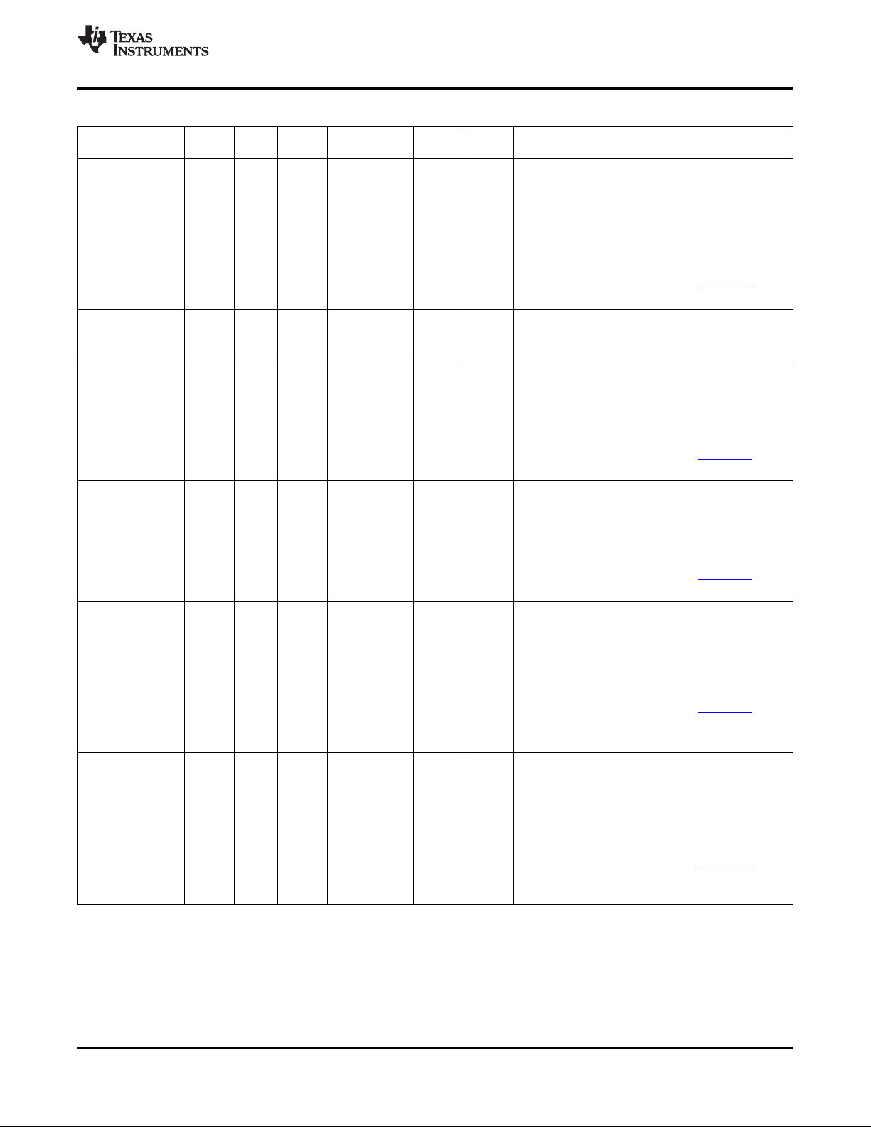
Table 2-2. Power Management Conditions
POWER MGMT. OTHER DDR
APPLICATION PRTCSS PERIPH. CLOCK/ DESCRIPTION
SCENARIO CLOCKS MODE
PRTCSS Active Off Off Off Off Off Off Off Off
Deep Sleep Mode
Standby Active On On Off On Off Off "Self- device. Clocks are
Low-power Bypass timers. Since ARM will
(PLL Bypass Mode) Mode not have access to
System Running
(PLL Mode)
(1)
Active On Off Off Off Off Off "Self- for PRTCSS and core
Active On On On On / Off On / Off On / Off "Self-
Active On On PLL Mode On On / Off On / Off On / Off Clock / This condition
CORE OSC. PLL ARM926 UART, PWM,
POWER POWER CNTRLR. CLOCK I2C TIMER
Bypass
Mode
(not
Active)
Bypass
Mode
(1) For more details, see TMS320DM36x DMSoC ARM Subsystem Reference Guide (literature number SPRUFG5)
GIO, SPI,
CLOCKS CLOCKS
This condition
consumes the lowest
possible power, except
for the PRTCSS.
This mode consumes
Suspend / possible power, except
Refresh" power, where only the
Suspend / in order to wake up the
Refresh" suspended except for
Suspend /
Refresh"
Nominal system PLLs, are on.
Operation conserves the least
the second lowest
deep sleep circuit is on
in this mode.
This condition keeps
the minimum possible
modules powered-on
GIO (interrupts),
UART, and I2C (in
slave mode).
Most clocks are
suspended, except for
ARM, GIO, UART,
SPI, I2C, PWM, and
DDR, its internal
Cache will be either
frozen or not
accessed.
The device, including
amount of power.
Copyright © 2010, Texas Instruments Incorporated Device Overview 13
Submit Documentation Feedback
Product Folder Link(s): TMS320DM368
Page 14
TMS320DM368
SPRS668B–APRIL 2010–REVISED NOVEMBER 2010
www.ti.com
2.6 Memory Map Summary
Table 2-3 shows the memory map address ranges of the device. Table 2-4 depicts the expanded map of
the Configuration Space (0x01C0 0000 through 0x01FF FFFF). The device has multiple on-chip memories
associated with its processor and various subsystems. To help simplify software development a unified
memory map is used where possible to maintain a consistent view of device resources across all bus
masters. The bus masters are the ARM, EDMA, EMAC, USB, HPI, MJCP, HDVICP and VPSS. The
Master Peripherals are EMAC, USB, and HPI. Please refer to Section 4 for more details.
Table 2-3. Memory Map
Start Address End Address Size (Bytes) ARM EDMA Master Periph VPSS
0x0000 0000 0x0000 3FFF 16K ARM RAM0
0x0000 4000 0x0000 7FFF 16K ARM RAM1
0x0000 8000 0x0000 BFFF 16K ARM ROM
0x0000 C000 0x0000 FFFF 16K Reserved
0x0001 0000 0x0001 3FFF 16K ARM RAM0 (Data) ARM RAM0 ARM RAM0
0x0001 4000 0x0001 7FFF 16K ARM RAM1 (Data) ARM RAM1 ARM RAM1
0x0001 8000 0x0001 BFFF 16K ARM ROM ARM ROM ARM ROM
0x0001 C000 0x000F FFFF 912K Reserved
0x0010 0000 0x01BB FFFF 26M
0x01BC 0000 0x01BC 0FFF 4K ARM ETB Mem
0x01BC 1000 0x01BC 17FF 2K ARM ETB Reg Reserved
0x01BC 1800 0x01BC 18FF 256 ARM IceCrusher Reserved
0x01BC 1900 0x01BC FFFF 59136 Reserved
0x01BD 0000 0x01BF FFFF 192K
0x01C0 0000 0x01FF FFFF 4M CFG Bus CFG Bus CFG Bus
0x0200 0000 0x09FF FFFF 128M ASYNC EMIF (Data) ASYNC EMIF (Data)
0x0A00 0000 0x11EF FFFF 127M - 16K Reserved Reserved
0x11F0 0000 0x11F1 FFFF 128K MJCP DMA Port MJCP DMA Port
0x11F2 0000 0x11FF FFFF 896K Reserved Reserved
0x1200 0000 0x1207 FFFF 512K HDVICP DMA Port1 HDVICP DMA Port1 HDVICP
0x1208 0000 0x120F FFFF 512K Reserved HDVICP DMA Port2 Reserved
0x1210 0000 0x1217 FFFF 512K HDVICP DMA Port3
0x1218 0000 0x1FFF FFFF 222.5M Reserved
0x2000 0000 0x2000 7FFF 32K DDR EMIF Control DDR EMIF Control
0x2000 8000 0x41FF FFFF 544M-32K
0x4200 0000 0x49FF FFFF 128M Reserved Reserved
0x4A00 0000 0x7FFF FFFF 864M
0x8000 0000 0x8FFF FFFF 256M DDR EMIF DDR EMIF DDR EMIF DDR EMIF
0x9000 0000 0xFFFF FFFF 1792M Reserved Reserved Reserved Reserved
Mem Map Mem Map Mem Map Mem Map
(Instruction)
(Instruction)
(Instruction)
Peripherals Peripherals Peripherals
Regs Regs
Reserved Reserved
DMA Port1
14 Device Overview Copyright © 2010, Texas Instruments Incorporated
Submit Documentation Feedback
Product Folder Link(s): TMS320DM368
Page 15
TMS320DM368
www.ti.com
SPRS668B–APRIL 2010–REVISED NOVEMBER 2010
Table 2-4. ARM Configuration Bus Access to Peripherals
Address
Region Start End Size
EDMA CC 0x01C0 0000 0x01C0 FFFF 64K
EDMA TC0 0x01C1 0000 0x01C1 03FF 1K
EDMA TC1 0x01C1 0400 0x01C1 07FF 1K
EDMA TC2 0x01C1 0800 0x01C1 0BFF 1K
EDMA TC3 0x01C1 0C00 0x01C1 0FFF 1K
Reserved 0x01C1 1000 0x01C1 FFFF 60 K
UART0 0x01C2 0000 0x01C2 03FF 1K
Reserved 0x01C2 0400 0x01 20 7FFF 1K
Timer 3 0x01C2 0800 0x01C2 0BFF 1K
Real-time out 0x01C2 0C00 0x01C2 0FFF 1K
I2C 0x01C2 1000 0x01C2 13FF 1K
Timer 0 0x01C2 1400 0x01C2 17FF 1K
Timer 1 0x01C2 1800 0x01C2 1BFF 1K
Timer 2 0x01C2 1C00 0x01C2 1FFF 1K
PWM0 0x01C2 2000 0x01C2 23FF 1K
PWM1 0x01C2 2400 0x01C2 27FF 1K
PWM2 0x01C2 2800 0x01C2 2BFF 1K
PWM3 0x01C2 2C00 0x01C2 2FFF 1K
SPI4 0x01C2 3000 0x01C2 37FF 2K
Timer 4 0x01C2 3800 0x01C2 3BFF 1K
ADCIF 0x01C2 3C00 0x01C2 3FFF 1K
Reserved 0x01C2 4000 0x01C3 4FFF 112K
System Module 0x01C4 0000 0x01C4 07FF 2K
PLL Controller 1 0x01C4 0800 0x01C4 0BFF 1K
PLL Controller 2 0x01C4 0C00 0x01C4 0FFF 1K
Power/Sleep Controller 0x01C4 1000 0x01C4 1FFF 4K
Reserved 0x01C4 2000 0x01C4 7FFF 24K
ARM Interrupt Controller 0x01C4 8000 0x01C4 83FF 1K
Reserved 0x01 C4 8400 0x01C63FFF 111K
USB OTG 2.0 Regs / RAM 0x01C6 4000 0x01C6 5FFF 8K
SPI0 0x01C6 6000 0x01C6 67FF 2K
SPI1 0x01C6 6800 0x01C6 6FFF 2K
GPIO 0x01C6 7000 0x01C6 77FF 2K
SPI2 0x01C6 7800 0x01C6 FFFF 2K
SPI3 0x01C6 8000 0x01C6 87FF 2K
Reserved 0x01C6 8800 0x01C6 87FF 2K
PRTCSS Interface Registers 0x01C6 9000 0x01C6 93FF 1K
KEYSCAN 0x01C6 9400 0x01C6 97FF 1K
HPI 0x01C6 9800 0x01C6 9FFF 2K
Reserved 0x01C6 A000 0x01C6 FFFF 24K
VPSS Subsystem
ISP System Configuration Registers 0x01C7 0000 0x01C7 00FF 256
VPBE Clock Control Register 0x01C7 0200 0x01C7 02FF 256
Resizer Registers 0x01C7 0400 0x01C7 07FF 1K
IPIPE Registers 0x01C7 0800 0x01C7 0FFF 2K
ISIF Registers 0x01C7 1000 0x01C7 11FF 512
Copyright © 2010, Texas Instruments Incorporated Device Overview 15
Submit Documentation Feedback
Product Folder Link(s): TMS320DM368
Page 16
TMS320DM368
SPRS668B–APRIL 2010–REVISED NOVEMBER 2010
Table 2-4. ARM Configuration Bus Access to Peripherals (continued)
Address
IPIPEIF Registers 0x01C7 1200 0x01C7 12FF 768
Reserved 0x01C7 1400 0x01C7 17FF 768
FDIF Registers 0x01C7 1800 0x01C7 1BFF 1K
OSD Registers 0x01C7 1C00 0x01C7 1CFF 256
Reserved 0x01C7 1D00 0x01C7 1DFF 256
VENC Registers 0x01C7 1E00 0x01C7 1FFF 512
Reserved 0x01C7 2000 0x01CF FFFF 568K
Multimedia / SD 1 0x01D0 0000 0x01D0 1FFF 8K
McBSP 0x01D0 2000 0x01D0 3FFF 8K
Reserved 0x01D0 4000 0x01D0 5FFF 8K
UART1 0x01D0 6000 0x01D0 63FF 1K
Reserved 0x01D0 6400 0x01D0 7FFF 3K
EMAC Control Registers 0x01D0 7000 0x01D0 9FFF 0x01D0 7FFF4K
EMAC Control Module RAM 0x01D0 8000 8K
EMAC Control Module Registers 0x01D0 A000 0x01D0 AFFF 4K
EMAC MDIO Control Registers 0x01D0 B000 0x01D0 B7FF 2K
Voice Codec 0x01D0 C000 0x01D0 C3FF 1K
Reserved 0x01D0 C400 0x01D0 FFFF 17K
ASYNC EMIF Control 0x01D1 0000 0x01D1 0FFF 4K
Multimedia / SD 0 0x01D1 1000 0x01D1 FFFF 60K
Reserved 0x01D2 0000 0x01D3 FFFF 128K
Reserved 0x01D4 0000 0x01DF FFFF 768K
Reserved 0x01E0 0000 0x01FF FFFF 2M
ASYNC EMIF Data (CE0) 0x0200 0000 0x03FF FFFF 32M
ASYNC EMIF Data (CE1) 0x0400 0000 0x05FF FFFF 32M
Reserved 0x0600 0000 0x09FF FFFF 64M
Reserved 0x0A00 0000 0x0FFF FFFF 96M
www.ti.com
2.7 Pin Assignments
Extensive use of pin multiplexing is used to accommodate the largest number of peripheral functions in
the smallest possible package. Pin multiplexing is controlled using a combination of hardware
configuration at device reset and software programmable register settings.
2.7.1 Pin Map (Bottom View)
Figure 2-2 through Figure 2-5 show the pin assignments in four quadrants (A, B, C, and D). Note that
micro-vias are not required.
16 Device Overview Copyright © 2010, Texas Instruments Incorporated
Submit Documentation Feedback
Product Folder Link(s): TMS320DM368
Page 17

9
J
8
7
6
5
4
31
H
G
V
DD12_
PRTCSS
F
E
D
PWCTRO3
C
B
A
V
DDS18
PWCTRIO4PECTRIO0
V
SS
V
DDS33
EMU1RESET
RTCXO
V
DDA18_ADC
CV
DD
EMU0N.B.RTCXI
V
SSA_ADC
V
DDS33
TDITCKGIO21GIO20
V
DDA18_VC
ADC_CH0GIO44
GPIO46
V
DD18_SLDO
GIO17GIO19GIO16
V
SSA33_VC
ADC_CH3
GIO1
GIO49GIO13
GIO14
LINEO
MICIN
N.B.
GIO47
GIO3
GIO2
N.B.GIO12
SPP
MICIP
ADC_CH1
GPIO45
GIO0
GIO5GIO6GIO11
SPN
VCOM
ADC_CH2ADC_CH5
GIO48
GIO4GIO7
RSV0
2
PWCTRIO1
V
SS_32K
TMS
RTCK
GIO18
GIO15
GIO9
GIO10
GIO8
PWCTRIO2
CV
DD
V
SSA18_VC
ADC_CH4
V
DDRAM
V
DDS33
TDO N.B.
CV
DD
CV
DD
TRST
CV
DD
V
SS
TMS320DM368
www.ti.com
SPRS668B–APRIL 2010–REVISED NOVEMBER 2010
(1) N.B stands for No-Ball.
Figure 2-2. ZCE Pin Map [Quadrant A]
Copyright © 2010, Texas Instruments Incorporated Device Overview 17
Submit Documentation Feedback
Product Folder Link(s): TMS320DM368
Page 18
W
9
DDR_
DQ6
8
DDR_
DQ8
765
4
GIO36
32
GIO32
1
V
GIO38GIO34GIO23
U
DDR_
DQSN0
T
GIO24
R
P
N
M
L
K
DDR_
DQ12
DDR_
DQM1
GIO41
V
SS
DDR_
DQ5
DDR_
DQ11
DDR_
DQ14
DDR_
DQ15
GIO33
GIO28
DDR_DQ9N.B.
DDR_
DQSN1
GIO40
GIO35
GIO31N.B.GIO29GIO26
DDR_
DQGATE1
DDR_
DQGATE0
GIO43
GIO37GIO27
GIO25
DDR_DQ7DDR_DQ10DDR_DQ13GIO42
GIO39
RSV2V
PP
GIO22
RSV1
V
DD18_DDR
V
SS
V
DDS33
V
DDA33_USB
V
SSA33_USB
V
SSA18_USB
USB_DM
V
DD18_DDR
V
SS
V
DDS33
V
DD18_USB
N.B.
USB_VBUS
USB_DP
V
SS
V
SS
VDDA12LDO_
USB
V
SSA
PWRST
PWRCNTON
USB_ID
V
SS
V
DDMXI
PWCTRO1PWCTRO2PWCTRO3
V
SS_MX1
MXI1
V
SS
CV
DD
V
DD18_PRTCSS
PWCTRIO5
N.B.
PWCTRO0MXO1
V
DDS18
PWCTRIO6
V
DD12_PRTCSS
V
SS
V
SS
V
SS
N.B.
V
DDA18_PLL
V
DDS33
GIO30
DDR_DQS1
CV
DD
TMS320DM368
SPRS668B–APRIL 2010–REVISED NOVEMBER 2010
www.ti.com
(1) N.B stands for No-Ball.
Figure 2-3. ZCE Pin Map [Quadrant B]
18 Device Overview Copyright © 2010, Texas Instruments Incorporated
Submit Documentation Feedback
Product Folder Link(s): TMS320DM368
Page 19
V
SS
19
W
18
DDR_A11
17
DDR_A8
16
DDR_A6
15
DDR_A2
14
DDR_BA0
13
DDR_WE
12
DDR_CLK
11
DDR_CLK
10
DDR_DQ4
EM_A11
V
EM_A13
DDR_A12
DDR_A10DDR_A5
DDR_A1DDR_BA2
DDR_CASDDR_DQ1
DDR_DQ3
EM_A10
U
EM_A12
N.B.
DDR_A9DDR_A4
DDR_A0
N.B.DDR_RASDDR_DQ0
N.B.
EM_A8
T
EM_A9
EM_A7
DDR_A7
DDR_A3
DDR_CS
DDR_DQM0
EM_A4
R
EM_A6
EM_BA1
EM_A5
EM_A3
V
DD_
AEMIF1_18_33
DDR_CKE
V
DD18_DDR
DDR_
PADREFP
DDR_DQ2
EM_D13
P
EM_D15
EM_BA0EM_D14EM_D12
V
DD18_DDR
EM_D9
N
EM_D10N.B.EM_D8
V
SS
V
DD18_DDR
EM_A1
M
EM_A2
EM_CE[0]
EM_ADVEM_CLK
V
DDS18
EM_D5
L
EM_D6EM_A0EM_D7EM_D4
V
SS
EM_D2
K
EM_D0N.B.
DDR_VREF V
DD18_DDR
V
DD_
AEMIF1_18_33
V
DDS33
CV
DD
V
SS
CV
DD
V
DD_
AEMIF2_18_33
EM_D3
EM_D1
N.B.
V
SS
V
SS
CV
DD
CV
DD
V
SS
CV
DD
EM_D11
N.B.
V
SS
N.B.
V
SS
DDR_A13
DDR_BA1
DDR_DQS0
V
DD_
AEMIF2_18_33
TMS320DM368
www.ti.com
SPRS668B–APRIL 2010–REVISED NOVEMBER 2010
(1) N.B stands for No-Ball.
Figure 2-4. ZCE Pin Map [Quadrant C]
Copyright © 2010, Texas Instruments Incorporated Device Overview 19
Submit Documentation Feedback
Product Folder Link(s): TMS320DM368
Page 20

19181716151413121110
EM_OE
J
MMCSD0_
DATA1
H
YOUT6
G
F
E
D
C
V
DDS18
B
A
EM_WAITEM_CE[1]
MMCSD0_CLK
EM_WE
V
SS
MMCSD0_
DATA0
MMCSD0_
DATA3
MMCSD0_
CMD
VSYNC
N.B.
HSYNC
YOUT2
YOUT4YOUT1YOUT3
YOUT5
COUT6
COUT7COUT4
C_WE_
FIELD
VDDA12_DAC
VSSA18_
DAC
VDDA33_VC
COUT2COUT1COUT0
YIN0
YIN1
YIN4VREF
LCD_OEFIELD
N.B.CIN2
CIN6
HDN.B.YIN7
COMPPR
N.B.
VCLK
CIN1
CIN5
CIN4
CIN0
CIN3
YIN2
CIN7
VD
YIN3
YIN5
YIN6
COMPY
COMPPB
IDACOUT
IREF
V
DDS18
CV
DD
V
DDS33
V
DDS18
MMCSD0_
DATA2
V
SS
V
DD_ISIF18_33
V
DD_ISIF18_33
V
SSA12_DAC
V
DDS33
COUT5
EXTCLK
VFB
V
SS
TVOUT
V
DDA18_DAC
PCLK
COUT3
YOUT0V
SS
YOUT7N.B.
V
SS
V
SS
N.B.
V
SS
CV
DD
CV
DD
V
SS
V
SS
TMS320DM368
SPRS668B–APRIL 2010–REVISED NOVEMBER 2010
www.ti.com
(1) N.B stands for No-Ball.
Figure 2-5. ZCE Pin Map [Quadrant D]
20 Device Overview Copyright © 2010, Texas Instruments Incorporated
Submit Documentation Feedback
Product Folder Link(s): TMS320DM368
Page 21
TMS320DM368
www.ti.com
SPRS668B–APRIL 2010–REVISED NOVEMBER 2010
2.8 Terminal Functions
Table 2-5 provides a complete pin description list which shows external signal names, the associated pin
(ball) numbers along with the mechanical package designator, the pin type, whether the pin has any
internal pullup or pulldown resistors, and a functional pin description. For more detailed information on
device configuration, peripheral selection, multiplexed/shared pins, and debugging considerations, see
Section 3.
Table 2-5. Pin Descriptions
Name BGA Type Group Power IPU Reset Description
ID
(5)
CIN7
CIN6
CIN5
CIN4
CIN3
CIN2
(5)
(5)
(5)
(5)
(5)
A15 I/O ISIF V
C15 I/O ISIF V
B16 I/O ISIF V
A16 I/O ISIF V
A17 I/O ISIF V
C16 I/O ISIF V
(1)
(2)
Supply
DD_ISIF18_33
(3)
IPD
State
IPD Input Standard ISIF Analog Front End (AFE): raw[7]
YCC 16-bit: time multiplexed between chroma:
CB/CR[07]
YCC 08-bit (which allows for 2 simultaneous decoder
inputs), it is time multiplexed between luma and
chroma of the upper channel. Y/CB/CR[07]
DD_ISIF18_33
IPD Input Standard ISIF Analog Front End (AFE): raw[6]
YCC 16-bit: time multiplexed between chroma:
CB/CR[06]
YCC 08-bit (which allows for 2 simultaneous decoder
inputs), it is time multiplexed between luma and
chroma of the upper channel. Y/CB/CR[06]
DD_ISIF18_33
IPD Input Standard ISIF Analog Front End (AFE): raw[5]
YCC 16-bit: time multiplexed between chroma:
CB/CR[05]
YCC 08-bit (which allows for 2 simultaneous decoder
inputs), it is time multiplexed between luma and
chroma of the upper channel. Y/CB/CR[05]
DD_ISIF18_33
IPD Input Standard ISIF Analog Front End (AFE): raw[4]
YCC 16-bit: time multiplexed between chroma:
CB/CR[04]
YCC 08-bit (which allows for 2 simultaneous decoder
inputs), it is time multiplexed between luma and
chroma of the upper channel. Y/CB/CR[04]
DD_ISIF18_33
IPD Input Standard ISIF Analog Front End (AFE): raw[3]
YCC 16-bit: time multiplexed between chroma:
CB/CR[03]
YCC 08-bit (which allows for 2 simultaneous decoder
inputs), it is time multiplexed between luma and
chroma of the upper channel. Y/CB/CR[03]
DD_ISIF18_33
IPD Input Standard ISIF Analog Front End (AFE): raw[2]
YCC 16-bit: time multiplexed between chroma:
CB/CR[02]
YCC 08-bit (which allows for 2 simultaneous decoder
inputs), it is time multiplexed between luma and
chroma of the upper channel. Y/CB/CR[02]
(4)
(1) I = Input, O = Output, Z = High impedance, S = Supply voltage, GND = Ground, A = Analog signal.
(2) Specifies the operating I/O supply voltage for each signal. See Section 6.3 , Power Supplies for more detail.
(3) PD = pull-down, PU = pull-up. (To pull up a signal to the opposite supply rail, a 1 kΩ resistor should be used.)
(4) To reduce EMI and reflections, depending on the trace length, approximately 22 Ω to 50 Ω damping resistors are recommend on the
following outputs placed near the device: YOUT(0-7),COUT(0-7), HSYNC,VSYNC,LCD_OE,FIELD, and,VCLK. The trace lengths should
be minimized.
(5) The Y input (YIN[7:0]) and C input (CIN[7:0]) buses can be swapped by programming the field bit YCINSWP in the VPFE CCD
Configuration (CCDCFG) register (0x01C7 0136h).
IF YCINSWP bit is 0 (default) YIN[7:0] = Y signal / CIN[7:0] = C signal .
IF YCINSWP bit is 1 YIN[7:0] = C signal / CIN[7:0] = Y signal
For more information, see the TMS320DM36x Video Processing Front End (VPFE) Reference Guide (literature number SPRUFG8).
Copyright © 2010, Texas Instruments Incorporated Device Overview 21
Submit Documentation Feedback
Product Folder Link(s): TMS320DM368
Page 22

TMS320DM368
SPRS668B–APRIL 2010–REVISED NOVEMBER 2010
Table 2-5. Pin Descriptions (continued)
Name BGA Type Group Power IPU Reset Description
ID
(5)
CIN1
(5)
CIN0
(5)
YIN7
/ GIO103 C12 I/O ISIF/ V
A18 I/O ISIF V
B17 I/O ISIF V
/SPI3_SCLK GIO /
(5)
YIN6
/ GIO102 A13 I/O ISIF / V
/SPI3_SIMO GIO /
(6)
YIN5
/ GIO101 B13 I/O ISIF / V
/SPI3_SCS[0] GIO /
(6)
YIN4
/ GIO100 / D12 I/O ISIF / V
SPI3_SOMI / GIO /
SPI3_SCS[1] SPI3
(1)
(2)
Supply
DD_ISIF18_33
(3)
IPD
State
IPD Input Standard ISIF Analog Front End (AFE): raw[1]
YCC 16-bit: time multiplexed between chroma:
CB/CR[01]
YCC 08-bit (which allows for 2 simultaneous decoder
inputs), it is time multiplexed between luma and
chroma of the upper channel. Y/CB/CR[01]
DD_ISIF18_33
IPD Input Standard ISIF Analog Front End (AFE): raw[0]
YCC 16-bit: time multiplexed between chroma:
CB/CR[00]
YCC 08-bit (which allows for 2 simultaneous decoder
inputs), it is time multiplexed between luma and
chroma of the upper channel. Y/CB/CR[00]
DD_ISIF18_33
IPD Input Standard ISIF Analog Front End (AFE): raw[15]
SPI3
YCC 16-bit: time multiplexed between luma: Y[07]
YCC 08-bit (which allows for 2 simultaneous decoder
inputs), it is time multiplexed between luma and
chroma of the lower channel. Y/CB/CR[07]
GIO: GIO[103]
SPI3: Clock
DD_ISIF18_33
IPD Input Standard ISIF Analog Front End (AFE): raw[14]
SPI3
YCC 16-bit: time multiplexed between luma: Y[06]
YCC 08-bit (which allows for 2 simultaneous decoder
inputs), it is time multiplexed between luma and
chroma of the lower channel. Y/CB/CR[06]
GIO: GIO[102]
SPI3: Slave Input Master Output Data Signal
DD_ISIF18_33
IPD Input Standard ISIF Analog Front End (AFE): raw[13]
SPI3
YCC 16-bit: time multiplexed between luma: Y[05]
YCC 08-bit (which allows for 2 simultaneous decoder
inputs), it is time multiplexed between luma and
chroma of the lower channel. Y/CB/CR[05]
GIO: GIO[101]
SPI3: Chip Select 0
DD_ISIF18_33
IPD Input Standard ISIF Analog Front End (AFE): raw[12]
YCC 16-bit: time multiplexed between luma: Y[04]
YCC 08-bit (which allows for 2 simultaneous decoder
inputs), it is time multiplexed between luma and
chroma of the lower channel. Y/CB/CR[04]
GIO: GIO[100]
SPI3: Slave Output Master Input Data Signal
SPI3: Chip Select 1
www.ti.com
(4)
(6) The Y input (YIN[7:0]) and C input (CIN[7:0]) buses can be swapped by programming the field bit YCINSWP in the VPFE CCD
Configuration (CCDCFG) register (0x01C7 0136h).
IF YCINSWP bit is 0 (default) YIN[7:0] = Y signal / CIN[7:0] = C signal .
IF YCINSWP bit is 1 YIN[7:0] = C signal / CIN[7:0] = Y signal
For more information, see the TMS320DM36x Video Processing Front End (VPFE) Reference Guide (literature number SPRUFG8).
22 Device Overview Copyright © 2010, Texas Instruments Incorporated
Submit Documentation Feedback
Product Folder Link(s): TMS320DM368
Page 23

TMS320DM368
www.ti.com
SPRS668B–APRIL 2010–REVISED NOVEMBER 2010
Table 2-5. Pin Descriptions (continued)
Name BGA Type Group Power IPU Reset Description
ID
(6)
YIN3
/ GIO99 A14 I/O ISIF / V
(1)
GIO
(2)
Supply
DD_ISIF18_33
(3)
IPD
State
IPD Input Standard ISIF Analog Front End (AFE): raw[11]
YCC 16-bit: time multiplexed between luma: Y[03]
YCC 08-bit (which allows for 2 simultaneous decoder
inputs), it is time multiplexed between luma and
chroma of the lower channel. Y/CB/CR[03]
GIO: GIO[99]
(6)
YIN2
/ GIO98 B15 I/O ISIF / V
GIO
DD_ISIF18_33
IPD Input Standard ISIF Analog Front End (AFE): raw[10]
YCC 16-bit: time multiplexed between luma: Y[02]
YCC 08-bit (which allows for 2 simultaneous decoder
inputs), it is time multiplexed between luma and
chroma of the lower channel. Y/CB/CR[02]
GIO: GIO[98]
(6)
YIN1
/ GIO97 D14 I/O ISIF / V
GIO
DD_ISIF18_33
IPD Input Standard ISIF Analog Front End (AFE): raw[09]
YCC 16-bit: time multiplexed between luma: Y[01]
YCC 08-bit (which allows for 2 simultaneous decoder
inputs), it is time multiplexed between luma and
chroma of the lower channel. Y/CB/CR[01]
GIO: GIO[97]
(7)
YIN0
/ GIO96 D15 I/O ISIF / V
GIO
DD_ISIF18_33
IPD Input Standard ISIF Analog Front End (AFE): raw[08]
YCC 16-bit: time multiplexed between luma: Y[00]
YCC 08-bit (which allows for 2 simultaneous decoder
inputs), it is time multiplexed between luma and
chroma of the lower channel. Y/CB/CR[00]
GIO: GIO[96]
HD / GIO95 C14 I/O ISIF / V
GIO an input (slave mode) or an output (master mode).
DD_ISIF18_33
IPD Input Horizontal synchronization signal that can be either
Tells the ISIF when a new line starts.
GIO: GIO[95]
VD / GIO94 B14 I/O ISIF / V
GIO input (slave mode) or an output (master mode). Tells
DD_ISIF18_33
IPD Input Vertical synchronization signal that can be either an
the ISIF when a new frame starts.
GIO: GIO[94]
C_WE_FIELD / E13 I/O ISIF / V
GIO93 / CLKOUT0 GIO / (AFE/TG) to gate the DDR output of the ISIF module.
DD_ISIF18_33
IPD Input Write enable input signal is used by external device
/ USBDRVVBUS CLKOU
T / USB
Alternately, the field identification input signal is used
by external device (AFE/TG) to indicate the which of
two frames is input to the ISIF module for sensors
with interlaced output. ISIF handles 1- or 2-field
sensors in hardware.
GIO: GIO[93]
CLKOUT0: Clock Output
USB: Digital output to control external 5 V supply
PCLK D13 I/O/Z ISIF V
DD_ISIF18_33
IPD Input Pixel clock input (strobe for lines CI7 through YI0)
(4)
(7) The Y input (YIN[7:0]) and C input (CIN[7:0]) buses can be swapped by programming the field bit YCINSWP in the VPFE CCD
Configuration (CCDCFG) register (0x01C7 0136h).
IF YCINSWP bit is 0 (default) YIN[7:0] = Y signal / CIN[7:0] = C signal .
IF YCINSWP bit is 1 YIN[7:0] = C signal / CIN[7:0] = Y signal
For more information, see the TMS320DM36x Video Processing Front End (VPFE) Reference Guide (literature number SPRUFG8).
Copyright © 2010, Texas Instruments Incorporated Device Overview 23
Submit Documentation Feedback
Product Folder Link(s): TMS320DM368
Page 24
TMS320DM368
SPRS668B–APRIL 2010–REVISED NOVEMBER 2010
Table 2-5. Pin Descriptions (continued)
Name BGA Type Group Power IPU Reset Description
ID
YOUT7(R7)
YOUT6(R6)
YOUT5(R5)
YOUT4(R4)
YOUT3(R3)
YOUT2(G7)
YOUT1(G6)
YOUT0(G5)
(8)
(8)
(8)
(8)
(8)
(8)
(10)
(10)
G16 I/O VENC V
G19 I/O VENC V
F15 I/O VENC V
F18 I/O VENC V
F16 I/O VENC V
F19 I/O VENC V
F17 I/O VENC V
E16 I/O VENC V
HSYNC / GIO84 G15 I/O VENC / V
VSYNC / GIO83 G18 I/O VENC / V
LCD_OE / GIO82 C19 I/O VENC / V
(1)
Supply
DDS33
(2)
IPD
(3)
State
Input Digital Video Out: VENC settings determine
function
(9)
.
For more details, see the DM36x DMSoC Video
Processor Back End User's Guide (SPRUFG9).
DDS33
Input Digital Video Out: VENC settings determine
function
(9)
.
For more details, see the DM36x DMSoC Video
Processor Back End User's Guide (SPRUFG9).
DDS33
Input Digital Video Out: VENC settings determine
function
(9)
.
For more details, see the DM36x DMSoC Video
Processor Back End User's Guide (SPRUFG9).
DDS33
Input Digital Video Out: VENC settings determine
function
(9)
.
For more details, see the DM36x DMSoC Video
Processor Back End User's Guide (SPRUFG9).
DDS33
Input Digital Video Out: VENC settings determine
function
(9)
.
For more details, see the DM36x DMSoC Video
Processor Back End User's Guide (SPRUFG9).
DDS33
Input Digital Video Out: VENC settings determine
function
(9)
.
For more details, see the DM36x DMSoC Video
Processor Back End User's Guide (SPRUFG9).
DDS33
Input Digital Video Out: VENC settings determine
function
(11)
.
For more details, see the DM36x DMSoC Video
Processor Back End User's Guide (SPRUFG9).
DDS33
Input Digital Video Out: VENC settings determine
function
(11)
.
For more details, see the DM36x DMSoC Video
Processor Back End User's Guide (SPRUFG9).
GIO
DDS33
Input Video Encoder: Horizontal Sync
GIO: GIO[84]
GIO
DDS33
Input Video Encoder: Vertical Sync
GIO: GIO[83]
GIO
DDS33
Output Video Encoder: Data valid duration
GIO: GIO[82]
www.ti.com
(4)
(11)
(11)
(11)
(8) The Y output (YOUT[7:0]) and C output (COUT[7:0]) buses can be swapped by programming the field bit YCOUTSWP in the VPFE
CCD Configuration (CCDCFG) register (0x01C7 0136h). If the YCOUTSWP bit is 0 (default), YOUT[7:0] = Y signal / COUT[7:0] = C
signal . If the YCOUTSWP bit is 1, YOUT[7:0] = C signal / COUT[7:0] = Y signal. For more information, see the TMS320DM36x Video
Processing Front End (VPFE) Reference Guide (literature number SPRUFG8).
(9) To reduce EMI and reflections, depending on the trace length, approximately 22 Ω to 50 Ω damping resistors are recommend on the
following outputs placed near the device: YOUT(0-7),COUT(0-7), HSYNC,VSYNC,LCD_OE,FIELD, and,VCLK. The trace lengths should
be minimized.
(10) The Y output (YOUT[7:0]) and C output (COUT[7:0]) buses can be swapped by programming the field bit YCOUTSWP in the VPFE
CCD Configuration (CCDCFG) register (0x01C7 0136h). If the YCOUTSWP bit is 0 (default), YOUT[7:0] = Y signal / COUT[7:0] = C
signal . If the YCOUTSWP bit is 1, YOUT[7:0] = C signal / COUT[7:0] = Y signal. For more information, see the TMS320DM36x Video
Processing Front End (VPFE) Reference Guide (literature number SPRUFG8).
(11) To reduce EMI and reflections, depending on the trace length, approximately 22 Ω to 50 Ω damping resistors are recommend on the
following outputs placed near the device: YOUT(0-7),COUT(0-7), HSYNC,VSYNC,LCD_OE,FIELD, and,VCLK. The trace lengths should
be minimized.
24 Device Overview Copyright © 2010, Texas Instruments Incorporated
Submit Documentation Feedback
Product Folder Link(s): TMS320DM368
Page 25
TMS320DM368
www.ti.com
SPRS668B–APRIL 2010–REVISED NOVEMBER 2010
Table 2-5. Pin Descriptions (continued)
Name BGA Type Group Power IPU Reset Description
ID
GIO80 / EXTCLK / B19 I/O GIO / V
B2 / PWM3 VENC /
VCLK / GIO79 B18 I/O VENC / V
GIO92 / E18 I/O GIO / V
COUT7(G4)
(10)
/ VENC /
PWM0 PWM0
GIO91 / E19 I/O GIO / V
COUT6(G3)
(10)
/ VENC /
PWM1 PWM1
GIO90 / E15 I/O GIO / V
COUT5(G2)
(10)
/ VENC
PWM2 / RTO0 /PWM2
GIO89 / E17 I/O GIO / V
COUT4(B7)
(12)
/ VENC /
PWM2 / RTO1 PWM2 /
(1)
Supply
DDS33
(2)
IPD
(3)
State
IPD Input GIO: GIO[80]
PWM3
Video Encoder: External clock Input, used if clock
rates > 27 MHz are needed, e.g. 74.25 MHz for
HDTV digital output.
Digital Video Out: B2
For more details, see the DM36x DMSoC Video
Processor Back End User's Guide (SPRUFG9).
PWM3: PWM3 Output
GIO
DDS33
Input Video Encoder: Video Output Clock
GIO: GIO[79]
DDS33
Input GIO: GIO[92]
Digital Video Out: VENC settings determine
(11)
function
.
For more details, see the DM36x DMSoC Video
Processor Back End User's Guide (SPRUFG9).
PWM0: PWM0 Output
DDS33
Input GIO: GIO[91]
Digital Video Out: VENC settings determine
(11)
function
.
For more details, see the DM36x DMSoC Video
Processor Back End User's Guide (SPRUFG9).
PWM1: PWM1 Output
DDS33
Input GIO: GIO[90]
/ RTO0
Digital Video Out: VENC settings determine
(11)
function
.
For more details, see the DM36x DMSoC Video
Processor Back End User's Guide (SPRUFG9).
PWM2: PWM2 Output
RTO0: RTO0 Output
DDS33
Input GIO: GIO[89]
RTO1
Digital Video Out: VENC settings determine
(13)
function
.
For more details, see the DM36x DMSoC Video
Processor Back End User's Guide (SPRUFG9).
PWM2: PWM2 Output
RTO1: RTO1 Output
(11)
(4)
.
(11)
(12) The Y output (YOUT[7:0]) and C output (COUT[7:0]) buses can be swapped by programming the field bit YCOUTSWP in the VPFE
CCD Configuration (CCDCFG) register (0x01C7 0136h). If the YCOUTSWP bit is 0 (default), YOUT[7:0] = Y signal / COUT[7:0] = C
signal . If the YCOUTSWP bit is 1, YOUT[7:0] = C signal / COUT[7:0] = Y signal. For more information, see the TMS320DM36x Video
Processing Front End (VPFE) Reference Guide (literature number SPRUFG8).
(13) To reduce EMI and reflections, depending on the trace length, approximately 22 Ω to 50 Ω damping resistors are recommend on the
following outputs placed near the device: YOUT(0-7),COUT(0-7), HSYNC,VSYNC,LCD_OE,FIELD, and,VCLK. The trace lengths should
be minimized.
Copyright © 2010, Texas Instruments Incorporated Device Overview 25
Submit Documentation Feedback
Product Folder Link(s): TMS320DM368
Page 26
TMS320DM368
SPRS668B–APRIL 2010–REVISED NOVEMBER 2010
Table 2-5. Pin Descriptions (continued)
Name BGA Type Group Power IPU Reset Description
ID
GIO88 / D16 I/O GIO / V
COUT3(B6)
(12)
/ VENC /
PWM2 / RTO2 PWM2 /
GIO87 / D19 I/O GIO / V
COUT2(B5)
(12)
/ VENC
PWM2 / RTO3 /PWM2
GIO86 / D18 I/O GIO / V
COUT1(B4)
(12)
/ VENC /
PWM3 / STTRIG PWM3
GIO85 / D17 I/O GIO / V
COUT0(B3)
(14)
/ VENC /
PWM3 PWM3
GIO81(OSCCFG) / C18 I/O GIO / V
LCD_FIELD / R2 / VENC /
PWM3 PWM3
(1)
Supply
DDS33
(2)
IPD
(3)
State
Input GIO: GIO[88]
RTO2
Digital Video Out: VENC settings determine
(13)
function
.
For more details, see the DM36x DMSoC Video
Processor Back End User's Guide (SPRUFG9).
PWM2: PWM2 Output
RTO2: RTO2 Output
DDS33
Input GIO: GIO[87]
/ RTO3
Digital Video Out: VENC settings determine
(13)
function
.
For more details, see the DM36x DMSoC Video
Processor Back End User's Guide (SPRUFG9).
PWM2: PWM2 Output
RTO3: RTO3 Output
DDS33
Input GIO: GIO[86]
Digital Video Out: VENC settings determine
(13)
function
.
For more details, see the DM36x DMSoC Video
Processor Back End User's Guide (SPRUFG9).
PWM3: PWM3 Output
STTRIG: Camera FLASH control trigger signal
DDS33
Input GIO: GIO[85]
Digital Video Out: VENC settings determine
(15)
function
.
For more details, see the DM36x DMSoC Video
Processor Back End User's Guide (SPRUFG9).
PWM3: PWM3 Output
DDS33
Input GIO: GIO[81]
Note: This pin will be used as oscillator configuration
(OSCCFG). The GIO81(OSCCFG) state is latched
during reset, and it specifies the oscillation frequency
range mode of the pin. See Section 3.7.6 for more
details.
Video Encoder: Field identifier for interlaced display
(15)
formats
.
For more details, see the DM36x DMSoC Video
Processor Back End User's Guide (SPRUFG9).
Digital Video Out: R2
PWM3: PWM3 Output
www.ti.com
(4)
(15)
(14) The Y output (YOUT[7:0]) and C output (COUT[7:0]) buses can be swapped by programming the field bit YCOUTSWP in the VPFE
CCD Configuration (CCDCFG) register (0x01C7 0136h). If the YCOUTSWP bit is 0 (default), YOUT[7:0] = Y signal / COUT[7:0] = C
signal . If the YCOUTSWP bit is 1, YOUT[7:0] = C signal / COUT[7:0] = Y signal. For more information, see the TMS320DM36x Video
Processing Front End (VPFE) Reference Guide (literature number SPRUFG8).
(15) To reduce EMI and reflections, depending on the trace length, approximately 22 Ω to 50 Ω damping resistors are recommend on the
following outputs placed near the device: YOUT(0-7),COUT(0-7), HSYNC,VSYNC,LCD_OE,FIELD, and,VCLK. The trace lengths should
be minimized.
26 Device Overview Copyright © 2010, Texas Instruments Incorporated
Submit Documentation Feedback
Product Folder Link(s): TMS320DM368
Page 27

TMS320DM368
www.ti.com
SPRS668B–APRIL 2010–REVISED NOVEMBER 2010
Table 2-5. Pin Descriptions (continued)
Name BGA Type Group Power IPU Reset Description
ID
VREF D11 A I/O Video V
IREF A11 A I/O Video V
IDACOUT B11 A I/O Video V
VFB B10 A I/O Video V
TVOUT A10 A I/O Video V
COMPY B12 A O Video V
COMPPB A12 A O Video V
COMPPR C11 A O Video V
V
DDA18_DAC
V
DDA12_DAC
D10 PWR Video V
E12 PWR Video V
(1)
DAC For more details, see Section 6.12.2.4, DAC and
Supply
DDA18_DAC
(2)
IPD
(3)
State
Video DAC: Reference voltage for DAC.
Video Buffer Electrical Data/Timing.
Note: If the DAC peripheral is not used, this pin must
be tied directly to VSSfor proper device operation.
DAC external resistor with nominal value, 2400 ohms, is
DDA18_DAC
Video DAC: Sets reference current for DAC. An
connected between IREF and VSS.
For more details, see Section 6.12.2.4, DAC and
Video Buffer Electrical Data/Timing.
Note: If the DAC peripheral is not used, this pin must
be tied directly to VSSfor proper device operation.
DAC external resistor with nominal value, 2100 ohms, is
DDA18_DAC
Video DAC: Current source input from DAC. An
connected between IDACOUT and VFB.
For more details, see Section 6.12.2.4, DAC and
Video Buffer Electrical Data/Timing.
Note: If the DAC peripheral is not used at all in the
application, this pin can either be connected to VSSor
be left open.
DAC resistor with nominal value, 2150 ohms, is connected
DDA18_DAC
Video DAC: Amplifier feedback node. An external
between VFB and TVOUT.
For more details, see Section 6.12.2.4, DAC and
Video Buffer Electrical Data/Timing.
Note: If the DAC peripheral is not used at all in the
application, this pin can either be connected to VSSor
be left open.
DAC with nominal value, 2150 ohms, is connected
DDA18_DAC
Video DAC: DAC1video output. An external resistor
between TVOUT and VFB. This is the output node
that drives the load (75 ohms).
For more details, see Section 6.12.2.4, DAC and
Video Buffer Electrical Data/Timing.
Note: If the DAC peripheral is not used at all in the
application, this pin can either be connected to VSSor
be left open.
DAC
DDA18_DAC
Video DAC: Analog video signal component output Y
Note: If the DAC peripheral is not used at all in the
application, this pin can either be connected to VSSor
be left open.
DAC Pb
DDA18_DAC
Video DAC: Analog video signal component output
Note: If the DAC peripheral is not used at all in the
application, this pin can either be connected to VSSor
be left open.
DAC Pr
DDA18_DAC
Video DAC: Analog video signal component output
Note: If the DAC peripheral is not used at all in the
application, this pin can either be connected to VSSor
be left open.
DAC
DDA18_DAC
Video DAC: Analog 1.8-V power
Note: If the DAC peripheral is not used, this pin must
be tied directly to VSSfor proper device operation.
Dac
DDA12_DAC
Video DAC: Analog 1.2-V power
Note: If the DAC peripheral is not used, this pin must
be tied directly to VSSfor proper device operation.
(4)
Copyright © 2010, Texas Instruments Incorporated Device Overview 27
Submit Documentation Feedback
Product Folder Link(s): TMS320DM368
Page 28
TMS320DM368
SPRS668B–APRIL 2010–REVISED NOVEMBER 2010
Table 2-5. Pin Descriptions (continued)
Name BGA Type Group Power IPU Reset Description
ID
V
SSA18_DAC
V
SSA12_DAC
E11 GND Video Video DAC: Analog 1.8-V ground
F11 GND Video Video DAC: Analog 1.2-V ground
DDR_CLK W11 O DDR V
DDR_CLK W12 O DDR V
DDR_RAS U12 O DDR V
DDR_CAS V12 O DDR V
DDR_WE W13 O DDR V
DDR_CS T12 O DDR V
DDR_CKE R13 O DDR V
DDR_DQM[1] W6 O DDR V
DDR_DQM[0] T11 O DDR V
DDR_DQS[1] T7 I/O DDR V
DDR_DQS[0] T10 I/O DDR V
DDR_DQSN[1] U6 I/O DDR V
DDR_DQSN[0] U9 I/O DDR V
DDR_BA[2] V13 O DDR V
DDR_BA[1] T13 O DDR V
DDR_BA[0] W14 O DDR V
DDR_A13 T16 O DDR V
DDR_A12 V17 O DDR V
DDR_A11 W18 O DDR V
DDR_A10 V16 O DDR V
DDR_A9 U16 O DDR V
DDR_A8 W17 O DDR V
DDR_A7 T15 O DDR V
DDR_A6 W16 O DDR V
(1)
DAC
Supply
(2)
IPD
(3)
State
Note: If the DAC peripheral is not used, this pin must
be tied directly to VSSfor proper device operation.
DAC
Note: If the DAC peripheral is not used, this pin must
be tied directly to VSSfor proper device operation.
DD18_DDR
DD18_DDR
DD18_DDR
DD18_DDR
DD18_DDR
DD18_DDR
DD18_DDR
DD18_DDR
DD18_DDR
DD18_DDR
DDR Data Clock
DDR Complementary Data Clock
DDR Row Address Strobe
DDR Column Address Strobe
DDR Write Enable
DDR Chip Select
DDR Clock Enable
Data mask input for DDR_DQ[15:8]
Data mask input for DDR_DQ[7:0]
Data strobe input/outputs for each byte of the 16-bit
data bus used to synchronize the data transfers.
Output to DDR2 when writing and inputs when
reading. They are used to synchronize the data
transfers.
DDR_DQS1: For DDR_DQ[15:8]
DD18_DDR
Data strobe input/outputs for each byte of the 16-bit
data bus used to synchronize the data transfers.
Output to DDR2 when writing and inputs when
reading. They are used to synchronize the data
transfers.
DDR_DQS0: For DDR_DQ[7:0]
DD18_DDR
DDR: Complimentary data strobe input/outputs for
each byte of the 16-bit data bus. They are outputs to
the DDR2 when writing and inputs when reading.
They are used to synchronize the data transfers.
Note: This signal is used in double ended differential
memory interfaces supported by the device.
DD18_DDR
DD18_DDR
DD18_DDR
DD18_DDR
DD18_DDR
DD18_DDR
DD18_DDR
DD18_DDR
DD18_DDR
DD18_DDR
DD18_DDR
Bank select outputs. Two are required for 1Gb DDR2
memories.
Bank select outputs. Two are required for 1Gb DDR2
memories.
Bank select outputs. Two are required for 1Gb DDR2
memories.
DDR Address Bus bit 13
DDR Address Bus bit 12
DDR Address Bus bit 11
DDR Address Bus bit 10
DDR Address Bus bit 09
DDR Address Bus bit 08
DDR Address Bus bit 07
DDR Address Bus bit 06
www.ti.com
(4)
28 Device Overview Copyright © 2010, Texas Instruments Incorporated
Submit Documentation Feedback
Product Folder Link(s): TMS320DM368
Page 29
TMS320DM368
www.ti.com
SPRS668B–APRIL 2010–REVISED NOVEMBER 2010
Table 2-5. Pin Descriptions (continued)
Name BGA Type Group Power IPU Reset Description
ID
DDR_A5 V15 O DDR V
DDR_A4 U15 O DDR V
DDR_A3 T14 O DDR V
DDR_A2 W15 O DDR V
DDR_A1 V14 O DDR V
DDR_A0 U14 O DDR V
DDR_DQ15 V6 I/O DDR V
DDR_DQ14 V7 I/O DDR V
DDR_DQ13 R7 I/O DDR V
DDR_DQ12 W7 I/O DDR V
DDR_DQ11 V8 I/O DDR V
DDR_DQ10 R8 I/O DDR V
DDR_DQ9 U8 I/O DDR V
DDR_DQ8 W8 I/O DDR V
DDR_DQ7 R9 I/O DDR V
DDR_DQ6 W9 I/O DDR V
DDR_DQ5 V9 I/O DDR V
DDR_DQ4 W10 I/O DDR V
DDR_DQ3 V10 I/O DDR V
DDR_DQ2 R10 I/O DDR V
DDR_DQ1 V11 I/O DDR V
DDR_DQ0 U11 I/O DDR V
DDR_ T8 O DDR V
DQGATE0 Route to DDR and back to DDR_DQGATE1 with
(1)
Supply
DD18_DDR
DD18_DDR
DD18_DDR
DD18_DDR
DD18_DDR
DD18_DDR
DD18_DDR
DD18_DDR
DD18_DDR
DD18_DDR
DD18_DDR
DD18_DDR
DD18_DDR
DD18_DDR
DD18_DDR
DD18_DDR
DD18_DDR
DD18_DDR
DD18_DDR
DD18_DDR
DD18_DDR
DD18_DDR
DD18_DDR
(2)
IPD
(3)
State
DDR Address Bus bit 05
DDR Address Bus bit 04
DDR Address Bus bit 03
DDR Address Bus bit 02
DDR Address Bus bit 01
DDR Address Bus bit 00
DDR Data Bus bit 15
DDR Data Bus bit 14
DDR Data Bus bit 13
DDR Data Bus bit 12
DDR Data Bus bit 11
DDR Data Bus bit 10
DDR Data Bus bit 09
DDR Data Bus bit 08
DDR Data Bus bit 07
DDR Data Bus bit 06
DDR Data Bus bit 05
DDR Data Bus bit 04
DDR Data Bus bit 03
DDR Data Bus bit 02
DDR Data Bus bit 01
DDR Data Bus bit 00
DDR: Loopback signal for external DQS gating.
same constraints as used for DDR clock and data.
DDR_ T9 I DDR V
DQGATE1 Route to DDR and back to DDR_DQGATE0 with
DD18_DDR
DDR: Loopback signal for external DQS gating.
same constraints as used for DDR clock and data.
DDR_VREF P11 PWR DDR V
DDR_PADREFP R11 O DDR V
EM_A13 / GIO78 / V18 I/O/Z AEMIF / V
BTSEL[2] GIO /
DD_AEMIF1_18_
BTSEL[ d by
DD18_DDR
DD18_DDR
33
IPU/IPD Input Async EMIF: Address Bus bit[13]
disable
DDR: DDR_VREF is .5* V
specific reference voltage.
DDR: External resistor ( 50 ohm to ground)
2] default
GIO: GIO[78]
BTSEL[2]: See Section 3.2, Device Boot Modes for
system usage of these pins.
EM_A12 / GIO77 / U18 I/O/Z AEMIF / V
BTSEL[1] GIO /
BTSEL[ d by
DD_AEMIF1_18_
33
IPU/IPD Input Async EMIF: Address Bus bit[12]
disable
1] default
GIO: GIO[77]
BTSEL[1]: See Section 3.2, Device Boot Modes for
system usage of these pins.
EM_A11 / GIO76 / V19 I/O/Z AEMIF / V
BTSEL[0] GIO /
BTSEL[ d by
DD_AEMIF1_18_
33
IPU/IPD Input Async EMIF: Address Bus bit[11]
disable
0] default
GIO: GIO[76]
BTSEL[0]: See Section 3.2, Device Boot Modes for
system usage of these pins.
(4)
DD18_DDR
= 0.9V for SSTL2
Copyright © 2010, Texas Instruments Incorporated Device Overview 29
Submit Documentation Feedback
Product Folder Link(s): TMS320DM368
Page 30

TMS320DM368
SPRS668B–APRIL 2010–REVISED NOVEMBER 2010
Table 2-5. Pin Descriptions (continued)
Name BGA Type Group Power IPU Reset Description
ID
EM_A10 / GIO75 / U19 I/O/Z AEMIF / V
AECFG[2] GIO /
EM_A9 / GIO74 / T18 I/O/Z AEMIF / V
AECFG[1] GIO /
EM_A8 / GIO73 / T19 I/O/Z AEMIF / V
AECFG[0] GIO /
(1)
AECFG d by
Supply
DD_AEMIF1_18_
33
[2] default
DD_AEMIF1_18_
AECFG d by
33
[1] default
DD_AEMIF1_18_
AECFG d by
33
[0] default
(2)
IPD
(3)
State
IPU/IPD Input Async EMIF: Address Bus bit[10]
disable
GIO: GIO[75]
AECFG[2]: See Section 3.2, Device Boot Modes and
Table 3-14, AECFG (Async EMIF Configuration) for
system usage of these pins.
IPU/IPD Input Async EMIF: Address Bus bit[09]
disable
GIO: GIO[74]
AECFG[1]: See Section 3.2, Device Boot Modes and
Table 3-14, AECFG (Async EMIF Configuration) for
system usage of these pins.
IPU/IPD Input Async EMIF: Address Bus bit[08]
disable
GIO: GIO[73]
AECFG[0]: See Section 3.2, Device Boot Modes and
Table 3-14, AECFG (Async EMIF Configuration) for
system usage of these pins.
www.ti.com
(4)
EM_A7 / GIO72 / T17 I/O/Z AEMIF / V
KEYA3 GIO /
KEYSC
AN
EM_A6 / GIO71 / R18 I/O/Z AEMIF / V
KEYA2 GIO /
KEYSC
AN
EM_A5 / GIO70 / R16 I/O/Z AEMIF / V
KEYA1 GIO /
KEYSC
AN
EM_A4 / GIO69 / R19 I/O/Z AEMIF / V
KEYA0 GIO/KE
YSCAN
EM_A3 / GIO68 / R15 I/O/Z AEMIF / V
KEYB3 GIO/
KEYSC
AN
DD_AEMIF1_18_
33
DD_AEMIF1_18_
33
DD_AEMIF1_18_
33
DD_AEMIF1_18_
33
DD_AEMIF1_18_
33
Input Async EMIF: Address Bus bit[07]
GIO: GIO[72]
Keyscan: A3
Input Async EMIF: Address Bus bit[06]
GIO: GIO[71]
Keyscan: A2
Input Async EMIF: Address Bus bit[05]
GIO: GIO[70]
Keyscan: A1
Input Async EMIF: Address Bus bit[04]
GIO: GIO[69]
Keyscan: A0
Input Async EMIF: Address Bus bit[03]
GIO: GIO[68]
Keyscan: B3
30 Device Overview Copyright © 2010, Texas Instruments Incorporated
Submit Documentation Feedback
Product Folder Link(s): TMS320DM368
Page 31

TMS320DM368
www.ti.com
SPRS668B–APRIL 2010–REVISED NOVEMBER 2010
Table 2-5. Pin Descriptions (continued)
Name BGA Type Group Power IPU Reset Description
ID
EM_A2 / HCNTLA M18 I/O/Z AEMIF/ V
EM_A1 / HHWIL M19 I/O/Z AEMIF/ V
EM_A0 / GIO67 / L17 I/O/Z AEMIF / V
KEYB2 / HCNTLB GIO /
EM_BA1 / GIO66 / R17 I/O/Z AEMIF / V
KEYB1 / HINTN GIO /
EM_BA0 / EM_A14 P17 I/O/Z AEMIF / V
/ GIO65 / KEYB0 GIO /
EM_D15 / GIO64 / P18 I/O/Z AEMIF / V
HD15 GIO /
(1)
HPI
DD_AEMIF2_18_
Supply
33
(2)
IPD
(3)
State
Output Async EMIF: Address Bus bit[02]
HPI: The state of HCNTLA and HCNTLB determines
if address, data, or control information is being
transmitted between an external host and the device.
Note: HPI is pin multiplexed with Asynchronous
EMIF at the output pin. HPI is available only when
boot mode selected is HPI boot mode. In this
configuration, the device will always act as a slave.
HPI
DD_AEMIF2_18_
33
Output Async EMIF: Address Bus bit[01]
HPI: This pin is half-word identification input HHWIL.
Note: HPI is pin multiplexed with Asynchronous
EMIF at the output pin. HPI is available only when
boot mode selected is HPI boot mode. In this
configuration, the device will always act as a slave.
Input Async EMIF: Address Bus bit[00] Note that the
EM_A0 is always a 32-bit address
KEYSC
DD_AEMIF2_18_
33
AN /
HPI
GIO: GIO[56]
Keyscan: B2
HPI: The state of HCNTLA and HCNTLB determines
if address, data, or control information is being
transmitted between an external host and the device.
Note: HPI is pin multiplexed with Asynchronous
EMIF at the output pin. HPI is available only when
boot mode selected is HPI boot mode. In this
configuration, the device will always act as a slave.
DD_AEMIF1_18_
KEYSC In 16-bit mode, lowest address bit.
33
Input Async EMIF: Bank Address 1 signal = 16-bit
address.
AN / In 8-bit mode, second lowest address bit
HPI
GIO: GIO[66]
Keyscan: B1
HPI: This pin is host interrupt output HINT
Note: HPI is pin multiplexed with Asynchronous
EMIF at the output pin. HPI is available only when
boot mode selected is HPI boot mode. In this
configuration, the device will always act as a slave.
Input Async EMIF: Bank Address 0 signal = 8-bit address.
In 8-bit mode, lowest address bit.
KEYSC
DD_AEMIF1_18_
33
AN
Async EMIF: Address line (bit[14] when using 16-bit
memories.
GIO: GIO[65]
Keyscan: B0
Input Async EMIF: Data Bus bit[15]
HPI
DD_AEMIF1_18_
33
GIO: GIO[64]
HPI: Data bus bit [15]
Note: HPI is pin multiplexed with Asynchronous
EMIF at the output pin. HPI is available only when
boot mode selected is HPI boot mode. In this
configuration, the device will always act as a slave.
(4)
Copyright © 2010, Texas Instruments Incorporated Device Overview 31
Submit Documentation Feedback
Product Folder Link(s): TMS320DM368
Page 32

TMS320DM368
SPRS668B–APRIL 2010–REVISED NOVEMBER 2010
Table 2-5. Pin Descriptions (continued)
Name BGA Type Group Power IPU Reset Description
ID
EM_D14 / GIO63 / P16 I/O/Z AEMIF / V
HD14 GIO /
EM_D13 / GIO62 / P19 I/O/Z AEMIF / V
HD13 GIO /
EM_D12 / GIO61 / P15 I/O/Z AEMIF / V
HD12 GIO /
EM_D11 / GIO60 / N16 I/O/Z AEMIF / V
HD11 GIO /
EM_D10 / GIO59 / N18 I/O/Z AEMIF / V
HD10 GIO /
EM_D9 / GIO58 / N19 I/O/Z AEMIF / V
HD9 GIO /
EM_D8 / GIO57 / N15 I/O/Z AEMIF / V
HD8 GIO /
(1)
DD_AEMIF1_18_
HPI
Supply
33
(2)
IPD
(3)
State
Input Async EMIF: Data Bus bit[14]
GIO: GIO[63]
HPI: Data bus bit [14]
Note: HPI is pin multiplexed with Asynchronous
EMIF at the output pin. HPI is available only when
boot mode selected is HPI boot mode. In this
configuration, the device will always act as a slave.
Input Async EMIF: Data Bus bit[13]
HPI
DD_AEMIF1_18_
33
GIO: GIO[62]
HPI: Data bus bit [13]
Note: HPI is pin multiplexed with Asynchronous
EMIF at the output pin. HPI is available only when
boot mode selected is HPI boot mode. In this
configuration, the device will always act as a slave.
Input Async EMIF: Data Bus bit[12]
HPI
DD_AEMIF1_18_
33
GIO: GIO[61]
HPI: Data bus bit [12]
Note: HPI is pin multiplexed with Asynchronous
EMIF at the output pin. HPI is available only when
boot mode selected is HPI boot mode. In this
configuration, the device will always act as a slave.
Input Async EMIF: Data Bus bit[11]
HPI
DD_AEMIF1_18_
33
GIO: GIO[60]
HPI: Data bus bit [11]
Note: HPI is pin multiplexed with Asynchronous
EMIF at the output pin. HPI is available only when
boot mode selected is HPI boot mode. In this
configuration, the device will always act as a slave.
Input Async EMIF: Data Bus bit[10]
HPI
DD_AEMIF1_18_
33
GIO: GIO[59]
HPI: Data bus bit [10]
Note: HPI is pin multiplexed with Asynchronous
EMIF at the output pin. HPI is available only when
boot mode selected is HPI boot mode. In this
configuration, the device will always act as a slave.
Input Async EMIF: Data Bus bit[09]
HPI
DD_AEMIF1_18_
33
GIO: GIO[58]
HPI: Data bus bit [9]
Note: HPI is pin multiplexed with Asynchronous
EMIF at the output pin. HPI is available only when
boot mode selected is HPI boot mode. In this
configuration, the device will always act as a slave.
Input Async EMIF: Data Bus bit[08]
HPI
DD_AEMIF1_18_
33
GIO: GIO[57]
www.ti.com
(4)
32 Device Overview Copyright © 2010, Texas Instruments Incorporated
Submit Documentation Feedback
Product Folder Link(s): TMS320DM368
Page 33

TMS320DM368
www.ti.com
SPRS668B–APRIL 2010–REVISED NOVEMBER 2010
Table 2-5. Pin Descriptions (continued)
Name BGA Type Group Power IPU Reset Description
ID
EM_D7 / HD7 L16 I/O/Z AEMIF / V
EM_D6 / HD6 L18 I/O/Z AEMIF / V
EM_D5 / HD5 L19 I/O/Z AEMIF / V
EM_D4 / HD4 L15 I/O/Z AEMIF / V
EM_D3 / HD3 K15 I/O/Z AEMIF / V
EM_D2 / HD2 K19 I/O/Z AEMIF / V
EM_D1 / HD1 K16 I/O/Z AEMIF / V
EM_D0 / HD0 K18 I/O/Z AEMIF / V
(1)
Supply
(2)
IPD
(3)
State
HPI: Data bus bit [8]
Note: HPI is pin multiplexed with Asynchronous
EMIF at the output pin. HPI is available only when
boot mode selected is HPI boot mode. In this
configuration, the device will always act as a slave.
HPI
DD_AEMIF2_18_
33
Input Async EMIF: Data Bus bit[07]
HPI: Data bus bit [7]
Note: HPI is pin multiplexed with Asynchronous
EMIF at the output pin. HPI is available only when
boot mode selected is HPI boot mode. In this
configuration, the device will always act as a slave.
HPI
DD_AEMIF2_18_
33
Input Async EMIF: Data Bus bit[06]
HPI: Data bus bit [6]
Note: HPI is pin multiplexed with Asynchronous
EMIF at the output pin. HPI is available only when
boot mode selected is HPI boot mode. In this
configuration, the device will always act as a slave.
HPI
DD_AEMIF2_18_
33
Input Async EMIF: Data Bus bit[05]
HPI: Data bus bit [5]
Note: HPI is pin multiplexed with Asynchronous
EMIF at the output pin. HPI is available only when
boot mode selected is HPI boot mode. In this
configuration, the device will always act as a slave.
HPI
DD_AEMIF2_18_
33
Input Async EMIF: Data Bus bit[04]
HPI: Data bus bit [4]
Note: HPI is pin multiplexed with Asynchronous
EMIF at the output pin. HPI is available only when
boot mode selected is HPI boot mode. In this
configuration, the device will always act as a slave.
HPI
DD_AEMIF2_18_
33
Input Async EMIF: Data Bus bit[03]
HPI: Data bus bit [3]
Note: HPI is pin multiplexed with Asynchronous
EMIF at the output pin. HPI is available only when
boot mode selected is HPI boot mode. In this
configuration, the device will always act as a slave.
HPI
DD_AEMIF2_18_
33
Input Async EMIF: Data Bus bit[02]
HPI: Data bus bit [2]
Note: HPI is pin multiplexed with Asynchronous
EMIF at the output pin. HPI is available only when
boot mode selected is HPI boot mode. In this
configuration, the device will always act as a slave.
HPI
DD_AEMIF2_18_
33
Input Async EMIF: Data Bus bit[01]
HPI: Data bus bit [1]
Note: HPI is pin multiplexed with Asynchronous
EMIF at the output pin. HPI is available only when
boot mode selected is HPI boot mode. In this
configuration, the device will always act as a slave.
HPI
DD_AEMIF2_18_
33
Input Async EMIF: Data Bus bit[00]
HPI: Data bus bit [0]
Note: HPI is pin multiplexed with Asynchronous
EMIF at the output pin. HPI is available only when
boot mode selected is HPI boot mode. In this
configuration, the device will always act as a slave.
(4)
Copyright © 2010, Texas Instruments Incorporated Device Overview 33
Submit Documentation Feedback
Product Folder Link(s): TMS320DM368
Page 34

TMS320DM368
SPRS668B–APRIL 2010–REVISED NOVEMBER 2010
Table 2-5. Pin Descriptions (continued)
Name BGA Type Group Power IPU Reset Description
ID
EM_CE[0] / GIO56 M17 I/O/Z AEMIF / V
/ HCS GIO /
EM_CE[1] / GIO55 J17 I/O/Z AEMIF / V
/ HAS GIO /
EM_WE / GIO54 / J15 I/O/Z AEMIF / V
HDS2 GIO /
EM_OE / GIO53 / J19 I/O/Z AEMIF / V
HDS1 GIO /
EM_WAIT / GIO52 J18 I/O/Z AEMIF / V
/ HRDY GIO /
EM_ADV / GIO51 / M16 I/O/Z AEMIF / V
HR/W GIO /
EM_CLK / GIO50 M15 I/O/Z AEMIF / V
GIO49 / D5 I/O/Z GIO / V
McBSP_DX McBSP
GIO48 / A5 I/O/Z GIO / V
McBSP_CLKX McBSP
(1)
DD_AEMIF1_18_
HPI memories (example:flash), OneNand or NAND
Supply
33
(2)
IPD
(3)
State
Output Async EMIF: Lowest numbered Chip Select. Can be
programmed to be used for standard asynchronous
memory. Used for the default boot and ROM boot
modes.
GIO: GIO[56]
HPI: this pin is HPI chip select input.
Note: HPI is pin multiplexed with Asynchronous
EMIF at the output pin. HPI is available only when
boot mode selected is HPI boot mode. In this
configuration, the device will always act as a slave.
DD_AEMIF2_18_
HPI memories (example: flash), OneNand or NAND
33
Output Async EMIF: Second Chip Select., Can be
programmed to be used for standard asynchronous
memory.
GIO: GIO[55]
HPI: This pin is host address strobe.
Note: HPI is pin multiplexed with Asynchronous
EMIF at the output pin. HPI is available only when
boot mode selected is HPI boot mode. In this
configuration, the device will always act as a slave.
Output Async EMIF: Write Enable
HPI
DD_AEMIF2_18_
33
GIO: GIO[54]
HPI: This pin is host data strobe input 2.
Note: HPI is pin multiplexed with Asynchronous
EMIF at the output pin. HPI is available only when
boot mode selected is HPI boot mode. In this
configuration, the device will always act as a slave.
Output Async EMIF: Output Enable
HPI
DD_AEMIF2_18_
33
GIO: GIO[53]
HPI: This pin is host data strobe input 1.
IPU Input Async EMIF: Async WAIT
HPI
DD_AEMIF2_18_
33
GIO: GIO[52]
HPI: This pin is host ready output from DSP to host.
Output Async EMIF: Address Valid Detect for OneNAND
interface
HPI
DD_AEMIF1_18_
33
GIO: GIO[51]
HPI: This pin is host read or write select input.
GIO
DD_AEMIF1_18_
33
Output Async EMIF: Clock signal for OneNAND flash
interface
GIO: GIO[50]
DDS33
IPD Input GIO: GIO[49]
McBSP: Transmit Data
DDS33
IPD Input GIO: GIO[48]
McBSP: Transmit Clock
www.ti.com
(4)
34 Device Overview Copyright © 2010, Texas Instruments Incorporated
Submit Documentation Feedback
Product Folder Link(s): TMS320DM368
Page 35

TMS320DM368
www.ti.com
SPRS668B–APRIL 2010–REVISED NOVEMBER 2010
Table 2-5. Pin Descriptions (continued)
Name BGA Type Group Power IPU Reset Description
ID
GIO47 / C6 I/O/Z GIO / V
McBSP_FSX McBSP
GIO46 / E6 I/O/Z GIO / V
McBSP_DR McBSP
GIO45 / B6 I/O/Z GIO / V
McBSP_CLKR McBSP
GIO44 / E7 I/O/Z GIO / V
McBSP_FSR McBSP
GIO43 / T6 I/O/Z GIO / V
MMCSD1_CLK / MMCS
EM_A20 D1 /
GIO42 / R6 I/O/Z GIO / V
MMCSD1_CMD / MMCS
EM_A19 D1 /
GIO41 / W5 I/O/Z GIO / V
MMCSD1_DATA3 / MMCS
EM_A18 D /
GIO40 / U5 I/O/Z GIO / V
MMCSD1_DATA2 / MMCS
EM_A17 D1 /
GIO39 / R5 I/O/Z GIO / V
MMCSD1_DATA1 / MMCS
EM_A16 D1 /
GIO38 / V5 I/O/Z GIO / V
MMCSD1_DATA0 / MMCS
EM_A15 D1 /
GIO37 / T5 I/O/Z GIO / V
SPI4_SCS[0]/ SPI4 /
McBSP_CLKS / McBSP
CLKOUT0 /
(1)
Supply
DDS33
(2)
IPD
(3)
State
IPD Input GIO: GIO[47]
McBSP: Transmit Frame Sync
DDS33
IPD Input GIO: GIO[46]
McBSP: Receive Data
DDS33
IPD Input GIO: GIO[45]
McBSP: Receive Clock
DDS33
IPD Input GIO: GIO[44]
McBSP: Receive Frame Sync
DDS33
IPD Input GIO: GIO[43]
AEMIF
MMCSD1: Clock
Async EMIF: Address bit[20]
DDS33
IPD Input GIO: GIO[42]
AEMIF
MMCSD1: Command
Async EMIF: Address bit[19]
DDS33
IPD Input GIO: GIO[41]
AEMIF
MMCSD1: DATA3
Async EMIF: Address bit[18]
DDS33
IPD Input GIO: GIO[40]
AEMIF
MMCSD1: DATA2
Async EMIF: Address bit[17]
DDS33
IPD Input GIO: GIO[39]
AEMIF
MMCSD1: DATA1
Async EMIF: Address bit[16]
DDS33
IPD Input GIO: GIO[38]
AEMIF
MMCSD1: DATA0
Async EMIF: Address bit[15]
DDS33
IPD Input GIO: GIO[37]
CLKOU
T
SPI4: SPI4 Chip Select 0
(4)
Copyright © 2010, Texas Instruments Incorporated Device Overview 35
Submit Documentation Feedback
Product Folder Link(s): TMS320DM368
Page 36

TMS320DM368
SPRS668B–APRIL 2010–REVISED NOVEMBER 2010
Table 2-5. Pin Descriptions (continued)
Name BGA Type Group Power IPU Reset Description
ID
GIO36 / W4 I/O/Z GIO / V
SPI4_SCLK / SPI4 /
EM_A21 / EM_A14 AEMIF
GIO35 / W3 I/O/Z GIO / V
SPI4_SOMI / SPI4
SPI4_SCS[1] / /CLKO
CLKOUT1 UT
GIO34 / V4 I/O/Z GIO / V
SPI4_SIMO / SPI4 /
SPI4_SOMI / UART1
UART1_RXD
GIO33 / V3 I/O/Z GIO / V
SPI2_SCS[0] / SPI2 /
USBDRVVBUS / USB
R1 /VENC
GIO32 / W2 I/O/Z GIO / V
SPI2_SCLK / R0 SPI2 /
GIO31 / U4 I/O/Z GIO / V
SPI2_SOMI / SPI2 /
SPI2_SCS[1] / CLKOU
CLKOUT2 T
GIO30 / T4 I/O/Z GIO / V
SPI2_SIMO / G1 SPI2 /
GIO29 / U2 I/O/Z GIO / V
SPI1_SCS[0] / G0 SPI1 /
(1)
Supply
(2)
IPD
(3)
State
McBSP: CLKS pin to source an external clock
CLKOUT: Output Clock 0
DDS33
IPD Input GIO: GIO[36]
SPI4: Clock
Async EMIF: Address bit[21]
Async EMIF: Address bit[14]
DDS33
IPD Input GIO: GIO[35]
SPI4: Slave Out Master In data
SPI4: SPI4 Chip Select 1
CLKOUT: Output Clock 1
DDS33
IPD Input GIO: GIO[34]
SPI4: Slave In Master Out data
SPI4: Slave Out Master In data.
UART1: RXD
DDS33
IPD Input GIO: GIO[33]
SPI3: SPI3 Chip Select 0
USB: USB: Digital output to control external 5 V
supply
VENC: Red output data bit 1
DDS33
IPD Input GIO: GIO[32]
VENC
SPI2: Clock
VENC: Red output data bit 0
DDS33
IPD Input GIO: GIO[31]
SPI2: Slave Out Master In data
SPI2: SPI2 Chip Select 1
CLKOUT: Output Clock 2
DDS33
IPD Input GIO: GIO[30]
VENC
SPI2: Slave In Master Out data
VENC: Green output data bit 1
DDS33
IPD Input GIO: GIO[29]
VENC
SPI1: SPI1 Chip Select 0
VENC: Green output data bit 0
www.ti.com
(4)
36 Device Overview Copyright © 2010, Texas Instruments Incorporated
Submit Documentation Feedback
Product Folder Link(s): TMS320DM368
Page 37

TMS320DM368
www.ti.com
SPRS668B–APRIL 2010–REVISED NOVEMBER 2010
Table 2-5. Pin Descriptions (continued)
Name BGA Type Group Power IPU Reset Description
ID
GIO28 / V1 I/O/Z GIO / V
SPI1_SCLK / B1 SPI1 /
GIO27 / T2 I/O/Z GIO / V
SPI1_SOMI / SPI1 /
SPI1_SCS[1] / B0 VENC
GIO26 / U1 I/O/Z GIO / V
SPI1_SIMO SPI1
GIO25 / T1 I/O/Z GIO / V
SPI0_SCS[0] / SPI0 /
PWM1 / PWM1 /
UART1_TXD UART1
GIO24 / T3 I/O/Z GIO / V
SPI0_SCLK SPI0
GIO23 / V2 I/O/Z GIO / V
SPI0_SOMI / SPI0 /
SPI0_SCS[1] / PWM0
PWM0
GIO22 / R2 I/O/Z GIO / V
SPI0_SIMO SPI0
GIO21 / F3 I/O/Z GIO / V
UART1_RTS / UART1
I2C_SDA / I2C
GIO20 / F1 I/O/Z GIO / V
UART1_CTS / UART1
I2C_SCL / I2C
GIO19 / E3 I/O/Z GIO / V
UART0_RXD UART0
GIO18 / E2 I/O/Z GIO / V
UART0_TXD UART0
GIO17 / E4 I/O/Z GIO / V
EMAC_TX_EN / EMAC /
UART1_RXD UART1
(1)
Supply
DDS33
(2)
IPD
(3)
State
IPD Input GIO: GIO[28]
VENC
SPI1: Clock
VENC: Blue output data bit 1
DDS33
IPD Input GIO: GIO[27]
SPI1: Slave Out Master In data
SPI1: SPI1 Chip Select 1
VENC: Blue output data bit 1
DDS33
IPD Input GIO: GIO[26]
SPI1: Slave In Master Out data
DDS33
IPD Input GIO: GIO[25]
SPI0: SPI0 Chip Select 0
PWM1: Output
UART1: Transmit data
DDS33
IPD Input GIO: GIO[24]
SPI0: Clock
DDS33
IPD Input GIO: GIO[23]
SPI0: Slave Out Master In data
SPI0: SPI0 Chip Select 1
PWM0: Output
DDS33
IPD Input GIO: GIO[22]
SPI0: Slave In Master Out data
DDS33
IPD Input GIO: GIO[21]
UART1: RTS
I2C: Serial Data
DDS33
IPD Input GIO: GIO[20]
UART1: CTS
I2C: Serial Clock
DDS33
IPD Input GIO: GIO[19]
UART0: Receive data
DDS33
IPD Input GIO: GIO[18]
UART0: Transmit data
DDS33
IPD Input GIO: GIO[17]
(4)
Copyright © 2010, Texas Instruments Incorporated Device Overview 37
Submit Documentation Feedback
Product Folder Link(s): TMS320DM368
Page 38

TMS320DM368
SPRS668B–APRIL 2010–REVISED NOVEMBER 2010
Table 2-5. Pin Descriptions (continued)
Name BGA Type Group Power IPU Reset Description
ID
GIO16 / E1 I/O/Z GIO / V
EMAC_TX_CLK / EMAC /
UART1_TXD UART1
GIO15 / D2 I/O/Z GIO / V
EMAC_COL EMAC
GIO14 / D1 I/O/Z GIO / V
EMAC_TXD3 EMAC
GIO13 / D3 I/O/Z GIO / V
EMAC_TXD2 EMAC
GIO12 / C1 I/O/Z GIO / V
EMAC_TXD1 EMAC
GIO11 / B1 I/O/Z GIO / V
EMAC_TXD0 EMAC
GIO10 / B2 I/O/Z GIO / V
EMAC_RXD3 EMAC
GIO9 / C2 I/O/Z GIO / V
EMAC_RXD2 EMAC
GIO8 / A2 I/O/Z GIO / V
EMAC_RXD1 EMAC
GIO7 / A3 I/O/Z GIO / V
EMAC_RXD0 EMAC
GIO6 / B3 I/O/Z GIO / V
EMAC_RX_CLK EMAC
GIO5 / B4 I/O/Z GIO / V
EMAC_RX_DV EMAC
GIO4 / A4 I/O/Z GIO / V
EMAC_RX_ER EMAC
GIO3 / C5 I/O/Z GIO / V
EMAC_CRS EMAC
GIO2 / MDIO C4 I/O/Z GIO / V
GIO1 / MDCLK D6 I/O/Z GIO / V
(1)
Supply
(2)
IPD
(3)
State
EMAC: Transmit enable output
UART1: Receive Data
DDS33
IPD Input GIO: GIO[16]
EMAC: Transmit clock
UART1: Transmit Data
DDS33
IPD Input GIO: GIO[15]
EMAC: Collision Detect input
DDS33
IPD Input GIO: GIO[14]
EMAC: Transmit Data 3 output
DDS33
IPD Input GIO: GIO[13]
EMAC: Transmit Data 2 output
DDS33
IPD Input GIO: GIO[12]
EMAC: Transmit Data 1 output
DDS33
IPD Input GIO: GIO[11]
EMAC: Transmit Data 0 output
DDS33
IPD Input GIO: GIO[10]
EMAC: Receive Data 3 output
DDS33
IPD Input GIO: GIO[09]
EMAC: Receive Data 2 output
DDS33
IPD Input GIO: GIO[08]
EMAC: Receive Data 1 output
DDS33
IPD Input GIO: GIO[07]
EMAC: Receive Data 0 output
DDS33
IPD Input GIO: GIO[06]
EMAC: Receive clock
DDS33
IPD Input GIO: GIO[05]
EMAC: Receive data valid input
DDS33
IPD Input GIO: GIO[04]
EMAC: Receive error input
DDS33
IPD Input GIO: GIO[03]
EMAC: Carrier sense input
EMAC
DDS33
IPD Input GIO: GIO[02]
EMAC: Management Data I/O
EMAC
DDS33
IPD Input GIO: GIO[01]
EMAC: Management Data clock output
www.ti.com
(4)
38 Device Overview Copyright © 2010, Texas Instruments Incorporated
Submit Documentation Feedback
Product Folder Link(s): TMS320DM368
Page 39

TMS320DM368
www.ti.com
SPRS668B–APRIL 2010–REVISED NOVEMBER 2010
Table 2-5. Pin Descriptions (continued)
Name BGA Type Group Power IPU Reset Description
ID
GIO0 B5 I/O/Z GIO V
USB_DP N1 A I/O USBPH V
(1)
Y Note: If the USB peripheral is not used at all in the
Supply
DDS33
DDA33_USB
(2)
IPD
(3)
State
IPD Input GIO: GIO[00]
USB D+ (differential signal pair)
application, this pin should be connected to 3.3V .
USB_DM P1 A I/O USBPH V
Y Note: If the USB peripheral is not used at all in the
DDA33_USB
USB D- (differential signal pair)
application, this pin should be connected to VSS.
V
DDA33_USB
P4 PWR 3.3-V USB analog power supply
Note: If the USB peripheral is not used at all in the
application, this pin should be connected to 3.3V.
V
SSA33_USB
P3 GND 3.3-V USB ground
Note: If the USB peripheral is not used at all in the
application, this pin should be connected to VSS.
V
DDA12LDO_USB
M5 PWR Output For proper device operation, even if the USB
peripheral is not used, a 0.22µF capacitor must be
connected as close as possible to the package, and
the capacitor mst be connected to V
V
DDA18_USB
N5 PWR 1.8-V USB analog power supply
Note: If the USB peripheral is not used at all in the
application, this pin should be connected to 1.8V.
V
SSA18_USB
P2 GND 1.8-V USB ground
Note: If the USB peripheral is not used at all in the
application, this pin should be connected to VSS.
USB_ID M1 A I USBPH V
Y
DDA33_USB
USB operating mode identification pin.
For device mode operation only, pull up this pin to
VDDwith a 1.5K ohm resistor.
For host mode operation only, pull down this pin to
ground (VSS) with a 1.5K ohm resistor.
If using an OTG or mini-USB connector, this pin will
be set properly via the cable/connector configuration.
Note: If the USB peripheral is not used at all in the
application, this pin should be connected to 3.3V.
USB_VBUS N2 A I/O USBPH USB_VBUS This pin is used by the USB Controller to detect a
Y presence of 5V power (4.4V is the threshold) on the
USB_VBUS line for normal operation. This power is
sourced by the USB Component that is assuming the
role of a Host. In other words, the power on the
USB_VBUS line is not sourced by the Device. From
DM368 perspective, when operating as a Host, it
ensures that the external power supply that the
DM368 has sourced is within the required voltage
level (>= 4.4V) and when DM368 is operating as a
Device, the presence of a 5V power on the VBUS
Line is used to signify the presence of an external
Host.
Note 1: When the DM368 is operating as a Device, it
uses the power on the USB_VBUS line to power up
its internal pull-up resistor on the D+ line.
Note2: If the USB peripheral is not used at all in the
application, this pin should be connected to VSS.
MMCSD0_CLK J16 O MMCS V
D0
DDS33
out MMCSD0: Clock
(4)
.
SSA
MMCSD0_CMD H15 I/O/Z MMCS V
D0
MMCSD0_DATA3 H16 I/O/Z MMCS V
D0
Copyright © 2010, Texas Instruments Incorporated Device Overview 39
DDS33
DDS33
Input MMCSD0: Command
Input MMCSD0: DATA3
Submit Documentation Feedback
Product Folder Link(s): TMS320DM368
Page 40

TMS320DM368
SPRS668B–APRIL 2010–REVISED NOVEMBER 2010
Table 2-5. Pin Descriptions (continued)
Name BGA Type Group Power IPU Reset Description
ID
MMCSD0_DATA2 H17 I/O/Z MMCS V
MMCSD0_DATA1 H19 I/O/Z MMCS V
MMCSD0_DATA0 H18 I/O/Z MMCS V
MICIP B8 AI VCODE V
MICIN C8 AI VCODE V
LINEO C9 AO VCODE V
SPP B9 AO VCODE V
SPN A9 AO VCODE V
VCOM A8 AI VCODE V
V
DDA18_VC
V
SSA18_VC
V
DDA33_VC
V
SSA33_VC
E9 PWR 1.8-V Voice Codec module analog power supply
F9 GND 1.8-V Voice Codec module ground
E10 PWR 3.3-V Voice Codec module power supply
D9 GND 3.3-V Voice Codec module ground
(1)
D0
D0
D0
C or
Supply
DDS33
DDS33
DDS33
DDA33_VC
V
DDA18_VC
(2)
IPD
(3)
State
Input MMCSD0: DATA2
Input MMCSD0: DATA1
Input MMCSD0: DATA0
MIC positive input
Note: If the Voice Codec peripheral is not used, this
pin must be tied directly to VSSfor proper device
operation.
C or
DDA33_VC
V
DDA18_VC
MIC negative input
Note: If the Voice Codec peripheral is not used, this
pin must be tied directly to VSSfor proper device
operation.
C or
DDA33_VC
V
DDA18_VC
Line driver output
Note: If the Voice Codec peripheral is not used, this
pin can be left open or can be connected directly to
Vssfor proper device operation.
C or
DDA33_VC
V
DDA18_VC
Speaker amplifier positive output
Note: If the Voice Codec peripheral is not used, this
pin can be left open or can be connected directly to
Vssfor proper device operation.
C or
DDA33_VC
V
DDA18_VC
Speaker amplifier negative output
Note: If the Voice Codec peripheral is not used, this
pin can be left open or can be connected directly to
Vssfor proper device operation.
C or It is recommended that a 10µF capacitor be
DDA33_VC
V
DDA18_VC
Analog block common voltage.
connected between this pin and ground to provide
clean voltage.
Note: If the Voice Codec peripheral is not used, this
pin must be tied directly to VSSfor proper device
operation.
Note: If the Voice Codec peripheral is not used, this
pin must be tied directly to VSSfor proper device
operation.
Note: If the Voice Codec peripheral is not used, this
pin must be tied directly to VSSfor proper device
operation.
Note: If the Voice Codec peripheral is not used, this
pin must be tied directly to VSSfor proper device
operation.
Note: If the Voice Codec peripheral is not used, this
pin must be tied directly to VSSfor proper device
operation.
www.ti.com
(4)
40 Device Overview Copyright © 2010, Texas Instruments Incorporated
Submit Documentation Feedback
Product Folder Link(s): TMS320DM368
Page 41

TMS320DM368
www.ti.com
SPRS668B–APRIL 2010–REVISED NOVEMBER 2010
Table 2-5. Pin Descriptions (continued)
Name BGA Type Group Power IPU Reset Description
ID
ADC_CH0 E8 AI ADC V
ADC_CH1 B7 AI ADC V
ADC_CH2 A7 AI ADC V
ADC_CH3 D8 AI ADC V
ADC_CH4 D7 AI ADC V
ADC_CH5 A6 AI ADC V
V
DDA18_ADC
V
SSA_ADC
G9 PWR 1.8- V Analog-to-Digital converter analog power
F8 GND 1.8- V Analog-to-Digital converter ground
PWCTRIO0 J3 I/O/Z PRTCS V
PWCTRIO1 J2 I/O/Z PRTCS V
PWCTRIO2 J1 I/O/Z PRTCS V
PWCTRIO3 J5 I/O/Z PRTCS V
PWCTRIO4 J4 I/O/Z PRTCS V
(1)
Supply
DDA18_ADC
(2)
IPD
(3)
State
Analog-to-Digital converter channel 0
Note: If the ADC is not used, it is recommended to
either leave this pin open, as no connect, or tie this
pin along with the other ADC_CHs together to a
single resistor to ground.
DDA18_ADC
Analog-to-Digital converter channel 1
Note: If the ADC is not used, it is recommended to
either leave this pin open, as no connect, or tie this
pin along with the other ADC_CHs together to a
single resistor to ground.
DDA18_ADC
Analog-to-Digital converter channel
Note: If the ADC is not used, it is recommended to
either leave this pin open, as no connect, or tie this
pin along with the other ADC_CHs together to a
single resistor to ground.
DDA18_ADC
Analog-to-Digital converter channel 3
Note: If the ADC is not used, it is recommended to
either leave this pin open, as no connect, or tie this
pin along with the other ADC_CHs together to a
single resistor to ground.
DDA18_ADC
Analog-to-Digital converter channel 4
Note: If the ADC is not used, it is recommended to
either leave this pin open, as no connect, or tie this
pin along with the other ADC_CHs together to a
single resistor to ground.
DDA18_ADC
Analog-to-Digital converter channel 5
Note: If the ADC is not used, it is recommended to
either leave this pin open, as no connect, or tie this
pin along with the other ADC_CHs together to a
single resistor to ground.
supply
Note: If the ADC is not used at all in an application,
this pin can be directly connected to the 1.8-V supply
without any filtering or to ground.
S For more pin termination details, see Section 6.7,
DD18_PRTCSS
Input PRTCSS: General Input / Output Signal 0
Power Management and Real Time Clock
Subsystem (PRTCSS).
S For more pin termination details, see Section 6.7,
DD18_PRTCSS
Input PRTCSS: General Input / Output Signal 1
Power Management and Real Time Clock
Subsystem (PRTCSS).
S For more pin termination details, see Section 6.7,
DD18_PRTCSS
Input PRTCSS: General Input / Output Signal 2
Power Management and Real Time Clock
Subsystem (PRTCSS).
S For more pin termination details, see Section 6.7,
DD18_PRTCSS
Input PRTCSS: General Input / Output Signal 3
Power Management and Real Time Clock
Subsystem (PRTCSS).
S For more pin termination details, see Section 6.7,
DD18_PRTCSS
Input PRTCSS: General Input / Output Signal 4
Power Management and Real Time Clock
Subsystem (PRTCSS).
(4)
Copyright © 2010, Texas Instruments Incorporated Device Overview 41
Submit Documentation Feedback
Product Folder Link(s): TMS320DM368
Page 42

TMS320DM368
SPRS668B–APRIL 2010–REVISED NOVEMBER 2010
Table 2-5. Pin Descriptions (continued)
Name BGA Type Group Power IPU Reset Description
ID
PWCTRIO5 K5 I/O/Z PRTCS V
PWCTRIO6 K4 I/O/Z PRTCS V
PWCTRO0 K2 O PRTCS V
PWCTRO1 L5 O PRTCS V
PWCTRO2 L4 I/O/Z PRTCS V
PWCTRO3 L3 O PRTCS V
RTCXI G1 I PRTCS V
RTCXO H1 O PRTCS V
PWRST M3 I PRTCS V
PWRCNTON M2 I PRTCS V
RESET H3 I V
MXI1 L1 I CLOCK V
MXO1 K1 O CLOCK V
TCK F4 I EMULA V
TDI F5 I EMULA V
TDO G4 O EMULA V
(1)
S For more pin termination details, see Section 6.7,
(2)
Supply
DD18_PRTCSS
IPD
(3)
State
Input PRTCSS: General Input / Output Signal 5
Power Management and Real Time Clock
Subsystem (PRTCSS).
S For more pin termination details, see Section 6.7,
DD18_PRTCSS
Input PRTCSS: General Input / Output Signal 6
Power Management and Real Time Clock
Subsystem (PRTCSS).
S For more pin termination details, see Section 6.7,
DD18_PRTCSS
Output PRTCSS: General Output Signal 0
Power Management and Real Time Clock
Subsystem (PRTCSS).
S For more pin termination details, see Section 6.7,
DD18_PRTCSS
Output PRTCSS: General Output Signal 1
Power Management and Real Time Clock
Subsystem (PRTCSS).
S For more pin termination details, see Section 6.7,
DD18_PRTCSS
Output PRTCSS: General Output Signal 2
Power Management and Real Time Clock
Subsystem (PRTCSS).
S For more pin termination details, see Section 6.7,
DD18_PRTCSS
Output PRTCSS: General Output Signal 3
Power Management and Real Time Clock
Subsystem (PRTCSS).
S Note: If the RTC calendar is not used, this pin should
DD12_PRTCSS
Input PRTCSS: Crystal Input for PRTCSS oscillator
be pulled down.
For more pin termination details, see Section 6.7,
Power Management and Real Time Clock
Subsystem (PRTCSS).
S Note: If the RTC calendar is not used, this pin should
DD12_PRTCSS
Output PRTCSS: Crystal Output for PRTCSS oscillator
be left unconnected.
For more pin termination details, see Section 6.7,
Power Management and Real Time Clock
Subsystem (PRTCSS).
S For more pin termination details, see Section 6.7,
DD12_PRTCSS
Input PRTCSS: Reset signal for PRTCSS
Power Management and Real Time Clock
Subsystem (PRTCSS).
S For more pin details, see Section 6.7.
S Note: If an external oscillator is to be used, the
DD12_PRTCSS
DDS33
DDMXI
Input PRTCSS: Reset pin for system power sequencing
Input Global chip reset
Input Crystal input for system oscillator
external oscillator clock signal should be connected
to the MXI1 pin with a 1.8V amplitude. The MXO1
should be left unconnected and the VSS_MX1 signal
should be connected to board ground (Vss).
S Note: If an external oscillator is to be used, the
DDMXI
Output Output for system oscillator
external oscillator clock signal should be connected
to the MXI1 pin with a 1.8V amplitude. The MXO1
should be left unconnected and the VSS_MX1 signal
should be connected to board ground (Vss).
TION
TION
TION
DDS33
DDS33
DDS33
IPU Input JTAG test clock input
IPU Input JTAG test data input
Output JTAG test data output
www.ti.com
(4)
42 Device Overview Copyright © 2010, Texas Instruments Incorporated
Submit Documentation Feedback
Product Folder Link(s): TMS320DM368
Page 43

TMS320DM368
www.ti.com
SPRS668B–APRIL 2010–REVISED NOVEMBER 2010
Table 2-5. Pin Descriptions (continued)
Name BGA Type Group Power IPU Reset Description
ID
TMS G2 I EMULA V
TRST H5 I EMULA V
RTCK F2 O EMULA V
EMU0 G5 I/O EMULA V
EMU1 H4 I/O EMULA V
(1)
TION
TION
TION
TION
TION
Supply
DDS33
DDS33
DDS33
DDS33
DDS33
(2)
IPD
(3)
State
IPU Input JTAG test mode select
IPD Input JTAG test logic reset
Output JTAG test clock output
IPU Input JTAG emulation 0 I/O
IPU Input JTAG emulation 1 I/O
EMU[1:0] = 00 - Force Debug Scan chain (ARM and
ARM ETB TAPs connected)
EMU[1:0] = 11 - Normal Scan chain (ICEpick only)
RSV2 R4 I For proper device operation, this pin must be tied to
ground.
RSV1 R1 O For proper device operation, this pin must be left
unconnected.
RSV0 A1 O For proper device operation, this pin must be left
unconnected.
CV
DD
G6 PWR Core power (1.35-V).
G8
H7
H8
H12
J8
J12
J14
K8
K12
L13
M6
M10
M12
M13
V
DD12_PRTCSS
V
DDA18_PLL
V
DDRAM
J6 PWR Power supply for RTC oscillator, PRTCSS, and
K7
PRTCSS I/O (1.35-V).
N4 PWR Analog power for PLL (1.8 V).
D4 O Output For proper device operation, this pin must be
connected to a 1.0uF (6.2V) capacitor, and the other
end of the capacitor must be connected to Vss.
Note: this pin is an internal power supply pin and
should not be connected to any external power
supply.”
V
DDS18
G14 PWR Power supply for 1.8-V I/O.
H11
H14
J7
M14
P7
V
DD18_PRTCSS
V
DDMXI
K6 PWR Power supply for PRTCSS (1.8 V).
L6 PWR Power supply for PLL oscillator (1.8 V).
(4)
Copyright © 2010, Texas Instruments Incorporated Device Overview 43
Submit Documentation Feedback
Product Folder Link(s): TMS320DM368
Page 44

TMS320DM368
SPRS668B–APRIL 2010–REVISED NOVEMBER 2010
Table 2-5. Pin Descriptions (continued)
Name BGA Type Group Power IPU Reset Description
ID
V
DD18_SLDO
V
DD18_DDR
E5 PWR Power supply for internal RAM.
N9 PWR Power supply for DDR (1.8 V).
N11
P9
P10
P12
R12
V
DDS33
F10 PWR Power supply for 3.3-V I/O.
F6
F7
H6
H13
L12
N6
P5
P6
V
DD_AEMIF1_18_33
P14 PWR Power supply for switchable AEMIF (3.3/1.8 V).
R14
V
DD_AEMIF2_18_33
K14 PWR
L14
(1)
Supply
(2)
IPD
(3)
State
For proper device operation, this pin must always be
connected to V
V
DD_AEMIF1_18_33
EM_A[3:13], EM_BA0, EM_BA1, EM_CE[0],
EM_ADV, EM_CLK, EM_D[8:15] or as GPIO pins.
See AEMIF pin descriptions.
V
DD_AEMIF2_18_33:
EM_A[0:2], EM_CE[1], EM_WE, EM_OE, EM_WAIT,
EM_D[0:7] pins, HPI, or GPIO pins. See AEMIF pin
descriptions.
www.ti.com
(4)
.
DDS18
: can be used as a power supply for
can be used as a power supply for
V
DD_ISIF18_33
V
PP
Example 1: V
V
DD_AEMIF1_18_33
Example 2: V
1.8-V for 16-bit NAND.
DD_AEMIF2_18_33
DD_AEMIF1_18_33
at 1.8-V for 8-bit NAND
at 3.3-V for GPIO.
and V
DD_AEMIF2_18_33
F12 PWR Power supply for switchable ISIF (3.3/1.8 V).
F13 PWR
Example 1 V
1.8V for VPFE pin functionality or it can be at 3.3V if
DD_ISIF_18_33
power supply can be at
other peripherals pin functionality is to be used like
SPI3 or GPIO or CLKOUT0, or USBDRVVBUS.
R3 PWR For proper device operation, this pin must always be
connected to CV
DD.
at
44 Device Overview Copyright © 2010, Texas Instruments Incorporated
Submit Documentation Feedback
Product Folder Link(s): TMS320DM368
Page 45
TMS320DM368
www.ti.com
SPRS668B–APRIL 2010–REVISED NOVEMBER 2010
Table 2-5. Pin Descriptions (continued)
Name BGA Type Group Power IPU Reset Description
ID
V
SS
A19 GND Digital ground
E14
F14
G11
G12
H9
H10
J9
J10
J11
J13
K9
K10
K11
L7
L8
L9
L10
L11
M7
M8
M9
M11
N8
N12
N14
P8
P13
W1
W19
V
SS_MX1
V
SS_32K
V
SSA
L2 GND System oscillator - ground
H2 GND PRTCSS oscillator - ground
M4 GND Analog ground
(1)
Supply
(2)
IPD
(3)
State
Note: Note: If an external oscillator is used, this pin
must be connected to board ground (Vss).
(4)
Copyright © 2010, Texas Instruments Incorporated Device Overview 45
Submit Documentation Feedback
Product Folder Link(s): TMS320DM368
Page 46

TMS320DM368
SPRS668B–APRIL 2010–REVISED NOVEMBER 2010
2.9 Device Support
2.9.1 Development Tools
TI offers an extensive line of development tools for device systems, including tools to evaluate the
performance of the processors, generate code, develop algorithm implementations, and fully integrate and
debug software and hardware modules. The tools support documentation is electronically available within
the Code Composer Studio™ Integrated Development Environment (IDE).
The following products support development of device based applications:
Software Development Tools:
Code Composer Studio™ Integrated Development Environment (IDE): including Editor
C/C++/Assembly Code Generation, and Debug plus additional development tools
Hardware Development Tools:
Extended Development System (XDS™) Emulator (supports TMS320DM368 DMSoC multiprocessor
system debug) EVM (Evaluation Module)
For a complete listing of development-support tools for the TMS320DM368 DMSoC platform, visit the
Texas Instruments web site on the Worldwide Web at http://www.ti.com. For information on pricing and
availability, contact the nearest TI field sales office or authorized distributor.
2.9.2 Device Nomenclature
To designate the stages in the product development cycle, TI assigns prefixes to the part numbers of all
DSP devices and support tools. Each DSP commercial family member has one of three prefixes: TMX,
TMP, or TMS (e.g., ). Texas Instruments recommends two of three possible prefix designators for its
support tools: TMDX and TMDS. These prefixes represent evolutionary stages of product development
from engineering prototypes (TMX/TMDX) through fully qualified production devices/tools (TMS/TMDS).
www.ti.com
Device development evolutionary flow:
TMX Experimental device that is not necessarily representative of the final device's electrical
specifications.
TMP Final silicon die that conforms to the device's electrical specifications but has not completed
quality and reliability verification.
TMS Fully-qualified production device.
Support tool development evolutionary flow:
TMDX Development-support product that has not yet completed Texas Instruments internal
qualification testing.
TMDS Fully qualified development-support product.
TMX and TMP devices and TMDX development-support tools are shipped against the following
disclaimer:
"Developmental product is intended for internal evaluation purposes."
TMS devices and TMDS development-support tools have been characterized fully, and the quality and
reliability of the device have been demonstrated fully. TI's standard warranty applies.
Predictions show that prototype devices (TMX or TMP) have a greater failure rate than the standard
production devices. Texas Instruments recommends that these devices not be used in any production
system because their expected end-use failure rate is undefined. Only qualified production devices are to
be used in production.
46 Device Overview Copyright © 2010, Texas Instruments Incorporated
Submit Documentation Feedback
Product Folder Link(s): TMS320DM368
Page 47

PREFIX
TMX = Experimental device
TMS = Production device
TMS
320 DM368
ZCE ( )
DEVICE FAMILY
320 = TMS320 DSP family
PACKAGE TYPE
ZCE = 338-pin plastic BGA with Pb-free soldered balls
(A)
DEVICE
DM368
(B)
A
B
C
. BGA = Ball Grid Array
. For actual device part numbers (P/Ns) and ordering information, contact your nearest TI Sales Representative.
. For more information on silicon revision, see the (literature number SPRZ316).TMS320DM368 Silicon Errata
( )
SILICON REVISION
(C)
( )
TEMPERATURE GRADE
Blank = 0 to 85C
D = -40 to 85C
F = Face Detection
TMS320DM368
www.ti.com
TI device nomenclature also includes a suffix with the device family name. This suffix indicates the
package type (for example, ZCE), the temperature range (for example, "Blank" is the commercial
temperature range), and the device speed range in megahertz (for example, 202 is 202.5 MHz). The
following figure provides a legend for reading the complete device name for any TMS320DM368 DMSoC
platform member.
SPRS668B–APRIL 2010–REVISED NOVEMBER 2010
Figure 2-6. Device Nomenclature
2.9.3 Related Documentation From Texas Instruments
The following documents describe the TMS320DM36x Digital Media System-on-Chip (DMSoC). Copies of
these documents are available on the internet at www.ti.com.
SPRZ315 TMS320DM368 DMSoC Silicon Errata Describes the known exceptions to the functional
specifications for the TMS320DM368 DMSoC.
SPRUFG5 TMS320DM36x Digital Media System-on-Chip (DMSoC) ARM Subsystem Users Guide.
This document describes the ARM Subsystem in the TMS320DM36x Digital Media
System-on-Chip (DMSoC). The ARM subsystem is designed to give the ARM926EJ-S
(ARM9) master control of the device. In general, the ARM is responsible for configuration
and control of the device; including the components of the ARM Subsystem, the peripherals,
and the external memories.
SPRUFG8 TMS320DM36x Digital Media System-on-Chip (DMSoC) Video Processing Front End
(VPFE) Users Guide. This document describes the Video Processing Front End (VPFE) in
the TMS320DM36x Digital Media System-on-Chip (DMSoC).
SPRUFG9 TMS320DM36x Digital Media System-on-Chip (DMSoC) Video Processing Back End
(VPBE) Users Guide. This document describes the Video Processing Back End (VPBE) in
the TMS320DM36x Digital Media System-on-Chip (DMSoC).
SPRUFH0 TMS320DM36x Digital Media System-on-Chip (DMSoC) 64-bit Timer Users Guide. This
SPRUFH1 TMS320DM36x Digital Media System-on-Chip (DMSoC) Serial Peripheral Interface (SPI)
document describes the operation of the software-programmable 64-bit timers in the
TMS320DM36x Digital Media System-on-Chip (DMSoC).
Users Guide. This document describes the serial peripheral interface (SPI) in the
TMS320DM36x Digital Media System-on-Chip (DMSoC). The SPI is a high-speed
Copyright © 2010, Texas Instruments Incorporated Device Overview 47
synchronous serial input/output port that allows a serial bit stream of programmed length (1
to 16 bits) to be shifted into and out of the device at a programmed bit-transfer rate. The SPI
is normally used for communication between the DMSoC and external peripherals. Typical
applications include an interface to external I/O or peripheral expansion via devices such as
Submit Documentation Feedback
Product Folder Link(s): TMS320DM368
Page 48

TMS320DM368
SPRS668B–APRIL 2010–REVISED NOVEMBER 2010
shift registers, display drivers, SPI EPROMs and analog-to-digital converters.
SPRUFH2 TMS320DM36x Digital Media System-on-Chip (DMSoC) Universal Asynchronous
Receiver/Transmitter (UART) Users Guide. This document describes the universal
asynchronous receiver/transmitter (UART) peripheral in the TMS320DM36x Digital Media
System-on-Chip (DMSoC). The UART peripheral performs serial-to-parallel conversion on
data received from a peripheral device, and parallel-to-serial conversion on data received
from the CPU.
SPRUFH3 TMS320DM36x Digital Media System-on-Chip (DMSoC) Inter-Integrated Circuit (I2C)
Peripheral Users Guide. This document describes the inter-integrated circuit (I2C)
peripheral in the TMS320DM36x Digital Media System-on-Chip (DMSoC). The I2C peripheral
provides an interface between the DMSoC and other devices compliant with the I2C-bus
specification and connected by way of an I2C-bus.
SPRUFH5 TMS320DM36x Digital Media System-on-Chip (DMSoC) Multimedia Card (MMC)/Secure
Digital (SD) Card Controller Users Guide. This document describes the multimedia card
(MMC)/secure digital (SD) card controller in the TMS320DM36x Digital Media
System-on-Chip (DMSoC).
SPRUFH6 TMS320DM36x Digital Media System-on-Chip (DMSoC) Pulse-Width Modulator (PWM)
Users Guide. This document describes the pulse-width modulator (PWM) peripheral in the
TMS320DM36x Digital Media System-on-Chip (DMSoC).
SPRUFH7 TMS320DM36x Digital Media System-on-Chip (DMSoC) Real-Time Out (RTO) Controller
Users Guide. This document describes the Real Time Out (RTO) controller in the
TMS320DM36x Digital Media System-on-Chip (DMSoC).
www.ti.com
SPRUFH8 TMS320DM36x Digital Media System-on-Chip (DMSoC) General-Purpose Input/Output
(GPIO) Users Guide. This document describes the general-purpose input/output (GPIO)
peripheral in the TMS320DM36x Digital Media System-on-Chip (DMSoC). The GPIO
peripheral provides dedicated general-purpose pins that can be configured as either inputs
or outputs.
SPRUFH9 TMS320DM36x Digital Media System-on-Chip (DMSoC) Universal Serial Bus (USB)
Controller Users Guide. This document describes the universal serial bus (USB) controller
in the TMS320DM36x Digital Media System-on-Chip (DMSoC). The USB controller supports
data throughput rates up to 480 Mbps. It provides a mechanism for data transfer between
USB devices and also supports host negotiation.
SPRUFI0 TMS320DM36x Digital Media System-on-Chip (DMSoC) Enhanced Direct Memory
Access (EDMA) Controller Users Guide. This document describes the operation of the
enhanced direct memory access (EDMA3) controller in the TMS320DM36x Digital Media
System-on-Chip (DMSoC). The EDMA controller's primary purpose is to service
user-programmed data transfers between two memory-mapped slave endpoints on the
DMSoC.
SPRUFI1 TMS320DM36x Digital Media System-on-Chip (DMSoC) Asynchronous External
Memory Interface (EMIF) Users Guide. This document describes the asynchronous
external memory interface (EMIF) in the TMS320DM36x Digital Media System-on-Chip
(DMSoC). The EMIF supports a glueless interface to a variety of external devices.
SPRUFI2 TMS320DM36x Digital Media System-on-Chip (DMSoC) DDR2/Mobile DDR
(DDR2/mDDR) Memory Controller Users Guide. This document describes the
DDR2/mDDR memory controller in the TMS320DM36x Digital Media System-on-Chip
(DMSoC). The DDR2/mDDR memory controller is used to interface with JESD79D-2A
standard compliant DDR2 SDRAM and mobile DDR devices.
SPRUFI3 TMS320DM36x Digital Media System-on-Chip (DMSoC) Multibuffered Serial Port
Interface (McBSP) User's Guide. This document describes the operation of the
48 Device Overview Copyright © 2010, Texas Instruments Incorporated
Submit Documentation Feedback
Product Folder Link(s): TMS320DM368
Page 49

TMS320DM368
www.ti.com
SPRUFI4 TMS320DM36x Digital Media System-on-Chip (DMSoC) Universal Host Port Interface
SPRUFI5 TMS320DM36x Digital Media System-on-Chip (DMSoC) Ethernet Media Access
SPRUFI7 TMS320DM36x Digital Media System-on-Chip (DMSoC) Analog to Digital Converter
SPRUFI8 TMS320DM36x Digital Media System-on-Chip (DMSoC) Key Scan User's Guide. This
SPRUFI9 TMS320DM36x Digital Media System-on-Chip (DMSoC) Voice Codec User's Guide. This
SPRS668B–APRIL 2010–REVISED NOVEMBER 2010
multibuffered serial host port interface in the TMS320DM36x Digital Media System-on-Chip
(DMSoC). The primary audio modes that are supported by the McBSP are the AC97 and IIS
modes. In addition to the primary audio modes, the McBSP supports general serial port
receive and transmit operation.
(UHPI) User's Guide. This document describes the operation of the universal host port
interface in the TMS320DM36x Digital Media System-on-Chip (DMSoC).
Controller (EMAC) User's Guide. This document describes the operation of the ethernet
media access controllerface in the TMS320DM36x Digital Media System-on-Chip (DMSoC).
(ADC) User's Guide. This document describes the operation of the analog to digital
conversion in the TMS320DM36x Digital Media System-on-Chip (DMSoC).
document describes the key scan peripheral in the TMS320DM36x Digital Media
System-on-Chip (DMSoC).
document describes the voice codec peripheral in the TMS320DM36x Digital Media
System-on-Chip (DMSoC). This module can access ADC/DAC data with internal FIFO (Read
FIFO/Write FIFO). The CPU communicates to the voice codec module using 32-bit-wide
control registers accessible via the internal peripheral bus.
SPRUFJ0 TMS320DM36x Digital Media System-on-Chip (DMSoC) Power Management and
Real-Time Clock Subsystem (PRTCSS) User's Guide. This document provides a
functional description of the Power Management and Real-Time Clock Subsystem
(PRTCSS) in the TMS320DM36x Digital Media System-on-Chip (DMSoC) and PRTC
interface (PRTCIF).
Copyright © 2010, Texas Instruments Incorporated Device Overview 49
Submit Documentation Feedback
Product Folder Link(s): TMS320DM368
Page 50

TMS320DM368
SPRS668B–APRIL 2010–REVISED NOVEMBER 2010
www.ti.com
3 Device Configurations
This section provides a detailed overview of the device.
3.1 System Module Registers
The system module includes status and control registers for configuration of the device. Brief descriptions
of the various registers are shown in Table 3-1. For more information on the System Module registers, see
the TMS320DM36x DMSoC ARM Subsystem Reference Guide (literature number SPRUFG5).
Table 3-1. System Module Register Memory Map
HEX ADDRESS REGISTER ACRONYM DESCRIPTION
0x01C4 0000 PINMUX0 Pin Mux 0 (Video In) Pin Mux Register
0x01C4 0004 PINMUX1 Pin Mux 1 (Video Out) Pin Mux Register
0x01C4 0008 PINMUX2 Pin Mux 2 (AEMIF) Pin Mux Register
0x01C4 000C PINMUX3 Pin Mux 3 (GIO/Misc) Pin Mux Register
0x01C4 0010 PINMUX4 Pin Mux 4 (Misc) Pin Mux Register
0x01C4 0014 BOOTCFG Boot Configuration
0x01C4 0018 ARM_INTMUX Multiplexing Control for Interrupts
0x01C4 001C EDMA_EVTMUX Multiplexing Control for EDMA Events
0x01C4 0020 DDR_SLEW DDR Slew Rate
0x01C4 0024 UHPICTL UHPI Control
0x01C4 0028 DEVICE_ID Device ID
0x01C4 002C VDAC_CONFIG Video DAC Configuration
0x01C4 0030 TIMER64_CTL Timer64 Input Control
0x01C4 0034 USB_PHY_CTL USB PHY Control
0x01C4 0038 MISC Miscellaneous Control
0x01C4 003C MSTPRI0 Master Priorities Register 0
0x01C4 0040 MSTPRI1 Master Priorities Register 1
0x01C4 0044 VPSS_CLK_CTL VPSS Clock Mux Control
0x01C4 0048 PERI_CLKCTL Peripheral Clock Control
0x01C4 004C DEEPSLEEP DEEPSLEEP Control
0x01C4 0050 - Reserved
0x01C4 0054 DEBOUNCE0 Debounce for GIO0 Input
0x01C4 0058 DEBOUNCE1 Debounce for GIO1 Input
0x01C4 005C DEBOUNCE2 Debounce for GIO2 Input
0x01C4 0060 DEBOUNCE3 Debounce for GIO3 Input
0x01C4 0064 DEBOUNCE4 Debounce for GIO4 Input
0x01C4 0068 DEBOUNCE5 Debounce for GIO5 Input
0x01C4 006C DEBOUNCE6 Debounce for GIO6 Input
0x01C4 0070 DEBOUNCE7 Debounce for GIO7 Input
0x01C4 0074 VTPIOCR VTP IO Control
0x01C4 0078 PUPDCTL0 IO cell pullup/down on/off control #0
0x01C4 007C PUPDCTL1 IO cell pullup/down on/off control #1
0x01C4 0080 HDVICPBT HDVICP Boot Register
0x01C4 0084 PLL1_CONFIG PLL1 Configuration Register
0x01C4 0088 PLL2_CONFIG PLL2 Configuration Register
(1) For more details on the system module registers, see the TMS320DM36x DMSoC ARM Subsystem Reference Guide (literature number
SPRUFG5).
(1)
50 Device Configurations Copyright © 2010, Texas Instruments Incorporated
Submit Documentation Feedback
Product Folder Link(s): TMS320DM368
Page 51

TMS320DM368
www.ti.com
3.2 Boot Modes
The ARM can boot from either Asynchronous EMIF (OneNand/NOR) or from ARM ROM, as determined
by the setting of the device configuration pins BTSEL[2:0]. The boot selection pins (BTSEL[2:0]) determine
the ARM boot process. After reset (POR, warm reset, or max reset), ARM program execution begins in
ARM ROM at 0x0000: 8000, except when BTSEL[2:0] = 001, indicating AEMIF (OneNand/NOR) flash
boot.
3.2.1 Boot Modes Overview
The ARM ROM boot loader (RBL) executes when the BTSEL[2:0] pins indicate a condition other than the
normal ARM EMIF boot.
• If BTSEL[2:0] = 001 - Asynchronous EMIF boot mode (NOR or OneNAND). This mode is handled by
hardware control and does not involve the ROM. In the case of OneNAND, the user is responsible for
putting any necessary boot code in the OneNAND's boot page. This code shall configure the AEMIF
module for the OneNAND device. After the AEMIF module is configured, booting will continue
immediately after the OneNAND’s boot page with the AEMIF module managing pages thereafter.
• The RBL supports 7 distinct boot modes:
– BTSEL[2:0] = 000 - NAND Boot mode
– BTSEL[2:0] = 010 - MMC0/SD0 Boot mode
– BTSEL[2:0] = 011 - UART0 Boot mode
– BTSEL[2:0] = 100 - USB Boot mode
– BTSEL[2:0] = 101 - SPI0 Boot mode
– BTSEL[2:0] = 110 - EMAC Boot mode
– BTSEL[2:0] = 111 - HPI Boot mode
• If NAND boot fails, then MMC/SD mode is tried.
• If MMC/SD boot fails, then MMC/SD boot is tried again.
• If UART boot fails, then UART boot is tried again.
• If USB boot fails, then USB boot is tried again.
• If SPI boot fails, then SPI boot is tried again.
• If EMAC boot fails, then EMAC boot is tried again.
• If HPI boot fails, then HPI boot is tried again.
• RBL shall update boot status (PASS/FAIL) in MISC register bits 8 and 9 in System control module.
• ARM ROM Boot - NAND Mode
– No support for a full firmware boot. Instead, copies a second stage user boot loader (UBL) from
NAND flash to ARM internal RAM (AIM) and transfers control to the user-defined UBL.
– Support for NAND with page sizes up to 4096 bytes.
– Support for magic number error detection and retry (up to 24 times) when loading UBL
– Support for up to 30KB UBL (32KB IRAM - ~2KB for RBL stack)
– Optional, user-selectable, support for use of DMA and I-cache during RBL execution (i.e.,while
loading UBL)
– Supports booting from 8-bit NAND devices (16-bit NAND devices are not supported)
– Uses/Requires 4-bit HW ECC (NAND devices with ECC requirements ≤ 4 bits per 512 bytes are
supported)
– Supports NAND flash that requires chip select to stay low during the tR read time
• ARM ROM Boot - MMC/SD Mode
– No support for a full firmware boot. Instead, copies a second stage User Boot Loader (UBL) from
MMC/SD to ARM Internal RAM (AIM) and transfers control to the user software.
– Support for MMC/SD Native protocol (MMC/SD SPI protocol is not supported)
– Support for descriptor error detection and retry (up to 24 times) when loading UBL
SPRS668B–APRIL 2010–REVISED NOVEMBER 2010
Copyright © 2010, Texas Instruments Incorporated Device Configurations 51
Submit Documentation Feedback
Product Folder Link(s): TMS320DM368
Page 52

TMS320DM368
SPRS668B–APRIL 2010–REVISED NOVEMBER 2010
– Support for up to 30KB UBL (32KB - ~2KB for RBL stack)
– SDHC boot supported by RBL
• ARM ROM Boot - UART mode
– If the state of BTSEL[2:0] pins at reset is 011, then the UART boot mode executes. This mode
enables a small program, referred to here as a user boot loader (UBL), to be downloaded to the
on-chip ARM internal RAM via the on-chip serial UART and executed. A host program, (referred to
as serial host utility program), manages the interaction with RBL and provides a means for operator
feedback and input. The UART boot mode execution assumes the following UART settings:
Time-Out 500 ms, one-shot Serial RS-232 port 115.2 Kbps, 8-bit, no parity, one stop bit Command,
data, and checksum format Everything sent from the host to the device UART RBL must be in
ASCII format
– No support for a full firmware boot. Instead, loads a second stage user boot loader (UBL) via UART
to ARM internal RAM (AIM) and transfers control to the user software.
– Support for up to 30KB UBL (32KB - ~2KB for RBL stack)
• ARM ROM Boot – USB Mode
– No support for a full firmware boot. Instead, loads a second stage User Boot Loader (UBL) via USB
to ARM Internal RAM (AIM) and transfers control to the users software.
• ARM ROM Boot – SPI Mode
– The device will copy UBL to ARM Internal RAM (AIM) via SPI interface from a SPI peripheral like
SPI EEPROM. RBL will then transfer control to the UBL.
• ARM ROM Boot – EMAC Mode
– The device will send a boot request packet and the host/server will respond with the boot packets.
RBL will wait for all boot packets to arrive and then transfer control to the UBL which is received via
boot packets. In EMAC boot mode an I2C EEPROM or SPI EEPROM is necessary for
programming EMAC descriptor (including EMAC address for the device)
Note: If a magic number is not found in the EEPROM, then the EMAC boot mode will use a default
MAC address. In this case, there will be no magic number support.
• ARM ROM Boot – HPI Mode
– The Host will copy UBL to ARM Internal RAM (AIM) via HPI interface and notify the ROM
bootloader after copy is finished. RBL will then transfer control to the UBL.
www.ti.com
The general boot sequence is shown in Figure 3-1. For more information, refer to the TMS320DM36x
DMSoC ARM Subsystem Reference Guide (literature number SPRUFG5).
52 Device Configurations Copyright © 2010, Texas Instruments Incorporated
Submit Documentation Feedback
Product Folder Link(s): TMS320DM368
Page 53

NAND
Boot
Boot
OK
?
No
Yes
MMCSD
Boot
Boot
OK
?
No
Yes
NAND
UART
Boot
Boot
OK
?
No
Yes
UART
MMCSD
USB
Boot
Boot
OK
?
No
Yes
USB
SPI
Boot
Boot
OK
?
No
Yes
SPI
EMAC
Boot
Boot
OK
?
No
Yes
EMAC
HPI
Boot
Boot
OK
?
No
Yes
HPI
RBL
Boot
?
Reset
One NAND/NOR Boot
AEMIF
UBL
ROM Boot Loader
No
Yes
TMS320DM368
www.ti.com
SPRS668B–APRIL 2010–REVISED NOVEMBER 2010
Figure 3-1. Boot Mode Functional Block Diagram
Copyright © 2010, Texas Instruments Incorporated Device Configurations 53
Submit Documentation Feedback
Product Folder Link(s): TMS320DM368
Page 54

TMS320DM368
SPRS668B–APRIL 2010–REVISED NOVEMBER 2010
3.3 Device Clocking
3.3.1 Overview
The device requires one primary reference clock. The reference clock frequency may be generated either
by crystal input or by external oscillator. The reference clock is the clock at the pins named MXI1/MXO1,
and which drives two separate PLL controllers (PLLC1 and PLLC2). PLLC1 generates the clocks required
by the ARM, EDMA, VPSS and the rest of the peripherals. PLL2 generates the clock required by the DDR
PHY interface and is also capable of providing clocks to the ARM, USB, Video, or Voice Codec modules
as well as a flexible clocking option. Figure 3-2 represents the clocking architecture for the ARM
subsystem. For more information on device clocking and the system PLL controller please see the
TMS320DM36x DMSoC ARM Subsystem Reference Guide (literature number SPRUFG5).
www.ti.com
54 Device Configurations Copyright © 2010, Texas Instruments Incorporated
Submit Documentation Feedback
Product Folder Link(s): TMS320DM368
Page 55

Oscillator(MXI1/MXO1)
19.2/24/27/36Mhz
SPI4
I2C
UART0
TIMER0-3/
WDT
PWM0-3
ADC
RTO
MMC/SD0
McBSP
MMC/SD1
UART1
AEMIF
SPI0-3
GPIO
AINTC
EMAC
EDMA
HPI
USBPHY
USB
CLKOUT0
CLKOUT1
DIV1
CLKOUT2
DDR
PHY
DDR2
EMIF
EXTCLK
PCLK
VPBE
VPFE
ARMSS
HDVICP
MJCP
VPSS
Voice
Codec
DIV2
DIV3
KeyScan
PRTCSS
32Khz
Oscillator
PLLC1
PLLC2
VPSS_MUXSEL
VENC_CLK_SRC
PHYCLKSRC
PRTCCLKS
KEYSCLKS
DDRCLKS
VCLK
MCLK
SYSCLK1
SYSCLK2
SYSCLK3
SYSCLK4
SYSCLK5
OBSCLK
SYSCLK3
SYSCLK2
SYSCLK1
SYSCLK6
SYSCLK5
SYSCLK4
SYSCLK7
OBSCLK
SYSCLK9
SYSCLK8
SYSCLKBP
TMS320DM368
www.ti.com
SPRS668B–APRIL 2010–REVISED NOVEMBER 2010
Figure 3-2. Clocking Architecture
3.3.2 PLL Controller Module
Two PLL controllers provide clocks to different components of the chip. The PLL controller 1 (PLLC1)
provides clocks to most of the components of the chip. The PLL controller 2 (PLLC2) provides clocks to
the DDR PHY and is also capable of providing clocks to the ARM, USB, VPSS or the Voice Codec
modules instead as well.
As a module, the PLL controller provides the following:
• Glitch-free transitions (on changing PLL settings)
• Domain clocks alignment
• Clock gating
Copyright © 2010, Texas Instruments Incorporated Device Configurations 55
Submit Documentation Feedback
Product Folder Link(s): TMS320DM368
Page 56

TMS320DM368
SPRS668B–APRIL 2010–REVISED NOVEMBER 2010
• PLL bypass
• PLL power down
The various clock outputs given by the PLL controller are as follows:
• Domain clocks: SYSCLKn
• Bypass domain clock: SYSCLKBP
• Auxiliary clock from reference clock: AUXCLK
Various dividers that can be used are as follows:
• Pre-PLL divider: PREDIV
• Post-PLL divider: POSTDIV
• SYSCLK divider: PLLDIV1, …, PLLDIVn
• SYSCLKBP divider: BPDIV
The Multiplier values supported are handled by:
• PLL multiplier control: PLLM
Notes:
• PLLCxSYSCLKy is used to denote post divide clock output SYSCLKy from PLL controller x
• 'x', which denotes PLL Controller number, can assume values 1 and 2
• 'y', which denotes post divide clock outputs, can assume values 1 to 9 in case of PLLC1 and 1 to 5 in
case of PLLC2
www.ti.com
The PLL Controllers for PLL1 and PLL2 are described in detail in the TMS320DM36x ARM Subsystem
Reference Guide (literature number SPRUFG5).
56 Device Configurations Copyright © 2010, Texas Instruments Incorporated
Submit Documentation Feedback
Product Folder Link(s): TMS320DM368
Page 57

TMS320DM368
www.ti.com
SPRS668B–APRIL 2010–REVISED NOVEMBER 2010
3.3.3 PLLC1
There are two PLLs on the device, and they are independently controlled. PLLC1 generates the
frequencies needed for the ARM, Video Processing Sub System (VPSS), MJCP coprocessor block,
EDMA, and peripherals.
The reference clock for both PLLs is the single crystal input. Both PLLs will be of the same type . It should
be noted that the USB2.0 PHY contains a third PLL embedded within it. Table 3-2, and Figure 3-3
describe the customization of PLLC1.
• Provides primary system clock
• Software configurable
• Accepts clock input or internal oscillator input
• PLL pre-divider value is programmable
• PLL multiplier value is programmable
• PLL post-divider value is programmable . See the data manual for all supported configurations.
• Only SYSCLK [9:1] are used
Table 3-2. PLLC1 Output Clocks
PLLC1SYSCLKy Used By PLLDIV Divider
PLLC1SYSCLK1 USB reference clock
PLLC1SYSCLK2 ARM926EJ-S, HDVICP block clock
PLLC1SYSCLK3 MJCP and HDVICP bus interface clock Programmable
PLLC1SYSCLK4 Configuration bus clock, peripheral system interfaces, Programmable
EDMA
PLLC1SYSCLK5 VPSS clock Programmable
PLLC1SYSCLK6 VENC clock
PLLC1SYSCLK7 DDR 2x clock
PLLC1SYSCLK8 MMC/SD0 clock Programmable
PLLC1SYSCLK9 CLKOUT2 Programmable
PLLC1OBSCLK CLKOUT0 Programmable
PLLC1SYSCLKBP USB reference clock
(1) These clock outputs are multiplexed with other clocks.
(1)
(1)
(1)
(1)
(1)
Programmable
Programmable
Programmable
Programmable
Programmable
Copyright © 2010, Texas Instruments Incorporated Device Configurations 57
Submit Documentation Feedback
Product Folder Link(s): TMS320DM368
Page 58

Pre-DIV
(Programmable)
PLL
1
0
PLLEN
PLLM
(Programmable)
Post-DIV
(Programmable)
OSCIN
PLLDIV1*
SYSCLK1 (USBReferenceClock)
PLLDIV2*
SYSCLK2(ARM926EJ-S,HDVICP
BlockClock)
PLLDIV3*
SYSCLK3(MJCP andHDVICP
CoprocessorsBusInterfaceClock)
PLLDIV4*
SYSCLK4(ConfigBus,PeripheralSystem
Interfaces,EDMA)
PLLDIV5*
SYSCLK5(VPSS)
PLLDIV6*
SYSCLK6(VENCClock)
PLLDIV7*
SYSCLK7(DDR2xClock)
PLLDIV8*
SYSCLK8(MMC/SD0Clock)
PLLDIV9*
SYSCLK9(CLKOUT2)
OSCDIV1*
BPDIV*
OBSCLK(CLKOUT0)
SYSCLKBP (
* – Programmable
USBReferenceClock)
TMS320DM368
SPRS668B–APRIL 2010–REVISED NOVEMBER 2010
www.ti.com
Figure 3-3. PLLC1 Configuration
3.3.4 PLLC2
PLLC2 provides the USB reference clock , ARM926EJ-S, DDR 2x clock, Voice Codec clock and VENC
27MHz, 74.25MHz clock. The PLLC2 functionality can be programmed via the PLLC2 registers. The
following list, Table 3-3, and Figure 3-4 describe the customization of PLLC2.
The PLLC2 customization includes the following features:
• PLLC2 provides DDR PHY, USB reference clock , ARM926EJ-S clock, VENC 27MHz, 74.25Hz clock
and Voice codec clock
• Software configurable
• Accepts clock input or internal oscillator input (the same input as PLLC1)
• PLL pre-divider value is programmable
• PLL multiplier value is programmable
• PLL post-divider value is programmable
• Only SYSCLK [5:1] are used
Table 3-3. PLLC2 Output Clocks
PLLC2SYSCLKy Used by PLLDIV Divider
PLLC2SYSCLK1 USB reference clock
PLLC2SYSCLK2 ARM926EJ-S, HDVICP block clock
PLLC2SYSCLK3 DDR 2x clock
PLLC2SYSCLK4 Voice Codec clock Programmable
PLLC2SYSCLK5 VENC clock
(1)
(1)
PLLC2OBSCLK CLKOUT1 Programmable
(1) These clock outputs are multiplexed with other clocks.
(1)
(1)
Programmable
Programmable
Programmable
Programmable
58 Device Configurations Copyright © 2010, Texas Instruments Incorporated
Submit Documentation Feedback
Product Folder Link(s): TMS320DM368
Page 59
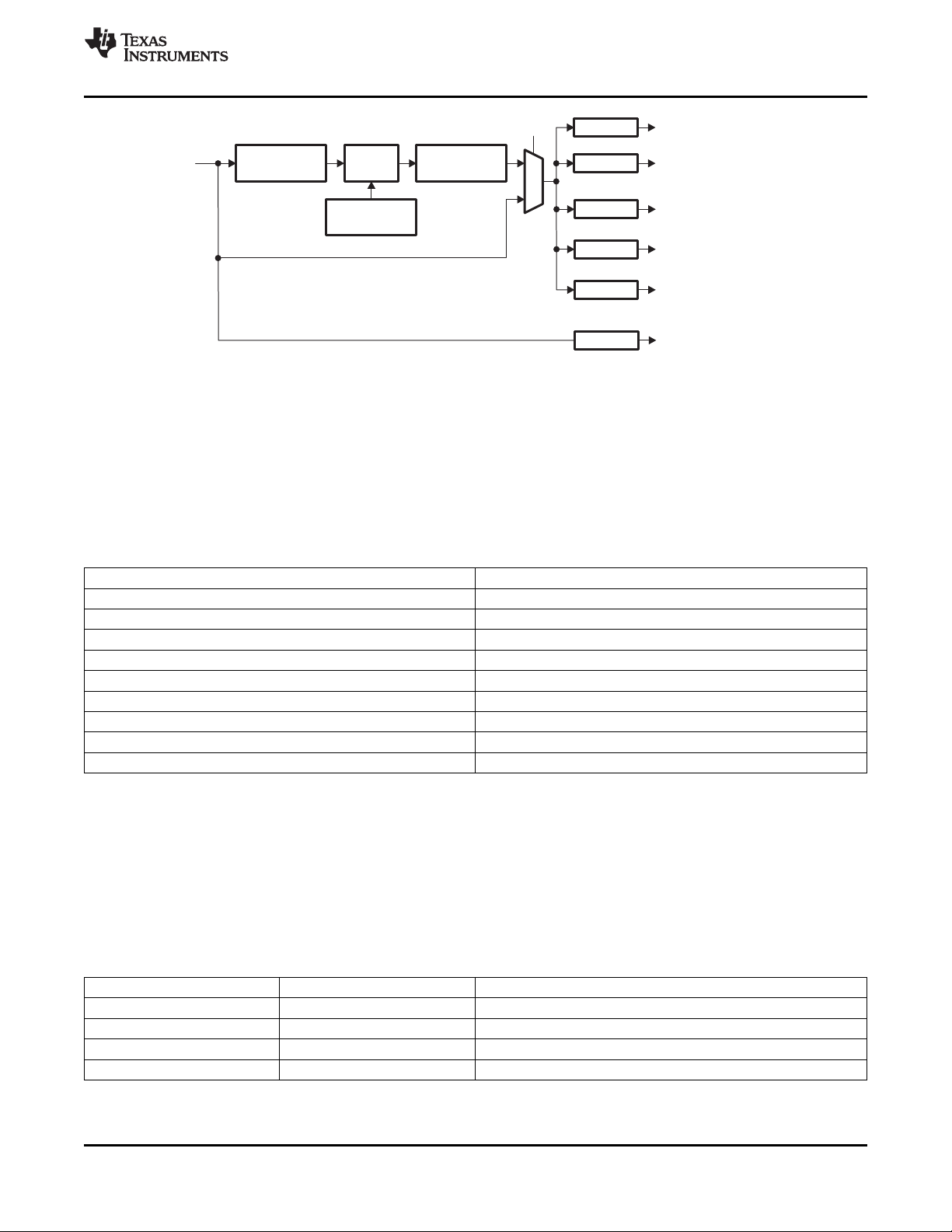
Pre-DIV
(Programmable)
PLL
1
0
PLLEN
PLLM
(Programmable)
Post-DIV*
OSCIN
PLLDIV1*
SYSCLK1
(USBReferenceClock)
PLLDIV2*
SYSCLK2(ARM926EJ-S,
HDVICP BlockClock)
PLLDIV3*
SYSCLK3(DDR2xClock)
PLLDIV4*
SYSCLK4
(VoiceCodecClock)
PLLDIV5*
SYSCLK5(VENCClock)
OSCDIV1*
OBSCLK
(CLKOUT1)
* – Programmable
TMS320DM368
www.ti.com
SPRS668B–APRIL 2010–REVISED NOVEMBER 2010
Figure 3-4. PLLC2 Configuration
3.3.5 Processing, Video, EDMA and DDR EMIF Subsystems Maximum Operating Frequencies
Table 3-4 shows the maximum speeds supported for each of the major blocks supported on the different
speed grade devices.
Table 3-4. Processing, Video, EDMA and DDR EMIF Subsystems Maximum Operating Frequencies
DM368
ARM926 RISC 432 MHz
Co-Processor (HDVICP) 340 MHz
Co-Processor (MJCP) 340 MHz
DDR2 340 MHz
mDDR 168 MHz
VPSS Logic Block 340 MHz
Peripheral System Bus and EDMA 170 MHz
VPBE-VENC 74.25 MHz
VPFE 120 MHz
3.3.6 PLL Controller Clocking Configurations Examples
Like the DM365, the DM368 uses two PLLs to generate the two fundamental clocks used on the device.
These two clocks feed two divider blocks which generate all of the functional clocks used by the
peripherals and cores in the DM368. The ARM926 and DDR peripheral in the DM368 are limited to a
maximum clock frequency of 432 MHz and 340 MHz respectively. There are some peripheral clocks on
the DM368 which are required to operate at a specific frequency by functional specification or convention.
These frequencies are detailed in Table 3-5.
Table 3-5. Specific Peripheral Operating Frequencies
VENC (standard definition) 27 required to generate a valid NTSC signal
Clock Required Frequency (MHz) Reason
VENC (high definition) 74.25 required to generate a valid ATSC signal
USB 36, 24, or 19.2 required by the USB peripheral to generate a 48 MHz USB clock
Voice Codec 4.096 required to generate a precise 16 kHz audio sample rate
Copyright © 2010, Texas Instruments Incorporated Device Configurations 59
Submit Documentation Feedback
Product Folder Link(s): TMS320DM368
Page 60
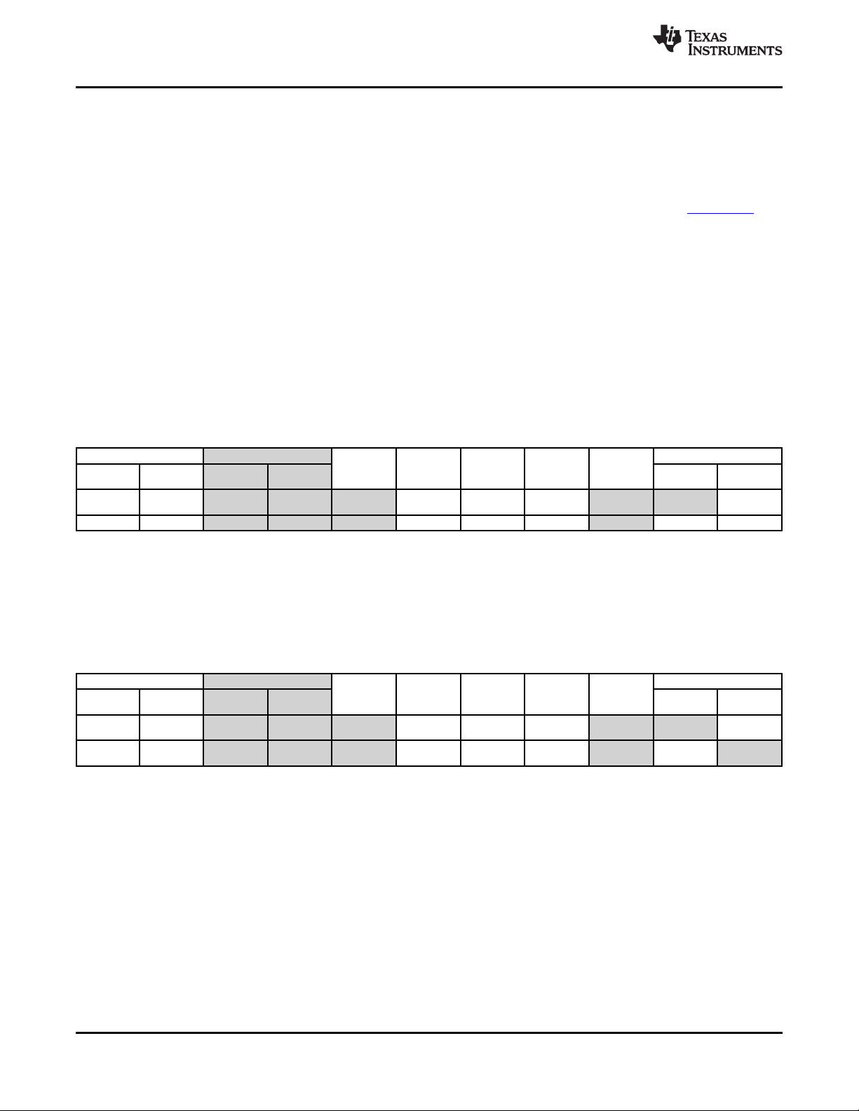
TMS320DM368
SPRS668B–APRIL 2010–REVISED NOVEMBER 2010
www.ti.com
While it is possible to generate both a 432 MHz and 340 MHz clock with the two PLLs, these two
frequencies cannot be divided down to generate all required frequencies from Table 3-5. Several different
frequency solutions are required to cover all of these requirements. The different solutions for different
input crystal frequencies are listed in the tables below.
The following tables show examples of the PLL combinations that can be supported with DM368. Please
see the TMS320DM36x DMSoC ARM Subsystem Reference Guide (literature number SPRUFG5) for
additional details on special peripherals clocking considerations and for additional PLL controller
configuration details.
There are several important points to note from these tables.
• A 432 MHz functional clock will result in DM368 voice codec sampling frequency of 16.07KHz. The
difference of 0.4375% versus 16KHz specification should be acceptable for the majority of audio
applications. If the DM368 voice codec is required to operate at precisely 16 kHz then the functional
clock can be reduced to achieve precisely that sample frequency but the ARM926 and HDVICP will
have to run at a reduced rate resulting in lower video performance.
• If a 24 MHz input crystal is used it is not possible to generate a 74.25 MHz HD video output clock.
• If a 19.2 MHz input crystal is used it is not possible to generate a valid 74.25 MHz HD output clock.
Table 3-6. 24-MHz Input Crystal Example
PLL1 PLL2 ARM DDR MJCP HDVICP Voice Codec
PLL Output (2M/(N+1)) PLL Output (2M/(N+1)) 27MHz 74.25MHz
(5)
(MHz) (MHz)
680 170/6 432 18/1 432 340 340 340 1/105 (16.06 1/16 -
680 170/6 430.08 448/25 430.08 340 340 340 1/105 - -
(1) M = PLL controller multiplier. N = PLL controller divider.
(2) All shaded frequencies derive from the PLL2 controller.
(3) PLLC1SYSCLK4 (Configuration bus clock, peripheral system interfaces, EDMA) should be half of the PLLC1SYSCLK3 (MJCP and
HDVICP bus interface clock).
(4) The Voice Codec divider value is the combination of the PLL controller 2 SYSCLK4 and Peripheral Clock Control Register PLLDIV2 bit
setting divider.
(5) PLL Output is calculated by = Oscillator Input * (2M/(N+1)).
(1) (2) (3)
kHz)
(4)
Video Encoder
Table 3-7. 36-MHz Input Crystal Example
PLL1 PLL2 ARM DDR MJCP HDVICP Voice Codec
PLL Output
680 510/27 432 12/1 432 340 340 340 1/105 (16.07 1/16 -
680 680/27 371.25 330/32 371.25 340 340 340 1/91 (15.936 - 1/5
(5)
(MHz) (MHz)
(2M/(N+1)) PLL Output (2M/(N+1)) 27MHz 74.25MHz
(1) (2) (3)
kHz)
kHz)
(4)
Video Encoder
(1) M = PLL controller multiplier. N = PLL controller divider.
(2) All shaded frequencies derive from the PLL2 controller.
(3) PLLC1SYSCLK4 (Configuration bus clock, peripheral system interfaces, EDMA) should be half of the PLLC1SYSCLK3 (MJCP and
HDVICP bus interface clock).
(4) The Voice Codec divider value is the combination of the PLL controller 2 SYSCLK4 and Peripheral Clock Control Register PLLDIV2 bit
setting divider.
(5) PLL Output is calculated by = Oscillator Input * (2M/(N+1)).
60 Device Configurations Copyright © 2010, Texas Instruments Incorporated
Submit Documentation Feedback
Product Folder Link(s): TMS320DM368
Page 61
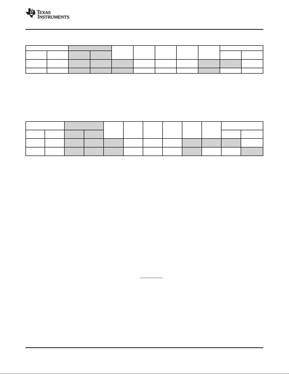
TMS320DM368
www.ti.com
Table 3-8. 19.2-MHz Input Crystal Example
PLL1 PLL2 ARM DDR MJCP HDVICP Voice Codec
PLL Output
679.82 956/27 432 90/4 432 339.91 339.91 339.91 1/105(16.07 1/16 -
679.82 956/27 430.08 112/5 430.08 339.91 339.91 339.91 1/105 - -
(1) M = PLL controller multiplier. N = PLL controller divider.
(2) All shaded frequencies derive from the PLL2 controller.
(3) PLLC1SYSCLK4 (Configuration bus clock, peripheral system interfaces, EDMA) should be half of the PLLC1SYSCLK3 (MJCP and
(4) The Voice Codec divider value is the combination of the PLL controller 2 SYSCLK4 and Peripheral Clock Control Register PLLDIV2 bit
(5) PLL Output is calculated by = Oscillator Input * (2M/(N+1)).
(5)
(MHz) (MHz)
HDVICP bus interface clock).
setting divider.
(2M/(N+1)) PLL Output (2M/(N+1)) 27MHz 74.25MHz
Table 3-9. 27-MHz Input Crystal Example
PLL1 PLL2 ARM DDR MJCP HDVICP Voice Codec USB Video
PLL Output
680 680/27 432 16/1 432 340 340 340 1/105 (16.07 1/18 1/16 -
680 680/27 371.25 110/8 371.25 340 340 340 1/91 (15.936 - - 1/5
(1) M = PLL controller multiplier. N = PLL controller divider.
(2) All shaded frequencies derive from the PLL2 controller.
(3) PLLC1SYSCLK4 (Configuration bus clock, peripheral system interfaces, EDMA) should be half of the PLLC1SYSCLK3 (MJCP and
(4) The Voice Codec divider value is the combination of the PLL controller 2 SYSCLK4 and Peripheral Clock Control Register PLLDIV2 bit
(5) PLL Output is calculated by = Oscillator Input * (2M/(N+1)).
(5)
(MHz) (MHz)
HDVICP bus interface clock).
setting divider.
(2M/(N+1)) PLL Output (2M/(N+1)) 27 MHz 74.25MHz
SPRS668B–APRIL 2010–REVISED NOVEMBER 2010
(1) (2)(3)
(4)
kHz)
(1) (2)(3)
(4)
kHz)
kHz)
Video Encoder
Encoder
For maximum H.264 encode performance the ARM must run at 432 MHz and the DDR at 340 MHz. Any
speed decrease to either of these will reduce encode performance. This means that if the ARM speed
must be reduced to enable another function it will impact the encode performance.
If USB is required then a 36 MHz, 24 MHz or 19.2 MHz input crystal is preferred as those can support
USB at full ARM rate.
If a video output is needed then a 36 MHz, 27 MHz or 24 MHz input crystal should be used. For HD video
output it may be preferred to use the EXTCLK input to inject an external 74.25 MHz clock and at the same
time operate the ARM at 432 MHz.
3.3.7 Peripheral Clocking Considerations
The device supports several peripherals with special clocking considerations (VPBE, USB, Key Scan,
ADC, Voice Codec, MJCP, HDVICP, AUXCLK, DDR2 EMIF). For more detail on these special
considerations, see the Peripheral Clocking Considerations section of theTMS320DM36x DMSoC ARM
Subsystem Reference Guide (literature number SPRUFG5).
3.4 Power and Sleep Controller (PSC)
In the device system, the Power and Sleep Controller (PSC) is responsible for managing transitions of
system power on/off, clock on/off, and reset. A block diagram of the PSC is shown in Figure 3-5. Many of
the operations of the PSC are transparent to software, such as power-on-reset operations. However, the
PSC provides you with an interface to control several important clock and reset operations.
The PSC includes the following features:
• Manages chip power-on/off, clock on/off, and resets
• Provides a software interface to:
– Control module clock ON/OFF
Copyright © 2010, Texas Instruments Incorporated Device Configurations 61
Submit Documentation Feedback
Product Folder Link(s): TMS320DM368
Page 62

arm_clock
arm_mreset
arm_power
AINTC
ARM
module_power
module_mreset
MODx
module_clock
Alwayson
domain
Interrupt
PSC
clks
PLLC
Emulation
RESETN
VDD
DMSoC
TMS320DM368
SPRS668B–APRIL 2010–REVISED NOVEMBER 2010
– Control module resets
• Supports IcePick emulation features: power, clock, and reset
Figure 3-5. Power and Sleep Controller (PSC)
www.ti.com
For more information on the PSC, see the TMS320DM36x DMSoC ARM Subsystem Reference Guide
(literature number SPRUFG5).
62 Device Configurations Copyright © 2010, Texas Instruments Incorporated
Submit Documentation Feedback
Product Folder Link(s): TMS320DM368
Page 63

TMS320DM368
www.ti.com
SPRS668B–APRIL 2010–REVISED NOVEMBER 2010
3.5 Pin Multiplexing
The device makes extensive use of pin multiplexing to accommodate the large number of peripheral
functions in the smallest possible package. In order to accomplish this, pin multiplexing is controlled using
a combination of hardware configuration (at device reset) and software control. No attempt is made by the
hardware to ensure that the proper pin muxing has been selected for the peripherals or interface mode
being used, thus proper pin muxing configuration is the responsibility of the board and software designers.
An overview of the pin multiplexing is shown in Table 3-10.
All pin multiplexing options are configurable by software via pin mux registers that reside in the System
Control Module. The PinMux0 Register controls the Video In muxing, PinMux1 register controls Video Out
signals, PinMux2 register controls AEMIF signals, PinMux3 registers control the multiplexing of the GIO
signals, the PinMux4 register controls the SPI and MMC/SD0 signals. See the TMS320DM36x DMSoC
ARM Subsystem Reference Guide (literature number SPRUFG5) for complete descriptions of the pin mux
registers.
The device configuration pins are multiplexed with AEMIF pins. Note that the AECFG[2:0] inputs only
select the default AEMIF address pin muxing. The number of active address pins may be increased or
reduced at any time by modifying the appropriate bits in the PinMux2 control register. After the device
configuration pins are sampled at reset, they automatically change to function as AEMIF pins. For more
details on AEMIF default configuration, see Section 3.7.5.
Table 3-10. Peripheral Pin Mux Overview
Peripheral Muxed With Primary Function Secondary Function Tertiary Function
VPFE (video in) GPIO and SPI3 GPIO VPFE (video in) SPI3
VPBE (video out) GPIO, PWM, and RTO GPIO VPBE (video out) PWM & RTO
AEMIF GPIO AEMIF GPIO
McBSP GPIO GPIO McBSP
MMC/SD0 MMC/SD0
MMC/SD1 GPIO and EMIF GPIO MMC/SD1 EMIF
CLKOUT GPIO GPIO CLKOUT
I2C GPIO GPIO I2C
UART0/UART1 GPIO GPIO UART
SPI0,SPI1,SPI2,SPI4 GPIO GPIO SPI
EMAC GPIO GPIO EXTINT EMAC
HPI AEMIF AEMIF HPI
Copyright © 2010, Texas Instruments Incorporated Device Configurations 63
Submit Documentation Feedback
Product Folder Link(s): TMS320DM368
Page 64

TMS320DM368
SPRS668B–APRIL 2010–REVISED NOVEMBER 2010
3.6 Device Reset
There are five types of reset. The types of reset differ by how they are initiated and/or by their effect on
the chip. Each type is briefly described in Table 3-11 and further described in the TMS320DM36x DMSoC
ARM Subsystem Reference Guide (literature number SPRUFG5).
Table 3-11. Reset Types
Type Initiator Effect
POR (Power-On-Reset) RESET pin low and TRST low Total reset of the chip (cold reset).
Activates the POR signal on chip, which is used to reset
test/emulation logic.
Warm Reset RESET pin low Resets everything except for test/emulation logic.
ARM emulator stays alive during Warm reset.
Max Reset ARM emulator or Watchdog Timer Same effect as warm reset.
(WDT)
System Reset ARM emulator A soft reset.
Soft reset maintains memory contents, and does not affect or reset
clocks or power states.
Module Reset ARM software Can independently apply reset to each module, via an MMR.
Intended as a debug tool, and not necessarily for general use.
3.7 Default Device Configurations
After POR, warm reset, and max reset, the chip is in its default configuration. This section highlights the
default configurations associated with PLLs, clocks, ARM boot mode, and AEMIF.
www.ti.com
Note: Default configuration is the configuration immediately after POR, warm reset, and max reset and
just before the boot process begins. The boot ROM updates the configuration. See Section 3.2 for more
information on the boot process.
3.7.1 Device Configuration Pins
The device configuration pins are described in Table 3-12. The device configuration pins are latched at
reset and allow you to configure all of the following options at reset:
• ARM Boot Mode
• Asynchronous EMIF pin configuration
These pins are described further in the following sections.
Note: The device configuration pins are multiplexed with AEMIF pins. After the device configuration pins
are sampled at reset, they automatically change to function as AEMIF pins. Pin multiplexing is described
in Section 3.5.
Table 3-12. Device Configuration
Device Configuration Input Function Pin pull-down)
BTSEL[2:0] Selects ARM boot mode EM_A[13:11] 000
AECFG[2:0] AEMIF Configuration
000 = Boot from ROM (NAND) (Boot from ROM - NAND)
001 = Boot from AEMIF
010 = Boot from ROM (MMC/SD)
011 = Boot from ROM (UART)
100 = Boot from ROM (USB)
101 = Boot from ROM (SPI)
110 = Boot from ROM (EMAC)
111 = Boot from ROM (HPI)
(1)
AECFG[2] = '0' for 8-bit AEMIF configuration (8-bit NAND)
AECFG[2] = '1' for 16-bit AEMIF configuration
Sampled pull-up/
EM_A[10:8] 000
Default Setting (by internal
(1) Other supported AECFG[2:0] combinations can be found in Table 3-14.
64 Device Configurations Copyright © 2010, Texas Instruments Incorporated
Submit Documentation Feedback
Product Folder Link(s): TMS320DM368
Page 65

TMS320DM368
www.ti.com
SPRS668B–APRIL 2010–REVISED NOVEMBER 2010
Table 3-12. Device Configuration (continued)
Device Configuration Input Function Pin pull-down)
OSCCFG Oscillator Configuration GIO81 0
OSCCFG = '0' for mode #1 (Mode #1)
OSCCFG = '1' for mode #2
Sampled pull-up/
Default Setting (by internal
3.7.2 PLL Configuration
After POR, warm reset, and max reset, the PLLs and clocks are set to their default configurations. The
PLLs are in bypass mode and disabled by default. This means that the input reference clock at MXI1
(typically 24 MHz) drives the chip after reset. For more information on device clocking, see Section 3.3 .
The default state of the PLLs is reflected in the default state of the register bits in the PLLC registers.
Refer to the TMS320DM36x DMSoC ARM Subsystem Reference Guide (literature number SPRUFG5).
3.7.3 Power Domain and Module State Configuration
Only a subset of modules are enabled after reset by default. Table 3-13 shows which modules are
enabled after reset. Table 3-13 shows that the following modules are enabled depending on the sampled
state of the device configuration pins. For example, if UART boot mode is BTSEL[2:0] = 011, then the
default state of the UART module is enabled. For more information on module configuration, refer to the
TMS320DM36x DMSoC ARM Subsystem Reference Guide (literature number SPRUFG5).
Table 3-13. LPSC Assignments and Module Configuration
(1)
LPSC/
MODULE MODULE NAME BTSEL [2:0]
NUMBER
000 001 010 011 100 101 110 111
ROM ROM ROM ROM ROM
(NAND) (UART0) (USB) (SPI0) (EMAC)
0 EDMA CC On On On On
1 EDMA TC0 On On On On
2 EDMA TC1
3 EDMA TC2
4 EDMA TC3
5 TIMER3
6 SPI1
7 MMC_SD1
8 McBSP
9 USB On
10 PWM3
11 SPI2
12 RTO
13 DDR EMIF
14 AEMIF On On
15 MMC/SD0 On
16 Reserved
17 TIMER4
18 I2C
19 UART0 On
20 UART1
21 UHPI On
(1) "(Blank)" in the above table indicates module is disabled.
Copyright © 2010, Texas Instruments Incorporated Device Configurations 65
AEMIF (MMC/SD0 ROM (HPI)
Submit Documentation Feedback
Product Folder Link(s): TMS320DM368
ROM
)
Page 66

TMS320DM368
SPRS668B–APRIL 2010–REVISED NOVEMBER 2010
Table 3-13. LPSC Assignments and Module Configuration (continued)
LPSC/
MODULE MODULE NAME BTSEL [2:0]
NUMBER
22 SPI0 On
23 PWM0
24 PWM1
25 PWM2
26 GPIO
27 TIMER0 On On On On On On On On
28 TIMER1
29 TIMER2 On On On On On On On On
30 SYSTEM On On On On On On On On
31 ARM On On On On On On On On
32 Reserved Reserved Reserved Reserved Reserved Reserved Reserved Reserved Reserved
33 Reserved Reserved Reserved Reserved Reserved Reserved Reserved Reserved Reserved
34 Reserved On On On On On On On On
35 EMULATION On On On On On On On On
36 Reserved Reserved Reserved Reserved Reserved Reserved Reserved Reserved Reserved
37 Reserved Reserved Reserved Reserved Reserved Reserved Reserved Reserved Reserved
38 SPI3
39 SPI4
40 EMAC On
41 RTC On On On On On On On On
42 KEYSCAN
43 ADC
44 Voice Codec
45 VDAC CLKREC
46 VDAC CLK
47 VPSS MASTER
48 Reserved Reserved Reserved Reserved Reserved Reserved Reserved Reserved Reserved
49 Reserved Reserved Reserved Reserved Reserved Reserved Reserved Reserved Reserved
50 MJCP
51 HDVICP
www.ti.com
3.7.4 ARM Boot Mode Configuration
The ARM can boot from either Asynchronous EMIF (OneNand/NOR) or from ARM ROM, as determined
by the setting of the device configuration pins BTSEL[2:0]. The boot selection pins (BTSEL[2:0]) determine
the ARM boot process. After reset (POR, warm reset, or max reset), ARM program execution begins in
ARM ROM at 0x0000: 8000, except when BTSEL[2:0] = 001, indicating AEMIF (OneNand/NOR) flash
boot.
Boot modes are further described in Section 3.2.
66 Device Configurations Copyright © 2010, Texas Instruments Incorporated
Submit Documentation Feedback
Product Folder Link(s): TMS320DM368
Page 67

TMS320DM368
www.ti.com
3.7.5 AEMIF Configuration
3.7.5.1 AEMIF Pin Configuration
The input pins AECFG[2:0] determine the AEMIF configuration immediately after reset. Pins that are not
assigned to another peripheral and not enabled as address signals become GPIOs. These may be used
as ALE and CLE signals for NAND Flash control if booting from internal ROM. If booting from NOR Flash
then the appropriate number of address output must be enabled by the AECFG[2:0] inputs at reset. The
enabled address signals are always contiguous from EM_BA[1] upwards; bits cannot be skipped. EM_A[0]
does not represent the lowest AEMIF address bit. The device has 23 address lines and 2 chip selects with
an 8-bit or 16-bit option. The device supports only 8-bit and 16-bit data widths for the AEMIF.
• 16-bit mode: EM_BA[1] represents the LS address bit (the half-word address) and EM_BA[0]
represents address bit (A[14]). The maximum number of address lines pins in 16-bit mode are 23,
which include EM_BA[1] + EM_A[0:13] +EM_BA[0] (as pin A[14] via PINMUX2 register) + EM_A[15:20]
+EM_A[21] (via PINMUX4 register)
Note: Pins EM_A[15:21] are available by programming the PinMux4 register in software after boot, but
must be pulled down externally so that valid voltage levels are provided on the full set of address pins
during boot time. EM_A[15:21] come out of reset as GPIO pins per the PinMux4 register.
• 8-bit mode: EM_BA[1:0] represent the 2 LS address bits. Additional selections are available by
programming the PinMux2 register in software after boot. The maximum number of address lines in
8-bit mode are 23, which include EM_BA[0:1] + EM_A[0:13] + A[14] (via PINMUX4 register) +
EM_A[15:20].
Note: Pins EM_A[15:20] are available by programming the PinMux4 register in software after boot, but
must be pulled down externally so that valid voltage levels are provided on the full set of address pins
during boot time. EM_A[15:20] come out of reset as GPIO pins per the PinMux4 register.
SPRS668B–APRIL 2010–REVISED NOVEMBER 2010
For additional details about the PinMux2 and PinMux4 registers, see the TMS320DM36x DMSoC ARM
Subsystem Reference Guide (literature number SPRUFG5).
The device's pin-mux control logic allows all of the Asynchronous EMIF address pins to be used as
GPIOs. If devices (such as NAND Flash) attached to the AEMIF require less than the 16 address pins
provided, then the unused upper-order addresses may be configured as GPIOs. These pins must be
configured at reset so that pins being driven by the AEMIF with addresses will not cause bus contention
with pins being driven by the system as general purpose inputs.
The AECFG[2:0] value does not affect the operation of the AEMIF module itself, only which of its address
bits are seen on the device pins (resulting in the natural ramifications if devices don’t receive all address
signals or if contention with general purpose inputs occurs). As shown in Table 3-14, the number of
address bits enabled on the AEMIF is selectable from 0 to 16 at boot time, see notes above for additional
support of up-to 23 address lines.
Copyright © 2010, Texas Instruments Incorporated Device Configurations 67
Submit Documentation Feedback
Product Folder Link(s): TMS320DM368
Page 68

TMS320DM368
SPRS668B–APRIL 2010–REVISED NOVEMBER 2010
Table 3-14. AECFG (Async EMIF Configuration) Coding at Boot Time
000 001 010 100 101 110
GPIO[65] EM_A[14] EM_BA[0] GPIO[65] EM_A[14] EM_BA[0]
GPIO[66] EM_BA[1] EM_BA[1] GPIO[66] EM_BA[1] EM_BA[1]
GPIO[67] EM_A[0] EM_A[0] GPIO[67] EM_A[0] EM_A[0]
EM_A[1] EM_A[1] EM_A[1] EM_A[1] EM_A[1] EM_A[1]
EM_A[2] EM_A[2] EM_A[2] EM_A[2] EM_A[2] EM_A[2]
GPIO[68] EM_A[3] EM_A[3] GPIO[68] EM_A[3] EM_A[3]
GPIO[69] EM_A[4] EM_A[4] GPIO[69] EM_A[4] EM_A[4]
GPIO[70] EM_A[5] EM_A[5] GPIO[70] EM_A[5] EM_A[5]
GPIO[71] EM_A[6] EM_A[6] GPIO[71] EM_A[6] EM_A[6]
GPIO[72] EM_A[7] EM_A[7] GPIO[72] EM_A[7] EM_A[7]
GPIO[73] EM_A[8] EM_A[8] GPIO[73] EM_A[8] EM_A[8]
GPIO[74] EM_A[9] EM_A[9] GPIO[74] EM_A[9] EM_A[9]
GPIO[75] EM_A[10] EM_A[10] GPIO[75] EM_A[10] EM_A[10]
GPIO[76] EM_A[11] EM_A[11] GPIO[76] EM_A[11] EM_A[11]
GPIO[77] EM_A[12] EM_A[12] GPIO[77] EM_A[12] EM_A[12]
GPIO[78] EM_A[13] EM_A[13] GPIO[78] EM_A[13] EM_A[13]
GPIO[57] GPIO[46] GPIO[46] EM_D[8] EM_D[8] EM_D[8]
GPIO[58] GPIO[47] GPIO[47] EM_D[9] EM_D[9] EM_D[9]
GPIO[59] GPIO[48] GPIO[48] EM_D[10] EM_D[10] EM_D[10]
GPIO[60] GPIO[49] GPIO[49] EM_D[11] EM_D[11] EM_D[11]
GPIO[61] GPIO[50] GPIO[50] EM_D[12] EM_D[12] EM_D[12]
GPIO[62] GPIO[51] GPIO[51] EM_D[13] EM_D[13] EM_D[13]
GPIO[63] GPIO[52] GPIO[52] EM_D[14] EM_D[14] EM_D[14]
GPIO[64] GPIO[53] GPIO[53] EM_D[15] EM_D[15] EM_D[15]
www.ti.com
3.7.5.2 AEMIF Timing Configuration
When AEMIF is enabled, the wait state registers are reset to the slowest possible configuration, which is
88 cycles per access (16 cycles of setup, 64 cycles of strobe, and 8 cycles of hold). Thus, with a 24 MHz
clock at MXI/MXO, the AEMIF is configured to run at (12 MHz/ 88) which equals approximately 136.36
kHz.
3.7.6 Oscillator Frequency Configuration
The oscillator input pins, MXI1, MXO, are designed to operate in two frequency ranges depending on the
GIO81(OSCCFG) pin sampled at reset, which should be set according to the required input frequency of
operation. See Table 3-15 for details.
Table 3-15. Operation Frequency
MODE GIO81 (OSCCFG) OSCILLATION
1 0 15 - 35MHz
2 1 30 - 40MHz
The frequency selection pin cannot be changed dynamically while the oscillator is running. They should
only be set once before oscillator startup.
The GIO81(OSCCFG) state is latched during reset, and it specifies the oscillation frequency mode as
shown in Table 3-15.
68 Device Configurations Copyright © 2010, Texas Instruments Incorporated
Submit Documentation Feedback
Product Folder Link(s): TMS320DM368
Page 69

TMS320DM368
www.ti.com
3.8 Debugging Considerations
3.8.1 Pullup/Pulldown Resistors
Proper board design should ensure that input pins to the DMSoC device always be at a valid logic level
and not floating. This may be achieved via pullup/pulldown resistors. The DMSoC features internal pullup
(IPU) and internal pulldown (IPD) resistors on most pins to eliminate the need, unless otherwise noted, for
external pullup/pulldown resistors.
An external pullup/pulldown resistor needs to be used in the following situations:
• Boot and Configuration Pins: If the pin is both routed out and 3-stated (not driven), an external
pullup/pulldown resistor is strongly recommended, even if the IPU/IPD matches the desired
value/state.
• Other Input Pins: If the IPU/IPD does not match the desired value/state, use an external
pullup/pulldown resistor to pull the signal to the opposite rail.
For the boot and configuration pins, if they are both routed out and 3-stated (not driven), it is strongly
recommended that an external pullup/pulldown resistor be implemented. Although, internal
pullup/pulldown resistors exist on these pins and they may match the desired configuration value,
providing external connectivity can help ensure that valid logic levels are latched on these device boot and
configuration pins. In addition, applying external pullup/pulldown resistors on the boot and configuration
pins adds convenience to the user in debugging and flexibility in switching operating modes.
Tips for choosing an external pullup/pulldown resistor:
• Consider the total amount of current that may pass through the pullup or pulldown resistor. Make sure
to include the leakage currents of all the devices connected to the net, as well as any internal pullup or
pulldown resistors.
• Decide a target value for the net. For a pulldown resistor, this should be below the lowest VILlevel of
all inputs connected to the net. For a pullup resistor, this should be above the highest VIHlevel of all
inputs on the net. A reasonable choice would be to target the VOLor VOHlevels for the logic family of
the limiting device; which, by definition, have margin to the VILand VIHlevels.
• Select a pullup/pulldown resistor with the largest possible value; but, which can still ensure that the net
will reach the target pulled value when maximum current from all devices on the net is flowing through
the resistor. The current to be considered includes leakage current plus, any other internal and
external pullup/pulldown resistors on the net.
• For bidirectional nets, there is an additional consideration which sets a lower limit on the resistance
value of the external resistor. Verify that the resistance is small enough that the weakest output buffer
can drive the net to the opposite logic level (including margin).
• Remember to include tolerances when selecting the resistor value.
• For pullup resistors, also remember to include tolerances on the DVDDrail.
SPRS668B–APRIL 2010–REVISED NOVEMBER 2010
For most systems, a 1-kΩ resistor can be used to oppose the IPU/IPD while meeting the above criteria.
Users should confirm this resistor value is correct for their specific application.
For most systems, a 20-kΩ resistor can be used to compliment the IPU/IPD on the boot and configuration
pins while meeting the above criteria. Users should confirm this resistor value is correct for their specific
application.
For more detailed information on input current (II), and the low-/high-level input voltages (VILand VIH) for
the device, see Section 5.2, Recommended Operating Conditions.
For the internal pullup/pulldown resistors for all device pins, see the peripheral/system-specific terminal
functions table.
Copyright © 2010, Texas Instruments Incorporated Device Configurations 69
Submit Documentation Feedback
Product Folder Link(s): TMS320DM368
Page 70

TMS320DM368
SPRS668B–APRIL 2010–REVISED NOVEMBER 2010
4 System Interconnect
The device uses a 64-bit crossbar architecture to control access between device processors, subsystems
and peripherals. There are eleven transfer masters (TCs have separate read and write connections)
connected to the crossbar; ARM, the Video Processing Subsystem (VPSS), the master peripherals (USB,
EMAC, HPI), and four EDMA transfer controllers. These can be connected to seven separate slave ports;
ARM, the DDR EMIF, CFG bus peripherals, MJCP, and HDVICP. Not all masters may connect to all
slaves. Connection paths are indicated by √ at intersection points shown in Table 4-1.
Table 4-1. System Connection Matrix
SLAVE MODULE
DMA ARM Internal MPEG/JPEG HD Video Image Config Bus Registers DDR EMIF
Master Memory Coprocessor Coprocessor and Memory
Memory Memory Memory
ARM √ √ √ √ √
VPSS √ √
DMA Master Peripherals √ √
(USB, EMAC, HPI)
EDMA3TC0 √ √ √ √ √
EDMA3TC1 √ √ √ √ √
EDMA3TC2 √ √ √ √ √
EDMA3TC3 √ √ √ √ √
www.ti.com
70 System Interconnect Copyright © 2010, Texas Instruments Incorporated
Submit Documentation Feedback
Product Folder Link(s): TMS320DM368
Page 71

TMS320DM368
www.ti.com
SPRS668B–APRIL 2010–REVISED NOVEMBER 2010
5 Device Operating Conditions
5.1 Absolute Maximum Ratings Over Operating Case Temperature Range (Unless Otherwise Noted)
Supply voltage ranges All 1.8 V supplies -0.3 V to 2.45 V
Input voltage ranges All 3.3 V I/Os -0.5 V to 3.8 V
Operating case temperature ranges
Storage temperature ranges T
(1) Stresses beyond those listed under "absolute maximum ratings" may cause permanent damage to the device. These are stress ratings
only, and functional operation of the device at these or any other conditions beyond those indicated under "recommended operating
conditions" is not implied. Exposure to absolute-maximum-rated conditions for extended periods may affect device reliability.
(2) All voltage values are with respect to V
(1) (2)
SS.
All 1.35-V supplies -0.3 V to 1.6 V
All 3.3 V supplies -0.3 V to 3.8 V
All 1.8 V I/Os -0.5 V to 2.6 V
USB_VBUS 0 V to 5.5 V
Commercial Temperature T
Extended Temperature [D version devices] T
stg
c
c
0°C to 85 °C
-40°C to 85 °C
-55°C to 150°C
Copyright © 2010, Texas Instruments Incorporated Device Operating Conditions 71
Submit Documentation Feedback
Product Folder Link(s): TMS320DM368
Page 72

TMS320DM368
SPRS668B–APRIL 2010–REVISED NOVEMBER 2010
5.2 Recommended Operating Conditions
NAME DESCRIPTION MIN NOM MAX UNIT
Supply
Voltage
Supply
Ground
Voltage Input
High
C
VDD
V
DD12_PRTCSS
V
DDA12_DAC
(1)
V
PP
V
DDS18
V
DD18_PRTCSS
V
DDMXI
V
DD18_DDR
V
DDA18_PLL
V
DDA18_USB
V
DDA18_VC
V
DDA18_USB
V
DDA18_ADC
V
DDA18_DAC
V
DD_AEMIF1_18_33
V
DD_AEMIF2_18_33
V
DD_ISIF18_33
V
DDS33
V
DDA33_USB
V
DDA33_VC
V
SS
V
SS_MX1
V
SS_32K
V
SSA
V
SSA18_USB
V
SSA33_USB
V
SSA33_VC
V
SSA18_VC
V
SSA_ADC
V
SSA18_DAC
V
SSA12_DAC
V
IH
Core Supply Voltage 432-MHz devices 1.28 1.35 1.42 V
PRTCSS Oscillator and
PRTCSS Core Supply Voltage
1.2-V DAC Supply Voltage 432-MHz devices 1.28 1.35 1.42 V
VPP Supply Voltage 432-MHz devices 1.28 1.35 1.42 V
1.8-V Supply Voltage
1.8-V PWR CTRL Supply Voltage
1.8-V System Oscillator Supply Voltage
1.8-V DDR2 Supply Voltage
1.8-V PLL Supply Voltage
1.8-V USB Supply Voltage
1.8-V Voice CODEC Supply Voltage
1.8-V USB Supply Voltage
1.8-V ADC Supply Voltage
1.8-V DAC Supply Voltage
1.8/3.3-V switchable EMIF1 Supply Voltage
1.8/3.3-V switchable EMIF2 Supply Voltage 1.71/3.14 1.8/3.3 1.89/3.46 V
1.8/3.3-V switchable ISIF Supply Voltage
3.3-V Supply Voltage
3.3-V USB Supply Voltage 3.14 3.3 3.46 V
3.3-V Voice CODEC Supply Voltage
Core, USB Digital ground
OSC (MX1) ground
OSC (32K) ground
PLL ground
(2)
(2)
(3)
USB ground
3.3-V USB ground 0 0 0 V
3.3-V Voice CODEC ground
1.8-V Voice CODEC ground
ADC ground
1.8-V DAC ground
1.2-V DAC ground
High-level input voltage
(4)
, excludes switchable I/O
(3.3V I/O)
High-level input voltage, non-DDR2 I/O, excludes switchable I/O
(1.8V I/O)
www.ti.com
432-MHz devices 1.28 1.35 1.42 V
1.71 1.8 1.89 V
2 V
0.7V
DDS18
V
(1) For proper device operation, this pin must always be connected to C
(2) Oscillator ground must be kept separate from other grounds and connected directly to the crystal load capacitor ground (see
VDD
.
Section 6.6.1).
(3) For proper device operation, keep this pin separate from digital ground.
(4) These I/O specifications apply to regular 3.3 V I/Os and do not apply to DDR2/mDDR, USB I/Os. DDR2/mDDR I/Os are 1.8 V I/Os and
adhere to JESD79-2A standard, USB I/Os adhere to USB2.0 spec.
72 Device Operating Conditions Copyright © 2010, Texas Instruments Incorporated
Submit Documentation Feedback
Product Folder Link(s): TMS320DM368
Page 73

TMS320DM368
www.ti.com
SPRS668B–APRIL 2010–REVISED NOVEMBER 2010
NAME DESCRIPTION MIN NOM MAX UNIT
V
IH12RTC
V
IH1833
V
IL
High-level input voltage I/O (1.35-V)
(PWRCNT/PWRST/RTCXI/RTCXO)
HIgh-level switchable input 3.3V I/O mode 2
(4)
voltage
(VDD_AEMIF1_18_33,
VDD_AEMIF2_18_33,
VDD_ISIF_18_33 powered
(5)(6) (7)(8)
I/Os)
Low-level input voltage
(4)
1.8V I/O mode 0.7V
, excludes switchable I/O
(3.3V I/O)
Low-level input voltage
(4)
, non-DDR2 I/O, excludes switchable I/O 0.3*VDDS
(1.8V I/O) 18
Voltage Input
Low
V
IL12RTC
V
IL1833
RTC Low-level input voltage
(1.35V I/O)
Low-level switchable input 3.3V I/O mode 0.8
(4)
voltage
(VDD_AEMIF1_18_33,
VDD_AEMIF2_18_33,
VDD_ISIF_18_33 powered
(4)
1.8V I/O mode
I/Os)
V
REF
R
BIAS
HD 3CH DAC
Video Buffer
USB
Voice Codec
ADC F
Temperature T
(5) V
(6) V
(7) Example 1: V
(8) V
(9)
R
LOAD_X
C
BG
R
OUT
R
FB
(9)
R
BIAS
C
BG
USB_VBUS USB external charge pump input 0 5.25 V
V
DDA12LDO_USB
f
s
- System clock 256fskHz
SCLK
c
DD_AEMIF1_18_33
]pins, Keyscan, or GPIO pins.
DD_AEMIF2_18_33:
Keyscan, or GPIO pins.
Example 2: V
DD_ISIF_18_33
(SPI3_SCLK,SPI3_SIMO,SPI3_SCS[0], SPI3_SCS[1]) or USBDRVVBUS or GPIO pins.
: can be used as a power supply for EM_A[3:13], EM_BA0, EM_BA1, EM_CE[0], EM_ADV, EM_CLK, EM_D[8:15
can be used as a power supply for EM_A[0:2], EM_CE[1], EM_WE, EM_OE, EM_WAIT, EM_D[0:7] pins, HPI,
DD_AEMIF2_18_33
DD_AEMIF1_18_33
: can be used as a power supply for VPFE pins (CIN[7:0], YIN[7:0], C_WE_FIELD, PCLK), or SPI3
DAC reference voltage 475 500 525 mV
DAC full-scale current adjust resistor 2376 2400 2424 Ω
Output resistor 74.25 75 75.75 Ω
Bypass capacitor 0.1 uF
Output resistor (ROUT), between TVOUT and VFB pins 2128.5 2150 2171.5
Feedback resistor, between VFB and IDACOUT pins. 2079 2100 2121
Full-scale current adjust resistor 2400 Ω
Bypass capacitor 0.1 uF
Internal LDO output
(10)
Sampling frequency 8 16 kHz
SCLK frequency 2 MHz
Operating case temperature
range
at 1.8-V for 8-bit NAND V
and V
DD_AEMIF2_18_33
at 1.8-V for 16-bit NAND.
Default Temperature 0 85 °C
Extended Temperature [D version
devices]
DD_AEMIF1_18_33
at 3.3-V for GPIO.
(9) See Section 6.12.2.4. Also, resistors should be E-96 spec line (3 digits with 1% accuracy).
(10) For proper device operation, this pin must be connected to a 0.22mF capacitor to V
DDA12LDO_USB
0.75*VDD
12_PRTC V
SS
DDS18
0.8 V
0.25*VDD
12_PRTC V
SS
0.3*VDDS
18
0.22 µF
-40 85 °C
.
V
V
V
Ω
Copyright © 2010, Texas Instruments Incorporated Device Operating Conditions 73
Submit Documentation Feedback
Product Folder Link(s): TMS320DM368
Page 74

TMS320DM368
SPRS668B–APRIL 2010–REVISED NOVEMBER 2010
www.ti.com
5.3 Electrical Characteristics Over Recommended Ranges of Supply Voltage and Operating Case Temperature (Unless Otherwise Noted)
PARAMETER TEST CONDITIONS
High-level output voltage
(3.3V I/O)
V
OH
High-level output voltage
(3.3V I/O)
High-level output voltage V
Voltage
Output
(2)
(1.8V I/O) 0.45
Low-level output voltage
(3.3V I/O)
V
OL
Low-level output voltage
(3.3V I/O)
Low-level output voltage
(1.8V I/O)
I
I
I
I(pullup)
Current
Input/Output
Capacitance pF
I
I(pulldown)
I
OH
I
OL
(5)
I
OZ
C
I
C
O
Input current for I/O without
internal pull-up/pull-down
Input current for I/O with
internal pull-up
Input current for I/O with
internal pull-down
(3) (4)
(3) (4)
High-level output current All peripherals -4000
Low-level output current All peripherals 4000
I/O off-state output current ±20
Input capacitance 4
Output capacitance 4
V
= MIN, IOH= -2mA 2.4
DDS33
V
= MIN, IOH= -100mA 2.94 V
DDS33
V
= MIN, IOH= -2mA
DDS18
V
= MIN, IOL= 2mA 0.4
DDS33
V
= MIN, IOL= 100mA 0.2 V
DDS33
V
= MIN, IOH= 2mA 0.45
DDS18
VI= VSSto V
VI= VSSto V
VI= VSSto V
VO= VDDor V
(internal pull disabled)
DD
DD
DD
SS
Resolution Resolution 10 Bits
R
= 75 Ω
LOAD
(video buffer disabled)
R
= 75 Ω
LOAD
(video buffer disabled)
LOAD
HD 3CH
DAC
INL Integral non-linearity, best fit -1.5 1.5 LSB
DNL Differential non-linearity -1 1 LSB
V
OUT
Z
SET
Output compliance range IFS = 6.67 mA, R
Zero Scale Offset Error 0.5 %
G_ERR Gain Error -5 5 %
Ch_match Channel matching +/-2 %
Output high voltage
(top of 75% NTSC or PAL colorbar)
Output low voltage
(bottom of sync tip)
Video Buffer
V
OH(VIDBUF)
V
OL(VIDBUF)
RES Resolution 10 bits
V
OUT
Output Voltage R
= 75 Ω 0.35 1.35 V
LOAD
(1)
MIN TYP MAX UNIT
-
DDS18
100
-100
= 75 Ω 0 V
1.35
0.35
±10
REF
mA
V
V
(1) For test conditions shown as MIN, MAX, or NOM, use the appropriate value specified in the recommended operating conditions table.
(2) These I/O specifications apply to regular 3.3 V and 1.8V I/Os and do not apply to DDR2/mDDR, USB I/Os. DDR2/mDDR I/Os are 1.8 V
I/Os and adhere to JESD79-2A standard, USB I/Os adhere to USB2.0 spec.
(3) This specification applies only to pins with an internal pullup (PU) or pulldown (PD). See or Section 2.8 for pin descriptions.
(4) To pull up a signal to the opposite supply rail, a 1 kΩ resistor is recommended.
(5) IOZapplies to output only pins, indicating off-state (Hi-Z) output leakage current.
74 Device Operating Conditions Copyright © 2010, Texas Instruments Incorporated
Submit Documentation Feedback
Product Folder Link(s): TMS320DM368
Page 75

TMS320DM368
www.ti.com
Voice
Codec
ADC
SPRS668B–APRIL 2010–REVISED NOVEMBER 2010
PARAMETER TEST CONDITIONS
(1)
MIN TYP MAX UNIT
MIC in to ADC (gain = 20 dB)
V
mic
Full scale input 0.063 Vrms
GeAD Gain error 0 dB
V
com
Common voltage 0.9 V
THD + N -1db, 1kHz -62 dB
DNR A-weighted 70 dB
SNR A-weighted 67 dB
Input resistance 10 kΩ
Input capacitance 10 pF
DAC-to-Line Output
Full scale output 0.8 Vrms
Gain error 0 dB
Common voltage 1.5 V
THD + N -60 dB
DNR A-weighted 70 dB
SNR A-weighted 70 dB
Load resistance 10 kΩ
Load capacitance 20 pF
DAC-to-Speaker Output
Output power RL= 8Ω, THD = 10% 240 mW
Output noise A-weighted 120 mVrms
Load resistance 8 Ω
Load capacitance 50 pF
Decimation filter in ADC
Pass band 0.375f
s
kHz
Pass band ripple +/- 0.2 dB
Stop band 0.562f
s
kHz
Stop band attenuation 40 dB
HPF cutoff frequency 1.25mfs Hz
Interpolation filter in DAC
Pass band 0.437f
s
kHz
Pass band ripple +/- 0.2 dB
Stop band 0.562f
s
kHz
Stop band attenuation 40 dB
DNL Static differential non-linearity error F
INL Static integral non-linearity error F
Z
SET
F
SET
Zero scale offset error -6 6 LSB
Full scale offset error -6 6 LSB
= 2MHz -1 2.5 LSB
SCLK
= 2MHz -3 3 LSB
SCLK
Copyright © 2010, Texas Instruments Incorporated Device Operating Conditions 75
Submit Documentation Feedback
Product Folder Link(s): TMS320DM368
Page 76
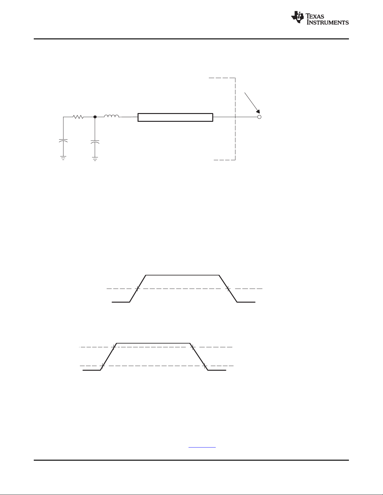
TransmissionLine
4.0pF 1.85pF
Z0=50 Ω
(seenote)
Tester PinElectronics
Data SheetTimingReferencePoint
Output
Under
Test
42 Ω 3.5nH
DevicePin
(seenote)
V
ref
V
ref
=VILMAX(orVOLMAX)
V
ref
=VIHMIN(orVOHMIN)
TMS320DM368
SPRS668B–APRIL 2010–REVISED NOVEMBER 2010
6 Peripheral Information and Electrical Specifications
6.1 Parameter Information Device-Specific Information
A. The data sheet provides timing at the device pin. For output timing analysis, the tester pin electronics and its
transmission line effects must be taken into account. A model of the tester pin electronics is shown in Figure 6-1. A
transmission line with a delay of 2 ns or longer can be used to produce the desired transmission line effect. The
transmission line is intended as a load only. It is not necessary to add or subtract the transmission line delay (2 ns or
longer) from the data sheet timings.
Input requirements in this data sheet are tested with an input slew rate of < 4 Volts per nanosecond (4 V/ns) at the
device pin and the input signals are driven between 0V and the appropriate I/O supply for the signal.
Figure 6-1. Test Load Circuit for AC Timing Measurements
www.ti.com
The load capacitance value stated is only for characterization and measurement of AC timing signals. This
load capacitance value does not indicate the maximum load the device is capable of driving.
6.1.1 Signal Transition Levels
All input and output timing parameters are referenced to V
V
= 1.65 V. For 1.8 V I/O, V
ref
= 0.9 V.
ref
Figure 6-2. Input and Output Voltage Reference Levels for AC Timing Measurements
All rise and fall transition timing parameters are referenced to VILMAX and VIHMIN for input clocks,
VOLMAX and VOHMIN for output clocks.
Figure 6-3. Rise and Fall Transition Time Voltage Reference Levels
6.1.2 Timing Parameters and Board Routing Analysis
for both "0" and "1" logic levels. For 3.3 V I/O,
ref
The timing parameter values specified in this data sheet do not include delays by board routings. As a
good board design practice, such delays must always be taken into account. Timing values may be
adjusted by increasing/decreasing such delays. TI recommends utilizing the available I/O buffer
information specification (IBIS) models to analyze the timing characteristics correctly. To properly use IBIS
models to attain accurate timing analysis for a given system, see the Using IBIS Models for Timing
Analysis Application Report (literature number SPRA839). If needed, external logic hardware such as
buffers may be used to compensate any timing differences.
76 Peripheral Information and Electrical Specifications Copyright © 2010, Texas Instruments Incorporated
Submit Documentation Feedback
Product Folder Link(s): TMS320DM368
Page 77

TMS320DM368
www.ti.com
SPRS668B–APRIL 2010–REVISED NOVEMBER 2010
6.2 Recommended Clock and Control Signal Transition Behavior
All clocks and control signals should transition between VIHand VIL(or between VILand VIH) in a
monotonic manner.
6.3 Power Supplies
The power supplies are summarized in Table 6-1.
Table 6-1. Power Supplies
CUSTOMER TOLERANCE PACKAGE DEVICE PLANE DESCRIPTION
BOARD SUPPLY PLANE
1.35V ±5% 1.35V CV
1.8 V ±5% 1.8 V V
3.3 V ±5% 3.3 V V
1.8/3.3 V ±5% 1.8/3.3 V V
0 V 0 V V
0 V 0 V V
0 V 0 V V
DD
V
DD12_PRTCSS
V
DDA12_DAC
V
PP
DD18_PRTCSS
V
DDMXI
V
DD18_SLDO
V
DD18_DDR
V
DDA18_PLL
V
DDA18_USB
V
DDA18_VC
V
DDA18_DAC
V
DDS18
V
DDA18_ADC
DDS33
V
DDA33_USB
V
DDA33_VC
DD_AEMIF1_18_33
V
DD_AEMIF2_18_33
V
DD_ISIF18_33
SS_MX1
SS_32K
SS
Core power supply
RTC oscillator power supply
PWR CTRL power supply
PWR CTRL 1.35-V I/O power supply
DAC 1.35-V analog power supply
VPPpower supply
PWR CTRL 1.8-V power supply
MXI1 (oscillator) 1.8-V power supply
Power supply for internal RAM
For proper device operation, this pin must be connected to V
1.8-V DDR2 Supply Voltage
1.8-V PLL Analog Supply Voltage
1.8-V USB Analog Supply Voltage
1.8-V Voice Codec Module Analog Supply Voltage
1.8-V DAC Analog Supply Voltage
1.8-V Supply Voltage
1.8-V ADC Supply Voltage
3.3-V I/O Supply Voltage
3.3-V USB Analog Supply Voltage
3.3-V Voice Codec Module Analog Supply Voltage
Switchable 3.3/1.8-V EMIF1 Supply Voltage
Note: Power supply is switchable for AEMIF and its multiplexed
peripherals (3.3/1.8 V)
(2)
.
Switchable 3.3/1.8-V EMIF2 Supply Voltage
Note: Power supply is switchable for AEMIF and its multiplexed
peripherals (3.3/1.8 V)
(2)
.
Switchable 3.3/1.8-V ISIF Supply Voltage
Note: Power supply is switchable for ISIF and its multiplexed
peripherals (3.3V/1.8V)
(5)
Oscillator (MXI1) ground
Note: For proper device operation, connect to external crystal
capacitor ground and must be kept separate from other grounds.
Oscillator (32K) ground
Note: For proper device operation, connect to external crystal
capacitor ground and must be kept separate from other grounds.
Ground
.
DDS18
(1)
(3)
(4)
(1) V
DD_AEMIF1_18_33
]pins, Keyscan, or GPIO pins.
(2) Example 1: V
Example 2: V
(3) V
DD_AEMIF2_18_33:
Keyscan, or GPIO pins.
(4) V
DD_ISIF_18_33
(SPI3_SCLK,SPI3_SIMO,SPI3_SCS[0], SPI3_SCS[1]) or USBDRVVBUS or GPIO pins.
(5) Example 1 V
is to be used like SPI3 or GPIO or CLKOUT0, or USBDRVVBUS.
: can be used as a power supply for EM_A[3:13], EM_BA0, EM_BA1, EM_CE[0], EM_ADV, EM_CLK, EM_D[8:15
DD_AEMIF2_18_33
DD_AEMIF1_18_33
can be used as a power supply for EM_A[0:2], EM_CE[1], EM_WE, EM_OE, EM_WAIT, EM_D[0:7] pins, HPI,
at 1.8-V for 8-bit NAND V
and V
DD_AEMIF2_18_33
at 1.8-V for 16-bit NAND.
DD_AEMIF1_18_33
at 3.3-V for GPIO.
: can be used as a power supply for VPFE pins (CIN[7:0], YIN[7:0], C_WE_FIELD, PCLK), or SPI3
DD_ISIF_18_33
power supply can be at 1.8V for VPFE pin functionality or it can be at 3.3V if other peripherals pin functionality
Copyright © 2010, Texas Instruments Incorporated Peripheral Information and Electrical Specifications 77
Submit Documentation Feedback
Product Folder Link(s): TMS320DM368
Page 78

TMS320DM368
SPRS668B–APRIL 2010–REVISED NOVEMBER 2010
Table 6-1. Power Supplies (continued)
CUSTOMER TOLERANCE PACKAGE DEVICE PLANE DESCRIPTION
BOARD SUPPLY PLANE
0 V 0 V V
0 V 0 V V
0 V 0 V V
0 V 0 V V
0 V 0 V V
0 V 0 V V
0 V 0 V V
0 V 0 V V
V
*0.5 V
DD18_DDR
0.5V ±5% V
5.25V USB_VBUS VBUS
DD18_DDR
SSA
SSA18_USB
SSA33_USB
SSA33_VC
SSA18_VC
SSA_ADC
SSA18_DAC
SSA12_DAC
*0.5 DDR_VREF DRR reference voltage
REF
PLL ground
Note: For proper device operation, keep separate from digital
ground VSS.
USB ground
3.3-V USB ground
3.3-V Voice Codec Module ground
1.8-V Voice Codec Module ground
Analog-to-digital converter (ADC) ground
1.8-V DAC ground
1.2-V DAC ground
(V
divided by 2, through board resistors)
DDS
DAC reference voltage
6.4 Power-Supply Sequencing
In order to ensure device reliability, the device requires the following power supply power-on and
power-off sequences. See Section 5.2, Recommended Operating Conditions, for a description of the
power supplies.
• The following power sequences are recommended to prevent damage to the device.
• The PRTCSS core must always be powered-on and powered-off regardless of whether the PRTCSS
feature is used.
• If the PRTCSS sequencer is to be used in any PRTCSS modes, please refer to the TMS320DM36x
PRTCSS User's Guide (literature number SPRUFJ0) for more details on the differences to the power
sequence.
www.ti.com
6.4.1 Simple Power-On and Power-Off Method
The following steps must be followed in sequential order for the simple power-on method:
1. Power on the PRTCSS/ Main core (1.35-V).
2. Power on the PRTCSS/Main I/O (1.8-V).
3. Power on the Main/Analog I/O (3.3-V).
Note for simple power-on: RESET must be low until all supplies are ramped up.
The following steps should be followed for the simple power-off method:
1. Power off the Main/Analog I/O (3.3-V).
2. Power off the PRTCSS/Main I/O (1.8-V).
3. Power off the PRTCSS/Main core (1.35-V).
Notes for simple power-off:
– If RESET is low, steps 2 and 3 may be performed simultaneously.
– If RESET is not low, these steps must be followed sequentially.
6.4.2 Restricted Power-On and Power-Off Method
The following steps should be followed for the restricted power-on method:
1. Power on the PRTCSS/ Main core (1.35-V).
2. Power on the PRTCSS/Main I/O (1.8-V).
3. Power on the Main/Analog I/O (3.3-V).
Notes for restricted power-on:
78 Peripheral Information and Electrical Specifications Copyright © 2010, Texas Instruments Incorporated
Submit Documentation Feedback
Product Folder Link(s): TMS320DM368
Page 79

TMS320DM368
www.ti.com
The following steps should be followed for the restricted power-off method:
1. Power off Main/Analog I/O (3.3-V).
2. Power off PRTCSS/Main I/O (1.8-V).
3. Power off PRTCSS/Main core (1.35-V).
When booting the DM368 from OneNAND, you must ensure that the OneNAND device is ready with valid
program instructions before the DM368 attempts to read program instructions from it. In particular, before
you release the device's reset, you must allow time for OneNAND device power to stabilize and for the
OneNAND device to complete its internal copy routine. During the internal copy routine, the OneNAND
device copies boot code from its internal non-volatile memory to its internal boot memory section. Board
designers typically achieve this requirement by design of the system power and reset supervisor circuit.
Refer to your OneNAND device datasheet for OneNAND power ramp and stabilization times and for
OneNAND boot copy times.
SPRS668B–APRIL 2010–REVISED NOVEMBER 2010
– RESET must be low until all supplies are ramped up.
– Steps 1, 2, and 3 may be performed simultaneously if the Main core finishes ramping up before the
I/Os and the maximum delta voltage difference between the 1.8-V and 3.3-V I/Os is 2.0-V until the
1.8-V I/O reaches the full voltage.
Notes for restricted power-off:
– The 3.3-/1.8-V I/Os may be powered off simultaneously if the maximum delta voltage difference
between them is 2.0V until the 1.8-V I/O is completely powered off, and the PRTCSS/Main core
must be powered down last.
6.4.3 Power-Supply Design Considerations
Core and I/O supply voltage regulators should be located close to the device to minimize inductance and
resistance in the power delivery path. Additionally, when designing for high-performance applications
utilizing the device, the PC board should include separate power planes for core, I/O, and ground, all
bypassed with high-quality low-ESL/ESR capacitors.
6.4.4 Power-Supply Decoupling
In order to properly decouple the supply planes from system noise, place as many capacitors (caps) as
possible close to the device. These caps need to be close to the power pins, no more than 1.25 cm
maximum distance to be effective. Physically smaller caps, such as 0402, are better because of their
lower parasitic inductance. Proper capacitance values are also important. Small bypass caps (near 560
pF) should be closest to the power pins. Medium bypass caps (220 nF or as large as can be obtained in a
small package) should be next closest. TI recommends no less than 8 small and 8 medium caps per
supply be placed immediately next to the BGA vias, using the "interior" BGA space and at least the
corners of the "exterior".
Larger caps for each supply can be placed further away for bulk decoupling. Large bulk caps (on the order
of 100 uF) should be furthest away, but still as close as possible. Large caps for each supply should be
placed outside of the BGA footprint.
Any cap selection needs to be evaluated from a yield/manufacturing point-of-view. As with the selection of
any component, verification of capacitor availability over the product’s production lifetime should be
considered. See also Section 6.6.1 for additional recommendations on power supplies for the
oscillator/PLL supplies.
Copyright © 2010, Texas Instruments Incorporated Peripheral Information and Electrical Specifications 79
Submit Documentation Feedback
Product Folder Link(s): TMS320DM368
Page 80

1
2
3
RESET
BootConfigurationPins
(BTSEL[2:0],AECFG[2:0])
TMS320DM368
SPRS668B–APRIL 2010–REVISED NOVEMBER 2010
www.ti.com
6.5 Reset
6.5.1 Reset Electrical Data/Timing
Table 6-2. Timing Requirements for Reset
NO. UNIT
1 t
w(RESET)
2 t
su(BOOT)
3 t
h(BOOT)
(1) BTSEL[2:0] and AECFG[2:0] are the boot configuration pins during device reset.
(2) C = MXI1/CLKIN cycle time in ns. For example, when MXI1/CLKIN frequency is 24 MHz use C = 41.6 ns.
(3) E = 1/PLLC1SYSCLK4 cycle time in ns.
Active low width of the RESET pulse 12C ns
Setup time, boot configuration pins valid before RESET rising edge 2E ns
Hold time, boot configuration pins valid after RESET rising edge 0 ns
(1) (2) (3)
(see Figure 6-4)
DEVICE
MIN MAX
Figure 6-4. Reset Timing
80 Peripheral Information and Electrical Specifications Copyright © 2010, Texas Instruments Incorporated
Submit Documentation Feedback
Product Folder Link(s): TMS320DM368
Page 81
C1 C2
MXI1/CLKIN
MXO1 V
SS_MX1
0.1 Fµ
L1
V
DDA_PLL1
V
SSA_PLL1
Crystal
19.2MHz
24MHzor
36MHz
0.1 Fµ
C
L
C1C
2
(C1C2)
TMS320DM368
www.ti.com
6.6 Oscillators and Clocks
The device has one oscillator input/output pair (MXI1/MXO1) usable with external crystals or ceramic
resonators to provide clock inputs. The optimal frequencies for the crystals are 19.2 MHz, 24 MHz, 27
MHz, and 36 MHz. Optionally, the oscillator inputs are configurable for use with external clock oscillators.
If external clock oscillators are used, to minimize the clock jitter, a single clean power supply should power
both the device and the external oscillator circuit and the minimum CLKIN rise and fall times must be
observed. The electrical requirements and characteristics are described in this section.
The timing parameters for CLKOUT[3:1] are also described in this section. The device has three output
clock pins (CLKOUT[3:1]). See Section 3.3 for more information on CLKOUT[3:1].
Note: Please ensure that the appropriate oscillator input pin (GIO81/OSCCFG) frequency range setting is
set correctly. For more details on this pin setting, see Section 3.7.6.
6.6.1 MXI1 Oscillator
The MXI1 (typically 24 MHz, can also be 19.2 MHz, 27 MHz, or 36 MHz) oscillator provides the primary
reference clock for the device. The on-chip oscillator requires an external crystal connected across the
MXI1 and MXO1 pins, along with two load capacitors, as shown in Figure 6-5. The external crystal load
capacitors must be connected only to the oscillator ground pin (V
(VSS). Also, the PLL power pin (V
bead, L1 in the example circuit shown in Figure 6-5.
Note: If an external oscillator is to be used, the external oscillator clock signal should be connected to the
MXI1 pin with a 1.8V amplitude. The MXO1 should be left unconnected and the VSS_MX1 signal should
be connected to board ground (Vss).
DDA_PLL1
SPRS668B–APRIL 2010–REVISED NOVEMBER 2010
). Do not connect to board ground
SS_MX1
) should be connected to the power supply through a ferrite
The load capacitors, C1 and C2, should be chosen such that the equation is satisfied (typical values are
C1 = C2 = 10 pF). CL in the equation is the load specified by the crystal manufacturer. All discrete
components used to implement the oscillator circuit should be placed as close as possible to the
associated oscillator pins (MXI1 and MXO1) and to the V
Copyright © 2010, Texas Instruments Incorporated Peripheral Information and Electrical Specifications 81
Figure 6-5. MXI1 Oscillator
Submit Documentation Feedback
Product Folder Link(s): TMS320DM368
SS_MX1
pin.
Page 82

MXI1/CLKIN
2
3
4
4
5
1
TMS320DM368
SPRS668B–APRIL 2010–REVISED NOVEMBER 2010
www.ti.com
Table 6-3. Switching Characteristics Over Recommended Operating Conditions for System Oscillator
PARAMETER MIN TYP MAX UNIT
Start-up time (from power up until oscillating at stable frequency) 2 ms
Oscillation frequency 19.2/24/2 MHz
Crystal ESR 19 - 30 MHz 60 Ω
30 - 36 MHz 40 Ω
Frequency stability +/-50 ppm
7/36
6.6.2 Clock PLL Electrical Data/Timing (Input and Output Clocks)
Table 6-4. Timing Requirements for MXI1/CLKIN1
NO
.
1 t
c(MXI1)
2 t
w(MXI1H)
3 t
w(MXI1L)
4 t
t(MXI1)
5 t
J(MXI1)
(1) The reference points for the rise and fall transitions are measured at VILMAX and VIHMIN.
(2) C = MXI1/CLKIN1 cycle time in ns. For example, when MXI1/CLKIN1 frequency is 24 MHz use C = 41.6 ns.
(3) tc(MXI1) = 52.083 ns, tc(MXI1) = 41.6 ns, tc(MXI1) = 37.037 ns, and tc(MXI1) = 27.7 ns are the only supported cycle times for
MXI1/CLKIN1.
Cycle time, MXI1/CLKIN1 27.7 52.083 ns
Pulse duration, MXI1/CLKIN1 high 0.45C 0.55C ns
Pulse duration, MXI1/CLKIN1 low 0.45C 0.55C ns
Transition time, MXI1/CLKIN1 .05C ns
Period jitter, MXI1/CLKIN1 .02C ns
(1) (2) (3)
(see Figure 6-6)
DEVICE
MIN TYP MAX
UNIT
Figure 6-6. MXI1/CLKIN1 Timing
82 Peripheral Information and Electrical Specifications Copyright © 2010, Texas Instruments Incorporated
Product Folder Link(s): TMS320DM368
Submit Documentation Feedback
Page 83
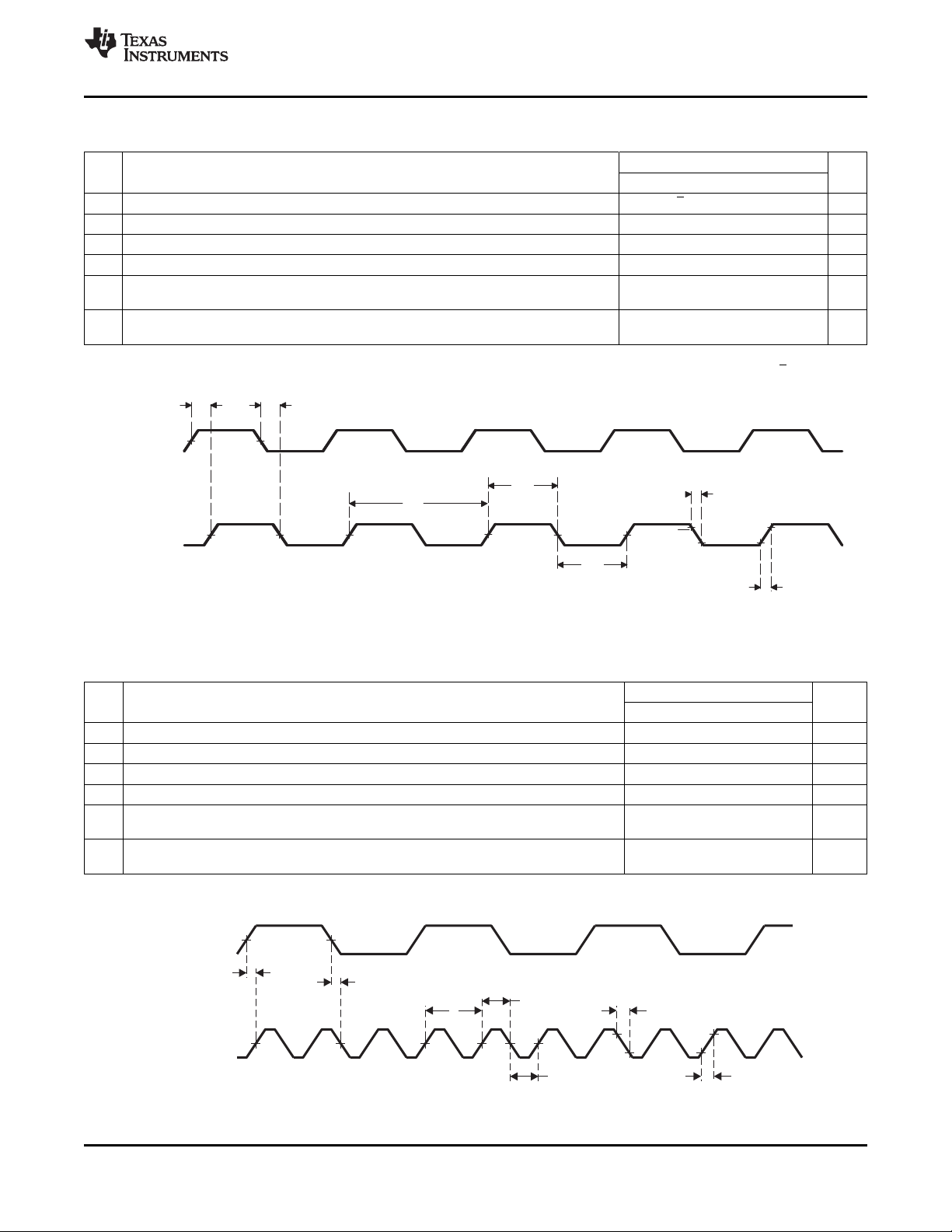
CLKOUT0/1
1
2
4
4
MXI1/CLKIN
5 6
3
MXI1/CLKIN
CLKOUT2
1
2
3
4
5
6
4
TMS320DM368
www.ti.com
Table 6-5. Switching Characteristics Over Recommended Operating Conditions for CLKOUT0/CLKOUT1
(2)
(see Figure 6-7)
NO. PARAMETER UNIT
1 t
C(CLKOUT0/CLKOUT1)
2 t
w(CLKOUT0H/CLKOUT1H)
3 t
w(CLKOUT0L/CLKOUT1L)
4 t
t(CLKOUT0/CLKOUT1)
5 t
d(MXI1H-CLKOUT0H/CLKOUT1H)
6 t
d(MXI1L-CLKOUT0L/CLKOUT1L)
Cycle time, CLKOUT0/CLKOUT1 27.7 ns
Pulse duration, CLKOUT0/CLKOUT1 high .45P .55P ns
Pulse duration, CLKOUT0/CLKOUT1 low .45P .55P ns
Transition time, CLKOUT0/CLKOUT1 3 ns
Delay time, MXI1/CLKIN1 high to CLKOUT0/CLKOUT1
high
Delay time, MXI1/CLKIN1I low to CLKOUT0/CLKOUT1
low
SPRS668B–APRIL 2010–REVISED NOVEMBER 2010
DEVICE
MIN TYP MAX
1 8 ns
1 8 ns
(1) The reference points for the rise and fall transitions are measured at VOLMAX and VOHMIN.
(2) P = 1/CLKOUT0/1 clock frequency in nanoseconds (ns). For example, when CLKOUT1 frequency is 24 MHz use P = 41.6 ns.
(1)
Figure 6-7. CLKOUT1 Timing
Table 6-6. Switching Characteristics Over Recommended Operating Conditions for CLKOUT2
Figure 6-8)
NO. PARAMETER UNIT
1 t
C(CLKOUT2)
2 t
w(CLKOUT2H)
3 t
w(CLKOUT2L)
4 t
t(CLKOUT2)
t
d(MXI1H-
5 Delay time, MXI1/CLKIN1 high to CLKOUT2 high 1 8 ns
CLKOUT2H)
t
d(MXI1L-
6 Delay time, MXI1/CLKIN1 low to CLKOUT2 low 1 8 ns
CLKOUT2L)
Cycle time, CLKOUT2 20 ns
Pulse duration, CLKOUT2 high .45P .55P ns
Pulse duration, CLKOUT2 low .45P .55P ns
Transition time, CLKOUT2 3 ns
MIN TYP MAX
(1) The reference points for the rise and fall transitions are measured at VOLMAX and VOHMIN.
(2) P = 1/CLKOUT2 clock frequency in nanoseconds (ns). For example, when CLKOUT2 frequency is 8 MHz use P = 125 ns.
DEVICE
(1) (2)
(see
Figure 6-8. CLKOUT2 Timing
Copyright © 2010, Texas Instruments Incorporated Peripheral Information and Electrical Specifications 83
Product Folder Link(s): TMS320DM368
Submit Documentation Feedback
Page 84

C1 C2
RTCXI
RTCXO V
SS_32k
Crystal
32.768kHz
C
L
C1C
2
(C1C2)
RTCXI
2
3
1
TMS320DM368
SPRS668B–APRIL 2010–REVISED NOVEMBER 2010
6.6.3 PRTCSS Oscillator
The device has an PRTCSS oscillator input/output pair (RTCXI/RTCXO) usable with external crystals or
ceramic resonators to provide clock inputs. The optimal frequency for the crystal is 32.768 kHz. The
electrical requirements and characteristics are described in this section. Figure 6-9 shows an example
circuit.
www.ti.com
Figure 6-9. RTCXI1 Oscillator
The load capacitors, C1 and C2, should be chosen such that the equation is satisfied (typical values are
C1 = C2 = 2 fF). CLin the equation below is the load specified by the crystal manufacturer. All discrete
components used to implement the oscillator circuit should be placed as close as possible to the
associated oscillator pins (RTCXI and RTCXO) and to the V
SS_32K
pin.
6.6.4 PRTCSS Electrical Data/Timing
Table 6-7. Timing Requirements for RTCXI
NO.
1 t
c(RTCXI)
2 t
w(RTCXIH)
3 t
w(RTCXIL)
(1) The reference points for the rise and fall transitions are measured at VILMAX and VIHMIN.
(2) C = MXI1/CLKIN1 cycle time in ns. For example, when MXI1/CLKIN1 frequency is 24 MHz use C = 41.6 ns.
Cycle time, RTCXI 30.5175 µs
Pulse duration, RTCXI high .45C .55C ns
Pulse duration, RTCXI low .45C .55C ns
(1) (2)
(see Figure 6-6)
DEVICE UNIT
MIN TYP MAX
(1)
84 Peripheral Information and Electrical Specifications Copyright © 2010, Texas Instruments Incorporated
Figure 6-10. RTCXI Timing
Submit Documentation Feedback
Product Folder Link(s): TMS320DM368
Page 85

TMS320DM368
www.ti.com
SPRS668B–APRIL 2010–REVISED NOVEMBER 2010
Table 6-8. Switching Characteristics Over Recommended Operating Conditions for RTC Oscillator
PARAMETER MIN TYP MAX UNIT
Start-up time (from power up until oscillating at stable frequency) 0.85 2 s
Oscillation frequency 32.768 kHz
Crystal ESR 70 kΩ
Frequency stability +/- 50 ppm
The load capacitors, C1 and C2, should be chosen such that the equation is satisfied (typical values are
C1 = C2 = 2 fF). CL in the equation is the load specified by the crystal manufacturer. All discrete
components used to implement the oscillator circuit should be placed as close as possible to the
associated oscillator pins (RTCXI and RTCXO) and to the V
SS_MX1
pin.
6.7 Power Management and Real Time Clock Subsystem (PRTCSS)
The Power Management and Real Time Clock Subsystem (PRTCSS) is used for calendar applications.
The PRTCSS has an independent power supply and can remain ON while the rest of the power supply is
turned OFF. The PRTCSS supports the following features:
• Real Time Clock (RTC)
– Simple day counter (Up to 89-years)
– To generate the Alarm event to check the RTC count
– 16-bit simple timer
– Watch-dog timer to generate the event for RTC-Sequencer
• General Purpose I/O with Anti-chattering
– 3-output pins (PWRCTRO[2:0])
– 7-In/Output pins (PWRCTRIO[6:0])
• Interrupt
– 2 RTCSS interrupts (ARMSS and Timer)
– 7 GPIO interrupts (PWRCTRIO[6:0]
6.7.1 PRTCSS Peripheral Register Description(s)
The following table lists the PRTCSS Interface registers (PRTCIF) and Table 6-10 lists the PRTCSS
registers which can only be accessed via the PRTCIF registers, their corresponding acronyms, and device
memory locations (offsets). For more details, see the TMS320DM36x PRTCSS User's Guide (literature
number SPRUFJ0).
Table 6-9. PRTC Interface (PRTCIF) Registers
Offset Acronym Register Description
0x0 PID PRTCIF peripheral ID register
0x4 PRTCIF_CTRL PRTCIF control register
0x8 PRTCIF_LDATA PRTCIF access lower data register
0xC PRTCIF_UDATA PRTCIF access upper data register
0x10 PRTCIF_INTEN PRTCIF interrupt enable register
0x14 PRTCIF_INTFLG PRTCIF interrupt flag register
Table 6-10. Power Management and Real Time Clock Subsystem (PRTCSS) Registers
Offset Acronym Register Description
0x0 GO_OUT Global output pin output data register
0x1 GIO_OUT Global input/output pin output data register
0x2 GIO_DIR Global input/output pin direction register
0x3 GIO_IN Global input/output pin input data register
Copyright © 2010, Texas Instruments Incorporated Peripheral Information and Electrical Specifications 85
Submit Documentation Feedback
Product Folder Link(s): TMS320DM368
Page 86

TMS320DM368
SPRS668B–APRIL 2010–REVISED NOVEMBER 2010
Table 6-10. Power Management and Real Time Clock Subsystem (PRTCSS) Registers (continued)
Offset Acronym Register Description
0x4 GIO_FUNC Global input/output pin function register
0x5 GIO_RISE_INT_EN GIO rise interrupt enable register
0x6 GIO_FALL_INT_EN GIO fall interrupt enable register
0x7 GIO_RISE_INT_FLG GIO rise interrupt flag register
0x8 GIO_FALL_INT_FLG GIO fall interrupt flag register
0x9 - 0xA Reserved Reserved
0xB INTC_EXTENA0 EXT interrupt enable 0 register
0xC INTC_EXTENA1 EXT interrupt enable 1 register
0xD INTC_FLG0 Event interrupt flag 0 register
0xE INTC_FLG1 Event interrupt flag 1 register
0x10 RTC_CTRL RTC control register
0x11 RTC_WDT Watchdog timer counter register
0x12 RTC_TMR0 Timer counter 0 register
0x13 RTC_TMR1 Timer counter 1 register
0x14 RTC_CCTRL Calender control register
0x15 RTC_SEC Seconds register
0x16 RTC_MIN Minutes register
0x17 RTC_HOUR Hours register
0x18 RTC_DAY0 Days[[7:0] register
0x19 RTC_DAY1 Days[14:8] register
0x1A RTC_AMIN Minutes Alarm register
0x1B RTC_AHOUR Hour Alarm register
0x1C RTC_ADAY0 Days[7:0] Alarm register
0x1D RTC_ADAY1 Days[14:8] Alarm register
0x20 CLKC_CNT Clock control register
www.ti.com
86 Peripheral Information and Electrical Specifications Copyright © 2010, Texas Instruments Incorporated
Submit Documentation Feedback
Product Folder Link(s): TMS320DM368
Page 87

TMS320DM368
www.ti.com
SPRS668B–APRIL 2010–REVISED NOVEMBER 2010
6.8 General-Purpose Input/Output (GPIO)
The GPIO peripheral provides general-purpose pins that can be configured as either inputs or outputs.
When configured as an output, a write to an internal register can control the state driven on the output pin.
When configured as an input, the state of the input is detectable by reading the state of an internal
register. In addition, the GPIO peripheral can produce CPU interrupts and EDMA events in different
interrupt/event generation modes. The GPIO peripheral provides generic connections to external devices.
The GPIO pins are grouped into banks of 16 pins per bank (i.e., bank 0 consists of GPIO [0:15]). There
are a total of 7 GPIO banks in the device, because the device has 104 GPIOs. For additional details on
GPIO pins voltage level and the associated power supply please see Table 6-11.
Table 6-11. GPIO Pin Voltage Level and Power Supply Reference
Voltage Level 1.8 V or 3.3 V 3.3 V 1.8 V
Power Supply Name V
Pin Name GIO[66:56] GIO[55:52] GIO[49:0]
DD_AEMIF1_18_33
GIO[78:68] GIO[67] GIO[103:93] GIO[92:79] GIO[110:104]
GIO[51:50]
The GPIO peripheral supports the following:
• Up to 104 GPIO pins, GPIO[103:0]
• Up to 7 GPIO pins dedicated to the PRTC Subsystem. These pins are labeled as PWRCTRIO[6:0].
Only PWRCTRIO[2:0] are connected to the GPIO module, labeled as GPIO[106:104]. For the PRTCSS
module the PWRCTRIO[6:0] pins support input and output functionality but for the GPIO module the
GPIO[106:104] pins support input functionality only. For more details please refer to Section 6.7.
• Interrupts:
– Up to 15 unique GPIO[15:0] interrupts from Bank 0.
– Up to 3 unique GPIO[106:104] interrupts from Bank 6, dedicated to the PRTC Subsystem. For
more details please refer to Section 6.7.
– Interrupts can be triggered by rising and/or falling edge, specified for each interrupt capable GPIO
signal
• DMA events:
– Up to 15 unique GPIO DMA events from Bank 0
• Set/clear functionality: Firmware writes 1 to corresponding bit position(s) to set or to clear GPIO
signal(s). This allows multiple firmware processes to toggle GPIO output signals without critical section
protection (disable interrupts, program GPIO, re-enable interrupts, to prevent context switching to
anther process during GPIO programming).
• Separate Input/Output registers
• Output register in addition to set/clear so that, if preferred by firmware, some GPIO output signals can
be toggled by direct write to the output register(s).
• Output register, when read, reflects output drive status. This, in addition to the input register reflecting
pin status, allows wired logic be implemented.
V
DD_AEMIF2_18_33
V
DD_ISIF18_33
V
DDS33
V
DD18_PRTCSS
For more detailed information on GPIOs, see the Documentation Support section for the General-Purpose
Input/Output (GPIO) Reference Guide.
Copyright © 2010, Texas Instruments Incorporated Peripheral Information and Electrical Specifications 87
Submit Documentation Feedback
Product Folder Link(s): TMS320DM368
Page 88

TMS320DM368
SPRS668B–APRIL 2010–REVISED NOVEMBER 2010
6.8.1 GPIO Peripheral Register Description(s)
Table 6-12 lists the GPIO registers, their corresponding acronyms, and device memory locations (offsets).
Table 6-12. General-Purpose Input/Output (GPIO) Registers
OFFSET ACRONYM REGISTER DESCRIPTION
0h PID Peripheral Identification Register
8h BINTEN GPIO Interrupt Per-Bank Enable Register
GPIO Banks 0 and 1
10h DIR01 GPIO Banks 0 and 1 Direction Register
14h OUT_DATA01 GPIO Banks 0 and 1 Output Data Register
18h SET_DATA01 GPIO Banks 0 and 1 Set Data Register
1Ch CLR_DATA01 GPIO Banks 0 and 1 Clear Data Register
20h IN_DATA01 GPIO Banks 0 and 1 Input Data Register
24h SET_RIS_TRIG GPIO Set Rising Edge Interrupt Register
28h CLR_RIS_TRIG GPIO Clear Rising Edge Interrupt Register
2Ch SET_FAL_TRIG GPIO Set Falling Edge Interrupt Register
30h CLR_FAL_TRIG GPIO Clear Falling Edge Interrupt Register
34h INTSTAT GPIO Interrupt Status Register
GPIO Banks 2 and 3
38h DIR23 GPIO Banks 2 and 3 Direction Register
3Ch OUT_DATA23 GPIO Banks 2 and 3 Output Data Register
40h SET_DATA23 GPIO Banks 2 and 3 Set Data Register
44h CLR_DATA23 GPIO Banks 2 and 3 Clear Data Register
48h IN_DATA23 GPIO Banks 2 and 3 Input Data Register
GPIO Bank 4 and 5
60h DIR45 GPIO Bank 4 and 5 Direction Register
64h OUT_DATA45 GPIO Bank 4 and 5 Output Data Register
68h SET_DATA45 GPIO Bank 4 and 5 Set Data Register
6Ch CLR_DATA45 GPIO Bank 4 and 5 Clear Data Register
70h IN_DATA45 GPIO Bank 4 and 5 Input Data Register
GPIO Bank 6
88h DIR6 GPIO Bank 6 Direction Register
8Ch OUT_DATA6 GPIO Bank 6 Output Data Register
90h SET_DATA6 GPIO Bank 6 Set Data Register
94h CLR_DATA6 GPIO Bank 6 Clear Data Register
98h IN_DATA6 GPIO Bank 6 Input Data Register
www.ti.com
6.8.2 GPIO Peripheral Input/Output Electrical Data/Timing
Table 6-13. Timing Requirements for GPIO Inputs (see Figure 6-11)
NO. UNIT
1 t
w(GPIH)
2 t
w(GPIL)
(1) P = PLLC1.SYSCLK4 period, where SYSCLK4 is an output clock of PLLC1. For more details, see Section 3.3, Device Clocking.
88 Peripheral Information and Electrical Specifications Copyright © 2010, Texas Instruments Incorporated
Pulse duration, GPIx high 12P
Pulse duration, GPIx low 12P
Submit Documentation Feedback
Product Folder Link(s): TMS320DM368
DEVICE
MIN MAX
(1)
(1)
ns
ns
Page 89

GPIx
GPOx
4
3
2
1
EXT_INTx
2
1
TMS320DM368
www.ti.com
SPRS668B–APRIL 2010–REVISED NOVEMBER 2010
Table 6-14. Switching Characteristics Over Recommended Operating Conditions for GPIO Outputs
(see Figure 6-11)
NO. PARAMETER UNIT
3 t
w(GPOH)
4 t
w(GPOL)
(1) P = PLLC1.SYSCLK4 period, where SYSCLK4 is an output clock of PLLC1. For more details, see Section 3.3, Device Clocking.
Pulse duration, GPOx high ns
Pulse duration, GPOx low ns
DEVICE
MIN MAX
(1)
36P
-
8
(1)
36P
-
8
Figure 6-11. GPIO Port Timing
6.8.3 GPIO Peripheral External Interrupts Electrical Data/Timing
Table 6-15. Timing Requirements for External Interrupts/EDMA Events
NO. UNIT
1 t
w(ILOW)
2 t
w(IHIGH)
(1) The pulse width given is sufficient to generate an interrupt or an EDMA event. However, if a user wants the device to recognize the
GPIO changes through software polling of the GPIO register, the GPIO duration must be extended to allow the device enough time to
access the GPIO register through the internal bus.
(2) P = PLLC1.SYSCLK4 period, where SYSCLK4 is an output clock of PLLC1. For more details, see Section 3.3, Device Clocking.
Width of the external interrupt pulse low 2P
Width of the external interrupt pulse high 2P
(1)
(see Figure 6-12)
DEVICE
MIN MAX
(2)
(2)
ns
ns
Figure 6-12. GPIO External Interrupt Timing
6.9 EDMA Controller
The EDMA controller handles all data transfers between memories and the device slave peripherals on
the device. These are summarized as follows:
• Transfer to/from on-chip memories
– ARM program/data RAM
– HDVICP Coprocessor memory
– MPEG/JPEG Coprocessor memory
• Transfer to/from external storage
– DDR2 / mDDR SDRAM
– Asynchronous EMIF
– OneNAND flash
– NAND flash, NOR flash
– Smart Media, SD, MMC, xD media storage
• Transfer to/from peripherals
– McBSP
– SPI
– I2C
Copyright © 2010, Texas Instruments Incorporated Peripheral Information and Electrical Specifications 89
Submit Documentation Feedback
Product Folder Link(s): TMS320DM368
Page 90

TMS320DM368
SPRS668B–APRIL 2010–REVISED NOVEMBER 2010
– PWM
– RTO
– GPIO
– Timer/WDT
– UART
– MMC/SD
The EDMA Controller consists of two major blocks: the Transfer Controller (TC) and the Channel
Controller (CC). The CC is a highly flexible Channel Controller that serves as the user interface and event
interface for the EDMA system. The CC supports 64-event channels and 8 QDMA channels. The CC
consists of a scalable Parameter RAM (PaRAM) that supports flexible ping-pong, circular buffering,
channel-chaining, auto-reloading, and memory protection.
The EDMA Channel Controller has the following features:
• Fully orthogonal transfer description
– Three transfer dimensions
– A-synchronized transfers: one dimension serviced per event
– AB- synchronized transfers: two dimensions serviced per event
– Independent indexes on source and destination
– Chaining feature allows 3-D transfer based on single event
• Flexible transfer definition
– Increment and constant addressing modes
– Linking mechanism allows automatic PaRAM set update
– Chaining allows multiple transfers to execute with one event
• Interrupt generation for:
– DMA completion
– Error conditions
• Debug visibility
– Queue watermarking/threshold
– Error and status recording to facilitate debug
• 64 DMA channels
– Event synchronization
– Manual synchronization (CPU(s) write to event set register)
– Chain synchronization (completion of one transfer chains to next)
• 8 QDMA channels
– QDMA channels are triggered automatically upon writing to a PaRAM set entry
– Support for programmable QDMA channel to PaRAM mapping
• 256 PaRAM sets
– Each PaRAM set can be used for a DMA channel, QDMA channel, or link set (remaining)
• Four transfer controllers/event queues. The system-level priority of these queues is user programmable
• 16 event entries per event queue
• External events (for example, McBSP TX Evt and RX Evt)
The EDMA Transfer Controller has the following features:
www.ti.com
• Four transfer controllers
• 64-bit wide read and write ports per channel
• Up to four in-flight transfer requests (TR)
• Programmable priority level
• Supports two dimensional transfers with independent indexes on source and destination (EDMA
Channel Controller manages the 3rd dimension)
90 Peripheral Information and Electrical Specifications Copyright © 2010, Texas Instruments Incorporated
Submit Documentation Feedback
Product Folder Link(s): TMS320DM368
Page 91

TMS320DM368
www.ti.com
• Support for increment and constant addressing modes
• Interrupt and error support
Parameter RAM: Each EDMA is specified by an eight word (32-byte) parameter table contained in
Parameter RAM (PaRAM) within the CC. The device provides 256 PaRAM entries, one for each of the 64
DMA channels and for 8 QDMA / Linked DMA entries.
DMA Channels: Can be triggered by: " External events (for example, McBSP TX Evt and RX Evt), "
Software writing a '1' to the given bit location, or channel, of the Event Set register, or, " Chaining to other
DMAs.
QDMA: The Quick DMA (QDMA) function is contained within the CC. The device implements 8 QDMA
channels. Each QDMA channel has a selectable PaRAM entry used to specify the transfer. A QDMA
transfer is submitted immediately upon writing of the "trigger" parameter (as opposed to the occurrence of
an event as with EDMA). The QDMA parameter RAM may be written by any Config bus master through
the Config Bus and by DMAs through the Config Bus bridge.
QDMA Channels: Triggered by a configuration bus write to a designated 'QDMA trigger word'. QDMAs
allow a minimum number of linear writes (optimized for GEM IDMA feature) to be issued to the CC to
force a series of transfers to take place.
6.9.1 EDMA Channel Synchronization Events
The EDMA supports up to 64 EDMA channels which service peripheral devices and external memory.
Table 6-16 lists the source of EDMA synchronization events associated with each of the programmable
EDMA channels. For the device, the association of an event to a channel is fixed; each of the EDMA
channels has one specific event associated with it. These specific events are captured in the EDMA event
registers (ER, ERH) even if the events are disabled by the EDMA event enable registers (EER, EERH).
For more detailed information on the EDMA module and how EDMA events are enabled, captured,
processed, linked, chained, and cleared, etc., see the Document Support section for the Enhanced Direct
Memory Access (EDMA) Controller Reference Guide.
SPRS668B–APRIL 2010–REVISED NOVEMBER 2010
Table 6-16. EDMA Channel Synchronization Events
EDMA
CHANNEL
0 TIMER3: TEVT6 Timer 3 Interrupt (TEVT6) Event
1 TIMER3 TEVT7 Timer 3 Interrupt (TEVT7) Event
2 McBSP Transmit Event or Voice Codec Transmit Event
3 McBSP Receive Event or Voice Codec Receive Event
4 VPSS: EVT1 VPSS Event 1
5 VPSS: EVT2 VPSS Event 2
6 VPSS: EVT3 VPSS Event 3
7 VPSS: EVT4 VPSS Event 4
8 TIMER2: TEVT4 Timer 2 interrupt (TEVT4) Event
9 TIMER2: TEVT5 Timer 2 interrupt (TEVT5) Event
10 SPI2: SPI2XEVT SPI2 Transmit Event
11 SPI2: SPI2REVT SPI2 Receive Event
(1) In addition to the events shown in this table, each of the 64 channels can also be synchronized with the transfer completion or
intermediate transfer completion events. For more detailed information on EDMA event-transfer chaining, see the Document Support
section for the Enhanced Direct Memory Access (EDMA) Controller Reference Guide.
(2) The total number of EDMA events exceeds 64, which is the maximum value of the EDMA module. Therefore, several events are
multiplexed and you must use the register EDMA_EVTMUX in the System Control Module to select the event source for multiplexed
events. Refer to the TMS320DM36x DMSoC ARM Subsystem Reference Guide (literature number SPRUFG5) for more information on
the System Control Module register EDMA_EVTMUX.
Copyright © 2010, Texas Instruments Incorporated Peripheral Information and Electrical Specifications 91
EVENT NAME EVENT DESCRIPTION
McBSP: XEVT or
VoiceCodec : VCREVT
McBSP :REVT or
VoiceCodec : VCREVT
Submit Documentation Feedback
Product Folder Link(s): TMS320DM368
(1) (2)
Page 92

TMS320DM368
SPRS668B–APRIL 2010–REVISED NOVEMBER 2010
Table 6-16. EDMA Channel Synchronization Events (continued)
EDMA
CHANNEL
12 HDVICP :
13 MJCP : SEQINT MPEG/JPEG Coprocessor SEQINT Event
14 SPI1: SPI1XEVT SPI1 Transmit Event
15 SPI1: SPI1REVT SPI1 Receive Event
16 SPI0: SPI0XEVT SP0I Transmit Event
17 SPI0: SPI0REVT SPI0 Receive Event
18 UART 0 Receive Event
19 UART 0 Transmit Event
20 UART1: URXEVT1 UART 1 Receive Event
21 UART1: UTXEVT1 UART 1 Transmit Event
22 TIMER4 : TEVT8 Timer 4 (TEVT8) Event
23 TIMER4 : TEVT9 Timer 4 (TEVT9) Event
24 RTOEVT Real Time Out Module Event
25 GPIO: GPINT9 GPIO 9 Event
26 MMC0RXEVT MMC/SD0 Receive Event
27 MMC0TXEVT MMC/SD0 Transmit Event
28 I2C : ICREVT I2C Receive Event
29 I2C : ICXEVT I2C Transmit Event
30 MMC1RXEVT MMC/SD1 Receive Event
31 MMC1TXEVT MMC/SD1 Transmit Event
32 GPIO :GPINT0 GPIO 0 Event
33 GPIO: GPINT1 GPIO 1 Event
34 GPIO :GPINT2 GPIO 2 Event
35 GPIO :GPINT3 GPIO 3 Event
36 GPIO :GPINT4 GPIO 4 Event
37 GPIO :GPINT5 GPIO 5 Event
38 GPIO :GPINT6 GPIO 6 Event
39 GPIO :GPINT7 GPIO 7 Event
40 GPIO 10 Event or EMAC EMACRXTHREESH
41 GPIO 11 Event or EMAC EMACRXPULSE
42 GPIO 12 Event or EMAC EMACTXPULSE
43 GPIO 13 Event or EMAC EMACMISCPULSE
44 GPIO : GPINT14 GPIO 14 Event
45 GPIO : GPINT15 GPIO 15 Event
46 ADC : ADINT Analog to Digital Converter Interrupt Event
47 GPIO : GPINT8 GPIO 8 Event
48 TIMER0 : TEVT0 Timer 0 (TEVT0) Event
49 TIMER0: TEVT1 Timer 1 (TEVT1) Event
50 TIMER1: TEVT2 Timer 2(TEVT2) Event
51 TIMER1: TEVT3 Timer 3(TEVT3) Event
52 PWM0 PWM 0 Event
EVENT NAME EVENT DESCRIPTION
MJCP : IMX0INT or
HDVICP_ARMINT
UART0: URXEVT0 or SPI3:
SPI3XEVT
UART0: UTXEVT0 or SPI3:
SPI3REVT
GPIO : GPINT10 or
EMACRXTHREESH
GPIO : GPINT11 or
EMACRXPULSE
GPIO : GPINT12 or
EMACTXPULSE
GPIO : GPINT13 or
EMACMISCPULSE
MPEG/JPEG Coprocessor IMX0INT Event or High Definition Video Image Coprocessor
HDVICP_ARMINT Event
www.ti.com
92 Peripheral Information and Electrical Specifications Copyright © 2010, Texas Instruments Incorporated
Submit Documentation Feedback
Product Folder Link(s): TMS320DM368
Page 93

TMS320DM368
www.ti.com
SPRS668B–APRIL 2010–REVISED NOVEMBER 2010
Table 6-16. EDMA Channel Synchronization Events (continued)
EDMA
CHANNEL
53 PWM1 or MJCP : IMX1INT PWM 1 Event or MJCP IMX1INT interrupt
54 PWM2 or MJCP : NSFINT PWM 2 Event or MJCP NSFINT interrupt
55
56
57
58
59
60
61
62
63
EVENT NAME EVENT DESCRIPTION
PWM3 or HDVICP(6) : MPEG/JPEG Coprocessor PWM 3 Event or High Definition Video Image Coprocessor
CP_UNDEF CP_UNDEF Event
MJCP : VLCDINT or MPEG/JPEG Coprocessor VLCDINT Event or High Definition Video Image Coprocessor
HDVICP(5) : CP_ECDCMP CP_ECDCMP Event
MJCP : BIMINT or MPEG/JPEG Coprocessor BIMINT Event or High Definition Video Image Coprocessor
HDVICP(8) : CP_ME CP_ME Event
MJCP : DCTINT or MPEG/JPEG Coprocessor DCTINT Event or High Definition Video Image Coprocessor
HDVICP(1) : CP_CALC CP_CALC Event
MJCP : QIQINT or MPEG/JPEG Coprocessor QIQINT Event or High Definition Video Image Coprocessor
HDVICP(7) : CP_IPE CP_IPE Event
MJCP : BPSINT or MPEG/JPEG Coprocessor BPSINT Event or High Definition Video Image Coprocessor
HDVICP(2) : CP_BS CP_BS Event
MJCP : VLCDERRINT or MPEG/JPEG Coprocessor VLCDERRINT Event or High Definition Video Image Coprocessor
HDVICP(0) : CP_LPF CP_LPF Event
MJCP : RCNTINT or MPEG/JPEG Coprocessor RCNTINT Event or High Definition Video Image Coprocessor
HDVICP(3) : CP_MC CP_MC Event
MJCP : COPCINT or MPEG/JPEG Coprocessor COPCINT Event or High Definition Video Image Coprocessor
HDVICP(4) : CP_ECDEND CP_ECDEND Event
6.9.2 EDMA Peripheral Register Description(s)
Table 6-17 lists the EDMA registers, their corresponding acronyms, and device memory locations
(offsets).
Table 6-17. EDMA Registers
Offset Acronym Register Description
00h PID Peripheral Identification Register
04h CCCFG EDMA3CC Configuration Register
Global Registers
0200h QCHMAP0 QDMA Channel 0 Mapping Register
0204h QCHMAP1 QDMA Channel 1 Mapping Register
0208h QCHMAP2 QDMA Channel 2 Mapping Register
020Ch QCHMAP3 QDMA Channel 3 Mapping Register
0210h QCHMAP4 QDMA Channel 4 Mapping Register
0214h QCHMAP5 QDMA Channel 5 Mapping Register
0218h QCHMAP6 QDMA Channel 6 Mapping Register
021Ch QCHMAP7 QDMA Channel 7 Mapping Register
0240h DMAQNUM0 DMA Queue Number Register 0
0244h DMAQNUM1 DMA Queue Number Register 1
0248h DMAQNUM2 DMA Queue Number Register 2
024Ch DMAQNUM3 DMA Queue Number Register 3
0250h DMAQNUM4 DMA Queue Number Register 4
0254h DMAQNUM5 DMA Queue Number Register 5
0258h DMAQNUM6 DMA Queue Number Register 6
025Ch DMAQNUM7 DMA Queue Number Register 7
0260h QDMAQNUM QDMA Queue Number Register
0284h QUEPRI Queue Priority Register
0300h EMR Event Missed Register
Copyright © 2010, Texas Instruments Incorporated Peripheral Information and Electrical Specifications 93
Submit Documentation Feedback
Product Folder Link(s): TMS320DM368
Page 94

TMS320DM368
SPRS668B–APRIL 2010–REVISED NOVEMBER 2010
Table 6-17. EDMA Registers (continued)
Offset Acronym Register Description
0304h EMRH Event Missed Register High
0308h EMCR Event Missed Clear Register
030Ch EMCRH Event Missed Clear Register High
0310h QEMR QDMA Event Missed Register
0314h QEMCR QDMA Event Missed Clear Register
0318h CCERR EDMA3CC Error Register
031Ch CCERRCLR EDMA3CC Error Clear Register
0320h EEVAL Error Evaluate Register
0340h DRAE0 DMA Region Access Enable Register for Region 0
0344h DRAEH0 DMA Region Access Enable Register High for Region 0
...
0350h DRAE2 DMA Region Access Enable Register for Region 2
0354h DRAEH2 DMA Region Access Enable Register High for Region 2
0360h DRAE4 DMA Region Access Enable Register for Region 4
0364h DRAEH4 DMA Region Access Enable Register High for Region 4
0368h DRAE5 DMA Region Access Enable Register for Region 5
036Ch DRAEH5 DMA Region Access Enable Register High for Region 5
0380h QRAE0 QDMA Region Access Enable Register for Region 0
0388h QRAE2 QDMA Region Access Enable Register for Region 2
0390h QRAE4
0394h QRAE5
0400h-047Ch Q0E0-Q1E15 Event Queue Entry Registers Q0E0-Q1E15
0600h QSTAT0 Queue 0 Status Register
0604h QSTAT1 Queue 1 Status Register
0608h QSTAT2 Queue 2 Status Register
060Ch QSTAT3 Queue 3 Status Register
0620h QWMTHRA Queue Watermark Threshold A Register
0640h CCSTAT EDMA3CC Status Register
Global Channel Registers
1000h ER Event Register
1004h ERH Event Register High
1008h ECR Event Clear Register
100Ch ECRH Event Clear Register High
1010h ESR Event Set Register
1014h ESRH Event Set Register High
1018h CER Chained Event Register
101Ch CERH Chained Event Register High
1020h EER Event Enable Register
1024h EERH Event Enable Register High
1028h EECR Event Enable Clear Register
102Ch EECRH Event Enable Clear Register High
1030h EESR Event Enable Set Register
1034h EESRH Event Enable Set Register High
1038h SER Secondary Event Register
103Ch SERH Secondary Event Register High
1040h SECR Secondary Event Clear Register
1044h SECRH Secondary Event Clear Register High
www.ti.com
94 Peripheral Information and Electrical Specifications Copyright © 2010, Texas Instruments Incorporated
Submit Documentation Feedback
Product Folder Link(s): TMS320DM368
Page 95

TMS320DM368
www.ti.com
Table 6-17. EDMA Registers (continued)
Offset Acronym Register Description
1050h IER Interrupt Enable Register
1054h IERH Interrupt Enable Register High
1058h IECR Interrupt Enable Clear Register
105Ch IECRH Interrupt Enable Clear Register High
1060h IESR Interrupt Enable Set Register
1064h IESRH Interrupt Enable Set Register High
1068h IPR Interrupt Pending Register
106Ch IPRH Interrupt Pending Register High
1070h ICR Interrupt Clear Register
1074h ICRH Interrupt Clear Register High
1078h IEVAL Interrupt Evaluate Register
1080h QER QDMA Event Register
1084h QEER QDMA Event Enable Register
1088h QEECR QDMA Event Enable Clear Register
108Ch QEESR QDMA Event Enable Set Register
1090h QSER QDMA Secondary Event Register
1094h QSECR QDMA Secondary Event Clear Register
Shadow Region 0 Channel Registers
2000h ER Event Register
2004h ERH Event Register High
2008h ECR Event Clear Register
200Ch ECRH Event Clear Register High
2010h ESR Event Set Register
2014h ESRH Event Set Register High
2018h CER Chained Event Register
201Ch CERH Chained Event Register High
2020h EER Event Enable Register
2024h EERH Event Enable Register High
2028h EECR Event Enable Clear Register
202Ch EECRH Event Enable Clear Register High
2030h EESR Event Enable Set Register
2034h EESRH Event Enable Set Register High
2038h SER Secondary Event Register
203Ch SERH Secondary Event Register High
2040h SECR Secondary Event Clear Register
2044h SECRH Secondary Event Clear Register High
2050h IER Interrupt Enable Register
2054h IERH Interrupt Enable Register High
2058h IECR Interrupt Enable Clear Register
205Ch IECRH Interrupt Enable Clear Register High
2060h IESR Interrupt Enable Set Register
2064h IESRH Interrupt Enable Set Register High
2068h IPR Interrupt Pending Register
206Ch IPRH Interrupt Pending Register High
2070h ICR Interrupt Clear Register
2074h ICRH Interrupt Clear Register High
2078h IEVAL Interrupt Evaluate Register
SPRS668B–APRIL 2010–REVISED NOVEMBER 2010
Copyright © 2010, Texas Instruments Incorporated Peripheral Information and Electrical Specifications 95
Submit Documentation Feedback
Product Folder Link(s): TMS320DM368
Page 96
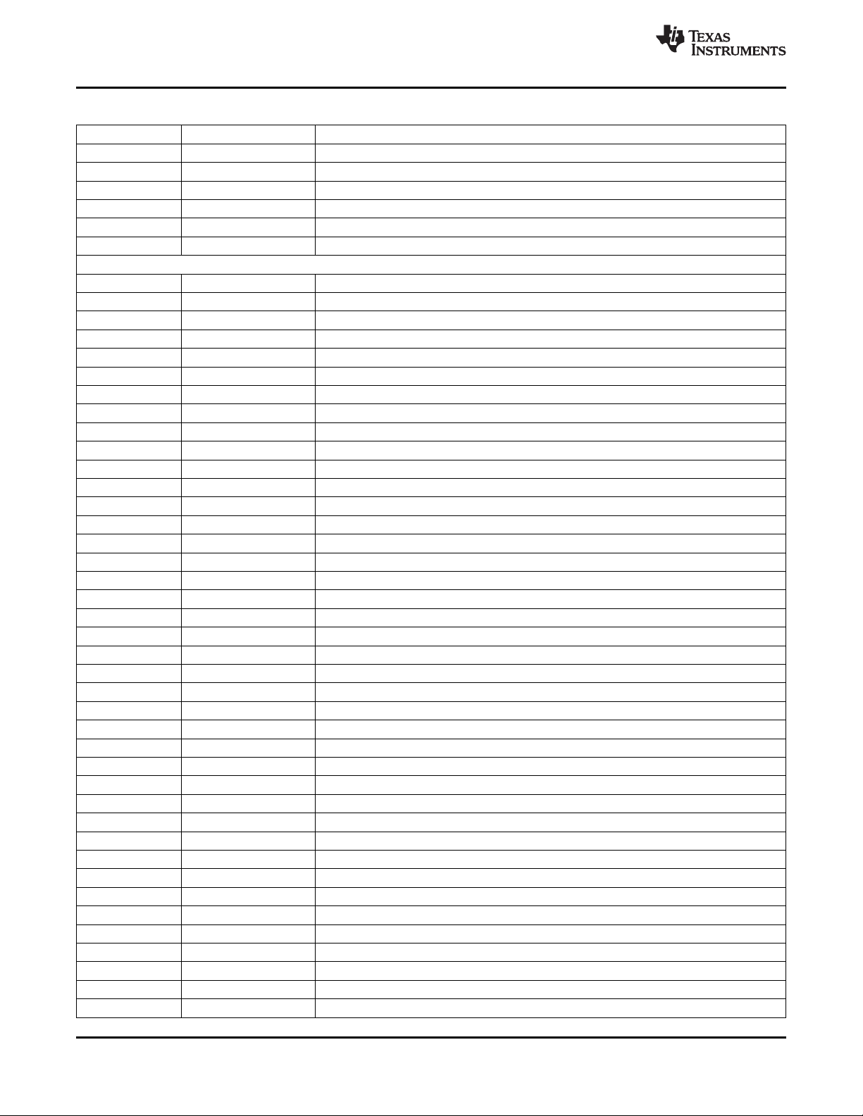
TMS320DM368
SPRS668B–APRIL 2010–REVISED NOVEMBER 2010
Table 6-17. EDMA Registers (continued)
Offset Acronym Register Description
2080h QER QDMA Event Register
2084h QEER QDMA Event Enable Register
2088h QEECR QDMA Event Enable Clear Register
208Ch QEESR QDMA Event Enable Set Register
2090h QSER QDMA Secondary Event Register
2094h QSECR QDMA Secondary Event Clear Register
Shadow Region 1 Channel Registers
2200h ER Event Register
2204h ERH Event Register High
2208h ECR Event Clear Register
220Ch ECRH Event Clear Register High
2210h ESR Event Set Register
2214h ESRH Event Set Register High
2218h CER Chained Event Register
221Ch CERH Chained Event Register High
2220h EER Event Enable Register
2224h EERH Event Enable Register High
2228h EECR Event Enable Clear Register
222Ch EECRH Event Enable Clear Register High
2230h EESR Event Enable Set Register
2234h EESRH Event Enable Set Register High
2238h SER Secondary Event Register
223Ch SERH Secondary Event Register High
2240h SECR Secondary Event Clear Register
2244h SECRH Secondary Event Clear Register High
2250h IER Interrupt Enable Register
2254h IERH Interrupt Enable Register High
2258h IECR Interrupt Enable Clear Register
225Ch IECRH Interrupt Enable Clear Register High
2260h IESR Interrupt Enable Set Register
2264h IESRH Interrupt Enable Set Register High
2268h IPR Interrupt Pending Register
226Ch IPRH Interrupt Pending Register High
2270h ICR Interrupt Clear Register
2274h ICRH Interrupt Clear Register High
2278h IEVAL Interrupt Evaluate Register
2280h QER QDMA Event Register
2284h QEER QDMA Event Enable Register
2288h QEECR QDMA Event Enable Clear Register
228Ch QEESR QDMA Event Enable Set Register
2290h QSER QDMA Secondary Event Register
2294h QSECR QDMA Secondary Event Clear Register
2400h-2494h — Shadow Region 2 Channel Registers
2600h-2694h — Shadow Region 3 Channel Registers
2800h-2894h Shadow Region 4 Channel Registers
2A00h-2A94h Shadow Region 5 Channel Registers
2C00h-2C94h Shadow Region 6 Channel Registers
www.ti.com
96 Peripheral Information and Electrical Specifications Copyright © 2010, Texas Instruments Incorporated
Submit Documentation Feedback
Product Folder Link(s): TMS320DM368
Page 97

TMS320DM368
www.ti.com
Table 6-17. EDMA Registers (continued)
Offset Acronym Register Description
2E00h-2E94h Shadow Region 7 Channel Registers
4000h-4FFFh — Parameter RAM (PaRAM)
Table 6-18 shows an abbreviation of the set of registers which make up the parameter set for each of 512
EDMA events. Each of the parameter register sets consist of 8 32-bit word entries. Table 6-19 shows the
parameter set entry registers with relative memory address locations within each of the parameter sets.
SPRS668B–APRIL 2010–REVISED NOVEMBER 2010
Copyright © 2010, Texas Instruments Incorporated Peripheral Information and Electrical Specifications 97
Submit Documentation Feedback
Product Folder Link(s): TMS320DM368
Page 98

TMS320DM368
SPRS668B–APRIL 2010–REVISED NOVEMBER 2010
Table 6-18. EDMA Parameter Set RAM
HEX ADDRESS RANGE DESCRIPTION
0x01C0 4000 - 0x01C0 401F Parameters Set 0 (8 32-bit words)
0x01C0 4020 - 0x01C0 403F Parameters Set 1 (8 32-bit words)
0x01C0 4040 - 0x01C0 405F Parameters Set 2 (8 32-bit words)
0x01C0 4060 - 0x01C0 407F Parameters Set 3 (8 32-bit words)
0x01C0 4080 - 0x01C0 409F Parameters Set 4 (8 32-bit words)
0x01C0 40A0 - 0x01C0 40BF Parameters Set 5 (8 32-bit words)
... ...
0x01C0 7FC0 - 0x01C0 7FDF Parameters Set 510 (8 32-bit words)
0x01C0 7FE0 - 0x01C0 7FFF Parameters Set 511 (8 32-bit words)
HEX OFFSET ADDRESS
WITHIN THE PARAMETER SET
0x0000 OPT Option
0x0004 SRC Source Address
0x0008 A_B_CNT A Count, B Count
0x000C DST Destination Address
0x0010 SRC_DST_BIDX Source B Index, Destination B Index
0x0014 LINK_BCNTRLD Link Address, B Count Reload
0x0018 SRC_DST_CIDX Source C Index, Destination C Index
0x001C CCNT C Count
www.ti.com
Table 6-19. Parameter Set Entries
ACRONYM PARAMETER ENTRY
98 Peripheral Information and Electrical Specifications Copyright © 2010, Texas Instruments Incorporated
Submit Documentation Feedback
Product Folder Link(s): TMS320DM368
Page 99

TMS320DM368
www.ti.com
6.10 External Memory Interface (EMIF)
The device supports several memory and external device interfaces, including:
• Asynchronous EMIF (AEMIF) for interfacing to SRAM.
– OneNAND flash memories
– NAND flash memories
– NOR flash memories
• DDR2/mDDR Memory Controller for interfacing to SDRAM.
6.10.1 Asynchronous EMIF (AEMIF)
The EMIF supports the following features:
• SRAM, NOR flash, etc. on up to 2 asynchronous chip selects addressable up to 16MB each
• Supports 8-bit or 16-bit data bus widths
• Programmable asynchronous cycle timings
• Supports extended wait mode
• Supports Select Strobe mode
6.10.1.1 NAND (NAND, SmartMedia, xD)
The NAND features of the EMIF are as follows:
• NAND flash on up to 2 asynchronous chip selects
• 8 and 16-bit data bus widths
• Programmable cycle timings
• Performs 1-bit and 4-bit ECC calculation
• NAND Mode also supports SmartMedia/SSFDC (Solid State Floppy Disk Controller) and xD memory
cards
SPRS668B–APRIL 2010–REVISED NOVEMBER 2010
6.10.1.2 OneNAND
The OneNAND features supported are as follows.
• NAND flash on up to 2 asynchronous chip selects
• Only 16-bit data bus widths
• Supports asynchronous writes and reads
• Supports synchronous reads with continuous linear burst mode (Does not support synchronous reads
with wrap burst modes)
• Programmable cycle timings for each chip select in asynchronous mode
6.10.1.3 EMIF Peripheral Register Descriptions
Table 6-20 lists the EDMA registers, their corresponding acronyms, and device memory locations
(offsets).
Table 6-20. External Memory Interface (EMIF) Registers
OFFSET ACRONYM REGISTER DESCRIPTION
04h AWCCR Asynchronous Wait Cycle Configuration
10h A1CR Asynchronous 1 Configuration Register (CE0
14h A2CR Asynchronous 2 Configuration Register (CE1
40h EIRR EMIF Interrupt Raw Register
44h EIMR EMIF Interrupt Mask Register
Register
space)
space)
Copyright © 2010, Texas Instruments Incorporated Peripheral Information and Electrical Specifications 99
Submit Documentation Feedback
Product Folder Link(s): TMS320DM368
Page 100

TMS320DM368
SPRS668B–APRIL 2010–REVISED NOVEMBER 2010
Table 6-20. External Memory Interface (EMIF) Registers (continued)
OFFSET ACRONYM REGISTER DESCRIPTION
48h EIMSR EMIF Interrupt Mask Set Register
4Ch EIMCR EMIF Interrupt Mask Clear Register
5Ch ONENANDCTL OneNAND Flash Control Register
60h NANDFCR NAND Flash Control Register
64h NANDFSR NAND Flash Status Register
70h NANDF1ECC NAND Flash 1-Bit ECC Register 1 (CE0
74h NANDF2ECC NAND Flash 1-Bit ECC Register 2 (CE1
BCh NAND4BITECCLOAD NANDFlash 4-Bit ECC Load Register
C0h NAND4BITECC1 NAND Flash 4-Bit ECC Register 1
C4h NAND4BITECC2 NAND Flash 4-Bit ECC Register 2
C8h NAND4BITECC3 NAND Flash 4-Bit ECC Register 3
CCh NAND3BITECC4 NAND Flash 4-Bit ECC Register 4
D0h NANDERRADD1 NAND Flash 4-Bit ECC Error Address
D4h NANDERRADD2 NAND Flash 4-Bit ECC Error Address
D8h NANDERRVAL1 NAND Flash 4-Bit ECC Error Value Register
DCh NANDERRVAL2 NAND Flash 4-Bit ECC Error Value Register
www.ti.com
Space)
Space)
Register 1
Register 2
1
2
100 Peripheral Information and Electrical Specifications Copyright © 2010, Texas Instruments Incorporated
Submit Documentation Feedback
Product Folder Link(s): TMS320DM368
 Loading...